1
Series AVME9630/9660 Industrial I/O Pack
VMEbus 3U/6U Non-Intelligent Carrier Boards
USER’S MANUAL
ACROMAG INCORPORATED
30765 South Wixom Road
P.O. BOX 437
Wixom, MI 48393-7037 U.S.A.
Tel: (248) 624-1541
Fax: (248) 624-9234
Copyright 1994, Acromag, Inc., Printed in the USA.
Data and specifications are subject to change without notice.
8500-482-G01B003
INDUSTRIAL I/O PACK SERIES AVME9630/9660
VMEbus 3U/6U CARRIER BOARDS
___________________________________________________________________________________________
The information contained in this manual is subject to change
without notice. Acromag, Inc. makes no warranty of any kind with
regard to this material, including, but not limited to, the implied
warranties of merchantability and fitness for a particular purpose.
Further, Acromag, Inc. assumes no responsibility for any errors that
may appear in this manual and makes no commitment to update, or
keep current, the information contained in this manual. No part of
this manual may be copied or reproduced in any form, without the
prior written consent of Acromag, Inc.
Table of Contents
1.0 GENERAL INFORMATION...............................................
KEY AVME9630/9660 FEATURES...................................
VMEbus INTERFACE FEATURES...................................
SIGNAL INTERFACE PRODUCTS..................................
INDUSTRIAL I/O PACK SOFTWARE LIBRARY..............
2.0 PREPARATION FOR USE................................................
UNPACKING AND INSPECTION.....................................
CARD CAGE CONSIDERATIONS...................................
BOARD CONFIGURATION..............................................
VMEbus INTERFACE CONFIGURATION.......................
Address Decode Jumper Configuration.........................
VMEbus Address Modifiers...........................................
Interrupt Configuration...................................................
CONNECTORS................................................................
Carrier Field I/O Connectors (IP modules A-D).............
IP Field I/O Connectors (IP modules A-D)....................
IP Logic Interface Connectors (IP modules A-D)..........
VMEbus Connections...................................................
POWER-UP TIMING AND LOADING.............................
DATA TRANSFER TIMING.............................................
FIELD GROUNDING CONSIDERATIONS.....................
3.0 PROGRAMMING INFORMATION..................................
MEMORY MAPS..............................................................
Identification PROM......................................................
Carrier Board Status Register.......................................
Interrupt Level Register.................................................
IP Error Register...........................................................
IP Memory Enable Register...........................................
IP Memory Base Address & Size Registers..................
IP Interrupt Enable Register..........................................
IP Interrupt Pending Register........................................
IP Interrupt Clear Register.............................................
GENERAL PROGRAMMING CONSIDERATIONS.........
Board Diagnostics.........................................................
GENERATING INTERRUPTS.........................................
Interrupt Configuration Example...................................
Sequence of Events for an Interrupt.............................
4.0 THEORY OF OPERATION..............................................
CARRIER BOARD OVERVIEW......................................
VMEbus Interface.........................................................
Carrier Board Registers................................................
IP Logic Interface..........................................................
Carrier Board Clock Circuitry........................................
IP Read and Write Cycle Timing..................................
VME Interrupter............................................................
Power Failure Monitor...................................................
Assess LEDs and Pulse Stretcher Circuitry.................
Power Supply Filters.....................................................
Page
2
2
3
3
3
4
4
4
4
4
4
4
5
5
5
5
5
5
6
6
6
6
6
8
8
8
9
9
9
10
10
10
10
10
11
11
11
11
11
11
12
12
12
12
12
13
13
13
-2-
5.0 SERVICE AND REPAIR....................................................
SERVICE AND REPAIR ASSISTANCE...........................
PRELIMINARY SERVICE PROCEDURE.........................
6.0 SPECIFICATIONS.............................................................
GENERAL SPECIFICATIONS..........................................
VMEbus COMPLIANCE....................................................
INDUSTRIAL I/O PACK COMPLIANCE...........................
13
13
13
13
13
14
14
APPENDIX.........................................................................
CABLE: MODEL 5025-550................................................
CABLE: MODEL 5025-551................................................
TERMINATION PANEL: MODEL 5025-552.....................
TRANSITION MODULE: MODEL TRANS-GP.................
15
15
15
15
15
DRAWINGS
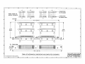
4501-450 AVME9630/9660 JUMPER & IP LOCATIONS
4501-434 MECHANICAL ASSEMBLY DRAWING..........
4501-451 AVME9630/9660 BLOCK DIAGRAM...............
4501-462 CABLE 5025-550 (NON-SHIELDED)..............
4501-463 CABLE 5025-551 (SHIELDED)........................
4501-464 TERMINATION PANEL 5025-552...................
4501-465 TRANSITION MODULE TRANS-GP...............
Page
16
16
17
17
18
18
19
IMPORTANT SAFETY CONSIDERATIONS
It is very important for the user to consider the possible adverse
effects of power, wiring, component, sensor, or software failures in
designing any type of control or monitoring system. This is
especially important where economic property loss or human life is
involved. It is important that the user employ satisfactory overall
system design. It is agreed between the Buyer and Acromag, that
this is the Buyer's responsibility.
1.0 GENERAL INFORMATION
The AVME9630/9660 Series of VMEbus cards are carriers for
the Industrial I/O Pack (IP) mezzanine board field I/O modules. The
carrier boards facilitate a modular approach to system assembly,
since each carrier can be populated with any combination of analog
input/output and digital input/output IP modules. Thus, the user can
create a board which is customized to the application which saves
money and space - a single carrier board populated with IP modules
may replace several dedicated function VMEbus boards. The
AVME9630/9660 non-intelligent carrier boards provide impressive
functionality at low cost.
Models are available in two standard VMEbus sizes, 3U and 6U,
with support for up to two and four IP modules, respectively.
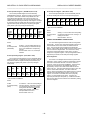
MODEL
AVME9630
AVME9660
AVME9630E
AVME9660E
VMEbus
Board Size
3U
6U
3U
6U
Supported IP
Slots
2 (A & B)
4 (A,B,C,D)
2 (A & B)
4 (A,B,C,D)
Operating
Temperature Range
0 to +70 °C
0 to +70 °C
-40 to +85°C
-40 to +85°C
INDUSTRIAL I/O PACK SERIES AVME9630/9660
VMEbus 3U/6U CARRIER BOARDS
___________________________________________________________________________________________
•
KEY AVME9630/9660 FEATURES
•
•
•
•
•
•
•
•
•
•
Interface for Two or Four IP Modules - Provides an
electrical and mechanical interface for up to four industry
standard IP modules. IP Modules are available from Acromag
and other vendors in a wide variety of Input/Output
configurations to meet the needs of varied applications.
Provides Full IP Data Access - Supports accesses to IP
input/output, memory, and ID PROM data spaces.
Full IP Register Access - Makes maximum use of logically
organized programmable registers on the carrier boards to
provide for easy configuration and control of IP modules. The
only hardware jumper settings required on the carrier boards
set the base address of the card in the VMEbus short I/O
space.
LED Displays Simplify Debugging - Front panel LED's are
dedicated to each IP module to give a visual indication of
successful IP accesses.
Front Panel Connectors Access I/O - Front panel access to
field I/O signals is provided via industry standard 50-pin
headers. A separate header is provided for each IP module.
All headers can be connected to flat ribbon cable from the front
panel without interference from boards in adjacent slots.
Ejector latches on the headers provide for excellent connection
integrity and easy cable removal.
Optional Screw Termination Panel - Model supports field
connection via screw terminals using the optional DIN rail
mount termination panels.
Memory Space Access Support - IP memory space
accesses are supported and software configurable from
1Mbyte to 8Mbytes in the VMEbus standard address space.
Supports Two Interrupt Channels per IP - Up to two
interrupt requests are supported for each IP. The VMEbus
interrupt level is software programmable. Additional registers
are associated with each interrupt request for control and
status monitoring.
Supervisory Circuit for Reset Generation - A
microprocessor supervisor circuit provides power-on, poweroff, and low power detection reset signals to the IP modules per
the IP specification.
Individually Filtered Power - Filtered +5V, +12V, and -12V
DC power is provided to the IP modules via passive filters
present on each supply line serving each IP. This provides
optimum filtering and isolation between the IP modules and the
carrier board and allows analog signals to be accurately
measured or reproduced on IP modules without signal
degradation from the carrier board logic signals.
Interrupt Support - I(1-7) interrupter D16/D08 (O). Up to two
interrupt requests are supported for each IP module. The
VMEbus interrupt level is software programmable. Carrier
board software programmable registers are utilized as interrupt
request control and status monitors. Interrupt release
mechanism is Release On Register Access (RORA) type.
SIGNAL INTERFACE PRODUCTS
(See Appendix for more information on compatible products)
This IP carrier board will mate directly to all industry standard IP
modules. Acromag provides the following interface products (all
connections to field signals are made through the carrier board
which passes them to the individual IP modules):
Cables:
Model 5025-551-X (Shielded Cable) or Model 5025-550-X (NonShielded Cable): A Flat 50-pin cable with female connectors at
both ends for connecting AVME9630/9660, or other compatible
carrier boards, to Model 5025-552 termination panels. The
unshielded cable is recommended for digital I/O, while the
shielded cable is recommended for optimum performance with
precision analog I/O applications.
Termination Panel:
Model 5025-552: DIN-rail mountable panel provides 50 screw
terminals for universal field I/O termination. Connects to
Acromag AVME9630/9660, or other compatible carrier boards,
via flat 50-pin ribbon cable (Model 5025-550-X or 5025-551-X).
Transition Module:
Model TRANS-GP: This module repeats field I/O connections
of IP modules A through D for rear exit from the card cage. It is
available for use in card cages which provide rear exit for I/O
connections via transition modules (transition modules can only
be used in card cages specifically designed for them). It is a
double-height (6U), single-slot module with front panel hardware
adhering to the VMEbus mechanical dimensions, except for
shorter printed circuit board depth. Connects to Acromag
Termination Panel 5025-552 from the rear of the card cage, and
to AVME9630/ 9660 boards within the card cage, via flat 50-pin
ribbon cable within the card cage (cable Model 5025-550-X or
5025-551-X).
VMEbus INTERFACE FEATURES
INDUSTRIAL I/O PACK SOFTWARE LIBRARY
•
Acromag provides an Industrial I/O Pack Software Library
diskette (Model IPSW-LIB-M03-1.44MB, MSDOS format) to simplify
communication with Acromag IP modules. All functions are written
in the “C” programming language and can be linked to your
application. Refer to the “README.TXT” file in the root directory on
the diskette for more details and the “96X0.TXT” files of the
“AVME9660/9630” subdirectories that correspond to your carrier
model.
•
•
•
Slave ModuleCarrier Register Short I/O Access A16, D16/D08(O)
IP Module ID Space
A16, D16/D08(O)
IP Module I/O Space
A16, D16/D08(EO)
IP Module Memory Space
A24, D16/D08(EO)
Supports Short I/O Address Modifiers - Supports short I/O
(A16) address modifiers 29H, 2DH (H = Hex). Short I/O space
is used for all carrier registers and IP module I/O and ID
spaces. The carrier board base address is set by hardware
jumpers and decoded on 1K byte boundaries.
Supports Standard I/O Address Modifiers - Supports
standard (A24) address modifiers 39H, 3DH (H = Hex).
Standard address space is used when an IP supports memory
space. The carrier board is configured using programmable
registers to set the IP starting address and size (1Mbyte to
8Mbytes).
Supports Read-Modify-Write Cycles - Carrier board
supports VMEbus read-modify-write cycles.
-3-
INDUSTRIAL I/O PACK SERIES AVME9630/9660
VMEbus 3U/6U CARRIER BOARDS
___________________________________________________________________________________________
2.0 PREPARATION FOR USE
VMEbus INTERFACE CONFIGURATION
UNPACKING AND INSPECTION
The carrier board is shipped from the factory configured as
follows:
Upon receipt of this product, inspect the shipping carton for
evidence of mishandling during transit. If the shipping carton is
badly damaged or water stained, request that the carrier's agent be
present when the carton is opened. If the carrier's agent is absent
when the carton is opened and the contents of the carton are
damaged, keep the carton and packing material for the agent's
inspection.
•
•
•
For repairs to a product damaged in shipment, refer to the
Acromag Service Policy to obtain return instructions. It is
suggested that salvageable shipping cartons and packing material
be saved for future use in the event the product must be shipped.
Carrier board with VMEbus Short I/O Base Address of 0000H.
Board will respond to both Address Modifiers 29H and 2DH.
Registers on the carrier board plus the I/O and ID spaces on
any installed IP modules will be accessible.
Programmable software registers default to IP memory space
(VMEbus standard address space) accesses disabled.
Programmable software registers default to IP interrupt
requests-disabled and VMEbus interrupt level-none.
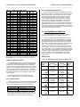
Address Decode Jumper Configuration
The carrier board interfaces with the VMEbus as a 1K byte
block of address locations in the VMEbus short I/O address space
(refer to Section 3 for memory map details). J1 decodes the six
most significant address lines A10 through A15 to provide segments
of 1K address space. The configuration of the jumpers for different
base address locations is shown in Table 2.1. "IN" means that the
pins are shorted together with a shorting clip. "OUT" indicates that
the clip has been removed.
This board is physically protected
with packing material and electrically
protected with an anti static bag
during shipment. It is recommended
that the board be visually inspected
for evidence of mishandling prior to
applying power.
Table 2.1:
Base
Addr*
(Hex)
0000
0400
0800
0C00
1000
.
.
.
EC00
F000
F400
F800
FC00
The board utilizes static sensitive
components and should only be
handled at a static-safe workstation.
CARD CAGE CONSIDERATIONS
Refer to the specifications for loading and power requirements.
Be sure that the system power supplies are able to accommodate
the power requirements of the carrier board, plus the installed IP
modules, within the voltage tolerances specified.
IMPORTANT: Adequate air circulation must be provided to prevent
a temperature rise above the maximum operating temperature.
Address Decode Jumper Selections (J1 Pins)
A15
(11&12)
OUT
OUT
OUT
OUT
OUT
.
.
.
IN
IN
IN
IN
IN
A14
(9&10)
OUT
OUT
OUT
OUT
OUT
.
.
.
IN
IN
IN
IN
IN
A13
(7&8)
OUT
OUT
OUT
OUT
OUT
.
.
.
IN
IN
IN
IN
IN
A12
(5&6)
OUT
OUT
OUT
OUT
IN
.
.
.
OUT
IN
IN
IN
IN
A11
(3&4)
OUT
OUT
IN
IN
OUT
.
.
.
IN
OUT
OUT
IN
IN
A10
(1&2)
OUT
IN
OUT
IN
OUT
.
.
.
IN
OUT
IN
OUT
IN
* Consult your host CPU manual for detailed information about
addressing the VMEbus short I/O (A16, 16-bit) space. In many
cases, CPU's utilizing 24-bit addressing will start the 16-bit
address at FF0000 (Hex), and 32-bit CPU's at FFFF0000 (Hex).
The dense packing of the IP modules to the carrier board
restricts air flow within the card cage and is cause for concern.
Adequate air circulation must be provided to prevent a temperature
rise above the maximum operating temperature and to prolong the
life of the electronics. If the installation is in an industrial
environment and the board is exposed to environmental air, careful
consideration should be given to air-filtering.
VMEbus Address Modifiers
No hardware jumper configuration is needed. The carrier board
will respond to both address modifiers 29H and 2DH in the VMEbus
short I/O space. This means that both short supervisory and short
non-privileged accesses are supported.
BOARD CONFIGURATION
The carrier board may be configured for different applications.
All possible configuration settings will be discussed in the following
Sections. The jumper locations and IP module positions are shown
in Drawing 4501-450. Power should be removed from the board
when installing IP modules, cables, termination panels, and field
wiring. Refer to Mechanical Assembly Drawing 4501-434 and your
IP module documentation for specific configuration and assembly
instructions.
The carrier board will respond to both address modifiers 39H
and 3DH in the VMEbus standard address space, when standard
address space accesses to IP memory are enabled via
programmable registers on the carrier board (refer to Section 3 for
programming details).
-4-
INDUSTRIAL I/O PACK SERIES AVME9630/9660
VMEbus 3U/6U CARRIER BOARDS
___________________________________________________________________________________________
Pin assignments for these connectors are defined by the IP
module specification and are shown in Table 2.2:
Interrupt Configuration
No hardware jumper configuration is required. All interrupt
enabling, status, and VMEbus interrupt level selections are
configured via programmable registers on the carrier board (see
Section 3 for programming details). The carrier board passes
interrupt requests from the IP modules to the VMEbus--It does not
originate interrupt requests. Refer to the IP modules for their
specific configuration requirements.
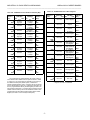
Table 2.2: Standard IP Logic Interface Connections (P11-P14)
Pin Description
Number
Pin Description
Number
GND
1
GND
26
CLK
2
+5V
27
Reset*
3
R/W*
28
D00
4
IDSEL*
29
D01
5
30
DMAReq0*
D02
6
MEMSEL*
31
D03
7
32
DMAReq1*
D04
8
IntSel*
33
D05
9
34
DMAck0*
D06
10
IOSEL*
35
D07
11
36
RESERVED
D08
12
A1
37
D09
13
38
DMAEnd*
D10
14
A2
39
D11
15
ERROR*
40
D12
16
A3
41
D13
17
INTReq0*
42
D14
18
A4
43
D15
19
INTReq1*
44
BS0*
20
A5
45
BS1*
21
46
STROBE*
-12V
22
A6
47
+12V
23
ACK*
48
+5V
24
49
RESERVED
GND
25
GND
50
CONNECTORS
Carrier Field I/O Connectors (IP modules A through D)
Field I/O connections are made via front panel connectors A, B,
C, and D for IP modules in positions A through D, respectively (C &
D not used on AVME9630). IP module assignment is marked on the
front panel for easy identification (see jumper & IP location drawing
4501-450 for physical locations of the IP modules). Flat cable
assemblies and Acromag termination panels (or user defined
terminations) can be quickly mated to the front panel connectors.
Pin assignments are defined by the IP module employed since the
pins from the IP module field side correspond identically to the pin
numbers of the front panel connectors.
Connectors A through D are 50-pin header (male) connectors
(3M 3433-D303). Connectors are high-density, stacked ("Condo")
type with A & B and C & D residing on the same part. These
connectors include long ejector latches and 30 microns of gold in the
mating area for excellent connection integrity (per MIL-G-45204,
Type II, Grade C).
IP Field I/O Connectors (IP modules A through D)
The field side connectors of IP modules A through D mate to
connectors P7-P10, respectively, on the carrier board (P9 & P10 are
not used on Model AVME9630). IP location is silk-screened on the
board for easy identification. Field and logic side connectors are
keyed to avoid incorrect assembly.
Asterisk (*) is used to indicate an active-low signal.
BOLD ITALIC Logic Lines are NOT USED by the carrier board.
P7-P10 are 50-pin plug header (male) connectors. These AMP
173280-3 connectors mate to AMP 173279-3 connectors (or similar)
on the IP modules. This provides excellent connection integrity and
utilizes gold plating in the mating area. Threaded metric M2 screws
and spacers (supplied with Acromag IP modules) provide additional
stability for harsh environments (see Drawing 4501-434 for
assembly details).
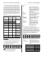
Table 2.3 indicates the pin assignments for the VMEbus signals
at the P1 connector. The P1 connector is the upper rear connector
on the AVME9630/9660 board, as viewed from the front. The
connector consists of 32 rows of three pins labeled A, B, and C. Pin
A1 is located at the upper left hand corner of the connector if the
board is viewed from the front. VMEbus connector P2 is not used.
VMEbus Connections
Refer to the VMEbus specification for additional information on
the VMEbus signals.
Pin assignments for these connectors are made by the specific
IP model used and correspond identically to the pin numbers of the
front panel connectors.
IP Logic Interface Connectors (IP modules A through D)
The logic interface sides of IP modules A through D mate to
connectors P11-P14 (P13 & P14 are not used on Model
AVME9630), respectively, on the carrier board. IP location is silkscreened on the board for easy identification. Field and logic side
connectors are keyed to avoid incorrect assembly.
P11-P14 are 50-pin male plug header connectors. These AMP
173280-3 connectors mate to AMP 173279-3 connectors (or similar)
on the IP modules. This provides excellent connection integrity and
utilizes gold plating in the mating area. Threaded metric M2 screws
and spacers (supplied with Acromag IP modules) provide additional
stability for harsh environments (see Drawing 4501-434 for
assembly details).
-5-
INDUSTRIAL I/O PACK SERIES AVME9630/9660
VMEbus 3U/6U CARRIER BOARDS
___________________________________________________________________________________________
TABLE 2.3: VMEbus P1 CONNECTIONS
FIELD GROUNDING CONSIDERATIONS
Pin Description Pin Description Pin Description
1A
D00
1B
1C
D08
BBSY*
2A
D01
2B
2C
D09
BCLR*
3A
D02
3B
3C
D10
ACFAIL*
4A
D03
4B
BG0IN*
4C
D11
5A
D04
5B
BG0OUT*
5C
D12
6A
D05
6B
BG1IN*
6C
D13
7A
D06
7B
BG1OUT*
7C
D14
8A
D07
8B
BG2IN*
8C
D15
9A
GND
9B
BG2OUT*
9C
GND
10A
SYSCLK
10B
BG3IN*
10C
SYSFAIL*
11A
GND
11B
BG3OUT*
11C
BERR*
12A
DS1*
12B
12C SYSRESET*
BR0*
13A
DS0*
13B
13C
LWORD*
BR1*
14A
WRITE*
14B
14C
AM5
BR2*
15A
GND
15B
15C
A23
BR3*
16A
DTACK*
16B
AM0
16C
A22
17A
GND
17B
AM1
17C
A21
18A
AS*
18B
AM2
18C
A20
19A
GND
19B
AM3
19C
A19
20A
IACK*
20B
GND
20C
A18
21A
IACKIN*
21B
21C
A17
SERCLK
22A
IACKOUT* 22B
22C
A16
SERDAT*
23A
AM4
23B
GND
23C
A15
24A
A07
24B
IRQ7*
24C
A14
25A
A06
25B
IRQ6*
25C
A13
26A
A05
26B
IRQ5*
26C
A12
27A
A04
27B
IRQ4*
27C
A11
28A
A03
28B
IRQ3*
28C
A10
29A
A02
29B
IRQ2*
29C
A09
30A
A01
30B
IRQ1*
30C
A08
31A
-12V
31B +5V STDBY 31C
+12V
32A
+5V
32B
+5V
32C
+5V
Asterisk (*) is used to indicate an active-low signal.
BOLD ITALIC Logic Lines are NOT USED by the carrier board.
This Section provides the specific information necessary to
operate the AVME9630/9660 non-intelligent carrier boards.
POWER-UP TIMING AND LOADING
Table 3.1A: AVME9630 3U Carrier Bd Short I/O Memory Map
The AVME9630/9660 boards use a Field Programmable GateArray (FPGA) to handle the bus interface and control logic timing.
Upon power-up, the FPGA automatically clocks in configuration
vectors from a local PROM to initialize the logic circuitry for normal
operation. This time is measured as the first 145mS (typical) after
the +5 Volt supply rises to +2.5 Volts at power-up. The VMEbus
specification requires that the bus master drive the system reset for
the first 200mS after power-up, thus inhibiting any data transfers
from taking place.
Base
Address +
EVEN Byte
(Hex)
D15
D08
IP A
0000
I/O Space
↓
High Byte
007E
0080
Not Used
↓
00BE
00C0
Not Used
↓
00FE
IP B
0100
I/O Space
↓
High Byte
017E
0180
Not Used
↓
01BE
01C0
Not Used
↓
01FE
0200
Not Used
↓
03FE
Carrier boards are designed with passive filters on each supply
line to each IP module. This provides maximum filtering and signal
isolation between the IP modules and the carrier board. However,
the boards are considered non-isolated, since there is electrical
continuity between the VMEbus and the IP grounds. Therefore,
unless isolation is provided on the IP module itself, the field I/O
connections are not isolated from the VMEbus. Care should be
taken in designing installations without isolation to avoid ground
loops and noise pickup. This is particularly important for analog I/O
applications when a high level of accuracy/resolution is needed (12bits or more). Contact your Acromag representative for information
on our many isolated signal conditioning products that could be used
to interface to the IP input/output modules.
3.0 PROGRAMMING INFORMATION
The board is addressable on 1K byte boundaries in the Short
I/O (A16) Address Space. This Acromag VMEbus non-intelligent
slave (carrier board) has a Board Status register, but no ID PROM.
ID PROM’s are provided per the Industrial I/O Pack logic interface
specification on the mezzanine (IP) boards which are installed on the
carrier. The 1K byte of memory consumed by the board is
composed of blocks of memory for the I/O and ID spaces of up to
four IP modules. The rest of the 1K byte address space is unused,
or contains registers or memory specific to the function of the carrier
board. The memory map for AVME9630 and AVME9660 are shown
in Tables 3.1A and 3.1B respectively. Note that the memory maps
for the two models are identical for IP modules A and B and the
control register locations. The AVME9630 does not contain IP
modules C or D.
MEMORY MAPS
IP control registers are also reset following a power-up
sequence, disabling interrupts, etc. (see Section 3 for details).
DATA TRANSFER TIMING
VMEbus data transfer time is measured from the falling edge of
DSx* to the falling edge of DTACK* during a normal data transfer
cycle. Typical transfer times are given in the following table.
Register
All Carrier Registers
IP Registers
Data Transfer Time
500 nS, Typical.
750 nS, Typical, If No Wait States*
* See IP module specifications for information on wait states. IP
module register access time will increase by the number of wait
states multiplied by 125nS (the period of the 8 MHz clock).
-6-
ODD Byte
D07
D00
IP A
I/O Space
Low Byte
IP A
ID Space
Low Byte
Carrier Board
Registers
(See Table 3.1C)
IP B
I/O Space
Low Byte
IP B
ID Space
Low Byte
Not Used
Not Used
Base
Address +
(Hex)
0001
↓
007F
0081
↓
00BF
00C1
↓
00FF
0101
↓
017F
0181
↓
01BF
01C1
↓
01FF
0201
↓
03FF
INDUSTRIAL I/O PACK SERIES AVME9630/9660
VMEbus 3U/6U CARRIER BOARDS
___________________________________________________________________________________________
Table 3.1C: AVME9630/9660 Carrier Board Registers
Table 3.1B: AVME9660 6U Carrier Bd Short I/O Memory Map
Base
Address +
EVEN Byte
(Hex)
D15
D08
IP A
0000
I/O Space
↓
High Byte
007E
0080
Not Used
↓
00BE
00C0
Not Used
↓
00FE
IP B
0100
I/O Space
↓
High Byte
017E
0180
Not Used
↓
01BE
01C0
Not Used
↓
01FE
IP C
0200
I/O Space
↓
High Byte
027E
0280
Not Used
↓
02BE
02C0
Not Used
↓
02FE
IP D
0300
I/O Space
↓
High Byte
037E
0380
Not Used
↓
03BE
03C0
Not Used
↓
03FE
ODD Byte
D07
D00
IP A
I/O Space
Low Byte
IP A
ID Space
Low Byte
Carrier Board
Registers
(See Table 3.1C)
IP B
I/O Space
Low Byte
IP B
ID Space
Low Byte
Not Used
IP C
I/O Space
Low Byte
IP C
ID Space
Low Byte
Not Used
IP D
I/O Space
Low Byte
IP D
ID Space
Low Byte
Not Used
Base
Address +
EVEN Byte
(Hex)
D15
D08
00C0
Not Used
Base
Address +
(Hex)
0001
↓
007F
0081
↓
00BF
00C1
↓
00FF
0101
↓
017F
0181
↓
01BF
01C1
↓
01FF
0201
↓
027F
0281
↓
02BF
02C1
↓
02FF
0301
↓
037F
0381
↓
03BF
03C1
↓
03FF
ODD Byte
D07
D00
Carrier Board
Status Register
Base
Address +
(Hex)
00C1
Not Used
Interrupt Level
Register
Not Used
IP Error
Register
Not Used
IP Memory
Enable Register
00C2
00C3
00C4
00C5
00C6
00C8
↓
00CE
00D0
Not Used
Not Used
00D2
Not Used
00D4
Not Used
00D6
Not Used
00D8
↓
00DE
00E0
Not Used
IP_A Memory
Base Address &
Size Register
IP_B Memory
Base Address &
Size Register
IP_C Memory
Base Address &
Size Register*
IP_D Memory
Base Address &
Size Register*
Not Used
Not Used
Not Used
IP Interrupt
Enable Register
Not Used
IP Interrupt
Pending Register
Not Used
IP Interrupt
Clear Register
00C7
00C9
↓
00CF
00D1
00D3
00D5
00D7
00D9
↓
00DF
00E1
00E2
00E3
00E4
00E6
↓
00FE
The Input/Output (IO) and Identification (ID) spaces of each IP
are accessible via the VMEbus Short I/O space as shown in Tables
3.1A and 3.1B. The carrier board may optionally occupy memory in
the VMEbus standard (A24) address space, if needed for IP
modules containing Memory space. IP memory will only be mapped
into the standard memory space if it is enabled for a particular IP per
the user programmable IP Memory Enable Register (see Table 3.1C
and subsequent description). The starting memory address for each
enabled IP and the memory size for each enabled IP module is userprogrammable via its associated IP Memory Base Address & Size
Register (see Table 3.1C and subsequent description).
Not Used
Not Used
* Registers not used on AVME9630.
-7-
00E5
00E7
↓
00FF
INDUSTRIAL I/O PACK SERIES AVME9630/9660
VMEbus 3U/6U CARRIER BOARDS
___________________________________________________________________________________________
Identification PROM - (Read Only, 32 Odd-Byte Addresses)
Where:
Each IP contains an identification (ID) PROM that resides in the
ID space per the IP specification. This area of memory contains 32
bytes of information at most. Both fixed and variable information
may be present within the ID PROM. Fixed information includes the
"IPAC" identifier, model number, and manufacturer's identification
codes. Variable information may include unique information required
for the module. The identification Section for each IP module is
located in the carrier board memory map per Table 3.1. ID PROM
bytes are addressed using only the odd addresses in a 64-byte
block. The ID PROM contents are shown in Table 3.2 for a generic
IP. Refer to the documentation of your IP module for specific
information.
Bits 7
Bits 6, 5
Bit 4
Software Reset
(Write)
Table 3.2: Generic IP Module ID Space Identification (ID) PROM
Hex Offset
From ID PROM
ASCII
Numeric
Base Address
Character
Value
Field
Equivalent
(Hex)
Description
01
I
49
All IP modules
have
03
P
50
‘IPAC’
05
A
41
07
C
43
09
A3
Acromag ID
Code
0B
mm
IP Model Code1
0D
00
Not Used
(Revision)
0F
00
Reserved
11
00
Not Used
(Driver ID Low
Byte)
13
00
Not Used
(Driver ID High
Byte)
15
nn
Total Number
of ID PROM
Bytes
17
cc
CRC
19 to (2*nn - 1)
xx
IP Specific
Space
(2*nn + 1) to 3F
yy
Not Used
Bit 3
Global Interrupt
Enable (GIE)
(Read/Write)
Bit 2
Global Interrupt
Pending (GIP)
(Read)
Bits 1, 0
Interrupt Level Register - (Read/Write, Base + C3H)
The carrier board passes interrupt requests from the IP modules
to the VMEbus. It does not originate interrupt requests. The
Interrupt Level Register allows the user to control the mapping of IP
interrupt requests to the desired VMEbus interrupt level. Note that
the “Global Interrupt Enable” bit in the Carrier Board Status Register
must be set for interrupts to be enabled from the carrier board. Also,
the specific IP interrupt request must be enabled via its
corresponding bit in the Interrupt Enable Register, described
subsequently.
MSB
D7
Not
Used
The Carrier Board Status Register reflects and controls
functions globally on the carrier board.
D5
Not
Used
D4
Soft
Reset
D3
GIE2
D2
GlP3
D1
Not
Used
D5
Not
Used
Bits 7,6,5,4,3
Bits 2,1,0
IL2-IL0 (Read/Write)
Carrier Board Status Register - (Read/Write, Base + C1H)
D6
Not
Used
D6
Not
Used
D4
Not
Used
D3
Not
Used
D2
IL2
D1
IL1
LSB
D0
IL0
Where:
Notes (Table 3.2):
1. The IP model number is represented by a two-digit code within
the ID PROM (e.g. the IP405 model is represented by 01 Hex).
MSB
D7
ACE1
Writing a “1” to this bit will enable
automatic clear of pending interrupts on
the carrier. When this bit is set pending
interrupts will not be latched or registered
on the carrier. An interrupt will only
remain set as pending on the carrier if its
corresponding IP module has an active
interrupt request.
Not used - equal "0" if read
Writing a "1" to this bit causes a software
reset. Writing "0" or reading the bit has
no effect. When set the software reset
bit will have a duration of 1us.
Reset Condition: Set to "0".
Writing a "1" to this bit enables interrupts
to be serviced, provided that interrupts
are supported and configured. A "0"
disables servicing interrupts.
Reset Condition: Set to "0", interrupts
disabled.
This bit will be "1" when there is an
interrupt pending. This bit will be "0"
when there is no interrupt pending.
Polling this bit will reflect the board's
pending interrupt status, even if the
Global Interrupt Enable bit is set to "0".
Reset condition: Set to "0".
Not used - equal "0" if read
Not used - equal "0" if read
These bits control the VMEbus interrupt
request level associated with IP interrupt
requests as illustrated in the next table.
Reset Condition: Set to "0", no interrupt
request.
VMEbus Interrupt Level
None
1
2
3
4
5
6
7
LSB
D0
Not
Used
Notes:
1. ACE – this bit is Auto Clear Interrupt Enable.
2. GIE – this bit is a Global Interrupt Enable.
3. GIP – this bit is Global Interrupt Pending.
-8-
IL2
0
0
0
0
1
1
1
1
IL1
0
0
1
1
0
0
1
1
IL0
0
1
0
1
0
1
0
1
INDUSTRIAL I/O PACK SERIES AVME9630/9660
VMEbus 3U/6U CARRIER BOARDS
___________________________________________________________________________________________
IP Error Register - (Read, Base + C5H)
MSB
D7
Not
Used
D6
Not
Used
D5
Not
Used
D4
Not
Used
D3
IP-D
Error
*
D2
IP-C
Error
*
D1
IP-B
Error
Writing a "1" to this bit enables the memory
space for IP C. A zero disables memory
space accesses.
Reset Condition: Set to "0", memory
space accesses disabled for IP C.
Writing a "1" to this bit enables the memory
space for IP B. A zero disables memory
space accesses.
Reset Condition: Set to "0", memory
space accesses disabled for IP B.
Writing a "1" to this bit enables the memory
space for IP A. A zero disables memory
space accesses.
Reset Condition: Set to "0", memory
space accesses disabled for IP A.
Bit 2
IP-C Memory Enable
(Read/Write)
The IP Error Register allows the user to monitor the Error
signals of IP modules A through D. The Industrial I/O Pack
specification states that the error signals indicate a non-recoverable
error from the IP (such as a component failure or hard-wired
configuration error). Refer to your IP specific documentation to see
if the error signal is supported and what it indicates.
Bit 1
IP-B Memory Enable
(Read/Write)
LSB
D0
IP-A
Error
Bit 0
IP-A Memory Enable
(Read/Write)
* Bits not used on AVME9630 - equal “0” if read.
IP Memory Base Address & Size Registers - (Read/Write)
IP_A (Base + D1H)
IP_B (Base + D3H)
IP_C (Base + D5H), Not used on AVME9630
IP_D (Base + D7H), Not used on AVME9630
Where:
Bits 7, 6, 5, 4
Bit 3
IP-D Error (Read)
Not used - equal "0" if read
This bit will be a "1" when IP D asserts its
Error signal. This bit will be “0” when there is
no error.
Reset Condition: Bit will be “0” (no error)
unless driven by IP.
This bit will be a "1" when IP C asserts its
Error signal. This bit will be “0” when there is
no error.
Reset Condition: Bit will be “0” (no error)
unless driven by IP.
This bit will be a "1" when IP B asserts its
Error signal. This bit will be “0” when there is
no error.
Reset Condition: Bit will be “0” (no error)
unless driven by IP.
This bit will be a "1" when IP A asserts its
Error signal. This bit will be “0” when there is
no error.
Reset Condition: Bit will be “0” (no error)
unless driven by IP.
Bit 2
IP-C Error (Read)
Bit 1
IP-B Error (Read)
Bit 0
IP-A Error (Read)
The IP Memory Base Address & Size Registers are user
programmable to define the starting address of standard (A24)
memory space and the size of that memory space corresponding to
IP modules A through D. The memory size for each enabled IP
module is user-programmable from 1MByte to 8MByte in multiples of
two. Note that memory on IP modules can only be accessed if
enabled within the IP Memory Enable Register, and that the memory
bases for enabled IP modules must not be programmed to overlap
with each other. The size selected by these registers should be
matched to that required by the associated IP.
Base Address
The IP Memory Enable Register allows the user to program
which IP modules will be accessible in the standard (A24) memory
space. An enable bit is associated with each IP A through D. This
register must be used in conjunction with the IP Memory Base
Address & Size Registers to fully define the addressable memory
space of the IP modules. Enabling IP memory has no effect on the
I/O and ID spaces of the module.
D6
Not
Used
D5
Not
Used
D4
Not
Used
D3
IP-D
Mem
Ena*
D2
IP-C
Mem
Ena*
D1
IP-B
Mem
Ena
D6
A22
D5
A21
D4
A20
A23
A22
A21
A23
A22
A23
Not
Used
Not
Used
Not
Used
Not
Used
Not
Used
Not
Used
D3
Not
Used
Not
Used
Not
Used
Not
Used
D2
Not
Used
Not
Used
Not
Used
Not
Used
D1
0
D0
0
1M
0
1
2M
1
0
4M
1
1
8M
Where:
Bit 7, 6, 5, 4
IP Memory Base
Address
(Read/Write)
LSB
D0
IP-A
Mem
Ena
Bit 3, 2
Bit 1, 0
IP Memory Size
(Read/Write)
* These Bits are Not Used on AVME9630.
Where:
Bits 7, 6, 5, 4
Bit 3
IP-D Memory Enable
(Read/Write)
Memory Size
LSB
D7
A23
IP Memory Enable Register - (Read/Write, Base + C7H)
MSB
D7
Not
Used
Not Used
MSB
Not used - equal "0" if read.
Writing a "1" to this bit enables the memory
space for IP D. A zero disables memory
space accesses.
Reset Condition: Set to "0", memory
space accesses disabled for IP D.
-9-
These bits define the memory base address.
Read and write operations are implemented
on all bits even if labeled unused. Thus, a
read operation will return the last value
written.
Reset Condition: Set to "0", memory base
address 0.
Not used - equal "0" if read.
These bits define the memory size selected
1MB, 2MB, 4MB, or 8MB as shown in the
previous table.
Reset Condition: Set to "0", 1MB memory
size.
INDUSTRIAL I/O PACK SERIES AVME9630/9660
VMEbus 3U/6U CARRIER BOARDS
___________________________________________________________________________________________
IP Interrupt Enable Register - (Read/Write, Base + E1H)
IP Interrupt Clear Register - (Write, Base + E5H)
The IP Interrupt Enable Register is used to individually
enable/disable IP interrupts. Each IP A through D may have up to
two requests. Note that the "Global Interrupt Enable" bit in the
Carrier Board Status Register must be set for interrupts to be
enabled from the carrier board. The user must also configure the
VMEbus interrupt level using the Interrupt Level Register. If multiple
IP interrupt sources are enabled, they will be serviced in order from
highest to lowest priority with bit 0 (IP A Int0) having the highest
priority and bit 7 (IP D Int1) having the lowest priority.
The IP Interrupt Clear Register is used to individually clear the
IP interrupt Pending bits set in the IP Interrupt Pending register.
MSB
D7
IP D
Int1*
Clear
D6
IP D
Int0*
Clear
D5
IP C
Int1*
Clear
D4
IP C
Int0*
Clear
D3
IP B
Int1
Clear
D2
IP B
Int0
Clear
D1
IP A
Int1
Clear
LSB
D0
IP A
Int0
Clear
* Bits not used on AVME9630.
MSB
D7
D6
D5
D4
D3
D2
D1
Lowest
Priority
IP D
Int1*
Ena
LSB
D0
Where:
Highest
Priority
IP D
Int0*
Ena
IP C
Int1*
Ena
IP C
Int0*
Ena
IP B
Int1
Ena
IP B
Int0
Ena
IP A
Int1
Ena
All Bits
IP Interrupt Clear
(Write)
IP A
Int0
Ena
Writing a “1” to a bit causes the corresponding
IP interrupt Pending bit to clear. Writing “0” or
reading has no effect.
Reset Condition: Set to "0".
* Bits not used on AVME9630.
GENERAL PROGRAMMING CONSIDERATIONS
Where:
The carrier board register architecture makes the configuration
fast and easy. The only set of configuration hardware jumpers is for
the base address of the carrier board in the VMEbus short I/O
space. Once the carrier board is mapped to the desired base
address, communication with its registers and the I/O and ID spaces
of the IP modules is straightforward. The carrier board is easily
configured to communicate with IP memory space, if present,
through two configuration registers. Interrupt configuration/control, if
supported by IP modules, is also easily done through registers.
All Bits
IP Interrupt Enable
(Read/Write)
Writing a "1" to a bit enables interrupts for
the corresponding IP module and interrupt
level. A zero disables the corresponding
interrupt.
Reset Condition: Set to "0", IP interrupts
disabled.
IP Interrupt Pending Register - (Read, Base + E3H)
Board Diagnostics
The IP Interrupt Pending Register is used to individually identify
pending IP interrupts. If multiple IP interrupts are pending, they will
be serviced in order from highest to lowest priority with bit 0 (IP A
Int0) having the highest priority and bit 7 (IP D Int1) having the
lowest priority.
MSB
D7
LSB
D6
D5
D4
D3
D2
D1
Low
Prior.
IP D
Int1*
Pend
The board is a non-intelligent slave and does not perform self
diagnostics. It does, however, provide front panel LED's to indicate
successful communication with each of the four IP modules, A
through D (C & D are not used on AVME9630). These LED's are
driven by the corresponding IP acknowledge signal which is
lengthened by circuitry on the carrier board to make the access
visible to the user. This means that frequent accesses to an IP will
result in constant LED illumination. The LED's indicate I/O,
memory, interrupt acknowledge, and ID PROM accesses. Note that
the LED's will not illuminate during accesses of carrier board
registers, or accesses to IP modules which are not physically
present, or to unsupported memory space. The LEDs may
temporarily illuminate upon initial power-up. Additional information
about the error status of the IP modules can be obtained by reading
the IP Error Register.
D0
High
Prior.
IP D
Int0*
Pend
IP C
Int1*
Pend
IP C
Int0*
Pend
IP B
Int1
Pend
IP B
Int0
Pend
IP A
Int1
Pend
IP A
Int0
Pend
* Bits not used on AVME9630.
Where:
All Bits
IP Interrupt Pending
(Read)
A bit will be a “1” when the corresponding IP
interrupt is pending. A bit will be a “0” when
its corresponding interrupt is not pending.
Polling this bit will reflect the IP modules
pending interrupt status, even if the IP
interrupt enable bit is set to “0”.
Reset Condition: Set to "0".
- 10 -
INDUSTRIAL I/O PACK SERIES AVME9630/9660
VMEbus 3U/6U CARRIER BOARDS
___________________________________________________________________________________________
D. Enable the interrupting IP by writing a "1" to the appropriate
bit in the IP Interrupt Enable Register.
8. If the IP interrupt stimulus has been removed and no other IP
modules have interrupts pending, the interrupt cycle is
completed (i.e. the carrier board negates its interrupt request).
A. If the IP interrupt stimulus remains, a new interrupt request
will immediately follow. If the stimulus cannot be removed,
then the IP should be disabled or reconfigured.
B. If other IP modules have interrupts pending, then the
interrupt request (IRQx*) will remain asserted. This will
start a new interrupt cycle.
GENERATING INTERRUPTS
Interrupt requests do not originate from the carrier board, but
rather, from the IP modules. Each IP may support 0, 1, or 2
interrupt requests. The carrier board processes the request from
the IP and uses the Interrupt Level Register data to map the request
to the desired VMEbus interrupt level (if locally enabled within the
Interrupt Enable Register and globally enabled within the Carrier
Board Status Register). The carrier board then waits for an interrupt
acknowledge from the VMEbus host after asserting the appropriate
VMEbus interrupt request.
When the carrier board recognizes an interrupt acknowledge
cycle on the VMEbus, it checks for a match of the IP interrupt
requests. If none is pending or the interrupt level does not match, it
will pass the acknowledgment signal along, without consuming it. If
there is a match, the carrier board will initiate an acknowledgment
cycle with the requesting IP, which must supply the interrupt vector
during the cycle. The VMEbus interrupt acknowledge signal is
consumed by the carrier board during a valid cycle. Note that if
multiple IP interrupt requests are pending, then the carrier board will
prioritize the requests and handle them in order.
4.0 THEORY OF OPERATION
This section describes the basic functionality of the circuitry
used on the carrier board. Refer to the Block Diagram shown in the
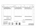
Drawing 4501-451 as you review this material.
CARRIER BOARD OVERVIEW
The carrier board is a VMEbus slave board providing up to four
industry standard IP module interfaces for the AVME9660 and two
IP module interfaces for the AVME9630. The carrier board’s
VMEbus interface allows an intelligent single board computer
(VMEbus Master) to control and communicate with electronic
devices that are external to the VMEbus card cage. The external
electronic hardware is linked to the carrier board via ribbon cable
which mates with the IP field connections of the carrier board. The
electronic link from the field I/O connections to the carrier board is
made via the IP module selected for your specific application.
Interrupt Configuration Example
1. Clear the global interrupt enable bit in the Carrier Board Status
Register by writing a "0" to bit 3.
2. Write interrupt vector to the location specified on the IP and
perform any other IP specific configuration required - do for
each supported IP interrupt request.
3. Write to the Interrupt Level Register to program the desired
interrupt level per bits 2,1,0.
4. Write “1” to the IP Interrupt Clear Register corresponding to the
desired IP interrupt request(s) being configured.
5. Write “1” to the IP Interrupt Enable Register bits corresponding
to the IP interrupt request to be enabled.
6. Enable interrupts from the carrier board by writing a "1" to bit 3
(global interrupt enable bit) in the Carrier Board Status Register.
To facilitate easy connection of external devices to the IP field
I/O pins of the carrier board, optional Termination Panels are
available. A ribbon cable connects a 50 pin IP field I/O connector on
the carrier board to the Termination Panel. At the Termination Panel
field I/O signals are connected to a 50 position terminal block via
screw clamps. The AVME9660 contains four IP modules and thus
200 I/O connections are provided on the A, B, C, and D connectors.
The AVME9630 contains two IP modules and provides 100 I/O
connections on the A and B connectors.
Sequence of Events For an Interrupt
1. The IP asserts an interrupt request to the carrier board (asserts
IntReq0* or IntReq1*).
2. The AVME9630/9660 carrier board acts as an interrupter in
making the VMEbus interrupt request (asserts IRQx*)
corresponding to the IP interrupt request.
3. The VMEbus host (interrupt handler) asserts IACK* and the
level of the interrupt it is seeking on A01-A03.
4. When the asserted VMEbus IACKIN* signal (daisy-chained) is
passed to the AVME9630/9660, the carrier board will check if
the level requested matches that specified by the host. If so, the
carrier board will assert the IntSel* line to the appropriate IP
together with (carrier board generated) address bit A1 to select
which interrupt request is being processed (A1 low corresponds
to IntReq0*; A1 high corresponds to IntReq1*).
5. The IP puts the appropriate interrupt vector on the local data bus
(D00-D07 if an D08 (O) interrupter or D00-D15 if a D16
interrupter), and asserts Ack* to the carrier board. The carrier
board passes this along to the VMEbus (D08 [O] or D16) and
asserts DTACK*.
6. The host uses the vector to point at which interrupt handler to
execute and begins its execution.
7. Example of Generic Interrupt Handler Actions:
A. Disable the interrupting IP by writing a "0" to the appropriate
bit in the IP Interrupt Enable Register.
B. Take any IP specific action required to remove the interrupt
request at its source.
C. Clear the interrupting IP by writing a "1" to the appropriate
bit in the IP Interrupt Clear Register.
The VMEbus and IP module logic commons have a direct
electrical connection (i.e., they are not electrically isolated).
However, the field I/O connections can be isolated from the VMEbus
if an IP module that provides this isolation (between the logic and
field side) is utilized. A wide variety of IP modules are currently
available (from Acromag and other vendors) that allow interface to
many external devices for both digital and analog I/O applications.
VMEbus Interface
The carrier board’s VMEbus interface is used to program and
monitor and carrier board’s registers for configuration and control of
the board’s documented modes of operation (see section 3). In
addition, the VMEbus interface is also used to communicate with
and control external devices that are connected to an IP module’s
field I/O signals (assuming an IP module is present on the carrier
board).
The VMEbus interface is implemented in the logic of the carrier
board’s Field Programmable Gate-Array (FPGA). The FPGA
implements VMEbus specification revision C.1 as an interrupting
slave including the following data transfers types.
A16, D16/D08(O)
Carrier Register Short I/O Access
•
A16, D16/D08(O)
IP Module ID Space
•
A16, D16/D08(EO)
IP Module I/O Space
•
A24, D16/D08(EO)
IP Module Memory Space
•
- 11 -
INDUSTRIAL I/O PACK SERIES AVME9630/9660
VMEbus 3U/6U CARRIER BOARDS
___________________________________________________________________________________________
The carrier board’s VMEbus data transfer rates are typically:
500ns for accesses to the carrier board registers.
•
750ns for data transfers to the IP modules (assuming 0 wait
•
states on IP).
similar length PC board trace lengths are employed to minimize
clock skew between the IP modules.
The carrier board’s FPGA monitors the base address jumper
setting which is jumperable on 1K byte boundaries in the VMEbus
Short I/O (A16) Address Space. When the selected base address
matches the (A16) address provided by the VMEbus master, the
FPGA controls and implements the required bus transfer allowing
communication with the carrier board’s registers or IP modules.
An IP read or write cycle is carried out via a VMEbus A24 or
A16 data transfer. The data transfer starts when the VMEbus Data
Strobe 0 (DS0*) goes active and ends when the carrier board drives
Data Transfer Acknowledge (DTACK*) active back to the VMEbus
master. The carrier board typically has a 750ns IP module data
transfer cycle time.
Carrier Board Registers
A typical IP module data transfer cycle is described here,
starting with DS0* going active. DS0* is sampled on the rising edge
of the system 16MHz clock edge after it goes active. All operations
are then synchronized to the IP 8MHz clock as required by the IP
module specification. Thus, typically three 8MHz clock cycles later,
an IP select line goes active (IOSEL*, IDSEL*, MEMSEL*, or
INTSEL*). With no IP wait states, an active IP Acknowledge (ACK*)
signal is driven active by the IP on the next rising edge of the 8MHz
clock. The carrier board samples ACK* one clock cycle later and
then asserts DTACK* active ending the VMEbus data transfer. The
carrier board releases the select line (IOSEL*, IDSEL*, MEMSEL*,
or INTSEL*) on the first rising edge of the 8MHz clock cycle after
DS0* goes inactive.
Timing Diagram
IP Read and Write Cycle Timing
The carrier board registers (presented in section 3) are
implemented in the logic of the carrier board’s FPGA. An outline of
the functions provided by the carrier board registers include:
Software reset can be issued to reset the FPGA Logic and all
•
IP modules present on the carrier board via the Status
Register.
Monitoring the error signal received from each IP module is
•
possible via the IP Error Register.
Configuration of VMEbus A24 standard address space for
•
optional Memory Space on each IP module is possible.
Memory Space access to the IP modules can be individually
enabled via the IP Memory Enable Register. The base
address and address range (size) is programmed via carrier
registers IP_A, IP_B, IP_C, and IP_D Memory Base
Address & Size Registers. The address size can be
selected from 1M, 2M, 4M, or 8M bytes.
Enabling of VMEbus interrupt requests from each IP module
•
via the IP Interrupt Enable Register is possible. The desired
VMEbus interrupt level desired can be set (via the Interrupt
Level Register), and pending interrupts can be monitored and
cleared via carrier registers IP Interrupt Pending and IP
Interrupt Clear Registers.
Lastly, pending interrupts can be globally monitored and
•
released to the VMEbus via the Status Register.
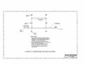
CLK 16MHz
CLK 8MHz
DS0*
IOSEL*
ACK*
DTACK*
IP Logic Interface
Note that the select line (IOSEL*, IDSEL*, MEMSEL* or
INTSEL*) is held active a short time after DTACK* is issued.
However, the IP module should not expect data to be held after
ACK* is detected by the carrier board in a data write cycle.
The IP logic interface is also implemented in the logic of the
carrier board’s FPGA. The carrier board implements revision 0.7.1
Industrial I/O Pack logic interface specification and includes four IP
logic interfaces on an AVME9660 and two interfaces on an
AVME9630 carrier. The VMEbus address and data lines are linked
to the address and data of the IP logic interface. This link is
implemented and controlled by the carrier board’s FPGA.
If a select line (IOSEL*, IDSEL*, INTSEL*, or MEMSEL*) is
driven active to an IP module and the IP module does not return
ACK* active, then DTACK* will also not be generated by the carrier
board. This will cause a bus transfer time-out error and the VMEbus
system may need to be reset. In addition, the carrier board will
remain in a state waiting for ACK* from the IP. To take it out of this
state, a software reset can be issued.
The VMEbus to IP logic interface link allows a VMEbus master
to :
Access up to 32 ID Space bytes for IP module identification via
•
D08(O) data transfers using VMEbus A16 short address
space.
Access up to 128 I/O Space bytes of IP data via D16/D08(EO)
•
data transfers using VMEbus A16 short address space.
Access up to 8Mbytes of IP data mapped to Memory Space via
•
D16 or D08(EO) transfers using VMEbus A24 standard
address space.
Respond to two IP module interrupt requests per IP with
•
software programmable VMEbus interrupt levels.
When an IP module places data on the bus, for all data read
cycles, any undriven data lines are read by the VMEbus as high
because of pull-up resisters on the carrier board’s data bus.
VME Interrupter
Interrupts are initiated from an interrupting IP module. However,
the carrier board will only pass an interrupt generated by an IP
module to the VMEbus if the carrier board has been first enabled for
interrupts. Each IP module can initiate two interrupts which can be
individually enabled on the carrier board. After interrupts are
enabled on the carrier board via the Interrupt Enable Register (see
section 3 for programming details), an IP generated interrupt is
recognized by the carrier board and is recorded in the carrier board’s
Interrupt Pending Register.
Carrier Board Clock Circuitry
The VMEbus 16MHz system clock is divided down by the
FPGA to obtain the IP module 8MHz clock signals. Separate IP
clocks are driven to each IP module. All clock lines include series
damping resistors to reduce clock overshoot and undershoot, and
- 12 -
INDUSTRIAL I/O PACK SERIES AVME9630/9660
VMEbus 3U/6U CARRIER BOARDS
___________________________________________________________________________________________
5.0 SERVICE AND REPAIR
A carrier board pending interrupt will cause the board to release
the interrupt to the VMEbus provided the Global Interrupt Enable bit
of the carrier’s Status Register has been enabled (see section 3 for
programming details).
SERVICE AND REPAIR ASSISTANCE
Surface-Mounted Technology (SMT) boards are generally
difficult to repair. It is highly recommended that a non-functioning
board be returned to Acromag for repair. The board can be
damaged unless special SMT repair and service tools are used.
Further, Acromag has automated test equipment that thoroughly
checks the performance of each board. When a board is first
produced and when any repair is made, it is tested, placed in a burnin room at elevated temperature, and retested before shipment.
The carrier board releases the interrupt to the VMEbus by
asserting the interrupt request level as pre-programmed in the
carrier’s Interrupt Level Register. The carrier board’s interrupt logic
then monitors the VMEbus Interrupt Acknowledge Input (IACKIN*)
signal.
An active IACKIN* signal, detected by the carrier board, is either
passed to Interrupt Acknowledge Output (IACKOUT*) or consumed
by the carrier board. IACKIN* is passed to IACKOUT* if the
VMEbus interrupt level does not match that programmed into the
carrier’s Interrupt Level Register. If a match is detected, the carrier
board responds to the interrupt by consuming IACKIN*.
Please refer to Acromag's Service Policy Bulletin or contact
Acromag for complete details on how to obtain parts and repair.
PRELIMINARY SERVICE PROCEDURE
The carrier board also responds to an interrupt by driving IP
Interrupt Select (INTSEL*) active to the IP that generated the
interrupt provided only one interrupt has been issued. If two or more
interrupts occur at the same time, then INTSEL* is driven active to
the IP with the highest priority (IP A int0 has the highest priority, IP
D Int1 has the lowest priority, see section 3 for more detail). The IP
module responds by placing the interrupt vector on the data bus and
asserts ACK* active. The carrier then asserts DTACK* active, and
the VMEbus master responds by executing the code at the address
of the interrupt vector.
Before beginning repair, be sure that all of the procedures in
Section 2, Preparation For Use, have been followed. Also, refer to
the documentation of your carrier board to verify that it is correctly
configured. Replacement of the carrier and/or IP with one that is
known to work correctly is a good technique to isolate a faulty board.
CAUTION: POWER MUST BE TURNED OFF BEFORE
REMOVING OR INSERTING BOARDS
The user written interrupt routine should include code to clear
the carrier board’s pending interrupt via the carrier’s Interrupt Clear
Register (see section 3) since the interrupt release mechanism is
type Release on Register Access (RORA). In addition, the IP
module may need similar attention (see your IP module
documentation).
Acromag’s Applications Engineers can provide further technical
assistance if required. When needed, complete repair services are
also available from Acromag.
6.0 SPECIFICATIONS
Power Failure Monitor
GENERAL SPECIFICATIONS
The carrier board contains a 5 volts undervoltage monitoring
circuit which provides a reset to the IP modules when the 5 volt
power drops below 4.27 volts typical / 4.15 volts minimum. This
circuitry is implemented per the Industrial I/O Pack specification.
Operating Temperature...................0 to +70°C
-40 to +85°C (E Versions)
Note that visual LED performance
may be degraded below -20°C.
Relative Humidity............................5-95% non-condensing
Storage Temperature.....................-55 to +100°C
Assess LEDs and Pulse Stretcher Circuitry
An LED display and pulse stretcher circuit is dedicated to each
IP module for indication of a data transfer to/from the corresponding
IP module. An IP acknowledged data transfer activates the pulse
stretcher circuit. The pulse stretcher’s circuit is programmed to
illuminate the LED for a duration of 0.1 seconds typical.
Physical Configuration....................AVME9630 (3U)
Length......................................3.937 inches (100.0 mm)
Width.......................................6.299 inches (160.0 mm)
Board Thickness......................0.062 inches (1.59 mm)
Max Component Height............0.550 inches (13.97 mm)
Recommended Card Spacing..0.800 inches, (20.32mm)
Physical Configuration....................AVME9660 (6U)
Length......................................9.187 inches (233.3 mm)
Width........................................6.299 inches (160.0 mm)
Board Thickness.......................0.062 inches (1.59 mm)
Max Component Height............0.550 inches (13.97 mm)
Recommended Card Spacing...0.800 inches, (20.32mm)
Connectors:
P1 (VMEbus)............................DIN 41612 96-pin Type C,
Level II
P2 (VMEbus)............................Not Used.
A-D (Carrier Field I/O)..............50-pin Male Header x2 stacked
“condo type” 3M 3433-D303
with ejector latches(AVME9660)
A, B (Carrier Field I/O):.............50-pin Male Headers.
No ejector latches(AVME9630)
Power Supply Filters
Power line filters are dedicated to each IP module for filtering of
the +5, +12, and -12 volt supplies. The power line filters are a T
type filter circuit comprising ferrite bead inductors and a feed-thru
capacitor. The filters provide improved noise performance as is
required on precision analog IP modules. Specifically, the filters are
typically capable of over 40dB of insertion loss for undesirable noise
and oscillations in the 100MHz frequency range and over 20dB of
insertion loss for noise and oscillations in the 10MHz frequency
range.
- 13 -
INDUSTRIAL I/O PACK SERIES AVME9630/9660
VMEbus 3U/6U CARRIER BOARDS
___________________________________________________________________________________________
VMEbus Access Time...................500nS Typical (all carrier board
registers); measured from the
falling edge of DSx* to the falling
edge of DTACK*.
750nS Typical (IP registers with
no wait states). See IP
specifications for information on
wait states. IP register access
time will increase by the number
of wait states multiplied by
125nS (the period of the 8 Mhz
clock).
A: Right angle pins
3M 2550-5002UB (or equiv.)
B: Straight pins,
3M 2550-6002UB (or equiv.)
P7-P10 (IP Field I/O)................50-pin male plug header (AMP
173280-3 or equivalent).
P9,P10 are not present on
AVME9630 (E).
P11-P14 (IP Logic Interface)...50-pin male plug header (AMP
173280-3 or equivalent).
P13,P14 are not present on
AVME9630 (E).
Power:
Board power requirements are a function of the installed IP
modules. This specification lists currents for the carrier boards
only. The carrier boards individually filter and provide +5V,
+12V and -12V power to each IP from the VMEbus. Note that
the VMEbus standard does not support +15V and -15V
supplies, but the carrier boards are designed to handle these if
needed for unique situations.
VMEbus Address Modifier Codes:
Short I/O Space.............................Base address is hardware jumper
selectable. Occupies 1K byte.
Responds to both address
modifiers 29H & 2DH in the
VMEbus short I/O space for
carrier board registers and IP I/O
and ID PROM spaces.
Standard Address Space...............Responds to both address
modifiers 39H & 3DH in the
VMEbus standard address space
when such accesses to IP
memory are enabled via
programmable registers on the
carrier board. Base addresses
and sizes of IP memory are
programmable from 1M to 8M
bytes.
Interrupts.......................................Creates I(1-7) programmable
request levels (up to two requests
sourced from each IP).
D16/D08(O) interrupter (interrupt
vectors come from IP modules).
Carrier registers for control &
status monitoring. Interrupt
release mechanism is Release
On Register Access (RORA)
type.
The power supply filters are typically capable of over 40dB of
insertion loss for undesirable noise and oscillations in the
100MHz frequency range and over 20dB of insertion loss for
noise and oscillations in the 10MHz frequency range.
The power failure monitor circuit provides a reset to IP modules
when the 5 volt power drops below 4.27 volts typically / 4.15
volts minimum.
Currents specified are for the carrier board only, add the IP
module currents for the total current required from each supply.
+5 Volts (±5%)........................AVME9630 (E) 210mA, Typical
275mA, Maximum.
AVME9660 (E) 210mA, Typical
275mA, Maximum.
+12 Volts (±5%) or
+15 Volts (±5%).......................0mA (Not Used)
-12 Volts (±5%) or
-15 Volts (±5%)........................0mA (Not Used)
INDUSTRIAL I/O PACK COMPLIANCE
Specification.................................This device meets or exceeds all
written Industrial I/O Pack
specifications per revision 0.7.1.
Electrical/Mechanical Interface.....AVME9630 (E) supports two
single-size IP modules (A-B), or
one double-size. 32-bit IP
modules are Not Supported.
AVME9660 (E) supports four
single-size IP modules (A-D), or
two double-size. 32-bit IP
modules are Not Supported.
I/O Space.....................................A16/D16 or D08(EO);
supports 128 byte values per IP.
ID Space.......................................A16/D08(O); supports 32 bytes
per IP (consecutive odd-byte
addresses). D16 is also
supported with pull-ups on the
carrier board holding the upper
8-bits high.
Memory Space.............................A24/D16 or D08(EO); supports 1M
to 8M bytes per IP module.
Non-Isolated....................................VMEbus and IP module logic
commons have a direct electrical
connection. As such, unless the
IP module provides isolation
between the logic and field side,
the field I/O connections are not
isolated from the VMEbus.
LED illuminate duration ..................0.1 second, typical
VMEbus COMPLIANCE
Specification..................................This device meets or exceeds all
written VME specifications per
revision C.1 dated October 1985,
IEC 821-1987 and IEEE
1014-1987.
Data Transfer Bus..........................A24/A16:D16/D08 (EO) DTB
slave; supports Read-ModifyWrite cycles.
- 14 -
INDUSTRIAL I/O PACK SERIES AVME9630/9660
VMEbus 3U/6U CARRIER BOARDS
___________________________________________________________________________________________
Interrupts.....................................Supports two interrupt requests per
IP and interrupt acknowledge
cycles, D16/D08(O).
- 15 -
INDUSTRIAL I/O PACK SERIES AVME9630/9660
VMEbus 3U/6U CARRIER BOARDS
___________________________________________________________________________________________
APPENDIX
TRANSITION MODULE: MODEL TRANS-GP
CABLE: MODEL 5025-550-x (Non-Shielded)
MODEL 5025-551-x (Shielded)
Type: Transition module for AVME9630/9660 boards.
Application: To repeat field I/O signals of IP modules A through D
for rear exit from VME card cages. This module is available for
use in card cages which provide rear exit for I/O connections via
transition modules (transition modules can only be used in card
cages specifically designed for them). It is a double-height
(6U), single-slot module with front panel hardware adhering to
the VMEbus mechanical dimensions, except for shorter printed
circuit board depth. Connects to Acromag termination panel
5025-552 from the rear of the card cage, and to
AVME9630/9660 boards within card cage, via flat 50-pin ribbon
cable (cable Model 5025-550-X or 5025-551-X).
Schematic and Physical Attributes: See Drawing 4501-465.
Field Wiring: 100-pin header (male) connectors (3M 3433-D303 or
equivalent) employing long ejector latches and 30 micron gold in
the mating area (per MIL-G-45204, Type II, Grade C).
Connects to Acromag termination panel 5025-552 from the rear
of the card cage via flat 50-pin ribbon cable (cable Model
5025-550-X or 5025-551-X).
Connections to AVME9630/9660: 50-pin header (male) connectors
(3M 3433-1302 or equivalent) employing long ejector latches
and 30 micron gold in the mating area (per MIL-G-45204, Type
II, Grade C). Connects to AVME9630/9660 boards within the
card cage via flat 50-pin ribbon cable (cable Model 5025-550-X
or 5025-551-X).
Mounting: Transition module is inserted into a 6U-size, single-width
slot at the rear of the VMEbus card cage.
Printed Circuit Board: Six-layer, military-grade FR-4 epoxy glass
circuit board, 0.063 inches thick.
Operating Temperature: -40 to +85°C.
Storage Temperature: -55°C to +105°C.
Shipping Weight: 1.25 pounds (0.6Kg) packed.
Type: Flat Ribbon Cable, 50-wires (female connectors at both
ends). The ‘-x’ suffix designates the length in feet (12 feet
maximum). Choose shielded or unshielded cable according to
model number. The unshielded cable is recommended for
digital I/O, while the shielded cable is recommended for
optimum performance with precision analog I/O applications.
Application: Used to connect Model 5025-552 termination panel to
the AVME9630/9660 non-intelligent carrier board A-D
connectors (Both have 50-pin connectors).
Length: Last field of part number designates length in feet (userspecified, 12 feet maximum). It is recommended that this length
be kept to a minimum to reduce noise and power loss.
Cable: 50-wire flat ribbon cable, 28 gage. Non-Shielded cable
model uses Acromag Part 2002-211 (3M Type C3365/50 or
equivalent). Shielded cable model uses Acromag Part 2002-261
(3M Type 3476/50 or equivalent).
Headers (Both Ends): 50-pin female header with strain relief.
Header - Acromag Part 1004-512 (3M Type 3425-6600 or
equivalent). Strain Relief - Acromag Part 1004-534 (3M Type
3448-3050 or equivalent).
Keying: Headers at both ends have polarizing key to prevent
improper installation.
Schematic and Physical Attributes: For Non-Shielded cable model,
see Drawing 4501-462. For Shielded cable model, see Drawing
4501-463.
Shipping Weight: 1.0 pound (0.5Kg), packed.
TERMINATION PANEL: MODEL 5025-552
Type: Termination Panel For AVME9630/9660 Boards
Application: To connect field I/O signals to the Industrial I/O Pack
(IP). Termination Panel: Acromag Part 4001-040 (Phoenix
Contact Type FLKM 50). The 5025-552 termination panel
facilitates the connection of up to 50 field I/O signals and
connects to the AVME9630/9660 3U/6U non-intelligent carrier
boards (A-D connectors only) via a flat ribbon cable (Model
5025-550-x or 5025-551-x). The A-D connectors on the carrier
board connect the field I/O signals to the P2 connector on each
of the Industrial I/O Pack modules. Field signals are accessed
via screw terminal strips. The terminal strip markings on the
termination panel (1-50) correspond to P2 (pins 1-50) on the
Industrial I/O Pack (IP). Each Industrial I/O Pack (IP) has its
own unique P2 pin assignments. Refer to the IP module manual
for correct wiring connections to the termination panel.
Schematic and Physical Attributes: See Drawing 4501-464.
Field Wiring: 50-position terminal blocks with screw clamps. Wire
range 12 to 26 AWG.
Connections to AVME9630/9660: P1, 50-pin male header with
strain relief ejectors. Use Acromag 5025-550-x or 5025-551-x
cable to connect panel to VME board. Keep cable as short as
possible to reduce noise and power loss.
Mounting: Termination panel is snapped on the DIN mounting rail.
Printed Circuit Board: Military grade FR-4 epoxy glass circuit board,
0.063 inches thick.
Operating Temperature: -40°C to +100°C.
Storage Temperature: -40°C to +100°C.
Shipping Weight: 1.25 pounds (0.6kg) packed.
- 16 -