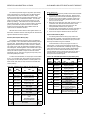
1
Series IP440 Industrial I/O Pack
32-Channel Isolated Digital Input Module
With Interrupts
USER’S MANUAL
ACROMAG INCORPORATED
30765 South Wixom Road
P.O. BOX 437
Wixom, MI 48393-7037 U.S.A.
Tel: (248) 624-1541
Fax: (248) 624-9234
Copyright 1996, Acromag, Inc., Printed in the USA.
Data and specifications are subject to change without notice.
8500-551-E01D006
SERIES IP440 INDUSTRIAL I/O PACK
32-CHANNEL ISOLATED DIGITAL INPUT MODULE
___________________________________________________________________________________________
IMPORTANT SAFETY CONSIDERATIONS
The information contained in this manual is subject to change
without notice. Acromag, Inc. makes no warranty of any kind with
regard to this material, including, but not limited to, the implied
warranties of merchantability and fitness for a particular purpose.
Further, Acromag, Inc. assumes no responsibility for any errors that
may appear in this manual and makes no commitment to update, or
keep current, the information contained in this manual. No part of
this manual may be copied or reproduced in any form, without the
prior written consent of Acromag, Inc.
Table of Contents
1.0 GENERAL INFORMATION...............................................
KEY IP440 FEATURES.....................................................
INDUSTRIAL I/O PACK INTERFACE FEATURES..........
SIGNAL INTERFACE PRODUCTS..................................
INDUSTRIAL I/O PACK SOFTWARE LIBRARY..............
2.0 PREPARATION FOR USE................................................
UNPACKING AND INSPECTION.....................................
CARD CAGE CONSIDERATIONS...................................
BOARD CONFIGURATION..............................................
CONNECTORS.................................................................
IP Field I/O Connector (P2)............................................
Noise and Grounding Considerations.............................
IP Logic Interface Connector (P1)..................................
3.0 PROGRAMMING INFORMATION....................................
ADDRESS MAPS..............................................................
Standard (Default) Mode Memory Map...........................
Enhanced Mode Memory Map........................................
REGISTER DEFINITIONS................................................
THE EFFECT OF RESET.................................................
IP440 PROGRAMMING....................................................
Basic Input Operation.....................................................
Enhanced Operating Mode.............................................
Event Sensing................................................................
Change-Of-State Detection............................................
Debounce Control..........................................................
Interrupt Generation.......................................................
Programming Example...................................................
4.0 THEORY OF OPERATION...............................................
IP440 OPERATION...........................................................
LOGIC/POWER INTERFACE...........................................
5.0 SERVICE AND REPAIR....................................................
SERVICE AND REPAIR ASSISTANCE...........................
PRELIMINARY SERVICE PROCEDURE.........................
6.0 SPECIFICATIONS.............................................................
GENERAL SPECIFICATIONS..........................................
INPUTS..............................................................................
INDUSTRIAL I/O PACK COMPLIANCE...........................
It is very important for the user to consider the possible adverse
effects of power, wiring, component, sensor, or software failures in
designing any type of control or monitoring system. This is
especially important where economic property loss or human life is
involved. It is important that the user employ satisfactory overall
system design. It is agreed between the Buyer and Acromag, that
this is the Buyer's responsibility.
Page
2
2
3
3
3
3
3
4
4
4
4
5
5
5
5
6
6
7
11
11
11
11
11
12
12
12
12
13
13
14
14
14
14
14
14
15
15
APPENDIX.........................................................................
CABLE: MODEL 5025-550. & 5025-551...........................
CABLE: MODEL 5029-900................................................
TERMINATION PANEL: MODEL 5025-552.....................
TERMINATION PANEL: MODEL 5029-910.....................
TRANSITION MODULE: MODEL TRANS-GP.................
15
15
15
16
16
16
DRAWINGS
4501-434 IP MECHANICAL ASSEMBLY.........................
4501-593 IP440 FIELD CONNECTIONS.........................
4501-603 IP440/445 LOOPBACK CONNECTIONS........
4501-594 IP440 BLOCK DIAGRAM.................................
4501-462 CABLE 5025-550 (NON-SHIELDED)..............
4501-463 CABLE 5025-551 (SHIELDED)........................
4501-464 TERMINATION PANEL 5025-552...................
4501-465 TRANSITION MODULE TRANS-GP...............
Page
17
17
18
18
19
19
20
20
-2-
1.0 GENERAL INFORMATION
The Industrial I/O Pack (IP) Series IP440 module provides 32
channels of isolated digital inputs for interfacing to the VMEbus or
ISAbus, according to your carrier board. Four units may be mounted
on a single carrier board to provide up to 128 inputs per system slot.
Inputs of this module are bipolar and can be used to sense
positive or negative voltages in 3 ranges according to the model:
MODEL
IP440-1
IP440-2
IP440-3
MODEL
IP440-X
IP440-XE
INPUT RANGE
± 4V to ±18V DC or AC peak
± 16 to ±40V DC or AC peak
± 38 to ±60V DC or AC peak
THRESHOLD
± 4V Maximum
± 16V Maximum
± 38V Maximum
OPERATING TEMPERATURE RANGE
0 to +70°C
-40 to +85°C
The inputs normally function as independent input level
detectors without interrupts. However, each input line includes builtin event sense circuitry with programmable polarity, debounce, and
interrupt support. Inputs also include hysteresis for increased noise
immunity. The IP440 utilizes state of the art Surface-Mounted
Technology (SMT) to achieve its wide functionality and is an ideal
choice for a wide range of industrial I/O applications that require a
high-density, highly reliable, high-performance interface at a low
cost.
KEY IP440 FEATURES
• High Channel Count - Provides programmable monitor and
control of 32 optically-isolated input points. Four units mounted
on a carrier board provide 128 isolated input points in a single
VMEbus or ISAbus (PC/AT) system slot.
• High-Speed/0 Wait States - No wait states are required for all
read/write cycles (all cycles complete in 250ns) and hold states
are supported.
• Wide Range Bipolar Input Voltage - Three model ranges
provide interface capability for bipolar voltages from ±4 to ±60V
DC or AC peak (see Specifications section).
• Optically Isolated - Individual bipolar opto-couplers provide
isolation. There are four groups (ports) of 8 channels each
which include separate port commons to ensure port-to-port
isolation. Individual ports are isolated from each other and from
the logic.
• Programmable Polarity Event Interrupts - Interrupts are
software programmable for positive (low-to-high) or negative
(high-to-low) input level transitions on all 32 channels. Using
two channels per input, change-of-state transitions may also be
configured.
SERIES IP440 INDUSTRIAL I/O PACK
32-CHANNEL ISOLATED DIGITAL INPUT MODULE
___________________________________________________________________________________________
•
•
•
•
•
•
Input Hysteresis - Isolated inputs include hysteresis for
increased noise immunity.
Programmable Debounce - The event sense input circuitry
includes programmable debounce times for all 32 channels.
Debounce time is the duration of time that must pass before
the input transition is recognized as valid at the ASIC input.
This helps prevent false events and increases noise immunity.
Reverse Polarity Protection - Bipolar inputs are not polarized
and are inherently reverse polarity protected.
No Configuration Jumpers or Switches - All configuration is
performed through software commands with no internal
jumpers to configure or switches to set.
ASIC Based Monitor - State of the art ASIC (Application
Specific Integrated Circuit from Ziatech Corporation) provides
the 32 channel input and event functionality.
Loopback Compatible with IP445 Output Module - The
field side P2 pinouts of this model are directly compatible with
those of the Acromag Model IP445 32-Channel Digital Output
Module for direct closed-loop monitoring of the output states.
The IP440 also shares the same P2 pinout used on the
Acromag non-isolated IP400 40 Channel Input Module, IP405
40-Channel Output Module, and IP408 32-Channel I/O
Module, for channels 0-31. Likewise, this model may interface
with industry standard I/O panels, termination panels, and relay
racks when used with an Acromag Model 5025-655 I/O
Adaptor Card. However, since relay racks generally provide
isolation, it may be more efficient to interface with them using
the non-isolated IP400 input module.
The unshielded cable is recommended for digital I/O, while the
shielded cable is recommended for optimum performance with
precision analog I/O applications. The “-X” suffix of the model
number denotes the length in feet.
Model 5029-900 APC8600 High-Density Cable: A 36-inch long
interface cable that mates the high-density (25mil pitch) 50-pin
I/O connectors of the APC8600 PCbus carrier board, to the
high-density connectors on the APC8600 Termination Panel
(described below).
Termination Panels:
Model 5025-552: A DIN-rail mountable panel that provides 50
screw terminals for universal field I/O termination. Connects to
Acromag AVME9630/9660, or other compatible carrier boards,
via flat 50-pin ribbon cable (Model 5025-550-X or 5025-551-X).
Model 5029-910 APC8600 High-Density-to-Screw-Terminal
Termination Panel: This panel converts the high-density ribboncable connectors coming from the APC8600 carrier board
(Acromag cable Model 5029-900) to screw terminals, for directwired interfaces.
Transition Module:
Model TRANS-GP: This module repeats field I/O connections
of IP modules A through D for rear exit from a VMEbus card
cage. It is available for use in card cages which provide rear exit
for I/O connections via transition modules (transition modules
can only be used in card cages specifically designed for them).
It is a double-height (6U), single-slot module with front panel
hardware adhering to the VMEbus mechanical dimensions,
except for shorter printed circuit board depth. It connects to
Acromag Termination Panel 5025-552 from the rear of the card
cage, and to AVME9630/9660 boards within the card cage, via
flat 50-pin ribbon cable (cable Model 5025-550 or 5025-551).
INDUSTRIAL I/O PACK INTERFACE FEATURES
High density - Single-size, industry standard, IP module
footprint. Four units mounted on a carrier board provide up to
128 isolated input points in a single system slot. Both VMEbus
and ISAbus (PC/AT) carriers are supported.
• Local ID - Each IP module has its own 8-bit ID PROM which is
accessed via data transfers in the "ID Read" space.
• 8-bit I/O - Port register Read/Write is performed through 8-bit
data transfer cycles in the IP module I/O space.
• High Speed with No Wait States - Access times for all data
transfer cycles are described in terms of "wait" states--0 wait
states are required for all read and write operations of this
model. See Specifications section for detailed information.
•
INDUSTRIAL I/O PACK SOFTWARE LIBRARY
Acromag provides an Industrial I/O Pack Software Library
diskette (Model IPSW-LIB-M03, MSDOS format) to simplify
communication with the board. Example software functions are
provided for both ISAbus (PC/AT) and VMEbus applications.
Software functions of the IP440 are shared by the IP470. All
functions are written in the “C” programming language and can be
linked to your application. For more details, refer to the
“README.TXT” file in the root directory on the diskette and the
“INFO440.TXT” file in the appropriate “IP470” subdirectory off of
“\VMEIP” or “\PCIP”, according to your carrier.
SIGNAL INTERFACE PRODUCTS
(See Appendix for more information on compatible products)
This IP module will mate directly to any industry standard IP
carrier board (including Acromag AVME9630/9660 3U/6U nonintelligent VMEbus carrier boards). Additionally, PC carrier boards
are also supported (see Acromag Model APC8600). A wide range
of other Acromag IP modules are also available to serve your signal
conditioning and interface needs.
2.0 PREPARATION FOR USE
Note: Since all connections to field signals are made through the
carrier board which passes them to the individual IP modules, you
should consult the documentation of your carrier board to ensure
compatibility with the following interface products.
UNPACKING AND INSPECTION
Upon receipt of this product, inspect the shipping carton for
evidence of mishandling during transit. If the shipping carton is
badly damaged or water stained, request that the carrier's agent be
present when the carton is opened. If the carrier's agent is absent
when the carton is opened and the contents of the carton are
damaged, keep the carton and packing material for the agent's
inspection.
Cables:
Model 5025-551-X (Shielded Cable), or Model 5025-550-X
(Non-Shielded Cable): A Flat 50-pin cable with female
connectors at both ends for connecting AVME9630/9660, or
other compatible carrier boards, to Model 5025-552 termination
panels.
-3-
SERIES IP440 INDUSTRIAL I/O PACK
32-CHANNEL ISOLATED DIGITAL INPUT MODULE
___________________________________________________________________________________________
P2 pin assignments are unique to each IP model (see Table 2.1)
and normally correspond to the pin numbers of the field I/O interface
connector on the carrier board (you should verify this for your carrier
board).
For repairs to a product damaged in shipment, refer to the
Acromag Service Policy to obtain return instructions. It is suggested
that salvageable shipping cartons and packing material be saved for
future use in the event the product must be shipped.
This board is physically protected with
packing material and electrically
protected with an anti-static bag during
shipment. However, it is recommended
that the board be visually inspected for
evidence of mishandling prior to applying
power.
Table 2.1: IP440 Field I/O Pin Connections (P2)
Pin Description
IN00
IN01
IN02
P
IN03
O
NC
R
IN04
T
IN05
IN06
0
IN07
ACOM
IN08
IN09
IN10
P
IN11
O
NC
R
IN12
T
IN13
IN14
1
IN15
BCOM
The board utilizes static-sensitive
components and should only be handled
at a static-safe workstation.
CARD CAGE CONSIDERATIONS
Refer to the specifications for loading and power requirements.
Be sure that the system power supplies are able to accommodate
the power requirements of the carrier board, plus the installed IP
modules, within the voltage tolerances specified.
IMPORTANT: Adequate air circulation must be provided to prevent
a temperature rise above the maximum operating temperature.
The dense packing of the IP modules to the carrier board
restricts air flow within the card cage and is cause for concern.
Adequate air circulation must be provided to prevent a temperature
rise above the maximum operating temperature and to prolong the
life of the electronics. If the installation is in an industrial
environment and the board is exposed to environmental air, careful
consideration should be given to air-filtering.
BOARD CONFIGURATION
Number
1
2
3
4
5
6
7
8
9
10
11
12
13
14
15
16
17
18
19
20
Pin Description
IN16
IN17
IN18
P
IN19
O
NC
R
IN20
T
IN21
IN22
2
IN23
CCOM
IN24
IN25
IN26
P
IN27
O
NC
R
IN28
T
IN29
IN30
3
IN31
DCOM
No Connection
No Connection
No Connection
No Connection
No Connection
No Connection
No Connection
No Connection
No Connection
No Connection
Number
21
22
23
24
25
26
27
28
29
30
31
32
33
34
35
36
37
38
39
40
41
42
43
44
45
46
47
48
49
50
Input channels of this module are divided into four ports of eight
channels each. Channels of a port share a common signal
connection with each other. Isolation is provided between ports and
between each port and the IP logic. With respect to interrupt
generation and events, event polarities may be defined as positive
(low-to-high), or negative (high-to-low) for individual nibbles (groups
of 4 input lines, or half ports). Change-of-State detection would
require 2 input channels--one detecting positive events, one
detecting negative events.
Power should be removed from the board when installing IP
modules, cables, termination panels, and field wiring. Refer to
Mechanical Assembly Drawing 4501-434 and your IP module
documentation for configuration and assembly instructions. Model
IP440 digital input boards have no hardware jumpers or switches to
configure.
CONNECTORS
P2 pinouts are arranged to be compatible with similar industry
models. This model is directly loopback compatible with the
Acromag Model IP445 Digital Output Module. Likewise, pin
assignments are identical to those of Acromag Model IP400 40Channel Digital Input Boards for channels 0-31. This model may
also interface with industry accepted I/O panels, termination panels,
and relay racks when used with the Acromag Model 5025-655 I/O
Adapter Card. Consult the factory for information on these and other
compatible products.
IP Field I/O Connector (P2)
P2 provides the field I/O interface connections for mating IP
modules to the carrier board. P2 is a 50-pin female receptacle
header (AMP 173279-3 or equivalent) which mates to the male
connector of the carrier board (AMP 173280-3 or equivalent). This
provides excellent connection integrity and utilizes gold-plating in the
mating area. Threaded metric M2 screws and spacers are supplied
with the module to provide additional stability for harsh environments
(see Mechanical Assembly Drawing 4501-434). The field and logic
side connectors are keyed to avoid incorrect assembly.
Refer to Drawing 4501-593 for example input connections. See
Drawing 4501-603 for loopback connections to Acromag Model
IP445 Output Modules. Drawing 4501-603 also gives an example of
how to interface the IP440-1 with open-drain TTL outputs signals.
-4-
SERIES IP440 INDUSTRIAL I/O PACK
32-CHANNEL ISOLATED DIGITAL INPUT MODULE
___________________________________________________________________________________________
Threaded metric M2 screws and spacers are supplied with the IP
module to provide additional stability for harsh environments (see
Drawing 4501-434 for assembly details). Field and logic side
connectors are keyed to avoid incorrect assembly.
Note that the inputs of this device are bipolar, and may be
connected in any direction with respect to the port common.
Further, do not confuse port commons with signal ground. For the
IP440, port common only infers that this lead is connected common
to the 8 inputs of the port (a separate port common for each port).
Likewise, the port commons of the IP440 input module and IP445
output module are normally not connected together for loopback
interconnection (see Drawing 4501-603).
3.0 PROGRAMMING INFORMATION
ADDRESS MAPS
Noise and Grounding Considerations
This board is addressable in the Industrial Pack I/O space to
control the configuration and status monitoring of 32 digital input or
event channels.
Input lines of the IP440 are optically isolated between the logic
and field input connections. Likewise, separate port commons
facilitate port-to-port isolation. Consequently, the field I/O
connections are isolated from the carrier board and backplane, thus
minimizing the negative effects of ground bounce, impedance drops,
and switching transients. However, care should be taken in
designing installations to avoid inadvertent isolation bridges, noise
pickup, isolation voltage clearance violations, equipment failure, or
ground loops.
This board operates in two modes: Standard Mode and
Enhanced Mode. Standard Mode provides digital input voltage
monitoring of 32 isolated signal lines. In Standard Mode, each input
line is configured as a simple input without interrupts. Data is read
from (or written to) one of eight groups (ports) as designated by the
address and read and write signals. The ASIC of this model is
capable of I/O, but this model is intended for input only. A Mask
Register is used to disable writes to I/O ports designed for input
only. Enhanced Mode includes the same functionality of Standard
Mode, but adds access to 32 additional event sense inputs
connected to each input point of ports 0-3. Individual inputs also
include selectable hardware debounce in Enhanced Mode. For
event sensing, the Enhanced Mode allows a specific input level
transition (High-to-Low, Low-to-High, or Change-of-State) to be
detected and optionally generate an interrupt.
IP Logic Interface Connector (P1)
Table 2.2: Standard Logic Interface Connections (P1)
Pin Description
GND
CLK
Reset*
D00
D01
D02
D03
D04
D05
D06
D07
D08
D09
D10
D11
D12
D13
D14
D15
BS0*
BS1*
-12V
+12V
+5V
GND
Number
1
2
3
4
5
6
7
8
9
10
11
12
13
14
15
16
17
18
19
20
21
22
23
24
25
Pin Description
GND
+5V
R/W*
IDSEL*
DMAReq0*
MEMSEL*
DMAReq1*
IntSel*
DMAck0*
IOSEL*
RESERVED
A1
DMAEnd*
A2
ERROR*
A3
INTReq0*
A4
INTReq1*
A5
STROBE*
A6
ACK*
RESERVED
GND
Number
26
27
28
29
30
31
32
33
34
35
36
37
38
39
40
41
42
43
44
45
46
47
48
49
50
Memory is organized and addressed in separate banks of eight
registers or ports (eight ports to a bank). The Standard Mode of
operation addresses the first group of 8 registers or ports (ports 0-3
for reading inputs, Ports 4, 5, & 6 which are not used on this model,
and Port 7 which is the Mask Register). The mask register is
included to mask writes to input points, since the input points of this
model are intended for input only, while the digital ASIC is capable of
output control. If the Enhanced Mode is selected, then 3 additional
banks of 8 registers are accessed to cover the additional
functionality in this mode (events, interrupts, and debounce). The
first bank of the Enhanced Mode (bank 0) is similar in operation to
the Standard Mode. The second bank (bank 1) provides event
sense and interrupt control. The third bank is used to configure the
debounce circuitry to be applied to input channels in the Enhanced
Mode. Two additional mode-independent registers are provided to
enable the interrupt request line, generate a software reset, and
store the interrupt vector.
The I/O space may be as large as 64, 16-bit words (128 bytes)
using address lines A1..A6, but the IP440 uses only a portion of this
space. The I/O space address map for the IP440 is shown in Table
3.1. Note the base address for the IP module I/O space (see your
carrier board instructions) must be added to the addresses shown to
properly access the I/O space. All accesses are performed on an 8bit byte basis (D0..D7).
An Asterisk (*) is used to indicate an active-low signal.
BOLD ITALIC Logic Lines are NOT USED by this IP Model.
P1 of the IP module provides the logic interface to the mating
connector on the carrier board. The pin assignments of P1 are
standard for all IP modules according to the Industrial I/O Pack
Specification (see Table 2.2). This connector is a 50-pin female
receptacle header (AMP 173279-3 or equivalent) which mates to the
male connector of the carrier board (AMP 173280-3 or equivalent).
This provides excellent connection integrity and utilizes gold-plating
in the mating area.
-5-
SERIES IP440 INDUSTRIAL I/O PACK
32-CHANNEL ISOLATED DIGITAL INPUT MODULE
___________________________________________________________________________________________
Notes (Table 3.1A):
1. Writes to these registers are possible, but this model is intended
for input only and writes should not be done. Writes to these
registers may be blocked via the Write Mask Register of Port 7.
2. The ASIC of this model is capable of a greater channel count,
but only 32 channels are used by this model, and as a result,
ports 4, 5, & 6 are not used.
3. Writing four unique bytes (07H, 0DH, 06H, and 12H) to port 7, in
consecutive order, will switch to Enhanced Mode. Do this
without doing any reads or writes to any other port, with
interrupts disabled, and after reset or power-up.
4. The upper 8 bits of these registers are not driven and pullups on
the carrier data bus will cause these bits to read high (1’s).
5. The IP will not respond to addresses that are "Not Used".
This manual is presented using the “Big Endian” byte ordering
format. Big Endian is the convention used in the Motorola 68000
microprocessor family and is the VMEbus convention. In Big
Endian, the lower-order byte is stored at odd-byte addresses. Thus,
byte accesses are done on odd address locations. The Intel x86
family of microprocessors use the opposite convention, or “Little
Endian” byte ordering. Little Endian uses even-byte addresses to
store the low-order byte. As such, use of this module on an ISAbus
(PC/AT) carrier board will require the use of the even address
locations to access the 8-bit data, while a VMEbus carrier will
require the use of odd address locations.
Note that some functions share the same register address. For
these items, the address lines are used along with the read and write
signals to determine the function required.
Enhanced Mode Memory Maps
The following table shows the memory maps used for the
Enhanced Mode of operation. Enhanced Mode includes the same
functionality of Standard Mode, but allows each input port’s event
sense input and debounce logic to be enabled.
Standard (Default) Mode Memory Map
The following table shows the memory map for the Standard
Mode of operation. This is the Default mode reached after power-up
or system reset. Standard Mode provides simple monitoring of 32
digital input lines without interrupts. Data is read from or written to
one of eight groups (ports) as designated by the address and read
and write signals. A Mask Register is used to disable writes to input
ports, since this model is intended for input only. That is, the ASIC
used by this model is capable of output, and since this model is
intended for input only, then each port (group of 8 input lines) must
be blocked (masked) from writes.
In Enhanced Mode, a memory map is given for each of 3
memory banks. The first memory bank (bank 0) has the same
functionality as the Standard Mode. Additionally, its port 7 register is
used to select which bank to access (similar to Standard Mode
where port 7 was used to select the Enhanced Mode). Bank 1
provides read/write access to the 32 event sense inputs. Bank 2
provides access to the registers used to control the debounce
circuitry of these event sense inputs.
Table 3.1B: IP440 R/W Space Address (Hex) Memory Map
EVEN
ODD
Base
MSB
LSB
Base
Addr+
D15
D08
D07
D00
Addr+
ENHANCED MODE, REGISTER BANK [0] DEFINITIONS:
READ4 - Port 0
00
1
Not Driven
Register IN00-IN07
01
READ4 -Port 1
02
Not Driven1
Register IN08-IN15
03
READ4 - Port 2
04
1
Not Driven
Register IN16-IN23
05
READ4 - Port 3
06
Not Driven1
Register IN24-IN31
07
READ/WRITE5 - Port 4
08
Not Driven1
NOT USED
09
READ/WRITE5 - Port 5
0A
Not Driven1
NOT USED
0B
READ/WRITE5 - Port 6
0C
1
Not Driven
NOT USED
0D
READ - Port 7
0E
Not Driven1
READ MASK REGISTER
(Also Current Bank Status)
0F
WRITE - Port 7
0E
1
Not Driven
WRITE MASK REGISTER
(Also Bank Select Register)
0F
To switch to Enhanced Mode, four unique bytes must be written
to port 7, in consecutive order, without doing any reads or writes to
any other port and with interrupts disabled. The data pattern to be
written is 07H, 0DH, 06H, and 12H, and this must be written after
reset or power-up.
Table 3.1A: IP440 R/W Space Address (Hex) Memory Map
EVEN
ODD
Base
MSB
LSB
Base
Addr+
D15
D08
D07
D00
Addr+
STANDARD MODE (DEFAULT) REGISTER DEFINITIONS:
READ1 - Port 0
00
Not Driven4
Register IN00-IN07
01
READ1 - Port 1
02
Not Driven4
Register IN08-IN/15
03
READ1 - Port 2
04
Register IN16-IN23
Not Driven4
05
READ1 - Port 3
06
4
Not Driven
Register IN24-IN31
07
READ/WRITE2 - Port 4
08
Not Driven4
NOT USED
09
READ/WRITE2 - Port 5
0A
Not Driven4
NOT USED
0B
READ/WRITE2 - Port 6
0C
Not Driven4
NOT USED
0D
READ/WRITE - Port 7
0E
Not Driven4
WRITE MASK REGISTER
AND
ENHANCED MODE
SELECT REGISTER3
0F
10
11
NOT USED5
↓
↓
7E
7F
-6-
SERIES IP440 INDUSTRIAL I/O PACK
32-CHANNEL ISOLATED DIGITAL INPUT MODULE
___________________________________________________________________________________________
Table 3.1B: IP440 R/W Space Address (Hex) Memory Map
EVEN
ODD
Base
MSB
LSB
Base
Addr+
D15
D08
D07
D00
Addr+
ENHANCED MODE, REGISTER BANK [1] DEFINITIONS:
READ - Port 0
00
Not Driven1
Event Sense Status Reg.
(Port 0 Input points 0-7)
01
WRITE - Port 0
00
1
Not Driven
Event Sense Clear Register
(Port 0 Input points 0-7)
01
READ - Port 1
02
Not Driven1
Event Sense Status Reg.
(Port 1 Input points 8-15)
03
WRITE - Port 1
02
Not Driven1
Event Sense Clear Register
(Port 1 Input points 8-15)
03
READ - Port 2
04
Not Driven1
Event Sense Status Reg.
(Port 2 Input points 16-23)
05
WRITE - Port 2
04
Not Driven1
Event Sense Clear Register
(Port 2 Input points 16-23)
05
READ - Port 3
06
Not Driven1
Event Sense Status Reg.
(Port 3 Input points 24-31)
07
WRITE - Port 3
06
Not Driven1
Event Sense Clear Register
(Port 3 Input points 24-31)
07
READ - Port 4
08
Not Driven1
NOT USED
09
WRITE - Port 4
08
Not Driven1
NOT USED
09
READ - Port 5
0A
Not Driven1
NOT USED
0B
WRITE - Port 5
0A
1
Not Driven
NOT USED
0B
READ - Port 6
0C
Not Driven1
Event Status for Ports 0-3
and Interrupt Status Reg.
0D
WRITE - Port 6
0C
1
Not Driven
Event Polarity Control
Register for Port 0-3
0D
READ - Port 7
0E
Not Driven1
Current Bank Status Reg.
0F
WRITE - Port 7
0E
1
Not Driven
Bank Select Register
0F
ENHANCED MODE, REGISTER BANK [2] DEFINITIONS:
READ/WRITE - Port 0
00
Not Driven1
Debounce Control Register
(for Ports 0-3)
01
READ/WRITE - Port 1
02
Not Driven1
Debounce Duration Reg. 0
(for Ports 0-3)
03
04
Not Driven1
NOT USED
05
WRITE ONLY - Port 3
06
Not Driven1
Debounce Clock Select
07
Port 4,5,6
08
09
Not Driven1
NOT USED2
↓
↓
0C
0D
READ/WRITE - Port 7
0E
1
Not Driven
Bank Status/Select Register
0F
Table 3.1B: IP440 R/W Space Address (Hex) Memory Map
EVEN
ODD
Base
MSB
LSB
Base
Addr+
D15
D08
D07
D00
Addr+
INDEPENDENT FIXED FUNCTION REGISTERS:
10
11
NOT USED2
↓
↓
1C
1D
READ/WRITE
1E
Not Driven1
Interrupt Enable Register
(Bit 0=1 enables INTREQ0)
& Software Reset Generator
(Bit 1=1 Generates Reset)
1F
20
21
NOT USED2
↓
↓
2C
2D
READ/WRITE
2E
Not Driven1
Interrupt Vector Register
2F
30
31
NOT USED2
↓
↓
7E
7F
Notes (Table 3.1B):
1. The upper 8 bits of these registers are not driven and pullups on
the carrier data bus will cause these bits to read high (1’s).
2. The IP will not respond to addresses that are "Not Used".
3. All Reads and Writes are 0 wait state.
4. Writes to these registers are possible, but this model is intended
for input only and writes should not be done. Writes to these
registers may be blocked via the Write Mask Register of Port 7.
5. The ASIC of this model is capable of a greater channel count,
but only 32 channels are used by this model, and as a result,
ports 4, 5, & 6 are not used.
REGISTER DEFINITIONS
STANDARD MODE REGISTERS
Port Registers
(Standard Mode, Ports 0-3, Read, Write Restricted)
Four registers are provided to monitor 32 possible input points.
Data is read from one of four groups of eight input lines (Ports 0-3),
as designated by the address and read and write signals. Each port
assigns the least significant data line (D0) to the least significant
input line of the port grouping (e.g. IN00 for port 0 to D0). A read of
this register returns the status (ON/OFF) of the input point.
Although the ASIC used by this model is capable of output, the
IP440 is intended for input only and writes to these registers should
be blocked. Writing ‘1’ to this register will cause the input to always
read as 0, and changes in the input will be ignored (until a 0 is
written or a reset occurs). A Mask Register is used to disable writes
to ports intended for input only. That is, each port (group of 8 input
lines) should be masked from writes.
On power-up or reset, the ports are reset to 0, forcing the
outputs to be set high/OFF (outputs are not used by this model).
-7-
SERIES IP440 INDUSTRIAL I/O PACK
32-CHANNEL ISOLATED DIGITAL INPUT MODULE
___________________________________________________________________________________________
Enhanced Mode Write Mask Register (Port 7)
BIT
WRITE TO REGISTER
READ FROM REGISTER
0
Port 0 Write Mask
Port 0 Write Mask
1
Port 1 Write Mask
Port 1 Write Mask
2
Port 2 Write Mask
Port 2 Write Mask
3
Port 3 Write Mask
Port 3 Write Mask
4-5
NOT USED
NOT USED
6
Bank Select Bit 0
Bank Status Bit 0
7
Bank Select Bit 1
Bank Status Bit 1
Write Mask Register & Enhanced Mode Select Register
(Standard Mode, Port 7, Read/Write)
The ASIC used by the IP440 is capable of output. However, the
ports of this model are intended for input only and writes to these
ports should be avoided. This register is used to mask the ability to
write data to the four I/O ports of this model. Writing a ‘1’ to bits 0-3
of the Mask Register will mask ports 0-3 respectively, from
inadvertent writes. A read of this register will return the status of the
mask in bits 0-3.
Bits 6 & 7 of this register are used to select/monitor the bank of
registers to be addressed. In Enhanced Mode, three banks (banks
0-2) of eight registers may be addressed. Bank 0 registers are
similar to the Standard Mode bank of registers. Bank 1 allows the
32 event inputs to be monitored and controlled. Bank 2 registers
control the debounce circuitry of the event inputs. Bits 7 and 6
select the bank as follows:
Standard Mode Write Mask Register (Port 7)
BIT
WRITE TO REGISTER
READ FROM REGISTER
0
Port 0 Write Mask
Port 0 Write Mask
1
Port 1 Write Mask
Port 1 Write Mask
2
Port 2 Write Mask
Port 2 Write Mask
3
Port 3 Write Mask
Port 3 Write Mask
4-7
NOT USED
NOT USED
Enhanced Mode Bank Select
Bit 7 Bit 6
BANK OF REGISTERS
00
Bank 0 - Read Input Signals
01
Bank 1 - Event Status/Clear
10
Bank 2 - Event Debounce Control, Clock, and
Duration
11
INVALID - DO NOT WRITE
Bits 4-7 of this register are not used. On power-up reset, this
register defaults to the unmasked state, allowing writes to the output
ports.
This register is also used to select the Enhanced Mode of
operation. To switch to Enhanced Mode, four unique bytes must be
written to port 7, in consecutive order, without doing any reads or
writes to any other port and with interrupts disabled. The data
pattern to be written is 07H, 0DH, 06H, and 12H, in order, and this
must be written immediately after reset or power-up.
On power-up reset, this device is put into the Standard Mode
and this register defaults to the unmasked state (allowing writes to
the ports which should be avoided), and bank 0 (Default).
BANK 1 REGISTERS
ENHANCED MODE
Event Sense Status & Clear Registers For IN00-IN31
(Enhanced Mode Bank 1, Ports 0-3, Read/Write)
BANK 0 REGISTERS
Port Registers
(Enhanced Mode Bank 0, Ports 0-3, Read, Write Restricted)
Each input line of each port includes an event sense input.
Reading each port will return the status of each input port’s sense
lines. Writing ‘0’ to a bit position of each port will clear the event on
the corresponding line. When writing ports 0-3 of Enhanced Mode
bank 1, each data bit written with a logic 0 clears the corresponding
event sense flip/flop. Further, each data bit of ports 0-3 must be
written with a 1 to re-enable the corresponding event sense input
after it is cleared. Reading ports 0-3 of the Enhanced Mode bank 1
returns the current event sense flip/flop status.
Four input registers are provided to monitor 32 possible input
points. Data is read from one of four groups (Ports 0-3) of eight
input lines, as designated by the address. Each port assigns the
least significant data line (D0) to the least significant input line of the
port grouping (e.g. IN00 of port 0 to D0). A read of this register
returns the status (ON/OFF) of the input signal. Although the ASIC
used by this model is capable of output, the IP440 is intended for
input only and writes to these registers should be blocked. Writing
‘1’ to this register will cause the input to always read as 0, and
changes in the input will be ignored (until a 0 is written or a reset
occurs). A Mask Register is used to disable writes to ports intended
for input only. That is, each port (group of 8 input lines) should be
masked from writes (see below).
Port 0 Event Sense/Status Register (Ports 1-3 are Similar)
BIT
READ PORT
WRITE “0”
WRITE “1”
0
Port 0 IN00
Clear IN00 Event
Re-enable IN00
Event Status
Sense Flip/Flop
Event Sense
1
Port 0 IN01
Clear IN01 Event
Re-enable IN01
Event Status
Sense Flip/Flop
Event Sense
2
Port 0 IN02
Clear IN02 Event
Re-enable IN02
Event Status
Sense Flip/Flop
Event Sense
3
Port 0 IN03
Clear IN03 Event
Re-enable IN03
Event Status
Sense Flip/Flop
Event Sense
4
Port 0 IN04
Clear IN04 Event
Re-enable IN04
Event Status
Sense Flip/Flop
Event Sense
5
Port 0 IN05
Clear IN05 Event
Re-enable IN05
Event Status
Sense Flip/Flop
Event Sense
6
Port 0 IN06
Clear IN06 Event
Re-enable IN06
Event Status
Sense Flip/Flop
Event Sense
7
Port 0 IN07
Clear IN07 Event
Re-enable IN07
Event Status
Sense Flip/Flop
Event Sense
Write Mask Register And Bank Select Register 0
(Enhanced Mode Bank 0, Port 7, Read/Write)
The ASIC used by the IP440 is capable of output. However, the
ports of this model are intended for input only and writes to these
ports should be avoided. This register is used to mask the ability to
write data to the four I/O ports of this model. Writing a ‘1’ to bits 0-3
of the Mask Register will mask ports 0-3 respectively, from
inadvertent writes. A read of this register will return the status of the
mask in bits 0-3.
-8-
SERIES IP440 INDUSTRIAL I/O PACK
32-CHANNEL ISOLATED DIGITAL INPUT MODULE
___________________________________________________________________________________________
Event Interrupt Status Register For Ports 0-3
(Enhanced Mode Bank 1, Port 6, Read Only)
Bank Select Register
BIT
Function
0-5
NOT USED
6
Bank Select Bit 0
7
Bank Select Bit 1
Reading this register will return the event interrupt status of
input ports 0-3 (bits 0-3) and the interrupt status flag (bit 7). Bit 7 of
this register indicates an event sense was detected on any of the 4
event sense ports (“1” = interrupt asserted/event sensed). Note that
the interrupt status flag may optionally drive the Interrupt Request
Line of the carrier board (see Interrupt Enable Register).
Bank Select Register (Write)
Bit 7 Bit 6
BANK OF REGISTERS
00
Bank 0 - Read Inputs
01
Bank 1 - Event Status/Clear
10
Bank 2 - Event Debounce Control, Clock, and
Duration
11
INVALID - DO NOT WRITE
Event Interrupt Status Register For Ports 0-3
BIT
READ EVENT STATUS REGISTER
0
Port 0 Interrupt Status (IN00-IN07)
1
Port 1 Interrupt Status (IN08-IN15)
2
Port 2 Interrupt Status (IN16-IN23)
3
Port 3 Interrupt Status (IN24-IN31)
4-6
NOT USED
7
Interrupt Status Flag
Bank Select Status Register 1
(Enhanced Mode Bank 1, Port 7, Read Only)
Bits 0-5 of this register are not used. Bits 6 & 7 of this register
are used to indicate the bank of registers to be addressed. In
Enhanced Mode, three banks (banks 0-2) of eight registers may be
addressed. Bank 0 is similar to the Standard Mode bank of
registers. Bank 1 allows the 32 event inputs to be monitored and
controlled. Bank 2 registers control the debounce circuitry of the
event inputs. Bits 7 and 6 of this register select the bank as follows:
Event Polarity Control Register For Ports 0-3
(Enhanced Mode Bank 1, Port 6, Write Only)
A write to this register controls the polarity of the input sense
event for nibbles of ports 0-3 (channels 0-31, four channels at a
time). A “1” written to a bit in this register will cause the
corresponding event sense input lines to flag negative events (highto-low transitions). A “0” will cause positive events to be sensed
(low-to-high transitions). The polarity of the event sense logic must
be set prior to enabling the event input logic. Note that no events will
be detected until enabled via the Event Sense Status & Clear
Register. Further, interrupts will not be reported to the carrier board
unless control of Interrupt Request Line 0 has been configured via
the Interrupt Enable Register.
Bank Selected Status Register (Read)
Bit 7 Bit 6
BANK OF REGISTERS
00
Bank 0 - Read Inputs
01
Bank 1 - Event Status/Clear
10
Bank 2 - Event Debounce Control, Clock, & Duration
11
INVALID - DO NOT WRITE
BANK 2 REGISTERS
Event Polarity Control Register
BIT
WRITE “1” (NEGATIVE)
0
Negative Events on
Port 0 IN00 through IN03
1
Negative Events on
Port 0 IN04 through IN07
2
Negative Events on
Port 1 IN08 through IN11
3
Negative Events on
Port 1 IN12 through IN15
4
Negative Events on
Port 2 IN16 through IN19
5
Negative Events on
Port 2 IN20 through IN23
6
Negative Events on
Port 3 IN24 through IN27
7
Negative Events on
Port 3 IN28 through IN31
Debounce Control Register
(Enhanced Mode Bank 2, Port 0, Read/Write)
WRITE “0” (POSITIVE)
Positive Events on
Port 0 IN00 through IN03
Positive Events on
Port 0 IN04 through IN07
Positive Events on
Port 1 IN08 through IN11
Positive Events on
Port 1 IN12 through IN15
Positive Events on
Port 2 IN16 through IN19
Positive Events on
Port 2 IN20 through IN23
Positive Events on
Port 3 IN24 through IN27
Positive Events on
Port 3 IN28 through IN31
This register is used to control whether each individual port is to
be passed through the debounce logic before being recognized by
the circuitry. A “0” disables the debounce logic, and a “1” enables
the debounce logic. Debounce applies to both inputs and event
sense inputs, and only in Enhanced Mode.
Debounce Control Register
BIT
DEBOUNCE CONTROL
0
Port 0 (IN00-IN07)
1
Port 1 (IN08-IN15)
2
Port 2 (IN16-IN23)
3
Port 3 (IN24-IN31)
4-7
NOT USED
“0”
Disable
“1”
Enable
Bank Select Register
(Enhanced Mode Bank 1, Port 7, Write Only)
Debounce Duration Register 0
(Enhanced Mode Bank 2, Port 1, Read/Write)
Bits 6 & 7 of this register are used to select/monitor the bank of
registers to be addressed. In Enhanced Mode, three banks (banks
0-2) of eight registers may be addressed. Bank 0 is similar to the
Standard Mode bank of registers. Bank 1 allows the 32 event inputs
to be monitored and controlled. Bank 2 registers control the
debounce circuitry of the event inputs. Bits 0-5 of this register are
not used. Bits 7 and 6 select the bank as follows:
This register controls the duration required by each input signal
before it is recognized by each individual ASIC input in the
Enhanced Mode. Register 0 controls debounce for ports 0-3. If the
debounce clock has been selected (see Debounce Clock Select
Register), then the 8MHz IP system clock will allow the debounce
times shown below to be selected (actual times vary to within minus
25% of nominal). Note that this time applies to the ASIC input and
does not include the optocoupler time delay.
-9-
SERIES IP440 INDUSTRIAL I/O PACK
32-CHANNEL ISOLATED DIGITAL INPUT MODULE
___________________________________________________________________________________________
Debounce Duration Register 0:
BIT
DEBOUNCE CONTROL
0
Port 0 Debounce Value Bit 0
1
Port 0 Debounce Value Bit 1
2
Port 1 Debounce Value Bit 0
3
Port 1 Debounce Value Bit 1
4
Port 2 Debounce Value Bit 0
5
Port 2 Debounce Value Bit 1
6
Port 3 Debounce Value Bit 0
7
Port 3 Debounce Value Bit 1
Writing a 1 to the bit 1 position of this register will cause a
software reset to occur (be sure to preserve the current state of bit 0
when conducting a software reset). This bit is not stored and merely
acts as a trigger for software reset generation (this bit will always
readback as 0). The effect of a software reset is similar to a carrier
reset, except that it is not driven by the carrier and it only resets the
digital ASIC chip that provides the field interface functions.
Likewise, the Interrupt Vector Register or the Interrupt Enable Bit of
this register are not cleared in response to a software reset (these
are not stored in the ASIC). This control is useful for use with some
ISA carriers which do not implement the bus reset control. Bits 2-7
of this register are not used and will always read high (1’s).
Duration (8MHz):
Bit 1,0 Time
00
3-4us
01
48-64us
10
0.75-1ms
11
6-8ms
Note that with the 8MHz clock enabled, a debounce value of 00
sets 3-4us, 01 sets 48-64us, 10 sets 0.75-1ms, and 11 sets 6-8ms.
The default value is 00, setting a 3-4us debounce period. This
register is cleared following a reset (setting debounce to 3-4us).
Note that the debounce clock must be reselected to re-enable
debounce following a reset (see below).
Interrupt Vector Register (Read/Write)
This 8-bit read/write register is used to store the interrupt vector
that will be served (read) during an interrupt select cycle. In
response to an interrupt select cycle, the IP module will execute a
read of this register. Interrupts are only generated for events while in
the Enhanced Mode (see Interrupt Enable register). This register is
cleared following a system reset, but not a software reset. Note that
interrupts will not be reported to the carrier board unless control of
the Interrupt Request Line 0 (IntReq0) has been enabled via the
Interrupt Enable Register (IER).
Debounce Clock Select Register
(Enhanced Mode Bank 2, Port 3, Write Only)
This register selects the source clock for the event sense input
debounce circuitry. If bit 0 of this register is 0 (default value), then
the debounce source clock is disabled. If bit 0 is set to 1, then the
8MHz IP bus clock is enabled. This bit must be programmed to “1”
to use debounce. Bits 1-7 of this register are not used and will
always read as zero. This register is cleared following a reset,
disabling use of the 8MHz debounce clock.
IP Identification PROM - (Read Only, 32 Odd-Byte Addresses)
Each IP module contains an identification (ID) PROM that
resides in the ID space per the IP module specification. This area of
memory contains 32 bytes of information at most. Both fixed and
variable information may be present within the ID PROM. Fixed
information includes the "IPAC" identifier, model number, and
manufacturer's identification codes. Variable information includes
unique information required for the module. The IP440 ID PROM
does not contain any variable (e.g. unique calibration) information.
ID PROM bytes are addressed using only the odd addresses in a 64
byte block (on the “Big Endian” VMEbus). Even addresses are used
on the “Little Endian” PC bus. The IP440 ID PROM contents are
shown in Table 3.2. Note that the base-address for the IP module
ID space (see your carrier board instructions) must be added to the
addresses shown to properly access the ID PROM.
Bank Select (Write) & Status (Read) Register 2
(Enhanced Mode Bank 2, Port 7, Read and Write)
Bits 0-5 of this register are not used. Bits 6 & 7 of this register
are used to indicate (read) or select (write) the bank of registers to
be addressed. In Enhanced Mode, three banks (banks 0, 1, & 2) of
eight registers may be addressed. Bank 0 registers are similar to
the Standard Mode bank of registers. Bank 1 allows the 32 event
inputs to be monitored and controlled. Bank 2 registers control the
debounce circuitry of the event inputs. Bits 7 and 6 select/indicate
the bank as follows:
Bank Select (Write) & Status(Read) Register
Bit 7 Bit 6
BANK OF REGISTERS
00
Bank 0 - Read Input Signals
01
Bank 1 - Event Status/Clear
10
Bank 2 - Event Debounce Control, Clock, & Duration
11
INVALID - DO NOT WRITE
Table 3.2: IP440 ID Space Identification (ID) PROM
Hex Offset
From ID
ASCII
Numeric
PROM Base
Character
Value
Address
Equivalent
(Hex)
Field Description
01
I
49
All IP's have 'IPAC'
03
P
50
05
A
41
07
C
43
09
A3
Acromag ID Code
0B
10
IP Model Code1
0D
00
Not Used
(Revision)
0F
00
Reserved
11
00
Not Used (Driver
ID Low Byte)
13
00
Not Used (Driver
ID High Byte)
15
0C
Total Number of ID
PROM Bytes
17
3B
CRC
19 to 3F
yy
Not Used
INDEPENDENT FIXED FUNCTION CONTROL REGISTERS
Interrupt Enable & Software Reset Register (Read/Write)
Bit 0 of this register specifies if the internal event sense
interrupts are to be reported to the carrier or not (i.e. whether they
drive INTREQ0 or not). This bit defaults to 0 (interrupt request
disabled) and event interrupts are only flagged internally. That is,
you would have to poll the Event Status Register to determine if an
interrupt had occurred, and the INTREQ0 line would not be driven.
If bit 0 of this register is set to “1”, then interrupts will drive the
INTREQ0 line and permit Interrupt Select Cycles (INTSEL) to occur.
This bit is cleared following a system reset, but not a software reset
(see below).
- 10 -
SERIES IP440 INDUSTRIAL I/O PACK
32-CHANNEL ISOLATED DIGITAL INPUT MODULE
___________________________________________________________________________________________
In both the Standard and Enhanced operating modes, each
group of eight parallel input lines (a port) are isolated and gated to
the data bus D0..D7 lines. A high input will read as “1” and all inputs
include hysteresis and programmable debounce. Because the ASIC
used by this model is capable of output, individual ports should be
masked from writes to the port since they are intended for input only.
Notes (Table 3.2):
1. The IP model number is represented by a two-digit code within
the ID PROM (the IP440 model is represented by 10 Hex).
2. Execution of an ID PROM read requires 0 wait states.
THE EFFECT OF RESET
A power-up or bus-initiated software reset will place the module
in the Standard Operating Mode (input only, no event sensing, no
interrupts, and no debounce). A reset will also clear the mask
register and enable writes to the input points of the ASIC (input lines
of this model should be masked from writes). Further, all event
inputs are reset, set to positive events, and disabled following reset.
A false input signal is ensured for inputs left floating (i.e. reads as
0). The Interrupt Enable Register (IER) and Interrupt Vector
Register (IVR) are also cleared (except for IER generated software
resets).
Enhanced Operating Mode
In the Enhanced Mode of operation, each port input may act as
an event sensor and generate interrupts. Likewise, programmable
debounce logic is also available. Event sensing is used to
selectively sense high-to-low level, or low-to-high level transitions on
the input lines at the range thresholds of 4V (“-1” units), 16V (“-2”
units), and 38V (“-3” units). Event polarities may be defined as
positive or negative for individual nibbles (groups of 4 input lines, or
half ports). Interrupts may also be triggered by events. The optional
debounce logic can act as a filter to “glitches” or transients present
on received signals.
Another form of software reset (IER register initiated) acts
similar to a carrier or power-up reset, except that it is not driven by
the carrier and only resets the digital ASIC chip installed on the
module. As such, the Interrupt Vector Register and Interrupt Enable
Register are not cleared for a software reset initiated in this manner
since they are implemented within the PLD (writing a 1 to the bit 1
position of the IER Register will cause this type of software reset to
occur). Reset in this manner has been provided for use with some
ISA carriers which do not implement the bus reset control, or when
the interrupt vector and interrupt enable information must be
preserved following reset.
Because the ASIC used by this model is capable of I/O, while
the module is intended for input only, individual input ports should be
masked from writes to the port. Otherwise, writing a “1” to an input
line will cause the input to always read 0 (until a “0” is written or a
reset occurs).
The Enhanced Mode is entered by writing four unique bytes to
the Standard Mode Port 7 register, in consecutive order, without
doing any reads or writes to any other port and with interrupts
disabled. The data pattern to be written is 07H, 0DH, 06H, and 12H,
and this must be written immediately after reset or power-up.
IP440 PROGRAMMING
Acromag provides an Industrial I/O Pack Software Library
diskette (Model IPSW-LIB-M03, MSDOS format) to simplify
communication with the board. Example software functions are
provided for both ISAbus (PC/AT) and VMEbus applications. All
functions are written in the “C” programming language and can be
linked to your application. For more details, refer to the
“README.TXT” file in the root directory on the diskette and the
“INFO440.TXT” file in the appropriate “IP440” subdirectory off of
“\VMEIP” or “\PCIP”, according to your carrier.
In Enhanced Mode, there are three groups (or banks) of eight
registers or ports. The first group, bank 0, provides register
functionality similar to Standard Mode (input level monitoring). The
second group, bank 1, provides monitor and control of the event
sense inputs. The third group, bank 2, is used to configure the
debounce circuitry for each input while in the Enhanced Mode.
Event Sensing
The IP440 has edge-programmable event sense logic built-in for
all 32 input lines, IN00 through IN31. Event sensing may be
configured to generate an interrupt to the carrier, or to merely reflect
the interrupt internally. Event sensing is enabled in Enhanced Mode
only and inputs can be set to detect positive or negative events, on a
nibble-by-nibble (group of 4 input lines) basis. The event sensing is
enabled on an individual channel basis. You can combine event
sensing with the built-in debounce control circuitry to obtain “glitchfree” edge detection of incoming signals.
Basic Input Operation
Note that the input lines of this module are assembled in groups
of eight. Each group of eight lines is referred to as a port. Ports 0-3
control and monitor input lines 0-31. Additionally, ports are grouped
eight to a bank. There are four banks of ports used for controlling
this module (Standard Mode, plus Enhanced Mode Banks 0, 1, and
2), plus 2 additional registers for enabling the interrupt request line,
generating a software reset, and storing the interrupt vector.
To program events, determine which input lines are to have
events enabled and which polarity is to be detected, high-to-low level
transitions (negative) or low-to-high level transitions (positive). Set
each half-port (nibble) to the desired polarity, then enable each of the
event inputs to be detected. Optionally, if interrupt requests are
desired, load the interrupt vector register and enable the interrupt
request line. Note that all event inputs are reset, set to positive
events, and disabled after a power-up or software reset has occured.
Each port input line is bipolar and accepts both positive and
negative input voltages in two ranges according to the model
number. Individual input lines of a port share a common signal
connection with each other. Separate commons are provided for
each port to facilitate port-to-port isolation. A high signal is derived
from the absolute value of the input voltage measured between the
input line and the port common for the input ranges of 4-18V (IP4401 models), 16-40V (IP440-2 models), and 38-60V (IP440-3 models).
Inputs are non-inverting and inputs left floating (not recommended)
will register a low (false=0) input indication.
- 11 -
SERIES IP440 INDUSTRIAL I/O PACK
32-CHANNEL ISOLATED DIGITAL INPUT MODULE
___________________________________________________________________________________________
Note that the state of the inputs (on/off) is determined by reading
the corresponding port address while in bank 0 of the Enhanced
Mode. However, the event sense status can only be read by reading
the corresponding port address while in bank 1 of the Enhanced
Mode. Remember, the event sense status is a flag that is raised
when a specific positive or negative transition has occurred for a
given input point, while the state refers to its current level.
Change-Of-State Detection
Change-of-State signal detection requires that both a high-to-low
and low-to-high signal transition be detected. On the IP440, if
change-of-state detection for an input signal is desired, two
channels connected to the same input signal would be required--one
sensing positive transitions, one sensing negative transitions. Since
channel polarity is programmable on a nibble basis (group of four),
the first nibble of a port could be configured for low-to-high
transitions, the second nibble for high-to-low transitions. As such,
up to 16 change-of-state detectors may be configured.
Note that the Interrupt Enable Register and Interrupt Vector
Register are cleared following a power-up or bus initiated software
reset, but not a software reset initiated via writing a one to bit 1 of the
Interrupt Enable Register. Keep this in mind when you wish to
preserve the information in these two registers following a reset.
Debounce Control
Debounce control is built into the on-board digital ASIC
employed by the IP440 and is enabled in the Enhanced Mode only.
With debounce, an incoming signal must be stable for the entire
debounce time before it is recognized as a valid input or event at the
ASIC input. Note that the debounce time applies at the ASIC input
and does not include the optocoupler delay. You can combine
debounce with event sensing to obtain “glitch-free” edge detection of
incoming signals for all 32 channels. That is, the debounce circutry
will help filter out “glitches” or transients that can occur on received
signals, for error-free edge detection and increased noise immunity.
Programming Example
The following example outlines the steps necessary to configure
the IP440 for Enhanced Mode operation, to setup event-generated
interrupts, configure debounce, and read and write inputs. It is
assumed that the module has been reset and no prior (non-default)
configuration exists.
For this example, we will configure port 0 input points as a fourchannel change-of-state detector. For change-of-state detection,
both positive and negative polarities must be sensed and thus, two
channels are required to detect a change-of-state on a single input
signal. IN00-IN03 will be used to detect positive events (low-to-high
transitions), IN04-IN07 will be used to detect negative events (highto-low transitions). IN00 and IN04 will be tied to the first input
signal, IN01 & IN05 to the second, IN02 & IN06 to the third, and
IN03 & IN07 to the fourth. Any change-of-state detected on these
input signal lines will cause an interrupt to be generated.
The debounce circuitry uses the 8MHz carrier clock to derive
the debounce times (see the Debounce Clock Select register to
enable the 8MHz clock to be used). With the 8MHz carrier clock, a
debounce value of 3-4us, 48-64us, 0.75-1ms, or 6-8ms may be
selected (see the Debounce Duration Register). As such, an
incoming ASIC signal must be stable for the debounce time before it
is recognized as a valid input or event.
1.
Upon initialization of the debounce circuitry, be sure to delay at
least the programmed debounce time before reading any of the input
ports or event signals to ensure that the input data is valid prior to
being used by the software.
After power-up or reset, the module is always placed in the
Standard Operating Mode. To switch to the Enhanced Mode,
execute four consecutive write cycles to port 7 with the following
data: 07H first, followed by 0DH, followed by 06H, then 12H.
At this point, you are in Enhanced Mode bank 0. Port 7 would
now be used to access register banks 1 & 2.
Interrupt Generation
This model provides control for generation of interrupts on
positive or negative events, for all 32 channels. Interrupts are only
generated in the Enhanced Mode for event channels when enabled
via the Event Sense/Status Register. Writing 0 to the corresponding
event sense bit in the Event Sense/Status Register will clear the
event sense flip/flop. Successive interrupts will only occur if the
event channel has been reset by writing a 1 to the corresponding
event sense bit in the Event Sense/Status Register (after writing 0 to
clear the event sense flip/flop). Interrupts may be reflected internally
and reported by polling the module, or optionally reported to the
carrier by enabling control of the Interrupt Request line (Intreq0).
Control of this line is initiated via Bit 0 of the Interrupt Enable
Register (IER).
2. Write 80H to the port 7 address to select register bank 2 where
debounce will be configured for our port 0 input channels.
At this point, you are in Enhanced Mode Bank 2 where access
to the debounce configuration registers is obtained.
3. We need to enable the 8MHz system clock to generate our
debounce time. By default, the debounce clock is not enabled.
Select the 8MHz system clock as the debounce clock by writing
01H to the port 3 address of this bank (Debounce Clock Select
Register).
4. The default debounce duration is 3-4us with the 8MHz clock
enabled in step 3. This time applies to the ASIC input signal
and does not include optocoupler delay. Write 01H to the port 1
address of this bank to select a 48-64us debounce time
(Debounce Duration Register 0). An incoming signal must be
stable for the entire debounce time before it will be recognized
as a valid input transition by the ASIC.
After pulling the IntReq0 line low and in response to an Interrupt
Select cycle, the module will read (serve) the 8-bit interrupt vector
stored in the Interrupt Vector Register. The IntReq0 line will be
released as soon as the conditions generating the interrupt have
been cleared or return to normal, and the event sense flip/flop has
been cleared by writing 0 to the corresponding bit position of the
Event Sense Status Register, or until the Interrupt Enable Register
bit is cleared. Zero wait states are required to complete an interrupt
select cycle.
- 12 -
SERIES IP440 INDUSTRIAL I/O PACK
32-CHANNEL ISOLATED DIGITAL INPUT MODULE
___________________________________________________________________________________________
11. Read 01H from the port 7 address to verify bank 0 access (bits
6 & 7 are 0) and port 0 write masking (bit 0 is 1).
Note that Debounce Duration Register 1 (port address 2) would
be used to configure debounce durations for ports 4 & 5. Since
ports 4 & 5 are not used by this model, Debounce Duration
Register 1 has no effect.
12. (OPTIONAL) Write your interrupt vector to the Interrupt Vector
Register Address (Note that this register operates independent
of the current bank since it does not reside at any of the bank
addresses).
5. Enable the debounce circuitry for port 0 inputs by setting bit 0 of
the Debounce Control Register. Write 01H to the Port 0
address of this bank (Debounce Control Register).
13. (OPTIONAL) Write 01H to the Interrupt Enable Register (IER)
address location to enable IP control of the IP Interrupt Request
0 line (IntReq0).
If the module had been configured earlier, you would first read
this register to check the existing settings of debounce enable
for the other ports of this module with the intent of preserving
their configuration by adjusting the value written above.
When a change-of-state is detected, IntReq0 will be pulled low
(if the event sense detection circuitry has been enabled and IER
bit 0=1). In response, the host will execute an Interrupt Select
cycle and the contents of the Interrupt Vector Register will be
provided. To enable further interrupts for an event that has
already occurred at an input point, the Event Sense Status
Register must be written with a 1 to reenable event sensing for
subsequent events (only after first writing 0 to the corresponding
bit position to clear the event sense flip/flop).
6. Write 40H to the port 7 address to select register bank 1 where
the event polarity requirements of our application will be
configured.
At this point, you are in Enhanced Mode Bank 1 where access
to the event polarity/status registers is obtained.
7. For change-of-state detection, both positive and negative
polarities must be sensed. As such, two channels are required
to detect a change-of-state on a single input signal. For our
example, IN00-IN03 will be used to detect positive events (lowto-high transitions), IN04-IN07 will be used to detect negative
events (high-to-low transitions). Write 02H to the port 6 address
to set IN00-IN03 to positive edge detection, and IN04-IN07 to
negative edge detection.
Note that the state of the inputs (on/off) can be determined by
reading the corresponding port address while in bank 0 of the
Enhanced Mode. However, the event sense status can only be
determined by reading the corresponding port address while in
bank 1 of the Enhanced Mode. Remember, the event sense
status is a flag that is raised when a specific positive or negative
transition has occurred for a given input point, while the state
refers to its current level.
Note that this port address has a dual function depending on
whether a read or write is being executed. As such, if the
current polarity configuration for the other ports must be
preserved, then it must be remembered since it cannot be read
back.
4.0 THEORY OF OPERATION
This section provides a description of the basic functionality of
the circuitry used on the board. Refer to the Drawing 4501-594 as
you review this material.
8. To enable event sensing for the port 0 input points, write FFH to
the Event Sense Status Register for port 0 input points at the
port 0 address in this bank.
IP440 OPERATION
Note that writing a 1 to a bit position enables the event sense
detector, while writing a 0 clears the event sensed without
enabling further event sensing.
The IP440 is built around a digital ASIC chip that provides I/O
interface and configuration functions. This chip performs monitor
and control functions of up to 48 open-drain outputs (only 32 are
used by this model). The ASIC also provides debounce control and
event sensing functions.
9. Write 00H to the port 7 address to select register bank 0 where
the port 0 input channels may be write-masked.
A programmable logic device is installed on board to provide the
control interface necessary to operate the module, plus the IP
identification (IDPROM) memory required per the IP specification.
The Interrupt Enable Register, Software Reset Control, and Interrupt
Vector Register are also implemented through the PLD.
Note that the port 7 address bank selection only operates from
bits 6 & 7 of this register. Likewise, this register has a dual
function depending on whether a read or write is executed. As
such, the polarity settings cannot be read back and must be
remembered if they are to be preserved for successive writes.
Individual optocouplers for each channel provide isolation for the
Model IP440. Channels are isolated from each other in groups of 8.
There are 8 channels to a group or port. Because the input lines of
a single port share a common connection, then individual inputs are
not isolated from each other within the same port. However,
separate port commons are provided to facilitate port-to-port
isolation.
At this point, you are in Enhanced Mode Bank 0 where access
to the write-mask register is obtained.
10. For our example, port 0 input points are to be used for inputs
only and writes to this port should be masked to prevent the
possibility of data contention between the built-in output circuitry
and the devices driving these inputs. Write 01H to the port 7
address to mask writes to port 0.
- 13 -
SERIES IP440 INDUSTRIAL I/O PACK
32-CHANNEL ISOLATED DIGITAL INPUT MODULE
___________________________________________________________________________________________
6.0 SPECIFICATIONS
Input optocouplers of this device are bipolar and accept voltages
in three ranges: ± (4-18V), ± (16-40V), and ± (38-60V), DC or AC
peak. The optocouplers connect directly to a digital ASIC I/O
controller that provides the I/O read/write functionality, interrupt
handling, and debounce control.
GENERAL SPECIFICATIONS
Operating Temperature.................0 to +70°C.
-40 to +85°C (E Versions)
Relative Humidity..........................5-95% non-condensing.
Storage Temperature....................-55°C to +125°C.
Physical Configuration..................Single Industrial I/O Pack Module.
Length....................................3.880 inches (98.5 mm).
Width.....................................1.780 inches (45.2 mm).
Board Thickness....................0.062 inches (1.59 mm).
Max Component Height..........0.314 inches (7.97 mm).
Connectors:
P1 & P2 .................................IP logic (P1) & field (P2) interface
connectors -.50-pin female
receptacle header (AMP 173279-3
or equivalent).
Power:
+5 Volts (±5%).......................90mA, Typical (all inputs low);
120mA, Typical (all inputs high);
160mA, Maximum.
±12 Volts (±5%) from P1.......0mA Maximum (Not Used).
Isolation........................................Logic and field connections are
optically isolated (see INPUT
specifications). Individual ports
are also isolated from each other.
However, input lines of individual
ports share a common connection
and are not isolated from each
other. Separate port commons are
provided to facilitate port-to-port
isolation. Logic and field lines are
isolated from each other for
voltages up to 250VAC, or 354V
DC on a continuous basis (unit will
withstand a 1500V AC dielectric
strength test for one minute
without breakdown). This complies
with test requirements outlined in
ANSI/ISA-S82.01-1988 for the
voltage rating specified.
Isolation Spacing..........................Printed circuit board minimum
isolation spacings are as follows:
Port-to-Logic - 0.025” Minimum;
Port-to-Port - 0.015” Minimum.
These clearances apply to inner
layer foil spacings (outer layer foil
spacings are greater).
Resistance to RFI.........................No data upsets occur for field
strengths up to 10V per meter at
27MHz, 151MHz, & 460MHz per
SAMA PMC 33.1 test
procedures.
Resistance to EMI........................Unit has been tested with no data
upsets under the influence of EMI
from switching solenoids, commutator motors, and drill motors.
ESD Protection.............................Field input lines are protected from
ESD voltages to ±4KV, typical.
LOGIC/POWER INTERFACE
The logic interface to the carrier board is made through
connector P1 (refer to Table 2.2). P1 also provides +5V to power
the module (the ±12V lines are not used). Not all of the IP logic P1
pin functions are used.
A programmable logic device installed on the IP Module
provides the control signals required to operate the board. It
decodes the selected addresses in the I/O, Interrupt, and ID spaces
and produces the chip selects, control signals, and timing required
by the control registers, as well as, the acknowledgement signal
required by the carrier board per the IP specification. It also stores
the interrupt vector and controls whether event interrupts will drive
the carrier board interrupt request line.
The ID PROM (read only) is implemented in the PLD installed
on the IP module and provides the identification for the individual
module per the IP specification. The ID PROM & configuration and
control registers are all accessed through an 8-bit data bus interface
to the carrier board.
5.0 SERVICE AND REPAIR
SERVICE AND REPAIR ASSISTANCE
Surface-Mounted Technology (SMT) boards are generally
difficult to repair. It is highly recommended that a non-functioning
board be returned to Acromag for repair. The board can be easily
damaged unless special SMT repair and service tools are used.
Further, Acromag has automated test equipment that thoroughly
checks the performance of each board. When a board is first
produced and when any repair is made, it is tested, placed in a burnin room at elevated temperature, and retested before shipment.
Please refer to Acromag's Service Policy Bulletin or contact
Acromag for complete details on how to obtain parts and repair.
PRELIMINARY SERVICE PROCEDURE
Before beginning repair, be sure that all of the procedures in
Section 2, Preparation For Use, have been followed. Also, refer to
the documentation of your carrier board to verify that it is correctly
configured. Replacement of the module with one that is known to
work correctly is a good technique to isolate a faulty module.
CAUTION: POWER MUST BE TURNED OFF BEFORE
REMOVING OR INSERTING BOARDS
Acromag’s Application Engineers can provide further technical
assistance if required. When needed, complete repair services are
also available from Acromag.
- 14 -
SERIES IP440 INDUSTRIAL I/O PACK
32-CHANNEL ISOLATED DIGITAL INPUT MODULE
___________________________________________________________________________________________
Interrupts.....................................32 channels of interrupts may be
configured for high-to-low, low-tohigh, and change-of-state (two
inputs required) event types.
Forward Voltage Drop..................1.1V Typical, 1.5V Maximum
(Diode) + I*R. Series input
current-limiting resistors are 2.2K
(IP440-1), 12K (IP440-2), or 27K
(IP440-3) and installed on board.
Input Current................................Varies according to model number
and input signal voltage level. For
Model IP440-1, the current is
computed by dividing the signal
level minus 1.5V, by its current
limiting resistor (2200Ω for
IP440-1, 12000Ω for IP440-2, and
27000Ω for IP440-3).
INPUTS
Input Channel Configuration.........32 Optically isolated bipolar
inputs. For DC or AC voltage
applications within specified
range limits.
Isolation Medium...........................Photo-transistor optocoupler,
Siemans SFH628A-4 or
equivalent. UL & VDE rated for
isolation voltage applications up
to 400V DC or AC rms
(optocoupler only).
Bipolar Input Voltage Range.........AC or DC Volts peak, according to
model number: ±4V to ±18V
(Model IP440-1); ± 16V to ± 40V
(Model IP440-2); ± 38V to ± 60V
(Model IP440-3). Range is
determined by value of the input
current limiting SIP resistors
installed on the module (R5, R6,
R7, R8).
Input Threshold............................Input Low-to-High threshold is ±4V
Maximum, ±2.0V Typical
(IP440-1); ±16V Maximum, ±6.4V
Typical (IP440-2); or ±38V
Maximum, ± 12.9 Typical
(IP440-3). The IP440-1 model
may be used to interface with
open-drain TTL outputs when
used with an appropriate pullup to
+5V (see Drawing 4501-603).
Input Hysteresis...........................80mV Typical.
Input Capacitance........................45pF Typical.
Turn-On Time..............................Measured to the point of positive
event interrupt detection (IntReq0
pulled low) - 15us Typical (25°C)
for a 0 to threshold value input
step. This time decreases as the
magnitude of the step is increased
above the threshold.
Turn-Off Time..............................Measured to the point of negative
event interrupt detection (IntReq0
pulled low) - 35us Typical (25°C)
for a threshold to 0V input step.
This time increases as the
magnitude of the step value
is increased from the threshold.
Input Debounce............................Each input includes debounce
circuitry with variable debounce
times. Debounce times are
programmable and derived from
the 8MHz system clock, in
combination with the debounce
duration register value. Debounce
times are applied at the ASIC input
and do not include optocoupler
delay time. Debounce values of
3-4us, 48-64us, 0.75-1ms, and
6-8ms may be configured. Note
that the debounce clock must be
enabled via the Debounce Select
register to utilize debounce.
INDUSTRIAL I/O PACK COMPLIANCE
Specification.................................This module meets or exceeds all
written Industrial I/O Pack
specifications per revision 0.7.1.
Electrical/Mechanical Interface.....Single-Size IP Module.
IP Data Transfer Cycle Types Supported:
Input/Output (IOSel*).............D16 or D08 least significant byte
read/write of port data.
ID Read (IDSel*)....................32 x 8 ID PROM read on D0..D7.
Interrupt Select (INTSel*).......8-bit word (D08) read of Interrupt
Vector Register contents.
Access Times (8MHz Clock):
All Read/Write Cycles............0 wait states (250ns cycle).
APPENDIX
CABLE: MODEL 5025-550-x (Non-Shielded)
MODEL 5025-551-x (Shielded)
Type: Flat Ribbon Cable, 50-wires (female connectors at both
ends). The ‘-x’ suffix designates the length in feet (12 feet
maximum). Choose shielded or unshielded cable according to
model number. The unshielded cable is recommended for
digital I/O, while the shielded cable is recommended for
optimum performance with precision analog I/O applications.
Application: Used to connect a Model 5025-552 termination panel to
the AVME9630/9660 non-intelligent carrier board A-D
connectors (both have 50-pin connectors).
Length: Last field of part number designates length in feet (userspecified, 12 feet maximum). It is recommended that this length
be kept to a minimum to reduce noise and power loss.
Cable: 50-wire flat ribbon cable, 28 gage. Non-Shielded cable
model uses Acromag Part 2002-211 (3M Type C3365/50 or
equivalent). Shielded cable model uses Acromag Part 2002-261
(3M Type 3476/50 or equivalent).
Headers (Both Ends): 50-pin female header with strain relief.
Header - Acromag Part 1004-512 (3M Type 3425-6600 or
equivalent). Strain Relief - Acromag Part 1004-534 (3M Type
3448-3050 or equivalent).
Keying: Headers at both ends have polarizing key to prevent
improper installation.
Schematic and Physical Attributes: For Non-Shielded cable model,
see Drawing 4501-462. For Shielded cable model, see Drawing
4501-463.
Shipping Weight: 1.0 pound (0.5Kg) packaged.
- 15 -
SERIES IP440 INDUSTRIAL I/O PACK
32-CHANNEL ISOLATED DIGITAL INPUT MODULE
___________________________________________________________________________________________
TERMINATION PANEL: MODEL 5029-910
CABLE: MODEL 5029-900
Type: Model 5029-900 APC8600 High-Density Cable: A 36-inch
long interface cable that mates the high-density (25mil pitch) 50pin I/O connectors of the APC8600 PC/AT ISAbus carrier
board, to the high density connectors on the APC8600
Termination Panels (described below).
Application: Used with the APC8600 PC carrier and termination
panel. It mates the high-density (25mil pitch) 50-pin I/O
connectors of the APC8600 PC/AT ISAbus carrier board, to the
high density connectors on the APC8600 Termination Panel
(described below).
Length: 36-inches
Cable: 50-wire flat ribbon cable, 28 gage, Non-Shielded,
T&B/Ansley Part 135-050 or equivalent.
Headers: 50-pin, high-density, 25-mil pitch, female header. HeaderT&B Ansley Part 311-050302 or equivalent.
Keying: Headers at both ends have polarizing key to prevent
improper installation.
Shipping Weight: 1.0 pound (0.5Kg) packaged.
Type: Screw-Terminal Termination Panel For Acromag APC8600
PC/AT ISAbus Carrier Boards.
Application: This panel converts the high-density ribbon-cable
connectors coming from the APC8600 carrier board (Acromag
cable Model 5029-900) to screw terminals, for direct-wired
interfaces. This panel facilitates the connection of up to 50 field
I/O signals and connects to the APC8600 PC/AT ISAbus carrier
board via high-density (25-mil pitch) flat ribbon cable and
connectors (see cable Model 5029-900). The A & B connectors
on the carrier board connect the field I/O signals to the P2
connector on each of the Industrial I/O Pack modules. Field
signals are accessed via screw terminal strips. Each Industrial
I/O Pack (IP) has its own unique P2 pin assignments. Refer to
the IP module manual for correct wiring connections to the
termination panel.
Field Wiring: 50-position terminal blocks with screw clamps. Wire
range 12 to 26 AWG.
Connections to APC8600: P1, 50-pin, high-density male header
with strain relief.
Mounting: Termination Panel includes mounting holes.
Printed Circuit Board: Military grade FR-4 epoxy glass circuit board,
0.063 inches thick.
Operating Temperature: -40°C. to +85°C.
Storage Temperature: -55°C to +125°C.
Shipping Weight: 1.25 pounds (0.6kg) packaged.
TERMINATION PANEL: MODEL 5025-552
Type: Termination Panel For AVME9630/9660 Boards
Application: To connect field I/O signals to the Industrial I/O
Pack (IP). Termination Panel: Acromag Part 4001-040
(Phoenix Contact Type FLKM 50). The 5025-552 termination
panel facilitates the connection of up to 50 field I/O signals and
connects to the AVME9630/9660 3U/6U non-intelligent carrier
boards (A-D connectors only) via a flat ribbon cable (Model
5025-550-x or 5025-551-x). The A-D connectors on the carrier
board connect the field I/O signals to the P2 connector on each
of the Industrial I/O Pack modules. Field signals are accessed
via screw terminal strips. The terminal strip markings on the
termination panel (1-50) correspond to P2 (pins 1-50) on the
Industrial I/O Pack (IP). Each Industrial I/O Pack (IP) has its
own unique P2 pin assignments. Refer to the IP module manual
for correct wiring connections to the termination panel.
Schematic and Physical Attributes: See Drawing 4501-464.
Field Wiring: 50-position terminal blocks with screw clamps. Wire
range 12 to 26 AWG.
Connections to AVME9630/9660: P1, 50-pin male header with
strain relief ejectors. Use Acromag 5025-550-x or 5025-551-x
cable to connect panel to VME board. Keep cable as short as
possible to reduce noise and power loss.
Mounting: Termination panel is snapped on the DIN mounting rail.
Printed Circuit Board: Military grade FR-4 epoxy glass circuit board,
0.063 inches thick.
Operating Temperature: -40°C to +100°C.
Storage Temperature: -40°C to +100°C.
Shipping Weight: 1.25 pounds (0.6kg) packaged.
TRANSITION MODULE: MODEL TRANS-GP
Type: Transition module for AVME9630/9660 boards.
Application: To repeat field I/O signals of IP modules A through D
for rear exit from VME card cages. This module is available for
use in card cages which provide rear exit for I/O connections via
transition modules (transition modules can only be used in card
cages specifically designed for them). It is a double-height
(6U), single-slot module with front panel hardware adhering to
the VMEbus mechanical dimensions, except for shorter printed
circuit board depth. Connects to Acromag termination panel
5025-552 from the rear of the card cage, and to
AVME9630/9660 boards within card cage, via flat 50-pin ribbon
cable (cable Model 5025-550-X or 5025-551-X).
Schematic and Physical Attributes: See Drawing 4501-465.
Field Wiring: 100-pin header (male) connectors (3M 3433-D303 or
equivalent) employing long ejector latches and 30 micron gold in
the mating area (per MIL-G-45204, Type II, Grade C).
Connects to Acromag termination panel 5025-552 from the rear
of the card cage via flat 50-pin ribbon cable (cable Model
5025-550-X or 5025-551-X).
Connections to AVME9630/9660: 50-pin header (male) connectors
(3M 3433-1302 or equivalent) employing long ejector latches
and 30 micron gold in the mating area (per MIL-G-45204, Type
II, Grade C). Connects to AVME9630/9660 boards within the
card cage via flat 50-pin ribbon cable (cable Model 5025-550-X
or 5025-551-X).
Mounting: Transition module is inserted into a 6U-size, single-width
slot at the rear of the VMEbus card cage.
Printed Circuit Board: Six-layer, military-grade FR-4 epoxy glass
circuit board, 0.063 inches thick.
Operating Temperature: -40°C to +85°C.
Storage Temperature: -55°C to +105°C.
Shipping Weight: 1.25 pounds (0.6Kg) packaged.
- 16 -