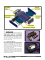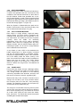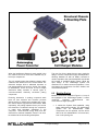
1
Table of Contents
Table of Contents .........................................................................................................................................1
List of Figures...............................................................................................................................................3
List of Tables................................................................................................................................................5
Abstract ........................................................................................................................................................6
1
Introduction ........................................................................................................................................8
1.1
Humanitarian Demining......................................................................................................................8
1.2
Chargers for Humanitarian Demining ..................................................................................................8
2
Problem Definition..............................................................................................................................9
2.1
Demining Industry Contacts ...............................................................................................................9
2.2
Design Requirements ........................................................................................................................9
2.3
Common Pitfalls .............................................................................................................................. 10
2.4
Working Conditions ......................................................................................................................... 10
3
Background on Battery Technology ................................................................................................. 11
3.1
The Alkaline Battery......................................................................................................................... 11
3.2
The Nickel-Cadmium Battery ............................................................................................................ 12
3.3
The Nickel-Metal-Hydride Battery ..................................................................................................... 14
3.4
End of Life in NiCd and NiMH........................................................................................................... 15
3.5
The Right Battery for the Job............................................................................................................ 16
3.6
Charging Nickel-Chemistry Batteries ................................................................................................. 16
3.7
Technically Speaking ....................................................................................................................... 18
4
Background on Solar Power............................................................................................................. 19
4.1
Solar Panels ................................................................................................................................... 19
4.2
Rigid Photovoltaic panels ................................................................................................................. 19
4.3
Semi Permanent Panels .................................................................................................................. 20
4.4
Foldable PV Panels ......................................................................................................................... 21
4.5
Disadvantages of Solar Power.......................................................................................................... 22
5
Alternatives to Solar Power.............................................................................................................. 23
5.1
Generators ...................................................................................................................................... 23
5.2
Vehicle Power ................................................................................................................................. 23
5.3
AC Mains ........................................................................................................................................ 24
5.4
Concluding Remarks on Power ........................................................................................................ 24
6
Current Battery Charging Technology.............................................................................................. 25
6.1
Personal Chargers........................................................................................................................... 25
6.2
Industrial Chargers .......................................................................................................................... 25
6.3
Humanitarian Demining Chargers ..................................................................................................... 26
6.4
Discussion of Shortcomings ............................................................................................................. 27
7
Design Overview............................................................................................................................... 28
7.1
General Description......................................................................................................................... 28
7.2
Design Overview ............................................................................................................................. 29
8
Conceptual Design ........................................................................................................................... 32
8.1
Open Construction........................................................................................................................... 32
8.2
Modular Design ............................................................................................................................... 33
8.3
Autoranging Power Converter .......................................................................................................... 34
9
Mechanical Design............................................................................................................................ 35
9.1
Structural Chassis ........................................................................................................................... 35
9.2
Heat Management Components ....................................................................................................... 37
9.3
Cell Charger Module ........................................................................................................................ 41
9.4
Power Rails and Contacts ................................................................................................................ 44
9.5
Mounting Plate ................................................................................................................................ 46
10
Electrical Design – Autoranging Power Converter............................................................................ 47
10.1 General Description......................................................................................................................... 47
10.2 Power Filtering & Conditioning.......................................................................................................... 49
10.3 Autoranging Switch.......................................................................................................................... 49
10.4 Low Voltage Converter .................................................................................................................... 51
Table of Contents
Page 1 of 104
10.5 High Voltage Power Converter ............................................................................................................ 55
10.6 Output Filtering & Protection ............................................................................................................ 57
10.7 APC Status LED Lights.................................................................................................................... 58
11
Electrical Design – Cell Charger ....................................................................................................... 59
11.1 General Description......................................................................................................................... 59
11.2 Input Power Filtering & Regulation .................................................................................................... 61
11.3 Embedded Microcontroller ............................................................................................................... 61
11.4 The Switching Regulator .................................................................................................................. 62
11.5 Voltage and Current Feedback ......................................................................................................... 63
11.6 Thermal Monitoring.......................................................................................................................... 64
11.7 Battery Conditioning ........................................................................................................................ 65
11.8 ICSPI Interface................................................................................................................................ 65
12
Electrical Design – Cell Charger Operating System.......................................................................... 67
12.1 General Description......................................................................................................................... 67
12.2 Battery Qualification......................................................................................................................... 67
12.3 Charging Algorithm .......................................................................................................................... 68
12.4 Battery Conditioning ........................................................................................................................ 70
12.5 Calibration ...................................................................................................................................... 70
12.6 Regulator Control ............................................................................................................................ 71
12.7 Safety Assurance............................................................................................................................ 71
13
Electromechanical Design ................................................................................................................ 73
13.1 Surface Mount Components............................................................................................................. 73
13.2 Components Bonded to Heat Sinks .................................................................................................. 73
13.3 High Current Loops ......................................................................................................................... 73
13.4 PCB Layout Drawings ...................................................................................................................... 74
14
Production ........................................................................................................................................ 75
14.1 Mechanical Components................................................................................................................... 75
14.2 Mechanical Components Bill of Materials .......................................................................................... 76
14.3 Cell Charger Module Bill of Materials ................................................................................................ 77
14.4 Autoranging Power Converter Bill of Materials ................................................................................... 78
14.5 Final Assembly................................................................................................................................ 79
14.6 Calculation of Per-Unit Cost ............................................................................................................. 81
15
Cost Savings Analysis...................................................................................................................... 82
15.1 Organization A ................................................................................................................................ 82
15.2 Organization B ................................................................................................................................ 85
15.3 Synthesis........................................................................................................................................ 88
16
Future Design Plans (Mechanical) .................................................................................................... 89
16.1 Evaluation of Chassis Design .......................................................................................................... 89
16.2 Battery Contacts and Mud ................................................................................................................ 89
16.3 Last Wrench to Throw ...................................................................................................................... 90
17
Future Design Plans (Electrical) ....................................................................................................... 91
17.1 900kHz Switching Regulators ........................................................................................................... 91
17.2 Greatly Reduced Size...................................................................................................................... 91
18
Conclusion ....................................................................................................................................... 92
19
Author Biographies .......................................................................................................................... 93
References.................................................................................................................................................. 94
Table of Contents
Page 2 of 104
List of Figures
Figure 1-1: A Deminer at Work [1]....................................................................................................................8
Figure 1-2: Landmine Affected Countries [2] .....................................................................................................8
Figure 3-1: Construction of an Alkaline Battery. [25]. ....................................................................................... 11
Figure 3-2: Alkaline Internal Resistance. [27]. ................................................................................................. 11
Figure 3-3: Alkaline Self-Discharge. [30]......................................................................................................... 12
Figure 3-4: Construction of a NiCd Battery. [31]. ............................................................................................. 12
Figure 3-5: NiCd Discharge Curve. [33]. ......................................................................................................... 12
Figure 3-6: NiCd Charging Curve. [35]............................................................................................................ 13
Figure 3-7: NiCd Self Discharge with Temp. [31]............................................................................................. 13
Figure 3-8: NiCd Capacity Loss with Age. [31]. ............................................................................................... 13
Figure 3-9: Construction of a NiMH Battery. [38]. ............................................................................................ 14
Figure 3-10: NiMH Discharge Curve. [40]. ...................................................................................................... 14
Figure 3-11: NiMH Charging Curve. [42]......................................................................................................... 14
Figure 3-12: NiMH Capacity Loss with Temp. and Charge Rate. [44]................................................................ 14
Figure 3-13: Charge vs. Voltage for NiCd / NiMH. [47]..................................................................................... 16
Figure 3-14: Charge –vs.- Temp For NiCd / NiMH. [47]................................................................................... 17
Figure 3-15: Combined NDV and DT Algorithms. [47]...................................................................................... 17
Figure 3-16: NDV / DT Algorithm Critical Points. [43]....................................................................................... 18
Figure 3-17: Cells Labeled as Batteries .......................................................................................................... 18
Figure 4-1: NCL Panels With Road Case. [55] ................................................................................................ 19
Figure 4-2: NCL Road Case Closed. [56]........................................................................................................ 19
Figure 4-3: BP Solar Shatterproof PV Panels. [60]. ......................................................................................... 20
Figure 4-4: Flexible PV Panel on Boat. [61]. ................................................................................................... 20
Figure 4-5: UniSolar Foldable PV Panel. [64] .................................................................................................. 21
Figure 4-6: NCL Solar Folding PV Panel. [After: 65]. ....................................................................................... 21
Figure 4-7: BP SX 60 Curves @ 1KW/m2. [67]. .............................................................................................. 22
Figure 5-1: Wall-Mounted Electronics in MGM Vehicles. [72]. .......................................................................... 23
Figure 6-1: Alltek AT-5798 (left) and Maha C-204F. [74, 75]. ........................................................................... 25
Figure 6-2: Cell-Con 18 Bay Smart Charger. [77]. ........................................................................................... 26
Figure 6-3: PowerStream 16 Bay 800 W SLA Charger. [78]. ................................................................................. 26
Figure 6-4: The Minelab F-Series Charger. [81]. ............................................................................................. 27
Figure 7-1: Isometric View of the Intellicharge Battery Charging System............................................................ 28
Figure 7-2: Exploded, Labeled View of Intellicharge System ............................................................................. 29
Figure 7-3: Power Distribution Topology .......................................................................................................... 29
Figure 7-4: Cell Charger Module in Use........................................................................................................... 29
Figure 7-5: Applying a Thermal Interface Pad .................................................................................................. 30
Figure 7-6: Washing a Thermal Interface Pad .................................................................................................. 30
Figure 7-7: Translation Lock Battery Holder ..................................................................................................... 30
Figure 7-8: Mounting Plate & Power Input Connector ...................................................................................... 30
Figure 7-9: Assembling the Power Rails ......................................................................................................... 31
Figure 7-10: Loading Cell Charger Modules Into Chassis.................................................................................... 31
Figure 7-11: Securing the External Heat Sinks ................................................................................................. 31
Figure 7-12: Cell Charger Visible Through Access Port ................................................................................... 31
Figure 9-1: Front View of Structural Chassis................................................................................................... 35
Figure 9-2: Rendering of Current Chassis Design ........................................................................................... 35
Figure 9-3: Rear View of Structural Chassis ................................................................................................... 35
Figure 9-4: Orientation of the Chassis ............................................................................................................ 36
Figure 9-5: Cut-Away View of Cell Charger..................................................................................................... 37
Figure 9-6: Securing the Heat Spreader ......................................................................................................... 37
Figure 9-7: Installing a Thermal Interface Pad................................................................................................. 37
Figure 9-8: View of APC Showing Heat Spreader............................................................................................ 38
Figure 9-10: External Heat Sink. Inset: Beveled Corner................................................................................... 38
Figure 9-11: System with Top Mounted Heat Sinks ......................................................................................... 39
Figure 9-12: Bottom Mounted Heat Sinks ....................................................................................................... 39
List of Figures
Page 3 of 104
Figure 9-13: Bottom Mounted Heat Sinks (top view) ........................................................................................ 40
Figure 9-14: Detail of Negative Battery Contact .............................................................................................. 41
Figure 9-15: Detail of Positive Battery Contact ................................................................................................ 41
Figure 9-16: A Low Cost Battery Holder ......................................................................................................... 42
Figure 9-17: Battery Holder in a Consumer Grade Fast-Charger ...................................................................... 42
Figure 9-18: Battery Holder in an Industrial Flashlight ...................................................................................... 42
Figure 9-19: The Intellicharge Battery Holder .................................................................................................. 43
Figure 9-20: Inserting a Battery (Stage 1) ....................................................................................................... 43
Figure 9-21: Inserting a Battery (Stage 2) ....................................................................................................... 43
Figure 9-22: Inserting a Battery (Stage 3) ....................................................................................................... 43
Figure 9-23: Machined Components of Cell Charger ....................................................................................... 44
Figure 9-24: Connec2it High Durability Spring Contact .................................................................................... 45
Figure 9-25: CCM Arrangement if Rails were Centered ................................................................................... 45
Figure 9-26: Chassis Inside Two Piece Mounting Plate ................................................................................... 46
Figure 10-1: Autoranging Power Converter PCB Before Potting ....................................................................... 47
Figure 10-2: Circuit Diagram of APC Divided into Regions ............................................................................... 48
Figure 10-3: Detail of Power Filtering Components ......................................................................................... 49
Figure 10-4: Schematic of Power Filtering Components .................................................................................. 49
Figure 10-5: Autoranging Switch Components ................................................................................................ 49
Figure 10-6: MC33161 Internal Configuration and Graph of Typical Voltage Response. [126]. ........................... 50
Figure 10-7: Schematic of Autoranging Circuitry ............................................................................................. 50
Figure 10-8: Detail of Low Voltage Converter.................................................................................................. 51
Figure 10-9: Bulk Capacitors in the Low Voltage Converter ............................................................................. 51
Figure 10-10: Schematic of PWM Controller. .................................................................................................. 52
Figure 10-11: Winding the LV Flyback By Hand .............................................................................................. 53
Figure 10-12: LV Converter Output Diode and Caps ....................................................................................... 53
Figure 10-13: Schematic of Output Voltage Regulator ..................................................................................... 54
Figure 10-14: LV Converter Primary Clamp. ................................................................................................... 55
Figure 10-15: Detail of High Voltage Converter ............................................................................................... 55
Figure 10-16: HV Converter Aux Winding PSU............................................................................................... 56
Figure 10-17 HV Converter RC Network ......................................................................................................... 57
Figure 11-1: Main Components of the Cell Charger......................................................................................... 59
Figure 11-2: Cell Charger Circuit Diagram Divided into Regions....................................................................... 60
Figure 11-3: Input Filter and Regulator Components ....................................................................................... 61
Figure 11-4: Schematic of Regulator Components .......................................................................................... 61
Figure 11-5: Detail of Embedded Microcontroller. ............................................................................................ 61
Figure 11-6: Switching Regulator (3 Amp Version) .......................................................................................... 62
Figure 11-7: Schematic of Switching Regulator ............................................................................................... 63
Figure 11-8: Schematic of VCF Block............................................................................................................. 64
Figure 11-9: Digital Temp Sensor Mounted in CCM ......................................................................................... 64
Figure 11-10: Detail of Battery Conditioning MOSFET..................................................................................... 65
Figure 11-11: Schematic of Battery Conditioning Components......................................................................... 65
Figure 13-1: PCB Layout for the APC............................................................................................................. 74
Figure 13-2: PCB Layout for Cell Charger ...................................................................................................... 74
Figure 14-1: Preliminary Impression of Molded Design (Isometric View) [164] ................................................... 75
Figure 14-2: Preliminary Impression of Molded Design (Bottom View) [164] ...................................................... 75
Figure 15-1: Political Map of Mozambique Region [165]. ................................................................................. 82
Figure 15-2: The Ebinger EBEX 421 GC Detector [3]. ..................................................................................... 82
Figure 15-3: Political Map of Cambodia Region [174]. .................................................................................... 85
Figure 15-4: The Minelab F4 Mine Detector [3]. .............................................................................................. 85
Figure 16-1: Proposed Fastener Modifications ................................................................................................ 89
Figure 16-2: Partial Cut-Away View of Battery Holder ...................................................................................... 90
Figure 16-3: Alternative Battery Contacts ....................................................................................................... 90
Page 4 of 104
List of Tables
Table 3-1: Comparison of NiCd and NiMH. ..................................................................................................... 16
Table 3-2: Suggested Calibration Data. [43].................................................................................................... 18
Table 4-1: Price Comparison of Rigid PV Panels. [After: 58]. ........................................................................... 20
Table 4-2: Shatterproof and Flexible PV Pricing. [After: 63].............................................................................. 21
Table 14-1: BOM for Mechanical Components of the Intellicharge System........................................................ 76
Table 14-2: BOM for Cell Charger Components .............................................................................................. 77
Table 14-3: BOM for the Autoranging Power Converter................................................................................... 78
Table 15-1: Average Recorded Air Temperatures in Mozambique [167]............................................................ 83
Table 15-2: Average Wind Speeds Recorded in Mozambique [168]. ................................................................ 83
Table 15-3: Average Insolation Recorded in Mozambique [169]. ...................................................................... 83
Table 15-4: Average Frequency of Near-Overcast Skies Recorded in Mozambique [170]. ................................. 83
Table 15-5: Average Air Temperature Recorded in Cambodia [175]. ................................................................ 86
Table 15-6: Average Wind Speeds Recorded in Cambodia [176]. .................................................................... 86
Table 15-7: Average Insolation Recorded in Cambodia [177]. .......................................................................... 86
Table 15-8: Average Frequency of Near-Overcast Skies Recorded in Cambodia [178]. ..................................... 86
List of Tables
Page 5 of 104
Abstract
This paper details the design and construction of a new type of battery charger optimized for use in humanitarian
demining. It is our objective to design a battery charging system that is not only feasible, but also marketable to
the humanitarian demining community. To succeed, the system must overcome the shortcomings in existing
battery chargers that have prevented their successful deployment.
We begin by detailing the conditions under which deminers work, including the climate, work patterns, and
treatment of equipment. We describe the techniques we used to collect information from demining organizations,
and highlight problems with existing demining equipment.
Background knowledge on rechargeable batteries and solar cells is necessary to fully understand the design
problem. We present a concise explanation of both of these technologies, correcting a number of common
misunderstandings. The limitations of currently available battery chargers are also examined.
The Intellicharge System offers a cost-saving alternative to the ongoing use of disposable batteries. After
providing an overview of the design, justification is given for our conceptual decisions. The mechanical and
electrical design details are then fully disclosed, including complete engineering drawings and circuit board
layouts. Every detail of the design is consistent with the original objectives of the project.
Following the discussion of the design, we explain how the System could be manufactured on a commercial
scale. Assembly procedures for major components are examined in detail. The quantity at which molding
structural components becomes more cost efficient than machining them is also calculated. A thorough analysis
of production costs is provided, along with a complete bill of materials and detailed final assembly procedures.
The ultimate goal of the Intellicharge System is to save money for humanitarian demining organizations. Two
cost-benefit analyses are presented, demonstrating the economic viability of the Intellicharge System in different
usage scenarios.
Brief Description of Design
The Intellicharge System is designed to meet the needs of most humanitarian demining organizations. It is
capable of quickly charging large numbers of batteries under difficult operating conditions. It can operate from
almost any source of power and automatically sets itself to the correct voltage range. Under typical operating
conditions, the current design will charge eight 4,000mAh D-size batteries in about an hour. The next revision of
the design will charge eight 8,000mAh D-size batteries in the same amount of time.
The System is designed to be shipped and stored without a transport case, and is built to withstand shock,
vibration, and repeated impacts. The System is completely waterproof, even when disassembled.
All of the components used in the Intellicharge System have been specifically chosen to resist the effects of oil,
dirt, sand, and abrasive grit. Since the System is convection-cooled, there are no fans or ventilation slots to get
plugged
The Intellicharge System is designed to be serviced in the field, and can be completely disassembled with only
two wrenches. Other than the six nuts that hold it together, there are no small parts to get lost or damaged. The
whole System is modular, so replacing parts is also greatly simplified
The Intellicharge System measures 29.6cm x 40.4cm x 8.8cm, and weighs about 7kg. It contains eight Cell
Charger Modules (CCM) and one Autoranging Power Converter (APC) Module. All nine modules slide into
spaces within a structural frame, called the Chassis. Two aluminum heat sinks bolted onto either side of the
Chassis hold the nine modules in place. The entire unit is fixed to a stainless steel plate with a sturdy handle. The
plate has holes punched through it to facilitate bolting or screwing onto any flat surface, horizontal or vertical.
Abstract
Page 6 of 104
Each Cell Charger Module is an independent battery charger. The user plugs a power source into the APC
Module, which then outputs a regulated supply of 12 volts DC to the eight CCM’s. Each of the eight chargers
operates independently. If one were damaged, the other modules would continue to function normally.
The current CCM design can test, charge, and monitor a single D-size battery. In the future, three more variations
of the CCM will be designed to charge a C-size, 9-volt, or two AA-size batteries. In the case of the AA-size
module, the two batteries will still be tested and monitored independently.
All Cell Charger Modules will be interchangeable so that the Intellicharge System can be used with any
combination of eight CCM’s, simultaneously charging D, C, 9-volt, and AA size batteries.
Major Achievements
To succeed at this project, we had to adapt solutions from a wide variety of unrelated industries. The Intellicharge
System has the following advantages over currently available battery chargers:
•
•
•
•
•
The Autoranging Power Converter which permits the use of virtually any power source, even those with
fluctuating and/or intermittent output
Independent, microprocessor-controlled battery chargers which:
o allow the charging of odd numbers of batteries, inserted at random and removed as required
o identify non-rechargeable batteries as well as damaged, open or shorted rechargeables
o prevents overcharging of batteries, even with mixed battery types and varied levels of discharge
o can condition nickel-cadmium batteries in a fraction of the time that other battery chargers require
o use simple LED indicators to clearly display the status of each battery
Translation-lock battery holders which make it virtually impossible for batteries to fall out of the charger,
allowing the device to be mounted vertically in a vehicle and operated while in motion
Potted, conduction-cooled electronics which make the Intellicharge System impervious to water while
facilitating rapid cooling
Modular construction which simplifies component replacement and allows customization of the System to
each users needs
While further testing and development is needed before field testing can begin, most of the major design
obstacles have already been overcome.
Abstract
Page 7 of 104
1 Introduction
1.1
Humanitarian Demining
Humanitarian demining is the tedious, precise, and
potentially dangerous job of removing anti-personnel
and anti-vehicle landmines from post-conflict areas.
1.2
Chargers for Humanitarian
Demining
As part of the process of getting the mines out of the
ground, almost every demining organization uses
portable metal detectors. Most of these detectors
are designed to run from standard “Consumer Size”
batteries, in particular, C-size and D-size batteries.
[3]. Each detector takes between 3 and 8 of these
batteries, and they can last anywhere from 2 to 5
days under heavy usage. [4].
It is not unusual for a single group of deminers to
have dozens of detectors in use at once. As a
consequence, many organizations go through
thousands of disposable batteries every month. For
many, the cost of batteries is a significant and
ongoing expense. [5, 6].
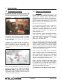
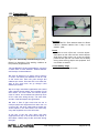
Figure 1-1: A Deminer at Work [1].
This process often involves the removal of rockets,
grenades, and other unexploded shells, in addition
to the landmines. Such devices are collectively
referred to as UXO.
Landmines are a global problem, and present in
countries spread across the entire planet. As a
result, humanitarian demining organizations work
under a diverse set of social, economic, and climatic
conditions.
Properly deployed, modern rechargeable batteries
could offer a significant cost savings to many
humanitarian demining organizations. Unfortunately,
there are several obstacles to successful
deployment of this technology.
First, the batteries used must have high enough
capacity to run the detectors for a reasonable length
of time. The batteries must also be able to withstand
vibration during transport and tolerate charging
under hot conditions. Most consumer grade batteries
cannot meet these demands. A complete discussion
of batteries is presented in Section 3.
Second, a low cost, reliable source of electrical
power is needed to serve as an energy source from
which to charge the batteries. Since deminers often
work in remote locations far away from conventional
wall outlets, finding a suitable source of power
becomes an interesting challenge. Power source
options are discussed in Sections 4 and 5.
Figure 1-2: Landmine Affected Countries [2]
Every demining organization is unique. They use
different equipment, different Standard Operating
Procedures (SOP’s), and often have different
overall goals. Any equipment marketed to these
organizations must be versatile enough to satisfy the
needs of many different groups.
Finally, a charger is needed that can quickly charge
large numbers AA, C, D-size, and 9-volt batteries.
The charger has to be reasonably priced, efficient,
waterproof, and highly durable. The design of such a
device forms the basis of this report.
The description of our design starts in Section 7.
Introduction
Page 8 of 104
2 Problem Definition
There are hundreds of different battery chargers on
the market today; hundreds that are not being used
in demining operations.
Humanitarian Demining. This input also helped our
design process.
Our design had to be an exception. To develop a
marketable device, we asked demining operators
what it was they wanted.
There are five design criteria that we see as
absolutely essential to the marketability of the
Intellicharge Battery Charging System. Each was
mentioned by the contest judges and repeated by
the many other people we talked to. The device
must:
2.1
Demining Industry Contacts
Only with relentless determination were we able to
contact deminers and demining operators from all
over the world. On their responses we based our
perception of the design problem.
With the information gathered, a list of key design
requirements was compiled. We also gained some
important insights into the day-to-day operations of
humanitarian demining operations, and into the
failures of existing technology to meet their needs.
For determining the needs of end-users, our primary
source of information was the MgM Forum. The
forum is a mailing list facilitated by Stiftung
Menschen gegen Minen (The Humanitarian
Foundation of People Against Landmines). By
posting questions, as well as a survey, to the forum
we initiated our correspondence with 12 different
individuals of various backgrounds.[7-17]
Valuable input was also received from the judges of
the Mines Action Canada Technology Research
Competition. In addition to answering our specific
questions, key requirements for a successful battery
charger were highlighted in their comments on past
submissions to the competition. [18,19].
A few people with extensive demining experience
were also found within Canada. Bill McAuley and
Steve
Stamp
both
served
as
Canadian
peacekeepers in Bosnia. The two enabled us to put
our research into context by enlightening us to
common demining procedures and aspects of the
humanitarian demining industry as a whole. [20,21]
We also interviewed two Kosovar women. They
were traveling across the Canada to speak about
their experiences working as deminers with
Norwegian People’s Aid. [22]
Once we had a general idea of where we wanted to
take our design, we called up several companies
that manufacture demining equipment and
discussed their experiences designing equipment for
2.2
•
•
•
•
•
Design Requirements
Indicate each battery’s charge state in a
reliable and unambiguous manner.
Charge batteries quickly enough to keep up
with the rapid rate at which demining
operations deplete them.
Be fully functional at the extreme temperatures
and humidity levels.
Be able to run off of vehicle batteries,
generators, solar panels and AC mains.
Be of sufficient physical durability to withstand
the rough, heavy usage prevalent in demining
operations.
Despite the numerous differences between one
demining operation and the next, there was a
surprising degree of consistency in the responses
we received. Expanding on the five critical
requirements listed above, it was generally agreed
that the battery charger should:
•
•
•
•
•
•
•
•
•
•
•
•
Be highly reliable.
Withstand exposure to dust, humidity, mud,
rain, and sand.
Adapt to various battery sizes and chemistries.
Require minimal operator training.
Automatically reject damaged and/or nonrechargeable batteries.
Charge a set of batteries in four hours or less.
Offer the user the choice of mounting it on a
flat surface that is either horizontal or vertical.
Be capable of operating while mounted in a
vehicle.
Be capable of operating from “dirty” and/or
intermittent power sources.
Have a minimal number of switches, buttons,
and indicator lights.
Be possible to disassemble and reassemble
with common tools.
Have a reasonable price tag.
The Intellicharge Battery Charging System meets
every one of the requirements listed above.
Problem Definition
Page 9 of 104
2.3
Common Pitfalls
Beyond the main design requirements, there are
other factors that must be considered when
designing equipment that is intended to be used in
the field:
•
•
•
•
•
Small parts are easily lost.
Parts can become contaminated with mud,
grit, and dirt.
Electrical connectors are usually small and
difficult to work with.
Threads can get stripped and/or eroded by
sand, damaging the device.
Seals fail, resulting in damage due to rain or
humidity.
Numerous steps were taken to mitigate the problems
above: The components of the Intellicharge System
are large and durable so that they are easy to
handle. The electronics inside the Intellicharge
System are encased in thermally conductive potting.
There are no seals in the design. All components
are waterproof and easy to clean.
and bolts are far less expensive to replace than an
entire battery charger.
2.4
Through our interviews and email correspondence,
important points were raised that helped us
understand the design problem at hand. [16]. Each
of the following generalizations were made by at
least three different people working in the
humanitarian demining industry.
At most demining operations:
•
•
•
•
•
•
•
•
screw
bolt
•
nut
•
Figure 2-1: Clarification of Screws and Bolts
Threaded fasteners could not be avoided entirely
and the system does contain six, standard sized
nuts. Nuts and bolts were used instead of screws
because, when the threads wear out, both parts of
the fastener can be replaced.
Working Conditions
•
•
Multiple sources of power such as generators,
vehicles, and AC mains are available.
When used, generators are typically run for
four hours each day, usually in the evening.
Power sources are not reliable. Generators
break down and AC mains switch off without
notice.
Banks of vehicle batteries are often used as
back-up power supplies.
Deminers start work early so that they can
avoid the mid-day heat.
Mine detectors are left on continuously
throughout the working day.
Equipment is frequently handled roughly
and/or abused.
Equipment is taken apart and cleaned, or
otherwise maintained, on a weekly basis. At
least a minimal level of maintenance is done
every day.
Operators are accustomed to fixing things
themselves. It can be assumed that at least
some people within the organization have
mechanical expertise.
Organizations usually own more than one type
of mine detector. Different types of mine
detectors often require different sizes of
batteries.
It is usually slow and very expensive to ship in
replacement parts for equipment.
Operators are willing to pay more money for
equipment that offers higher performance and
greater reliability.
The difference between bolts and screws is
sometimes misunderstood. To clarify: bolts are used
with nuts; screws are inserted into a threaded hole
on the device itself (Figure 2-1).
Threads will erode; it is only a matter of time. If
screws were used there would have to be threads
on the battery charging device itself. Damaged nuts
Problem Definition
Page 10 of 104
3 Background on Battery Technology
The most expensive component of any large scale
recharging operation is the batteries, not the charger.
[23].
1
Proper selection of batteries for a given application
is crucial to the success of the project. The decision
to use a given chemistry of battery must be made on
a case-by-case basis taking the full scope of the
organization into account. Different equipment,
different operating conditions, and different user
expectations make some batteries better suited than
others for a given set of working conditions and
usage patterns.
3.1
The Alkaline Battery
Disposable alkaline batteries are the battery of
choice for many demining organizations thanks to
their low cost, high capacity, and long shelf life.
There are at least six different chemistries of
rechargeable
batteries
widely
available
to
consumers:
•
•
•
•
•
•
Rechargeable Alkaline [RAM]
Nickel-cadmium [NiCd]
Nickel-metal-hydride [NiMH]
Lead-acid [PbSO4]
Lithium-ion [LiI]
Lithium-polymer [LiP]
Unless an organization is willing to build custom
battery adapters, modify circuitry, or fabricate
external battery packs, battery selection is greatly
simplified:
To work in a device that is designed to run off of
typical, consumer-sizes of batteries, the battery has
to have a terminal voltage of 1.2 to 1.65 volts, and it
has to meet ANSI dimensional standards.
There are only three battery chemistries that meet
both of these requirements: Nickel-cadmium, Nickelmetal-hydride, and Rechargeable Alkaline.
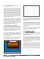
Figure 3-1: Construction of an Alkaline Battery. [25].
A typical D-size battery has a capacity of 18,000mAH
and costs around $1.50 USD when purchased in
quantity [26]. A cylindrical-construction alkaline
consists of a steel can containing a powdered zinc
anode and a manganese dioxide based cathode.
The two electrodes are separated by a thin layer of
non-woven fabric which is saturated with a
potassium hydroxide based electrolyte. Connection
to the powdered zinc anode is made with a brass
current collector pin.
While
Rechargeable
Alkaline
batteries
are
inexpensive and widely available, they also have two
serious drawbacks: a complete charge cycle takes at
least 16 hours, and, each battery can only be
recharged about 20 times (with a considerable
decrease in capacity each time). [24].
Because of their long recharge time and short
service life, rechargeable alkalines are not suitable
for use in humanitarian demining operations. Their
usage will not be discussed further.
1
A “battery” and a “cell” are not, technically, the same
thing. Please refer to Section 3.6.
Figure 3-2: Alkaline Internal Resistance. [27].
Background on Battery Technology
Page 11 of 104
This construction gives the battery a high internal
resistance, typically starting at around 150 milliohms
and progressively increasing over the service life of
the battery. The internal resistance varies with
temperature, and also the rate at which the battery is
being discharged.
The internal resistance of the battery has a
significant impact on its performance. While a typical
D-size alkaline technically has a capacity of
18,000mAH, a large portion of this capacity can only
be used if the battery is discharged very slowly. [28].
With modern electronic devices, this is rarely the
case.
applications, they still represent the best choice for
many users.
3.2
The Nickel-Cadmium Battery
The nickel-cadmium battery, or “NiCd”, has a
completely different construction from alkalinechemistry batteries and very different electrical
characteristics.
Many electronic devices, such as handheld two-way
radios and certain metal detectors, place a
significant load on the battery. In these applications,
alkalines may only last 30% longer than a typical
NiMH battery.
When powering loads with extremely high current
draw, the internal resistance of an alkaline battery
causes a large portion of the battery’s stored energy
to be dissipated as heat. As a result, alkaline
batteries can actually have a shorter service life than
comparable NiCd or NiMH rechargeables. A good
example of this is powering a camera flash. In this
application, NiMH batteries typically last 40% longer
than alkalines. [29].
Figure 3-4: Construction of a NiCd Battery. [31].
A typical D-size NiCd battery has a capacity of
4,400mAH and costs roughly $9.00USD when
purchased in quantity. [32]. Under perfect
conditions, it can be recharged thousands of times.
The cylindrical-construction NiCd consists of a
stainless steel can containing a positive plate, which
uses nickel hydroxide as its active material, and a
negative plate which uses a cadmium compound. A
separator made of a thin non-woven fabric is placed
between the plates and is saturated with an alkaline
electrolyte, typically potassium hydroxide.
A safety valve is used to vent the battery if the
internal pressure becomes dangerously high. The
valve is integrated into the top of the can beneath
the positive terminal.
Figure 3-3: Alkaline Self-Discharge. [30].
One benefit of alkaline batteries is that they have a
very low rate of self-discharge. Most alkaline
batteries can be stored for years without losing a
significant portion of their energy, even at elevated
temperatures. This makes alkaline batteries well
suited for standby applications, where the batteries
and the device they power are stored for long
periods of time between uses.
While alkaline batteries cannot be recharged and
are not suitable for extremely high current
Figure 3-5: NiCd Discharge Curve. [33].
Background on Battery Technology
Page 12 of 104
NiCd batteries have several electrochemical
characteristics that differentiate them from other
chemistries. First, NiCd batteries have very low
internal resistance, allowing the battery to be
charged or discharged very quickly and to hold its
terminal voltage constant over most of the battery
life.
Second, NiCd batteries exhibit a drop in terminal
voltage and an increase in temperature when the
battery reaches capacity during charging. This
phenomenon is most noticeable when the batteries
are charged at a rate greater than 0.5C (i.e.: half the
capacity of the battery per hour). [34].
Fourth, NiCd batteries have an exceptionally long
cycle life when properly maintained. Most
manufacturers rate their NiCd batteries for 1,000
charge/discharge cycles, but substantially longer
lives can often be achieved. [36].
The capacity of a properly maintained NiCd drops
slowly over the course of its service life, reaching
about 83% after 500 cycles.
Figure 3-8: NiCd Capacity Loss with Age. [31].
Figure 3-6: NiCd Charging Curve. [35].
Third, NiCd batteries have a high rate of selfdischarge, and it increases with the temperature at
which they are stored. A typical NiCd will retain 80%
of its energy after 2 months in storage at 20°C. If the
temperature is increased to 45°C, the energy
retained drops to just 20%. [31].
Because of this high self-discharge rate, NiCd
batteries are best suited for applications where they
can be used soon after charging, rather than being
left in storage for long periods of time.
Some D-Size NiCd’s can be fast-charged, others
cannot.
NiCd batteries exhibit a behavior called voltage
depression, also known as the “memory effect”.
If repeatedly recharged after being only partially
discharged, a NiCd will begin to grow metallic crystal
formations between its plates. These eventually start
to act as microscopic short circuits between the
plates, resulting in decreased capacity. This
phenomenon is commonly referred to as the
“memory effect.”
In order to counter the memory effect, NiCd batteries
occasionally have to be “exercised.” That is, they
must be completely discharged and then fully
recharged. This causes the crystal formations to
dissolve into the electrolyte. Since the charge
process is much faster than the rate of crystal
growth, it takes many partial charge-discharge
cycles for the crystals to re-form.
NiCd batteries should be exercised, at most, once
every 30 uses. More frequent cycling reduces the
service life of the battery. [37].
Figure 3-7: NiCd Self Discharge with Temp. [31].
Background on Battery Technology
Page 13 of 104
3.3
The Nickel-Metal-Hydride Battery
The nickel-metal-hydride battery, or “NiMH”, uses a
similar construction to NiCd based batteries with
different electrochemical ingredients.
NiMH batteries have very low internal resistance,
allowing them to be charged and discharged very
quickly. As with a NiCd, the NiMH holds its terminal
voltage constant over almost its entire charge life.
During charging, the terminal voltage drops and the
battery temperature increases rapidly when the
NiMH battery reaches capacity. However, at
elevated temperatures the magnitude of the voltage
drop is far lower than that of a NiCd. With charge
rates lower than 0.5C, it is almost nonexistent. [41].
Figure 3-9: Construction of a NiMH Battery. [38].
A cylindrical-construction NiMH consists of a
stainless steel can containing a positive plate, which
uses nickel hydroxide as its active material, and a
special hydrogen-absorbing alloy for the negative
electrode. A separator made of a thin non-woven
fabric is placed between the plates and is saturated
with an alkaline electrolyte consisting mainly of
potassium hydroxide.
A safety valve is integrated into the top of the can to
vent the battery if the internal pressure becomes
dangerously high.
Figure 3-11: NiMH Charging Curve. [42].
In addition, the charging process for a NiMH battery
becomes very inefficient for low charge rates as the
temperature of the battery is increased. A typical
NiMH will charge to full capacity with a 0.1C charge
rate at 20°C. If the temperature is increased to 45°C,
the capacity ratio drops to just 65%. If the charge
rate is now increased to 1.0C, the capacity ratio
increases to 96%. [43].
NiMH batteries offer 30-40% higher capacity than
comparable sized NiCd's, but at the expense of
durability and cycle life. [39].
Figure 3-12: NiMH Capacity Loss with Temp. and
Charge Rate. [44].
Figure 3-10: NiMH Discharge Curve. [40].
Many of the electrical characteristics of NiMH
batteries are similar to those of NiCd's.
Due to the voltage drop and capacity ratio effects,
NiMH batteries usually cannot be slow-charged. If
slow-charging is attempted, there is a serious risk of
overcharging the battery. A NiMH battery is quickly
Background on Battery Technology
Page 14 of 104
and severely damaged by overcharge, resulting in a
permanent loss of capacity. [46].
Self-discharge in most NiMH batteries is comparable
to that of NiCd's. A typical NiMH loses about 3% of
its energy per day when stored at 45°C. [45].
NiMH batteries are especially difficult to charge
properly at high temperatures, and usually cannot be
charged at temperatures higher than 45°C.
reaches a safe level. The loss of electrolyte causes
significant loss of capacity. The problem is
compounded if the safety vent does not re-seal
correctly and continues to leak electrolyte.
When a battery can only hold 70% of its rated
capacity, it is usually considered defective, and
should be replaced.
NiMH batteries exhibit a memory effect similar to
that experienced with NiCd batteries. While it is less
pronounced than with NiCd's, NiMH batteries should
occasionally be put through a complete chargedischarge cycle as a preventative measure. [46].
3.4.2 HIGH RATE OF SELF DISCHARGE
In batteries that have been damaged or are
approaching the end of their service life, the
insulator separating the electrodes can begin to
break down, causing short circuits between the
electrodes. This should not be confused with the
previously explained “memory effect”.
One of the major strikes against NiMH batteries is
their short cycle life. The performance of a typical
NiMH battery begins to fall off quickly after 300
cycles, and is made even worse by high operating
temperatures. [47].
The short circuits greatly increase the self-discharge
rate of the battery, causing it to quickly lose any
stored energy. This condition cannot be corrected,
and batteries showing this behavior should be
replaced.
The short cycle life combined with the marginal
(30%) increase in capacity and significant increase
in cost means that for a given investment in
batteries, NiMH batteries will deliver a far lower total
amount of energy over their lives than comparable
batteries, such as NiCd's. This is reflected in the
much higher Cost Per Cycle figure listed in
Table 3-1.
3.4.3 INTERNAL SHORT
A short circuit between the electrodes of a NiCd or
NiMH battery is an end-of-life failure. It occurs in
batteries with manufacturing defects or batteries at
the end of their service life.
3.4
End of Life in NiCd and NiMH
Even with proper maintenance, NiCd and NiMH
batteries will eventually wear out. It is also possible
for batteries to be damaged by misuse.
Worn-out or damaged batteries usually show four
distinct modes of failure:
•
•
•
•
Significantly Reduced Capacity
High Rate of Self-Discharge
Internal Short
Open Circuit
3.4.1 SIGNIFICANTLY REDUCED CAPACITY
With continued use, the capacity of a NiCd or NiMH
battery will slowly decrease over time. This results in
shorter run times for equipment powered by the
battery.
While it is often possible to melt or “zap” an internal
short by applying a high amperage current pulse to
the battery, doing so causes serious damage to the
battery. Batteries “repaired” in this manner will not
function reliably and should not be used.
3.4.4 OPEN CIRCUIT
An open circuit between the electrodes of a NiCd or
NiMH battery is also an end-of-life (EOL) failure. It
occurs in batteries with manufacturing defects, or
batteries that have been damaged by misuse.
This condition is usually caused by failure of one of
the connecting strips between the battery electrodes
and the external terminals. This can happen by
physical impact, or by the connecting strip melting
from excessive current draw. An open-circuit failure
can also occur if the battery has lost almost all of its
electrolyte.
These conditions cannot be corrected, and batteries
showing this behavior should be replaced.
If a NiCd or NiMH battery is overcharged, or
discharged at an extremely high rate, the heat
generated may boil the electrolyte. This causes the
battery to vent electrolyte until the internal pressure
Background on Battery Technology
Page 15 of 104
3.5
factor. These users will probably want to use NiMH
Batteries.
The Right Battery for the Job
All of the previously discussed batteries have unique
advantages and disadvantages that make them the
best candidate for a given application.
The Intellicharge System includes automatic battery
exercising hardware, and is capable of operating at
a sustained high temperature, simplifying the use of
NiCd’s and allowing charging of high-temperature
NiCd’s at high operating temperatures.
For operations that use their equipment lightly with
long periods of storage in between, nonrechargeable alkalines are probably the best choice.
The cost of buying and managing a rechargeable
battery system it is difficult to justify for such a light
use application.
We recommend the use of NiCd batteries over NiMH
batteries for almost all applications. Despite the
reduced capacity and the possible disposal
problems that come with these batteries, they are
the clear winner in terms of durability, reliability,
service life, and cost
For users with more demanding requirements, the
choice lies between nickel-cadmium and nickelmetal-hydride batteries.
A comparison of battery characteristics is listed in
Table 3.1.
As can be seen in table 3-1, NiMH batteries have
the highest capacity, and require exercising less
frequently than NiCd's. They also have the highest
initial cost, and lowest cycle life, resulting in the
highest cost per cycle.
3.6
Because NiCd and NiMH batteries have similar
charge-discharge behavior, both types of batteries
can be charged using the same electronics. Trickle
charge rate aside, a well designed charger doesn’t
have to be able to tell NiCd and NiMH batteries
apart, it just has to be able to tell when both types of
batteries have reached capacity.
NiCd batteries have a lower capacity than NiMH's,
but also a much lower initial cost and much longer
cycle life, resulting in the lowest cost per cycle. They
do, however, need to be exercised more frequently
than NiMH batteries.
Table 3-1: Comparison of NiCd and NiMH.
Gravimetric Energy
Density (Wh/kg)
NiCd
NiMH
45-80
60-120
Cycle Life (to 75% of initial 1500
capacity)
As mentioned earlier, both NiCd and NiMH batteries
exhibit an increase in terminal voltage as the battery
is charged, and a decrease or plateau in terminal
voltage once the battery has reached capacity
(exceeded, actually). A charger can use this
phenomenon to tell when the battery is full, and to
stop the charge cycle. This technique is called
Negative Differential Voltage (NDV). [48].
300 to
500
Fast Charge Time
1h typical 1h +
Overcharge Tolerance
moderate low
Self-discharge / Month
(room temperature)
20%
Vibration Resistance
Moderate Low
Charging Temperature
Up
60°C
Maintenance Requirement
30
to 60
60 days 90 days
Typical Battery Cost
(US$, reference only)
$10.00
$17.00
(1.5V, D) (1.5V, D)
Cost per Cycle (US$)
$0.009
Charging Nickel-Chemistry
Batteries
30%
to Up to
45°C
to
$0.04
Figure 3-13: Charge vs. Voltage for NiCd / NiMH. [47].
For some users, having the longest run time
electrochemically possible is the greatest motivating
Unfortunately, there is a minor problem. NiMH
batteries have a much lower voltage drop than
Background on Battery Technology
Page 16 of 104
NiCd’s, and at charging temperatures over 45°C it
might not even be measurable. Accordingly, a
charger using this phenomenon alone could miss
the voltage drop and overcharge the battery.
Another characteristic of both NiCd and NiMH
batteries is that the temperature of the battery
increases rapidly as the battery approaches
capacity. More specifically, the rate of change of
temperature increases.
By measuring the temperature of the battery when it
is first placed in the charger, subtracting it from the
temperature measured during the charge process,
and comparing the rate of increase of the
temperature readings, a charger can use this
second phenomenon to tell when the battery is full
and to stop the charge cycle. This technique is
called Differential Temperature (DT). [48].
Figure 3-15: Combined NDV and DT Algorithms. [47].
By combining both NDV and DT techniques, its
possible to end the charge cycle for both NiCd and
NiMH batteries at the right time with a high degree of
accuracy. [52].
A charger using this algorithm simultaneously
monitors the temperature and terminal voltage of the
battery under charge. The NDV trigger threshold is
set to a very low value, allowing the weak response
of a NiMH battery to be detected. When the
controller
detects
a
temperature
rise
in
synchronization with a drop or plateau in terminal
voltage, it ends the charge cycle. [47].
Figure 3-14: Charge –vs.- Temp For NiCd / NiMH. [47].
Unfortunately, there are several possible problems
with this technique as well. First, a NiMH battery
gets much hotter much faster than a NiCd. A charger
using this technique alone could prematurely end
the charge cycle on NiMH batteries.
Second, if the charger is left outside on a cloudy day
and the sun comes out, the temperature increase
could also end the charge cycle ahead of schedule.
Because both measurements are used as part of the
decision process, false triggering by sunlight or
noise in the voltage measurement circuitry is
avoided. The algorithm can be expanded to take
ambient temperature, elapsed time, and expected
battery capacity into account.
At the very least, the device should have a safety
timer that terminates the charge cycle after a certain
maximum time period has elapsed.
Figure [3-16] and Table [3-2] show this algorithm
optimized for the Panasonic brand (both NiCd and
NiMH) rechargeable batteries.
Clearly, neither of these techniques alone will
provide satisfactory results when charging both
NiMH and NiCd batteries outdoors using the same
charger.
Background on Battery Technology
Page 17 of 104
Table 3-2: Suggested Calibration Data. [43].
3.7
Technically Speaking
To be technically accurate, there is a difference
between a cell and a battery.
A cell is a single electrochemical assembly with one
anode and one cathode that generates a voltage
dependant on the electrochemical system it uses.
Figure 3-17: Cells Labeled as Batteries
A Battery consists of two or more cells connected
together to increase the voltage or current capacity
of the assembly. Therefore, a 1.5 volt D-size
“battery” is actually a cell, while a 9 volt “battery”
(containing six 1.5V cells wired in series) truly is a
battery.
Figure 3-16: NDV / DT Algorithm Critical Points. [43].
It seems that most, if not all, manufacturers label
their products as batteries regardless of what is
actually inside them.
Throughout this report, we will refer to D, C, and AAcells as batteries, adopting the naming system used
by the manufacturers.
Background on Battery Technology
Page 18 of 104
4 Background on Solar Power
One major obstacle to the widespread deployment
of rechargeable batteries in humanitarian demining
is finding a reliable power source from which to
charge them. More often than not, deminers have to
work in rural or underdeveloped areas, far from an
AC wall outlet
To function in the demining environment, a battery
charger has to be able to work with unconventional
sources of power, and to overcome the unique
challenges that they represent. This section of the
report explores the power sources available at a
typical demining operation, and examines the
specific challenges involved in using each source.
4.1
Solar Panels
Past entries have categorized solar panels based on
their molecular structure, differentiating between
monocrystalline, multicrystalline, and amorphous
cells. With advances in technology, classification is
no longer so simple.
Manufacturers now use all sorts of proprietary
technology to enhance their products. [49,50]. One
large manufacturer layers three thin-film narrow
band amorphous solar cells on top of each other to
produce power densities approaching that of a
polycrystalline cell. [51]. Another large manufacturer
uses a proprietary Edge-defined film fed growth
process to significantly enhance the power output of
their polycrystalline cells. [52].
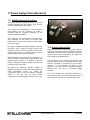
Figure 4-1: NCL Panels With Road Case. [55]
A more realistic way to list solar panels is based on
their intended use: Fixed installation, semi
permanent, and foldable.
4.2
Rigid Photovoltaic panels
Figure 4-2: NCL Road Case Closed. [56].
The absolute highest power output per dollar ratio
comes from rigid PV (photovoltaic) panels. [53].
A rigid PV panel is intended for permanent
installation, either on the roof of a building or bolted
to some kind of support structure. Most of these
panels are surprisingly durable, rated to survive
200km/h winds and 25mm hailstones impacting at
terminal velocity. [54].
For maximum efficiency, rigid PV panels usually
have tempered glass fronts. The glass front will
crack if the panel is dropped on a hard surface.
By adding a road case that doubles as a support
frame, a rigid PV panel can be used as a portable
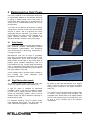
energy source, as shown in this system from NCL
Solar. [57].
The durable road case allows glass-fronted panels
to survive normal transport and handling. The
integrated frame allows them to be angled towards
the sun, and prevents them from being blown over
by wind. In many countries, this is an important
consideration.
Background on Solar Power
Page 19 of 104
Below is a list of typical market prices for rigid PV panels (as of Apr 17, 2002) ranked by dollars per watt:
Table 4-1: Price Comparison of Rigid PV Panels. [After: 58].
Supplier
Solatron Technologies
Cheapest Solar
Alternative Energy Store
Advance Power Co
Alternative Energy Store
Solatron Technologies
Solatron Technologies
Alternative Energy Store
Advance Power Co
Sun Electronics
4.3
Brand Name
Photowatt
Siemens
Matrix
Siemens
Matrix
Photowatt
Photowatt
Matrix
BP Solar
Kyocera
Semi Permanent Panels
The next best power output per dollar ratio comes
from shatterproof PV panels. This class of panels is
more durable than rigid PV. They’re designed to be
moved from one location to another, or even
mounted on moving platforms such as boats and
RV’s (campers). These panels fall into two
categories, rigid PV with a shatterproof front and
thin-film flexible panels.
Watts
100
90
80
90
75
95
90
105
120
80
Min Qty
2
1
2
2
2
2
2
2
2
4
US$/Panel
$399.00
$360.00
$320.00
$360.00
$302.50
$389.00
$369.00
$434.50
$500.00
Call
US$/Watt
3.99
4.00
4.00
4.00
4.03
4.09
4.10
4.14
4.17
4.30
The high durability comes at the price of higher cost,
reduced output, and shorter service life due to
weathering of the plastic glazing film.
Shatterproof front panels, such as the units below
manufactured by BP Solar, are highly durable. They
can take repeated impacts without cracking. [59].
Their plastic fronts will “frost” if the panel is
constantly abraded against other equipment.
Figure 4-4: Flexible PV Panel on Boat. [61].
Flexible solar panels use thin-film amorphous solar
cells layered atop one another to generate
electricity. These panels can have surprisingly high
power output because each layer of cells is “tuned”
to absorb light of a different wavelength. By bonding
the cells to a thin sheet of stainless steel and
covering them with a flexible polymer, its possible to
make a somewhat flexible solar panel. [49, 50, 62].
These panels cannot be rolled up like a rug or folded
like a piece of paper, but they will bend to fit a
curved surface, like the roof of a bus.
Figure 4-3: BP Solar Shatterproof PV Panels. [60].
Because the panels have few rigid parts, and
contain almost no oxidizable metals, they are highly
resistant to corrosion and vibration. They can still be
damaged if driven over by a vehicle or repeatedly
stepped on.
Background on Solar Power
Page 20 of 104
In general, flexible solar panels are more expensive
and have significantly lower power output than either
shatterproof or glass fronted rigid PV modules.
Current (as of May 5, 2002) retail prices for
shatterproof, flexible PV panels are listed in the table
below.
Table 4-2: Shatterproof and Flexible PV Pricing. [After:
63].
PHOTOVOLTAIC PANELS
Price
Shipping
PVUS5
Unisolar 5 watt PV panel
65.00
9.00
PVUS11
Unisolar 11 watt PV panel
124.00
9.00
PVUS21
Unisolar 21 watt PV panel
149.00
12.00
PVUS32
Unisolar 32 watt PV panel
198.00
14.00
PVUS42
Unisolar 42 watt PV panel
245.00
16.00
PVUS64
Unisolar 64 watt PV panel
364.00
22.00
PVUSF5
Unisolar 5 watt flexible PV panel
89.00
9.00
PVUSF11 Unisolar 11 watt flexible PV panel 145.00
9.00
PVUSF32 Unisolar 32 watt flexible PV panel 289.00
14.00
4.4
Foldable PV Panels
Some applications require a solar panel that can be
quickly folded up and stowed away, then quickly
redeployed at another location. The panels in this
category are designed for military and high-end
consumer applications where cost is a secondary
concern.
Figure 4-6: NCL Solar Folding PV Panel. [After: 65].
One such system, manufactured by NCL Solar,
produces a peak power output of 10.8 watts.
List Price: $650.00 USD.
Another larger System, made by Uni-Solar,
produces a peak power output of 30 watts.
List Price: $780.00 USD.
Unfortunately, neither of these systems are well
suited for powering solar battery chargers. Their
high cost and low output are not justified by the
increase in portability that a folding system offers.
Because these panels are mounted on either a
plastic or fabric substrate, they are far less durable
than a shatterproof PV panel, and much less
resistant to weathering. While it is true that, as
advertised, either of the foldable panels could still
work after being riddled with bullet holes, they would
only continue to do so for a limited time. Following a
puncture, the expensive flexible PV cells would
quickly be destroyed by reaction with water from rain
and moisture in the air.
In most locations, a foldable PV panel would have to
be draped over some kind of rigid support so it could
be pointed at the sun. Since the support (e.g.: a
wooden board) would have to be transported along
with the panel, it would completely defeat the
purpose of making the panel foldable in the first
place.
In the context of powering an affordable and reliable
battery charger, foldable PV panels are a terrific
example of something that looks great on paper, but
is just not practical in the field.
Figure 4-5: UniSolar Foldable PV Panel. [64]
Background on Solar Power
Page 21 of 104
4.5
Disadvantages of Solar Power
Just because solar panels are reliable, low
maintenance energy conversion devices, does not
mean that they are reliable sources of power.
For a solar panel to work properly, it must be
correctly sized for the intended load and receive
large amounts of high intensity sunlight. This may
not be a problem in countries such as Sudan, but it
can be a major challenge in other mine-affected
countries.
Under these conditions, a typical rigid PV Panel,
such as the BP Solar BP-S X-60 pictured above, will
only generate about half the power output it is rated
for.
Assuming that 30% of the daily insolation happens
during the early morning and late evening, when the
light intensity is too low to get any power out of the
panel. And assuming that the remainder of the day,
the panel runs at its rated 11.5% efficiency [67], and
has 0.516m2 area, we get:
(1 – 0.3) x 4500 x 0.116 x 0.5160 = 188.4 Wh/Day
For example, consider an operation such as the
Cambodian Mine Action Center, mentioned in the
Mines Action Canada 2000 Technology Competition
Judges’ comments. Based on the detectors they
have in use, this operation would need 108
4,400mAH batteries charged per day. [19].
108 x 1.3 x 4.44 x 2 = 1,264.77
It will take over 1,200 watt-hours of energy per day
to charge those batteries, assuming the charger and
charging process runs at 50% efficiency.
Using satellite data from NASA and a very rough
calculation, we can say that the average daily
insolation in Cambodia is about 4.5kW/m2, with a
peak insolation of about 700W/m2. [66].
That’s 188.4 Watt-hours per 60-watt panel per day.
To get 1,200 WH/day will require seven panels.
Then there is the possibility that it could be raining or
overcast for a few days in a row. In order to still be
able to charge batteries, electrical power from the
solar panels will have to be stored using a bank of
lead-acid batteries. Assume we want to have 3 days
of electricity storage:
3 x 1,264 = 3,792 WH storage
3,792 / 12 = 316 AH battery capacity
316 Amp-Hours of battery capacity at 12 volts. That
is the equivalent of six, 55 amp-hour, 12 volt storage
batteries. Assuming that the charging process is
75% efficient, and that we want our battery bank to
be able to charge up in four days while still charging
the metal detector batteries, we need:
3,792 / (0.75 x 188.4 x 4) = 6.72 = 7
Seven additional solar panels added to the system,
bringing the total to fourteen panels.
(14 x 270) + (6 x 171) + (149) = $4,955.00
The completed solar array, including the charge
controller, will cost over $4,955.00 USD, measure
almost (3m x 3m), (10ft. x 10ft.), and including the
batteries, weigh over 762lbs (346kg).
Compared to the size, weight, and cost of this
system, other sources of power begin to look very
attractive.
Figure 4-7: BP SX 60 Curves @ 1KW/m2. [67].
These calculations are rough estimates, and would
have to be verified with on-site measurements
before building the system. What they are intended
to illustrate is that solar power may not be the best
choice for all demining operations.
Background on Solar Power
Page 22 of 104
5 Alternatives to Solar Power
5.1
Generators
Many demining operations use a portable generator
as a power source while working in the field. Since
the generator is noisy and consumes fuel, most
operations only run their generators for 4 hours per
day. [15,16,68].
Many generators, (especially older ones operating in
harsh climates) produce a noisy AC waveform
loaded with brush noise, harmonics, and voltage
spikes. The frequency of the AC signal will vary with
the speed of the engine, and the voltage could
fluctuate by +/- 10 volts.
The industry collectively refers to this as “dirty
power”. Sensitive electronics operating from this kind
of input require extensive noise filtering and wide
range power regulation circuitry. [69].
A much more dangerous situation can happen with a
“do it yourself” unregulated generator where the
engine throttle position is manually adjusted. If the
generator throttle is set for a heavy load and the
load is then disconnected, the engine will quickly
spin up to maximum speed. In some cases, this can
cause the output voltage to increase by 50%. For a
generator operating at 240 volts, the voltage could
suddenly increase to 360V. [69].
Another problem with generators is the fact that they
are usually run for only four hours. This is only ¼ of
the time needed to slow charge a NiCd battery.
Because of the voltage fluctuations, variable
frequency, noise spikes and interruptions in power,
most consumer grade battery chargers don’t work
reliably when run from a generator. In addition,
many commercial-grade chargers could sustain
damage from the power spikes and overvoltage
conditions.
If a charger is to be run reliably from dirty power, it
has to be specifically designed to handle it.
5.2
Vehicle Power
Every modern vehicle needs some sort of battery to
power the starter, and either an alternator or
magneto to keep it charged. Both of these can be
used as a power source while the vehicle is running
and the battery can be used as a power source
when the engine is switched off. Properly utilized,
even a small vehicle alternator can supply hundreds
of watts of power. [70].
Some users like to add a second battery to their
vehicles. The auxiliary battery charges while the
engine is running, and powers loads when the
engine is off. This allows the full capacity of the
auxiliary battery to be utilized without having to
worry about leaving enough power to start the
vehicle.
Designing a battery charger that can run from the
majority of vehicle power systems is not easy. The
voltages used in vehicle charging systems range
from 12 to 48 volts.
Most North-American vehicles use 12-volt electrical
systems, while many European vehicles (in
particular Land Rovers) use 24-volts. [71]. Certain
heavy-duty vehicles use 42 or 48 volt electrical
systems. Some vehicles even have onboard AC
inverters, which supply either 120 or 240 volts AC
output. [72].
Figure 5-1: Wall-Mounted
Vehicles. [72].
Electronics
in
MGM
There are several conditions that occur in vehicle
power systems which complicate the design of
electronics operating from them.
Most batteries behave as unregulated power
sources, especially under heavy load. A good
example of this is when someone climbs into the
vehicle and starts it up. When the starter is engaged,
it places a massive load on the battery, causing its
terminal voltage to drop. That’s why the headlights
dim when you start your car.
This drop can cause battery chargers operating from
the vehicle battery to reset, starting the charge
cycles over again.
Vehicle alternators do not function as filtered DC
supplies. They output a rectified sine wave, which
for most purposes can be thought of as a string of
DC pulses. Even when connected across a large
vehicle battery, the pulses still produce significant
amounts of noise in the vehicle electrical system. If
Alternatives to Solar Power
Page 23 of 104
the brushes in the alternator are worn, or the diodes
in its rectifier damaged, the alternator can also emit
intense bursts of switching noise as the brushes arc
to the slip rings. Often, this interferes with the
vehicle’s radio causing a condition known as
“alternator whine”.
One of the worst possible situations happens when
the user starts the vehicle then disconnects the
battery while the engine is running. Unless the
vehicle has computerized engine control, the engine
will continue to operate. This leaves the entire
vehicle electrical system, as well as anything
connected to it, exposed to the raw, unfiltered power
supplied by the alternator. Most consumer grade
chargers designed for low voltage input do not have
sufficient input power filtering to handle this, and
would sustain damage in this situation.
If a charger is to be run reliably from real world
vehicle power systems, it has to be carefully
designed to handle all of the situations that are likely
to occur.
5.3
AC Mains
Deminers operating in some mine-affected countries
have access to AC mains. In some cases, they are
even hard wired directly to the demining camp.
[20,21,22]. Just because a facility is supplied with
commercial power does not mean it is suitable for
running
sensitive
electronics.
The
voltage,
frequency, and quality of AC power vary widely from
one location to the next.
AC mains have two conditions that can stress
electronic equipment.
distant lightning strikes. Transients can be lumped
into two categories: large ones, and small ones.
Small transients can happen on a regular basis. Any
device used to protect against them should be
intrinsically self-resetting. One common method of
handling transients is to bypass the power input of
the device using a pair of counteracting Zener
diodes. When a transient hits the device, the diode
pair breaks down, shorting out the input. At the end
of the AC cycle (1/120 second later) the input
crosses the zero point, causing the diode pair to
reset. This prevents the circuit breaker from blowing.
Large transients require a different form of
protection. Devices are typically protected from large
transients using a Metal Oxide Varisitor (MOV). An
MOV basically is powdered rust sandwiched
between two metal plates. When hit with a large
transient, the incoming pulse arcs through the rust
causing it to fuse together. This creates a direct
short circuit across the MOV terminals which are
capable of dissipating a large amount of power.
While MOV’s are capable of absorbing massive
power transients, they can only take a single hit,
after which they remain shorted and have to be
replaced
5.4
Concluding Remarks on Power
A well designed universal input battery charger can
save money for deminers by allowing them to run
the device from the power sources available, instead
of having to adapt existing sources to suit the
charger. However, the problems associated with
each common type of power source must be
considered in that battery charger design.
First, under periods of intense loading the voltage
coming from the power grid can sag, sometimes by
a significant amount. This condition is known as a
“brown out” and often makes the news if it happens
in a large North American city.
In countries with a less developed power
infrastructure, brownouts can happen on a daily
basis. Every time compressor X at factory Y starts
up 20 km down the line, the voltage for everyone on
the circuit drops for 10 seconds, and there is nothing
anyone can do about it.
A second condition that equipment has to deal with
is voltage transients, more commonly known as
“power surges”.
Many things can cause transients on a power line,
including switching activities at the substation, and
Alternatives to Solar Power
Page 24 of 104
6 Current Battery Charging Technology
Before embarking on the design of a new type of
battery charger, we spent a considerable amount of
time researching chargers that are currently being
manufactured. Most battery chargers fall into one of
two distinct categories: Personal Chargers, and
Industrial Chargers.
6.1
Personal Chargers
The personal charger is sold in attractive packaging
and is offered for sale along side such products as
digital cameras, cell phones, and portable music
players. These chargers are usually low in cost and
perform well when used for the application intended.
They are designed to be operated indoors at room
temperature.
Only fast chargers (those with a cycle time of less
than two hours) are suitable for use in the
humanitarian demining environment. If the charge
time is any slower it could be difficult or impossible
for the charger to tell when to end the charge cycle
on NiMH batteries. If the charger uses a trickle
charge (16 hours+ charge time) charging could be
controlled by a timer, but the unit will take too long to
be practical.
While there are many consumer grade fast chargers
available for AA, AAA, and 9-volt size batteries, we
have yet to find a consumer grade charger that does
C or D size batteries in less than six hours.
If a charger was to be built that could charge a Dsize battery in an hour, it would need electronics
much more powerful, and proportionately more
expensive, than those for AA-batteries. Because
most consumers use D-size batteries for things like
toys or flashlights, charging time is not a priority,
especially if it means increasing the price of the
charger. Accordingly, manufacturers build slow, low
cost chargers for C and D size batteries.
Below are examples of some of the better consumer
grade chargers currently on the market.
The Alltek AT-5798 charger, pictured above, can
charge four 4,400mAh D-size NiCd’s in about six
hours, and includes battery-conditioning circuitry. A
complete discharge-charge cycle takes 18 hours. It
includes a country-specific AC adapter. [74].
List Price: $37.99 USD
Figure 6-1: Alltek AT-5798 (left) and Maha C-204F. [74,
75].
The Maha C-204F charger pictured above can
charge four AA size 1,200mAh NiMH batteries in as
little as 1 hour. It also includes conditioning circuitry
to exercise the batteries. It includes a countryspecific AC adapter, and can be run from 12-volt
power sources. [75,76].
List Price: $22.97 USD.
6.2
Industrial Chargers
Industrial chargers are built for repetitive use on
large fleets of batteries. Available in single or multibay configurations, industrial chargers are designed
to charge a specific battery or pack for a specific
piece of equipment. They are usually sold by the
Original Equipment Manufacturer (OEM).
A battery pack is an assembly containing several
batteries, usually wired in series. This increases the
storage capacity and output voltage of the pack.
Battery packs simplify operations in an industrial
environment because they reduce the number of
components in a system. A radio that uses six AAsize batteries can be powered by a single 6-cell
pack, taking five extra parts out of circulation.
While industrial grade fast chargers are available for
hundreds of different styles of custom battery packs,
we have yet to find a charger that does C or D size
batteries. The reason is simple: most industrial users
use battery packs, not individual batteries.
Current Battery Charging Technology
Page 25 of 104
Shown below are examples two industrial charging
systems.
with the US Military in 1998. It was then offered to
the demining community. [79].
Based on the information we were able to obtain, the
system had an input voltage range of 3-30 volts DC
and 100 to 240 volts AC. It could output a constant
charging voltage of 2 to 30 volts DC at up to 2 amps.
It weighed 1kg and had external dimensions of 17 x
12 x 5.5 cm.
The SAIC Power Manager could charge any
chemistry of battery, including lithium. It included
advanced system and battery diagnostic routines.
The user programmed it for the battery type and
capacity being charged. [80].
Figure 6-2: Cell-Con 18 Bay Smart Charger. [77].
The system pictured in Figure 6-2 simultaneously
charges eighteen radio battery packs. That’s the
equivalent of 108 AA size batteries.
The SAIC Power Manager could charge up to
eighteen batteries at a time but, since it only had
one output, all of them had to be wired in series.
That meant all of the batteries had to be at the same
level of charge to avoid overcharging lessdischarged batteries.
The SAIC UPM never caught on. It was discontinued
in 2000.
6.3.2 THE MINELAB F-SERIES CHARGER
The only industrial battery charger left on the market
that handles consumer style batteries is the Minelab
F-Series charger. [4].
Figure 6-3: PowerStream 16 Bay 800 W SLA Charger. [78].
The system pictured in Figure 6-3 simultaneously
charges sixteen sealed lead-acid batteries with a
combined power output of 800 watts. Note the four
large cooling fans inside the case. This device is
waterproof, but only when the case is closed.
6.3
Humanitarian Demining Chargers
Metal detectors used in humanitarian demining use
consumer style batteries in an industrial
envi ronment. Because of this, an industrial charger
that accepts consumer style batteries is required.
Based on our research, we have only been able to
locate two devices that do this, only one of which is
still being manufactured.
6.3.1 THE SAIC UPM
The first device was called the SAIC Universal
Power Manager and was developed in cooperation
The Minelab system can charge eight D-size
4,400mAh NiMH rechargeables in three hours. For
users of NiCd batteries, it includes a discharge
circuit for draining the batteries. This process takes
about eight hours, after which the charge cycle
begins automatically. [81].
Batteries are charged as two groups of four, and
loaded into the charger from the front. Inside the
charger are four metal tubes similar to the body of a
flashlight. The batteries are inserted into the tubes
and locked in place with the end cap.
The Minelab charger operates off three ranges of
power input: 11-14VDC, 23-28VDC, and 85250VAC. If a voltage outside these ranges is applied
to the device, it will not operate. [69].
The DC ranges are connected to the charger using a
military style connector, while the AC ranges are
connected using a standard “modular” power cord.
[83].
All of the electronics in the Minelab charger are
hardened against dirty power. Thermal cutoffs shut
Current Battery Charging Technology
Page 26 of 104
down the unit if it begins to overheat. The device is
water resistant but not waterproof. It is not designed
for use in wet environments.
List Price: $400.00 USD [84].
Since the Minelab charger has separate low voltage
and high voltage power inputs, it is the users
responsibility to ensure the correct power source is
connected to the correct input.
While the connectors on the charger prevent the
high voltage cable from being plugged into the low
voltage connector, they do not prevent the other end
of the cables from being connected to the wrong
power source, especially if the ends are cut off.
This situation makes it possible to connect the low
range input to a high voltage power source,
damaging the charger.
The Minelab charger is water resistant, but not
completely waterproof. If the charger was exposed
to heavy rain or prolonged condensing humidity,
water could enter the Chassis and cause damage to
the electronics.
Despite these shortcomings, the MineLab F-Series
charger surpasses, by far, every other system we
have seen to date.
Figure 6-4: The Minelab F-Series Charger. [81].
6.4
Discussion of Shortcomings
While the Minelab F-Series charger is probably the
best charger currently available for humanitarian
demining that handles ANSI standard size batteries,
there are several opportunities for improvement on
this device.
For instance, users of the Minelab charger unfamiliar
with the English language may find the performance
of the charger somewhat disappointing. The Minelab
charger features two large black buttons prominently
located on the front of the unit. Unfortunately, these
buttons are used to discharge the batteries.
The tubular construction of the charger’s battery
compartments could lead to heat buildup problems
when the unit is used in hot environments. The
batteries are inside a tube which is inside a case. Air
that is around the batteries and in-between the tube
and the case acts as an effective insulator.
Heat generated by the batteries during charging
cannot easily escape to the outside atmosphere.
Consequently, the rate at which the batteries can be
charged is limited. Under extremely hot conditions
the device may be unable to charge the batteries at
all.
Current Battery Charging Technology
Page 27 of 104
7 Design Overview
Figure 7-1: Isometric View of the Intellicharge Battery Charging System
7.1
General Description
The Intellicharge System is unlike any batterycharging device we have found. Measuring 29.6cm x
40.4cm x 8.8cm, the System weighs about 7kg (15.4
pounds). The next version the design will likely be
slightly smaller and as much as 2kg lighter.
Considering how much this device is able to
accomplish, its current design is relatively compact.
The System is designed to be shipped and stored
without a transport case. It is designed to resist
shock, vibration, and repeated impacts. The System
is completely waterproof, even when disassembled.
All of the components used in the Intellicharge
System have been specifically chosen to resist the
effects of dirt, sand, and abrasive grit. There are no
fans or ventilation slots to get plugged. Every
component can be safely washed with water.
All of the external components are made from either
plastic or non-rusting metals. All of the System’s
parts are also fungus resistant.
The Intellicharge System is designed to be serviced
in the field. The entire device can be completely
disassembled with only two wrenches. Other than
the six nuts that hold it together, there are no small
parts to get lost or damaged. The whole System is
modular, so replacing parts is also greatly simplified.
After providing brief overview of the assembly, the
design will be discussed in further detail. The
conceptual, mechanical, and electrical aspects of
the design will be covered.
Design Overview
Page 28 of 104
Figure 7-2: Exploded, Labeled View of Intellicharge System
7.2
Design Overview
The major components in the Intellicharge System are
labeled in Figure 7-2. The System contains eight Cell
Charger Modules (CCM) and one Autoranging
Power Converter (APC) Module. All nine modules
slide into spaces within a structural frame, called the
Chassis. Two aluminum heat sinks bolted onto either
side of the Chassis hold the nine modules in place.
The entire unit is fixed to a stainless steel mounting
plate with a sturdy handle.
7.2.1 POWER DISTRIBUTION
Each CCM is an independent battery charger. They all
receive power from the APC. The user plugs a power
source into the APC Module, which then converts the
electricity into a regulated supply of 12 volts DC.
Output from the APC is distributed to the CCM’s by
four stainless steel Power Rails. Figure 7-3 illustrates
the overall view of this topology.
Figure 7-3: Power Distribution Topology
The Power Rails connect to the APC using corrosion
resistant, high reliability spring contacts. Every CCM is
equipped with a similar pair of spring contacts that
engage with the energized Power Rails, allowing the it
to draw power from the APC.
Figure 7-4: Cell Charger Module in Use
Design Overview
Page 29 of 104
7.2.2 HEAT MANAGEMENT
Heat generated by the APC is transferred internally to
a copper heat spreader that then conducts the heat
outwards to the External Heat Sinks on either side of
the APC Module. Similar heat spreaders are on the
Cell Charger Modules, as well. Thermal Interface Pads
bridge the air gap between the heat spreaders and the
External Heat Sinks, providing a low resistance path for
heat to flow through (Figure 7-2, Figure 7-5).
When the System is disassembled, the pads can be
peeled off and reused. If they ever become dirty, they
can be washed with water (Figure 7-6). [86].
Figure 7-5: Applying a Thermal Interface Pad
7.2.3 CELL CHARGER MODULES
Each CCM is a highly efficient, single-cell battery
charger (Figure 7-4). Each CCM is completely selfcontained, both electrically and mechanically. If one
unit malfunctions, the others will continue to operate
normally.
Since
the
CCM’s
are
electrically
independent, some units can be used to discharge
batteries while others are charging them. By using
different modules, sized for different battery types, the
Intellicharge System can be used to charge different
sizes of batteries at the same time.
A key feature of each CCM is the translation-lock
battery holder (Figure 7-7). When a battery is inserted
into the Cell Charger Module, it translates laterally
towards the negative battery contact. This moves the
end of the battery below the holder, locking it into
place. Once locked, the battery is nearly impossible to
shake loose from the holder. This unique feature
allows the System to be mounted in a vehicle and
used as it travels over rough terrain. The batteries will
not fall out.
7.2.4 POWER INPUT
Power enters the System through a watertight military
connector molded into the potting of the APC (Figure
7-8). Though people we spoke to in the demining
community requested screw terminals, we had to use
this style of connector to meet UL regulations [85].
Figure 7-6: Washing a Thermal Interface Pad
Figure 7-7: Translation Lock Battery Holder
Because the body of the connector is sunken into the
charger, the cord will rip out of the connector before
the connector pulls out of the APC, thus preventing
damage. The watertight connector can be opened up
and the wires quickly reattached. [87].
The charger is not intended to be hung from its power
cord but we have been warned that some deminers
will to do this anyhow [ref 4]. The handle can be used
as a strain relief. Wrap the cord around the handle
twice, then knot it. The handle also serves the purpose
of shielding the connector from impacts.
Figure 7-8: Mounting Plate & Power Input Connector
Design Overview
Page 30 of 104
7.2.5 ASSEMBLY OF THE SYSTEM
The Power Rails run along the bottom of the Chassis (
Figure 7-9) and are insulated from the Mounting Plate
by strips of potting compound that are poured into the
assembly. Since the potting compound does not
adhere to the HDPE case, the power rails can still be
removed if necessary.
The CCM’s load into the Chassis from the sides with
their heat spreaders facing outwards. If a Charger
Module is inserted backwards its spring contacts will
not align with the power rails, preventing it from being
reverse-powered. A module inserted backwards can
be easily removed, even if it is inserted upside down.
Figure 7-9: Assembling the Power Rails
If the APC is inserted backwards, the power input
connector will face inwards, preventing the power
source from being connected. If the APC is inserted
upside down, its spring contacts will not make contact
with the power rails. These features prevent the APC
from connecting to the power rails with reverse
polarity.
After all of the modules have been properly loaded into
the Chassis, a Thermal Interface Pad is placed over
each module’s heat spreader (Figure 7-5, Figure 7-10).
This allows efficient heat transfer between the module
and the External Heat Sinks. If a user disassembles
the System and leaves out the pads during
reassembly, circuitry inside the APC and Cell Charger
Modules will shut them down before they overheat.
Figure 7-10: Loading Cell Charger Modules Into
Chassis
To finish assembly, the External Heat Sinks are placed
on each side of the Chassis and bolted in place (Figure
7-11). Normally, this can be done using only one
wrench. If the fasteners have been secured using
thread locking compound, two wrenches are needed to
break the seal.
Once the System is assembled, access ports cut in the
front of the Chassis allow the batteries to be inserted
and removed. Figure 7-12 shows our prototype of the
System. In the production version, the edges of the
access ports will be beveled to improve access to the
batteries for users wearing gloves or who simply have
big hands.
Figure 7-11: Securing the External Heat Sinks
When the Chassis is attached to the Mounting Plate, a
hole behind the handle lines up with the power input
connector on the APC (Figure 7-8). This allows the
watertight connector to be plugged in and its locking
ring engaged, securely attaching it to the charger.
Figure 7-12: Cell Charger Visible Through Access
Port
Design Overview
Page 31 of 104
8 Conceptual Design
The Intellicharge Battery Charging System
represents a number of improvements over current
battery charger designs. The three that shaped the
fundamental, conceptual design of the Intellicharge
System are:
•
•
•
Durable, open construction that eliminates the
need for an external casing
Modular design that charges batteries
independently
Autoranging Power Converter that allows
virtually any power source to be used for
charging batteries
These three concepts were formed at the earliest
stages of development and made up the framework
in which we created the rest of the design and are
expanded upon below.
8.1
Open Construction
8.1.1 CONVENTIONAL BATTERY CHARGERS
As with most electronics, battery chargers generally
consist of fragile electronic components packed
inside a protective, outer casing. Conventional
battery chargers usually have a two-part, plastic
outer shell. These two parts are either permanently
bonded or screwed together. High-durability,
industrial-grade chargers usually have casings that
latch shut, like suitcases, but these must remain
open while the charger is in operation so that the
unit can dissipate heat.
Conventional battery chargers, however,
unsuitable for use in humanitarian demining.
are
Humanitarian demining operators do require battery
chargers that can be easily shipped from place to
place. They also need battery chargers that can
operate while being shipped from place to place. A
battery charger in a suitcase only looks portable if
you never thought of mounting it inside of an offroad vehicle.
It is interesting to note why suitcase-style battery
chargers must be kept open while operating. Most
batteries cannot be charged when they reach
temperatures greater than 60°C. The considerable
heat generated by the battery charger must
somehow be dissipated. The thick case acts as an
effective insulator and any such battery charger
typically requires at least one fan to circulate air
throughout it.
Enclosing the Intellicharge System within a thinner
protective case would have been counterproductive. The case would not have offered any
protection from impact but would have still trapped
heat, if only because it traps air.
Heat is not transferred “through” air the way it can
be transferred through aluminum. This is an
important concept to understand. Hot air just
expands, rises, and drifts away from heat sources,
carrying that heat away with it. Fans cool objects
down by moving the hot air away even faster.
People feel colder when its windy because they
keep heating up air around them and that air just
keeps getting blown away. This form of heat transfer
is known as convection.
Conduction is how heat is transferred through
solids. For example, when an iron rod is left with one
end in a campfire and the entire rod gets warm, it is
because conduction has occurred.
Any pocket of air trapped within a device is a
marvelous insulator because neither conduction nor
convection is able to occur. Conversely, air that is
free to move is an excellent thing to transfer extra
heat into because it keeps rising, drifting away, and
taking heat along with it.
To allow air to move, most electronics have vents, if
not fans as well. While these allow air to circulate,
vents and fans also allow water, salt, and dirt into
the device. The outer case then compounds the
problem by trapping the water or debris inside, with
the electronics.
8.1.2 AN ALTERNATIVE
To hold the components of the battery charger and
absorb impact, the Intellicharge System fits around a
frame, which we refer to as the Structural Chassis.
All components are designed to resist fungal growth
as well as corrosion due to water, salt, and
moderately strong acids or bases. Components on
the outside of the Chassis are also designed to
withstand repeated impact.
Sacrificing efficient heat loss in an attempt to shelter
the Intellicharge System from the environment
seemed to be a failure-prone strategy. Instead, we
chose to make an open-construction, waterproof
device that could withstand exposure to the
environment.
Conceptual Design
Page 32 of 104
Figure 8-1: Hierarchical Diagram showing Modularity of the System
When the Intellicharge System is used outside in the
rain, water is free to run over and in-between any of
the major components.
The only sensitive parts that a battery charger really
needs are the electronics on the circuit boards. For
electronic designs built to withstand exposure to
high temperatures and corrosive liquids, we looked
to automotives. There we found a host of fragile
electronics safely encased in various types of
corrosion-resistant, thermally conductive potting
compounds.
Encasing electronics in potting compound seals
them off from moisture and corrosive products
without relying on failure-prone gaskets and o-rings.
Nor does it require high-precision manufacture. Most
importantly, the potting replaces the any air around
the electronics. Conduction through the compound,
or metal heat spreaders embedded in the
compound, draws thermal energy away from the
electronics to external heatsinks, where it can then
be released to the surrounding atmosphere.
The use of a frame, rather than an case, made the
design of all the components highly interdependent.
Allowing batteries as well as battery contacts to
remain exposed to the open atmosphere also limited
the number of available design options. While the
open design of the Intellicharge System has
restricted us to certain structural properties, it has
also lead to the construction of a safer, durable, and
more effective product.
8.2
Modular Design
Modular construction detailed in Figure 8-1, is one of
the highlights of the Intellicharge System. It offers
numerous,
important
advancements
over
conventional charger topologies:
•
it makes the System field repairable, using
spare replacement modules. The Intellicharge
System
can
be
disassembled,
failed
components can be replaced, and the entire
device can be reassembled in a few minutes,
even in the pouring rain.
Conceptual Design
Page 33 of 104
•
•
•
8.3
it allows cost reduction through duplication.
Eight identical Cell Chargers are used, each
built into identical battery holders.
it lets the user customize the System by
replacing D-size Charger Modules for 9 volt,
C-cell, or AA-cell modules.
it is required for any charger with potted
electronics. A one-piece charger filled with
epoxy, would become a $600 doorstop as
soon as a single component failed. The
modular design keeps the fault contained so
that only the one module that failed needs to
be replaced.
Autoranging Power Converter
Most battery chargers are only designed to operate
from a specific, limited range of voltages. If the
power input supplied to the charger is outside this
range, the charger will not function properly and
could be damaged.
Most consumer grade battery chargers are designed
to work at either 120 or 240 volts AC input +/- volts.
Higher end industrial chargers usually have a wider
input range of 90-270 volts. This is called a
“universal input” supply because it will, theoretically,
run from any residential wall outlet, the world over.
In humanitarian demining, end users usually do not
have a wall outlet available to power battery
chargers. Chargers built for this application need a
very wide input range to be able to utilize as many
different power sources as possible.
One such charger, the Minelab F series, has three
ranges of input: 11 to 14 volts DC, 23 to 28 volts DC,
and 85 to 270 volts AC. The user manually selects
the range by connecting to the appropriate power
input jack on the back of the device. [83].
The Autoranging Power Converter (APC) used in
the Intellicharge System takes this concept one step
further. Rather than have a number of different
power inputs, the System has a single input
connector and automatically adjusts itself for the
correct input voltage. This ability is called
“autoranging.”
The APC will work on any input in the range, AC or
DC. This gives users greater flexibility and simplifies
operation.
Conceptual Design
Page 34 of 104
9 Mechanical Design
The mechanical design of the Intellicharge System
will be considered to include:
•
•
•
•
•
•
Layout optimization for the mechanical
components and assemblies.
Evaluation of, and final decision upon, method
of manufacture.
Determination of dimensional and geometric
details of all components.
Selection of materials used to build the
components within the design.
Assurance of durability, structural integrity.
Management of waste heat.
There are six major component groupings in our
design:
•
•
•
•
•
•
•
•
Structural Chassis
9.1.1 CURRENT CHASSIS DESIGN
The Structural Chassis is a rectangular, plastic,
structural frame designed to hold the System
together while dampening impacts. Figures 9-1 and
9-2 show the current design of the Chassis from
different views. Key features of the Chassis include:
•
•
•
•
•
Autoranging Power Converter (APC)
Cell Charger Modules (CCM’s)
Structural Chassis
Mounting Plate
Power Distribution Components
Heat Management Components
•
•
These groups of components function together to
ensure the mechanical and electrical integrity of the
System. The mechanical design aspects of the APC
Module are also common to the CCM’s, so it does
not warrant a separate discussion for its mechanical
design. For each of the other five component groups
listed above, the following will be provided:
•
9.1
Eight access ports in the top surface, allowing
access to batteries.
Four cavities in either side to contain the Cell
Charger Modules (CCM’s).
One cavity for the APC that goes through the
entire width of the Chassis.
Four slots on the bottom surface for the Power
Rails.
Two, ¼ inch diameter (6.35mm) holes through
the entire width of the Chassis for threaded rods
A hole on one end for access to the APC’s
power input connector.
Slight
recessions
at
each
end
to
accommodate the Mounting Plate.
Of the features listed above, the last two have not
been mentioned before. For simplicity, those two
features were omitted from the prototype, which is
otherwise fully functional. The detail drawing used to
machine the prototype is provided in the Technical
Appendices at the end of the report.
A physical description of the component or
components
A discussion of design considerations that are
particular to that component or group of
components
The reasoning used in material selection
Figure 9-2: Rendering of Current Chassis Design
Figure 9-1: Front View of Structural Chassis
Figure 9-3: Rear View of Structural Chassis
Mechanical Design
Page 35 of 104
The Intellicharge System can be mounted
horizontally or vertically. Throughout the report, the
“top” of the unit will be considered to be its
uppermost surface when it is lying horizontally
(Figure 9-4).
top
individually machined, at a cost of several hundred
dollars per piece.
In addition, metal has poor dampening qualities.
Shock from an external impact would transfer right
though a metal case, placing stress on internal
components. Since the charger will be used in wet
locations, the Chassis would have to me made from
either anodized aluminum or stainless steel. Though
obtaining the raw materials for machining metal is
cheaper than for machining plastic, the plastic can
be molded once in production. The prototypes may
be cheaper to make in metal, but at the going rate of
$50Cdn/hr for machining time, it is not practical to
machine production quantities of the Chassis.
Another important reason for using plastic for the
Chassis is that it acts as a dampener when the
System is subjected to impact or vibration.
side
bottom
While there are hundreds of thousands of plastics,
we are limited to fairly high strength, widely available
materials that maintain their physical properties up
to temperatures of about 100°C.
Figure 9-4: Orientation of the Chassis
9.1.2 DESIGN RELIANT ON OTHER PARTS
At the very least, the Chassis must be able to
contain the combined volume of the Cell Charger
Modules and APC, with some material left for
structural rigidity.
The largest batteries the System will be expected to
charge are D-size batteries.
Accordingly, the Chassis has to be able to fit eight
Cell Charger Modules, each of which is capable of
holding a D-size battery, plus an APC large enough
to power them.
By designing a System that can charge the largest
battery expected, the System is inherently able to
accommodate smaller batteries as well.
9.1.3 MATERIAL SELECTION
Selecting the optimal material from which to
manufacture the Chassis was a surprisingly difficult
problem. The first decision was whether to make it
from metal or plastic.
Reasonable choices are hence limited to HDPE
(High Density Polyethylene), ABS (acrylonitrile
butadiene styrene), and PVC (polyvinyl chloride).
Since the additives used to make PVC resistant to
impact can be a food source for fungus [88,89], we
were left with just two choices: HDPE and ABS.
For our prototype System, we chose to make the
Chassis from HDPE because of its waxy texture that
very little adheres to. [90]. Just as Teflon frying pans
are easy to clean, mud is easily wiped off of HDPE.
We chose to make the Cell Charger Modules from
ABS so we could solvent -weld the parts together.
The potting compound we chose also adheres
aggressively to ABS. It is also a harder material than
HDPE, so it makes something of a protective barrier
around the batteries and electronics.
When the System is dropped, the Chassis will
deform slightly and dissipate the impact. tI is the
electronics that we do not want to constantly
exposed to bending, twisting, or buckling.
Most metals are very strong. This allows the Chassis
to be made with relatively thin walls. Metal is also
thermally conductive, so the Chassis could be used,
at least to an extent, as a heat sink for the
electronics. Unfortunately, metal cannot be molded –
at least not in the complexity needed for our design.
This means that every Chassis would have to be
Mechanical Design
Page 36 of 104
9.2
Heat Management Components
9.2.1 BRIEF TECHNICAL BACKGROUND
A “heat sink” is anything that cools a System by
collecting and dissipating heat. In electronic design,
heat sinks often are blocks of aluminum with fins
along one side.
An active heat sink has a fan that continually
moves air past its fins. This type of heat sink is said
to be cooled by forced convection.
If there is no fan moving air past the heat sink, then
it is called a passive heat sink. A passive heat sink
is cooled by free convection.
Figure 9-6: Securing the Heat Spreader
The Intellicharge System is cooled entirely by free
convection. Heat generated by the electronics is
dissipated into the air by the two External Heat
Sinks, made from aircraft grade aluminum.
9.2.2
HEAT MANAGEMENT COMPONENTS
9.2.2.1 What is Hot and What Stays Cool
Each Cell Charger has four major heat -producing
components: a Power Regulator, a Schottky Diode,
and two MOSFETS. One MOSFET produces heat
while the battery is charging, the other while the
battery is being exercised. To keep the battery cool,
heat must be removed from these components and
dissipated to the surrounding atmosphere.
Furthermore, a Digital Temperature Sensor is
located beneath the battery (Figure 9-5). For it to
accurately measure the battery temperature, it must
be thermally insulated from the Cell Charger and
heat must transfer to it easily from the battery.
Figure 9-7: Installing a Thermal Interface Pad
9.2.2.2 Dissipation of Heat from the Cell Charger
Inside the CCM, the heat producing components are
located at the outside edge of the circuit board and
bonded to a copper Heat Spreader using Loctite 315
thermally conductive adhesive. Because the layer of
thermal adhesive is both highly conductive to heat
and very thin, the bond produced is of very low
thermal resistance.
Heat from the heat producing components flows into
the copper heat spreader. From there, the heat is
conducted to the External Heat Sinks (Figure 9-10).
If the External Heat Sinks were simply pressed
against the Heat Spreaders, a small but very
significant air gap would result. This would greatly
limit the flow of heat between the Heat Spreader and
the Heat Sink. To solve the problem, a Thermal
Interface Pad is placed between the components,
bridging the gap and maximizing heat transfer.
(Figure 9-7)
Figure 9-5: Cut-Away View of Cell Charger
The corners of the Heat Sinks are beveled at a 45°
angle. Sharp, right angles, would have produced
high stress concentrations whenever the System is
dropped or struck on one of its Heat Sinks.
Mechanical Design
Page 37 of 104
9.2.2.3 Thermal Interface Pads
The 3M 5509 Thermal Interface Pad material is a
flexible silicone based thermal transfer sheet. It is an
excellent conductor of heat, an electrical insulator,
and it is completely waterproof. The Thermal Interface
Pads can be repeatedly peeled off the heat spreaders
and stuck back into position with little wear. If they get
dirty, they can be washed with water.
9.2.3 CHOICE OF MATERIALS
The Heat Sinks are made of anodized, common
6061-T6 Aluminum. Though reasonably corrosionresistant, aluminum may oxidize in salty, wet
environments. Anodizing the Heat Sinks is a simple,
effective way to reduce oxidization. [91]. The CCM
Heat Spreaders will be copper, another common
medium for transferring heat.
In humid (or worse yet, salty) atmospheres, an
electrolytic reaction can occur between copper and
aluminum. The Thermal Interface Pads cover the
entire outside surface of the heat spreader
preventing this reaction from occurring.
Aluminum’s availability, high thermal conductivity
(166.9W/mK [92]), lightweight and reasonably low
price make it a popular heat sink material. Aluminum
will also be used for the APC Heat Spreader.
Anodizing the Spreader would be redundant since it
is not exposed to corrosive elements.
When the bolts on the External Heat Sinks are
tightened they compress the Heat Sink against the
Heat Spreader. The Thermal Interface Pad deforms,
filling displacing any air between the Heat Sink and
the Heat Spreader as it conforms to the irregularities
on the two surfaces.
Anodized aluminum was chosen for the Heat Sinks
because unlike other reasonably priced heat
conductors, it is sufficiently durable and corrosionresistant to be used externally.
9.2.2.4 Heat Dissipation from the APC Module
The APC Heat Spreader is very similar to that used
in the Cell Charger Modules. Affixed to the
underside of the APC circuit board, it stretches
across the length of the APC before bending up at
either ends where it presses against the Thermal
Interface Pads. See Figure 9-8.
Figure 9-10: External Heat Sink. Inset: Beveled Corner
APC Heat Spreader
Figure 9-8: View of APC Showing Heat Spreader
9.2.2.5 Accommodating the Temperature Sensor
The Digital Temperature Sensor is affixed to its own,
small circuit board that insulates it from the heat
generated by the Cell Charger.
To protect the sensor, and to
conduct heat between it and
the battery, the space around
it is filled with a highly
thermally conductive potting
compound. Measurement
Figure 9-9: Potting
of the battery temperature
Applied to Sensor
thus can be fast and
accurate.
Copper’s superior thermal conductivity (300400W/mK) made it the preferred material for quickly
transferring heat from the Cell Chargers to the Heat
Sinks. [92]. There are other materials, such as silver,
that have higher thermal conductivities than either
copper or aluminum but they are prohibitively
expensive. [89].
The potting compound chosen for the CCM and
APC Modules is a mixture of Loctite Hardener 3163
and Resin 3142. It was chosen for its thermal
conductivity, hardness, reasonable price, and ability
to bond to ABS. [93].
The potting over the temperature sensor is 3M 2707.
It contains small flakes of aluminum to give it an
exceptionally high thermal conductivity. At roughly
$50 for a 37mL tube, it is only suitable for use where
small quantities are required.
Mechanical Design
Page 38 of 104
9.2.4 INTEGRATION INTO THE SYSTEM
The chosen location of the Heat Sinks had
tremendous ramifications on the rest of the design.
Essentially, the decision came down to deciding
what path heat would follow as it exited the
Intellicharge System.
The design of the Cell Charger Modules, the
Chassis, and the overall layout were largely
determined by the decision to direct heat from the
electronics out through the sides of the unit. In
responding to questions about why the design is the
way it is, the design will often trace back, eventually,
to the chosen location of the Heat Sinks.
9.2.5 TOP MOUNTED HEAT SINKS
Had we decided to send waste heat out the top of
the device, the Cell Chargers would have had to
have been beside the batteries. (If the charger was
at one end of the battery, it would be difficult to
connect it to both battery terminals. If it was below
the batteries, heat generated in the Cell Chargers
would have too great of a distance to travel to the
External Heat Sinks.)
Figure 9-11: System with Top Mounted Heat Sinks
[from Archives of Early Intellicharge Designs]
The option of having Heat Sinks on top was
eliminated partly because of space considerations.
Knowing that some of the components needed for
the Cell Charger would be about 1.5cm tall, it was
realized in the early stages of design that the Cell
Charger would add almost 2cm, or ¾ inch, to one of
the three overall dimensions of the CCM. When on
the bottom, the Cell Chargers add 2cm to the overall
height of the Intellicharge System. If all eight
batteries had a Cell Charger beside them, the Cell
Chargers add about 8cm (3 inches) to the overall
length of the Intellicharge System.
(2cm x 4
modules = 8cm)
The volume added by the Cell Chargers is about the
same either way.
3
2cm x 20cm x 30cm = 1200cm added to the bottom
3
8cm x 20cm x 7cm = 1120cm added to the side
Increasing the length of the device increases its weight;
however; by necessitating a larger Mounting Plate.
Molding such a long Chassis would also have
increased the size and cost of the mold unnecessarily.
The second reason why top-mounted Heat Sinks
were not used is that each of the nine modules
would have to have its own individual Heat Sink.
Large Heat Sinks across the tops of Charger
Modules would have blocked off the access ports
through which the batteries are taken in and out.
Individual Heat Sinks not only increase the cost of each
module but they limit the total surface area available for
dissipating heat. When the size of heat sinks is
reduced, and the amount of heat generated stays the
same, the temperature of the heat sinks increases.
A high heat sink temperature is problematic for two
reasons. Firstly, it could burn someone if it got too
hot. In an informal test involving a curling iron and a
thermometer, the curling iron (presumably,
aluminum) reached 76°C before it was too hot to
hold on to. All exposed surfaces of the Intellicharge
System should be kept cooler than that. Secondly,
heat travels from hotter places to cooler places. The
cooler a heat sink remains, the more heat can be
transferred to it from the electronics.
9.2.6 BOTTOM MOUNTED HEAT SINKS
Once resolved to putting the Cell Charger in the
bottom of the CCM, it seemed tempting to pull the
heat downward, into the Mounting Plate. From there,
the heat could either be conducted into the mounting
surface (the table or wall that the unit was mounted
on), or it could be transferred to the air if any was
allowed to circulate beneath the unit.
Figure 9-12: Bottom Mounted Heat Sinks
[from Archives of Early Intellicharge Designs]
Mechanical Design
Page 39 of 104
During future testing, we plan to fully analyze heat
transfer out of the Cell Charger Modules. We will
accurately measure the heat generated by the
electronics within the module and the portion of the
heat that actually is conducted through the Heat
Spreaders to the Heat Sinks, how much transfers to
the battery, and how much dissipates elsewhere.
From there, we can better approximate the behavior
of heat within the charger to find a combination of
dimensions that is both effective and logistically
sound. The design is, by nature, an iterative process
and it may be necessary to prototype several
additional sets of Heat Sinks and Heat Spreaders
before finalizing the design.
Figure 9-13: Bottom Mounted Heat Sinks (top view)
[from Archives of Early Intellicharge Designs]
Relying on heat transfer into the mounting surface
would not be acceptable. The mounting surface
would probably not be something designed for heat
dissipation. Moreover, it is not known what else the
mounting surface is used for, or what ramifications
there may be if it got hot.
Secondly, the Intellicharge System relies on free
convection, which involves allowing heat to rise.
Unless the charger was mounted vertically, it would
be hard for hot air to escape.
9.2.7 SIDE MOUNTED HEAT SINKS
Directing heat through the sides of the device avoids
all of the problems mentioned above, encountered
when sending heat in other directions. Advantages
of placing one Heat on either side of the Chassis
include:
•
•
•
Cell Charger electronics can remain on the
underside of the CCM’s and still be close to
a Heat Sink
Heat Sinks could also form two of the outer
walls of the Chassis
Heat Sinks provide additional structural
rigidity
The decision to use one Heat Sink on either side of
the Chassis affected several other aspects of the
Intellicharge System’s design.
9.2.8 MAINTAINING ADEQUATE HEAT LOSS
The prediction of heat transfer relies heavily on
empirical data. The thickness, length, and number of
fins on the Heat Sink were chosen arbitrarily for the
initial prototype. There are too many unknown
variables at this time to make meaningful
calculations.
Effectiveness can be confirmed by testing the entire
System, loaded with eight batteries, in a simulated
tropical climate. There are a number full
environmental testing chambers that we hope to
obtain access to for these tests. Failing that, a
regular laboratory oven could be used. Tins of water
would be evaporated inside it first to increase the
humidity.
To decrease the heat transferred to the battery, the
following variables are within our control to adjust:
•
•
•
•
•
•
•
CCM Heat Spreader dimensions
CCM Heat Spreader material
APC Heat Spreader dimensions
APC Heat Spreader material
Heat Sink dimensions
Thickness of the insulating ABS polymer
between the Cell Charger and the battery
Power output of the Cell Charger
Even within the last the two months, new electrical
components have entered the market that would
further reduce the size of the Cell Charger while
increasing its efficiency. Furthermore, the smaller
the electronics, the larger we can make the Heat
Spreaders, and the faster heat can be transferred
away from the batteries.
It is impractical to redesign a device every time the
electronics industry makes a small technological
advancement, but if all of the easier options have
been exercised and heat loss is still too slow, then
updating the electronics could be a possibility.
A significant reduction in heat generation could
potentially allow economizing decisions to be made
in the design of the Heat Spreaders and Heat Sinks.
Mechanical Design
Page 40 of 104
9.2.9 CHOOSING PASSIVE HEAT TRANSFER
A fan directed at the Heat Sinks and/or batteries
would increase the rate of heat loss. However, a fan
could also become clogged with dirt, damaged by
sand, or wrecked by rain. Not only would a fan be
prone to failure, it would also increase the size, cost,
and weight, and energy consumption of the System.
Of course, the use of a fan is not prohibited by the mere
fact that there is none pre-installed on the Intellicharge
System. If heat was significantly limiting the charge-rate
of the batteries, users could place a standard,
consumer-grade fan by their Intellicharge System. Such
a fan could be easily replaced when necessary.
Figure 9-14: Detail of Negative Battery Contact
Few computerized devices conduct heat directly to
their exterior. If the device has any cooling
considerations at all, there will typically be a fan that
pulls air into the device, or just slots in the outer
casing to allow hot air to escape.
The open design of the Intellicharge System prevents
heat from building up inside any closed area. The
Heat Sinks on the exterior of the device also allow it
to make the most out of any air circulation.
9.3
Cell Charger Module
9.3.1 PHYSICAL DESCRIPTION
The Cell Charger Housing is the plastic body of the
CCM. It holds the battery, the positive and negative
battery contacts, two LED lights, the Cell Charger (a
circuit board), a digital temperature sensor, and the
Heat Spreader. Collectively, this assembly is called
the Cell Charger Module (CCM).
Figure 9-15: Detail of Positive Battery Contact
In a broader sense, the main reasons for the
existence of the CCM are quite different: simplify the
replacement of parts, and allow for customization of
the design. These roles will be discussed before
moving on to the mechanical functionality of the CCM.
The negative battery contact is a spring-loaded pin
manufactured by Connect2it LLC., with a “4 Point
Crown” tip (Figure 9-14). The pointed plunger is
heavily nickel-plated brass and the ring at the base
of the plunger is gold plated [120,122].
9.3.2 VERSATILITY IN BATTERY SIZE
Based on our research we estimate that roughly
50% of the mine detectors currently on the market
use D-size batteries. Of the remaining 50%, perhaps
about half of those detectors use C-cells. The rest
use 9-volt or AA-size batteries. [3, 20-22, 94-117]
The Connect2it contacts are specialized corrosionresistant contacts designed to withstand long-term
use in harsh environments.
Furthermore, demining organizations often use
several different models/brands of mine detector,
each of which uses a different size battery.
The positive battery contact is made of bent stainless
steel sheet. The reasons for choosing these two
contacts will be made clarified in Section 9.3.3.
The CCM presented here is designed to hold a
single D-size battery. It is our intent to eventually
design three more Cell Charger Modules for
charging one 9-volt battery, one C-cell, or two AAcells. They will all have the same overall dimensions
so that they are interchangeable within the System.
Mechanically, the CCM has two functions: maintain
electrical contact at either end of the battery, and
hold the battery firmly in place.
Mechanical Design
Page 41 of 104
9.3.3 FUNCTIONALITY OF THE CCM
A primary functional requirement of the CCM is to
hold the battery firmly in place while making secure
electrical contact with both of its terminals.
A battery holder might also be custom built into a
device. Whether the device charges batteries or is
powered by them, it must have one or more battery
holders.
Section 2.2, Design Requirements, specifies that the
System must be capable of operating while mounted
vertically in a vehicle and shaken violently as the
vehicle moves over rough terrain. However, it also
must be easy to take batteries in and out of the
Intellicharge System.
Finding a means of holding onto the battery firmly
without impeding a user’s access to the batteries
was an interesting challenge.
The geometry was complicated further by the fact that
“standard” batteries are far from actually being
standard. To meet ANSI specifications, a D-size
battery can be anywhere from 2.343 to 2.421inches in
length (59.51 to 61.49mm) and 1.268 to 1.346 inches
in diameter (32.20 to 34.19mm). The ranges of
acceptable dimensions for 9-volt, C-size, and AA-size
batteries are comparable to those for D-cells. [118].
Figure 9-17: Battery Holder in a Consumer Grade FastCharger
9.3.3.1 Battery Holders
The term, “battery holder” often refers to a
standard, off-the-shelf component that consists of a
piece of plastic molded to fit one or two batteries as
well as positive and negative battery contacts.
Standard battery holders sell for about $0.60 USD
and work well for the low-usage, consumer-grade
devices that they are generally made for. An
example of a mass-produced battery holder is
shown in Figure 9-14.
Figure 9-18: Battery Holder in an Industrial Flashlight
Battery chargers and battery-powered devices all
have certain design traits in common, which is why it
is sometimes useful to talk about typical battery
holder design instead of typical battery charger
design.
Figure 9-16: A Low Cost Battery Holder
Mechanical Design
Page 42 of 104
9.3.3.2 Translation-Lock Battery Holder
Our “battery holder,” consists of all parts of the CCM
that are related to holding the battery. In Figure
9-19, the “battery holder” is the entire red portion,
plus the two battery contacts.
Batteries are inserted into our battery holder at a
downward angle towards the negative, Connect2it,
battery contact. See Figure 9-20.
Figure 9-19: The Intellicharge Battery Holder
As the battery presses into the plunger of the spring
contact, it can slide downward, into the holder
(Figure 9-21).
Once the battery is inside the holder, the positive
contact pushes the battery inwards towards the
Connect2it contact. This causes the negative end of
the battery to slide beneath the chamfered holder
assemblies, locking it into place (Figure 9-22).
Figure 9-20: Inserting a Battery (Stage 1)
Since the battery is secured on the positive end by
the positive contact, and on the negative end by the
built-in battery “cradle,” the battery cannot be
removed by pulling it outwards away from the Cell
Charger Module. Once locked, the battery is
extremely difficult to shake loose from the holder.
Only by angling the battery upwards can it be freed.
To do this, the negative, Connect2it battery contact
has to be pushed in while the battery is tilted
forward. This is actually quite easy to do. Most
people can get the batteries in and out with 1 hand.
Other battery holders can be found that work in a
similar manner. They even have similar looking
positive battery contacts. What makes the
Intellicharge battery holder design unique is the
exaggerated translation of the battery.
Figure 9-21: Inserting a Battery (Stage 2)
Conventional battery holders only need the cell to
slip about half a millimeter (0.02in.) before it is free
to slide out from beneath the ledges of the battery
holder. The Intellicharge battery holder requires the
battery to translate by about 2mm (0.08in).
The Intellicharge Battery holder will accommodate
the full range of ANSI D-size batteries.
The battery holder shown in the photos is only a
prototype. The production version of this contact will
be formed differently than the one shown in the
photo (discussed in Section 16.2, Future Design
Plans).
Figure 9-22: Inserting a Battery (Stage 3)
Mechanical Design
Page 43 of 104
9.3.4 MANUFACTURABILITY
In production, the Cell Charger Housing would be
injection molded. Because molds are costly, the
prototypes for testing have been machined from a
solid block of plastic. Consequently, the initial design
was made in such a way that it can be machined,
not molded.
9.4
Power Rails and Contacts
9.4.1 POWER RAILS AND NOT WIRES
1
The four Power Rails are strips of 16 Gauge ( /16 in.
or 1.6mm thick) stainless steel sheet that conduct
electricity from the APC (Autoranging Power Supply)
to the eight CCM’s.
If wires were used for this task, they would have to
be soldered to each module. Two wires would have
to run from each Cell Charger Module to the APC,
thus
creating
32
potential
failure
points.
Furthermore, assembly or disassembly of the
System would be prohibited.
While the Power Rails themselves are simple
enough, the overall design of the Intellicharge
System depends heavily on how the Power Rails are
incorporated into the design. Where the Power Rails
are located, and how electrical contact is made with
them, were difficult decisions to make.
Figure 9-23: Machined Components of Cell Charger
The most significant difference between the molded
and machined versions of the Cell Charger Housing
is that the machined one must be made in four parts.
Figure 9-21.
Because the Cell Charger Housing is made of ABS
polymer (acrylonitrile butadiene styrene), the pieces
can
be
solvent
welded
together
without
compromising the strength of the final part. When
injection molded, solvent welding is not necessary.
In fact, molding the small parts individually is
problematic because they are too small to easily
hollow out, yet too thick to mold.
9.3.5 MATERIAL SELECTION
The compound selected for filling the Cell Charger
Module was Loctite 3142 Thermally Conductive
Resin, combined with Loctite 3163 High Adhesion
Hardener. [93]. This combination was chosen
because it was:
•
•
•
•
•
•
Affordable
Available
Thermally conductive
Hard but not brittle (90 Shore D Hardness,
comparable to ABS at 100 Shore D)
Safe enough to mix ourselves
Able to set within 24 hours at room
temperature
9.4.2 ELECTRICAL CONTACTS
To ensure reliable electrical contact, it is not
sufficient for metal components to be merely
touching. The two surfaces must be free of corrosion
and pressed firmly against each other.
In addition, the electrical contacts between the Rails
and each of the modules had to meet a number of
criteria:
•
•
•
•
•
•
•
Highly corrosion resistant.
Long cycle life, will not fatigue.
Reliable, yet non-permanent contact.
Minimal space requirements.
Physically durable.
Able to carry 2 amps, minimum.
Able to exert a reasonable amount of force on
the Rails, to ensure electrical contact.
It had been thought that spring loaded contacts
would be the best way to ensure electrical contact
without compromising the ease of disassembling
and reassembling the System. However, finding
springs of appropriate size, shape, material, and
stiffness was exceedingly difficult.
The contacts eventually chosen were suggested by
Scott Smith, Technical and Mechanical Project
Coordinator of the NGO, MgM Demining. [119].
Mechanical Design
Page 44 of 104
Connect2it, high-durability spring contacts are
advertised as battery contacts, though they are used
in a wide assortment of portable, outdoor
electronics. [120].
9.4.3 POWER RAIL LOCATION
The location of the Power Rails influences the CCM
and Chassis designs, as well as the overall layout of
the unit.
The contact is 15mm long when fully extended and
has a spring-loaded plunger that can contract almost
5mm into the contact body. Figure 9-22 shows a
rendering of this high-cycle, resilient, gold plated
contact. [121-123].
In choosing the location of the Power Rails,
consideration was given to preserve the following:
Connect2it has sold slightly smaller versions of this
contact for use on the Hubble Space Telescope.
Similar contacts are used for a wide range of military
applications, including battery chargers. [121].
•
•
•
•
•
Manufacturability of the Chassis
Manufacturability of the Cell Charger Modules
Proper insulation of all electrically energized
components
Ease of assembly/disassembly
Functionality of the other components
In our current design, the four Power Rails all lie flat
in slots cut through the bottom of the Chassis,
underneath the Cell Charger Modules.
Figure 9-24: Connec2it High Durability Spring Contact
The contacts are easy to obtain, costing between
$1.32 to $1.95 USD each, depending on quantity
purchased. [121]. No minimum order is necessary. A
similar, Connect2it contact was also selected as the
negative battery contact.
The only other obvious mechanism, besides a
different type of spring, that could have applied the
necessary force to press two contacts together,
would be bolts.
As much as possible, we have eliminated threaded
fasteners (i.e.: nuts, bolts, and screws) from the
design because they:
•
•
•
•
•
•
Had one or more Rail ran along either side of the
System (between the Heat Sink and the Chassis)
then they would had to have been well insulated
from the Heat Sinks to prevent them from shorting.
Most electrical insulators are also very good thermal
insulators. This would have interfered with the
operation of the Heat Sinks. Attempting to resolve
the combined needs of the Power Rails and the
Heat Sinks greatly complicated the design problem.
Placing the Power Rails down the center of the
device would not have been beneficial either. At first,
the center seemed like the most obvious location.
Two Rails, one above the other, could have made
contact with all eight CCM’s.
However, as shown in Figure 9-25, center-located
Power Rails were problematic for a number of
reasons.
Are quickly eroded by sand.
Usually require tools to disassemble, which
may not be readily available.
Are small and easy to lose.
Can be difficult to replace, especially when a
specific size and thread is required.
Are time-consuming to disassemble or
assemble.
Require considerable room for hands and/or
tools to access them.
Fortunately, the array of battery contacts available
from Connect2it made it possible for us to select a
viable alternative. The next decision was where to
put them.
Figure 9-25: CCM Arrangement if Rails were Centered
Mechanical Design
Page 45 of 104
Holes would either have to be made in the Cell
Charger Housing for the contacts to go through
(which would have significantly complicated the
mold for the Housing) or else that entire wall of the
Housing would need to be removed, making it
difficult to pour the potting or to consistently place
the contacts in their proper locations.
Moreover, having both of the contacts anywhere but
soldered to the circuit board would require additional
wires, which creates considerable bulk. By
deduction, that left the option of putting the Rails on
the bottom of the Chassis.
Figure 9-26: Chassis Inside Two Piece Mounting Plate
9.5
Mounting Plate
The Mounting Plate provides a hard outer shell to an
otherwise soft plastic charger. Combined with the
aluminum External Heat Sinks, five of six faces are
covered with metal, leaving only the plastic of the
front of the charger exposed.
The Mounting Plate also incorporates the handle of
the charger, and it allows the charger to be easily
mounted to any flat surface.
Tabs on the Mounting Plate fit behind the External
Heat Sinks and are compressed between the Heat
Sinks and the Chassis when the fasteners are
engaged. This greatly increases the strength and
rigidity of the System.
The handle is made up of 5 pieces of square
stainless tubing MIG welded together, then to the
Mounting Plate.
The Mounting Plate is made from two pieces of
14 gauge stainless steel, attached together using
bolts.
Mechanical Design
Page 46 of 104
10 Electrical Design – Autoranging Power Converter
Figure 10-1: Autoranging Power Converter PCB Before Potting
10.1 General Description
Most computerized devices use some kind of power
supply to convert the voltage supplied by the power
source to a level suitable for running the internal
circuitry.
The Intellicharge System required the development
a new type of power supply; a power supply capable
of operating from 10-300 volts AC or DC with noisy
and intermittent power sources.
Measuring only 19.5 x 6 x 4cm and weighing less
than 600 grams, the APC is designed specifically for
use under the conditions deminers work in
The power conversion circuitry used in the APC is
highly efficient, minimizing waste heat generation to
keep the System cool. In spite of this, all of the
components used in the module are rated for
continuous operation at 105°C, allowing it to operate
under the most hostile conditions.
The power supply is also auto ranging, so unlike
other wide input range chargers, the Intellicharge
System only needs one input power connector.
The user can never damage the System by
connecting the power source to the wrong input. It is
impossible to plug the power source in backwards
because the input connector only has two terminals
and their polarity does not matter (it is “polarity
agnostic”).
The Autoranging Power Converter (APC) uses a
number of techniques to achieve such a high level of
functionality. Heavy input power filtering, oversized
filter capacitors, and extremely large input diodes
are used to make the System resistant to dirty
power.
Two wide range switching power converters and an
autoranging circuit (effectively, a switch between the
two) are used to give the supply its large working
range and high operating efficiency. One of the
converters handles the high voltage (HV) range, the
other handles the low voltage (LV) range.
This section of the report will provide an overview of
the APC. It will detail the main components, and
explain their operation. Construction of the prototype
and results of testing will also be discussed.
Electrical Design – Autoranging Power Converter
Page 47 of 104
Figure 10-2: Circuit Diagram of APC Divided into Regions
Electrical Design – Autoranging Power Converter
Page 48 of 104
10.2 Power Filtering & Conditioning
Since the APC must run from noisy, intermittent
sources of power possibly containing voltage spikes
and high frequency (HF) interference, the input
power must be heavily filtered before distribution to
the rest of the supply.
Figure 10-3: Detail of Power Filtering Components
This is a difficult task, because the input voltage can
be up to 300 volts and the input current can be up to
6 amps. The filter circuitry must be able to
accommodate the peak current as well as the peak
voltage, but it must also be as small and inexpensive
as possible.
For this application, we chose to use a common
mode choke and parallel bypass capacitor to form a
low-pass filter. Combined with the bulk capacitors in
the input stage of each converter, this provides
effective noise filtering at the APC input.
enhanced by the action of capacitor C52 and
resistor R1. After initial filtering, the input power is
rectified by BR1 and filtered by C1 to give an input
suitable for the autoranging switch.
BR1 is an industrial grade bridge rectifier rated for
600 volts at 25 amps continuous load. It can
withstand repeated surge currents of up to 300
amperes. [125]. A rectifier with such high ratings
was required to prevent failures if the supply was run
from a pulsed DC source such as an automotive
alternator with a faulty rectifier. The high voltage
rating is necessary to handle unregulated (speed
adjusted manually) AC generators, some of which
could drift up to over 400VAC if the load was
suddenly removed.
Two power resistors, R1 and R2 (10 ohm-20 watt
and 1.0 ohm-20 watt, respectively) are used to limit
the rate at which the bulk capacitors in each of the
power converters can charge. This limits the inrush
current through the bridge rectifier and relays when
the supply is first plugged in. With the bulk
capacitors in either converter completely discharged
and the maximum rated voltage applied to the
supply, the peak inrush current will not exceed the
ratings of either the bridge rectifier or the relays. This
prevents the failure of these components, even
under adverse conditions.
In the future, we plan to replace these resistors with
“soft-start” devices, to further increase efficiency.
10.3 Autoranging Switch
The autoranging switch takes the output from the
power-conditioning block and routes it to the
appropriate flyback converter. If the voltage is below
Figure 10-4: Schematic of Power Filtering
Components
The schematic in Figure 10-4 shows a common
mode choke, T1, that blocks high frequency noise
from entering the supply. Efficacy is further
Figure 10-5: Autoranging Switch Components
Electrical Design – Autoranging Power Converter
Page 49 of 104
Figure 10-6: MC33161 Internal Configuration and Graph of Typical Voltage Response. [126].
48 volts, it is routed to the low converter, otherwise it
is routed to the high converter. The ranges of the
converters overlap by at least 5 volts, giving a good
safety margin for the switch. If the input voltage is
below 10 volts, the power supplies will be
disconnected from the power source. Likewise, if the
input voltage exceeds 300 volts, both supplies will
be disconnected.
As designed, the autoranging switch should be able
to withstand static overvoltage conditions in excess
of 500 volts. This is different from the interrupting
rating, however. If the HV supply relay is already
activated and the input voltage then suddenly jumps
to 500 volts, the relay might not be able to
disconnect in time to prevent arcing. Note, that by
“suddenly,” we mean less than half a second, much
faster than an unreglated generator could ramp up.
The autoranging switch uses two OnSemi MC33161
universal voltage monitors (U9, U10) to perform the
voltage selection function. Each voltage monitor is
connected across the power input of the supply
using a Zener diode (ZEN1, ZEN2) in series with a
resistor (R50, R55), forming a shunt regulator.
The shunt regulator on the top voltage monitor
operates at 24 volts, while the shunt regulator on the
bottom voltage monitor operates at 5 volts.
Figure 10-7: Schematic of Autoranging Circuitry
When the top voltage monitor detects an input
voltage in the range of 300-48 volts, it activates relay
K1, applying power to the high voltage converter. If
the input voltage drops below 48 volts, the voltage
monitor switches on Q51, a 600 volt MOSFET,
which applies power to the shunt regulator of the
lower voltage monitor. Even with input voltages as
Electrical Design – Autoranging Power Converter
Page 50 of 104
low as 10 volts, the upper shunt regulator can
provide sufficient current to run U9 and keep Q51
switched on. [126, 127].
If the lower monitor senses an input voltage between
10 and 48 volts, it activates relay K2, applying power
to the low voltage converter. If the voltage is below
10 volts, relay K2 will not be activated, leaving the
APC in standby mode.
10.4 Low Voltage Converter
The low voltage power converter (shown in Figure
10-8), consists of a flyback converter specifically
optimized to run from solar panels but versatile
enough to run from many other power sources, such
as vehicle power systems and battery banks.
Because the top voltage monitor “locks-out” the
bottom one, it is not possible for both flyback
converters to be activated at the same time.
More likely than not, someone will eventually
connect the APC to a power source that sits right at
the changeover voltage of the autoranging switch.
The power source will probably be dirty or
intermittent, causing its output voltage to fluctuate.
This situation could cause some types of
autoranging switches to repeatedly switch between
the high voltage and low voltage supplies, damaging
the relays.
Our design has several features to prevent this from
happening.
First, the shunt regulator on each voltage monitor
has a large filter capacitor across the Zener diode,
sufficient to power both the monitor and the relay it
drives for several seconds. This prevents false
activation when run on intermittent power.
Second, each of the voltage monitors has built in
hysterisis. If the voltage shifts out of the range of
one of the converters, it usually has to stay there for
several seconds before the voltage monitor will
trigger. However, this is a voltage proportional delay.
If the input power jumps from 40 to 300 volts, the
switch will trigger almost instantaneously.
Figure 10-8: Detail of Low Voltage Converter
All of the components within the converter have
been selected for maximum efficiency, reducing the
size of the solar array needed to charge a given
number of batteries.
10.4.1 BULK CAPACITORS
By their nature of operation, switching power
supplies draw their input power in pulses. The bulk
capacitors function as an energy reservoir, storing
input power and releasing it on demand to the
supply.
To increase the life of the autoranging switch, a
bypass diode has been placed across the coil of
each of the relays. This prevents the back-EMF
generated by the relay coil from stressing the
switching transistor in the voltage monitor when the
relay is switched off.
Figure 10-9: Bulk Capacitors in the Low Voltage
Converter
Electrical Design – Autoranging Power Converter
Page 51 of 104
For this application, we chose Illinois Capacitor
338LMU063M2DC 3,300µF 63V 105C Snap-in
capacitors. [128].
These parts were selected for their small size, low
Effective Series Resistance (ESR) and high
temperature rating. We chose to use two 3,300µF
capacitors. These are roughly double the size
normally used in comparable designs. The larger
capacitor size allows the converter to better cope
with variable and intermittent power. We used two
parts instead of one large capacitor to maximize the
surge current of the bank, and to allow the
capacitors to fit in the space available.
We chose an OnSemi NCP1200 as the PWM
controller for our supply. The NCP1200 uses a
standard current mode architecture where the
switch-off time is dictated by the peak current
setpoint. It contains many of the support
components typically needed in a switching supply,
including timing components, feedback devices, and
a low pass filter. This significantly reduces the size
and complexity of the control circuitry within the
supply, lowering costs while increasing reliability.
These capacitors are rated for use at 105 C with a
2000 hour Mean Time Before Failure (MTBF). If we
keep the operating temperature below 75°C, the life
increases to over 20,000 hours. By using a capacitor
with a high temperature rating, even though the
supply runs at a lower temperature, we can greatly
extend the MTBF of the supply. [129].
10.4.2 INTERNAL REGULATOR
The internal regulator is used to convert the input
voltage of the supply to the 12-volt operating voltage
of the Pulse Width Modulation (PWM) controller
and MOSFET driver.
For this application, we selected an OnSemi
MC7812BT fixed voltage regulator. [130]. This
device is a linear regulator and operates over a wide
voltage range. In general, linear regulators are quite
inefficient, but since the control circuitry draws only a
small amount of power, power usage and waste
heat generation are kept under control. During
testing, it didn’t even require a heat sink.
Looking at the schematic, there are two large
electrolytic capacitors connected across the output
of the regulator. On the actual circuit board, these
capacitors are located directly beside the PWM
controller and the MOSFET driver, and connected
across their power inputs. The capacitors provide
the power pulses needed by these devices during
switching of the MOSFET.
10.4.3 PWM CONTROLLER
The PWM controller controls the switching action of
the MOSFET. It generates variable duty cycle pulses
based on the voltages present on its FB and CS
pins. By varying the duty cycle of the pulses, it is
possible to control the output voltage of the power
supply.
Figure 10-10: Schematic of PWM Controller.
The NCP1200 also implements pulse skipping when
the supply is lightly loaded, which reduces standby
power draw. It also incorporates electronic shortcircuit protection.
If the output of the supply is shorted, the controller
will sense it and shut off the output. This eliminates
the need for user replaceable fuses in the output of
the supply. [131]. (A non-replaceable “catastrophicfailure” fuse is still required to meet UL regulations).
All of the above features make the NCP1200 a very
desirable part for our application.
10.4.4 MOSFET AND DRIVER
Because the LV Converter must be able to operate
from power inputs as low as 10 volts, the MOSFET
controlling the flow of current to the primary of the
transformer must be able to handle large amounts of
current. Technically speaking, this means that the
MOSFET must have a large junction size and will
have a correspondingly large gate capacitance.
On the other hand, the power supply must also be
able to operate from input voltages as high as 48
volts. At this voltage, the MOSFET has to be
switched very rapidly in order to produce pulses
short enough to control the output voltage.
Electrical Design – Autoranging Power Converter
Page 52 of 104
Switching a large MOSFET at a high rate of speed
requires short pulses of a very high current, about
3.5 amps in our case. During initial testing, we found
this is far more than the PWM controller is capable
of supplying.
The MOSFET driver takes the low current drive
signal from the PWM controller and boosts it so that
the MOSFET can operate at the required speed.
Without the MOSFET driver, the MOSFET would
never fully be switched on or off if the supply was
operating with a high input voltage. That is, the
MOSFET would operate in linear mode. This would
cause the MOSFET to dissipate a tremendous
amount of heat, shortening its lifespan and greatly
reducing power supply efficiency.
For this application, we selected a Texas
Instruments UCC27324 4-AMP Dual Non-inverting
high speed MOSFET driver. This component
supplies adequate drive power for the MOSFET.
[132]
We had to use parallel windings because of the
operating frequency of the transformer. The supply
has a switching frequency of 60kHz. At frequencies
this high, a phenomenon called the “skin effect”
begins to affect electrical conductors. Basically, the
current switches so quickly that the electrons never
have time “soak” all the way into the conductor. If
thick wire had been used for the windings, only a
narrow band around the outside would ever see
current flow. Twenty-gauge wire is the thickest we
can use and still have full wire utilization. [135, 136].
Between the primaries and secondaries of the
transformer, there are 5 layers of Mylar tape. This
provides about 2,500 volts of isolation between the
windings.
10.4.6 OUTPUT RECTIFICATION & FILTERING
The output of the flyback transformer is rectified by
D31A and D31B, and then filtered by C37 and C38.
All of these components have been selected for their
high efficiency and high reliability.
10.4.5 FLYBACK TRANSFORMER
The flyback transformer (pictured in Figure 10-11) is
one of the most critical components in the power
supply. Its electromagnetic properties determine or
affect almost every supply characteristic.
Figure 10-12: LV Converter Output Diode and Caps
Figure 10-11: Winding the LV Flyback By Hand
For the LV supply, we used the same core and
bobbin as a stock Coilcraft Z9007-B Flyback. [133].
This greatly simplifies matters should we decide to
have Coilcraft wind a batch of our transformers for a
production run of chargers.
This size of core kept size and cost under control
while allowing sufficient room for our windings. The
transformer we designed has 4 primaries in parallel
using 20-gauge wire, and 4 secondaries in parallel
also using 20 gauge wire. The turns ratio is 1:1.3.
The primary inductance is about 60µH.
Parallel OnSemi MBR20100CTP Schottky diodes
are used to reduce heat generation. [136]. The
capacitors are Illinois Capacitor 228RZM035M low
ESR 105°C high ripple parts, and are placed in
parallel to further increase their ripple current
capacity. [137]. As with the bulk capacitors on the
supply input, we are using high temperature rating
parts at lower temperatures to increase the MTBF of
the supply.
10.4.7 OUTPUT VOLTAGE REGULATOR
The components in the output regulator monitor the
output of the supply and adjust it to ensure that it is
within a safe range.
The most important part of this module is U8, which
functions as a programmable Zener diode. Using
resistors R36 and R38, we can program U8 to break
down (start conducting) at almost any voltage we
Electrical Design – Autoranging Power Converter
Page 53 of 104
want. [138]. In our design, we have it set for 12.6
volts.
Since the primary and secondary windings of the
flyback transformer are also isolated, there is no
electrical connection between the input and output
sides of the power supply.
The electrical isolation of the input and output is
legally required. It prevents an electrical shock from
the output of the APC even if it is connected to a
high voltage input and even if the control circuitry
inside the supply has failed. A non-isolated supply
would not comply with international electrical
regulations.
10.4.9 CURRENT FEEDBACK & CONDITIONING
The PWM controller in our supply uses a current
sense resistor in series with the MOSFET and
flyback transformer primary. When the MOSFET first
switches on, the waveform present across the
current sense resistor contains a voltage spike. The
voltage spike can falsely trigger the current
comparator in the PWM controller, causing it to
switch off prematurely.
Figure 10-13: Schematic of Output Voltage Regulator
When the output voltage of the power supply
exceeds 12.6 volts, U8 breaks down and starts to
conduct. This switches on the optoisolator, signaling
the PWM controller to reduce the output voltage of
the supply.
To avoid burning out the optoisolator, R37 and R39
form a voltage divider that steps down the output
voltage of the power supply to a level the
optoisolator can use. For our application, this is
about 3 volts. Capacitor C39 is used to stabilize the
voltage regulator, preventing it from oscillating.
To avoid this problem, the PWM controller ignores
the first 250ns of input from the current sense
resistor during each switching cycle (measured from
when the controller first sends the signal to switch
on the MOSFET). This technique is called Leading
Edge Blanking, or, LEB. [140].
Even with the use of a high current MOSFET driver,
there is still a considerable delay between when the
PWM controller sends a signal to switch on the
MOSFET and when the MOSFET actually gets
switched on. This delay uses up the entire LEB
interval, allowing the PWM controller to get hit with
the voltage spike. This usually causes the system to
go metastable, crippling the converter.
10.4.8 OPTOISOLATOR
The optoisolator is responsible for transmitting
control signals from the voltage regulator block to
the PWM controller while keeping the circuits
electrically isolated from one another.
We solved this problem by adding an RC network
between the current sense resistor and the PWM
controller. Together, these components integrate the
current sense signal, absorbing the voltage spike
and preventing false triggering of the current
comparator. This modification allows the supply to
function efficiently and reliably, even with a highly
variable input voltage.
Inside the optoisolator are a LED light source and a
light sensitive phototransistor. When power is applied
to the LED, it illuminates the phototransistor, switching
it on. This makes it possible for a signal to be sent from
one circuit to another without any electrical connection
between them. In our case, the optoisolator provides
almost 5,000 volts of isolation. [139].
10.4.10 PRIMARY FEEDBACK CLAMP
When the MOSFET switches off at the end of a
cycle, the magnetic field inside the flyback
transformer collapses, transferring the stored energy
to the transformer secondaries. During this process,
the rapidly changing magnetic field also creates a
high voltage pulse across the transformer primary.
Electrical Design – Autoranging Power Converter
Page 54 of 104
Figure 10-14: LV Converter Primary Clamp.
To prevent damage to the MOSFET, D34 and C34
are used to catch the high voltage pulse and
dissipate it through resistor R31. This keeps the
reverse voltage placed across the MOSFET at a
safe level.
Even though the MOSFET contains a clamping
diode to absorb reverse voltage pulses, it is not
sufficient to do so on a repeated basis within the
context of our design. The added primary feedback
clamp circuitry increases the lifespan of the
MOSFET while only slightly reducing overall
efficiency.
10.5 High Voltage Power Converter
10.5.1 USE OF REFERENCE DESIGN
The high voltage converter used in our prototype APC
was modeled after a reference design described in
OnSemi application note “AND8076/D”. [141].
This design required extensive modifications before
it could be used in our application. It did not come
with a PCB layout and was not designed for our
voltage range.
Figure 10-15: Detail of High Voltage Converter
10.5.2 BULK CAPACITORS
The HV Power Converter uses two Illinois Capacitor
220µF 450V 105°C capacitors as its bulk capacitor
bank. [142]. As with the LV supply, these parts were
chosen specifically for their small size, low ESR and
high temperature rating.
By using a capacitor with a high temperature rating,
even though the supply runs at a much lower
temperature, we can greatly extend the MTBF of the
supply.
10.5.3 AUXILIARY REGULATOR
Because of the 48-360 volt input range, the HV
Converter uses an auxiliary winding on the flyback
transformer to power the PWM controller instead of
a linear regulator. While the NCP1200 PWM
controller has a built-in regulator that can function
from 90-300 volts, it is not sufficient for the lower
portion of the input voltage range (48–90V), and
cannot supply enough current to efficiently drive the
MOSFET that we have chosen. [131, 140].
Because the power coming from the auxiliary
winding is AC at 60kHz, we have to use a two-stage
process to rectify and regulate it before delivery to
the control circuitry. See Figure 10-16.
Electrical Design – Autoranging Power Converter
Page 55 of 104
10.5.5 MOSFET
We have chosen to oversize the MOSFET both in
terms of voltage and current rating to increase the
efficiency and reliability of the supply, and to give it
the required input range.
Because the MOSFET used in the HV converter has
to handle ten times less current than the converter,
its gate capacitance is much lower, allowing it to be
driven directly by the PWM controller.
There are many MOSFETS available that will meet
the requirements of this supply. We chose a
Fairchild Semiconductor FQP12N60 because of its
low cost. [143].
10.5.6 FLYBACK TRANSFORMER
For the HV converter, we selected a Coilcraft core
and bobbin identical to that used in the LV converter.
Figure 10-16: HV Converter Aux Winding PSU
First, power from the winding is rectified using a
high-speed diode, D7, and stored in a low ESR
aluminum-polymer capacitor, C4. This provides a
DC supply, but no voltage regulation.
The output from this section of the board is routed to
D9 and R4, which act as a shunt regulator. C24 is
connected in parallel with D9 to stabilize the output.
Together, these components allow a stable, voltage
regulated supply to be drawn from the auxiliary
winding.
Since the power supply for the controller comes from
a winding on the flyback transformer, startup of the
supply when power is first applied can be
problematic. The NCP1200 has built in circuitry to
deal with this.
When the NCP1200 first switches on, it enters a
state called “hiccup mode” where it draws current
from its HV input line and uses it to switch on the
MOSFET. Using the MOSFET, the controller applies
short pulses of power to the flyback transformer
primary, generating voltage pulses across the
transformer’s auxiliary winding. After several pulses
C4 and C24 charge to working voltage. At this point,
the PWM controller exits hiccup mode and
commences normal operation. [131].
10.5.4 PWM CONTROLLER
As with the LV converter, the HV converter uses an
OnSemi NCP1200 as the PWM controller for the
supply.
The transformer we designed has 1 primary wound
using 22-gauge wire, an auxiliary winding wound
with 24-gauge wire, and 4 secondaries in parallel
using 20 gauge wire. The turns ratio is 1:0.322. The
primary inductance is about 350µH.
This construction is similar to the transformer used in
the OnSemi reference design, but it uses thicker
wire for the primary. The air gap in the transformer
core has been adjusted to lower the inductance. As
with the LV power converter we had to use parallel
windings in the secondary because of the operating
frequency of the transformer.
Between the primary and secondaries of the
transformer, there are 5 layers of Mylar tape. This
provides about 2,500 volts of isolation between the
windings.
10.5.7 OUTPUT RECTIFICATION & FILTERING
The HV converter uses the same rectification
circuitry as the LV converter. The only difference is
that the Schottky diodes are rated for 200 volts
instead of 100 volts. [136].
As with the LV converter, two parts (4 diodes total)
are used in parallel to reduce heat generation. The
capacitors are double sized to handle power
fluctuations and have a 105 C temperature rating, to
increase the MTBF of the supply.
10.5.8 OUTPUT VOLTAGE REGULATOR
The output voltage regulation circuitry is identical to
that used in the LV converter.
Electrical Design – Autoranging Power Converter
Page 56 of 104
10.5.9 OPTOISOLATOR
The optoisolator in the HV converter is the same
component as used in the LV converter.
10.5.10 CURRENT FEEDBACK & CONDITIONING
The PWM controller used in the HV converter supply
requires the same feedback conditioning circuitry as
used in the LV converter, but for a different reason.
Since the gate capacitance of the MOSFET used in
this supply is actually quite small, the PWM
controller can switch the MOSFET from “off” to “on”
very quickly. Because the input voltage to the supply
can be very high (360 VDC) and the inductance of
the flyback transformer has to be very low (350µH
so it can function at 48 volts) the PWM controller can
generate massive current pulses in the transformer
primary. Operating this way, the supply could
generate large amounts of electromagnetic radiation
that might interfere with radios, computers, and
other electronics near the charger. [131, 140, 141].
To prevent this from happening, R9 is used to limit
the current flow into the MOSFET, slowing its
transition time. D2 is used to allow the MOSFET to
still switch off quickly, minimizing heat dissipation.
Because R9 increases the time it takes for the
MOSFET to switch on, it once again causes the
waveform across the current sense resistor, R7, to
exceed the Leading Edge Blanking (LEB) interval
of the PWM controller.
As in the Low Voltage Converter, the problem was
solved by adding a diode-bypassed RC network
between the current sense resistor and the PWM
controller. This removes the voltage spike during
switch-on of the MOSFET.
10.5.11 PRIMARY FEEDBACK CLAMP
As with the LV converter, the HV converter requires
a clamping network on the flyback transformer
primary. This network is used to prevent the high
voltage flyback pulse across the primary of the
transformer from causing damage to the MOSFET.
Diode D8, resistor R1, and capacitor C1 are used to
catch the high voltage pulse and dissipate it through
the resistor. This keeps the reverse voltage placed
across the MOSFET to a safe level.
Even though the MOSFET contains a clamping
diode to absorb reverse voltage pulses, it is not
sufficient to do so on a repeated basis within the
context of our design. The added primary feedback
clamp circuitry increases the lifespan of the
MOSFET while only slightly reducing overall
efficiency.
10.6 Output Filtering & Protection
As designed, the output of the APC is fairly resistant
to damage by external loads. By the design of the
PWM controller circuitry, the output is already
current limited. If it is short circuited, the supply will
simply switch off its output until the fault is corrected.
Because of the large filter capacitors across the
supply output, the circuitry is highly resistant to
electrostatic discharge, and will tolerate an external
power source connected across the output of up to
35 volts without damaging the supply.
10.6.1 REVERSE POWERING
One of the few conditions the APC is not resistant to
is having an external power source, such as a car
battery, connected backwards across the output of
the supply while it is switched off. Doing this would
destroy the filter capacitors and Schottky diodes in
the output section of the power supply. When the
APC is being used in the Intellicharge System, this
situation should never arise because the user
cannot connect external loads to the APC while it is
installed in the charger.
Figure 10-17 HV Converter RC Network
This will cause the problems previously described for
the Low Voltage Converter. In addition, it would
probably cause the power supply to go metastable.
If a more versatile and durable APC is desired for
other applications, additional circuitry may be added
to the APC to prevent this problem. The easiest way
to resolve it would be to place a relay in series with
the output of the supply. When the APC is switched
Electrical Design – Autoranging Power Converter
Page 57 of 104
off, the relay would disconnect it from the output
terminals, preventing the supply from being reversepowered while it is switched off.
10.6.2 ADDITIONAL FILTERING
At present, filtering on the output of the APC
consists of the filter capacitors in the output section
of each supply. This should prove adequate for
powering the Cell Chargers, but switching noise in
the output of the supply could cause interference
with surrounding electrical equipment. If this
happens, it may be necessary to add an inductor to
the supply output to attenuate the interference.
10.7 APC Status LED Lights
An APC user interface will be added to future
versions of the Intellicharge System design. It will
consist of just two “Status LED’s” mounted near the
input connector for the supply.
A LED in series with a current limiting resistor will be
connected across the output of the Internal
Regulator in the Low Voltage Converter, and across
the auxiliary winding shunt regulator in the High
Voltage Converter. During normal operation, the
LED corresponding to the converter that is in
operation will light up. If the input is over/under
voltage, neither of the LED’s will light up. If the
output of the supply is short -circuited, the LED
corresponding to the converter that is in operation
will pulse at a rate of roughly 3Hz.
Electrical Design – Autoranging Power Converter
Page 58 of 104
11 Electrical Design – Cell Charger
Figure 11-1: Main Components of the Cell Charger
11.1 General Description
Unlike most battery chargers, which charge their
batteries in series and at the same time, the
Intellicharge System uses eight independent battery
chargers to service each battery individually.
This approach offers a number of benefits, including
the ability to charge odd numbers of batteries, insert
them at random and remove them as required.
Furthermore, all of this can be done without
disrupting the other batteries in the System.
It also lets the System identify non-rechargeable
batteries inserted into the charger, and to identify
damaged, open, or shorted rechargeables.
While small in size, the Cell Charger is powerful and
efficient, designed to charge batteries at 4,000mA,
with an output of up to 8,000mA at reduced
efficiency.
The Cell Chargers use both NDV and DT methods to
end the charge cycle, and include a top-up charge
phase as well as post-charging trickle mode to
ensure every battery leaves the charger in top
condition.
Every Cell Charger also includes conditioning
circuitry for exercising NiCd batteries. This process
can be initiated manually, or it can be done
automatically on randomly selected batteries. Since
the process is computer controlled, discharging can
take as little as 60 minutes, without compromising
battery life.
Each Cell Charger contains seven main electronic
blocks:
•
•
•
•
•
•
•
Input Power Filtering and Regulation
The CPU (Embedded Microcontroller)
The Switching Regulator
Voltage and Current Feedback
Thermal Monitoring
Battery Conditioning
ICSPI Interface
These blocks will now be discussed in detail.
Electrical Design – Cell Charger
Page 59 of 104
Figure 11-2: Cell Charger Circuit Diagram Divided into Regions
Electrical Design – Cell Charger
Page 60 of 104
11.2 Input Power Filtering & Regulation
The Cell Chargers are designed to operate from a
12-18 volt power source, even though the CPU runs
at 5 volts and the battery is charged at 1.2-1.5 volts.
Looking at the schematic, we can see that C25 is
connected across the output of the regulator. On the
circuit board, this component is located directly
beside the CPU, and provides the necessary peak
current pulses to stabilize the voltage across the
CPU.
11.3 Embedded Microcontroller
All of the functions of the Cell Charger are controlled
by the CPU. For this design, we have selected a
Microchip PIC16F83 microcontroller. [144].
Figure 11-3: Input Filter and Regulator Components
Due to the current rating of the spring contacts and
the resistance of the power rails, it is not practical to
distribute a lower voltage to the Cell Chargers. The
12 to 18 volt range also makes it possible to run the
Cell Chargers directly from a solar panel if one
wanted to build a low cost charger without the APC.
Figure 11-5: Detail of Embedded Microcontroller.
There are several key advantages to using the
Microchip PIC16F83 microcontroller:
•
•
•
•
•
Figure 11-4: Schematic of Regulator Components
•
Input power to the Cell Charger, taken directly from
the power supply rails, is filtered by electrolytic
capacitors C1 and C2, and then fed into regulator
REG1 to generate the 5 volt supply for the CPU,
clock module, and Op-Amps. REG1 is a linear
regulator and as such has poor efficiency. Since the
CPU, clock module and op-amps only draw about
100mW of power, power usage and waste heat
generation are not a concern. [130].
•
The device is relatively inexpensive.
The program code is stored in flash memory,
which can be updated electronically and
programmed after the device has been
soldered to a circuit board.
The device has an on-board PWM module,
which can be used to drive a switching power
supply.
The device has five built-in analog-to-digital
converters.
The device has high current output lines,
which can directly drive LED’s.
The device runs at 20MHz, which is necessary
for realtime control of a switching regulator.
The device has built-in power-on and
watchdog timers, allowing it to automatically
reset in case of a program error or power
interruption.
As configured within our circuit, the output of the
PWM module is used to control the switching
regulator that charges the battery. Three of the ADC
lines are used: one to monitor the current through
Electrical Design – Cell Charger
Page 61 of 104
the battery, one to measure the voltage across the
battery, and one to monitor the input voltage to the
Cell Charger. Four of the output lines are used to
drive the Bi-color LED’s that inform the user of the
status of the battery.
Details of the firmware that runs on the CPU are
discussed in Section 12 of the report.
11.4 The Switching Regulator
The Cell Chargers use a buck-mode switching
regulator to reduce the input to the Cell Charger to
the 1.2-1.5 volt output needed to charge the battery.
11.4.1 MOSFET AND DRIVER
Because the switching regulator must be able to
handle an output current of up to 8 amps with an
output voltage of only 1.4 volts, the MOSFET
controlling the flow of current in the switching
regulator must have an extremely low “on” resistance.
This translates to a large, high current, low voltage
MOSFET. After considerable experimentation, we
decided to use the same MOSFET as used in the LV
power supply of the APC.
The PWM output from the CPU is not designed to
directly drive power MOSFETS. The signal must first
be amplified by a MOSFET driver. Since the CCM
switching regulator only operates at 20kHz, the
MOSFET does not have to switch as quickly as the
LV Converter, and a much smaller MOSFET driver
can be used. For this application, we chose a Texas
Instruments TPS2812 high-speed 2-amp driver.
[145]. This part is able to handle the necessary drive
current, while reducing the total production cost of
the Cell Charger Modules.
The 5-volt output of the on-board linear regulator is
not high enough to properly drive the MOSFET. To
fix this, the driver draws its power directly from the
input filter capacitors. Because the input lines to the
driver are isolated, they can be safely driven by the
5V output of the CPU without causing problems with
latch-up.
Figure 11-6: Switching Regulator (3 Amp Version)
The buck regulator consists of a power MOSFET,
Q1; a toroidal inductor, L1; and a Schottky diode,
D1. The output of the regulator is filtered by
capacitors C3 and C4 before it is applied to the
battery.
In our System, the switching regulator is driven by
the PWM output of the CPU. Current flow through
the battery is monitored using current sense resistor
R2. The signal across R2 is fed into the charge
current scaling Op-Amp U4-D and then sent to ADC
port 0 on the CPU. Using this feedback voltage, the
CPU can accurately control current flow through the
battery. Based on the feedback signal at ADC port 0,
the operating system sets the duty cycle of the PWM
module.
11.4.2 POWER INDUCTOR
The power inductor used in the switching regulator
consists of 30 turns of 20-gauge wire wound on a
22mm toroidal core. The inductance is about 50µH.
Bonded to the heat spreader with thermally
conductive adhesive, this design can handle a
continuous current of up to 8 amps.
While more difficult to produce than a standard rod
shaped or C-I core inductor, the toroid has several
advantages. First, it packs the most inductance in
the smallest amount of space possible. Second, it
has a tightly coupled, closed magnetic circuit.
All of the magnetic flux produced by the inductor
stays inside the inductor. It does not radiate
outwards and interfere with surrounding electronics.
This was a major concern with the CCM circuit
boards, because the power inductor is located only
16mm from the sensitive op-amps used for current
and voltage scaling.
The core used in our design is identical to that used
in a Coiltronics CTX100-1-52LP inductor. This
greatly simplifies matters should we decide to have
Electrical Design – Cell Charger
Page 62 of 104
Coiltronics wind a batch of our inductors for a
production run of chargers.
that voltage is being monitored for a 1 millivolt drop
to signal the end of the charge cycle, it quickly
becomes one.
Normally, voltage ripple can be mitigated by using
large filter capacitors, and possibly inductors, on the
output side of the supply. Because the CCM
regulator has an output current of up to 8 amps, the
capacitors and inductors necessary to control the
ripple would have filled the entire electronics
compartment.
One way around this problem is to ignore the ripple
and just sample the battery voltage in
synchronization with the switching regulator. In
order to accurately measure the battery voltage
using this technique, it must be sampled right after
D3 has finished conduction, but before Q1 switches
back on and starts the next cycle.
Figure 11-7: Schematic of Switching Regulator
11.4.3 SCHOTTKY DIODE
The Schottky diode used in the switching regulator
has the lowest voltage drop that we could find in
heat sinkable diodes. The part selected was an
OnSemi MBR745, which has a forward voltage drop
of 0.4 volts @ 25°C, and decreases to 0.2 volts as
the junction temperature approaches 85°C. [146].
Minimizing the voltage drop across the Schottky
diode is crucial to the efficient operation of the
switching regulator. During negative portion of the
switching cycle, the energy stored in the inductor
flows through the diode, and the voltage drop across
it represents a loss. With a 0.4-volt drop, and driving
a 1.3-volt output, the diode consumes 23% of the
output power. Fortunately, current only flows through
the diode during half of the switch cycle, reducing
the actual loss to 11.5%.
Many buck regulators also incorporate a second
Schottky diode on the output side of the inductor.
This was not feasible in our design due to the
voltage drop introduced by the diode. Had we
included this second diode in our circuit, it would
have consumed almost 23% of the output power of
the regulator.
Initially, we tried using a dedicated switching
regulator IC to control Q1, but quickly discovered
that we could not synchronize it with the CPU well
enough to get usable battery voltage readings. The
regulator has to be driven by the CPU so that the
voltage across the battery can be sampled at the
correct time.
11.5 Voltage and Current Feedback
One of the most important parts of the Cell Charger
module is the voltage and current feedback circuitry.
This group of components measures the voltages
present at the current sense resistor and battery
terminals, amplifies and conditions the signals, and
then delivers them to the CPU. Considering the low
levels and narrow margins of these signals, this is a
nontrivial task.
The main component in the VCF block is U4, a four
channel Op-amp. For this application, we chose a
National Semiconductor LM6134AIM 4 channel opamp. [147]. Many other parts could have been used,
but we felt the Fairchild part provided a good
balance of performance, usability, and cost. The
high slew rate and wide bandwidth of this part are
required for an arc-suppression system discussed
later in the report.
11.4.4 CONTROLLER
It is unusual to use, as we did, the CPU to drive the
regulator instead of a dedicated switching regulator
controller. Unlike a linear regulator, the output of a
switching regulator fluctuates slightly depending on
the point within the switching cycle it is measured at.
In many applications, this is not a problem, but when
Electrical Design – Cell Charger
Page 63 of 104
Each Cell Charger has two built-in temperature
sensors. One monitors the temperature of the
battery, and the other monitors the temperature of
the heat spreader.
The CPU uses temperature readings from these
sensors to make decisions about the charging
process. The temperature reading from the battery
compartment is used to decide if it is too hot or too
cold to charge the battery.
Because of the need for high accuracy, wide
operating temperature range, and the fact that the
sensors are located near sources of interference, we
chose to use digital temperature sensors.
Figure 11-8: Schematic of VCF Block
In our design, two of the Op-amp channels are
configured to act as non-inverting buffers. They
simply isolate the output signal from the input
without changing its level. The first channel acts as
the cell voltage buffer. Its input is tied to the positive
battery terminal. The second op-amp functions as
the voltage reference buffer. Its input tied to the
output of Zener diode D4.
D4 is a 1.5-volt Zener diode in series with a 1K
resistor, configured to act as a shunt regulator.
The third channel is configured to act as a difference
amplifier. The output of channels 1 and 2 are fed to
the inputs of channel 3. The op-amp takes the
difference between the voltages, amplifies it, and
sends the result to ADC input 1 of the CPU.
The part we selected for this application is a Maxim
MAX6576
Period/Frequency
output
digital
temperature sensor. It communicates with the CPU
using a 1-Wire™ serial interface, greatly simplifying
wiring. The MAX6576 has a working temperature
range of –40°C to +150°C. It has guaranteed +/-3°C
(+/-1°C typical) accuracy over the 0°C to 70°C
range, with +/- 5.0°C accuracy over the –20°C to
+100°C temperature range. [149]. This is more than
adequate for our design.
If this part proves to be inadequate in field use, our
design allows us to upgrade to a Maxim MAX6629
12 bit digital temperature sensor. It communicates
with the CPU using a three wire serial interface.
The MAX6629 has a working temperature range of –
40°C to +150°C. It has guaranteed +/-1°C (+/- 0.2°C
typical) accuracy over the 0°C to 70°C range, and
+/- 2.3°C accuracy over the –20°C to +100°C
temperature range. [150].
The fourth channel of the op-amp is configured to
act as a high-gain amplifier. The input of this
channel is the very low voltage across the current
sense resistor. The op-amp amplifies it, and then
sends the result to ADC input 0 of the CPU.
We based this comparator scheme on a similar
circuit used in a 1997 Microchip Inc. reference
design. [148].
11.6 Thermal Monitoring
Since the Cell Chargers are required to charge
batteries under widely varying temperatures, any
design has to include temperature monitoring.
Figure 11-9: Digital Temp Sensor Mounted in CCM
Electrical Design – Cell Charger
Page 64 of 104
11.7 Battery Conditioning
For some working environments, NiCd chemistry
rechargeables are the only battery that can
withstand the
operating
and
environmental
demands.
watt heat sinkable power resistor with a $0.78 US
power MOSFET that works just as well.
Looking at the schematic, you will notice that one leg
of the voltage divider is bypassed with a diode, and
connected to one channel of the MOSFET driver.
This forces the MOSFET to run in linear mode when
it is on, but allows us to bypass the voltage divider
when we want to switch it off. This allows the
MOSFET to be switched off very quickly.
The quick turn-off time is used for arc suppression at
the battery contacts, should the user remove the
battery while it is discharging.
Throughout the discharge cycle, the CPU samples
the battery voltage thousands of times per second. If
the battery voltage suddenly drops, as it would if the
battery were pulled away from the positive contact,
the CPU immediately stops the discharge.
Figure 11-10: Detail of Battery Conditioning MOSFET
Because NiCd batteries can develop voltage
depression or “memory effect” during use, each Cell
Charger contains discharge circuitry to allow the
batteries to be exercised.
This feature quenches an arc at the battery contacts
almost instantaneously, before it can do any
damage. After an arc -quench, the CPU continues to
monitor the voltage at the battery contacts. If it
returns to normal within 1 second, the discharge
process is resumed.
How the operating system allows for
conditioning is described in Section 12.4.
battery
11.8 ICSPI Interface
The In-Circuit Serial Programming Interface, or
ICSPI, is one of the most important features of the
Cell Charger. It allows the assembled and potted
Cell Chargers to be reprogrammed in the field
using either a laptop computer or a small,
inexpensive ($30) data transfer module about ½ the
size of a deck of cards.
Figure 11-11: Schematic of Battery Conditioning
Components
This has been implemented by connecting a power
MOSFET across the battery terminals and using a
voltage divider to bias it into linear mode. By using
this technique, we can replace a $4.29 US twenty-
These data transfer modules can be mailed out to
end users as required. To reprogram a Cell Charger,
they simply plug the data transfer module into a 3pin jack on the back of the Charger Module and
push a button. Programming takes 30 seconds.
Similar techniques are already in use for upgrading
the operating systems in point-of-sale terminals,
vending machines, and even high-end mine
detectors. [104].
Using a data transfer module, the entire contents of
the flash memory of the Cell Charger can also be
downloaded to another computer for analysis. This
allows the System to be used in ways never possible
with conventional chargers.
Electrical Design – Cell Charger
Page 65 of 104
11.8.1 UPGRADES
Every year, the batteries available constantly
change. Their capacities increase, and new
chemistries are introduced. Because the Cell
Charger is controlled entirely by the operating
system stored in the flash memory, it can be reprogrammed to deal with new battery chemistries.
11.8.2 CUSTOMIZATION
Because the operating system is loaded on to the
Cell Chargers after they have been built, it is
possible to change the programming of each
charger to suit the needs of the user. For example,
say an organization has thousands of NiCd batteries
in use and wants to charge them. The charger
algorithms could be further optimized for NiCd
chemistry. Or how about a user that, for some
reason, wants to charge rechargeable alkaline
batteries. By modifying the operating system loaded
on their chargers, we could program the Intellicharge
System to charge this type of battery.
11.8.3 STATISTICS
During operation, the CPU of the Cell Charger
records performance and usage information to a
section of its internal flash memory. This information
can be downloaded by the user and used for
management purposes.
Electrical Design – Cell Charger
Page 66 of 104
12 Electrical Design – Cell Charger Operating System
12.1 General Description
12.2 Battery Qualification
Because the Cell Chargers are run using a
microcontroller, it is the software loaded on to the
microcontroller that determines almost all of the
behaviors of the system.
After the user puts an arbitrary battery into the
Charger Module, the Cell Charger must decide
whether the battery can be recharged and if it needs
recharging.
While the operating system described in this report
is for D-size batteries, the Cell Chargers can also be
used to charge C, AA, and 9-volt batteries. The
principals behind the algorithms are essentially the
same for each.
To accomplish this, the Intellicharge system uses
some of the battery identification techniques outlined
in US Patent 6,191,551 owned by Research In
Motion (RIM) Inc. [151].
12.1.1 CHOICE OF LANGUAGE
Because of the complexity of the operating system,
it was not realistic to even attempt to code it in a lowlevel assembly language. Had we done so, it would
have taken a prohibitive amount of time to write it
and even longer to find all of the mistakes. If we ever
wanted to change or update the software in the
future, it also would have been proportionally difficult
to go through the code again and revise it.
We wrote the operating system for the Cell Chargers
in C, and used a specialized, highly optimized
compiler/assembler to convert it to the program code
for the CPU. This greatly reduced development time,
produced small, efficient code, and maximized our
time spent developing it.
Source code for the charger operating system is
available on our website. www.intellicharge.com
12.1.2 FUNCTIONS OF THE OPERATING SYSTEM
The description of the operating system is broken
into its six major functions:
•
•
•
•
•
•
Battery Qualification
Charging Algorithm
Battery Conditioning
Calibration
Regulator Control
Safety Assurance
Our use of these techniques does not infringe on the
RIM patent because the Intellicharge system is not
powered by the batteries it charges. In addition, we
have implemented additional tests that were not
possible in the RIM design.
12.2.1 BATTERY VOLTAGE TEST
For this test, the CPU reads the battery voltage
compares it to the threshold voltage of 1.396V.
During this test, 16 samples of the battery voltage
are taken and averaged together. The purpose of
this is to remove any noise that may be present in
the readings.
If the average voltage is below the threshold value,
then the battery voltage test is considered
successful and the CPU proceeds to the Internal
Resistance test. If the voltage is equal to or above
the threshold value, the user is alerted that the
battery inserted into the charger is either a nonrechargeable, or simply does not need recharging.
This test works because most fully charged alkaline
and lithium batteries have voltages above the
threshold value. Furthermore, most fully charged
NiCd and NiMH batteries have a terminal voltage in
this neighborhood. Therefore, the battery voltage
test detects both fully charged NiCd and NiMH
batteries, preventing overcharging, as well as nonrechargeable batteries.
The following Sections, 12.2 to 12.7, will cover the
functions listed above.
Electrical Design – Cell Charger Operating System
Page 67 of 104
12.2.2 INTERNAL RESISTANCE TEST
The IR test measures the internal resistance of the
battery to determine its chemistry. Due to their
construction, NiCd and NiMH chemistry batteries
have very a very low internal resistance. This allows
them to be differentiated by the test. This test
identifies “shorted” or “open” NiCd and NiMH
batteries.
The Internal Resistance test works by using the
switching regulator to send three current pulses
through the battery. For each pulse, the terminal
voltage is measured and stored to memory.
•
•
•
First pulse: test current I1 of 500mA for
100ms. Measures terminal voltage V1.
Second pulse: test current I2 of 750mA for
100ms. Measures terminal voltage V2.
Third pulse: test current I3 of 1000mA for
100ms. Measures terminal voltage V3.
The average of (V1 / I1), (V2 / I2), and (V3 / I3) is a
rough approximation of the internal resistance of the
battery.
If the value is between 5 and 60 milliohms, the test
is considered a success.
The CPU waits 5ms and then repeats the test cycle.
The test cycle is repeated eight times. If at least five
of the tests are successful, the CPU moves to the
timed charge test. Otherwise it alerts the user that
the battery cannot be charged.
12.2.3 TIMED CHARGE TEST
After the battery has passed the first two tests, the
controller proceeds to the timed charge test. This
test identifies fully charged NiCd and NiMH
batteries, as well as any non-rechargeable batteries
that have made it past the first two tests.
Test charging of the battery is enabled at 4,000mA
for five seconds. After five seconds, the CPU
measures the voltage of the battery, recording 16
samples and averaging them to eliminate noise.
If the measured voltage exceeds a threshold value
of 1.553 volts, the CPU immediately stops charging
and alerts the user.
If the measured voltage is below 1.553 volts, the
CPU waits 1.5 seconds, and then repeats the 5second test charge cycle.
If, after 16 cycles, the threshold voltage is still below
1.553 volts, the battery is considered to be a NiCd or
NiMH chemistry battery needing charging. The CPU
then proceeds with the normal charging algorithm.
The value of 1.553 volts was selected as the
threshold value because most NiCd and NiMH Dcells, when charged for five seconds at a rate of
4,000mA, have terminal voltages that rise to less
than 1.553V. However, NiCd and NiMH batteries
that are not ready to be recharged have terminal
voltages that are above 1.553V. Thus the test
identifies NiCd or NiMH chemistry batteries needing
recharging, as well as any non-rechargeable
batteries that have made it past the first two tests.
12.3 Charging Algorithm
Charging batteries under field conditions is not easy.
Especially considering that the charger has to work
with both NiCd and NiMH batteries, and that the
characteristics of these batteries change as they
age.
12.3.1 TEMPERATURE DEPENDENCE
After the battery in the charger has been identified
as a NiCd or NiMH chemistry battery that needs
charging, the charger gives a “green light” informing
the user that the battery is being charged. Before
actually applying a charge current to the battery, the
system waits for 2 minutes to ensure that the battery
compartment temperature sensor has warmed or
cooled to the same temperature as the battery. The
system then takes a temperature reading.
If the battery temperature is below 0°C or above
50°C, the system will give a red light condition
and not charge the battery. If the temperature is
between 0°C and 40°C, the charger will begin
charging at full rate of 4,000mA, and if the
temperature is between 40°C and 50°C the charger
will begin charging at half rate (2,000mA). In
addition, the charging rate may be reduced based
on the temperature of the Cell Charger’s heat
spreader, but never below 0.5C.
During charging, the CPU uses the battery
compartment temperature as feedback for the
charging process. The CPU stores the battery
compartment temperature when the charge cycle
was started, and compares it to the battery
compartment temperature as the battery is charged.
During charging, the battery will, of course, warm up
and the battery compartment temperature will rise.
The CPU monitors the rate at which the temperature
changes, and when there is a sudden increase it
Electrical Design – Cell Charger Operating System
Page 68 of 104
knows the battery has probably reached capacity.
This is called differential temperature sensing.
The temperature sensor on the heat spreader is
used for thermal lockout and charge rate throttleback. Charge rate throttle-back is a technique used
by our design to do the “best job possible given the
current operating conditions”. If the temperature of
the heat spreader is below +50°C, the Cell Charger
will charge the battery at the maximum current
allowed.
So long as the battery and the heat spreader remain
at a safe temperature, the CPU will continue
charging at this rate until the battery is charged or
something begins to heat up. If the heat spreader
temperature exceeds 50°C, the Cell Charger will
slowly reduce its charging rate until it either reaches
the minimum allowed charge rate, or the
temperature of the heat spreader stops rising.
If the charger has bottomed out at the minimum
charge rate, it will permit the temperature of the heat
spreader to rise to up to 80°C. If the temperature of
the heat spreader exceeds 80°C, the CPU will give
up, stop charging the battery, and enter sleep mode.
The temperature of the battery is never allowed
to exceed 50°C.
12.3.2 ENDING THE CHARGE CYCLE
The Intellicharge system uses a combination of
Negative-Differential-Voltage (NDV) and DifferentialTemperature (DT) sensing to determine the correct
time to stop charging the battery. The use of both
methods in combination are required, as neither one
will function reliably on its own under the expected
operating conditions. A time-out mechanism is also
incorporated as a safety measure.
As a NiCd or NiMH battery is charged with a
constant current, its terminal voltage slowly
increases during the charging process. When the
battery reaches capacity, the rate of voltage change
decreases, indicating that charging should be
stopped.
NiCd and NiMH batteries have different NDV
signatures, and they vary with operating
temperature. The typical voltage drop of a NiCd will
be around 30mV. With a NiMH, especially if the
temperature is over 40°C, the change in voltage may
be virtually nonexistent. NiMH batteries that have
been stored for long periods of time may also exhibit
a false NDV event during the first few minutes of
charging. [34].
The Cell Chargers incorporate several mechanisms
to deal with these problems. First, the system uses
an op-amp to “window” the battery terminal voltage
before sending it to the CPU. This allows the system
to detect voltage fluctuations as low as 1mV. [148,
152].
Second, the system ignores NDV events that occur
during the first few minutes of charging, preventing
false triggering by depleted NiMH batteries. Finally,
the system takes the battery temperature into
account when determining the end point of the
charge cycle.
As a NiCd or NiMH battery is charged, its
temperature will slowly rise during the charging
process. When the battery has reached capacity, the
rate of change of temperature will rise sharply,
indicating that the battery is charged.
This
technique is known as Differential Temperature (DT)
Sensing. Unfortunately, temperature rise detection is
not a completely reliable process. Moving the
charger from a cool location to a warmer one while it
is charging, or perhaps even the sun shining on the
charger could raise the battery compartment
temperature and falsely trigger the system.
As such, the Cell Chargers use a combination of
NDV and DT sensing to decide when to end the
charge cycle.
It should also be noted that neither of these methods
work well at charge rates of less than 0.5C.
Accordingly, the minimum charge current for the
system is 2,000mA.
12.3.3 TOP-UP CHARGE
The level to which a NiCd or NiMH battery can be
charged varies with the temperature that the battery
is charged at. At high temperatures, a battery may
only have 70% charge acceptance meaning that,
after the charge cycle has been ended by NDV and
DT monitoring, it is still only charged to 70% of its
capacity.
To deal with this problem, following initial fast
charging, the battery is allowed to cool for several
minutes (monitored by the battery compartment
temperature sensor). After which, providing that the
battery temperature has dropped to a safe level, the
system will apply a 1,000mA timed topping charge to
the battery, to fill up the remaining capacity.
Electrical Design – Cell Charger Operating System
Page 69 of 104
12.3.4 TRICKLE CHARGE
Both NiCd and NiMH batteries experience selfdischarge. This is especially noticeable at high
temperatures. A trickle charge is used to counter the
self-discharge of the battery, and to fill the small
amount of capacity that may remain after the top-up
phase. Following the top-up charge, the Cell
Charger allows the battery to cool for several
minutes, and then applies a trickle charge to the
battery.
In general, NiCd batteries are quite forgiving in
terms of trickle charge current. NiMH batteries are
not. If a NiMH battery is left in a charger with too
high a trickle charging current, the battery could be
overcharged and damaged. The recommended
trickle charge for a NiMH battery is 0.05C. For a
4,000mAH battery this is 200mA.
12.4 Battery Conditioning
For end users using NiCd batteries, it may be
necessary to condition the batteries in order to
prevent problems with voltage depression (also
known as “memory effect”). In many applications,
voltage depression may not be a problem, and if it
becomes one, the batteries only have to be
exercised, on average, about once every 30 cycles
to eliminate it. Performing a full discharge cycle
before every battery is recharged would waste time
and reduce the service life of the batteries.
The Intellicharge system offers two methods to deal
with this problem.
one second, and releasing it. At this point, the Cell
Charger will immediately begin the normal charge
cycle.
The discharge cycle takes about one hour,
temperature and battery permitting. As the battery is
discharged, the CPU will automatically adjust the
discharge rate based on the temperature of the
battery and the temperature of the Cell Charger heat
spreader, ensuring both remain at a safe level. The
maximum discharge rate is about 4,000mA, since
the rate is controlled by the MOSFET, it is not
voltage dependent. A number of precautions are
taken to prevent contact arcing if the battery is
pulled away from the positive contact during the
discharge process, either by accident or to stop the
discharge cycle.
For end users using NiMH batteries exclusively or
for users in situations where the discharge capability
otherwise presents a problem, both discharge
methods can be disabled.
12.5 Calibration
A quick survey of the battery manufacturer catalogs
sitting in our lab shows D-size NiCd batteries
ranging from 1,800mAH to over 4,400mAH and Dsize NiMH batteries ranging from 1,500mAH to
6,600mAH. Some of these batteries can be fast
charged and some cannot. Some of these batteries
can be charged at up to 65°C while others will only
work at 45°C.
There are two important issues raised by this:
Under the first method, the system can be
programmed to discharge batteries on command.
When enabled, this feature is activated by inserting
a battery into the Cell Charger Module, pulling it
away from the positive contact for one second, and
then “tapping” the positive contact against the
positive terminal three times. The charger will flash
the status lights to confirm. After ensuring that the
battery isn’t a non-rechargeable, it will begin the
discharge cycle. Using the rugged battery contacts
as a switch eliminates the need for a “discharge”
button, and is almost impossible to trigger
accidentally.
Under the second method, the system can be
programmed to perform a discharge cycle at random
on 1 out of every 30 batteries charged. This may be
more convenient when charging large numbers of
batteries. If the user needs the batteries as soon as
possible, a Cell Charger performing a randomly
initiated discharge may be stopped by pulling the
battery away from the positive contact, holding it for
The first issue is setting the safety time-out for fast
charging. If the timeout were set for ½ hour, then
when the 1,800mAH battery is at maximum capacity,
the 6,600mAH NiMH would be at less than 30%
charge.
The second issue is setting the maximum safe
charging temperature. If the maximum charging
temperature is set at 45°C so the charger is safe for
the low temperature batteries, an end user that
wants to use it in an extremely hot location with high
temperature batteries will get extremely slow charge
rates.
Calibration parameters stored in the flash memory of
each Cell Charger solves this problem. By setting
the calibration parameters, we can build a “custom”
charger for each user, specifically optimized for the
batteries they are using.
Electrical Design – Cell Charger Operating System
Page 70 of 104
Eight Cell Charger Modules can be programmed in
under ten minutes, and the system can be reprogrammed as often as needed. This can be done
in the field using a data transfer module, or at base
camp using a laptop computer.
For users who either don’t know the specifications of
the batteries they are using, or are using several
different kinds of batteries simultaneously, the
system can be programmed with “generic”
parameters that will work with most batteries, but
under penalty of reduced performance.
In the future, we plan to give the system the ability to
“learn” the characteristics of new batteries. Under
this approach, the user would insert a sample “good”
battery into the charger, and the charger would run a
series of tests to determine necessary operating
parameters.
12.6 Regulator Control
Because all of the voltage measurements taken
during charging must be synchronized with the
switching regulator, the CPU controls this device. A
number of application notes published by the CPU
manufacturer, Microchip Technology Inc, describe
this control scheme. [148, 153, 154].
The Microchip PIC16F873 has a built in hardware
module used for generating PWM signals. By simply
writing a value to the device’s control register, we
can set both its frequency of operation and the duty
cycle of its pulses. The PWM module also has a
countdown register, so we can determine when it is
going to send out the next pulse.
The PIC16F873 has five built in ADC ports. On this
processor, an ADC port takes in a signal from 0 to 5
volts, and generates a numeric value corresponding
to the voltage. The hardware has 12-bit resolution,
so we can sense 4,096 different values, or, 0.00122volt increments. The ADC value is acquired by
simply reading the appropriate ADC port.
When the charge cycle is initiated, or we want to
send current through the battery for testing, the
switching regulator is activated by writing a duty
cycle to the PWM module. This in turn causes Q1 to
be activated, and the regulator to begin sending
current into the battery.
As previously discussed, current flow into the battery
is measured by the current flow resistor, conditioned
by the VCF Block, and sent to the ADC port of the
CPU. This provides the CPU with a feedback signal
proportional to the current flowing into the battery.
This value is read from the ADC port and multiplied
by a correction constant to get the actual current
flowing into the battery.
If the current flow through the battery is too high, the
CPU reduces the duty cycle of the PWM module. If
the current flow is too low, the CPU increases the
duty cycle of the PWM module.
The C complier that we used to write the operating
system includes special functions for interfacing to
the CPU’s ADC and PWM modules. This makes the
switching regulator controller relatively simple to
code.
12.7 Safety Assurance
The operating system used for the Cell Chargers
incorporates a number of safety mechanisms to
prevent damage to the charger, batteries, and user.
12.7.1 TEMPERATURE
Over and above how they are used as part of the
charging process, the CPU uses readings from the
temperature sensors to maintain the charger at a
safe operating temperature.
During charging, the CPU constantly monitors the
temperature of the heat spreader assembly. If this
temperature begins to rise above 80°C, the cell CPU
will “throttle” the charge rate, slowly decreasing it
until the temperature of the heat spreader stops
rising. The CPU will not permit the temperature of
the heat spreader to exceed 100°C. If it does, and if
the system is operating at the minimum permitted
charge rate or is in the top-up charge stage, the
system will stop charging until the temperature of the
heat spreader falls below 80°C.
In the event of a runaway CPU failure, the system
also has a hardware thermal cut out. If the
temperature of the heat spreader exceeds 125°C,
the thermal shutdown of the main voltage regulator
will activate, disconnecting power to the CPU and
control circuitry. [130].
12.7.2 ARC SUPPRESSION
The CPU incorporates a special algorithm to prevent
arcing at the battery contacts when the battery is
removed unexpectedly during conditioning.
Throughout the discharge cycle, the CPU samples
the battery voltage thousands of times per second. If
the battery voltage suddenly drops, as it would if the
battery were pulled away from the positive contact,
the CPU immediately stops the discharge. This
Electrical Design – Cell Charger Operating System
Page 71 of 104
feature quenches an arc at the battery contacts
almost instantaneously, long before it can do any
damage.
After an arc-quench, the CPU continues to monitor
the voltage at the battery contacts. If it returns to
normal within 1 second, the discharge process is
resumed. Note that the stainless steel positive
battery contact will resist arcing better than other
metals.
12.7.3 CYCLIC REDUNDANCY CHECK
The operating system of the Cell Charger is stored in
the flash memory of its CPU. While flash memory is
generally quite reliable, it is possible for the stored
instructions to be damaged if the CPU is hit by a
high energy particle such as a cosmic ray, decay
product from a radioactive source, or simply by
spontaneous failure of one of the memory cells.
[155].
If the damaged memory cell contained a critical
instruction, it could cause the charger to
undercharge batteries, overcharge batteries, or short
out the other chargers in the system. In such a case,
it is vital that the Cell Charger be prevented from
operating.
Using
techniques
described
in
Microchip
Technologies application note “AN730”, each Cell
Charger performs a Cyclic Redundancy Check
(CRC) on its program memory every time it is
powered up. [156]. This process only takes a
fraction of a second to complete. If any of the
memory cells have been damaged, the CRC will
detect the damage, lock out the switching regulator
and conditioning MOSFET, and, if possible, alert the
user that the operating system has been damaged
(e.g. cause the LED’s to flash red).
Electrical Design – Cell Charger Operating System
Page 72 of 104
13 Electromechanical Design
The physical construction of the electrical
assemblies used in the Intellicharge System is an
important element of the overall design. This
construction ultimately determines the capabilities
and specifications of the charger. Size and
manufacturability directly affects the price of the
finished system.
producing components are clustered at one end of
the board, so they can be attached to the heat
spreader. In the APC, all of the heat producing
components are mounted on the back side of the
circuit board, so they contact the heat spreader
running across the back of the device once it is
assembled.
All of the electrical assemblies used in the
Intellicharge system have been built to meet three
important design criteria. First, the must occupy the
minimum volume possible. The size of the
electronics has a direct affect on the size of the
modules, and the cost of the system.
13.3 High Current Loops
Second, the assemblies must be as efficient as
possible. This requires careful placement of the
power components, and careful high current path
design.
Finally, the
possible to
limited to 2
exotic, high
assemblies must be as inexpensive as
manufacture. That means that we are
layer circuit boards and cannot use any
performance components.
13.1 Surface Mount Components
The first decision we made was to use as many
surface mount components in the design as
possible. Surface mount components more than
double the density of a typical circuit board. They
use much smaller packages than their through-hole
counterparts, and don’t require holes through the
board for leads. Consequently, components can be
mounted on both sides of the board without
interfering with each other.
Had we tried to build the charger using only throughhole parts, the Cell Chargers would have been at
least double the size. [157].
Switching power supplies have large current pulses
with very sharp edges flowing within the power
supply circuit. To increase efficiency and minimize
the generation of EMI, the high current loops in the
APC and Cell Charger Modules had to be carefully
designed. [158].
Designing high-density circuit boards with high
current tracks, mixed mode signals and sensitive
voltage measurement circuitry proved to be very
challenging.
We used two techniques to optimize the high current
loops. First, we placed all of the affected
components in close proximity, minimizing track
length. Second, we used planar tracks to maximize
the width and decrease resistance. [159].
We used large ground planes to control noise
leakage into the sensitive operational-amplifiers in
the Cell Chargers, and the current feedback loops in
the APC. In many cases, we had to add decoupling
capacitors to the ground plane to control spurious
noise on control signal traces. [160, 161].
Layouts for the Autoranging
Cell Charger printed circuit
Figure 13-1 and Figure 13-2.
drawings of these boards
technical appendices.
Power Converter and
boards are shown in
Complete engineering
are provided in the
13.2 Components Bonded to Heat Sinks
Since the modules used within the design are filled
with potting compound to make the waterproof, all of
the major heat producing components must be
conduction cooled. That affects the case styles of
these components and their placement on the
board.
The
MOSFETS,
Schottky
diodes,
Voltage
Regulators, and Power Resistors used in the design
all have TO -220 style cases for easy mounting to the
heat spreaders. In the Cell Charger, all of the heat
Electromechanical Design
Page 73 of 104
13.4 PCB Layout Drawings
Figure 13-2: PCB Layout for Cell Charger
(Approximate Scale 3:1)
Figure 13-1: PCB Layout for the APC
(Approximate Scale 1:1)
Electromechanical Design
Page 74 of 104
14 Production
For the Intellicharge system to succeed, it must be
practical to manufacture the system for profit in
commercial quantities .
The system was designed while in constant
communication with suppliers and manufacturers.
Throughout the design process, we have taken many
steps to reduce the cost of components used in the
system.
Pictured in Figure 14-1 and Figure 14-2 are two
rendered versions of preliminary impressions of what
the molded Cell Charger Housing might look like, as
provided by Draeder Manufacturing in Edmonton,
Canada. Further discussion will be necessary before a
usable, molded design is generated. We expect that
the final mold would be simpler (and less expensive)
than what they are currently envisioning.
Once the design is complete, budgetary pricing must
be obtained for every component used. After that, final
assembly time must be calculated, and the cost of
capital factored in. Only then can an accurate
manufacturing cost be determined.
Budgetary pricing has been received for all
components used in the current version of the design.
Manufacturing and assembly costs have been
estimated using the information gathered thus far.
The largest of the initial set-up costs are the two
injection molds for the Chassis and the Cell Charger
Housing. Estimated prices for these are given. The
cost of the Intellicharge System, excluding tooling
costs, is then estimated.
Figure 14-1: Preliminary Impression of Molded Design
(Isometric View) [164]
14.1 Mechanical Components
If every component in the Intellicharge system were
manufactured in a machine shop, the cost of the
Chassis and Cell Charger Housing alone would
exceed $400.00USD. While this may be acceptable
for field testing and prototypes, it is prohibitively
expensive at production quantities. We have
investigated injection molding as a lower-cost
alternative to machining.
Injection molding requires a complicated, custom-built
injection mold for each component produced. A typical
injection mold can cost anywhere from $5,000USD to
$75,000USD.
The reason the molds are so expensive is because
they have to be from large blocks of hardened tool
steel. One mold that we were shown was used to
make eight plastic coat hangers. It was approximately
4 feet x 3 feet x 8 inches (1.2m x 0.9m x 0.2m).
For this project, we contacted three different injectionmolding companies. We sent them our completed
drawings, and then met with them to discuss how
molding costs could be minimized. After some minor
adjustments, we obtained budgetary pricing.
Figure 14-2: Preliminary Impression of Molded Design
(Bottom View) [164]
Based on budgetary pricing received to date, the
mold used to produce the Chassis will cost between
$30,000
and
$40,000CDN.
($20,000
and
$26,000USD). The mold used to produce the Cell
Charger Housings will cost between $20,000 and
$25,000CDN ($13,000 and $16,250USD).
Once ordered, fabrication and testing of the molds will
take up to 12 weeks.
Production
Page 75 of 104
After the initial cost of the mold, the per-part cost of
the Chassis will be about $5.00CDN ($3.25USD). The
per-part cost of the Cell Charger Housings will be as
much as $1.50CDN ($0.98USD). The above costs
include the plastic.
Hence:
Molded Cost = $40000+$5x400+$25000+1.50x1000
= $68,500
So the breakeven-quantity, when the cost of molding
is equal to the cost of machining, can be found by:
The minimum run on the Cell Charger Housing could
be as much as about 1000 pieces. The minimum run
for the Chassis could be closer to 400, because
each part takes longer to mold.
$68,500 = $(500+150) x N = $650 x N
N = $68,500.00 = 105.4
$650.00
To compare machining to molding, we make the
optimistic assumption that the Chassis and eight
Cell Charger Housings could be machined in ten
hours. The going rate for machining time is about
$50CDN/hour, so that would make the total labor
costs of machining $500CDN.
At quantities of 106 or greater, molding would be
less expensive than machining. The major
simplifying assumptions in this estimation are:
•
$50/hour x 10 hours = $500CDN (or $422USD)
•
The solid blocks of plastic required for machining
would cost about $150CDN, based on what we paid
for our prototypes. The total cost to machine the
parts, in Canadian dollars, is estimated as:
•
ten hours of machine time are sufficient to
make one Chassis and eight Cell Charger
Housings
eight Cell Charger Housings are needed
per Chassis
all Cell Charger Housings are for the same
size of battery
Budgetary pricing has not yet been received for
additional sizes of Cell Charger Housings. Since
only the inner layers of the mold would have to be
changed (the rest of the Cell Charger Housing mold
could be used more than once) the price would be
considerably less than the first Cell Charger Housing
mold.
Machined Cost = $(500 + 150) x N
where N is the number of Intellicharge Systems
produced.
To mold the parts, the cost would be:
Molded Cost = $40,000 + $5xC + $25,000 + $1.50xH
where C is 400, the minimum number of Chassis we
can have molded and H is the minimum number of
Cell Charger Housings we can have made.
14.2 Mechanical Components Bill of Materials
Table 14-1: BOM for Mechanical Components of the Intellicharge System
All prices are listed in U.S. dollars.
PART NO. MANUF. PART NO.
3-07C-11
3-11B-11
3-12B-11
9-05-40 260B-S04-157-288-591
9-06-40 260B-A05-157-144-591
9-07-40
3-05B-10
3-06A -10
3-14A -10
9-10-10
9-11-20
9-12-20
DESCRIPTION
Cell Charger Housing
Heat Spreader, Material + Fab.
Positive Battery Contact, Material + Fab.
4pt Crown Contact 28.8oz
Radius Tip Contact 14.4oz
1/2"length spring contact receptacle
Structural Chassis
Power Rails, Material + Fab.
Back Plate Assembly, Materials + Fab.
1/4" 20UNC threaded stainless rods
Stainless 1/4"-20UNC nuts
Stainless Bolts 1/4" 20UNC x 1/2" long
QTY. UNIT COST TOTAL MIN. MANUFACTURER
8
1.00
8.00 1000
Intellicharge
8
2.09
16.72 8
Intellicharge
8
1.13
9.04 8
Intellicharge
8
2.16
17.28 1
Connect2it
16
1.95
31.2 1
Connect2it
8
0.70
5.60 1
Connect2it
1
3.25
3.25 400
Intellicharge
4
0.69
2.76 4
Intellicharge
1
23.70
23.70 1
Intellicharge
2
5.00
10.00 1
Bolt Supply
6
0.15
0.90 1
Bolt Supply
2
0.26
0.52 1
Bolt Supply
TOTAL
$127.96
Production
Page 76 of 104
14.3 Cell Charger Module Bill of Materials
Table 14-2: BOM for Cell Charger Components
All prices are listed in U.S. dollars.
PART NO. MANUF. PART NO.
FILL- CPD 3141 Potting
3163 Hardener
SENS-FIL TC 2707
HS-GLUE 315 Thermal Glue
HS-PAD 5509 Pad
LED1
LTL-30EFJP
C1, C2
NRSZ221M16V
C3, C4
NRSZ471M6.3V
U6
UCC27325
D3, D5
1N4148
Q2
FQP12N60
Q1
MTP75N06HD
D2
MBR745
OSC1
SC-1420
IND1
CTX100-1-52LP
REG1
MC7805CT
U2
PIC16F873-SO
TMP1, 2
MAX6576
SENS1
AVX P50MCT- ND
U4
LM6134AIM
R1-R10
2206 Series Resistors
C5, C6
2206-2208 Size Caps
PCB
PCB
LOAD
LOAD
DESCRIPTION
Thermally conductive potting
Hardener for potting compound
Thermally conductive epoxy
Self Shimming Heat Sink Glue
Thermally conductive pad
Bi-Color Red/Green LED 3PIN
220µF 16V Thru Hole Elect
470µF 6.3V Thru Hole Elect
4 AMP MOSFET Driver
High Speed High Cond Diode
10.5A 600 Volt N MOS TO-220
75A 60V N Channel MOS TO-220
7.5A 45V Schottky Rectifier
20MHz Surface Mount Osc
100µH 2.4A Toroidal Inductor
1A 5V Regulator TO220 Package
4K Flash CPU SOIC Package
1 Wire Serial Temp Sensor
0.05 OHM Current Sense
General Purpose Dual Op-Amp
Various 1/8W SMT Resistors
Various Low Value SMT Caps
Printed Circuit Board Fabrication
Load and Solder Components
QTY.
0.03
0.01
0.05
0.1
2
2
2
2
1
2
1
1
1
1
1
1
1
2
1
1
19
2
1
1
UNIT
COST TOTAL MIN.
0.025 0.00075 4000
0.04 0.0004 1000
0.688 0.0344 444
1.21
0.121 30
0.404
0.808 3750
0.094
0.188 1000
0.11
0.22 1000
0.09
0.18 1000
1.08
1.08 50
0.017
0.034 1000
1.08
1.08 1000
1.813
1.813 50
0.533
0.533 50
0.85
0.85 1000
0.89
0.89 50
0.319
0.319 50
3.21
3.21 100
0.61
1.23 1000
0.62
0.62 10
1.58
1.58 100
0.01
0.19 1000
0.03
0.06 1000
2.53
2.53 10
1.30
1.30 1
TOTAL $18.87
MANUFACTURER
Loctite
Loctite
3M Canada
Loctite
3M Canada
Lite-On Semi
NIC Components
NIC Components
Texas Inst
Fairchild Semi
Fairchild Semi
OnSemi
OnSemi
NEL Freq Controls
Coiltronics
OnSemi
Microchip Inc
Dallas-Maxim
AVX Components
National Semi
Ohmite
Kemet
APC
At $18.87USD each, eight Cell Chargers will cost 8 x $18.87 = $150.96
Production
Page 77 of 104
14.4 Autoranging Power Converter Bill of Materials
Table 14-3: BOM for the Autoranging Power Converter
All prices are in U.S. dollars.
PART NO.
FILL- CPD
MANUF. PART NO.
3141 Potting
3163 Hardener
HS-GLUE
315 Thermal Glue
HS-PAD
5509 Pad
T1
H7019-A
T2
Custom
T3
Custom
ZEN1
1N5338
ZEN2
1N5359
D2,4,32,33,50,51 1N4148
D7
BAT54
D8, D34
MUR160
U3, U8
TL431ACLP
U1, U5
NCP1200P60
U9, U10
MC33161
U2, U7
SFH615A-2
U12
MDC3105
U6
UCC27325
K1
G5CE-1-DC24
K2
G5CE-1-DC5
Q1, Q51
FQP12N60
Q31
MTP75N06HD
BR1
GBPC2506W
U4
MC7812CT
D1A-D2B
MBR20100CT
C52, C1
P10755-ND
C34
EF1105-ND
C25, 36
P225255-ND
C3A,B
107LBA400M2BD
C30A,B
338LMU063M2BD
C5,6,37,38
228LSR035M
C32, 33, 4
NRSZ101M25V6.3X11
C50, 24
NRSZ221M16V6.3X11
C51
NRSZ101M50V6.3X11
R60
TAH20P010RJ-ND
R59
TAH20P001RJ-ND
R55
TAH20P15K0J-ND
R50
TAH20P1K00J-ND
R1
TAH20P4K00J-ND
R31
TAH20P470RJ-ND
R7
PT.33UCT- ND
R35
PT.033UCT- ND
LED1
LTL-30EFJP
Various
2206 Series Resistors
Various
2206-2208 Size Caps
PCB
PCB
LOAD
LOAD
DESCRIPTION
Thermally Conductive Potting
Hardener for Potting Compound
Self Shimming Heat Sink Glue
Thermally conductive Pad
8 A 0.79mH Common Mode Choke
LV Supply Flyback
HV Supply Flyback
5 Volt 5 Watt Zener Regulator
24 Volt 5 Watt Zener Regulator
High Speed High Cond Diode
Small Signal 30V Schottky
Rectifier 1A 600V Ultrafast
Adjustable Shunt Voltage Regulator
Switching PSU Controller 60KHz
Dual Voltage Monitor
5.3KV Opto, High Reliability
Integrated Relay Driver
4 AMP MOSFET Driver
120V 15A SPST Relay 24V Coil
120V 15A SPST Relay 5V Coil
10.5A 600 Volt N MOS TO-220
75A 60V N Channel MOS TO-220
25A 600V Bridge GBPC Case
1A 12V Regulator TO220 Package
100V 20A Schottky TO-220
0.1µF 450V Poly Cap
1.0µF 100V Poly Cap
22nF 2500V Isolation cap
100µF 450V 105C Electrolytic
3300µF 63V 105C Electrolytic
2200µF 35V 105C Electrolytic
100µF 25V 105C Electrolytic
220µF 16V 105C Electrolytic
100µF 50V 105C Electrolytic
10 Ohm 20 Watt Power Resistor
1 Ohm 20 Watt Power Resistor
15K 20 Watt Power Resistor
1K 20 Watt Power Resistor
4K 20 Watt Power Resistor
470 Ohm 20 Watt Power Resis tor
0.33 Ohm 1 Watt Current Sense
0.033 Ohm 1 Watt Current Sense
Bi-Color Red/Green LED 3PIN
Various 1/8W SMT Resistors
Various Low Value SMT Caps
Printed Circuit Board Fabrication
Load and solder components
QTY. UNIT COST
0.3
0.025
0.1
0.04
0.1
1.21
8
0.404
1
5.82
1
4
1
4
1
0.206
1
0.206
6
0.017
1
0.128
2
0.159
2
0.253
2
0.048
2
0.867
2
0.13
1
0.159
1
1.08
1
2.64
1
2.56
1
1.08
1
1.813
1
2.55
1
0.319
4
0.759
2
0.34
1
0.53
2
0.31
2
1.98
2
2.31
4
1.32
3
0.09
2
0.11
1
0.11
1
2.45
1
2.45
1
2.45
1
2.45
1
2.45
1
2.45
1
0.96
1
0.96
2
0.094
24
0.01
5
0.03
1
10.96
1
10.00
TOTAL
Production
TOTALMIN. MANUFACTURER
0.0075 4000
Loctite
0.004 1000
Loctite
0.121
30
Loctite
3.232 3750
3M Canada
5.82
1
Coilcraft
4
1
Coilcraft
4
1
Coilcraft
0.206 1000
OnSemi
0.206 1000
OnSemi
0.102 1000
Fairchild Semi
0.128 3000
OnSemi
0.318 1000
OnSemi
0.506
98
OnSemi
0.096 1000
OnSemi
1.734
98
OnSemi
0.26 100
Vishay
0.159 3000
OnSemi
1.08
50
Texas Inst
2.64
10
Omron
2.56
10
Omron
1.08 1000
Fairchild Semi
1.813
OnSemi
2.55 1000
Fairchild Semi
0.319
50
OnSemi
3.036
50
OnSemi
0.68
10
Panasonic
0.53
10
Panasonic
0.62 1000
Kemet
3.96
1
Illinois Cap
4.62
1
Illinois Cap
5.28
1
Illinois Cap
0.27 1000
NIC
0.22 1000
NIC
0.11 1000
NIC
2.45
10
Ohmite
2.45
10
Ohmite
2.45
10
Ohmite
2.45
10
Ohmite
2.45
10
Ohmite
2.45
10
Ohmite
0.96
10
AVX
0.96
10
AVX
0.188 1000
Lite-On Semi
0.24 1000
Ohmite
0.15 1000
Kemet
10.96
10
APC
10.00
1
90.43
Page 78 of 104
14.5 Final Assembly
Once the circuit boards have been loaded and soldered, and the mechanical parts fabricated, they still have to be
assembled into a working system. If not carefully planned, final assembly can greatly increase the manufacturing
cost of a system. All of the modules in the Intellicharge system are designed for fast assembly. Listed below are
all of the final assembly steps for the system, along with assembly times.
Glue CCM Heat Spreaders
Attach the copper hear spreaders to the circuit board for
each Cell Charger Module using Loctite 315 Self
Shimming Thermal Adhesive.
Program Test Code
Using the PIC programmer and adapter, program each of
the Cell Charger Module circuit boards with test code.
(The adapter in this photo has been wired to reverse the
pin-out of the programmer ZIF socket, allowing it to
function as depicted.)
Solder/Install Negative Contact
Solder the negative battery contact holder to its
connecting wire, and thread it into the Cell Charger
Housing.
Solder/Install Positive Contact
Using nickel-bonding flux, solder the positive battery
contact to its connecting wire and thread it into the Cell
Charger Housing.
Secure Temp Sensor/Positive Contact
Using the alignment jig and the 3M epoxy mixing gun,
secure the temperature sensor and positive battery
contact into place.
Solder All Wires Into Place
Solder the LED’s, Temp Sensor, Battery Contact wires,
and the Spring Terminals into place. Apply power to the
Cell Charger and ensure the test sequence runs properly.
If so, proceed to potting.
Glue APC Heat Spreader/Attach Connectors
4 minutes
/8 parts
8 minutes
/8 parts
6 minutes
/8 parts
6 minutes
/8 parts
4 minutes
/8 parts
36 minutes
/8 parts
15 minutes
Apply Loctite 315 Self Shimming Thermally Conductive
Adhesive to all power components including the bridge
rectifier. Slide PCB into heat spreader. Solder input
power connector and spring contacts in place
Mix Potting Compound
5 minutes
Using the pre-calibrated measuring containers, mix a
batch of potting compound
Production
Page 79 of 104
Fill Cell Charger Modules and APC
8 minutes
Carefully fill each module with potting compound,
ensuring that all trapped air is released. You should have
NO left over compound. If you do, something has air
trapped inside it. When finished, place modules in oven.
Fill Battery Compartment Temp Sensor Cavity
Using the 3M epoxy mixing gun, fill the battery
compartment temperature sensor cavity with 3M TC-2707
thermally conductive epoxy. Ensure the epoxy fill is level
with the bottom of the battery compartment.
Program Operating System
Using the ISCPI adapter, program each of the filled Cell
Charger Modules with either the generic operating
system or customized code specified by the end user.
Prep and Install Thermal Interface Pads
2 minutes
/8 parts
8 minutes
/8 parts
4 Minutes
Cut the required size Thermal Interface Pads from the
sheets supplied, and stick them to the heat spreaders on
the Cell Charger Modules.
Insert Power Rails
Insert the Power Rails into the back of the chassis,
and then fill the space behind them with potting
compound.
2 Minutes
Load Modules Into Chassis
2 Minutes
Slide the APC and all of the Cell Charger Modules into
the chassis
Bolt Heat Sinks in Place/Attach Mounting Plate
5 Minutes
Bolt the External Heat Sinks in place, and install the
mounting plate. Plug the system in and test it.
TOTAL
121 MIN
Taking the cost of labor to be $15.00CDN/hour (the approximate going rate for a Canadian
undergraduate engineering student), the labor cost of assembly is:
Labor Cost of Assembly = 121min. x $15/h = $30.25CDN ($19.66USD)
60min/h
Production
Page 80 of 104
14.6 Calculation of Per-Unit Cost
Intellicharge system is Autoranging and completely
waterproof.
Combining the cost of the mechanical components
($127.96), the cost of the electrical components
($150.96+90.43), and the cost of final assembly
($19.66) the cost of each Intellicharge System works
out to $389.01USD. This does not include capital
costs for production set-up.
Based on our knowledge, to date, of the market for
high-durability chargers and the capabilities of the
Intellicharge system, we feel that an 8-bay unit can
be sold for $600.00USD so long as its performance
and reliability can be proven.
The dollar amount has to be taken in context. The
design presented is a first iteration. Future
revisions will significantly reduce the overall
price.
Furthermore, the closest comparable charger on the
market (The Minelab F-series charger), has a list
price of $400.00 USD. The Intellicharge system
offers double the charging speed of the Minelab
charger, allowing it to charge twice as many
batteries in the same amount of time. In addition, the
It is not uncommon for a large demining organization
to go through thousands of disposable batteries
each month. Even if the system cost twice as much,
it could still pay for itself within a matter of months
when used as part of a properly managed
rechargeable battery program.
The next section of the report examines the potential
savings a demining organization could achieve by
switching to rechargeable batteries and using the
Intellicharge system to charge them.
Production
Page 81 of 104
15 Cost Savings Analysis
The purpose of the Intellicharge system is to save
money for the organizations that purchase it. Two
hypothetical demining operations are examined.
Their battery usage and how much money they
might be able to save by using the Intellicharge
System are roughly estimated.
Below is a description of the working conditions at
the (fictitious) Organization A.
However, some factors are beyond our ability to predict
at this time. How long the Intellicharge System will run
before requiring replacement parts can only be
estimated through field testing. Labor costs incurred
through use of the System cannot be estimated until
more is known about typical wages, worker-abilities,
and operating procedures.
We send a team of deminers out from our camp and
down the track to the actual minefield (we prefer not
to live in them!). We leave at about 06:00 and finish
the day at about 14:00 to beat the heat and avoid
accidents due to fatigue.
15.1 Organization A
“I have just come back from Mozambique where our
guys are really struggling with this whole battery
story.
The detectors work non-stop all day. At the end of
the day, we load it all up and take it back to camp.
In camp, the genset usually runs from 12:00 to 14:00
for fridges during midday and from 18:00 to 22:00 for
charging, lights, and video/TV if present. The result
is that there is NOT a 10 or 14-hour mains present to
charge stuff properly.
15.1.1 SCENARIO DESCRIPTION
On top of that, the last time I was in camp, the
genset packed up and we had no AC for over a
week. “
Figure 15-2: The Ebinger EBEX 421 GC Detector [3].
Detectors
Sixteen Ebinger EBEX 420 GC detectors. Each
detector takes eight C-size batteries. Alkaline
batteries last about 4 days in this detector. [166].
Power
Generator at base camp. Th ey have two light
trucks, one remains at the camp most of the day,
and the other is frequently on the road picking up
supplies.
Current Battery Usage
640 C-size batteries per month.
Figure 15-1: Political Map of Mozambique Region [165].
Cost Savings Analysis
Page 82 of 104
Satellite Climate Data
Table 15-1: Average Recorded Air Temperatures in Mozambique [167].
°
Air temperature ( °C)
Latitude -17
Longitude 37
Jan Feb Mar Apr May Jun Jul
10 Year Average
24.4 24.2 23.6 22.7 21.0 19.6 19.5 20.3 22.6 24.9 25.1 24.8 22.7
Aug Sep Oct Nov Dec
Annual
Average
El Nino Year (1987) 24.2 24.3 24.4 22.5 21.3 18.7 18.8 21.3 24.6 25.4 26.9 26.8 23.2
La Nina Year (1988) 25.2 24.2 24.2 23.2 21.4 20.8 20.6 20.1 22.3 25.0 23.6 23.6 22.8
Table 15-2: Average Wind Speeds Recorded in Mozambique [168].
Wind speed (m/s)
Latitude -17
Longitude 37
Jan Feb Mar Apr May Jun Jul
10 Year Average
1.37 1.37 1.34 1.49 1.56 1.78 1.82 1.95 2.04 2.10 1.87 1.52
1.68
El Nino Year (1987) 1.36 1.27 1.20 1.48 1.56 1.79 1.76 2.09 2.11 2.22 2.11 1.63
1.71
La Nina Year (1988) 1.40 1.27 1.36 1.44 1.60 1.85 1.84 1.76 2.04 2.00 1.94 1.47
1.66
Aug Sep Oct Nov Dec
Annual
Average
Table 15-3: Average Insolation Recorded in Mozambique [169].
2
Insolation at available GMT times (kW/m )
Latitude -17
Longitude 37
Jan Feb Mar Apr May Jun Jul
Aug Sep Oct Nov Dec
Average@0
n/a
n/a
n/a
n/a
n/a
n/a
n/a
n/a
n/a
n/a
n/a
n/a
Average@3
n/a
n/a
n/a
n/a
n/a
n/a
n/a
n/a
n/a
n/a
n/a
n/a
Average@6
0.38 0.33 0.33 0.35 0.28 0.24 0.23 0.28 0.38 0.47 0.47 0.42
Average@9
0.76 0.71 0.73 0.74 0.65 0.59 0.61 0.70 0.82 0.85 0.83 0.77
Average@12
0.55 0.56 0.57 0.59 0.49 0.44 0.45 0.51 0.59 0.57 0.56 0.53
Average@15
0.12 0.13 0.10 n/a
n/a
n/a
n/a
n/a 0.25 0.18 0.10 0.10
Average@18
n/a
n/a
n/a
n/a
n/a
n/a
n/a
n/a
n/a
n/a
n/a
n/a
Average@21
n/a
n/a
n/a
n/a
n/a
n/a
n/a
n/a
n/a
n/a
n/a
n/a
Table 15-4: Average Frequency of Near-Overcast Skies Recorded in Mozambique [170].
Frequency of near-overcast skies at available GMT times (%)
Latitude -17
Longitude 37
Jan Feb Mar Apr May Jun Jul
>= 70% @0
58.9 56.6 39.2 17.5 12.8 8.90 10.8 6.43 5.78 14.0 31.9 52.3
>= 70% @3
52.8 49.0 30.9 12.5 10.2 8.71 12.5 7.26 4.94 13.4 28.6 47.9
>= 70% @6
59.1 55.7 44.8 28.4 23.6 27.1 24.7 22.3 21.8 34.2 46.8 52.7
>= 70% @9
62.1 59.4 46.9 34.1 34.6 37.8 34.5 37.4 35.1 54.1 56.4 57.3
>= 70% @12
69.4 68.2 58.4 42.2 41.8 48.1 52.0 53.8 47.2 63.4 68.5 71.7
>= 70% @15
74.9 73.2 54.7 22.5 19.6 19.5 22.9 19.3 14.9 25.1 46.2 62.7
>= 70% @18
72.8 66.3 50.5 20.0 15.1 14.0 15.4 12.2 6.28 18.9 38.2 57.8
>= 70% @21
67.2 64.2 44.1 17.5 12.0 9.99 13.5 8.75 5.82 15.0 34.3 55.5
Cost Savings Analysis
Aug Sep Oct Nov Dec
Page 83 of 104
15.1.2 ANALYSIS OF OPERATION A
This operation uses 640 C size cells per month. At
$1.00USD per battery, operating costs are $640.00
US / month.
Results
Payback Period: 3.41 Months
Savings over 1 set of batteries: $29,491.00 USD
The climate is the region is cool enough to use
NiMH batteries, but due to the frequency with which
the batteries will be cycled, NiCd’s are a better
choice.
15.1.2.2 Option 2: Run from Solar Panels
Recommended Batteries. References: [32, 171].
Panasonic P-280DR Rapid Charge NiCd.
2800mAH capacity, 50°C operating temp, $6.14
USD/battery.128 batteries for fleet + 32 spares
Battery cost: $982.40 USD
The region receives enough sunlight to make solar
power an option, but due to the frequency of cloudy
days, more panels will be required and auxiliary
storage batteries will have to be added increasing
the cost of the system.
Recommenced Charger
Two Intellicharge, 8 bay systems.
Charger Cost: $1,200.00 USD
This camp runs their generator six hours a day,
enough time for an Intellicharge system to change
six sets of batteries.
15.1.2.1 Option 1: Run from Generator
Recommended Batteries. References: [32, 171].
Panasonic P-280DR Rapid Charge NiCd.
2800mAH capacity, 50°C operating temperature,
$6.14 USD/battery. 128 batteries for fleet + 32
spares.
These batteries should last two days in the
detector specified.
Battery cost: $982.40 USD
Recommended Battery Bank. Reference: [172].
Four OPTIMA D34/78 12 Volt, 55AH Deep cycle
Batteries.
$171.USD/ea
These batteries hold enough power to run the two
Intellicharge Systems for four days if it is cloudy.
Battery Cost: $684.00 USD
Recommended Solar Panels. Reference: [58].
Four PhotoWatt 100 Watt PV panels
These solar panels are powerful enough to restore
the battery bank quickly, should it get depleted
after several days of cloud.
Panel Cost: $1,600.00 USD
Recommenced Charger
Two Intellicharge, 8-bay systems.
Charger Cost: $1,200.00 USD
Recommended Charge Controller. Reference: [173].
Trace Engineering C40 40 Amp solar charge
controller.
Charge Controller Cost: $159.00 USD
Total System Cost: $2,182.40
Total System Cost: $4625.40
Expected Battery fleet life
500 cycles. 5 working days/week, charged every
other working day yields a service life of: 3.84years.
Execute as for Option 1, except:
• Use the solar panels charge the battery bank
during the day
• Run the Intellicharge Systems from the battery
bank during the evenings.
Execute as follows:
• Divide metal detectors into two groups of eight
detectors.
• Divide the 128 fleet batteries into two groups
of 64 batteries. Use spray paint to mark the
batteries, different color for each group.
• Alternate the charging. Group 1 gets charged
Monday, Group 2 on Tuesday, Group 1 on
Wednesday, and so on.
• During the 4-hour evening generator run, use
both chargers simultaneously to charge 16
batteries/hour, 64 batteries total in 4 hours.
• On the last weekend of every month, run all of
the batteries through a deep discharge/charge
conditioning cycle to prevent the “memory
effect” from occurring.
Results
Payback Period: 7.22 Months
Savings over 1 set of batteries: $29,491.00 USD
Cost Savings Analysis
Page 84 of 104
15.2 Organization B
15.2.1 SCENARIO DESCRIPTION
Figure 15-4: The Minelab F4 Mine Detector [3].
Detectors
270 Minelab F4’s. Each detector takes four D-size
batteries. Alkaline batteries last 5 days in this
detector. [166].
Figure 15-3: Political Map of Cambodia Region [174].
Below is a description of the working conditions at
the (fictitious) Organization B.
“We use Minelab F-Series metal detectors, and each
of them takes 4 D-size batteries. Alkaline batteries
last five days in these detectors.
Power
AC Mains at main office and 4 service depots.
Generators at main office and two service depots.
Small fleet of light trucks, one or two are usually
parked at each job side. The others are constantly
driving about moving people and equipment from
one location to another.
Current Battery Usage
4,320 D-size batteries per month
We have 18 detectors in a platoon and 3 platoons
on a site. That means 216 batteries in use at a site
at the same time. Each site goes through 864
batteries per month. Since we work on at least five
sites at any given time, we go through 4,320
batteries per month!
We are a large, centralized organization with a head
office, several service depots, and a number of local
field offices. Our main office and service depots
have AC mains, but sometimes the electricity shuts
off for a few hours during the day. The main office
and two of the field depots have generators.
We have a fleet of light trucks that we use to
transport people and equipment from site to site. On
a typical day, the work crews meet at either the
service depots or the field offices, from there they
carry their equipment out to the work sites.
At the end of the day, they return with their
equipment and drop it off at the service depots or
field offices. Nobody stays at the work sites during
the night”
Cost Savings Analysis
Page 85 of 104
Satellite Climate Data
Table 15-5: Average Air Temperature Recorded in Cambodia [175].
°
Air temperature ( °C)
Latitude 13
Longitude 104
Jan Feb Mar Apr May Jun Jul
10 Year Average
25.2 27.4 28.4 28.2 26.7 25.6 25.1 25.1 25.1 24.6 23.4 23.1
25.6
El Nino Year (1987) 26.1 27.3 29.7 29.4 27.2 26.2 25.2 25.7 25.3 25.1 24.4 20.7
26.0
La Nina Year (1988) 24.8 27.9 29.0 26.8 26.4 25.3 25.3 25.3 25.5 24.4 23.0 22.2
25.5
Aug Sep Oct Nov Dec
Annual
Average
Table 15-6: Average Wind Speeds Recorded in Cambodia [176].
Wind speed (m/s)
Latitude 13
Longitude 104
Jan Feb Mar Apr May Jun Jul
10 Year Average
2.66 2.39 2.06 1.63 1.35 1.65 1.54 1.67 1.27 1.53 2.31 2.68
1.89
El Nino Year (1987) 2.74 2.39 2.14 1.78 1.38 1.53 1.72 1.45 1.28 1.35 2.04 2.92
1.89
La Nina Year (1988) 2.41 2.33 2.08 1.50 1.32 1.51 1.38 1.35 1.12 1.60 2.77 2.72
1.84
Aug Sep Oct Nov Dec
Annual
Average
Table 15-7: Average Insolation Recorded in Cambodia [177].
2
Insolation at available GMT times (kW/m )
Latitude 13
Longitude 104
Average@0
Jan Feb Mar Apr May Jun Jul
n/a
n/a 0.22 n/a 0.11 0.08 n/a
Aug Sep Oct Nov Dec
n/a
n/a
n/a
n/a
n/a
Average@3
0.46 0.41 0.49 0.53 0.55 0.44 0.47 0.38 0.39 0.45 0.47 0.46
Average@6
0.62 0.64 0.63 0.64 0.65 0.56 0.61 0.48 0.49 0.54 0.56 0.60
Average@9
0.31 0.35 0.34 0.33 0.34 0.28 0.32 0.25 0.24 0.25 0.24 0.27
Average@12
n/a
n/a
n/a
n/a
n/a
n/a
n/a
n/a
n/a
n/a
n/a
n/a
Average@15
n/a
n/a
n/a
n/a
n/a
n/a
n/a
n/a
n/a
n/a
n/a
n/a
Average@18
n/a
n/a
n/a
n/a
n/a
n/a
n/a
n/a
n/a
n/a
n/a
n/a
Average@21
n/a
n/a
n/a
n/a
n/a
n/a
n/a
n/a
n/a
n/a
n/a
n/a
Table 15-8: Average Frequency of Near-Overcast Skies Recorded in Cambodia [178].
Frequency of near-overcast skies at available GMT times (%)
Latitude 13
Longitude 104
Jan Feb Mar Apr May Jun Jul
>= 70% @0
10.3 6.42 16.3 38.1 58.3 67.9 65.6 77.0 65.3 57.1 29.6 8.83
>= 70% @3
10.9 11.2 28.7 46.2 58.1 69.2 70.1 79.2 74.0 64.9 29.7 10.8
>= 70% @6
18.7 34.4 56.4 66.6 59.1 70.4 69.8 81.0 68.4 62.5 36.8 17.3
>= 70% @9
16.6 16.4 37.3 61.0 73.2 81.2 79.3 88.4 79.9 61.3 36.8 19.7
>= 70% @12
9.02 8.69 27.3 49.6 77.0 86.0 84.1 88.3 83.3 63.6 36.6 13.6
>= 70% @15
8.68 9.76 23.8 50.2 73.0 84.7 82.9 86.4 81.0 61.8 36.0 10.8
>= 70% @18
9.16 8.96 21.4 50.3 76.3 84.0 80.1 87.8 80.6 64.7 37.9 12.1
>= 70% @21
10.7 11.1 19.4 46.7 68.6 77.5 74.0 82.8 74.9 60.4 37.4 13.2
Cost Savings Analysis
Aug Sep Oct Nov Dec
Page 86 of 104
15.2.2 ANALYSIS OF OPERATION B
This operation uses 4,320 D-size batteries per
month. At $1.50 USD per battery, their battery costs
are $6480.00 US / month.
The climate is the region is cool enough to use
NiMH batteries, but NiCd’s will provide better
performance in the long run and are more resistant
to abuse than NiMH’s.
This operation is so large it requires centralized
battery management. Because the organization has
a number of service depots, each location can be
used as a battery distribution point.
Since all of their service facilities have AC Mains
power, the selection of a power source is greatly
simplified. Had there been no electrical power at the
service facilities, a fairly large solar array could have
been installed at each facility, providing electricity
both for charging batteries and lighting the building.
Local
weather,
usage
patterns
and
user
expectations would have to be carefully evaluated
before attempting such an installation.
With 4,400mAh rechargeable batteries, a Minelab
F4 will run for 3 days between charges. [69].
Recommended Batteries. References: [32, 33].
Panasonic P-500DR Rapid Charge NiCd.
4,400mAH capacity, 50°C operating temp, Bought
at 100pc discount $7.52 USD/battery. 1,440
batteries for fleet + 100 spares
Battery cost: $11,656.00 USD
Recommenced Charger
Five Intellicharge, 8-bay systems. One system per
site.
Charger Cost: $3,000.00 USD
Total System Cost: $14,656.00 USD
Execute as follows:
• For each jobsite, assign a supply depot to
charge its batteries.
• Divide the 54 detectors at each jobsite into
three groups of 18 detectors.
• Mark each group of detectors with a different
color of paint.
• Each jobsite will need four groups of 72
batteries. At any given time, three of these
sets will be inside the detectors, and the fourth
set will be at the supply depot, getting
charged.
• Mark each group of batteries with a different
color of paint so they can be readily identified.
• Each night, send a truck out from the supply
depot to the jobsite to deliver a fresh set of 72
charged batteries, and pick up the most
discharged set from the work crew.
• Return discharged batteries to the supply
depot for charging. Repeat this daily, rotating
the sets of batteries.
• On the last workday of every month, run the
current set of batteries through a conditioning
cycle to the “memory effect” from occurring.
• In an 8 hour workday, the Intellicharge System
can charge 64 batteries. Charge eight more
over night so that 72 batteries can be charged
every day. This allows battery needs to be met
with only one Intellicharge System per site.
If the AC mains power fails at any point during
charging, the charger will go into sleep mode until it
is restored, then resume charging where it left off
when power is restored.
In the event of an extended power outage, the
Intellicharge System can be run from a vehicle
battery. Should that battery also be needed for a
vehicle, the engine should be started every two
hours to prevent the Intellicharge System from overly
discharging it.
Cost Savings Analysis
Page 87 of 104
Results for the operation described above, excluding
labor costs:
Payback Period: 2.26 Months
(14,656.00 / 6,480.00) = 2.26
Batteries get cycled 5 times each month.
(20/3) x (4/3) = 5
Savings over 1 set of batteries (assuming a 250
cycle life on each NiCd) = $311,040.00 USD
15.3 Synthesis
Looking at the two case studies outlined above, the
savings achieved was roughly proportional to the
size of the organization.
Of course, the calculations made are only rough
approximations. Field trials using real chargers, real
detectors, and real batteries working under realistic
operating conditions would be needed for more
realistic projections.
The sample calculations do illustrate, however, that
significant savings could be possible under the right
conditions.
Cost Savings Analysis
Page 88 of 104
16 Future Design Plans (Mechanical)
16.1 Evaluation of Chassis Design
Since development of the Intellicharge System
began, a great deal has been learned about
designing components made of molded plastic and
bent sheet metal.
We are not satisfied with the current designs of the
Chassis and Mounting Plate, but we are confident in
our ability to improve on them. Further investigation
into both manufacturing processes and user
priorities will help us make the design decisions that
we are facing.
considerable amount of force pressing these parts
together. There are two rough ideas that we are
investigating.
One approach could be to let the Mounting Plate
hold the Heat Sinks loosely in place and use a
spring to push the modules outward. Removing the
modules may require removal the Mounting Plate.
As a result, a small bend in the Mounting Plate could
also prevent insertion or removal of the Heat Sinks.
16.1.1 TWO PRIMARY CONCERNS
The current Chassis design is functional, and at
quantities well over 200, the cost to manufacture it
would not necessarily be prohibitive. However, we
believe the overall cost of the Chassis could still be
reduced anywhere from, 15% to 40%.
For example, making large holes in the bottom of the
Chassis, directly below the Modules and the power
input connector, would eliminate the use of mold
inserts. Representatives at local injection molding
companies have indicated to us that the mold inserts
are a significant portion of the estimated mold price.
The second issue of importance is the use of long
threaded rods to hold the System together. The rods
are difficult to replace. Moreover, rods only threaded
on the ends would have to be used, which further
limits the users options. If threaded along the whole
length, the threads of the rod could cut into the
plastic and weaken the chassis.
Figure 16-1: Proposed Fastener Modifications
In addition, the deep, thin holes must be machined.
They cannot be molded.
A second approach could be to replace each
threaded rod with two bolts. Slots either on the
inside or the outside of the Chassis would allow the
bolts to be inserted into the present locations of the
Heat Sinks. The slots could be lined with strips of
stainless steel sheet to protect the plastic. The bolts
would protrude from the Chassis in the same places
that the threaded rods do now. Figure 16-1
illustrates this concept.
16.1.2 ALTERNATIVES TO THREADED RODS
The use of these rods was originally selected as a
temporary means of assembling our machined
prototype. The molded version was to have four long
thread inserts.
Unfortunately, this design would involve additional
mold inserts. A minimal amount of machining for
final features on the Chassis could prove the most
economical approach, depending upon the quantity
produced.
During continued research
have seen a number of
excellent quality, ruined by
thread inserts. Another
preferred.
and development, we
devices, of otherwise
structural failure at the
alternative would be
To maintain effective heat transfer between the Heat
Spreaders and the Heat Sinks, there must be a
16.2 Battery Contacts and Mud
16.2.1 POSITIVE BATTERY CONTACT
In theory, the stainless steel, positive battery contact
is intended to have only the most minimal deflection.
It acts more as a rigid ledge to hold down the
positive end of the battery than as a spring. Its ability
to deflect slightly allows it to move with the battery
Future Design Plans
(Mechanical)
when it is shaken and accommodates the range in
standard battery dimensions.
During testing, the prototype contact deflected too
easily. The prototype did confirm that the geometry
of our battery holder would indeed allow the easy
removal and insertion of batteries, but the contact
had to be somewhat contorted with a couple pairs of
pliers before it would hold the battery as firmly as we
had hoped. It still allowed us to test the concept
behind our design, but our adapted prototype would
not have worked perfectly with every brand of D-cell
batteries. The geometry of the battery holder seems
to serve its functions, however.
A stiffer spring at the battery’s negative end would
reduce the “amount of spring”
required at the
stainless steel, positive battery contact. The
Connect2it negative battery contact will be upgraded
to a 28.8oz. spring from the 10.8oz springs, which
were sent to us as samples. Besides the force in the
spring, these contacts are identical.
16.2.2 MUD AND BATTERY CONTACTS
The Connect2it, 4 Point Crown battery contacts are
actually advertised as “self-cleaning.” Similar pointed
tips are used for testing circuit boards on an
assembly line in situations where the boards are
covered with a thick layer of contaminants (masking
compound, flux, thermal grease, etc.).
Figure 16-3: Alternative Battery Contacts
Second, the battery will be under more compressive
force than what is usual for battery holders. The
force helps the battery push through the any grime
on the contact.
Third, the surfaces are not parallel. It is the edge of
the battery that must push against the contact. While
not as sharp as the points of a Connect2it battery
contact, the edge is more likely to push through the
dirt than a flat face.
Fourth, any dirt stuck behind the contact will have
little effect on its functionality, because the contact is
not intended to deflect much anyhow.
16.3 Last Wrench to Throw
The positive battery contact design could,
admittedly, get covered with mud. Consideration has
been taken to avoid mud-related complications
during operation, but testing would be required to
see how successful it is.
First, the positive contact has an open profile. Unlike
many similar battery contacts, the metal does not
bend about itself, forming a loop (Figure 16-3).
Drainage. All of our early designs contained some
sort of drainage; an escape route for the water that
could be pouring down from the sky, right into our
battery charging system.
Of course the water will seep out of the device all on
its own, eventually, but not fast enough. Our concern
is not with water damage but with the inconvenience
of a wet battery charging unit and, more significantly,
the unwanted tropical guests that tend to proliferate
in stagnant pools of water.
Drainage holes could be molded or machined into
the Chassis without any great difficulty. We decided
several months ago that we would shelve the
drainage issue for the time being so that we could
focus on the other aspects of our design. It is our
intent to include some provision for drainage once
the Chassis design is closer to be finalized.
Figure 16-2: Partial Cut-Away View of Battery Holder
Future Design Plans
(Mechanical)
17 Future Design Plans (Electrical)
17.1 900kHz Switching Regulators
While the switching regulators used in the Cell
Charger modules serve the purpose, there is much
room for improvement in the design.
As it stands, the architecture of the PIC16F873
microcontroller and the frequency at which it
operates limits the operating frequency of the
switching regulator to 20kHz.
This requires a very large inductor and very large
filter capacitors for the device to operate. Heat
buildup in the inductor also limits the current output
of the cell charger.
By using a dedicated switching regulator controller
that has a “sync” output pin which is tied to the
controller’s clock, and then connecting that pin to a
divide-by-100 counter, it is possible to get a usable
synchronization signal from the regulator.
When this signal is connected to an interrupt line on
the PIC16F873, and the correct code added to the
interrupt service routine, it is possible to get the
device to sample the battery voltage and current at
the correct time, every time.
By having the switching regulator operate at
900kHz, the size (and cost) of the components used
drops dramatically. Figure 17-1 shows the
components used in the first switching regulator
design on the left, and the much smaller
components in the latest design revision on the right.
Figure 17-1: Switching Regulator Components
17.2 Greatly Reduced Size
Many manufacturers of components used in the first
version of our design have now started to offer the
components in much smaller case sizes. This allows
us to fit many more components on the same area
of a Printed Circuit Board (PCB).
This will allow us to re-design the printed circuit
boards to be far smaller and compact than the initial
versions, especially if we decide to use four-layer
boards. It is not unrealistic to expect a 75%
reduction in the size of the electronics packages
following the next round of electrical design
revisions.
This will translate into significant reductions in
manufacturing costs, as well as allowing the size of
the charger as a whole to be reduced significantly.
Future Design Plans
(Electrical)
18 Conclusion
Less than a year into the development of our battery
charging system, we have already met the most
challenging of the design criteria and prototyped the
current version of the system.
The Intellicharge System
charging technology much
option
for
demining
achievements of the design
•
•
•
•
•
•
already brings battery
closer to being a viable
operations.
Significant
include:
An entirely new approach to battery charging
technology that is able to charge batteries at
an optimal rate with superior reliability by
using individual chargers with carefully
planned, “intelligent” algorithms.
A promising new design of a battery holder
that combines physical durability with ease of
access, all while holding batteries firmly in
place.
Development of the first (to the best of our
knowledge) autoranging power supply on a
battery charger.
Opening of the door to a new approach to
battery charger design by eliminating the need
for an outer case.
Clarification of what the humanitarian
demining community needs in a battery
charger. If not finished our exploration of the
problem yet, we can still offer a head start to
any future developers of battery charging
technology.
•
•
•
•
dynamic loading to assess how certain design
revisions would influence the device’s physical
durability.
Continue discourse with members of the
demining community to correct, clarify, and/or
support our recommended modes of
incorporating the Intellicharge System into
demining
operations
(includes
further
discussion of how the System is best
mounted, who operates it, how and when).
Make minor refinements to the electrical
design to optimize efficiency before testing the
heat loss through various components of the
Intellicharge System. Adjust heat-transferring
components accordingly.
Refine the positive battery contact for
functionality and resilience to mud.
Determine the extent of resources that can be
made available to us, what additional
resources are needed, and a strategy for
securing those additional resources.
Continue research into military and industrial
standards for testing to clarify and support
quantifiable targets for the final design.
We feel that the Intellicharge System has the
potential to become a highly successful product.
However, to continue the development and testing of
the System, we are now seeking the support and
guidance of interested members of the demining
community.
The next steps in the development
Intellicharge System design are:
•
•
•
•
of
the
Receive feedback on the design presented
within this report and, with that feedback,
reevaluate our design.
Consider the extent of necessary changes and
set a time line for the next full design revision.
Rework the Chassis design to improve
manufacturability and water drainage as well
as to address potential concerns over the
current usage of fasteners.
If worthwhile, use finite element method to
simulate the Intellicharge System under
Conclusion
Page 92 of 104
19 Author Biographies
Carl Roett
Tara Dorscher
In addition to his contributions to the computer and
electrical design of the Intellicharge system, Carl is
also a full-time Computer Engineering student at the
University of Calgary in Canada. He will graduate
with his Bachelor of Science in May 2003.
Tara Dorscher graduated in April of 2002 from
Mechanical Engineering at the University of Calgary.
She currently works as a design engineer at Red
Flame Hot Tapping Services in Red Deer, Alberta.
For the past six years, Carl has been the proprietor
of HyperLight Research. HyperLight repairs,
maintains, and resells a wide variety of specialized
electronic equipment, from robotic lighting systems
for discotheques to high-powered industrial lasers.
Carl will be continuing development of the electrical
systems used in the Intellicharge system as the
design continues to evolve into a marketable
product.
Tara previously gained design experience during her
15-month internship at Ryan Energy Technology Inc.
(May 2000 to July 2001). Ryan provides both
Measuring and Logging While Drilling services to the
directional drilling industry.
Tara will be continuing work of the thermal and
mechanical aspects of the design while working
towards lowering the manufacturing costs of the
system.
The best way to contact Tara is by E/mail.
The best way to contact Carl is by E/mail.
[email protected]
[email protected]
________________________________________________________
For those wishing to contact us by regular mail, our business address is:
Intellicharge Canada
652 Willingdon Blvd SE
Calgary, Alberta, CANADA, T2J 2B4
Author Biographies
Page 93 of 104
References
Section 1
[1]
R. Semeniuk, Photograph: “Afghanistan”, 1996. Accessed 2002.
<www.minesactioncanada.org/photos/image-19_cd.jpg>
[2]
International Campaign to Ban Landmines, “The Landmine Monitor Report 2002”, 2002.
<www.icbl.org/lm/2001/maps/>
[3]
Y. Das (CA), J.T. Dean (EC), D. Lewis (UK), J.H.J. Roosenboom (NL), G. Zahaczewsky (US),
“International Pilot Project for Technology Co-operation Final Report”, 2002.
<www.demining.jrc.it/ipptc/index.htm>
[4]
Jane's Information Group Limited, “Jane's Weapons Systems: Mines and Mine Clearance”, 2002.
[5]
The Cambodian Mine Action Center, “Cambodian Mine Action Center Annual Report 2000”, 2001.
<www.camnet.com.kh/cmac/pdf/report/iwp2002.pdf>
[6]
The Swiss Federation for Mine Action, “Albania 2001 Final Report”, 2001. <www.mineaction.ch>
Section 2
[7]
N. Ingram, Mines Action Canada, Email to the Authors: "Fwd: re: questions from U of C", 17/01/2001.
[8]
N. Ingram, Mines Action Canada, Email to the Authors: "Fwd: Student question" 29/11/2001.
[9]
R. Keeley, Email to the Authors: "Battery charger", 24/04/2002.
[10]
R. McGrath, Online Posting: "MgM Demining Network: Re: HD Specific Battery Charger”, 4/02/2002.
MgM Network Archive, Accessed 04/02/2002. <www.mgm.org>
[11]
R. McGrath, Email to the Authors: "Battery Chargers", 23/04/2002.
[12]
P. Blagden, Email to the Authors: "Re: Fast, Durable Battery Chargers for Humanitarian Demining",
12/01/2002.
[13]
P. Heslop, Email to the Authors: "MgM Demining Network: Questions from the Engineers: Dirt, mud,
and lots of batteries", 25/04/2002.
[14]
R. Hess, Online Posting: "MgM Demining Network: Busy Weekend", 04/02/2002. MgM Network
Archive, Accessed 04/02/2002. <www.mgm.org>
[15]
S. Smith, Online Posting: "MgM Demining Network: Re: HD Specific Battery Charger", 04/02/2002.
MgM Network Archive, Accessed 04/02/2002. <www.mgm.org>
[16]
S. Smith, Online Posting: "Re: MgM Demining Network: Exchanges for the new year", 10/01/2002.
MgM Network Archive, Accessed 10/01/2002. <www.mgm.org>
[17]
R. Gasser, Email to the Authors: “RE:Question from the Engineers #2 -Power Connectors”,
06/02/2002.
[18]
A. Smith, Lardner, Keeley, and Burke, “Mines Action Canada 2000-01 Appropriate Technology
Competition - Judges' Comments”, 2001.
<www.minesactioncanada.org/competition/2000_2001/2000_2001_judgescomments.pdf>
References
Page 94 of 104
[19]
A. Smith, Keeley, McGrath, Nergaard, Howell, Reinteau, Warmington, and Burke, “Mines Action
Canada 2001-02 Demining Technology Research Competition - Judges' Comments”, 2002.
<www.minesactioncanada.org/competition/1999_2000/1999_2000_judgescomments.pdf>
[20]
W. McAuley, Personal Interview: “Re: Experiences Demining in Bosnia”, 04/03/2002.
[21]
S. Stamp, Personal Interview: “Re: Experiences as Supervisor of Entity Army Deminers in Bosnia”,
11/03/2002.
[22]
D. Lokaj and S. Kastrati, Former Demining Supervisor and Deminer, Norwegian People’s Aid, Personal
Interview: “Re: Demining in Kosovo”, 03/03/2002.
Section 3
[23]
North American Technology and Industrial Base Organization (NATIBO), “Rechargeable
Battery/Systems for Communication/Electronic Applications”, 1999.
<www.dtic.mil/natibo/docs/BatryRpt.pdf>
[24]
I. Buchmann, “Batteries in a Portable World - Chapter 2: Reusable Alkaline Batteries”, 2002.
<www.buchmann.ca/chap2-page9.asp>
[25]
Eveready Battery Company Inc, “Cross Section of Energizer E-95", 2002.
<www.data.energizer.com/oem/>
[26]
DigiKey Inc, “DigiKey Catalog C021 January-April 2002”, pp.776,777, Industrial Alkaline Batteries
2002. <www.digikey.com>
[27]
Eveready Battery Company Inc, Engineering Data Sheet: “Energizer EN95 Size D Alkaline”, 2002.
<www.data.energizer.com/oem/>
[28]
Eveready Battery Company Inc, Application Note: “Energizer Alkaline Application Manual”, 2002.
<www.data.energizer.com/oem/>
[29]
Duracell Battery Company Inc, Technical Bulletin: “Primary Systems - Alkaline Manganese Dioxide
Performance Characteristics”, 2002. <www.duracell.com/oem/Primary/Alkaline/alkdischarge.asp>
[30]
Panasonic Inc, Engineering Data Sheet: “Industrial Alkaline Batteries Technical Specifications
'00/01”, 2001. p5, <www.panasonic.com/industrial/battery/oem/chem/alk/index.html>
[31]
Panasonic Inc, Application Note: “Rechargeable Ni-Cd Batteries”, 2000.
<www.panasonic.com/industrial/battery/oem/chem/niccad/index.html>
[32]
DigiKey Inc, “DigiKey Catalog C021 January-April 2002”, pp. 774-776 "Nickel Cadmium Batteries",
2002. <www.digikey.com>
[33]
Panasonic Inc, Engineering Data Sheet: “Nickel Cadmium Batteries P-500R”, 2000.
<www.panasonic.com/industrial/battery/oem/chem/niccad/index.html>
[34]
I. Buchmann, “Batteries in a Portable World - Chapter 4: Proper Charge Methods” , 2002.
<www.buchmann.ca/Chap4-page4.asp>
[35]
Panasonic Inc, Engineering Data Sheet: “Nickel Cadmium Batteries P-400DH”, 2000.
<www.panasonic.com/industrial/battery/oem/chem/niccad/index.html>
[36]
I. Buchmann, “Batteries in a Portable World - Chapter 4: Proper Charge Methods” , The Nickel
Cadmium Battery, 2002. <www.buchmann.ca/Chap4-page4.asp>
References
Page 95 of 104
[37]
I. Buchmann, “Batteries in a Portable World - Chapter 10: Getting the Most from your Batteries” ,
2002. <www.buchmann.ca/chap10-page1.asp>
[38]
Panasonic Inc, Application Note: “Nickel Metal Hydride Batteries”, p1, 2000.
<www.panasonic.com/industrial/battery/oem/chem/nicmet/index.html>
[39]
I. Buchmann, “Batteries in a Portable World - Chapter 8: Choosing the Right Battery”, 2002.
<www.buchmann.ca/chap8-page1.asp>
[40]
Panasonic Inc, Engineering Data Sheet: “Nickel Metal Hydride Batteries HHR650D”, 2000.
<www.panasonic.com/industrial/battery/oem/chem/nicmet/index.html>
[41]
I. Buchmann, “Batteries in a Portable World - Chapter 4: Proper Charge Methods”, Charging the
Nickel-Metal Hydride Battery, 2002. <www.buchmann.ca/Chap4-page5.asp>
[42]
Panasonic Inc, Engineering Data Sheet: “Nickel Metal Hydride Batteries HHR300SCP”, 2000.
<www.panasonic.com/industrial/battery/oem/chem/nicmet/index.html>
[43]
Panasonic Inc, Application Note: “Charge Methods for Nickel Metal Hydride Batteries” , 2000.
<www.panasonic.com/industrial/battery/oem/chem/nicmet/index.html>
[44]
Panasonic Inc, Engineering Data Sheet: “Nickel Metal Hydride Batteries HHR160A”, 2000.
<www.panasonic.com/industrial/battery/oem/chem/nicmet/index.html>
[45]
Eveready Battery Company Inc, Application Note: “Energizer Nickel-Metal Hydride Application
Manual”, 2002. <www.data.energizer.com/oem/>
[46]
I. Buchmann, “Batteries in a Portable World - Chapter 2: The Nickel-Metal Hydride (NiMH) Battery”,
2002. <www.buchmann.ca/chap2-page4.asp>
[47]
Duracell Battery Company Inc, Technical Bulletin: “Duracell Ni-MH Rechargeable Batteries” ,
2002.<www.duracell.com/oem/Rechargeable/Nickel/nickel_metal_tech.asp>
[48]
Panasonic Inc, Application Note: “Charge Methods for Nickel Cadmium Batteries”, 2000.
<www.panasonic.com/industrial/battery/oem/chem/niccad/index.html>
Section 4
[49]
S. Guha, J.Yang and A. Banerjee, “Amorphous Silicon Alloy Photovoltalic Research – Present and
Future”, Progress in Photovoltalics: Research and Applications, pp. 141-150, 2000.
[50]
S. Guha and J. Yang, “Science and Technology of Amorphous Silicon Alloy Photovoltalics” ,
IEEE Transactions on Electron Devices, Vol. 46, No.10, Oct.1999
[51]
Bekaert ECD Solar Systems, “Technical Brief for UNI-SOLAR Power Modules” , 2001.
<www.ovonic.com/unitedsolar/Tech%20Briefs/Tech%20Brief.PDF>
[52]
ASE Americas Inc, Product Specification Sheet: “ASE-50-ATF/17”, 2002.
<www.asepv.com/as1.html>
[53]
Eco Business Links USA, “Solar Panel Lowest Price Survey”, 2002.
<www.ecobusinesslinks.com/links/solar_panel_price_surveys.htm>
[54]
BP Solar Inc, Product Specification Sheet: “BP MSX 120 Multicrystalline Photovoltaic Module”, 2002.
<www.bpsolar.com>
[55]
NCL Solar Inc, Image: “ncls87a.jpg”, <www.nclsolar.com/p_outd.htm>
References
Page 96 of 104
[56]
NCL Solar Inc, Image: “ncls87b.jpg”, <www.nclsolar.com/p_outd.htm>
[57]
NCL Solar Inc, “Solar Panels”, 2002. <www.nclsolar.com/p_panel.htm>
[58]
Eco Business Links USA, “Solar Panel Lowest Price Survey”, 2002.
<www.ecobusinesslinks.com/links/solar_panel_price_surveys.htm>
[59]
BP Solar Inc, Product Specification Sheet: “BP MSX 30 Lite Multicrystalline Photovoltaic Module”,
2002. <www.bpsolar.com>
[60]
Bekaert ECD Solar Systems , Image: “BP%20MSX%20Lite.jpg” <www.bpsolar.com>
[61]
Bekaert ECD Solar Systems, Image: “boatroof.jpg” <www.ovonic.com/unitedsolar/productcatalog.html>
[62]
Bekaert ECD Solar Systems, “Uni-Solar Technology”, 2002.
<www.ovonic.com/unitedsolar/technology.html>
[63]
Arise Technologies Corporation, “SolarSense US Price List”, 2002.
<www.solarsense.com/Order/Price_List_US.html>
[64]
Bekaert ECD Solar Systems, Image: “fieldsmall1.jpg”,
<www.ovonic.com/unitedsolar/productcatalog.html>
[65]
NCL Solar Inc, Image: “ncls86a.jpg”, <www.nclsolar.com/p_outd.htm>
[66]
NASA, “NASA Surface Meteorology and Solar Energy Data Set, Latitude 12/Longitude 104”,
12/04/2002. <http://eosweb.larc.nasa.gov/cgi-bin/sse/grid.cgi?uid=8584>
[67]
BP Solar Inc, Product Specification Sheet: “BP SX 60 Multicrystalline Photovoltaic Module”, 2002.
<www.bpsolar.com>
Section 5
[68]
H. G. Kruessen, Email to the Authors: “Rechargeables” , 5 Feb. 2002.
[69]
D. Cox, Technician, Minelab Electronics Pty Ltd, Telephone Interview: “Re: Latest Minelab Battery
Charger”, 12/04/2002.
[70]
Haynes North America Inc, “Nissan/Datsun Pick-ups & Pathfinders 1980 through 1991 Automotive
Repair Manual”, p. 5-1, 1991.
[71]
D. Kenner and B. Smith, “Land Rover FAQ: Series vehicles, General Servicing – Electrics” , 2002.
<www.fourfold.org/LR_FAQ/Series/FAQ.S.elec.html>
[72]
People Against Landmines, “MgM Mechanically Assisted Manual Demining (MaM) Strategy Paper”,
2001. <www.mgm.org/e/index.htm>
[73]
(Unused)
References
Page 97 of 104
Section 6
[74]
Thomas Distributing Inc, “ALLTEK AT-5798 Smart Charger 4 Cell Battery Charger for NiMH
Batteries”, 2002. <www.nimhbattery.com/at-5798.htm>
[75]
Maha Energy Inc, “MH-C204F Smart 3-Hour Charger & Battery Kit”, 2002.
<www.mahaenergy.com/products/PowerEx/Digicams/mhc204f.htm>
[76]
Maha Energy Inc, “FAQ: MH-C-204F Charger”, 2002. <www.mahaenergy.co.uk/faq-c204F.shtml>
[77]
Cell-Con Inc, “Gang Chargers”, 2002. <www.cell-con.com/Products/gangchargers.html>
[78]
PowerStream Inc, “Portable Multichannel SLA Battery Charger”, 2002. <www.powerstream.com>
[79]
G. Zahaczewsky, Online Posting: “MgM Demining Network: Question from the Engineers: What do
you need?", 05/02/2002. MgM Network Archive, Accessed 05/02/2002. <www.mgm.org>
[80]
G.W. Carriveau, Senior Scientist, SAIC, Online Posting: “Re: MgM Demining Network: Rechargeable
Batteries,” 22/06/1999. MgM Network Archive, Accessed 04/02/2002. <www.mgm.org>
[81]
Minelab Electronics Pty Ltd, “Minelab Countermine Division: Battery Charger”, 2002.
<www.countermine.minelab.com/countermine.asp?SiteID=1&PageID=65>
[82]
(Unused)
[83]
Minelab Electronics Pty Ltd, “Minelab F-Series Charger User Manual – Prerelease Copy”, pp. 7, 1219, 11/04/2002.
[84]
H. Graham, Manager of Countermine Division, Minelab Electronics Pty Ltd,
Email to the Authors: “Re: Interested in F4 Charger”, 11/04/2002.
Section 7
[85]
Underwriters Laboratories Ltd, “Purchasing Guide for UL Standards & Standards-Related Products
and Services”, 2002. <www.ul.com>
[86]
3M Corporation, Application Note: “3M Thermally Conductive Interface Pads 5506, 5507, 5507S,
5509”, 2001.
[87]
Amphenol Ltd, “Series 5 and Series 6 Circular Plastic Connector”, 2002. <www.amphenol.com>
Section 8
(No References Cited)
Section 9
[88]
Nick Hill, Chemist, “That Funky Fungus”, 1997. Accessed 2002.
<www.strawberrybonkers.com/miscd.html>
[89]
Chicora Foundation Inc, “A Quick Biology Lesson”, 2002. <www.chicora.org/mold.htm>
[90]
Pondwood Farm, “AntiFlood Modular Flood Barrier”, 2002. <www.antiflood.com/barrier_brochure.pdf>
[91]
P. Johnson, “Corrosion of Aluminum in Sea Water”, 2002.
<www.abc.se/~m10354/pub1/alu-corr.htm>
References
Page 98 of 104
[92]
ASM International, “Metals Handbook, Vol.2 - Properties and Selection: Nonferrous Alloys and
Special-Purpose Materials”, 10th Ed., 1990.
[93]
Loctite, Catalog Chapter: “Potting and Encapsulating Guide”, pp. 44, 47, 2002.
<www.loctite.com/pdf/pottingencap.pdf>
[94]
Jane's Information Group Limited, “Jane's Weapons Systems: Mines and Mine Clearance”, 1999
[95]
Colin King, Email to the Authors: “Re: JMMC Mine Detectors”, 05/19/2002.
[96]
Y. Das (CA), J.T. Dean (EC), D. Lewis (UK), J.H.J. Roosenboom (NL), G. Zahaczewsky (US),
“International Pilot Project for Technology Co-operation Final Report”, 2002.
<www.demining.jrc.it/ipptc/index.htm>
[97]
Adams Inc, “Adams AD2500 Specifications”, 2002. <www.adamsinc.com>
[98]
Ebinger GmbH, “Ebinger EBEX 420”, <www.ebingergmbh.de>
[99]
Ebinger GmbH, “Ebinger EBEX 535”, <www.ebingergmbh.de>
[100]
Fisher Inc, “Fisher Research Laboratory 1236-X2 Specification Sheet”, 2002. <www.fisherlab.com>
[101]
Fisher Inc, “Fisher M-Scope “Impulse” Pulse Induction Metal Detector”, 2002. <www.fisherlab.com>
[102]
Foerster Group Inc, “FEREX 4.021/mk 26 Specification Sheet”, 2002. <www.foerstergroup.com>
[103]
Foerster Group Inc, “FEREX 4.032 Specification Sheet”, 2002. <www.foerstergroup.com>
[104]
Guartel Ltd, “Product Overview: MD4 series detectors” , 2002.
<www.guartel.com/pages/products/products.htm>
[105]
Guartel Ltd, “Product Overview: MD8 series detectors”, 2002.
<www.guartel.com/pages/products/products.htm>
[106]
Guartel Ltd, “Product Overview: MD2000 series detectors”, 2002.
<www.guartel.com/pages/products/products.htm>
[107]
Minelab Inc, “F1A4 Specifications”, 2002.
<www.countermine.minelab.com/countermine.asp?SiteID=1&PageID=55 >
[108]
Minelab Inc, “F3 Mine Detector”, 2002. <www.countermine.minelab.com/files/pdf/Brochure.pdf>
[109]
Schiebel Land Mine Detection, “DIMADS- Digital Magnetic Anomaly Detection System”, 2002.
<www.schiebel.com/industries/bombloc.htm#top>
[110]
Schiebel Land Mine Detection, “MMID - Miniature Mine Detector”, 2002.
<www.schiebel.com/industries/bombloc.htm#top>
[111]
Schiebel Land Mine Detection, “AN-19/2 Mine Detecting Set”, 2002.
<www.schiebel.com/industries/bombloc.htm#top>
[112]
Schiebel Land Mine Detection, “ATMID – All Terrain Mine Detector”, 2002.
<www.schiebel.com/industries/bombloc.htm#top>
[113]
Vallon Inc, “VMH1 Mine Detector”, 2002. <www.vallon.de/cont_e/metal/uxofero/met/page_vmx.html>
References
Page 99 of 104
[114]
Vallon Inc, “VMH2 Mine Detector”, 2002. <www.vallon.de/cont_e/metal/uxofero/met/page_vmx.html>
[115]
Vallon Inc, “VMX2 Mine & UXO Detector”, 2002.
<www.vallon.de/cont_e/metal/uxofero/met/page_vmx.html>
[116]
Vallon Inc, “ML-1620C Mine Detector”, 2002.
<www.vallon.de/cont_e/metal/uxofero/met/page_vmx.html>
[117]
White’s Electronics Ltd, “Special Features of the AF-108”, 2002. <www.whites.co.uk/af108.htm>
[118]
Rayovac, Application Note: “The High Performance Alkaline Battery in a Rechargeable Alkaline
System”, p.19, 2000. Accessed 2002. <www.rayovac.com/busoem/oem/specs/rec_bat.pdf>
[119]
S. Smith, Technical and Mechanical Project Coordinator, MgM, Email to the Authors: "rippin..",
05/02/2002.
[120]
M. Richards, Application Engineer, Connect2it LLC. Telephone Interview: “Re: 260B Battery Contacts”,
21/02/2002.
[121]
Connect2it LLC, Engineering Data Sheet: “B-260B-A05-157-144-591”, 2002.
<www.connect2it.com/C2itSecure/probe_page.cfm?partnum=003-00116>
[122]
Connect2it LLC, Engineering Data Sheet: “B-260B-S04-157-289-591”, 2002.
<www.connect2it.com/C2itSecure/probe_page.cfm?partnum=003-00112>
[123]
Connect2it LLC, Engineering Data Sheet: “B-260B-866”, 2002.
<www.connect2it.com/C2itSecure/probe_page.cfm?partnum=003-00123>
[124]
(Unused)
Section 10
[125]
Fairchild Semiconductor International, Engineering Data Sheet: “GBPC 12, 15, 25, 25 Series, Rev. C”,
2002. <www.fairchildsemi.com>.
[126]
ON Semiconductor, Engineering Data Sheet: “Universal Voltage Monitors, MC34161, MC33161”,
2002. <www.onsemi.com>
[127]
Fairchild Semiconductor International, Engineering Data Sheet: “600V N-Channel MOSFET,
FQP12N60”, 2002. <www.fairchildsemi.com>.
[128]
Illinois Capacitor Inc, Engineering Data Sheet: “+105°C Long Life Snap-Mount Aluminum Electrolytic
Capacitors, Part 338LMU063M2FC”, 2002. <www.illcap.com/Aluminum.asp>.
[129]
NIC Technical Product Marketing Group, Application Note: “Life Expectancy of Aluminum Electrolytic
Capacitors (rev.1)”, 1997. <www.niccomp.com>
[130]
ON Semiconductor, Engineering Data Sheet: “MC7800, MC7800A, LM340, LM340A Series, NCV7805
1.0A Positive Voltage Regulators” , 2002.
<www.onsemi.com/pub/Collateral/MC7800-D.PDF>
[131]
ON Semiconductor, Engineering Data Sheet: “PWM Current-Mode Controller for Low-Power
Universal Off-Line Supplies”, 2002. <www.onsemi.com/pub/Collateral/NCP1200-D.PDF>
[132]
Texas Instruments, Engineering Data Sheet: “Dual 4-A Peak High Speed Low -Side Power MOSFET
Drivers” , 2002. <www.ti.com>
References
Page 100 of 104
[133]
Colicraft Inc, Engineering Data Sheet: “Transformers for ON Semiconductor NCP1200”, 2002.
<www.coilcraft.com>
[134]
Power Integrations Inc, Application Note: “Flyback Transformer Design For TOPSwitch® Power
Supplies AN-17”, 2002.
[135]
Power Integrations Inc, Application Note: “TOPSwitch® Flyback Transformer Construction Guide AN18”, 2002.
[136]
ON Semiconductor, Engineering Data Sheet: “SWITCHMODE™ Power Rectifier, MBR20100CTP”,
2002. <www.onsemi.com/pub/Collateral/MBR20100CTP-D.PDF>
[137]
Illinois Capacitor Inc, Engineering Data Sheet: “+105°C High Frequency Radial Lead Aluminum
Electrolytic Capacitor, Part 228RZM035M”, 2002. <www.illcap.com/Aluminum.asp>.
[138]
ON Semiconductor, Engineering Data Sheet: “Programmable Precision Reference”, 2002.
<www.onsemi.com/pub/Collateral/TL431-D.PDF>
[139]
Vishay Inc, Engineering Data Sheet: “5.3kV TRIOS Optocoupler High Reliability, SFH615A”, 2002.
<www.vishay.com>
[140]
Basso, Christophe, ON Semiconductor, Application Note: “Tips and Tricks to Build Efficient Circuits
with NCP1200”, 2001. <www.onsemi.com>
[141]
Basso, Christophe, ON Semiconductor, Application Note: “A 70W Low Standby Power Supply
w/NCP120x Series”, 2001. <www.onsemi.com/pub/Collateral/AND8076-D.PDF>
[142]
Illinois Capacitor Inc, Engineering Data Sheet: “+105°C Long Life Snap-Mount Aluminum Electrolytic
Capacitors, Part 227LMU450M2FC”, 2002. <www.illcap.com/Aluminum.asp>
[143]
Fairchild Semiconductor International, Engineering Data Sheet: “600V N-Channel MOSFET,
FQA12N60”, 2000. <www.fairchildsemi.com>.
Section 11
[144]
Microchip Inc, Engineering Data Sheet: “Picmicro® Mid-Range MCU Family Reference Manual”,
2002. <www.microchip.com/1010/suppdoc/refernce/midrange/index.htm>
[145]
Texas Instruments, Engineering Data Sheet: “Dual 2-A Peak High Speed MOSFET Drivers, TPS2812”,
2002. <www.ti.com>
[146]
ON Semiconductor, Engineering Data Sheet: “SWITCHMODE™ Power Rectifier, MRB745”, 2002.
<www.onsemi.com/pub/Collateral/MBR735-D.PDF>
[147]
National Semiconductor Inc, Engineering Data Sheet: “LM6132/LM6134 Dual and Quad Low Power
10MHz Rail-to-Rail I/O Operational Amplifiers”, 2002. <www.fairchildsemi>
[148]
Microchip Inc, Application Note: “PICREF -2 Intelligent Battery Charger Reference Design”, 1997.
<www.microchip.com>
[149]
Maxim Inc, Engineering Data Sheet: “Single Wire Digital Temperature Sensors, MAX6576,
MAX6577”, 2002. <http://dbserv.maxim-ic.com/quick_view2.cfm?qv_pk=2025>
[150]
Maxim Inc, Engineering Data Sheet: “12-Bit+Sign Digital Temperature Sensors with Serial Interface,
MAX6629-MAX6632”, 2002. <http://dbserv.maxim-ic.com/quick_view2.cfm?qv_pk=2577>
References
Page 101 of 104
Section 12
[151]
Fischer et. al, United States Patent and Trademark Office, Patent No: US 6191551 B1, “Automatic
Battery Detection System and Method for Detecting a Rechargeable Battery with Low Remaining
Charge”, 20/02/2001. <www.uspto.gov>
[152]
Microchip Technology Inc, Application Note: “Using Single Supply Operational Amplifiers in
Embedded Systems, AN682”, 2000. <www.microchip.com>
[153]
Microchip Technology Inc, Application Note: “Power Management in Portable Applications:
Understanding the Buck Switchmode Power Converter, AN793”, 2001, <www.microchip.com>.
[154]
Microchip Technology Inc, Application Note: “Switch Mode Battery Eliminator Based on a
PIC16C72A, AN701”, 1999. <www.microchip.com>
[155]
Microchip Technology Inc, Application Note: “Using the Microchip Endurance Predictive Software”,
2000. <www.microchip.com>
[156]
Microchip Technology Inc, Application Note: “CRC Generating and Checking, AN730”, 2000.
<www.microchip.com>.
Section 13
[157]
ASM International, “Electronic Materials Handbook”, pp423-450,1989.
[158]
Fairchild Semiconductor, Application Note: “Considerations in Designing the Printed Circuit Boards
of Embedded Switching Power Supplies AN1031”, M. Brown, 1999. <www.fairchildsemi.com>.
[159]
Microchip Technology Inc, Application Note: “Driving Power MOSFET s in High-Current, Switch Mode
Regulators, AN22”, 2001. <www.microchip.com>
[160]
Fairchild Semiconductor International, Application Note: “PC Board Layout Checklist: DC-DC
Converters” , 1998. <www.fairchildsemi.com>.
[161]
Microchip Technology Inc, Application Note: “DC/DC Converter Controller Using a PICmicro
Microcontroller, AN216”, 2000. <www.microchip.com>
Section 14
[162]
(Unused)
[163]
(Unused)
[164]
B. Klaassen, Draeder Manufacturing, Email to the Authors: “PDF of molded housing”, 06/05/2002.
References
Page 102 of 104
Section 15
[165]
United States Centeral Intelligence Agency, “The World Factbook 2001 – Mozambique”, 2001.
<www.cia.gov/cia/publications/factbook/>
[166]
Mines Action Canada, “Selection of Detectors in Common Use”, 2002.
<www.minesactioncanada.org/techdocuments/detectors.pdf>
[167]
NASA. “NASA Surface Meteorology and Solar Energy: Ground Site Data, Latitude 21.03/Longitude
105.85. World Radiation Data Center”, Air Temperature Database, 12/04/2002.
<http://eosweb.larc.nasa.gov/cgi-bin/sse/ground.cgi>
[168]
NASA. “NASA Surface Meteorology and Solar Energy: Ground Site Data, Latitude 21.03/Longitude
105.85. World Radiation Data Center”, Wind Speed Database, 12/04/2002.
<http://eosweb.larc.nasa.gov/cgi-bin/sse/ground.cgi>
[169]
NASA. “NASA Surface Meteorology and Solar Energy: Ground Site Data, Latitude 21.03/Longitude
105.85. World Radiation Data Center”, Insolation Database, 12/04/2002.
<http://eosweb.larc.nasa.gov/cgi-bin/sse/ground.cgi>
[170]
NASA. “NASA Surface Meteorology and Solar Energy: Ground Site Data, Latitude 21.03/Longitude
105.85. World Radiation Data Center”, Cloud Activity Database, 12/04/2002.
<http://eosweb.larc.nasa.gov/cgi-bin/sse/ground.cgi>
[171]
Panasonic Inc, Engineering Data Sheet: “Nickel Cadmium Batteries P-280R”, 2000.
<www.panasonic.com/industrial/battery/oem/chem/niccad/index.html>
[172]
First Optima Batteries, “1st Optima Battery Sales – Price List”, 20/04/2002.
<http:www.1st-optima-batteries.com>.
[173]
Trace Engineering Ltd, “Consumer Price List – Charge Controllers”, 10/04/2002.
<www.traceengineering.com>.
[174]
United States Centeral Intelligence Agency, “The World Factbook 2001 – Cambodia”, 2001.
<www.cia.gov/cia/publications/factbook/>
[175]
NASA. “NASA Surface Meteorology and Solar Energy: Ground Site Data, Latitude 13.03/Longitude
104.01. World Radiation Data Center”, Air Temperature Database, 12/04/2002.
<http://eosweb.larc.nasa.gov/cgi-bin/sse/ground.cgi>
[176]
NASA. “NASA Surface Meteorology and Solar Energy: Ground Site Data, Latitude 13.03/Longitude
104.01. World Radiation Data Center”, Wind Speed Database, 12/04/2002.
<http://eosweb.larc.nasa.gov/cgi-bin/sse/ground.cgi>
[177]
NASA. “NASA Surface Meteorology and Solar Energy: Ground Site Data, Latitude 13.03/Longitude
104.01. World Radiation Data Center”, Insolation Database, 12/04/2002.
<http://eosweb.larc.nasa.gov/cgi-bin/sse/ground.cgi>
[178]
NASA. “NASA Surface Meteorology and Solar Energy: Ground Site Data, Latitude 13.03/Longitude
104.01. World Radiation Data Center”, Cloud Activity Database, 12/04/2002.
<http://eosweb.larc.nasa.gov/cgi-bin/sse/ground.cgi>
Sections 16, 17, And 18
(No References Cited)
References
Page 103 of 104
T1
E3495-A
R50
1.0K/20W
C50
220uF/16V
+
R56
1.2K
R57
8.2K
R58
330K
R51
1.0K
R52
3.9K
R53
33K
MC33161
MC33161
Vref VCC
MD
A
IN A
B
IN B GND
U10
Vref VCC
MD
A
IN A
B
IN B GND
U9
1.0/20W
R59
10.0/20W
R60
R54
RES1
MDC3105
IN
DRV
OUT
U12
Q51
FQP12N60
D50
IN4148
LV-RELAY
K2
1.0nF
C23
+
C3C
100uF 400V
+
R30
18K
R6
1K
15V
+
+
R4
220
C33
OUT
R33
18K
R32
1K
NCP1200P60
Adj HV
FB
CS Vcc
GND Drv
R27
18K
C35
1.0nF
C34
C10
1.0nF
D4
IN4148
A
B
R40
47
R35
Q31
C31
1.0nF
MTP75N06HD
Z9007-B
T3
R7
0.33 - 1W
Q1
FQP12N60
Z9260-A
T2
0.033 - 1W
D34
MUR160
IN4148
IN4148
R34
18K
D33
UCC27524
VDD
IN A
IN B
GND
U6
D32
R31
400 / 20W
R9
47
IN4148
D2
D3
IN4148
D8
MUR160
C4
100uF 25V
1000nF 40v
D7
BAT54
100nF 400V
C1
4K 10W
R1
C30B
C32
REG7812
U5
GND
IN
U4
C30A
+
3,300uF 63V
Adj HV
FB
CS Vcc
GND Drv
U1
NCP1200P60
C3A
HV-RELAY
+
ZEN1
1N5338(5V)
R55
15K/20W
C51
100uF/50V
+
ZEN2
1N5359(24V)
25 AMPS / 600 V
BR1
C52
100nF/450V
D51
IN4148
K1
100uF 25V
X7
PSU-OUT-
C24
100uF16V
+
X8
PSU-OUT+
D9
+
TL431
U3
MBR20100CTP
D31B
D31A
22nF
C36
SFH615A-2
U7
22nF
C25
SFH615A-2
U2
MBR20100CTP
MBR20100CTP
D1B
D1A
TL431
U8
R11
4.7K
R18
1.0K
R37
4.7K
R39
1.0K
C37
+
C39
100nF
C38
+
R21
6.8K
R20
39K
C6
+
C9
100nF
C5
+
2200uF 35V
R36
6.8K
R38
39K
2,200uF 35V
X2
Output
Terminals
X1
Autoranging Power Converter Bill of Materials
MANUF. PART NO.
3141 Potting
3163 Hardener
HS-GLUE
315 Thermal Glue
HS-PAD
5509 Pad
T1
H7019-A
T2
Custom
T3
Custom
ZEN1
1N5338
ZEN2
1N5359
D2,4,32,33,50,51 1N4148
D7
BAT54
D8, D34
MUR160
U3, U8
TL431ACLP
U1, U5
NCP1200P60
U9, U10
MC33161
U2, U7
SFH615A-2
U12
MDC3105
U6
UCC27325
K1
G5CE-1-DC24
K2
G5CE-1-DC5
Q1, Q51
FQP12N60
Q31
MTP75N06HD
BR1
GBPC2506W
U4
MC7812CT
D1A-D2B
MBR20100CT
C52, C1
P10755-ND
C34
EF1105-ND
C25, 36
P225255-ND
C3A,B
107LBA400M2BD
C30A,B
338LMU063M2BD
C5,6,37,38
228LSR035M
C32, 33, 4
NRSZ101M25V6.3X11
C50, 24
NRSZ221M16V6.3X11
C51
NRSZ101M50V6.3X11
R60
TAH20P010RJ-ND
R59
TAH20P001RJ-ND
R55
TAH20P15K0J-ND
R50
TAH20P1K00J-ND
R1
TAH20P4K00J-ND
R31
TAH20P470RJ-ND
R7
PT.33UCT-ND
R35
PT.033UCT-ND
LED1
LTL-30EFJP
Various
2206 Series Resistors
Various
2206-2208 Size Caps
PCB
PCB
LOAD
LOAD
FILL-CPD
DESCRIPTION
Thermally Conductive Potting
Hardener for Potting Compound
Self Shimming Heat Sink Glue
Thermally conductive Pad
8 A 0.79mH Common Mode Choke
LV Supply Flyback
HV Supply Flyback
5 Volt 5 Watt Zener Regulator
24 Volt 5 Watt Zener Regulator
High Speed High Cond Diode
Small Signal 30V Schottky
Rectifier 1A 600V Ultrafast
Adjustable Shunt Voltage Regulator
Switching PSU Controller 60KHz
Dual Voltage Monitor
5.3KV Opto, High Reliability
Integrated Relay Driver
4 AMP MOSFET Driver
120V 15A SPST Relay 24V Coil
120V 15A SPST Relay 5V Coil
10.5A 600 Volt N MOS TO-220
75A 60V N Channel MOS TO-220
25A 600V Bridge GBPC Case
1A 12V Regulator TO220 Package
100V 20A Schottky TO-220
0.1µF 450V Poly Cap
1.0µF 100V Poly Cap
22nF 2500V Isolation cap
100µF 450V 105C Electrolytic
3300µF 63V 105C Electrolytic
2200µF 35V 105C Electrolytic
100µF 25V 105C Electrolytic
220µF 16V 105C Electrolytic
100µF 50V 105C Electrolytic
10 Ohm 20 Watt Power Resistor
1 Ohm 20 Watt Power Resistor
15K 20 Watt Power Resistor
1K 20 Watt Power Resistor
4K 20 Watt Power Resistor
470 Ohm 20 Watt Power Resistor
0.33 Ohm 1 Watt Current Sense
0.033 Ohm 1 Watt Current Sense
Bi-Color Red/Green LED 3PIN
Various 1/8W SMT Resistors
Various Low Value SMT Caps
Printed Circuit Board Fabrication
Load and solder components
QTY. UNIT COST
0.3
0.025
0.1
0.04
0.1
1.21
8
0.404
1
5.82
1
4
1
4
1
0.206
1
0.206
6
0.017
1
0.128
2
0.159
2
0.253
2
0.048
2
0.867
2
0.13
1
0.159
1
1.08
1
2.64
1
2.56
1
1.08
1
1.813
1
2.55
1
0.319
4
0.759
2
0.34
1
0.53
2
0.31
2
1.98
2
2.31
4
1.32
3
0.09
2
0.11
1
0.11
1
2.45
1
2.45
1
2.45
1
2.45
1
2.45
1
2.45
1
0.96
1
0.96
2
0.094
24
0.01
5
0.03
1
10.96
1
10.00
TOTAL
Production
TOTAL MIN. MANUFACTURER
0.0075 4000
Loctite
0.004 1000
Loctite
0.121
30
Loctite
3.232 3750
3M Canada
5.82
1
Coilcraft
4
1
Coilcraft
4
1
Coilcraft
0.206 1000
OnSemi
0.206 1000
OnSemi
0.102 1000
Fairchild Semi
0.128 3000
OnSemi
0.318 1000
OnSemi
0.506
98
OnSemi
0.096 1000
OnSemi
1.734
98
OnSemi
0.26 100
Vishay
0.159 3000
OnSemi
1.08
50
Texas Inst
2.64
10
Omron
2.56
10
Omron
1.08 1000
Fairchild Semi
1.813
OnSemi
2.55 1000
Fairchild Semi
0.319
50
OnSemi
3.036
50
OnSemi
0.68
10
Panasonic
0.53
10
Panasonic
0.62 1000
Kemet
3.96
1
Illinois Cap
4.62
1
Illinois Cap
5.28
1
Illinois Cap
0.27 1000
NIC
0.22 1000
NIC
0.11 1000
NIC
2.45
10
Ohmite
2.45
10
Ohmite
2.45
10
Ohmite
2.45
10
Ohmite
2.45
10
Ohmite
2.45
10
Ohmite
0.96
10
AVX
0.96
10
AVX
0.188 1000
Lite-On Semi
0.24 1000
Ohmite
0.15 1000
Kemet
10.96
10
APC
10.00
1
90.43
Page 78 of 104
A
B
C
D
RL2
RAIL+
RL1
RAIL-
1
1
D2
MBR745
L1
IN4148
D3
C1
CTX100-1-52
NDP6020P
Q1
+
C2
10
R18
+
2
2
+
C3
+
C4
OUT
REG7812
GND
IN
REG1
C25
100uF 6.3V
D4
1.5 V
R21
7K
1N4148
D5
10
9
5
6
BAT+
R9
10K
R15
1K
NDP6020P
1K
1K
R10
1K
R17
R16
Q2
+
R20
5K
R2
0.05
3
R8
1K
R7
1K
TPS2812
LM6134AIM(14)
8
U4C
2
1
VDD
A IN A
B
IN B
GND
U5
LM6134AIM(14)
7
U4B
BAT-
3
OUT
VDD
12
13
R4
976K
3
4
R5
10K
R3
24.9K
3
2
LM6134AIM(14)
SC-142
GND
ENA
OSC1
4
11
C5
0.47uF
4
LM6134AIM(14)
1
U4A
C6
0.47uF
R6
10K
14
U4D
1K
R19
4
11
12
13
14
9
10
2
3
4
5
6
7
1
PGD/RB7
PGC/RB6
RB5
RB4
PGM/RB3
RB2
RB1
INT/RB0
RC0/T1OSO/T1CKI RX/DT/RC7
RC1/T1OSI
TX/CK/RC6
RC2/CCP1
SDO/RC5
RC3/SCK/SCL
SDI/SDA/RC4
OSC1/CLKIN
OSC2/CLKOUT
RA0/AN0
RA1/AN1
RA2/AN2/VrefRA3/AN3/Vref+
RA4/T0CKI
RA5/AN4/SS
MCLR/VPP
U2
Microcontroller
20
VDD
PIC16F873/SO(28)
VSS
VSS
8
19
5
18
17
16
15
28
27
26
25
24
23
22
21
5
Date:
File:
B
Size
Title
Number
1
2
3
4
5
6
3PIN
VDD
SER
GND
TEMP2
3PIN
VDD
SER
GND
TEMP1
6PIN
G1
R1
C1
R2
G2
C2
J2
MCLR
RB7
RB6
ICSP
Revision
A
B
C
D
6
13-May-2002
Sheet of
C:\Program Files\Design Explorer 99 SE\Examples\CellCharger\MyDesign\MyDesign.ddb
Drawn By:
R14
R13
R12
R11
1
2
3
1
2
3
1
2
3
6
14.3 Cell Charger Module Bill of Materials
MANUF. PART NO.
FILL-CPD 3141 Potting
3163 Hardener
SENS-FIL TC 2707
HS-GLUE 315 Thermal Glue
HS-PAD 5509 Pad
LED1
LTL-30EFJP
C1, C2
NRSZ221M16V
C3, C4
NRSZ471M6.3V
U6
UCC27325
D3, D5
1N4148
Q2
FQP12N60
Q1
MTP75N06HD
D2
MBR745
OSC1
SC-1420
IND1
CTX100-1-52LP
REG1
MC7805CT
U2
PIC16F873-SO
TMP1, 2 MAX6576
SENS1
AVX P50MCT-ND
U4
LM6134AIM
R1-R10
2206 Series Resistors
C5, C6
2206-2208 Size Caps
PCB
PCB
LOAD
LOAD
DESCRIPTION
Thermally conductive potting
Hardener for potting compound
Thermally conductive epoxy
Self Shimming Heat Sink Glue
Thermally conductive pad
Bi-Color Red/Green LED 3PIN
220µF 16V Thru Hole Elect
470µF 6.3V Thru Hole Elect
4 AMP MOSFET Driver
High Speed High Cond Diode
10.5A 600 Volt N MOS TO-220
75A 60V N Channel MOS TO-220
7.5A 45V Schottky Rectifier
20MHz Surface Mount Osc
100µH 2.4A Toroidal Inductor
1A 5V Regulator TO220 Package
4K Flash CPU SOIC Package
1 Wire Serial Temp Sensor
0.05 OHM Current Sense
General Purpose Dual Op-Amp
Various 1/8W SMT Resistors
Various Low Value SMT Caps
Printed Circuit Board Fabrication
Load and Solder Components
QTY.
0.03
0.01
0.05
0.1
2
2
2
2
1
2
1
1
1
1
1
1
1
2
1
1
19
2
1
1
UNIT
COST TOTAL MIN.
0.025 0.00075 4000
0.04 0.0004 1000
0.688 0.0344 444
1.21
0.121 30
0.404
0.808 3750
0.094
0.188 1000
0.11
0.22 1000
0.09
0.18 1000
1.08
1.08 50
0.017
0.034 1000
1.08
1.08 1000
1.813
1.813 50
0.533
0.533 50
0.85
0.85 1000
0.89
0.89 50
0.319
0.319 50
3.21
3.21 100
0.61
1.23 1000
0.62
0.62 10
1.58
1.58 100
0.01
0.19 1000
0.03
0.06 1000
2.53
2.53 10
1.30
1.30 1
TOTAL $18.87
Production
MANUFACTURER
Loctite
Loctite
3M Canada
Loctite
3M Canada
Lite-On Semi
NIC Components
NIC Components
Texas Inst
Fairchild Semi
Fairchild Semi
OnSemi
OnSemi
NEL Freq Controls
Coiltronics
OnSemi
Microchip Inc
Dallas-Maxim
AVX Components
National Semi
Ohmite
Kemet
APC
Page 77 of 104
C INTELLICHARGE CANADA.. NO PART OF THIS DRAWING MAY BE PRINTED WITHOUT THE PRIOR WRITTEN PERMISSION OF INTELLICHARGE CANADA.
5.00
+.005
A
1/4" TYP
.20 TYP x 8 PLCS.
1.770- .010 TYP 8 PLCS.
MODULES WERE 0.31" FROM BOTTOM, NOW 0.25"
DRAWN ON SOLIDWORKS 2001
--
A
DESCRIPTION
---
--
REV.
---
--
SECTION B-B
1 3/8"
12"
R1/4"
A
---
2 3/8"
THRU
2"
2.875
-
-
--
R3/8"
B
R.250 TYP
OBSOLETE
-
CL
PRODUCTION
-
TLD
B
CL
3.13
BY
TLD
2002/02/19
DATE
TLD
--
--
--
.25 TYP
ALL
8"
2002/02/21
----/--/--
----/--/--
----/--/--
2.385 TYP
8 PLACES
PROTOTYPE
3.38
3"
X
0.005"
30'
0.01"
X.XX
X.XXX
X
1/32"
FRACTIONS
ANGULAR
LINEAR
USE THE FOLLOWING TOLERANCES
UNLESS OTHERWISE STATED:
DRAWN BY:
TLD
FILE NAME:
PART NUMBER:
PART NAME
& CATEGORY:
3-05A-10.SLDDRW
3-05A-10
CHASSIS
BCG
SHEET:
1 of 1
1:4
2002/02/21
2002/02/19
2002/02/19
SCALE:
DATE:
DATE:
DATE:
HDPE - AS PROVIDED
MAT'L
652 Willingdon Blvd. S.E. Calgary AB T2J 2B4 CHECKED BY:
TLD
PH: (403) 585-1437
EMAIL: [email protected]
APPROVED BY:
TLD
WEBSITE: www.intellicharge.ca
SECTION A-A
3" REF.
ALL DIMENSIONS IN INCHES
3.760
C INTELLICHARGE CANADA.. NO PART OF THIS DRAWING MAY BE PRINTED WITHOUT THE PRIOR WRITTEN PERMISSION OF INTELLICHARGE CANADA.
OBSOLETE
-
TLD
TLD
2002/02/23
2002/02/19
DRAWN ON SOLIDWORKS 2001
DESCRIPTION
A1
REV.
DATE
BY
TLD
TLD
NEG. BATTERY CONTACT WAS LABELED AS SINGLE PART
2002/04/29
--
--
2002/03/14
----/--/--
9
UPDATED HOUSING, POS. CONTACT, CRADLES
SECTION A-A
B
3
B
6
ADDED LED BULBS, TEMPERATURE SENSOR, POTTING
2
--
1
---
-
-
TLD
--
7
5
PRODUCTION
-
A
PROTOTYPE
X
ANGULAR
X
30'
0.005"
USE THE FOLLOWING TOLERANCES
UNLESS OTHERWISE STATED:
1/32"
LINEAR FRACTIONS
X.XX
0.01"
X.XXX
8
13
DRAWN BY:
TLD
DESCRIPTION
CELL CHARGER HOUSING
POSITIVE BATTERY CRADLE
BATTERY CRADLE NEGATIVE - LEFT
NEGATIVE BATTERY CRADLE - RIGHT
HEAT SPREADER
POSITIVE BATTERY CONTACT
CELL CHARGER
DIGITAL TEMPERATURE SENSOR
4PT CROWN CONTACT 28.8OZ (CONNECT2IT 260B)
1/2" RECEPTACLE (CONNECT2IT 260A-866)
LED MULTICOLOUR BULB
CONDUCTIVE POTTING (LOCTITE R3142/H3163 MIX)
CONDUCTIVE ADHESIVE (3M TC-2707)
2-06B-11.SLDDRW
2-06B-11
PART NUMBER:
FILE NAME:
CELL CHARGER MODULE
CCM
PART NAME
& CATEGORY:
652 Willingdon Blvd. S.E. Calgary AB T2J 2B4 CHECKED BY:
TLD
PH: (403) 585-1437
EMAIL: [email protected]
APPROVED BY:
WEBSITE: www.intellicharge.ca
TLD
DETAIL B
ALL DIMENSIONS IN INCHES
12
10
A
11
ITEM QTY. PART NO.
1
1 3-07B-11
2
1 3-08B-11
3
1 3-09B1-11
4
1 3-09B2-11
5
1 3-11B-11
6
1 3-12B-11
7
1 4-05A-11
8
1 4-08A-11
9
1 9-06-40
10
1 9-07-40
11
2 9-09-50
12
1 9-91-60
13
1 9-92-60
SHEET:
1 of 1
1:1
2002/03/15
2002/03/15
2002/02/19
SCALE:
DATE:
DATE:
DATE:
MATERIAL
ABS
ABS
ABS
ABS
Cu
SS
--BRASS, Ni, Au
BRASS
----
C INTELLICHARGE CANADA.. NO PART OF THIS DRAWING MAY BE PRINTED WITHOUT THE PRIOR WRITTEN PERMISSION OF INTELLICHARGE CANADA.
OBSOLETE
-
DATE
2002/02/19
DRAWN ON SOLIDWORKS 2001
A
DESCRIPTION
TLD
2002/02/22
SLOT FOR POS. BAT. CONTACT WAS 1/16"DIA.
B
REV.
TLD
2002/03/11
UPDATED FOR NEW DIMENSIONS OF CIRCUIT BOARD
C
BY
TLD
-----/--/--
R1/8" TYP
---
A
B
--
.660±.003
A
--
1/4"
THRU
1.320
1.50
3.500
3.750
3.750
R.250
TYP
2.375
----/--/--
1.750
REF.
SCALE 1 : 1
1/8"
THRU
3.500
2.790
1.420
---
.36
-
-
TLD
--
1.055
PRODUCTION
-
.25
PROTOTYPE
X
ANGULAR
X
X.XXX
30'
0.005"
USE THE FOLLOWING TOLERANCES
UNLESS OTHERWISE STATED:
1/32"
LINEAR FRACTIONS
X.XX
0.01"
ALL DIMENSIONS IN INCHES
SECTION A-A
.875
1.750
.875
1.635
SCALE 1 : 1
DETAIL B
CL
FILE NAME:
3-07C-11.SLDDRW
3-07C-11
PART NUMBER:
TLD
APPROVED BY:
TLD
TLD
SHEET:
1 of 1
1:2
2002/02/19
2002/02/19
2002/02/19
SCALE:
DATE:
DATE:
DATE:
GROUP #14
MINES ACTION CANADA
WORK ORDER
ABS - AS PROVIDED
CHECKED BY:
CELL CHARGER HOUSING
CCM
.196 #9 DRILL
.25 C'BORE x 1.20" DP
1/4"
x 1.63" DP
7/8"
1/4" TO
1/4" HOLE
CL
MAT'L
DRAWN BY:
PART NAME
& CATEGORY:
652 Willingdon Blvd. S.E. Calgary AB T2J 2B4
PH: (403) 585-1437
EMAIL: [email protected]
WEBSITE: www.intellicharge.ca
.220 (5.6mm)
1/2"
C INTELLICHARGE CANADA.. NO PART OF THIS DRAWING MAY BE PRINTED WITHOUT THE PRIOR WRITTEN PERMISSION OF INTELLICHARGE CANADA.
OBSOLETE
-
2002/04/15
DRAWN ON SOLIDWORKS 2001
A
DATE
TLD
----/--/--
---
--
DESCRIPTION
--
----/--/--
---
--
REV.
-----/--/--
---
--
BY
--
--
----/--/--
1/4"
.68
1.28
1.72
.375
---
20°
.020
REF
-
-
TLD
--
.52
R.03
TYP ALL
BENDS
PRODUCTION
-
20°
PROTOTYPE
X
X
63
30'
PART NUMBER:
PART NAME
& CATEGORY:
3-12B-11.SLDDRW
3-12B-11
.28
REF
TLD
TLD
TLD
APPROVED BY:
CHECKED BY:
DRAWN BY:
SHEET:
1 of 1
2:1
2002/04/16
2002/04/16
2002/04/15
SCALE:
DATE:
DATE:
DATE:
GROUP #14
MINES ACTION CANADA
WORK ORDER
26 Ga. SS SHEET
MAT'L
POSITIVE BATTERY CONTACT
CCM
652 Willingdon Blvd. S.E. Calgary AB T2J 2B4
PH: (403) 585-1437
EMAIL: [email protected]
WEBSITE: www.intellicharge.ca
CONCENTRICITY T.I.R. .005MAX FILE NAME:
SURFACE FINISH
ANGULAR
0.01"
0.005"
X.XX
X.XXX
USE THE FOLLOWING TOLERANCES
UNLESS OTHERWISE STATED:
1/32"
LINEAR FRACTIONS
ALL DIMENSIONS IN INCHES
2.23
FLAT PATTERN
C INTELLICHARGE CANADA.. NO PART OF THIS DRAWING MAY BE PRINTED WITHOUT THE PRIOR WRITTEN PERMISSION OF INTELLICHARGE CANADA.
PRODUCTION
OBSOLETE
-
-
TLD
TLD
2002/02/28
2002/02/24
2002/02/24
DISTANCE BETWEEN BOLT HOLES WAS INCORRECT
OVERALL LENGTH WAS 11-7/8"
DRAWN ON SOLIDWORKS 2001
DESCRIPTION
--
--
A1
REV.
DATE
-----/--/--
---
--
BY
TLD
--
----/--/--
11 11/16"
10.875
---
-
-
TLD
--
CL
PROTOTYPE
X
.266 TYP
(17/64")
1/4" TYP
31/32"
45°
WEBSITE: www.intellicharge.ca
3"
ANGULAR
X
30'
0.01"
0.005"
X.XX
X.XXX
FILE NAME:
PART NUMBER:
PART NAME
& CATEGORY:
3-10A1-10.SLDDRW
3-10A1-10
HEAT SINK
BCG
USE THE FOLLOWING TOLERANCES 652 Willingdon Blvd. S.E. Calgary AB T2J 2B4
UNLESS OTHERWISE STATED:
PH: (403) 585-1437
EMAIL: [email protected]
1/32"
LINEAR FRACTIONS
ALL DIMENSIONS IN INCHES
1/4"
TYP
.406"
CL
45 x 3/8" CHAM TYP
TLD
TLD
APPROVED BY:
CHECKED BY:
TLD
SHEET:
1 of 1
1:2
2002/02/24
2002/02/24
2002/02/24
SCALE:
DATE:
DATE:
DATE:
GROUP #14
MINES ACTION CANADA
WORK ORDER
IN ORDER OF PREFERANCE:
6061-T6 AL
5052-H32 AL
MAT'L
DRAWN BY:
1/4"
1/2"
45 x 1/8" CHAM
TYP BOTH ENDS
C INTELLICHARGE CANADA.. NO PART OF THIS DRAWING MAY BE PRINTED WITHOUT THE PRIOR WRITTEN PERMISSION OF INTELLICHARGE CANADA.
---
DRAWN ON SOLIDWORKS 2001
--
A
DESCRIPTION
---
--
REV.
---
-
--
OBSOLETE
-
-
---
PRODUCTION
-
TLD
--
PROTOTYPE
X
.968
REF.
1.100
DATE
BY
TLD
2002/02/23
--
--
--
--
----/--/--
----/--/--
----/--/--
----/--/--
BENT
TOP VIEW
BENT
FRONT VIEW
3"
1.104 REF.
FLAT PATTERN
SCALE 4 : 1
0.005"
30'
0.01"
X.XX
X.XXX
X
1/32"
ANGULAR
LINEAR
FRACTIONS
USE THE FOLLOWING TOLERANCES
UNLESS OTHERWISE STATED:
ALL DIMENSIONS IN INCHES
.640
DRAWN BY:
TLD
FILE NAME:
PART NUMBER:
PART NAME
& CATEGORY:
3-11A-11.SLDDRW
3-11A-11
HEAT SPREADER
CCM
SHEET:
1 of 1
1:1
2002/02/24
2002/02/24
2002/02/23
SCALE:
DATE:
DATE:
DATE:
GROUP #14
MINES ACTION CANADA
WORK ORDER
24 Ga. COPPER SHEET
MAT'L
652 Willingdon Blvd. S.E. Calgary AB T2J 2B4 CHECKED BY:
TLD
PH: (403) 585-1437
EMAIL: [email protected]
APPROVED BY:
WEBSITE: www.intellicharge.ca
TLD
R.03
.022 REF.
C INTELLICHARGE CANADA.. NO PART OF THIS DRAWING MAY BE PRINTED WITHOUT THE PRIOR WRITTEN PERMISSION OF INTELLICHARGE CANADA.
TLD
TLD
2002/03/29
2002/02/18
CORRECTED AN OUT-OF-SYNC DIMENSION
DRAWN ON SOLIDWORKS 2001
DESCRIPTION
--
A2
REV.
DATE
BY
TLD
WIDTH WAS 5/8in. ANGLE WAS 40deg.
B2
2002/03/14
--
.750
----/--/--
1.420
---
.438
45°
--
.305
REF.
--
-
----/--/--
OBSOLETE
-
-
---
PRODUCTION
-
TLD
--
PROTOTYPE
X
.500
ANGULAR
X
X.XXX
30'
0.005"
USE THE FOLLOWING TOLERANCES
UNLESS OTHERWISE STATED:
1/32"
LINEAR FRACTIONS
X.XX
0.01"
ALL DIMENSIONS IN INCHES
.875
FILE NAME:
PART NUMBER:
PART NAME
& CATEGORY:
TLD
TLD
TLD
APPROVED BY:
CHECKED BY:
DRAWN BY:
DATE:
DATE:
DATE:
3-09B2-11.SLDDRW
3-09B2-11
SHEET:
SCALE:
1 of 1
2:1
2002/02/23
2002/02/23
2002/02/18
THIS PART IS THE MIRROR
IMAGE OF PART NO. 3-09B1-11
NOTE
ABS
MAT'L
NEGATIVE BATTERY CRADLE - RIGHT
CCM
652 Willingdon Blvd. S.E. Calgary AB T2J 2B4
PH: (403) 585-1437
EMAIL: [email protected]
WEBSITE: www.intellicharge.ca
R.250
1.360
C INTELLICHARGE CANADA.. NO PART OF THIS DRAWING MAY BE PRINTED WITHOUT THE PRIOR WRITTEN PERMISSION OF INTELLICHARGE CANADA.
PRODUCTION
OBSOLETE
-
-
TLD
2002/02/18
DRAWN ON SOLIDWORKS 2001
DESCRIPTION
A1
REV.
DATE
TLD
2002/02/23
ADDED MOUNTING HOLE NOTE, FIXED PART NAME
--
BY
TLD
2002/03/14
WIDTH WAS 5/8in. ANGLE WAS 40deg
-----/--/--
B1
--
----/--/--
---
.750
1.420
--
.875
---
.500
-
-
TLD
--
R.25
1.360
.195 REF.
PROTOTYPE
X
.305 REF.
ANGULAR
X
X.XXX
30'
0.005"
USE THE FOLLOWING TOLERANCES
UNLESS OTHERWISE STATED:
1/32"
LINEAR FRACTIONS
X.XX
0.01"
ALL DIMENSIONS IN INCHES
.438
45°
FILE NAME:
PART NUMBER:
PART NAME
& CATEGORY:
TLD
TLD
APPROVED BY:
CHECKED BY:
TLD
DATE:
DATE:
DATE:
3-09B1-11.SLDDRW
3-09B1-11
SHEET:
1 of 1
2:1
2002/02/21
2002/02/21
2002/02/18
SCALE:
NEGATIVE BATTERY CRADLE - LEFT
CCM
652 Willingdon Blvd. S.E. Calgary AB T2J 2B4
PH: (403) 585-1437
EMAIL: [email protected]
WEBSITE: www.intellicharge.ca
DRAWN BY:
ABS
MAT'L
THIS PART IS THE MIRROR
IMAGE OF PART NO. 3-09B2-11
NOTE
C INTELLICHARGE CANADA.. NO PART OF THIS DRAWING MAY BE PRINTED WITHOUT THE PRIOR WRITTEN PERMISSION OF INTELLICHARGE CANADA.
DATE
2002/02/18
DRAWN ON SOLIDWORKS 2001
A
DESCRIPTION
TLD
2002/04/06
NEW STYLE, RE-DESIGNED
B
REV.
TLD
2002/04/15
CLARIFIED: REMOVED EXTRA VIEW, ROTATED 3-D VIEW
--
BY
TLD
-----/--/--
---
--
.50 REF.
1.00
1.360
1.750
--
-
----/--/--
OBSOLETE
-
-
---
PRODUCTION
-
TLD
--
PROTOTYPE
X
R1/4"
63
30'
PART NUMBER:
PART NAME
& CATEGORY:
3-08B-11.SLDDRW
3-08B-11
TLD
TLD
TLD
APPROVED BY:
CHECKED BY:
DRAWN BY:
POSITIVE BATTERY CRADLE
CCM
652 Willingdon Blvd. S.E. Calgary AB T2J 2B4
PH: (403) 585-1437
EMAIL: [email protected]
WEBSITE: www.intellicharge.ca
1.41
CONCENTRICITY T.I.R. .005MAX FILE NAME:
SURFACE FINISH
X
0.01"
0.005"
X.XX
X.XXX
USE THE FOLLOWING TOLERANCES
UNLESS OTHERWISE STATED:
1/32"
LINEAR FRACTIONS
ALL DIMENSIONS IN INCHES
ANGULAR
1/2"
5/8"
45 x .06" CHAM
1/4"
R1/4"
.240
.063
SHEET:
1 of 1
2:1
2002/04/06
2002/04/06
2002/02/18
SCALE:
DATE:
DATE:
DATE:
ABS
MAT'L
C INTELLICHARGE CANADA.. NO PART OF THIS DRAWING MAY BE PRINTED WITHOUT THE PRIOR WRITTEN PERMISSION OF INTELLICHARGE CANADA.
---
DRAWN ON SOLIDWORKS 2001
--
A
DESCRIPTION
---
--
REV.
---
-
--
OBSOLETE
-
-
---
PRODUCTION
-
TLD
--
PROTOTYPE
X
BY
TLD
2002/02/23
DATE
--
--
--
--
----/--/--
----/--/--
----/--/--
----/--/--
9.750
30'
0.005"
X
0.01"
X.XX
1/32"
X.XXX
FRACTIONS
ANGULAR
LINEAR
USE THE FOLLOWING TOLERANCES
UNLESS OTHERWISE STATED:
ALL DIMENSIONS IN INCHES
TLD
FILE NAME:
PART NUMBER:
PART NAME
& CATEGORY:
3-06A-10.SLDDRW
3-06A-10
RAIL
BCG
SHEET:
1 of 1
1:1
2002/02/24
2002/02/24
2002/02/23
SCALE:
DATE:
DATE:
DATE:
GROUP #14
MINES ACTION CANADA
WORK ORDER
16 Ga. STAINLESS STEEL SHEET
MAT'L
652 Willingdon Blvd. S.E. Calgary AB T2J 2B4 CHECKED BY:
TLD
PH: (403) 585-1437
EMAIL: [email protected]
APPROVED BY:
WEBSITE: www.intellicharge.ca
TLD
DRAWN BY:
.365
.063
REF.