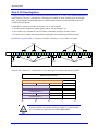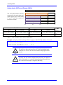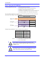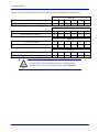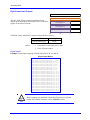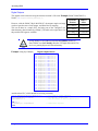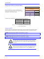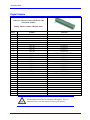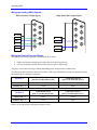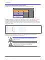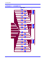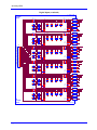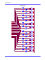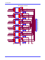
1
^1 USER MANUAL ^2 Accessory 65M ^3 UR Protected/OPTO (Sourcing 24 in 24 out) ^4 3Ax-603740-xUxx ^5November 19, 2013 Single Source Machine Control ……………………………………………..…...………………. Power // Flexibility // Ease of Use 21314 Lassen St. Chatsworth, CA 91311 // Tel. (818) 998-2095 Fax. (818) 998-7807 // www.deltatau.com Copyright Information © 2013 Delta Tau Data Systems, Inc. All rights reserved. This document is furnished for the customers of Delta Tau Data Systems, Inc. Other uses are unauthorized without written permission of Delta Tau Data Systems, Inc. Information contained in this manual may be updated from time-to-time due to product improvements, etc., and may not conform in every respect to former issues. To report errors or inconsistencies, call or email: Delta Tau Data Systems, Inc. Technical Support Phone: (818) 717-5656 Fax: (818) 998-7807 Email: [email protected] Website: http://www.deltatau.com Operating Conditions All Delta Tau Data Systems, Inc. motion controller products, accessories, and amplifiers contain static sensitive components that can be damaged by incorrect handling. When installing or handling Delta Tau Data Systems, Inc. products, avoid contact with highly insulated materials. Only qualified personnel should be allowed to handle this equipment. In the case of industrial applications, we expect our products to be protected from hazardous or conductive materials and/or environments that could cause harm to the controller by damaging components or causing electrical shorts. When our products are used in an industrial environment, install them into an industrial electrical cabinet or industrial PC to protect them from excessive or corrosive moisture, abnormal ambient temperatures, and conductive materials. If Delta Tau Data Systems, Inc. products are directly exposed to hazardous or conductive materials and/or environments, we cannot guarantee their operation. A Warning identifies hazards that could result in personal injury or death. It precedes the discussion of interest. WARNING A Caution identifies hazards that could result in equipment damage. It precedes the discussion of interest. Caution A Note identifies information critical to the understanding or use of the equipment. It follows the discussion of interest. Note Accessory 65M REVISION HISTORY REV. DESCRIPTION DATE CHG APPVD 1 Update manual for new release: new 24 V connector 2/20/07 C.P R.N 2 Updated 16-bit ADC option 12/9/09 C.P S.F 3 Completely revised manual 12/17/12 DCDP R.N 4 Reformatted entire manual Added Power PMAC3/PMAC2 11/15/2013 R.N R.N Accessory 65M Table of Contents INTRODUCTION .....................................................................................................................6 SPECIFICATIONS ...................................................................................................................7 Part Number ................................................................................................................................7 Environmental Specifications ......................................................................................................8 Electrical Specifications ..............................................................................................................8 Physical layout, Mounting ...........................................................................................................9 USING THE ACC-65M WITH POWER PMAC3 ................................................................ 10 Step 1: Preparing the Ring Controller ........................................................................................ 11 Step 2: MACRO ASCII Communication ................................................................................... 13 Step 3: Finishing up the ACC-65M Setup.................................................................................. 15 Step 4: I/O Data Registers ......................................................................................................... 16 Step 5: Using the ACC-65M Data ............................................................................................. 17 Digital Inputs and Outputs.................................................................................................... 19 Analog Inputs (ADCs) and Outputs (DACs) .......................................................................... 20 Using the ADCs for Servo Feedback ..................................................................................... 22 General Purpose Relay Outputs............................................................................................ 23 USING THE ACC-65M WITH POWER PMAC2 ................................................................ 25 Step 1: Preparing the Ring Controller ........................................................................................ 26 Step 2: MACRO ASCII Communication ................................................................................... 27 Step 3: Finishing up the ACC-65M Setup.................................................................................. 29 Step 4: I/O Data Registers ......................................................................................................... 30 Step 5: Using the ACC-65M Data ............................................................................................. 31 Digital Inputs and Outputs.................................................................................................... 33 Analog Inputs (ADCs) and Outputs (DACs) .......................................................................... 35 Using the ADCs for Servo Feedback ..................................................................................... 38 General Purpose Relays ....................................................................................................... 39 USING THE ACC-65M WITH TURBO PMAC2 ................................................................. 41 Step 1: Preparing the Ring Controller ........................................................................................ 42 Step 2: MACRO ASCII Communication ................................................................................... 44 Step 3: Finishing up the ACC-65M Setup.................................................................................. 46 Step 4: I/O Data Registers ......................................................................................................... 47 Nodes and Addressing .......................................................................................................... 47 Turbo Ring Controller I/O Node Registers............................................................................ 48 Step 5: Using the ACC-65M Data ............................................................................................. 49 Digital Inputs and Outputs.................................................................................................... 49 Analog Inputs (ADCS) .......................................................................................................... 52 Introduction 4 Accessory 65M Using the ADCs for Servo Feedback ..................................................................................... 54 Analog Outputs (DACs) ........................................................................................................ 55 General Purpose Relay Outputs............................................................................................ 57 CONNECTOR PINOUTS AND WIRING ............................................................................. 59 24 VDC Input ........................................................................................................................... 59 Digital Inputs ............................................................................................................................ 60 Wiring the digital Inputs ....................................................................................................... 61 Digital Outputs.......................................................................................................................... 62 Wiring the digital outputs ..................................................................................................... 63 Analog Connector ..................................................................................................................... 64 Wiring the Analog (ADC) Inputs........................................................................................... 65 Wiring the Analog (DAC) Outputs ........................................................................................ 66 Wiring the General Purpose Relays ...................................................................................... 66 MACRO Connection ................................................................................................................. 68 Universal Serial Bus (USB) ....................................................................................................... 69 TROUBLESHOOTING .......................................................................................................... 70 Initializing the ACC-65M, Clearing Faults ................................................................................ 70 Error Codes (7-Segment LED) .................................................................................................. 71 LED Status................................................................................................................................ 72 Input and Output LED Indicators ......................................................................................... 72 Status LED ........................................................................................................................... 72 Relay Status LED.................................................................................................................. 72 MACRO Link LED................................................................................................................ 72 APPENDIX A: MEMORY MAP............................................................................................ 73 PMAC3 Style ASIC .................................................................................................................. 73 Using the ACC-65M with PMAC3 Address Offsets ............................................................... 74 PMAC2 Style ASIC .................................................................................................................. 75 Using the ACC-65M with PMAC2 Address Offsets ............................................................... 76 APPENDIX B: E-POINT JUMPERS ..................................................................................... 77 APPENDIX C: SCHEMATICS .............................................................................................. 78 Introduction 5 Accessory 65M INTRODUCTION The accessory 65M (ACC-65M) is a boxed MACRO peripheral I/O module with 24 isolated, self-protected, digital inputs and 24 isolated, self-protected, digital outputs. The ACC-65M is typically configured as a slave in a MACRO ring via either fiber optic or RJ45 connection. The inputs can be either sinking or sourcing depending on the user’s wiring. The outputs are strictly sourcing up to 600 mA per channel. Optional sets of two analog inputs, two analog outputs and two general purpose relay contacts are available. The ACC-65M is compatible with the following Delta Tau controllers: All Turbo PMAC2 board-level MACRO cards Turbo PMAC2 Ethernet Ultralite Power or Turbo UMAC with ACC-5E Power or Turbo Brick family (equipped with the MACRO option) Power UMAC with ACC-5E3 Power PMAC EtherLite Introduction 6 Accessory 65M SPECIFICATIONS Part Number D G K L ACC-65M 4 - 3 7 4 0 - 0 0 - D 0 0 - 0 0 0 K G A - Fiber-Optic MACRO Transceiver 0 - No Option C - RJ-45 MACRO Connector 2 - Two relay contact outputs Two 12-bit bipolar DAC outputs (±10 Volts) Two 16-bit bipolar ADC inputs (± 32767 Counts) MACRO Communication Options L 00 - No Additional* Options xx - FactoryHassigned digits for Additional* Options Factory Assigned Options MACRO Node Options The possible part number configurations are: Options Part Number Fiber optic connectors 4-3740-00-A000-00000 RJ-45 connectors 4-3740-00-C000-00000 Fiber optic connectors 2 x 16-bit bipolar ADC analog inputs (±10 VDC) 2 x 12-bit bipolar DAC analog outputs (±10 VDC) 2 x general purpose relay contacts 4-3740-00-A002-00000 RJ-45 connectors 2 x 16-bit bipolar ADC analog inputs (±10 VDC) 2 x 12-bit bipolar DAC analog outputs (±10 VDC) 2 x general purpose relay contacts 4-3740-00-C002-00000 Note Specifications Revisions 101 and older of the ACC-65M could only support the 12bit ADC inputs which allowed the user to have ± 2047 counts of resolution. The 16-bit ADCs provide ± 32767 counts. 7 Accessory 65M Environmental Specifications Description Specification Operating Temperature 0 °C to 50 °C Storage Temperature Humidity Notes -25 °C to 70 °C 5% to 95% Non-Condensing Relative Humidity Electrical Specifications Logic Power Required Voltage Current Requirements Permitted Time at Peak Current 24 VDC 1.5 A 2 seconds Digital Inputs Voltage Range Continuous Current Rating Peak Current Rating Permitted Time at Peak Current Direction 12 – 24 VDC 1 Amp per channel 2 Amps per channel 2 seconds Sourcing or Sinking (see wiring samples) Digital Outputs Voltage Range Continuous Current Rating Peak Current Rating Permitted Time at Peak Current 0 – 24 VDC 600 mA per channel 1.2 Amps per channel 2 seconds Analog Inputs Maximum Input Voltage Range Resolution 16-bit ADC Chip 12-bit ADC Chip (Rev 1 and older) ± 10 V 16 bits Burr Brown ADS8361E Burr Brown ADS7861E Analog Outputs Maximum Output Voltage Range Output Polarity Resolution DAC Type ± 10 V Bipolar 12 bits Filtered PWM Specifications 8 Accessory 65M Physical layout, Mounting 2.00" (50.8) 6.50" (165.1 mm) 1.00" (25.4) 0.188" (4.760) 6.25" (158.75) 9.75" (247.65 mm) 0.5" (12.7) Specifications 8.625" (219.075 mm) 9.375" (238.13 mm) 1.25" (31.75) 9 Accessory 65M USING THE ACC-65M WITH POWER PMAC3 A Power PMAC3 Style MACRO Ring Controller can be one of the following hardware: Power UMAC with ACC-5E3 Power EtherLite Power Brick (equipped with MACRO) Power Brick AC, Power Brick LV, Power Brick Controller The first step into setting up the ACC-65M is to make sure that the MACRO cables are plugged-in in the correct manner. The OUT from the Ring Controller or previous device goes into the IN of the ACC-65M. The IN of the ACC-65M goes into the OUT of the ring controller or the next device on the ring. For example, the illustration below shows how a MACRO ring with three ACC-65Ms is typically connected: IN OUT STN = 2 IN OUT OUT IN STN = 3 STN = 1 OUT IN Ring Controller The MACRO link LED must be green on all the devices in the MACRO ring for the software setup to work properly. Note Using the ACC-65M with Power PMAC3 10 Accessory 65M Step 1: Preparing the Ring Controller The Power PMAC used to control a MACRO ring must be configured as a ring controller in order to establish communication and transfer data over the ring. Following, is a summary list of the relevant parameters which need to be set properly on the Ring Controller side to allow proper functionality of the MACRO ring, and configuration of the ACC-65M. Structure Element Sys.ClockSource (Set by Firmware) Gate3[i].PhaseFreq Gate3[i].ServoClockDiv Sys.ServoPeriod = 1000*(Gate3[i].ServoClockDiv+1)/Gate3[i].PhaseFreq Sys.PhaseOverServoPeriod = 1/(Gate3[i].ServoClockDiv+1) Sys.RtIntPeriod Macro.TestPeriod Macro.TestMaxErrors = Macro.TestPeriod / 10 Macro.TestReqdSynchs = Macro.TestPeriod – Macro.TestMaxErrors Gate3[i].MacroModeA Gate3[i].MacroModeB Gate3[i].MacroEnableA Gate3[i].MacroEnableB Typical Setting 48 9000 3 0.442 0.250 0 20 2 18 $403000 $1000 $iFC00000 $(i+1)F800000 The Power PMAC can interface to up to 16 PMAC3 Style MACRO ICs. Note Detailed description of these parameters can be found in the pertaining Ring Controller Hardware Reference/User manual or in the Power SRM (Software Reference Manual). These settings require a SAVE followed by a reset $$$ to take effect. Note Once implemented, these settings should ensure that the Power PMAC is now a MACRO ring Controller. And the MACRO Status window in the Power PMAC IDE software should look like: Using the ACC-65M with Power PMAC3 11 Accessory 65M Using the ACC-65M with Power PMAC3 12 Accessory 65M Step 2: MACRO ASCII Communication There are two possible MACRO communication methods between the ring controller and the ACC-65M: MACRO ASCII communication Direct communication to the ACC-65M; it is useful for initial setup, troubleshooting, and allows to eventually establish Master Slave (MS) communication. Master Slave (MS) communication Establishing MS commands (through an I/O node) is ultimately what we want. Note Note Note Make sure that the watch window does not contain any MS{} commands prior to establishing Master Slave communication. This will latch a MACRO communication error (MACRO Status window). If the ACC-65M is to be inserted into an existing MACRO ring system. It may be more practical to place it in a MACRO ring all by itself with the ring controller. Set up and save all the necessary parameters, and then place it back into the system with the other devices. If the ACC-65M has been initialized and set up previously then it may have a station number saved to it. If you know that number (e.g. I11=1), then you would address it with the command MacroStation1. If the ACC65M is at factory default settings then the user needs to issue a MacroStation255. This command searches the MACRO ring for new and unassigned devices. If successful, the AsciiCom status bit is highlighted in the MACRO status window: Now, you are talking directly to the ACC-65M. You should be able to issue commands such as type TYPE, version VERS etc… Using the ACC-65M with Power PMAC3 13 Accessory 65M The goal of MACRO ASCII communication is to enable a selected I/O node over which Master Slave communication can then be used to set up the rest of the necessary parameters of the ACC-65M. Choosing I/O node #2 as an example, enabling it is done through I996: One I/O node is sufficient for transferring all the data available on the ACC-65M. Note Issue a MacroStationClose to terminate MACRO ASCII communication: Using the ACC-65M with Power PMAC3 14 Accessory 65M Step 3: Finishing up the ACC-65M Setup Having enabled a selected I/O node on ACC-65M (i.e. node 2), the corresponding I/O node should be enabled on the ring controller side. For example, at MACRO IC 0, Bank A, node 2: Gate3[0].MacroEnableA = Gate3[0].MacroEnableA | $400 Master Slave communication should be now available over I/O node 2. And the following parameters can be downloaded from the project editor. For example, station number 1 and I/O node 2: MS2,I11=1 // Station number assignment (user configurable) for future // MACRO ASCII communication (e.g. MACSTA1) MS2,I992=6527 MS2,I997=0 // See euqation below // See equation below MS2,I995=$4080 MS2,I996=$0F8004 // Typical setting for MACRO slave device // Nodes enabling, e.g. I/O node #2 MS2,I8=181 MS2,I9=28 MS2,I10=153 // Ring check period (see equation below) // Maximum ring error count (see equation below) // Minimum synch packet count (see equation below) MS{}, I992, and I997 are set so that the phase frequency is the same as the ring controller: 117964.8 1000 MS2, I992 Ceil 3 2 Gate3[i].PhaseFreq // Where ceil is rounding to the higher integer MS2, I997 Gate3[ i].PhaseClo ckDiv If the clock settings are not at default, MS{},I8, I9, and I10 can be calculated using the following equations. Assuming a typical ring check period (RingCheckPeriod) of 20 milliseconds and a fatal packet error (MaxErrorPercent) of 15 percent: (Ringcheck Period 117964.8) (MS2, I997 1) MS2, I8 INT 1 (2 MS2, I992 3) (MS2, I8 MaxErrorPe rcent) MS2, I9 INT 1 100 MS2, I10 MS2, I8 MS2, I9 These equations must be computed ahead of time, expressions cannot be written directly into MS{} variables. Note These settings must be retained on the ACC65M. This is done by issuing a save (e.g. MSSAVE2), followed by a reset (e.g. MS$$$2) to take effect: Using the ACC-65M with Power PMAC3 15 Accessory 65M Step 4: I/O Data Registers A single I/O node is sufficient for transferring the data to/from the ACC-65M. This is handled automatically in the firmware. The user’s responsibility is choosing an available I/O node, enabling it per the example above, and finding the corresponding register or data element structure (listed in the tables below) for reading/writing to the data. A MACRO IC consists of a number of auxiliary, servo, and I/O nodes: Auxiliary nodes are Master/Control registers and for internal firmware use. Servo nodes carry information such as feedback, commands, and flags for motor control. I/O nodes are by default unoccupied and are configurable for transferring miscellaneous data. Each PMAC3 style MACRO IC consists of 32 nodes: 4 auxiliary, 16 servo, and 12 I/O nodes: I/O Nodes Node 15 14 13 12 11 10 Auxiliary Nodes 9 8 7 I/O Nodes 6 5 4 3 2 1 0 15 14 13 12 11 Auxiliary Nodes Servo Nodes 10 9 8 7 6 5 4 3 2 Servo Nodes Bank B Bank A Each I/O node consists of 1 x 24-bit and 3 x 16-bit data registers residing in the following fields: PMAC3 Style I/O Node 24-bit Register 16-bit Register 1 16-bit Register 2 16-bit Register 3 31 23 15 7 0 The Power PMAC can interface with up to 16 PMAC3 Style MACRO ICs. ICs present are reported by the variable Macro.IC3s. Note Using the ACC-65M with Power PMAC3 16 1 0 Accessory 65M Step 5: Using the ACC-65M Data Having configured the following: Set up the MACRO ring controller Set up the phase clock to be the same across the ring Enabled a selected I/O node on the ACC-65M Enabled the corresponding I/O node on the ring controller side Saved and reset both the ACC-65M and the ring controller The ACC-65M data should now be available to access from the ring controller side. The ACC-65M firmware places the data automatically in the following data registers of a selected I/O node: PMAC3 Style I/O Node Digital I/O 24-bit Register 16-bit Register 1 Analog I/O 16-bit Register 2 GP Relays 16-bit Register 3 31 23 15 7 0 And each I/O node possesses data structure elements for inputs and outputs separately for either bank: Bank B Bank A Inputs Outputs Inputs Outputs Data Register Gate3[i].MacroInB[j][0] Gate3[i].MacroOutB[j][0] Gate3[i].MacroInA[j][0] Gate3[i].MacroOutA[j][0] 24-bit Gate3[i].MacroInB[j][1] Gate3[i].MacroOutB[j][1] Gate3[i].MacroInA[j][1] Gate3[i].MacroOutA[j][1] 1st 16-bit Gate3[i].MacroInB[j][2] Gate3[i].MacroOutB[j][2] Gate3[i].MacroInA[j][2] Gate3[i].MacroOutA[j][2] 2nd 16-bit Gate3[i].MacroInB[j][3] Gate3[i].MacroOutB[j][3] Gate3[i].MacroInA[j][3] Gate3[i].MacroOutA[j][3] 3rd 16-bit Where: i is the PMAC3 Style MACRO IC index j is the I/O node number. Note Bitwise mapping, and signed assignments into the PMAC3 Style MACRO structure elements require Power PMAC firmware version 1.5.8.305 or newer. Using the ACC-65M with Power PMAC3 17 Accessory 65M Power PMAC firmware versions older than 1.5.8.305 must use explicit address offsets found in the memory map appendix section. Note Below, are example tables showing I/O Node numbers of the first 4 PMAC3 Style MACRO ICs: Gate3[0] Bank A Bank B ACC-65M I/O Node# 2 3 6 7 10 11 2 3 6 7 11 12 Ring Controller I/O Node [j] 2 3 6 7 10 11 18 19 22 23 26 27 Gate3[1] Bank A Bank B ACC-65M I/O Node# 2 3 6 7 10 11 2 3 6 7 11 12 Ring Controller I/O Node [j] 34 35 38 39 42 43 50 51 54 55 58 59 Gate3[2] Bank A Bank B ACC-65M I/O Node# 2 3 6 7 10 11 2 3 6 7 11 12 Ring Controller I/O Node [j] 66 67 70 71 74 75 82 83 86 87 90 91 Gate3[3] Bank A Bank B ACC-65M I/O Node# 2 3 6 7 10 11 2 3 6 7 11 12 Ring Controller I/O Node [j] 98 99 102 103 106 107 114 115 118 119 122 123 Using the ACC-65M with Power PMAC3 18 Accessory 65M Digital Inputs and Outputs PMAC3 Style I/O Node The ACC-65M firmware transfers automatically the digitals inputs and outputs into/from the upper 24 bits of the 24-bit data register of the chosen I/O node. ACC-65M Digital Inputs / Outputs 16-bit Register 1 16-bit Register 2 16-bit Register 3 31 23 15 Bank B Inputs Bank A Outputs Gate3[i].MacroInB[j][0] 7 Inputs Outputs Gate3[i].MacroOutB[j][0] Gate3[i].MacroInA[j][0] Gate3[i].MacroOutA[j][0] 0 Data Register 24-bit Where: i is the card index, and j is the I/O node number Example: Digital I/O mapping at MACRO IC 0, Bank A, I/O node 2 Digital Outputs Bitwise PTR PTR PTR PTR PTR PTR PTR PTR PTR PTR PTR PTR PTR PTR PTR PTR PTR PTR PTR PTR PTR PTR PTR PTR Output1->Gate3[0].MacroOutA[2][0].8.1; Output2->Gate3[0].MacroOutA[2][0].9.1; Output3->Gate3[0].MacroOutA[2][0].10.1; Output4->Gate3[0].MacroOutA[2][0].11.1; Output5->Gate3[0].MacroOutA[2][0].12.1; Output6->Gate3[0].MacroOutA[2][0].13.1; Output7->Gate3[0].MacroOutA[2][0].14.1; Output8->Gate3[0].MacroOutA[2][0].15.1; Output9->Gate3[0].MacroOutA[2][0].16.1; Output10->Gate3[0].MacroOutA[2][0].17.1; Output11->Gate3[0].MacroOutA[2][0].18.1; Output12->Gate3[0].MacroOutA[2][0].19.1; Output13->Gate3[0].MacroOutA[2][0].20.1; Output14->Gate3[0].MacroOutA[2][0].21.1; Output15->Gate3[0].MacroOutA[2][0].22.1; Output16->Gate3[0].MacroOutA[2][0].23.1; Output17->Gate3[0].MacroOutA[2][0].24.1; Output18->Gate3[0].MacroOutA[2][0].25.1; Output19->Gate3[0].MacroOutA[2][0].26.1; Output20->Gate3[0].MacroOutA[2][0].27.1; Output21->Gate3[0].MacroOutA[2][0].28.1; Output22->Gate3[0].MacroOutA[2][0].29.1; Output23->Gate3[0].MacroOutA[2][0].30.1; Output24->Gate3[0].MacroOutA[2][0].31.1; Using the ACC-65M with Power PMAC3 Digital Inputs Bitwise PTR PTR PTR PTR PTR PTR PTR PTR PTR PTR PTR PTR PTR PTR PTR PTR PTR PTR PTR PTR PTR PTR PTR PTR Input1->Gate3[0].MacroInA[2][0].8.1; Input2->Gate3[0].MacroInA[2][0].9.1; Input3->Gate3[0].MacroInA[2][0].10.1; Input4->Gate3[0].MacroInA[2][0].11.1; Input5->Gate3[0].MacroInA[2][0].12.1; Input6->Gate3[0].MacroInA[2][0].13.1; Input7->Gate3[0].MacroInA[2][0].14.1; Input8->Gate3[0].MacroInA[2][0].15.1; Input9->Gate3[0].MacroInA[2][0].16.1; Input10->Gate3[0].MacroInA[2][0].17.1; Input11->Gate3[0].MacroInA[2][0].18.1; Input12->Gate3[0].MacroInA[2][0].19.1; Input13->Gate3[0].MacroInA[2][0].20.1; Input14->Gate3[0].MacroInA[2][0].21.1; Input15->Gate3[0].MacroInA[2][0].22.1; Input16->Gate3[0].MacroInA[2][0].23.1; Input17->Gate3[0].MacroInA[2][0].24.1; Input18->Gate3[0].MacroInA[2][0].25.1; Input19->Gate3[0].MacroInA[2][0].26.1; Input20->Gate3[0].MacroInA[2][0].27.1; Input21->Gate3[0].MacroInA[2][0].28.1; Input22->Gate3[0].MacroInA[2][0].29.1; Input23->Gate3[0].MacroInA[2][0].30.1; Input24->Gate3[0].MacroInA[2][0].31.1; 19 Accessory 65M Analog Inputs (ADCs) and Outputs (DACs) PMAC3 Style I/O Node 24-bit Register The ACC-65M firmware transfers automatically the analog inputs and outputs from/to upper 16 bits of the 1st and 2nd 16-bit data registers of the chosen I/O node. ACC-65M ADC 1 / DAC 1 ACC-65M ADC 2 / DAC 2 16-bit Register 3 31 23 15 Bank B 7 Bank A 0 Inputs Outputs Inputs Outputs Data Register Gate3[i].MacroInB[j][1] Gate3[i].MacroOutB[j][1] Gate3[i].MacroInA[j][1] Gate3[i].MacroOutA[j][1] 1st 16-bit Gate3[i].MacroInB[j][2] Gate3[i].MacroOutB[j][2] Gate3[i].MacroInA[j][2] Gate3[i].MacroOutA[j][2] 2nd 16-bit Where: i is the card index, and j is the I/O node number Example: Analog Input ADCs and output DACs mapping at MACRO IC 0, Bank A, I/O node 2 PTR ADC1->Gate3[0].MacroInA[2][1].16.16S; PTR ADC2->Gate3[0].MacroInA[2][2].16.16S; // ADC #1 // ADC #2 PTR DAC1->Gate3[0].MacroOutA[2][1].16.16S; PTR DAC2->Gate3[0].MacroOutA[2][2].16.16S; // DAC #1 // DAC #1 Note Note The ADCs on older revisions of the ACC-65M (2-pin Molex logic connector) are 12 bits. The suffix of the address mapping should be .12.12S Typically, the ACC-65M is configured (by the factory) for unsigned data. Occasionally, it is ordered in the unsigned data format. Remove the S in the suffix for proper “unsigned” addressing. Using the ACC-65M with Power PMAC3 20 Accessory 65M Testing the Analog Inputs Applying a voltage into the physical input pins, and reading the above referenced pointers for unsigned (unipolar) or signed (bipolar) data, the user should see the following. With the 16-bit ADCs: Unipolar Single-Ended Signal [VDC] Differential Signal [VDC] Software Counts -10 -5 -32768 0 0 0 10 5 32768 Single-Ended Signal [VDC] Differential Signal [VDC] Software Counts -10 -5 -2048 0 0 0 10 5 2048 Bipolar With the 12-bit ADCs: Unipolar Bipolar Testing the Analog Outputs These are ±10V outputs, where 10 volts corresponds to the value of MS2,I992. Remember that this is dictated by the ring phase clock, do not attempt to change it in this section. Pointer For example, with the default clock setting (e.g. MS2,I992=6527) and by writing to the analog output data register or suggested pointer, the user should see: Using the ACC-65M with Power PMAC3 -6527 -3264 0 3264 6527 Single Ended [VDC] -10 -5 0 +5 +10 Differential [VDC] -20 -10 0 +10 +20 21 Accessory 65M Using the ADCs for Servo Feedback Using an analog ADC input for servo requires bringing it into the encoder conversion table (ECT). Using the automatic ECT utility in the IDE software: Type: Single 32-bit register read Source Address: I/O node structure element address (i.e. Gate3[i].MacroInA[j][1]) LSB Bit#: starting bit of ADC data (typically 16) #of Bits Used: ADC data number of bits (16 or 12) Result Units: set to 1 to shift data 16 bits for proper scaling Alternately, using the ECT structure elements: EncTable[1].type = 1 EncTable[1].pEnc = Gate3[0].MacroInA[2][1].a EncTable[1].index1 = 16 EncTable[1].index2 = 16 EncTable[1].index3 = 0 EncTable[1].index4 = 0 EncTable[1].index5 = 0 EncTable[1].ScaleFactor = 1 / EXP2(16) The ADC data is now processed in the encoder conversion table. A motor element structure can point to it. Example: Motor[1].pMasterEnc = EncTable[1].a Or it can be accessed manually using a pointer. Note that you would need to multiply by the scale factor (or divide by 2^16 in this example) for proper scaling. Example: PTR ECT1Result->EncTable[1].PrevEnc Using the ACC-65M with Power PMAC3 22 Accessory 65M General Purpose Relay Outputs PMAC3 Style I/O Node 24-bit Register The ACC-65M firmware transfers automatically the general purpose relay outputs 1 and 2 into bits 27 and 28 respectively of the 3rd 16-bit I/O data register. 16-bit Register 1 16-bit Register 2 GP Relays Bits 27, and 28 31 23 15 Bank B 7 Bank A 0 Inputs Outputs Inputs Outputs Data Register Gate3[i].MacroInB[j][3] Gate3[i].MacroOutB[j][3] Gate3[i].MacroInA[j][3] Gate3[i].MacroOutA[j][3] 3rd 16-bit Bank B Bank A Example: General purpose relay outputs mapping at MACRO IC 0, both banks, and all nodes: I/O GP Relay #1 GP Relay #2 2 PTR GpRelay1->Gate3[0].MacroOutA[2][3].27.1 PTR GpRelay2->Gate3[0].MacroOutA[2][3].28.1 3 PTR GpRelay1->Gate3[0].MacroOutA[3][3].27.1 PTR GpRelay2->Gate3[0].MacroOutA[3][3].28.1 6 PTR GpRelay1->Gate3[0].MacroOutA[6][3].27.1 PTR GpRelay2->Gate3[0].MacroOutA[6][3].28.1 7 PTR GpRelay1->Gate3[0].MacroOutA[7][3].27.1 PTR GpRelay2->Gate3[0].MacroOutA[7][3].28.1 10 PTR GpRelay1->Gate3[0].MacroOutA[10][3].27.1 PTR GpRelay2->Gate3[0].MacroOutA[10][3].28.1 11 PTR GpRelay1->Gate3[0].MacroOutA[11][3].27.1 PTR GpRelay2->Gate3[0].MacroOutA[11][3].28.1 2 PTR GpRelay1->Gate3[0].MacroOutB[2][3].27.1 PTR GpRelay2->Gate3[0].MacroOutB[2][3].28.1 3 PTR GpRelay1->Gate3[0].MacroOutB[3][3].27.1 PTR GpRelay2->Gate3[0].MacroOutB[3][3].28.1 6 PTR GpRelay1->Gate3[0].MacroOutB[6][3].27.1 PTR GpRelay2->Gate3[0].MacroOutB[6][3].28.1 7 PTR GpRelay1->Gate3[0].MacroOutB[7][3].27.1 PTR GpRelay2->Gate3[0].MacroOutb[7][3].28.1 10 PTR GpRelay1->Gate3[0].MacroOutB[10][3].27.1 PTR GpRelay2->Gate3[0].MacroOutB[10][3].28.1 11 PTR GpRelay1->Gate3[0].MacroOutB[11][3].27.1 PTR GpRelay2->Gate3[0].MacroOutB[11][3].28.1 Using the ACC-65M with Power PMAC3 23 Accessory 65M Testing the General Purpose Relays The following table summarizes the relay functions. That is the relationship between the common line and the normally open / normally closed lines: GP Relay 1 Connection between pins #13 (COM) and #14 (NO) Connection between pins #13 (COM) and #6 (NC) Software bit = 0 Open Closed Software bit = 1 Closed Open GP Relay 2 Connection between pins #7 (COM) and #8 (NO) Connection between pins #7 (COM) and #15 (NC) Software bit = 0 Open Closed Software bit = 1 Closed Open Using the ACC-65M with Power PMAC3 24 Accessory 65M USING THE ACC-65M WITH POWER PMAC2 A Power PMAC2 Style MACRO Ring Controller is comprised of a Power UMAC with one or more ACC5Es in the rack. The first step into setting up the ACC-65M is to make sure that the MACRO cables are plugged-in in the correct manner. The OUT from the Ring Controller or previous device goes into the IN of the ACC-65M. The IN of the ACC-65M goes into the OUT of the ring controller or the next device on the ring. For example, the illustration below shows how a MACRO ring with three ACC-65Ms is typically connected: OUT IN STN = 2 IN OUT OUT IN STN = 3 OUT STN = 1 IN Ring Controller The MACRO link LED must be green on all the devices in the MACRO ring for the software setup to work properly. Note The Power UMAC with ACC-5E is the only configuration in which a Power PMAC interfaces to a PMAC2 Style MACRO IC. Note Using the ACC-65M with Power PMAC2 25 Accessory 65M Step 1: Preparing the Ring Controller The Power PMAC used to control a MACRO ring must be configured as a ring controller in order to establish communication and transfer data over the ring. Following, is a summary list of the relevant structure elements which need to be set properly on the Ring Controller side to allow proper functionality of the MACRO ring, and configuration of the ACC-65M: Structure element Typical Setting Gate2[i].PhaseClockDiv Gate2[i].ServoClockDiv Sys.ServoPeriod=(2*Gate2[i].PwmPeriod+3)*(Gate2[i].PhaseClockDiv+1)*(Gate2[i].ServoClockDiv+1)/117964.8 32 6527 0 3 0.442 Sys.ClockSource (Set by Firmware) Gate2[i].PwmPeriod Sys.PhaseOverServoPeriod=1/(Gate2[i].ServoClockDiv+1) Sys.RtIntPeriod Macro.TestPeriod Macro.TestMaxErrors = Macro.TestPeriod / 10 Gate2[i].MacroMode Gate2[i].MacroEnable 0.250 0 20 2 $4030 $iFC000 Where i is the ACC-5E (Gate2[i]) index. Detailed description of these parameters can be found in the pertaining Ring Controller Hardware Reference/User manual or in the Power SRM (Software Reference Manual). The Power PMAC can interface with up to 32 PMAC2 Style MACRO ICs or up to 8 fully populated ACC-5Es. Note These settings require a SAVE followed by a reset $$$ to take effect. Note Once implemented, these settings should ensure that the Power PMAC is now a MACRO ring Controller. And the MACRO Status window in the Power PMAC IDE software should look like: Using the ACC-65M with Power PMAC2 26 Accessory 65M Step 2: MACRO ASCII Communication There are two possible MACRO communication methods between the ring controller and the ACC-65M: MACRO ASCII communication Direct communication to the ACC-65M; it is useful for initial setup, troubleshooting, and allows to eventually establish Master Slave (MS) communication. Master Slave (MS) communication Establishing MS commands (through an I/O node) is ultimately what we want. Note Note Note Make sure that the watch window does not contain any MS{} commands prior to establishing Master Slave communication. This will latch a MACRO communication error (MACRO Status window). If the ACC-65M is to be inserted into an existing MACRO ring system. It may be more practical to place it in a MACRO ring all by itself with the ring controller. Set up and save all the necessary parameters, and then place it back into the system with the other devices. If the ACC-65M has been initialized and set up previously then it may have a station number saved to it. If you know that number (e.g. I11=1), then you would address it with the command MacroStation1. If the ACC65M is at factory default settings then the user needs to issue a MacroStation255. This command searches the MACRO ring for new and unassigned devices. If successful, the AsciiCom status bit is highlighted in the MACRO status window: Now, you are talking directly to the ACC-65M. You should be able to issue commands such as type TYPE, version VERS etc… Using the ACC-65M with Power PMAC2 27 Accessory 65M The goal of MACRO ASCII communication is to enable a selected I/O node over which Master Slave communication can be used to set up the rest of the necessary parameters of the ACC-65M. Choosing I/O node #2 as an example, enabling it is done through I996: One I/O node is sufficient for transferring all the data available on the ACC-65M. Note Issue a MacroStationClose to terminate MACRO ASCII communication: Using the ACC-65M with Power PMAC2 28 Accessory 65M Step 3: Finishing up the ACC-65M Setup Having enabled a selected I/O node on ACC-65M through MACRO ASCII (i.e. node 2), the corresponding I/O node should be enabled on the ring controller side. For example at MACRO IC 0: Gate2[0].MacroEnable = Gate2[0].MacroEnable | $4 Master Slave communication should be now available over I/O node 2. And the following parameters can be downloaded from the project editor. For example, station number 1 and I/O node 2: MS2,I11=1 // Station number assignment (user configurable) for future // MACRO ASCII communication (e.g. MACSTA1) MS2,I992=6527 MS2,I997=0 // See below // See below MS2,I995=$4080 MS2,I996=$0F8004 // Typical setting for MACRO slave device // Nodes enabling, e.g. I/O node #2 MS2,I8=181 MS2,I9=28 MS2,I10=153 // Ring check period (see equation below) // Maximum ring error count (see equation below) // Minimum synch packet count (see equation below) MS{}, I992, and I997 are set so that the phase frequency is the same as the ring controller: MS2, I992 Gate2[0].P wmPeriod MS2, I997 Gate2[0].P haseClockD iv If the clock settings are not at default, MS{},I8, I9, and I10 can be calculated using the following equations. Assuming a typical ring check period (RingCheckPeriod) of 20 milliseconds and a fatal packet error (MaxErrorPercent) of 15 percent: (Ringcheck Period 117964.8) (MS2, I997 1) MS2, I8 INT 1 (2 MS2, I992 3) (MS2, I8 MaxErrorPe rcent) MS2, I9 INT 1 100 MS2, I10 MS2, I8 MS2, I9 These equations must be computed explicitly ahead of time, expressions cannot be written directly into MS{} variables. Note These settings must be retained on the ACC-65M. This is done by issuing a save (e.g. MSSAVE2), followed by a reset (e.g. MS$$$2) to take effect: Using the ACC-65M with Power PMAC2 29 Accessory 65M Step 4: I/O Data Registers A single I/O node is sufficient for transferring the data to/from the ACC-65M. This is handled automatically in the firmware. The user’s responsibility is choosing an available I/O node, enabling it per the example above, and finding the corresponding register or data element structure (listed in the tables below) for reading/writing to the data. A MACRO IC consists of a number of auxiliary, servo, and I/O nodes: Auxiliary nodes are Master/Control registers and for internal firmware use. Servo nodes carry information such as feedback, commands, and flags for motor control. I/O nodes are by default unoccupied and are configurable for transferring miscellaneous data. Each PMAC2 Style MACRO IC consists of 16 nodes: 2 auxiliary, 8 servo, and 6 I/O nodes: I/O Nodes Node 15 14 13 12 11 10 9 8 Auxiliary Nodes 7 6 5 4 3 2 1 0 Servo Nodes Each I/O node register consists of one 24-bit and three 16-bit data registers placed in the following fields: PMAC2 Style I/O Node 24-bit Register 16-bit Register 1 16-bit Register 2 16-bit Register 3 23 15 7 0 A Power PMAC CPU can interface with up to 32 PMAC2 Style MACRO ICs. ICs present are reported by the variable Macro.ICs Note Using the ACC-65M with Power PMAC2 30 Accessory 65M Step 5: Using the ACC-65M Data Having configured the following: Set up the MACRO ring controller Set up the phase clock to be the same across the ring Enabled a selected I/O node on the ACC-65M Enabled the corresponding I/O node on the ring controller side Saved and reset both the ACC-65M and the ring controller The ACC-65M data should now be available to access from the ring controller side at the specified I/O node with the data residing is in the following fields: PMAC2 Style I/O Node Digital I/O 24-bit Register 16-bit Register 1 Analog I/O 16-bit Register 2 GP Relays 16-bit Register 3 23 15 7 0 The PMAC2 Style MACRO IC structure elements for these registers are: Where: Structure Element Data Register Gate2[i].Macro[j][0] 24-bit Gate2[i].Macro[j][0] 16-bit Gate2[i].Macro[j][0] 16-bit Gate2[i].Macro[j][0] 16-bit i is the PMAC2 Style MACRO IC index j is the I/O node number. Note Bitwise mapping, and signed assignments into the PMAC2 Style MACRO structure elements require Power PMAC firmware version 1.5.8.305 or newer. Power PMAC firmware versions older than 1.5.8.305 must use explicit address offsets found in the memory map appendix section. Note Using the ACC-65M with Power PMAC2 31 Accessory 65M Below, are example tables showing I/O Node numbers of the first 4 PMAC2 Style MACRO ICs: Gate2[0] ACC-65M I/O Node# 2 3 6 7 10 11 Ring Controller I/O Node [j] 2 3 6 7 10 11 Gate2[1] ACC-65M I/O Node# 2 3 6 7 11 12 Ring Controller I/O Node [j] 18 19 22 23 26 27 Gate2[2] ACC-65M I/O Node# 2 3 6 7 10 11 Ring Controller I/O Node [j] 34 35 38 39 42 43 Gate2[3] ACC-65M I/O Node# 2 3 6 7 11 12 Ring Controller I/O Node [j] 50 51 54 55 58 59 A Power PMAC CPU can interface with up to 32 PMAC2 Style MACRO ICs. ICs present are reported by the variable Macro.ICs Note Using the ACC-65M with Power PMAC2 32 Accessory 65M Digital Inputs and Outputs PMAC2 Style I/O Node ACC-65M Digital Inputs / Outputs The ACC-65M firmware transfers automatically the digitals inputs and outputs into/from the lower 24 bit data register of the chosen I/O node. 16-bit Register 1 16-bit Register 2 16-bit Register 3 23 15 7 0 The PMAC2 Style MACRO IC structure element for this register is: Structure Element Data Register Gate2[i].Macro[j][0] 24-bit i is the PMAC2 Style MACRO IC index Where: j is the I/O node number. Digital Inputs Example: Digital inputs mapping at PMAC2 MACRO IC 0, I/O node 2 Digital Inputs Bitwise PTR PTR PTR PTR PTR PTR PTR PTR PTR PTR PTR PTR PTR PTR PTR PTR PTR PTR PTR PTR PTR PTR PTR PTR Input1->Gate2[0].Macro[2][0].0.1; Input2->Gate2[0].Macro[2][0].1.1; Input3->Gate2[0].Macro[2][0].2.1; Input4->Gate2[0].Macro[2][0].3.1; Input5->Gate2[0].Macro[2][0].4.1; Input6->Gate2[0].Macro[2][0].5.1; Input7->Gate2[0].Macro[2][0].6.1; Input8->Gate2[0].Macro[2][0].7.1; Input9->Gate2[0].Macro[2][0].8.1; Input10->Gate2[0].Macro[2][0].9.1; Input11->Gate2[0].Macro[2][0].10.1; Input12->Gate2[0].Macro[2][0].11.1; Input13->Gate2[0].Macro[2][0].12.1; Input14->Gate2[0].Macro[2][0].13.1; Input15->Gate2[0].Macro[2][0].14.1; Input16->Gate2[0].Macro[2][0].15.1; Input17->Gate2[0].Macro[2][0].16.1; Input18->Gate2[0].Macro[2][0].17.1; Input19->Gate2[0].Macro[2][0].18.1; Input20->Gate2[0].Macro[2][0].19.1; Input21->Gate2[0].Macro[2][0].20.1; Input22->Gate2[0].Macro[2][0].21.1; Input23->Gate2[0].Macro[2][0].22.1; Input24->Gate2[0].Macro[2][0].23.1; Bitwise mapping into the PMAC2 Style MACRO structure elements require Power PMAC firmware version 1.5.8.305 or newer. Note Using the ACC-65M with Power PMAC2 33 Accessory 65M Digital Outputs The outputs can be written to using the structure element’s full word. Example: PMAC2 MACRO IC 0, Node 2; PTR Outputs->Gate2[0].Macro[2][0] However, with the PMAC2 Style MACRO IC, the outputs require an image word to report the state of each output, and allow bitwise mapping. This can be done in a simple PLC, and using one of the “unsigned” user shared memory data elements Sys.Udata[i]. The table to the right shows 4 of the possible 65K registers available: Structure Element Address Offset Sys.Udata[4] U.USER:16 Sys.Udata[8] U.USER:32 Sys.Udata[12] U.USER:48 Sys.Udata[16] U.USER:64 Note A large number of self-addressed (default Sys.pushm) pointers in Power PMAC use Sys.Udata[0]; therefore it is highly advised NOT to use it as a general purpose user shared memory. Digital Outputs Bitwise Example: using Sys.Udata[4] PTR PTR PTR PTR PTR PTR PTR PTR PTR PTR PTR PTR PTR PTR PTR PTR PTR PTR PTR PTR PTR PTR PTR PTR Output1->U.USER:16.0.1; Output2->U.USER:16.1.1; Output3->U.USER:16.2.1; Output4->U.USER:16.3.1; Output5->U.USER:16.4.1; Output6->U.USER:16.5.1; Output7->U.USER:16.6.1; Output8->U.USER:16.7.1; Output9->U.USER:16.8.1; Output10->U.USER:16.9.1; Output11->U.USER:16.10.1; Output12->U.USER:16.11.1; Output13->U.USER:16.12.1; Output14->U.USER:16.13.1; Output15->U.USER:16.14.1; Output16->U.USER:16.15.1; Output17->U.USER:16.16.1; Output18->U.USER:16.17.1; Output19->U.USER:16.18.1; Output20->U.USER:16.19.1; Output21->U.USER:16.20.1; Output22->U.USER:16.21.1; Output23->U.USER:16.22.1; Output24->U.USER:16.23.1; And the mirror PLC, which should be executing constantly: PTR IC0_N2Twenty4->Gate2[0].Macro[2][0]; PTR OutputsMirror->U.USER:16; OutputsMirror = 0; // IC 0, Node 2, 24-bit register // Sys.Udata[4], mirror word // Save/Initialize to zero or desired state OPEN PLC 1 IC0_N2Twenty4 = OutputsMirror CLOSE // Update data register Using the ACC-65M with Power PMAC2 34 Accessory 65M Analog Inputs (ADCs) and Outputs (DACs) PMAC2 Style I/O Node 24-bit Register The ACC-65M firmware transfers automatically the analog inputs and outputs from/to the 1st and 2nd 16-bit data registers of the chosen I/O node. ACC-65M ADC 1 / DAC 1 ACC-65M ADC 2 / DAC 2 16-bit Register 3 23 15 7 0 The PMAC2 Style MACRO IC structure elements for these registers are: Where: Structure Element Data Register Gate2[i].Macro[j][1] 1st 16-bit Gate2[i].Macro[j][2] 2nd 16-bit i is the PMAC2 Style MACRO IC index j is the I/O node number. Analog Input ADCs The ADC inputs can be mapped directly into the node’s structure elements, and read directly without further processing. Typically, the ACC-65M is configured (by the factory) for signed ADC inputs. Example: Signed ADC inputs at PMAC2 Style MACRO IC 0, Node 2: PTR ADC1->Gate2[0].Macro[2][1].8.16S // IC 0, Node 2, ADC 1 signed PTR ADC2->Gate2[0].Macro[2][2].8.16S // IC 0, Node 2, ADC 2 signed Example: Unsigned ADC inputs at PMAC2 Style MACRO IC 0, Node 2: PTR ADC1->Gate2[0].Macro[2][1].8.16 PTR ADC2->Gate2[0].Macro[2][2].8.16 Note // IC 0, Node 2, ADC 1 unsigned // IC 0, Node 2, ADC 2 unsigned The ADC inputs on the older revision of the ACC-65M (2-pin Molex logic connector) are 12 bits. The suffix of the address mapping should be 12.12S. Bitwise, and signed mapping into the PMAC2 Style MACRO structure elements require Power PMAC firmware version 1.5.8.305 or newer. Note Using the ACC-65M with Power PMAC2 35 Accessory 65M Analog Output DACs The analog output DACs can be written to using the structure element’s full word. Example: PMAC2 MACRO IC 0, Node 2, DAC 1; PTR DAC1->Gate2[0].Macro[2][1]. However, with the PMAC2 Style MACRO IC, the DAC outputs require an image word to report the value of each output, and allow byte-wise mapping for proper scaling. This can be done in a simple PLC, and using one of the “unsigned” user shared memory data elements Sys.Udata[i]. The table to the right shows 4 of the possible 65K registers available: Note Structure Element Address Offset Sys.Udata[4] U.USER:16 Sys.Udata[8] U.USER:32 Sys.Udata[12] U.USER:48 Sys.Udata[16] U.USER:64 A large number of self-addressed (default Sys.pushm) pointers in Power PMAC use Sys.Udata[0]; therefore it is highly advised NOT to use it as a general purpose user shared memory. Example: Using Sys.Udata[8] for both DACs 1, and 2 PTR DAC1->S.USER:32.0.16 PTR DAC2->S.USER:32.8.16 Note // DAC 1, pointing to signed user shared memory // DAC 2, pointing to signed user shared memory Typically, the ACC-65M is configured (by the factory) for signed DAC outputs. For unsigned DACs, simply replace the S in the prefix of the assignment with a U. And the mirror PLC, which should be executing constantly: PTR N2First16->Gate[2].Macro[2][1] PTR N2Second16->Gate[2].Macro[2][2] OPEN PLC 1 N2First16 = DAC1 * 256 N2Second16 = DAC2 * 256 CLOSE // Node 2, 1st 16-bit data register // Node 2, 2nd 16-bit data register // Update data register, upper 16 // Update data register, upper 16 Using the ACC-65M with Power PMAC2 36 Accessory 65M Testing the Analog Inputs Applying a voltage into the physical input pins, and reading the above referenced pointers for unsigned (unipolar) or signed (bipolar) data, the user should see the following. With the 16-bit ADCs: Unipolar Single-Ended Signal [VDC] Differential Signal [VDC] Software Counts -10 -5 -32768 0 0 0 10 5 32768 Single-Ended Signal [VDC] Differential Signal [VDC] Software Counts -10 -5 -2048 0 0 0 10 5 2048 Bipolar With the 12-bit ADCs: Unipolar Bipolar Testing the Analog Outputs These are ±10V outputs, where 10 volts corresponds to the value of MS2,I992. Remember that this is dictated by the ring phase clock, do not attempt to change it in this section. Pointer For example, with the default clock setting (e.g. MS2,I992=6527) and by writing to the analog output data register or suggested pointer, the user should see: Using the ACC-65M with Power PMAC2 -6527 -3264 0 3264 6527 Single Ended [VDC] -10 -5 0 +5 +10 Differential [VDC] -20 -10 0 +10 +20 37 Accessory 65M Using the ADCs for Servo Feedback Using an analog ADC input for servo requires bringing it into the encoder conversion table (ECT). Using the automatic ECT utility in the IDE software: Type: Single 32-bit register read Source Address: I/O node structure element address (i.e. Gate2[i].Macro[j][1]) LSB Bit#: starting bit of ADC data (typically 16) #of Bits Used: ADC data number of bits (16 or 12) Result Units: set to 1 to shift data 16 bits for proper scaling Alternately, using the ECT structure elements: EncTable[1].type = 1 EncTable[1].pEnc = Gate2[0].Macro[2][1].a EncTable[1].index1 = 16 EncTable[1].index2 = 16 EncTable[1].index3 = 0 EncTable[1].index4 = 0 EncTable[1].index5 = 0 EncTable[1].ScaleFactor = 1 / EXP2(16) The ADC data is now processed in the encoder conversion table. A motor element structure can point to it. Example: Motor[1].pMasterEnc = EncTable[1].a Or it can be accessed manually using a pointer. Note that you would need to multiply by the scale factor (or divide by 2^16 in this example) for proper scaling. Example: PTR ECT1Result->EncTable[1].PrevEnc Using the ACC-65M with Power PMAC2 38 Accessory 65M General Purpose Relays The general purpose relays 1 and 2 are transferred respectively into bits 19 and 20 of the 3rd 16-bit data register of the I/O node. The PMAC2 Style MACRO IC structure element for this register is: Structure Element Data Register Gate2[i].Macro[j][3] 16-bit (middle) Where: i is the PMAC2 Style MACRO IC index j is the I/O node number. With the PMAC2 Style MACRO IC, the GP relay outputs require an image word to report the value of each output, and allow byte-wise mapping. This can be done in a simple PLC, and using one of the “unsigned” user shared memory data elements Sys.Udata[i]. The table to the right shows 4 of the possible 65K registers available: Structure Element Address Offset Sys.Udata[4] U.USER:16 Sys.Udata[8] U.USER:32 Sys.Udata[12] U.USER:48 Sys.Udata[16] U.USER:64 Example: Using Sys.Udata[4], bits 27 and 28 respectively as mirror bits for GP Relays 1 and 2 PTR GPRelay1->U.USER:16.27.1; // GP Relay 1, mirror bit PTR GPRelay2->U.USER:16.28.1; // GP Relay 2, mirror bit And the mirror PLC (which should be executing constantly) for PMAC2 MACRO IC 0, node 2: PTR N2Third16->Gate[2].Macro[2][2] // Node 2, 3rd 16-bit data register OPEN PLC 1 N2Third16 = GPRelay1 * EXP2(19) N2Third16 = GPRelay2 * EXP2(20) CLOSE // Update bit, place in bit #19 // Update bit, place in bit #20 Using the ACC-65M with Power PMAC2 39 Accessory 65M Testing the General Purpose Relays The following table summarizes the relay functions. That is the relationship between the common line and the normally open / normally closed lines: GP Relay 1 Connection between pins #13 (COM) and #14 (NO) Connection between pins #13 (COM) and #6 (NC) Software bit = 0 Open Closed Software bit = 1 Closed Open GP Relay 2 Connection between pins #7 (COM) and #8 (NO) Connection between pins #7 (COM) and #15 (NC) Software bit = 0 Open Closed Software bit = 1 Closed Open Using the ACC-65M with Power PMAC2 40 Accessory 65M USING THE ACC-65M WITH TURBO PMAC2 The first step into setting up the ACC-65M is to make sure that the MACRO cables are plugged-in in the correct manner. The OUT from the Ring Controller or previous device goes into the IN of the ACC-65M. The IN of the ACC-65M goes into the OUT of the ring controller or the next device on the ring. A Turbo PMAC Ring Controller can be one of the following: Any Turbo PMAC2 Ultralite board level (e.g. PCI) Turbo UMAC with ACC-5E Turbo PMAC2 Ultralite Turbo Brick (equipped with MACRO) Geo Brick Drive, Geo Brick LV, Brick Controller IN Turbo Ring Controller OUT OUT IN The MACRO link LED must be green on all the devices in the MACRO ring for the software setup to work properly. Note Using the ACC-65M with Turbo PMAC2 41 Accessory 65M Step 1: Preparing the Ring Controller The Turbo PMAC used to control the MACRO ring must be configured as a ring controller in order to establish communication and transfer data over the MACRO ring. Following, is a summary list of the relevant parameters which need to be set properly on the Ring Controller side to allow proper functionality of the MACRO ring, and configuration of the ACC-65M. Parameter MACRO IC 0 MACRO IC 1 MACRO IC 2 Description MACRO IC 3 I19 Typical Setting Clock Source 6807 6527 I6800 I6850 I6900 I6950 MACRO IC Max Phase I6801 I6851 I6901 I6951 MACRO IC Phase Clock Divider 0 I6802 I6852 I6902 I6952 MACRO IC Servo Clock Divider 3 I8 Real time interrupt 2 I10 Servo Interrupt Time I78 Enable MS, MSR, MSW commands 32 I79 Enable MM, MMR, MMW commands 32 I80 Ring check period 45 I81 Maximum ring error count 2 I82 Minimum synch packet count 13 3713991 I6840 I6890 I6940 I6990 MACRO IC Ring configuration/Status $4030 $10 $10 $10 I6841 I6891 I6941 I6991 MACRO IC node activation $0FC000 $1F8000 $2F8000 $3F8000 I70 I72 I74 I76 MACRO IC Auxiliary register enable $0 I71 I73 I75 I77 MACRO IC Protocol node control $0 Detailed description of these parameters can be found in the pertaining Ring Controller Hardware Reference/User manual or in the Turbo SRM (Software Reference Manual). These settings require a SAVE followed by a reset $$$ to take effect. Note Using the ACC-65M with Turbo PMAC2 42 Accessory 65M Once implemented, these settings should ensure that the Turbo PMAC is now a MACRO ring Controller. And the global status in the Pewin32Pro2 software should look like: Using the ACC-65M with Turbo PMAC2 43 Accessory 65M Step 2: MACRO ASCII Communication There are two possible MACRO communication methods between the ring controller and the ACC-65M: MACRO ASCII communication Direct communication to the ACC-65M; it is useful for initial setup, troubleshooting, and allows to eventually establish Master Slave (MS) communication. Master Slave (MS) communication Establishing MS commands (through an I/O node) is ultimately what we want. Note Note Note Make sure that the watch window does not contain any MS{} commands prior to establishing Master Slave communication. This will latch a MACRO communication error in the Global Status. If the ACC-65M is to be inserted into an existing MACRO ring system. It may be more practical to place it in a MACRO ring all by itself with the ring controller. Set up and save all the necessary parameters, and then place it back into the system with the other devices. If the ACC-65M has been initialized and set up previously then it may have a station number saved to it. If you know that number (e.g. I11=1), then you would address it with the command MACSTA1. If the ACC65M is at factory default settings then the user needs to issue a MACSTA255. This command searches the MACRO ring for new and unassigned (station#) devices. The following message appears in the Pewin32Pro2 software, and a notification (yellow ribbon) appears in the bottom of the window indicating that MACRO ASCII communication is now active: Using the ACC-65M with Turbo PMAC2 44 Accessory 65M Now, you are talking directly to the ACC-65M. You should be able to issue commands such as type (TYP), version (VER) etc… The goal of MACRO ASCII communication is to enable a selected I/O node to allow Master Slave communication from the master which then can be used to set up the rest of the necessary parameters on the ACC-65M. Choosing I/O node #2 as an example, enabling it is done through I996: One I/O node is sufficient for transferring all the data available on the ACC-65M. Note Press CTRL-T (^T) to exit MACRO ASCII communication: The yellow notification should now disappear. And communication is re-established with the ring controller. Note Using the ACC-65M with Turbo PMAC2 45 Accessory 65M Step 3: Finishing up the ACC-65M Setup Having enabled a selected I/O node on ACC-65M, the corresponding I/O node should be enabled on the ring controller side. For example, at MACRO IC 0 node 2: I6841=I6841|$4. Master Slave communication should be now available over I/O node 2. And the following parameters can be downloaded from the editor window: MS2,I11=1 ; Station number assignment (user configurable) for future ; MACRO ASCII communication (e.g. MACSTA1) MS2,I992=6527 MS2,I997=0 ; Must be equal to the value of the ring controller’s I6800 ; Must be equal to the value of the ring controller’s I6801 MS2,I995=$4080 MS2,I996=$0F8004 ; Typical setting for MACRO slave device ; Nodes enabling, e.g. I/O node #2 MS2,I8=181 MS2,I9=28 MS2,I10=153 ; Ring check period (see equation below) ; Maximum ring error count (see equation below) ; Minimum synch packet count (see equation below) These settings must be saved (e.g. MSSave2, or MSSAV2) on the ACC-65M, and followed by a reset (e.g. MS$$$2) to take effect: If the clock settings are not at default, MS{},I8, I9, and I10 can be calculated using the following equations. Assuming a typical ring check period (RingCheckPeriod) of 20 milliseconds and a fatal packet error (MaxErrorPercent) of 15 percent: (Ringcheck Period 117964.8) (MS2, I997 1) MS2, I8 INT 1 (2 MS2, I992 3) (MS2, I8 MaxErrorPe rcent) MS2, I9 INT 1 100 MS2, I10 MS2, I8 MS2, I9 These must be computed explicitly ahead of time, expressions cannot be written directly into MS{} variables. Using the ACC-65M with Turbo PMAC2 46 Accessory 65M Step 4: I/O Data Registers A single I/O node is sufficient for transferring the data to/from the ACC-65M. This is handled automatically in the firmware. The user’s responsibility is choosing an available I/O node, enabling it per the example above, and finding the corresponding register (listed in the table below) for picking up the data. Nodes and Addressing A Turbo PMAC, as a MACRO ring controller, can be populated with up to 4 MACRO ICs. This is reported by parameter I4902: = $0 No MACRO ICs (cannot be a ring controller) = $1 MACRO IC 0 = $3 MACRO ICs 0 and 1 = $7 MACRO ICs 0, 1, and 2 = $F MACRO ICs 0, 1, 2, and 3 Each MACRO IC consists of 16 nodes: 2 auxiliary, 8 servo, and 6 I/O nodes. Auxiliary nodes are Master/Control registers and internal firmware use. Servo nodes carry information such as feedback, commands, and flags for motor control. I/O nodes are by default unoccupied and are user configurable for transferring miscellaneous data. I/O Nodes Node 15 14 13 12 11 10 9 Auxiliary Nodes 8 7 6 5 4 3 2 1 0 Servo Nodes Each I/O node consists of 4 registers; one 24-bit and three 16-bit registers for a total of 72 bits of data. 13 12 11 10 24-bit 1st 16-bit 2nd 16-bit 3rd 16-bit 24-bit 1st 16-bit 2nd 16-bit 3rd 16-bit 9 Using the ACC-65M with Turbo PMAC2 8 7 6 24-bit 1st 16-bit 2nd 16-bit 3rd 16-bit 24-bit 1st 16-bit 2nd 16-bit 3rd 16-bit 5 4 3 2 24-bit 1st 16-bit 2nd 16-bit 3rd 16-bit 24-bit 1st 16-bit 2nd 16-bit 3rd 16-bit 1 0 47 Accessory 65M Turbo Ring Controller I/O Node Registers With the ACC-65M, we are only interested in the I/O data registers. The following, is a table of all the I/O node addresses of the ring controller for each MACRO IC: Ring Controller MACRO IC #0 Node Registers ACC-65M I/O Node# 2 3 6 7 10 11 Ring Controller I/O Node# 2 3 6 7 10 11 24-bit X:$78420 X:$78424 X:$78428 X:$7842C X:$78430 X:$78434 16-bit X:$78421 X:$78425 X:$78429 X:$7842D X:$78431 X:$78435 16-bit X:$78422 X:$78426 X:$7842A X:$7842E X:$78432 X:$78436 16-bit X:$78423 X:$78427 X:$7842B X:$7842F X:$78433 X:$78437 Ring Controller MACRO IC #1 Node Registers ACC-65M I/O Node# 2 3 6 7 10 11 Ring Controller I/O Node# 18 19 22 23 26 27 24-bit X:$79420 X:$79424 X:$79428 X:$7942C X:$79430 X:$79434 16-bit X:$79421 X:$79425 X:$79429 X:$7942D X:$79431 X:$79435 16-bit X:$79422 X:$79426 X:$7942A X:$7942E X:$79432 X:$79436 16-bit X:$79423 X:$79427 X:$7942B X:$7942F X:$79433 X:$79437 Ring Controller MACRO IC #2 Node Registers ACC-65M I/O Node# 2 3 6 7 10 11 Ring Controller I/O Node# 34 35 38 39 42 43 24-bit X:$7A420 X:$7A424 X:$7A428 X:$7A42C X:$7A430 X:$7A434 16-bit X:$7A421 X:$7A425 X:$7A429 X:$7A42D X:$7A431 X:$7A435 16-bit X:$7A422 X:$7A426 X:$7A42A X:$7A42E X:$7A432 X:$7A436 16-bit X:$7A423 X:$7A427 X:$7A42B X:$7A42F X:$7A433 X:$7A437 Ring Controller MACRO IC #3 Node Registers ACC-65M I/O Node# 2 3 6 7 10 11 Ring Controller I/O Node# 50 51 54 55 58 59 24-bit X:$7B420 X:$7B424 X:$7B428 X:$7B42C X:$7B430 X:$7B434 16-bit X:$7B421 X:$7B425 X:$7B429 X:$7B42D X:$7B431 X:$7B435 16-bit X:$7B422 X:$7B426 X:$7B42A X:$7B42E X:$7B432 X:$7B436 16-bit X:$7B423 X:$7B427 X:$7B42B X:$7B42F X:$7B433 X:$7B437 Using the ACC-65M with Turbo PMAC2 48 Accessory 65M Step 5: Using the ACC-65M Data Having configured the following: Set up the MACRO ring controller Set up the phase clock to be the same across the ring Enabled a selected I/O node on the ACC-65M Enabled the corresponding I/O node on the ring controller side Saved and reset both the ACC-65M and the ring controller The ACC-65M data should now be available to access from the ring controller side. Digital Inputs and Outputs The ACC-65M firmware transfers automatically the digitals inputs and outputs into/from the 24-bit register of the chosen I/O node. This is a read/write register, thus it is the same for both inputs and outputs. I/O Node Suggested M-Variable I/O node Suggested M-Variable 2 M6977->X:$078420,0,24 34 M6989->X:$078420,0,24 3 M6978->X:$078424,0,24 35 M6990->X:$07A424,0,24 6 M6979->X:$078428,0,24 38 M6991->X:$07A428,0,24 7 M6980->X:$07842C,0,24 39 M6992->X:$07A42C,0,24 10 M6981->X:$078430,0,24 42 M6993->X:$07A430,0,24 11 M6982->X:$078434,0,24 43 M6994->X:$07A434,0,24 18 M6983->X:$079420,0,24 50 M6995->X:$07B420,0,24 19 M6984->X:$079424,0,24 51 M6996->X:$07B424,0,24 22 M6985->X:$079428,0,24 54 M6997->X:$07B428,0,24 23 M6986->X:$07942C,0,24 55 M6998->X:$07B42C,0,24 26 M6987->X:$079430,0,24 58 M6999->X:$07B430,0,24 27 M6988->X:$079434,0,24 59 M7000->X:$07B434,0,24 The inputs and outputs data registers are the same. These are read/write registers. Note Using the ACC-65M with Turbo PMAC2 49 Accessory 65M Inputs The inputs can be simply mapped into the corresponding 24-bit register and queried at will. Direct bitwise mapping is possible for single I/O point access. For example, using I/O node #2: ACC-65M Digital Inputs (node #2) #define #define #define #define #define #define #define #define #define #define #define #define #define #define #define #define #define #define #define #define #define #define #define #define Input1 M7001 Input2 M7002 Input3 M7003 Input4 M7004 Input5 M7005 Input6 M7006 Input7 M7007 Input8 M7008 Input9 M7009 Input10 M7010 Input11 M7011 Input12 M7012 Input13 M7013 Input14 M7014 Input15 M7015 Input16 M7016 Input17 M7017 Input18 M7018 Input19 M7019 Input20 M7020 Input21 M7021 Input22 M7022 Input23 M7023 Input24 M7024 Using the ACC-65M with Turbo PMAC2 Input1->X:$078420,0,1 Input2->X:$078420,1,1 Input3->X:$078420,2,1 Input4->X:$078420,3,1 Input5->X:$078420,4,1 Input6->X:$078420,5,1 Input7->X:$078420,6,1 Input8->X:$078420,7,1 Input9->X:$078420,8,1 Input10->X:$078420,9,1 Input11->X:$078420,10,1 Input12->X:$078420,11,1 Input13->X:$078420,12,1 Input14->X:$078420,13,1 Input15->X:$078420,14,1 Input16->X:$078420,15,1 Input17->X:$078420,16,1 Input18->X:$078420,17,1 Input19->X:$078420,18,1 Input20->X:$078420,19,1 Input21->X:$078420,20,1 Input22->X:$078420,21,1 Input23->X:$078420,22,1 Input24->X:$078420,23,1 50 Accessory 65M Outputs The outputs require: Writing to the whole 24-bit register An image word for reporting the status to the user This will be done in a simple PLC logic. It is possible to write to the I/O node register bits individually, but not more than one at the time. Thus, the use of an image word. Note For creating an image word, it is suggested to use one of the open memory registers in Turbo ($10F0 $10FF) which can be either X or Y. For example, using X:$10FF with I/O node 2: ACC-65M Digital Outputs Mapping #define #define #define #define #define #define #define #define #define #define #define #define #define #define #define #define #define #define #define #define #define #define #define #define Output1 M7025 Output2 M7026 Output3 M7027 Output4 M7028 Output5 M7029 Output6 M7030 Output7 M7031 Output8 M7032 Output9 M7033 Output10 M7034 Output11 M7035 Output12 M7036 Output13 M7037 Output14 M7038 Output15 M7039 Output16 M7040 Output17 M7041 Output18 M7042 Output19 M7043 Output20 M7044 Output21 M7045 Output22 M7046 Output23 M7047 Output24 M7048 Output1->X:$10FF,0,1 Output2->X:$10FF,1,1 Output3->X:$10FF,2,1 Output4->X:$10FF,3,1 Output5->X:$10FF,4,1 Output6->X:$10FF,5,1 Output7->X:$10FF,6,1 Output8->X:$10FF,7,1 Output9->X:$10FF,8,1 Output10->X:$10FF,9,1 Output11->X:$10FF,10,1 Output12->X:$10FF,11,1 Output13->X:$10FF,12,1 Output14->X:$10FF,13,1 Output15->X:$10FF,14,1 Output16->X:$10FF,15,1 Output17->X:$10FF,16,1 Output18->X:$10FF,17,1 Output19->X:$10FF,18,1 Output20->X:$10FF,19,1 Output21->X:$10FF,20,1 Output22->X:$10FF,21,1 Output23->X:$10FF,22,1 Output24->X:$10FF,23,1 The following PLC will then copy the outputs (from the open memory register) into the 24-bit I/O node register. A simple latch is used to prevent the PLC from overwhelming the I/O register: #define N2Twenty4 #define OutMirror M6977 M7049 ; Node 2, 24-bit data register ; Outputs Mirror register N2Twenty4->X:$078420,0,24 OutMirror->X:$10FF,0,24 OutMirror = 0 ; Node 2, 24-bit data register ; Open memory register (user configurable) ; Initialize/save to zero or desired state Open plc 1 clear N2Twenty4 = OutMirror Close ; Update data register With this PLC executing constantly, the user now writes to M4051 through M4074 to toggle the digital outputs on the ACC-65M. Using the ACC-65M with Turbo PMAC2 51 Accessory 65M Analog Inputs (ADCS) The ACC-65M firmware transfers automatically the analog inputs into/from the 1st and 2nd 16-bit registers of the chosen I/O node. These are read/write registers: Newer revision of the ACC-65M (3-pin edge logic connector) I/O ADC #1 ADC #2 I/O ADC #1 ADC #2 2 M5001->X:$078421,8,16,S M5002->X:$078422,8,16,S 34 M5025->X:$07A421,8,16,S M5026->X:$07A422,8,16,S 3 M5003->X:$078425,8,16,S M5004->X:$078426,8,16,S 35 M5027->X:$07A425,8,16,S M5028->X:$07A426,8,16,S 6 M5005->X:$078429,8,16,S M5006->X:$07842A,8,16,S 38 M5029->X:$07A429,8,16,S M5030->X:$07A42A,8,16,S 7 M5007->X:$07842D,8,16,S M5008->X:$07842E,8,16,S 39 M5031->X:$07A42D,8,16,S M5032->X:$07A42E,8,16,S 10 M5009->X:$078431,8,16,S M5010->X:$078432,8,16,S 42 M5033->X:$07A431,8,16,S M5034->X:$07A432,8,16,S 11 M5011->X:$078435,8,16,S M5012->X:$078436,8,16,S 43 M5035->X:$07A435,8,16,S M5036->X:$07A436,8,16,S 18 M5013->X:$079421,8,16,S M5014->X:$079422,8,16,S 50 M5037->X:$07B421,8,16,S M5038->X:$07B422,8,16,S 19 M5015->X:$079425,8,16,S M5016->X:$079426,8,16,S 51 M5039->X:$07B425,8,16,S M5040->X:$07B426,8,16,S 22 M5017->X:$079429,8,16,S M5018->X:$07942A,8,16,S 54 M5041->X:$07B429,8,16,S M5042->X:$07B42A,8,16,S 23 M5019->X:$07942D,8,16,S M5020->X:$07942E,8,16,S 55 M5043->X:$07B42D,8,16,S M5044->X:$07B42E,8,16,S 26 M5021->X:$079431,8,16,S M5022->X:$079432,8,16,S 58 M5045->X:$07B431,8,16,S M5046->X:$07B432,8,16,S 27 M5023->X:$079435,8,16,S M5024->X:$079436,8,16,S 59 M5047->X:$07B435,8,16,S M5048->X:$07B436,8,16,S The ADCs on the older revision of the ACC-65M (2-pin Molex logic connector) are 12 bits. Note Older revision of the ACC-65M (2-pin Molex logic connector) I/O ADC #1 ADC #2 I/O ADC #1 ADC #2 2 M5001->X:$078421,12,12,S M5002->X:$078422,12,12,S 34 M5025->X:$07A421,12,12,S M5026->X:$07A422,12,12,S 3 M5003->X:$078425,12,12,S M5004->X:$078426,12,12,S 35 M5027->X:$07A425,12,12,S M5028->X:$07A426,12,12,S 6 M5005->X:$078429,12,12,S M5006->X:$07842A,12,12,S 38 M5029->X:$07A429,12,12,S M5030->X:$07A42A,12,12,S 7 M5007->X:$07842D,12,12,S M5008->X:$07842E,12,12,S 39 M5031->X:$07A42D,12,12,S M5032->X:$07A42E,12,12,S 10 M5009->X:$078431,12,12,S M5010->X:$078432,12,12,S 42 M5033->X:$07A431,12,12,S M5034->X:$07A432,12,12,S 11 M5011->X:$078435,12,12,S M5012->X:$078436,12,12,S 43 M5035->X:$07A435,12,12,S M5036->X:$07A436,12,12,S 18 M5013->X:$079421,12,12,S M5014->X:$079422,12,12,S 50 M5037->X:$07B421,12,12,S M5038->X:$07B422,12,12,S 19 M5015->X:$079425,12,12,S M5016->X:$079426,12,12,S 51 M5039->X:$07B425,12,12,S M5040->X:$07B426,12,12,S 22 M5017->X:$079429,12,12,S M5018->X:$07942A,12,12,S 54 M5041->X:$07B429,12,12,S M5042->X:$07B42A,12,12,S 23 M5019->X:$07942D,12,12,S M5020->X:$07942E,12,12,S 55 M5043->X:$07B42D,12,12,S M5044->X:$07B42E,12,12,S 26 M5021->X:$079431,12,12,S M5022->X:$079432,12,12,S 58 M5045->X:$07B431,12,12,S M5046->X:$07B432,12,12,S 27 M5023->X:$079435,12,12,S M5024->X:$079436,12,12,S 59 M5047->X:$07B435,12,12,S M5048->X:$07B436,12,12,S Using the ACC-65M with Turbo PMAC2 52 Accessory 65M Testing the Analog Inputs The ADC input data is typically signed (bipolar). If the ACC-65M is set, by jumpers, to read unsigned (unipolar) data then the M-Variable definitions should be changed to Mxxx->X:$xxxxxx,16,16,U. With the 16-bit ADCs, the user should expect to see: Unipolar Bipolar Single-Ended Signal [VDC] Differential Signal [VDC] Software Counts -10 -5 -32768 0 0 0 10 5 32768 Single-Ended Signal [VDC] Differential Signal [VDC] Software Counts -10 -5 -2048 0 0 0 10 5 2048 With the 12-bit ADCs, the user should expect to see: Unipolar Bipolar Using the ACC-65M with Turbo PMAC2 53 Accessory 65M Using the ADCs for Servo Feedback Using an analog ADC input for servo requires bringing it into the encoder conversion table (ECT). Using the automatic ECT utility in the PeWin32Pro2 software: Type: Parallel position from Y/X Source Address: I/O node data register (i.e. $78421) Width in bits: 16 (16-bit ADC) Offset of LSB: 32 (because it is an X register) Normal shift Alternately, using the equivalent I8000 parameters: I8000 = $678421 I8001 = $10020 ; @$3501 ; @$3502 The ADC data is now processed in the encoder conversion table. A motor can use it for position/velocity feedback Example: Ixx03=$3502, Ixx04=$3502 Or as a master position Example: Ixx05=$3502 Otherwise it can be accessed manually using an M-Variable pointer. Note that you would need to divide by 32 or 2^5 for proper scaling: Example: M1000->X;$3502,0,24,S Using the ACC-65M with Turbo PMAC2 54 Accessory 65M Analog Outputs (DACs) The analog outputs (DACs) map out to the same registers as the analog inputs (ADCs). These are read write registers. The ACC-65M firmware handles automatically the transfer of this data. ACC-65M Analog Output Data Registers I/O DAC #1 DAC #2 I/O DAC #1 DAC #2 2 M6001->X:$078421,8,16,S M6002->X:$078422,8,16,S 34 M6025->X:$07A421,8,16,S M6026->X:$07A422,8,16,S 3 M6003->X:$078425,8,16,S M6004->X:$078426,8,16,S 35 M6027->X:$07A425,8,16,S M6028->X:$07A426,8,16,S 6 M6005->X:$078429,8,16,S M6006->X:$07842A,8,16,S 38 M6029->X:$07A429,8,16,S M6030->X:$07A42A,8,16,S 7 M6007->X:$07842D,8,16,S M6008->X:$07842E,8,16,S 39 M6031->X:$07A42D,8,16,S M6032->X:$07A42E,8,16,S 10 M6009->X:$078431,8,16,S M6010->X:$078432,8,16,S 42 M6033->X:$07A431,8,16,S M6034->X:$07A432,8,16,S 11 M6011->X:$078435,8,16,S M6012->X:$078436,8,16,S 43 M6035->X:$07A435,8,16,S M6036->X:$07A436,8,16,S 18 M6013->X:$079421,8,16,S M6014->X:$079422,8,16,S 50 M6037->X:$07B421,8,16,S M6038->X:$07B422,8,16,S 19 M6015->X:$079425,8,16,S M6016->X:$079426,8,16,S 51 M6039->X:$07B425,8,16,S M6040->X:$07B426,8,16,S 22 M6017->X:$079429,8,16,S M6018->X:$07942A,8,16,S 54 M6041->X:$07B429,8,16,S M6042->X:$07B42A,8,16,S 23 M6019->X:$07942D,8,16,S M6020->X:$07942E,8,16,S 55 M6043->X:$07B42D,8,16,S M6044->X:$07B42E,8,16,S 26 M6021->X:$079431,8,16,S M6022->X:$079432,8,16,S 58 M6045->X:$07B431,8,16,S M6046->X:$07B432,8,16,S 27 M6023->X:$079435,8,16,S M6024->X:$079436,8,16,S 59 M6047->X:$07B435,8,16,S M6048->X:$07B436,8,16,S Although the DACs are 12-bit filtered PWM they are mapped to the upper 16 bits. Note Using the ACC-65M with Turbo PMAC2 55 Accessory 65M Image Word Since these are read write registers, and in order for the user to report the value of the analog output(s) in software, a simple image word PLC must be written. For creating an image word, it is suggested to use one of the open memory registers in Turbo $10F0 $10FF which can be either X or Y. For example, using Y:$10FE and X:$10FE to mirror image DAC 1 and DAC 2 respectively at Node 2: #define N2First16 M6001 #define N2Second16 M6002 N2First16->X:$078421,8,16,S N2Second16->X:$078422,8,16,S ; Node 2, 1st 16-bit register ; Node 2, 2nd 16-bit register #define DAC1 M5091 #define DAC2 M5092 DAC1->Y:$10FF,8,16,S DAC2->X:$10FE,8,16,S DAC1 = 0 DAC2 = 0 ; ; ; ; ; ; Open plc 1 clear N2First16 = DAC1 N2Second16 = DAC2 Close Node 2 DAC 1 Node 2 DAC 2 Image word using open memory Image word using open memory Save/Initialize to zero or desired state Save/Initialize to zero or desired state ; Update data register, DAC 1 ; Update data register, DAC 2 With this PLC executing constantly, the user now writes to DAC1 and DAC2 M-Variables to manipulate the voltage outputs of the analog outputs. Testing the Analog Outputs These are ±10V outputs, where 10 volts corresponds to the value of MS2,I992. Remember that this is dictated by the ring phase clock, do not attempt to change it in this section. With the default clock setting (e.g. MS2,I992=6527), and by writing to the analog output data register (e.g. using the suggested M-Variable), the user should see: Suggested M-Variable Single Ended [VDC] Differential [VDC] -6527 -10 -20 -3264 -5 -10 0 0 0 3264 +5 +10 6527 +10 +20 Using the ACC-65M with Turbo PMAC2 56 Accessory 65M General Purpose Relay Outputs The relay outputs are mapped into bits 19, and 20 of the 3 rd 16-bit register of the I/O node. ACC-65M GP Relays Data Registers I/O GP Relay 1 GP Relay 2 I/O GP Relay 1 GP Relay 2 2 M6051->X:$078423,19 M6052->X:$078423,20 34 M6075->X:$07A423,19 M6076->X:$07A423,20 3 M6053->X:$078427,19 M6054->X:$078427,20 35 M6077->X:$07A427,19 M6078->X:$07A427,20 6 M6055->X:$07842B,19 M6056->X:$07842B,20 38 M6079->X:$07A42B,19 M6080->X:$07A42B,20 7 M6057->X:$07842F,19 M6058->X:$07842F,20 39 M6081->X:$07A42F,19 M6082->X:$07A42F,20 10 M6059->X:$078433,19 M6060->X:$078433,20 42 M6083->X:$07A433,19 M6084->X:$07A433,20 11 M6061->X:$078437,19 M6062->X:$078437,20 43 M6085->X:$07A437,19 M6086->X:$07A437,20 18 M6063->X:$079423,19 M6064->X:$079423,20 50 M6087->X:$07B423,19 M6088->X:$07B423,20 19 M6065->X:$079427,19 M6066->X:$079427,20 51 M6089->X:$07B427,19 M6090->X:$07B427,20 22 M6067->X:$07942B,19 M6068->X:$07942B,20 54 M6091->X:$07B42B,19 M6092->X:$07B42B,20 23 M6069->X:$07942F,19 M6070->X:$07942F,20 55 M6093->X:$07B42F,19 M6094->X:$07B42F,20 26 M6071->X:$079433,19 M6072->X:$079433,20 58 M6095->X:$07B433,19 M6096->X:$07B433,20 27 M6073->X:$079437,19 M6074->X:$079437,20 59 M6097->X:$07B437,19 M6098->X:$07B437,20 It is possible to toggle these relay outputs separately or simultaneously in software by writing to the full 16bit word. However, due to the read/write nature of the I/O node register they cannot be written to simultaneously using two independent bits (e.g. terminal command: M6051=1 M6052=1). Two mirror image bits can be used to make this possible. For creating an image word, it is suggested to use one of the open memory registers in Turbo $10F0 $10FF which can be either X or Y. For example, using bits 19, and 20 of Y:$10FF to mirror image Relay 1 and Relay 2 at Node 2: #define N2Third16Bit19 M6099 #define N2Third16Bit20 M6100 N2Third16Bit19->X:$078423,19 N2Third16Bit20->X:$078423,20 ; Node 2, third 16-bit register, bit 19 ; Node 2, third 16-bit register, bit 20 #define Relay1 #define Relay2 Relay1->Y:$10FF,19 Relay2->Y:$10FF,20 Relay1 = 0 Relay2 = 0 ; ; ; ; M6101 M6102 Mirror Bit Relay 1 Mirror Bit Relay 2 Save/Initialize to zero or desired state Save/Initialize to zero or desired state Open PLC 1 Clear N2Third16Bit19 = Relay1 N2Third16Bit20 = Relay2 Close Using the ACC-65M with Turbo PMAC2 57 Accessory 65M Testing the General Purpose Relays The following table summarizes the relay functions. That is the relationship between the common line and the normally open / normally closed lines: GP Relay 1 Connection between pins #13 (COM) and #14 (NO) Connection between pins #13 (COM) and #6 (NC) Software bit = 0 Open Closed Software bit = 1 Closed Open GP Relay 2 Connection between pins #7 (COM) and #8 (NO) Connection between pins #7 (COM) and #15 (NC) Software bit = 0 Open Closed Software bit = 1 Closed Open Using the ACC-65M with Turbo PMAC2 58 Accessory 65M CONNECTOR PINOUTS AND WIRING 24 VDC Input This connector is used to bring in the 24 VDC logic power supply. It must be able to provide an instantaneous current of about 2 amperes. With the new revision of the ACC-65M, using the Phoenix PCB edge connector, the power supply for the digital and analog outputs is brought in separately through pin #3. This allows the logic power to stay on in the case of a fuse trip (too much current draw out of the outputs). This connection can be made using a 16 AWG wire directly from a protected power supply. In situations where the power supply is shared with other devices, it may be desirable to insert a filter in this connection. Also, it is highly recommended that each device be wired back to the power supply terminals independently. Phoenix PCB Edge Connector 3-pin connector Pin # 1 2 3 Symbol Function Description Notes 1 +24 VDC RET Common Logic power return 2 +24 VDC Control Input Logic power supply 24 VDC +/-10%, 2A 3 +24 VDC PWR Input Digital/Analog outputs power supply 12 - 24 VDC Phoenix part #: ZEC 1,5/ 3-ST-5,0 C2 R1,3 (18883051) Delta Tau part #: 014-188305-001 (For Internal Use) ACC-65M revision 101 and older Pin 1 Connector: Molex 2-pin Female Mating: Molex 2-pin Male Pin # Pin 2 +24VDC RET +24VDC Symbol Function 1 +24 VDC RET Logic power return 2 +24 VDC PWR +24VDC logic and outputs power supply Molex Mating Connector p/n: Molex Crimper tool p/n: Molex Pins p/n: Delta Tau Mating Connector p/n: Delta Tau Pins p/n: Connector Pinouts and Wiring 0444412002 63811-0400 0433751001 014-000F02-HSG 014-043375-001 59 Accessory 65M Digital Inputs Connector: Phoenix Contact MSTB 2.5-5.08, 15 Positions (female) 15 Mating: Phoenix Contact LR13631 (male) 1 Pin # 1 2 3 4 5 6 7 8 9 10 11 12 13 14 15 16 17 18 19 20 21 22 23 24 25 26 27 28 29 30 Symbol IN01 IN02 IN03 IN04 RET IN05 IN06 IN07 IN08 RET IN09 IN10 IN11 IN12 RET IN13 IN14 IN15 IN16 RET IN17 IN18 IN19 IN20 RET IN21 IN22 IN23 IN24 RET Function INPUT 1 INPUT 2 INPUT 3 INPUT 4 RETURN FOR INPUTS 1-4 INPUT 5 INPUT 6 INPUT 7 INPUT 8 RETURN FOR INPUTS 5-8 INPUT 9 INPUT 10 INPUT 11 INPUT 12 RETURN FOR INPUTS 9-12 INPUT 13 INPUT 14 INPUT 15 INPUT 16 RETURN FOR INPUTS 13-16 INPUT 17 INPUT 18 INPUT 19 INPUT 20 RETURN FOR INPUTS 17-20 INPUT 21 INPUT 22 INPUT 23 INPUT 24 RETURN FOR INPUTS 21-24 All the inputs return lines are internally tied together. They are labeled for each set of four inputs for wiring convenience. Note Connector Pinouts and Wiring 60 Accessory 65M Wiring the digital Inputs The inputs can be wired to be either sinking into or sourcing out of the ACC-65M. For sourcing, connect the +24V side of the power supply to the individual input switches and the GND side to the corresponding return line. For sinking, connect the GND side of the power supply to the individual input switches and the +24V side to the corresponding return line. Sourcing Inputs Sinking Inputs 12 - 24 VDC Power Supply 12 - 24 VDC Power Supply + 24 VDC COM + 24 VDC COM RET 9-12 RET 21-24 RET 9-12 RET 21-24 12 24 12 24 11 23 11 23 10 22 10 22 9 21 9 21 RET 5-8 RET 17-20 RET 5-8 RET 17-20 8 20 8 20 7 19 7 19 6 18 6 18 5 17 5 17 RET 1-4 RET 13-16 RET 1-4 RET 13-16 4 16 4 16 3 15 3 15 2 14 2 14 1 13 1 13 Inputs 1 - 12 Inputs 13 - 24 Connector Pinouts and Wiring Inputs 1 - 12 Inputs 13 - 24 61 Accessory 65M Digital Outputs Connector: Phoenix Contact MSTB 2.5-5.08, 15 Positions (female) 15 Mating: Phoenix Contact LR13631 (male) 1 Pin # 1 2 3 4 5 6 7 8 9 10 11 12 13 14 15 16 17 18 19 20 21 22 23 24 25 26 27 28 29 30 Symbol OUT 01 OUT 02 OUT 03 OUT 04 RET OUT 05 OUT 06 OUT 07 OUT 08 RET OUT 09 OUT 10 OUT 11 OUT 12 RET OUT 13 OUT 14 OUT 15 OUT 16 RET OUT 17 OUT 18 OUT 19 OUT 20 RET OUT 21 OUT 22 OUT 23 OUT 24 RET Function OUTPUT 1 OUTPUT 2 OUTPUT 3 OUTPUT 4 RETURN FOR OUTPUTS 1-4 OUTPUT 5 OUTPUT 6 OUTPUT 7 OUTPUT 8 RETURN FOR OUTPUTS 5-8 OUTPUT 9 OUTPUT 10 OUTPUT 11 OUTPUT 12 RETURN FOR OUTPUTS 9-12 OUTPUT 13 OUTPUT 14 OUTPUT 15 OUTPUT 16 RETURN FOR OUTPUTS 13-16 OUTPUT 17 OUTPUT 18 OUTPUT 19 OUTPUT 20 RETURN FOR OUTPUTS 17-20 OUTPUT 21 OUTPUT 22 OUTPUT 23 OUTPUT 24 RETURN FOR OUTPUTS 21-24 All the outputs return lines are internally tied together. They are labeled for each set of four outputs for wiring convenience. Note Connector Pinouts and Wiring 62 Accessory 65M Wiring the digital outputs The outputs are always sourcing in the ACC-65M. The maximum current draw out of each output load is not to exceed 600 mA @ 24VDC. Caution The return lines (pins #5, 10, 15, 20, 25 and 30) are all internally connected. The diagram shows them in sets of four for wiring convenience. RET 9-12 RET 21-24 Output #12 12 24 Output #24 Output #11 11 23 Output #23 Output #10 10 22 Output #22 Output #9 9 21 Output #21 RET 5-8 RET 17-20 Output #8 8 20 Output #20 Output #7 7 19 Output #19 Output #6 6 18 Output #18 Output #5 5 17 Output #17 RET 1-4 RET 13-16 Output #4 4 16 Output #16 Output #3 3 15 Output #15 Output #2 2 14 Output #14 Output #1 1 13 Output #13 Outputs 1 - 12 Outputs 13 - 24 Connector Pinouts and Wiring 63 Accessory 65M Analog Connector This optional connector provides connections to the analog outputs and inputs, as well as the general purpose relays. Connector: D-sub DA-15F Mating: D-sub DA-15M 8 7 15 6 14 5 13 4 12 3 11 2 10 Pin # Symbol Function 1 AGND Common Analog Ground 2 ADC 1+ Analog Input 1+ 3 ADC 2+ Analog Input 2+ 4 DAC 1+ Analog Output 1+ 5 DAC 2+ Analog Output 2+ 6 AE-NC 1 Normally closed Relay 1 7 AE-COM 2 Relay 2 Common 8 AE-NO 2 Normally open Relay 2 9 ADC 1- Analog Input 1- 10 ADC 2- Analog Input 2- 11 DAC 1- Analog Output 1- 12 DAC 2- Analog Output 2- 13 AE-COM 1 Relay 1 Common 14 AE-NO 1 Normally open Relay 1 15 AE-NC 2 Normally closed Relay 2 Connector Pinouts and Wiring 1 9 64 Accessory 65M Wiring the Analog (ADC) Inputs 1 ADC 2+ 9 11 3 12 5 5 12 4 4 ADC 2 AGND 13 For single-ended connections, tie the negative ADC pin to ground. Note 14 8 8 Note 15 15 The analog inputs use the ADS8321 Converter device 7 7 14 6 6 Note 13 ADC 2+ ADC 2 AGND 11 10 ADC 2- 10 ADC 1+ 2 ADC 1+ ADC 1 AGND 2 9 ADC 1- 3 ADC 1 AGND Single Ended Analog Input Signals 1 Differential Analog Input Signals Full (16-bit) resolution is available for bipolar signals only. Half of the range of the full resolution is used for unipolar (0 - 5V or 0 - 10V) signals. Connector Pinouts and Wiring 65 Accessory 65M Wiring the Analog (DAC) Outputs Single Ended DAC Output Signal 4 12 5 13 13 DAC 2+ DAC 2 AGND 14 14 6 6 DAC 2 AGND 5 DAC 2DAC 2+ DAC 1+ 12 DAC 1+ DAC 1 AGND 4 DAC 1- 11 11 3 DAC 1 AGND 3 10 10 2 2 9 9 1 1 Differential DAC Output Signals 7 Wiring the General Purpose Relays 15 15 High true using the normally open contact (pins #14, and 8 respectively) Low true using the normally closed contact (pin #6, and 15 respectively) 8 8 7 The general purpose relays provide a signal which can be either: Also, they can be either sourcing or sinking depending on the wiring scheme (common line). The following table summarizes the relay functions. That is the relationship between the common line and the normally open / normally closed lines: GP Relay 1 Connection between pins #13 (COM) and #14 (NO) Connection between pins #13 (COM) and #6 (NC) Software bit = 0 Open Closed Software bit = 1 Closed Open GP Relay 2 Connection between pins #7 (COM) and #8 (NO) Connection between pins #7 (COM) and #15 (NC) Software bit = 0 Open Closed Software bit = 1 Closed Open Below, are wiring samples using general purpose relay 1: Connector Pinouts and Wiring 66 Accessory 65M 9 9 Low True Output to Logic Device GND 12 – 24 VDC Logic Device +24V Input 14 GND 6 14 6 +24V Input GND 7 15 1 8 15 7 12 – 24 VDC Logic Device 13 13 5 +24V 12 GND 4 12 12 – 24 VDC Power Supply 5 +24V 4 12 – 24 VDC Power Supply 11 11 3 3 10 10 2 2 High True Output to Logic Device 1 1 Sourcing 9 Low True Output to Logic Device 12 13 14 7 14 15 GND +24V Input 8 15 8 12 – 24 VDC Logic Device 6 6 GND +24V Input 7 12 – 24 VDC Logic Device +24V 5 13 GND 4 12 – 24 VDC Power Supply 12 +24V 5 GND 4 12 – 24 VDC Power Supply 11 11 3 3 10 10 2 2 9 High True Output to Logic Device 18 Sinking Connector Pinouts and Wiring 67 Accessory 65M MACRO Connection These connections are used to connect the MACRO cables to the ACC-65M. OUT IN Fiber Connector Pin # Symbol Function 1 IN MACRO Ring Receiver 2 OUT MACRO Ring Transmitter The fiber optic cables, typically acquired from Delta Tau, are 62.5/125 multi-mode glass fiber terminated in an SC-style connector, with an optical wavelength of 1,300 nm. OUT IN RJ45 CAT5e Pin # Symbol Function Description 1 DATA+ Data + Differential MACRO Signal 2 DATA- Data - Differential MACRO Signal 3–8 Unused - Unused terminated pins The RJ-45 cable used for MACRO is CAT5 verified straight-through 8-conductor. The input (IN) connector of the ACC-65M is inserted into the MACRO output (OUT) connector of the previous device on the MACRO ring. The output (OUT) connector of the ACC-65M is inserted into the input (IN) MACRO connector of the next device on the MACRO ring. Connector Pinouts and Wiring 68 Accessory 65M Universal Serial Bus (USB) The USB port is used to change/reload the operational firmware of the ACC65M. It utilizes a USB A-B type cable to make the connection between the ACC-65M and a host PC. This connection appears in the hardware device manager of the PC under the serial communication port(s). Typically, the firmware is downloaded using Delta Tau’s MACRO firmware utility. Pin Symbol Function 1 VCC N.C. 2 D- DATA- 3 D+ DATA+ 4 GND GND 5 SHELL SHIELD 6 SHELL SHIELD The serial port settings should be as follows: Baud Rate: 9600 if jumper E3 is installed, 38400 if jumper E3 is not installed (default) Data Bits: 8 Parity: None Stop Bits: 1 Flow Control: Xon/Xoff The PeWin32PRO2 software must be installed for the PC to recognize the serial communication connection. Note Connector Pinouts and Wiring 69 Accessory 65M TROUBLESHOOTING Initializing the ACC-65M, Clearing Faults Typically, peripherals such as the ACC-65M are powered up first (before the ring controller) in a MACRO ring configuration. So that when the ring controller comes up, it clears any MACRO faults and initializes the ring. This would be equivalent to a ring controller reset ($$$). If the ACC-65M is powered up at the same time or after the ring controller has been turned on, then it is advised to implement a reset mechanism in software (flag) or hardware (e.g. push button) to clear any MACRO ring faults and initialize the ring. Essentially, the ring controller must issue: MSCRLF{any slave enabled node} CLRF The simplest implementation can be done in the startup PLC, which is enabled or released using a conditional flag when all the hardware is powered up and ready. For example: P8000 = 0 ; Flag to clear MACRO ring faults Open plc 1 Clear If (P8000 = 1); Clear faults? I5111 = 250 * 8388608 / I10 While (I5111 >0) EndW ; 250 msec delay CMD"MSCLRF15"; Broadcast a "clear faults" on all enabled nodes of MACRO IC 0 I5111 = 50 * 8388608 / I10 While (I5111 >0) EndW ; 50 msec delay CMD"CLRF" ; Clear ring controller MACRO ring faults I5111 = 50 * 8388608 / I10 While (I5111 >0) EndW ; 50 msec delay P8000 = 0 ; Reset flag EndIF Close Troubleshooting 70 Accessory 65M Error Codes (7-Segment LED) This 7-Segment LED Indicator reports the error and MACRO status of the ACC-65M. Code Fault 0 Ring Active 1–9 N/A A 24V Input Check the 24V logic power input B Ring Break Indicates a MACRO ring break: MACRO cables on are unplugged or broken. MACRO cables not connected in the correct order (In/Out) C Configuration D Data Error E N/A F Ring Fault Troubleshooting Notes No errors. Normal operation mode Indicates that the software settings do not match physical hardware: Enabled node on the ACC-65M not enabled on the ring controller side Check node settings on both the ACC-65M and ring controller Indicates a packet loss or other MACRO data loss Verify the setting of I80, I81, and I82 on the ring controller Verify the setting of MS{}, I8, I9 and I10 on the ACC-65M Indicates that a momentary MACRO ring fault has occurred: Verify the setting of I80, I81, and I82 on the ring controller 71 Accessory 65M LED Status Input and Output LED Indicators Each of the 24 input and 24 output lines has an associated LED on the front panel of the unit that displays its current state: either active (in a Green or Red state) or inactive (darkened; no light). Status LED +24V: when lit, this LED indicates that the I/O 24V power is applied Fuse: when lit, this LED indicates that the internal fuse protecting the external 24V is properly functional PWR: when lit, this LED indicates that the 24V logic power is applied WD: when lit, this LED indicates that the watchdog safety circuit is activated. This indicates a failure condition and interrupts MACRO communication. Also, turns off all outputs (Digital and Analog). It occurs if any of the following is true: CPU over-clocked In this mode, the CPU indicates that is has been overloaded with computation and cannot accomplish tasks in a timely manner. The only possible culprit with the ACC-65M is the user programmable code (locally stored on the ACC-65M) PLCC. Incorrect clock settings The phase clock setting on the ACC-65M does not match the ring controller’s phase clock. Hardware +5V failure (internal) or short In this mode, the internal 5V logic circuitry has failed. Check PWR Led Status. Relay Status LED RLY1: when lit, this LED indicates that the first amplifier enable relay is activated RLY2: when lit, this LED indicates that the second amplifier enable relay is activated MACRO Link LED Green: Indicates that the MACRO ring is properly wired Red: Indicates a ring break, or MACRO ring cables not connected in the correct order (IN/ OUT). Troubleshooting 72 Accessory 65M APPENDIX A: MEMORY MAP PMAC3 Style ASIC The Power PMAC CPU can interface with up to 16 PMAC3 Style ASICs which base addresses are: Index Card I/O Address Index Card I/O Address Gate3[0] $900000 Gate3[8] $920000 Gate3[1] $904000 Gate3[9] $924000 Gate3[2] $908000 Gate3[10] $928000 Gate3[3] $90C000 Gate3[11] $92C000 Gate3[4] $910000 Gate3[12] $930000 Gate3[5] $914000 Gate3[13] $934000 Gate3[6] $918000 Gate3[14] $938000 Gate3[7] $91C000 Gate3[15] $93C000 The base address is typically stated in the hardware reference manual of the MACRO hardware device (i.e. ACC-5E3). It can be found by subtracting Gate3[i].a from Sys.piom. Note Bank B Bank A And the data registers’ offsets for each I/O node: 24-bit Data Register 1st 16-bit 2nd 16-bit In Out In Out 3rd 16-bit In Out I/O Node In Out 2 $420 $520 $424 $524 $428 $528 $42C $52C 3 $430 $530 $434 $534 $438 $538 $43C $53C 6 $460 $560 $464 $564 $468 $568 $46C $56C 7 $470 $570 $474 $574 $478 $578 $47C $57C 10 $4A0 $5A0 $4A4 $5A4 $4A8 $5A8 $4AC $5AC 11 $4B0 $5B0 $4B4 $B4 $B8 $5B8 $4BC $5BC 2 $620 $720 $624 $724 $628 $728 $62C $72C 3 $630 $730 $634 $734 $638 $738 $63C $73C 6 $660 $760 $664 $764 $668 $768 $66C $76C 7 $670 $770 $674 $774 $678 $778 $67C $77C 10 $6A0 $7A0 $6A4 $7A4 $6A8 $7A8 $6AC $7AC 11 $6B0 $7B0 $6B4 $7B4 $6B8 $7B8 $6BC $7BC The data registers’ offsets are found by subtracting Gate3[i].MacroInA[j][k].a (In or Out) from Gate3[i].a. Appendix A: Memory Map 73 Accessory 65M Using the ACC-65M with PMAC3 Address Offsets With the PMAC3 Style MACRO IC, the MACRO I/O data is found in the upper fields: PMAC3 Style I/O Node 24-bit Register 16-bit Register 1 16-bit Register 2 16-bit Register 3 31 23 15 7 0 Example: mapping the ACC-65M data, with address offsets, into PMAC3 Style MACRO IC 0, Bank A, node 2 requires adding the base address to the offset ($900000 + offset) of the desired data register. Knowing that the general purpose inputs and outputs are in the 24-bit data register, the analog ADC inputs and DAC outputs in the 1st and 2nd 16-bit data registers, and the general purpose relays in the 3rd 16-bit data register (bits 27, and 28): PTR Inputs->U.IO:$900420.8.24; PTR Outputs->U.IO:$900520.8.24; // GP Inputs // GP Outputs PTR ADC1->S.IO:$900424.16.16; PTR ADC2->S.IO:$900428.16.16; // Analog ADC 1 Input // Analog ADC 2 Input PTR DAC1->S.IO:$900524.16.16; PTR DAC2->S.IO:$900528.16.16; // Analog DAC 1 Output // Analog DAC 2 Output PTR GPRelay1->U.IO:$90052C.27.1; PTR GPRelay2->U.IO:$90052C.28.1; // GP Relay Output 1 // GP Relay Output 2 With the PMAC3 Style MACRO IC, all the data can be read and written to at will without further processing. No image word(s) shifting, or scaling required. Explicit address offsets mapping is useful for older Power PMAC firmware versions. Note Note Power PMAC users with firmware versions 1.5.8.305 or newer are highly encouraged to use the structure element addressing aforementioned in this manual. Appendix A: Memory Map 74 Accessory 65M PMAC2 Style ASIC The Power PMAC can interface with up to 32 PMAC2 Style ASICs which base addresses are: Card I/O Address $800000 $804000 $808000 $80C000 $810000 $814000 $818000 $81C000 $820000 $824000 $828000 $82C000 $830000 $834000 $838000 $83C000 Index Gate2[0] Gate2[1] Gate2[2] Gate2[3] Gate2[4] Gate2[5] Gate2[6] Gate2[7] Gate2[8] Gate2[9] Gate2[10] Gate2[11] Gate2[12] Gate2[13] Gate2[14] Gate2[15] Note Index Gate2[16] Gate2[17] Gate2[18] Gate2[19] Gate2[20] Gate2[21] Gate2[22] Gate2[23] Gate2[24] Gate2[25] Gate2[26] Gate2[27] Gate2[28] Gate2[29] Gate2[30] Gate2[31] Card I/O Address $840000 $844000 $848000 $84C000 $850000 $854000 $858000 $85C000 $860000 $864000 $868000 $86C000 $870000 $874000 $878000 $87C000 The base address is typically stated in the hardware reference manual of the MACRO hardware device (i.e. ACC-5E). It can be found by subtracting Gate2[i].a from Sys.piom. And the data registers’ offsets for each I/O node: 2 3 6 7 10 11 24-bit $120 $130 $160 $170 $1A0 $1B0 st $124 $134 $164 $174 $1A4 $1B4 nd $128 $138 $168 $178 $1A8 $1B8 rd $12C $13C $16C $17C $1AC $1BC 1 16-bit 2 16-bit 3 16-bit The data registers’ offsets are found by subtracting Gate2[i].Macro[j][k].a from Gate2[i].a Note Appendix A: Memory Map 75 Accessory 65M Using the ACC-65M with PMAC2 Address Offsets When using explicit address offsets, the MACRO I/O data is found in the upper fields: Accessing PMAC2 Style I/O Node with Address Offsets 24-bit Register 16-bit Register 1 16-bit Register 2 16-bit Register 3 31 23 15 7 0 Example: mapping the ACC-65M data, with address offsets, into PMAC2 Style MACRO IC 0, node 2 requires adding the base address to the offset ($800000 + offset) of the desired data register. Knowing that the general purpose inputs and outputs are in the 24-bit data register, the analog ADC inputs and DAC outputs in the 1st and 2nd 16-bit data registers, and the general purpose relays in the 3rd 16-bit data register (bits 27, and 28): PTR Inputs->U.IO:$800120.8.24; PTR Outputs->U.IO:$800120.8.24; // GP Inputs // GP Outputs PTR ADC1->S.IO:$800124.16.16; PTR ADC2->S.IO:$800128.16.16; // Analog ADC 1 Input // Analog ADC 2 Input PTR DAC1->S.IO:$800124.16.16; PTR DAC2->S.IO:$800128.16.16; // Analog DAC 1 Output // Analog DAC 2 Output PTR GPRelay1->U.IO:$80012C.27.1; PTR GPRelay2->U.IO:$80012C.28.1; // GP Relay Output 1 // GP Relay Output 2 The general purpose inputs can be bitwise mapping directly and read at will. The general purpose outputs can be mapped directly and written to. However, they do require an image word to allow writing to multiple bits simultaneously and reporting the state of each output. The analog ADC inputs can be read at will, they do not require further processing. The analog DAC outputs require an image word to report the written values. The GP relay outputs can be read and written to separately. An image word is required to allow writing to both outputs simultaneously. Explicit address offsets mapping is useful for older Power PMAC firmware versions. Note Note Power PMAC users with firmware versions 1.5.8.305 or newer are highly encouraged to use the structure element addressing aforementioned in this manual. Appendix A: Memory Map 76 Accessory 65M APPENDIX B: E-POINT JUMPERS The ACC-65M jumpers are for internal use and set by the factory. Jumper E1: 1 2 E2: 1 2 E3: 1 2 E4: 1 2 JP1: 1 2 JP7: Configuration Remove jumper to enable the watchdog timer Install jumper to disable watchdog timer (not advised) 3 3 Jump pins 1 and 2 for firmware download through USB port. Jump pins 2 and 3 for normal operation. 2–3 NOT Installed Jump pins 1 and 2 for RJ-45 connection. Jump pins 2 and 3 for fiber optic connection. Factory Set Remove jumper for ACC-65M. Install jumper for ACC-68M. NOT Installed Reserved for Future Use. 1 Jump pins 1 and 2 for re-initialization on power-up/reset. Remove jumper for normal operation Appendix B: E-Point Jumpers NOT Installed Jump pins 1 and 2 for 9600-baud serial port operation. Remove jumper for 38400-baud serial port operation. JP2 – JP7 2 Default N/A NOT Installed 77 Accessory 65M APPENDIX C: SCHEMATICS Digital Inputs D1A 2 RP25 1 D2A 571-01XX 2 1 D3A 2 1 571-01XX D4A 571-01XX 2 D5A 2 1 2 3 4 5 6 7 8 9 1 10 1KDIP10C 571-01XX 1 D6A 571-01XX 2 1 D7A 2 1 571-01XX D8A 571-01XX 2 IN00 IN01 IN02 IN03 IN04 IN05 IN06 IN07 D9A 2 1 571-01XX RP26 1 D10A 571-01XX 2 1 D11A 2 1 571-01XX D12A IN08 IN09 IN10 IN11 571-01XX 2 1 2 3 4 5 6 7 8 9 1 10 1KDIP10C 571-01XX IN12 IN13 IN14 IN15 IN16 IN17 IN18 IN19 D13A 2 1 D14A 571-01XX 2 1 D15A 2 1 571-01XX D16A IN20 IN21 IN22 IN23 571-01XX 2 D17A 2 1 571-01XX RP27 1 D18A 571-01XX 2 1 D19A 2 1 571-01XX D20A 571-01XX 2 1 10 1KDIP10C GND D21A 2 1 2 3 4 5 6 7 8 9 571-01XX 1 D22A 571-01XX 2 1 D23A 2 1 571-01XX D24A 571-01XX 2 1 571-01XX Appendix C: Schematics 78 Accessory 65M Digital Inputs (continued) NO PLANES HERE NO PLANES HERE 1 RP40 3 5 7 1.2KSIP8I 1 RP41 3 5 7 1.2KSIP8I 2 4 6 8 U40A (SMT4) 2 4 6 8 1 2 MMBZ33VALT1 MMBZ33VALT1 MMBZ33VALT1 MMBZ33VALT1 2 1 2 1 3 3 2 1 2 1 3 2 1 2 1 3 3 3 C23 .1uf 2.2KSIP8I 1 2 2 1 2 1 1 2 3 3 1 2 C28 .1uf 2.2KSIP8I 2 D67 1 2 D66 1 2 D65 1 1 2 1 RP65 3 5 7 1.2KSIP8I MMBZ5V6ALT1 MMBZ5V6ALT1 MMBZ5V6ALT1 MMBZ5V6ALT1 1 2 1 2 D68 3 3 7 5 3 1 MMBZ33VALT1 1 2 1 2 RP66 C30 .1uf C33 .1uf 2.2KSIP8I 8 6 4 2 MMBZ33VALT1 3 3 MMBZ33VALT1 1 3 D44 2 2 D71 1 2 D70 1 2 D69 1 2 1 RP71 3 5 7 1.2KSIP8I MMBZ5V6ALT1 MMBZ5V6ALT1 MMBZ5V6ALT1 MMBZ5V6ALT1 2 4 6 8 1 2 1 2 D72 MMBZ33VALT1 3 3 3 7 5 3 1 MMBZ33VALT1 1 2 1 2 RP72 C35 .1uf C38 .1uf 2.2KSIP8I 8 6 4 2 MMBZ33VALT1 1 3 D48 2 4 ACI1A C1 3 ACI1B E1 PS2505L-1NEC U48B (SMT4) 4 ACI1A C1 3 ACI1B E1 PS2505L-1NEC U48C (SMT4) 4 ACI1A C1 3 ACI1B E1 PS2505L-1NEC U48D (SMT4) 4 ACI1A C1 3 ACI1B E1 PS2505L-1NEC U50A (SMT4) 2 4 6 8 1 D47 2 MMBZ33VALT1 1 3 D46 2 4 ACI1A C1 3 ACI1B E1 PS2505L-1NEC U46B (SMT4) 4 ACI1A C1 3 ACI1B E1 PS2505L-1NEC U46C (SMT4) 4 ACI1A C1 3 ACI1B E1 PS2505L-1NEC U46D (SMT4) 4 ACI1A C1 3 ACI1B E1 PS2505L-1NEC U48A (SMT4) 2 4 6 8 1 D43 2 MMBZ33VALT1 1 3 D42 2 3 1 2 RP60 C25 .1uf 2 4 6 8 3 1 2 D64 7 5 3 1 MMBZ33VALT1 1 D45 2 D63 8 6 4 2 MMBZ33VALT1 1 D41 2 D62 1 D39 2 3 3 D61 4 ACI1A C1 3 ACI1B E1 PS2505L-1NEC U44B (SMT4) 4 ACI1A C1 3 ACI1B E1 PS2505L-1NEC U44C (SMT4) 4 ACI1A C1 3 ACI1B E1 PS2505L-1NEC U44D (SMT4) 4 ACI1A C1 3 ACI1B E1 PS2505L-1NEC U46A (SMT4) 2 4 6 8 MMBZ5V6ALT1 MMBZ5V6ALT1 MMBZ5V6ALT1 MMBZ5V6ALT1 1.2KSIP8I 1 D37 2 1 Appendix C: Schematics 1 2 RP54 C20 .1uf 3 NO PLANES HERE 1 2 1 RP59 3 5 7 MMBZ33VALT1 1 3 D40 2 3 1 2 D60 2 4 6 8 MMBZ33VALT1 1 3 D38 2 1 RP70 3 5 7 1.2KSIP8I D59 1 2 7 5 3 1 MMBZ33VALT1 3 D58 4 ACI1A C1 3 ACI1B E1 PS2505L-1NEC U42B (SMT4) 4 ACI1A C1 3 ACI1B E1 PS2505L-1NEC U42C (SMT4) 4 ACI1A C1 3 ACI1B E1 PS2505L-1NEC U42D (SMT4) 4 ACI1A C1 3 ACI1B E1 PS2505L-1NEC U44A (SMT4) 2 4 6 8 8 6 4 2 MMBZ33VALT1 1 RP64 3 5 7 1.2KSIP8I 2 D57 1 2 1 3 1 2 2.2KSIP8I 1 D35 2 MMBZ33VALT1 1 3 D36 2 3 3 3 C18 .1uf 1 RP53 3 5 7 1.2KSIP8I MMBZ5V6ALT1 MMBZ5V6ALT1 MMBZ5V6ALT1 MMBZ5V6ALT1 2 4 6 8 MMBZ33VALT1 1 3 D34 2 1 RP58 3 5 7 1.2KSIP8I 1 2 RP48 C15 .1uf 3 3 1 2 D56 7 5 3 1 MMBZ33VALT1 1 3 D32 2 1 D33 2 D55 1 2 8 6 4 2 MMBZ33VALT1 1 3 D30 2 1 RP52 3 5 7 1.2KSIP8I D54 U42A (SMT4) 2 4 6 8 1 D31 2 3 1 2 3 4 5 6 7 8 9 10 11 12 13 14 15 16 17 18 19 20 21 22 23 24 25 26 27 28 29 30 TERMBLK 30 2 D53 1 1 2 1 RP47 3 5 7 1.2KSIP8I MMBZ5V6ALT1 MMBZ5V6ALT1 MMBZ5V6ALT1 MMBZ5V6ALT1 2 4 6 8 3 1 2 2.2KSIP8I 2 TB1 2 1 C13 .1uf 1 IN00 IN01 IN02 IN03 ret1 IN04 IN05 IN06 IN07 ret2 IN08 IN09 IN10 IN11 ret3 IN12 IN13 IN14 IN15 ret4 IN16 IN17 IN18 IN19 ret5 IN20 IN21 IN22 IN23 ret6 1 2 RP42 C10 .1uf 3 3 1 2 D52 7 5 3 1 MMBZ33VALT1 1 3 D28 2 1 D29 2 D51 8 6 4 2 MMBZ33VALT1 1 3 D26 2 1 RP46 3 5 7 1.2KSIP8I D50 3 3 D49 1 D27 2 3 3 2 1 MMBZ5V6ALT1 MMBZ5V6ALT1 MMBZ5V6ALT1 MMBZ5V6ALT1 1 D25 2 4 ACI1A C1 3 ACI1B E1 PS2505L-1NEC U40B (SMT4) 4 ACI1A C1 3 ACI1B E1 PS2505L-1NEC U40C (SMT4) 4 ACI1A C1 3 ACI1B E1 PS2505L-1NEC U40D (SMT4) 4 ACI1A C1 3 ACI1B E1 PS2505L-1NEC 4 ACI1A C1 3 ACI1B E1 PS2505L-1NEC U50B (SMT4) 4 ACI1A C1 3 ACI1B E1 PS2505L-1NEC U50C (SMT4) 4 ACI1A C1 3 ACI1B E1 PS2505L-1NEC U50D (SMT4) 4 ACI1A C1 3 ACI1B E1 PS2505L-1NEC NO PLANES HERE 79 Accessory 65M Digital Outputs D1B 4 3 3 3 4.7KSIP8I RP29 2 4 6 8 D2B 571-01XX 4 D3B 4 3 571-01XX D4B 571-01XX 4 RP28 2 4 6 8 1 3 5 7 1 3 5 7 4.7KSIP8I D5B 4 571-01XX 3 571-01XX 4 3 3 4.7KSIP8I RP31 2 4 6 8 D7B 4 3 571-01XX D8B 571-01XX 4 OUT00 OUT01 OUT02 OUT03 OUT04 OUT05 OUT06 OUT07 RP30 2 4 6 8 D6B 1 3 5 7 1 3 5 7 4.7KSIP8I D9B 4 571-01XX 3 3 3 4.7KSIP8I RP33 2 4 6 8 D10B 571-01XX 4 D11B 4 3 571-01XX D12B OUT08 OUT09 OUT10 OUT11 571-01XX 4 RP32 2 4 6 8 1 3 5 7 1 3 5 7 4.7KSIP8I 571-01XX OUT12 OUT13 OUT14 OUT15 OUT16 OUT17 OUT18 OUT19 D13B 4 3 3 3 4.7KSIP8I RP35 2 4 6 8 D14B 571-01XX 4 D15B 4 3 571-01XX D16B OUT20 OUT21 OUT22 OUT23 571-01XX 4 RP34 2 4 6 8 1 3 5 7 1 3 5 7 4.7KSIP8I D17B 4 571-01XX 3 3 3 4.7KSIP8I RP37 2 4 6 8 D18B 571-01XX 4 D19B 4 3 571-01XX D20B 571-01XX 4 RP36 2 4 6 8 1 3 5 7 1 3 5 7 4.7KSIP8I D21B 4 571-01XX 3 3 3 4.7KSIP8I RP39 2 4 6 8 D22B 571-01XX 4 D23B 4 3 571-01XX D24B 571-01XX 4 RP38 2 4 6 8 1 3 5 7 1 3 5 7 4.7KSIP8I 571-01XX GND Appendix C: Schematics 80 Accessory 65M Digital Outputs (continued) C70 .01uf C73 .01uf OUT00 OUT01 OUT02 OUT03 2 20 19 18 17 16 15 14 13 12 11 1 VBB VBB OUT1 OUT2 VBB VBB OUT3 OUT4 VBB VBB 2 VBB GND1/2 IN1 ST1/2IN2 GND3/4 IN3 ST3/4IN4 VBB 1 U56 1 2 3 4 5 6 7 8 9 10 MMBZ33VALT1 MMBZ33VALT1 BTS711-L1 C44 D73 .01uf 3 O24VRET OUT04 OUT05 OUT06 OUT07 2 20 19 18 17 16 15 14 13 12 11 1 VBB VBB OUT1 OUT2 VBB VBB OUT3 OUT4 VBB VBB C78 .01uf 2 VBB GND1/2 IN1 ST1/2IN2 GND3/4 IN3 ST3/4IN4 VBB C75 1 1 2 3 4 5 6 7 8 9 10 D74 3 .1UF U57 MMBZ33VALT1 MMBZ33VALT1 BTS711-L1 C49 D75 C80 .01uf 3 TERMBLK 30 O24VRET 1 2 3 4 5 6 7 8 9 10 11 12 13 14 15 16 17 18 19 20 21 22 23 24 25 26 27 28 29 30 C83 .01uf OUT08 OUT09 OUT10 OUT11 2 20 19 18 17 16 15 14 13 12 11 1 VBB VBB OUT1 OUT2 VBB VBB OUT3 OUT4 VBB VBB 2 VBB GND1/2 IN1 ST1/2IN2 GND3/4 IN3 ST3/4IN4 VBB 1 U58 1 2 3 4 5 6 7 8 9 10 TB2 D76 3 .1UF MMBZ33VALT1 MMBZ33VALT1 BTS711-L1 C54 D77 .01uf 3 O24VRET OUT12 OUT13 OUT14 OUT15 2 20 19 18 17 16 15 14 13 12 11 1 VBB VBB OUT1 OUT2 VBB VBB OUT3 OUT4 VBB VBB C88 .01uf 2 VBB GND1/2 IN1 ST1/2IN2 GND3/4 IN3 ST3/4IN4 VBB C85 1 1 2 3 4 5 6 7 8 9 10 D78 3 .1UF U59 MMBZ33VALT1 MMBZ33VALT1 BTS711-L1 C59 D79 .01uf 3 O24VRET OUT16 OUT17 OUT18 OUT19 2 20 19 18 17 16 15 14 13 12 11 1 VBB VBB OUT1 OUT2 VBB VBB OUT3 OUT4 VBB VBB C93 .01uf 2 VBB GND1/2 IN1 ST1/2IN2 GND3/4 IN3 ST3/4IN4 VBB C90 1 1 2 3 4 5 6 7 8 9 10 D80 3 .1UF U60 OUT00 OUT01 OUT02 OUT03 24VRET OUT04 OUT05 OUT06 OUT07 24VRET OUT08 OUT09 OUT10 OUT11 24VRET OUT12 OUT13 OUT14 OUT15 24VRET OUT16 OUT17 OUT18 OUT19 24VRET OUT20 OUT21 OUT22 OUT23 24VRET MMBZ33VALT1 MMBZ33VALT1 BTS711-L1 C64 D81 C95 .01uf OUT20 OUT21 2 OUT22 OUT23 MMBZ33VALT1 MMBZ33VALT1 BTS711-L1 Appendix C: Schematics D84 F1+24V 3 .1UF D83 3 C69 O24VRET C98 .01uf 1 20 19 18 17 16 15 14 13 12 11 2 VBB VBB OUT1 OUT2 VBB VBB OUT3 OUT4 VBB VBB 1 VBB GND1/2 IN1 ST1/2IN2 GND3/4 IN3 ST3/4IN4 VBB 3 3 .1UF U61 1 2 3 4 5 6 7 8 9 10 D82 81 Accessory 65M ADC/DAC/Relays Connector (OPT-1 Only) C186 A+12V .1uf C190 3 5 U25B RP18B 5 RP18C 6 7 9 47KSIP8I 10 (SO14) 47KSIP8I 4 RP18D 47KSIP8I U25C 220SIP8I 1 RP20A 2 3 RP20B 4 47KSIP8I C189 .01uf A-12V .1uf 1 RP21A 2 8 (SO14) 47KSIP8I LM6134AIM 8 C187 200.0K 1% LM6134AIM 7 11 LM6134AIM 6 R19 13 12 U25D A+12V .1uf C195 3 5 U26B RP19B 5 RP19C 6 7 9 47KSIP8I 10 (SO14) 7 11 LM6134AIM 6 47KSIP8I 4 RP19D 47KSIP8I C194 .01uf A-12V .1uf U26C 5 RP21C 6 8 220SIP8I (SO14) 5 RP20C 6 7 RP20D 8 47KSIP8I R21 WDO U27 WDO 1 CTRL2 2 12 U26D (SO14) AENA1 D125 4 AENA~1 2 D97 MMBD301LT1 (SOT23) 3 NC7SZ02M5 (SOT23-5) K1 R60 1 3 4 5 3 1,4 5 DGND_PLANE 13 24K AGND_PLANE +5V LED GRN 1K 1 5 D126 4 AENA~2 3 2 3 NC7SZ02M5 (SOT23-5) D98 MMBD301LT1 (SOT23) AGND ADC1ADC1+ ADC2ADC2+ DAC1DAC1+ DAC2DAC2+ AECOM1 AE-NC-1 AE-NO-1 AECOM2 AE-NC-2 AE-NO-2 DB15S DGND_PLANE AENA2 1 AGND 1 9 2 10 3 11 4 12 5 13 6 14 7 15 8 AGND_PLANE FBR12ND05 .1uf U28 220SIP8I ADC1ADC1+ ADC2ADC2+ DAC1DAC1+ DAC2DAC2+ AE_COM_1 AE_NC_1 AE_NO_1 AE_COM_2 AE_NC_2 AE_NO_2 10 1 12 C196 2 14 7 RP21D 8 9 8 CTRL3 J1 47KSIP8I LM6134AIM 8 C192 200.0K 1% LM6134AIM + NO_CAP - C193 1 RP19A 2 47KSIP8I + LM6134AIM + 1 U26A (SO14) - 2 + 4 .01uf R20 - 3 3 RP21B 4 220SIP8I (SO14) 24K C191 14 + NO_CAP - C188 1 RP18A 2 47KSIP8I + LM6134AIM + 1 U25A (SO14) - 2 + 3 - 4 .01uf R18 K2 R61 1 3 4 5 LED GRN 1K 10 9 1 8 1 12 FBR12ND05 GND Appendix C: Schematics 82