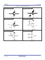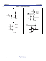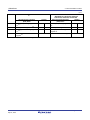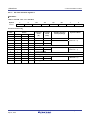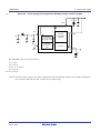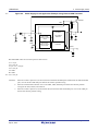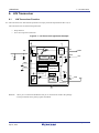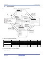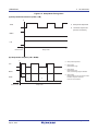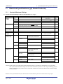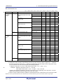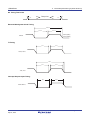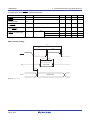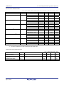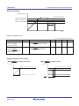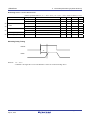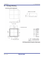
1
User’s Manual 8 μPD78F807x Microcontroller with LIN Transceiver & Half-Bridge Drivers User’s Manual: Hardware RENESAS MCU μPD78F807x Microcontroller μPD78F8071(A) μPD78F8072(A) μPD78F8073(A) μPD78F8074(A) μPD78F8075(A) μPD78F8077D All information contained in these materials, including products and product specifications, represents information on the product at the time of publication and is subject to change by Renesas Electronics Corp. without notice. www.renesas.com Rev.2.00 Sep 2012 Notice 1. Descriptions of circuits, software and other related information in this document are provided only to illustrate the operation of semiconductor products and application examples. You are fully responsible for the incorporation of these circuits, software, and information in the design of your equipment. Renesas Electronics assumes no responsibility for any losses incurred by you or third parties arising from the use of these circuits, software, or information. 2. Renesas Electronics has used reasonable care in preparing the information included in this document, but Renesas Electronics does not warrant that such information is error free. Renesas Electronics assumes no liability whatsoever for any damages incurred by you resulting from errors in or omissions from the information included herein. 3. Renesas Electronics does not assume any liability for infringement of patents, copyrights, or other intellectual property rights of third parties by or arising from the use of Renesas Electronics products or technical information described in this document. No license, express, implied or otherwise, is granted hereby under any patents, copyrights or other intellectual property rights of Renesas Electronics or others. 4. You should not alter, modify, copy, or otherwise misappropriate any Renesas Electronics product, whether in whole or in part. Renesas Electronics assumes no responsibility for any losses incurred by you or third parties arising from such alteration, modification, copy or otherwise misappropriation of Renesas Electronics product. 5. Renesas Electronics products are classified according to the following two quality grades: “Standard” and “High Quality”. The recommended applications for each Renesas Electronics product depends on the product’s quality grade, as indicated below. “Standard”: Computers; office equipment; communications equipment; test and measurement equipment; audio and visual equipment; home electronic appliances; machine tools; personal electronic equipment; and industrial robots etc. “High Quality”: Transportation equipment (automobiles, trains, ships, etc.); traffic control systems; anti-disaster systems; anticrime systems; and safety equipment etc. Renesas Electronics products are neither intended nor authorized for use in products or systems that may pose a direct threat to human life or bodily injury (artificial life support devices or systems, surgical implantations etc.), or may cause serious property damages (nuclear reactor control systems, military equipment etc.). You must check the quality grade of each Renesas Electronics product before using it in a particular application. You may not use any Renesas Electronics product for any application for which it is not intended. Renesas Electronics shall not be in any way liable for any damages or losses incurred by you or third parties arising from the use of any Renesas Electronics product for which the product is not intended by Renesas Electronics. 6. You should use the Renesas Electronics products described in this document within the range specified by Renesas Electronics, especially with respect to the maximum rating, operating supply voltage range, movement power voltage range, heat radiation characteristics, installation and other product characteristics. Renesas Electronics shall have no liability for malfunctions or damages arising out of the use of Renesas Electronics products beyond such specified ranges. 7. Although Renesas Electronics endeavors to improve the quality and reliability of its products, semiconductor products have specific characteristics such as the occurrence of failure at a certain rate and malfunctions under certain use conditions. Further, Renesas Electronics products are not subject to radiation resistance design. Please be sure to implement safety measures to guard them against the possibility of physical injury, and injury or damage caused by fire in the event of the failure of a Renesas Electronics product, such as safety design for hardware and software including but not limited to redundancy, fire control and malfunction prevention, appropriate treatment for aging degradation or any other appropriate measures. Because the evaluation of microcomputer software alone is very difficult, please evaluate the safety of the final products or systems manufactured by you. 8. Please contact a Renesas Electronics sales office for details as to environmental matters such as the environmental compatibility of each Renesas Electronics product. Please use Renesas Electronics products in compliance with all applicable laws and regulations that regulate the inclusion or use of controlled substances, including without limitation, the EU RoHS Directive. Renesas Electronics assumes no liability for damages or losses occurring as a result of your noncompliance with applicable laws and regulations. 9. Renesas Electronics products and technology may not be used for or incorporated into any products or systems whose manufacture, use, or sale is prohibited under any applicable domestic or foreign laws or regulations. You should not use Renesas Electronics products or technology described in this document for any purpose relating to military applications or use by the military, including but not limited to the development of weapons of mass destruction. When exporting the Renesas Electronics products or technology described in this document, you should comply with the applicable export control laws and regulations and follow the procedures required by such laws and regulations. 10. It is the responsibility of the buyer or distributor of Renesas Electronics products, who distributes, disposes of, or otherwise places the product with a third party, to notify such third party in advance of the contents and conditions set forth in this document, Renesas Electronics assumes no responsibility for any losses incurred by you or third parties as a result of unauthorized use of Renesas Electronics products. 11. This document may not be reproduced or duplicated in any form, in whole or in part, without prior written consent of Renesas Electronics. 12. Please contact a Renesas Electronics sales office if you have any questions regarding the information contained in this document or Renesas Electronics products, or if you have any other inquiries. (Note 1) “Renesas Electronics” as used in this document means Renesas Electronics Corporation and also includes its majorityowned subsidiaries. (Note 2) “Renesas Electronics product(s)” means any product developed or manufactured by or for Renesas Electronics. (2012.4) NOTES FOR CMOS DEVICES (1) VOLTAGE APPLICATION WAVEFORM AT INPUT PIN: Waveform distortion due to input noise or a reflected wave may cause malfunction. If the input of the CMOS device stays in the area between VIL (MAX) and VIH (MIN) due to noise, etc., the device may malfunction. Take care to prevent chattering noise from entering the device when the input level is fixed, and also in the transition period when the input level passes through the area between VIL (MAX) and VIH (MIN). (2) HANDLING OF UNUSED INPUT PINS: Unconnected CMOS device inputs can be cause of malfunction. If an input pin is unconnected, it is possible that an internal input level may be generated due to noise, etc., causing malfunction. CMOS devices behave differently than Bipolar or NMOS devices. Input levels of CMOS devices must be fixed high or low by using pull-up or pull-down circuitry. Each unused pin should be connected to VDD or GND via a resistor if there is a possibility that it will be an output pin. All handling related to unused pins must be judged separately for each device and according to related specifications governing the device. (3) PRECAUTION AGAINST ESD: A strong electric field, when exposed to a MOS device, can cause destruction of the gate oxide and ultimately degrade the device operation. Steps must be taken to stop generation of static electricity as much as possible, and quickly dissipate it when it has occurred. Environmental control must be adequate. When it is dry, a humidifier should be used. It is recommended to avoid using insulators that easily build up static electricity. Semiconductor devices must be stored and transported in an anti-static container, static shielding bag or conductive material. All test and measurement tools including work benches and floors should be grounded. The operator should be grounded using a wrist strap. Semiconductor devices must not be touched with bare hands. Similar precautions need to be taken for PW boards with mounted semiconductor devices. (4) STATUS BEFORE INITIALIZATION: Power-on does not necessarily define the initial status of a MOS device. Immediately after the power source is turned ON, devices with reset functions have not yet been initialized. Hence, power-on does not guarantee output pin levels, I/O settings or contents of registers. A device is not initialized until the reset signal is received. A reset operation must be executed immediately after power-on for devices with reset functions. (5) POWER ON/OFF SEQUENCE: In the case of a device that uses different power supplies for the internal operation and external interface, as a rule, switch on the external power supply after switching on the internal power supply. When switching the power supply off, as a rule, switch off the external power supply and then the internal power supply. Use of the reverse power on/off sequences may result in the application of an overvoltage to the internal elements of the device, causing malfunction and degradation of internal elements due to the passage of an abnormal current. The correct power on/off sequence must be judged separately for each device and according to related specifications governing the device. (6) INPUT OF SIGNAL DURING POWER OFF STATE : Do not input signals or an I/O pull-up power supply while the device is not powered. The current injection that results from input of such a signal or I/O pull-up power supply may cause malfunction and the abnormal current that passes in the device at this time may cause degradation of internal elements. Input of signals during the power off state must be judged separately for each device and according to related specifications governing the device. How to Use This Manual Readers This manual is intended for user engineers who wish to understand the functions of the μ PD78F807x, and to design and develop application systems and programs for this device. Purpose This manual is intended to give users an understanding of the functions described in the Organization below. Organization There are four manuals for the μ PD78F807x microcontroller: this manual, 78K0/Kx2 User’s Manual, 78K0/Kx2 ROM Expansion Products User’s Manual, and the Instructions edition (common to the 78K0 Series). μ PD78F807x 78K0/Kx2 78K0/Kx2 Microcontroller User’s Manual ROM Expansion Products User’s Manual User’s Manual • Pin functions • Pin functions • CPU architecture • Internal block functions • Internal block functions • Memory bank switching • On-chip peripheral • Interrupts functions • Other on-chip peripheral • Multiplier/divider functions • Flash memory • Electrical specifications • function Electrical specifications 78K/0 Series User’s Manual Instructions • CPU functions • Instruction set • Explanation of each instruction How to Read This Manual It is assumed that the readers of this manual have general knowledge of electrical engineering, logic circuits, and microcontrollers. • To gain a general understanding of functions: → Read this manual in the order of the CONTENTS. The mark “<R>” shows major revised points. The revised points can be easily searched by copying an “<R>” in the PDF file and specifying it in the “Find what:” field. • The notation of the product name → Description of (A) is omitted in this manual. “(A)” product names should be read as follows. - μ PD78F8071 → μ PD78F8071(A) - μ PD78F8072 → μ PD78F8072(A) - μ PD78F8073 → μ PD78F8073(A) - μ PD78F8074 → μ PD78F8074(A) - μ PD78F8075 → μ PD78F8075(A) • To know details of the microcontroller block: → Refer to the separate documents: 78K0/Kx2 User’s Manual (R01UH0008) and 78K0/Kx2 ROM Expansion Products User’s Manual (U19719E). 78K0/KC2 Microcontroller Products Product Name corresponding to 78K0/KC2 Microcontroller Products μ PD78F0511A μ PD78F8071 μ PD78F0512A μ PD78F8072 μ PD78F0513A μ PD78F8073 μ PD78F0514A μ PD78F8074 μ PD78F0515A μ PD78F8075 μ PD78F0517DA μ PD78F8077D • To know details of the 78K0 microcontroller instructions: → Refer to the separate document: 78K/0 Series Instructions User’s Manual (U12326E). Conventions Data significance: Higher digits on the left and lower digits on the right Active low representations: ××× (overscore over pin and signal name) Note: Footnote for item marked with Note in the text Caution: Information requiring particular attention Remark: Supplementary information Numerical representations: Binary ... ×××× or ××××B Decimal ... ×××× Hexadecimal ... ××××H Related Documents The related documents indicated in this publication may include preliminary versions. However, preliminary versions are not marked as such. Documents Related to Devices Document Name μ PD78F807x Microcontroller with LIN Transceiver & Half-Bridge Drivers User’s Manual: Document No. This Manual Hardware 78K0/Kx2 User’s Manual R01UH0008 78K0/Kx2 ROM Expansion Products User’s Manual U19719E 78K/0 Microcontroller Instructions User’s Manual U12326E 78K0/Kx2 Flash Memory Programming (Programmer) Application Note U17739E 78K0 Microcontrollers Self Programming Library Type01 User’s Manual U18274E 78K0 Microcontrollers EEPROM TM Emulation Library Type01 User’s Manual U18275E Documents Related to Flash Memory Programming Document Name PG-FP5 Flash Memory Programmer User’s Manual Document No. R20UT0008 Other Documents Document Name Document No. RENESAS MICROCOMPUTER GENERAL CATALOG R01CS0001E Semiconductor Package Mount Manual Note Guide to Prevent Damage for Semiconductor Devices by Electrostatic Discharge (ESD) C11892E Review of Quality and Reliability Handbook Information C12769E Note See the “Semiconductor Package Mount Manual” website (http://www.renesas.com/products/package/manual/index.jsp) Caution The related documents listed above are subject to change without notice. Be sure to use the latest version of each document when designing. Caution: This product uses SuperFlash® technology licensed from Silicon Storage Technology, inc. EEPROM is a trademark of Renesas Electronics Corporation. SuperFlash is a registered trademark of Silicon Storage Technology, Inc. in several countries including the United States and Japan. CONTENTS 1. Outline ............................................................................................................................................. 1 1.1 Features ....................................................................................................................................... 1 1.2 Applications................................................................................................................................. 3 1.3 Ordering Information .................................................................................................................. 3 1.4 Pin Configuration (Top View)..................................................................................................... 4 1.5 Block Diagram ............................................................................................................................. 6 1.6 1.5.1 Microcontroller Block Diagram ......................................................................................................... 7 1.5.2 Analog Block Diagram ..................................................................................................................... 8 Outline of Functions ................................................................................................................... 9 2. Pin Functions ......................................................................................................................................... 11 2.1 Microcontroller Block Pin Functions ...................................................................................... 12 2.2 Analog Part Pins........................................................................................................................ 16 2.3 Description of Pin Functions ................................................................................................... 18 2.3.1 P00, P01 (Port 0) ........................................................................................................................... 18 2.3.2 P10 to P17 (Port 1) ........................................................................................................................ 19 2.3.3 P20 to P24 (Port 2) ........................................................................................................................ 20 2.3.4 P30 to P33 (port 3)......................................................................................................................... 21 2.3.5 P60 to P61 (port 6)......................................................................................................................... 22 2.3.6 P70 (port 7) .................................................................................................................................... 22 2.3.7 P120 to P122 (port 12)................................................................................................................... 24 2.3.8 P130 (port 13) ................................................................................................................................ 25 2.3.9 AVREF, AVSS, VDD, VSS .................................................................................................................... 25 2.3.10 RESET........................................................................................................................................... 25 2.3.11 REGC ............................................................................................................................................ 26 2.3.12 FLMD0 ........................................................................................................................................... 26 2.3.13 HBO1 to HBO 6 ............................................................................................................................. 26 2.3.14 SUP1 to SUP6 ............................................................................................................................... 26 2.3.15 GND, GND1 to GND6, GND_DRV................................................................................................. 26 2.3.16 RESET_A ...................................................................................................................................... 26 2.3.17 LIN ................................................................................................................................................. 27 2.3.18 MSLP ............................................................................................................................................. 27 2.3.19 MOD1, MOD2 ................................................................................................................................ 27 2.3.20 VRO ............................................................................................................................................... 27 2.3.21 VRS ............................................................................................................................................... 27 2.3.22 SVDD............................................................................................................................................. 27 2.3.23 SRC ............................................................................................................................................... 27 Index-1 2.3.24 SCKA ............................................................................................................................................. 28 2.3.25 SOA ............................................................................................................................................... 28 2.3.26 SIA ................................................................................................................................................. 28 2.3.27 SSA................................................................................................................................................ 28 2.3.28 PWMI ............................................................................................................................................. 28 2.3.29 INH................................................................................................................................................. 28 2.3.30 IC ................................................................................................................................................... 28 2.4 Pin I/O Circuits and Recommended Connection of Unused Pins........................................ 29 3. Microcontroller Functions .................................................................................................................... 35 3.1 Differences in Functions between μPD78F807x and 78K0/KC2 ........................................... 35 3.2 Differences in Special Function Registers between μPD78F807x and 78K0/KC2.............. 36 3.3 Differences in Register Bit Settings between μPD78F807x and 78K0/KC2......................... 38 3.3.1 Port mode register ......................................................................................................................... 38 3.3.2 Port register ................................................................................................................................... 39 3.3.3 Pull-up resistor option register ....................................................................................................... 39 3.3.4 Analog input channel specification register .................................................................................... 40 3.3.5 A/D port configuration register ....................................................................................................... 41 3.3.6 External interrupt rising/falling edge enable register ...................................................................... 42 3.3.7 Key return mode register ............................................................................................................... 43 3.3.8 Watch timer operation mode register ............................................................................................. 43 3.3.9 Clock operation mode select register............................................................................................. 44 3.3.10 Processor clock control register ..................................................................................................... 44 3.3.11 IIC clock selection register 0 .......................................................................................................... 45 3.3.12 Interrupt request flag register (IF1L) .............................................................................................. 47 3.3.13 Interrupt mask flag register (MK1L)................................................................................................ 47 3.3.14 Priority specification flag register (PR1L) ....................................................................................... 48 4. Writing with Flash Programmer ........................................................................................................... 49 5. Power Supply Circuit............................................................................................................................. 51 5.1 Power Supply Function ............................................................................................................ 51 5.2 Regulator Output Function ...................................................................................................... 51 5.3 External Sensor Power Supply Output Function................................................................... 51 5.4 Over Current Protection Function ........................................................................................... 51 5.5 Low-Voltage Detection Function ............................................................................................. 52 5.6 External Dropper Auxiliary Function....................................................................................... 52 6. LIN Transceiver...................................................................................................................................... 55 6.1 LIN Transceiver Function ......................................................................................................... 55 Index-2 6.2 Operation Modes ....................................................................................................................... 56 6.3 Over Current Limiter ................................................................................................................. 62 7. Half-Bridge Circuit ................................................................................................................................. 63 7.1 Half-Bridge Drivers.................................................................................................................... 63 7.2 Over Current Protection Function ........................................................................................... 65 7.3 Through-Current Protection Function .................................................................................... 65 8. SPI & PWM Controller ........................................................................................................................... 67 8.1 SPI & PWM Controller ............................................................................................................... 67 8.2 SPI Communication .................................................................................................................. 68 8.3 SPI Control Registers ............................................................................................................... 70 9. Protection Functions............................................................................................................................. 76 9.1 Thermal Shutdown Circuit Operation ..................................................................................... 77 9.2 Over Current Limiter Operation ............................................................................................... 78 9.2.1 Power Supply Circuit...................................................................................................................... 78 9.2.2 LIN Transceiver.............................................................................................................................. 78 9.2.3 Half-Bridge Circuit.......................................................................................................................... 78 10. Analog Reset Function ....................................................................................................................... 79 11. Electrical Specifications ((A) Grade Products)................................................................................. 81 11.1 Absolute Maximum Ratings ..................................................................................................... 81 11.2 Microcontroller Block Electrical Characteristics ................................................................... 83 11.3 Analog Block Characteristics ................................................................................................ 104 12. Package Drawing ............................................................................................................................... 113 APPENDEX A PACKAGE HEAT-DISSIPATION ................................................................................... 114 APPENDEX B CALCULATION EXAMPLE OF TOTAL POWER DISSIPATION AND JUNCTION TEMPERATURE ............................................................................................................. 115 APPENDEX C REVISION HISTORY ....................................................................................................... 116 C.1 Major Revisions in This Edition............................................................................................. 116 Index-3 μPD78F807x Microcontroller R01UH0281EJ0200 Rev.2.00 Sep 27, 2012 with LIN Transceiver & Half-Bridge Drivers 1. Outline μPD78F807x is an MCP (Multi-Chip Package) which includes 2 chips in 1 package: an analog chip (incorporating the LIN transceiver, power supply, six-channel half-bridge drivers) and an 8-bit microcontroller chip. The 78K0/KC2 is used in the 8-bit microcontroller block of μPD78F807x. 1.1 • ROM, RAM capacities Note • • • • • • • • Features ROM Note High-Speed RAM Note Expansion RAM Note Product (64 Pins) 16 KB 768 B - μPD78F8071 24 KB 1 KB - μPD78F8072 32 KB 1 KB - μPD78F8073 48 KB 1 KB 1 KB μPD78F8074 60 KB 1 KB 2 KB μPD78F8075 128 KB 1 KB 6 KB μPD78F8077D The internal flash memory, internal high-speed RAM capacities, and internal expansion RAM capacities can be changed using the internal memory size switching register (IMS) and the internal expansion RAM size switching register (IXS). On-chip single-power-supply flash memory Self-programming (with boot swap function) On-chip debug function (μPD78F8077D only) Note 1 On-chip power-on-clear (POC) circuit and low-voltage detector (LVI) On-chip watchdog timer (operable with the internal low speed oscillation clock) On-chip multiplier/divider Note 2 On-chip key interrupt function I/O ports: μPD78F807x: 26 (N-ch open drain: 2) Notes 1. The μPD78F8077D has an on-chip debug function, which is provided for development and evaluation. Do not use the on-chip debug function in products designated for mass production, because the guaranteed number of rewritable times of the flash memory may be exceeded when this function is used, and product reliability therefore cannot be guaranteed. Renesas Electronics is not liable for problems occurring when the on-chip debug function is used. 2. Only supported by the product with 48-Kbyte or more flash memory. R01UH0281EJ0200 Rev.2.00 Sep 27, 2012 Page 1 of 117 μPD78F807x • • <R> • • <R> • • <R> • • • 1. Outline Timer: 7 channels ⎯ 16-bit timer/event counter: 1 channel ⎯ 8-bit timer/event counter: 2 channels ⎯ 8-bit timer: 2 channels ⎯ Watch timer: 1 channel ⎯ Watch dog timer: 1 channel Serial interface: 3 channels ⎯ UART (LIN (Local Interconnect Network)-bus supported): 1 channel ⎯ CSI/UART Note : 1 channel ⎯ IIC: 1 channel 10-bit resolution A/D converter: 5 channels On-chip power supply circuit Output voltage: 5 V ± 3% On-chip power supply output function for external sensors On-chip external dropper auxiliary function On-chip over current limiter LIN transceiver The LIN transceiver complies with LIN Specifications Rev.2.0, 2.1 Low power consumption achieved with on-chip sleep function On-chip pull-up resistors for slave applications On-chip over current limiter Driver Half-bridge driver: 6 channels On-chip over current limiter Overheat protection circuit SPI & PWM controller:1 channel Package: 64-pin plastic WQFN (fine-pitch) (9x9) Operation ambient temperature: (A) grade products: TA = -40 to +85 °C Note Select either of these functions since they share the same pins. R01UH0281EJ0200 Rev.2.00 Sep 27, 2012 Page 2 of 117 μPD78F807x 1.2 • 1. Outline Applications Automotive equipment System control for body electronic control units ⎯ Mirror control ⎯ Flap control, etc. 1.3 Ordering Information Part Number μPD78F8071K8A-6B4-G Package Quality Grade Note 64-pin plastic WQFN (fine pitch) (9×9) Special (for high-reliability electronics equipment) μPD78F8072K8A-6B4-G Note 64-pin plastic WQFN (fine pitch) (9×9) Special (for high-reliability electronics equipment) μPD78F8073K8A-6B4-G Note 64-pin plastic WQFN (fine pitch) (9×9) Special (for high-reliability electronics equipment) μPD78F8074K8A-6B4-G Note 64-pin plastic WQFN (fine pitch) (9×9) Special (for high-reliability electronics equipment) μPD78F8075K8A-6B4-G Note 64-pin plastic WQFN (fine pitch) (9×9) Special (for high-reliability electronics equipment) μPD78F8077DK8-6B4-G 64-pin plastic WQFN (fine pitch) (9×9) Standard (for general electronics equipment) Note (A) grade product R01UH0281EJ0200 Rev.2.00 Sep 27, 2012 Page 3 of 117 μPD78F807x 1.4 1. Outline Pin Configuration (Top View) VRO VRS GND LIN GND_DRV MOD1 MOD2 SRC RESET_A AVREF AVSS P24/ANI4 P23/ANI3 P22/ANI2 P21/ANI1 P20/ANI0 <R> 64-pin plastic WQFN (fine-pitch) (9×9) 64 63 62 61 60 59 58 57 56 55 54 53 52 51 50 49 1 48 SVDD 2 47 P30/INTP1 P00/TI000 3 46 SUP P120/INTP0/EXLVI 4 45 IC RESET 5 44 GND6 FLMD0 6 43 HBO6 7 42 SUP6 8 41 SUP5 9 40 HBO5 VSS 10 39 GND5 P130 P01/TI010/TO00 P122/X2/EXCLK(/OCD0B Note P121/X1(/OCD0A Note ) ) REGC VDD 11 38 GND4 P60/SCL0 12 37 HBO4 P61/SDA0 13 36 SUP4 14 35 SUP3 15 34 HBO3 16 33 GND3 P33/TI51/TO51/INTP4 P70/KR0 P32/INTP3(/OCD1B Note ) Note GND2 HBO2 SUP2 SUP1 HBO1 GND1 P10/SCK10/TxD0/SCKA P11/SI10/RxD0/SOA P12/SO10/SIA P13/TxD6/TxL P14/RxD6/RxL P15/TOH0/PWMI P16/TOH1/INTP5/SSA P17/TI50/TO50/INH MSLP P31/INTP2(/OCD1ANote) 17 18 19 20 21 22 23 24 25 26 27 28 29 30 31 32 μPD78F8077D (with on-chip debug function) only Cautions 1. Make GND, GND1 to GND6, and GND_DRV the same potential as VSS and AVSS. 2. Connect the REGC pin to VSS via a capacitor (0.47 μF to 1 μF). 3. ANI0/P20 to ANI4/P24 are in the analog input mode after reset release. <R> 4. Make SUP the same potential as SUP1 to SUP6. <R> 5. Make VDD the same potential as VRS or VRO when the on-chip P-ch MOS is used for the 5-V output dropper. 6. Make VDD the same potential as VRS when the external dropper is used for the 5-V output dropper. <R> R01UH0281EJ0200 Rev.2.00 Sep 27, 2012 Page 4 of 117 μPD78F807x 1. Outline <R> Pin Identification ANI0 to ANI4 AVREF AVSS EXCLK EXLVI FLMD0 GND GND1 to GND6 GND_DRV HBO1 to HBO6 IC INTP0 to INTP5 KR0 LIN MOD1, MOD2 MSLP OCD0A, OCD0B, OCD1A, OCD1B P00, P01 P10 to P17 P20 to P24 P30 to P33 P60, P61 P70 P120 to P122 P130 REGC RESET : Analog Input : Analog Reference Voltage : Analog Ground : External Clock Input (Main System Clock) : External potential Input for Low-voltage detector : Flash Programming Mode : Ground : Half-bridge Driver Output : Internal Connection : External Interrupt Input : Key Return : LIN Bus : Pin Mode Control Input : Sleep Mode Control Input : On-Chip Debug Input/Output : Port 0 : Port 1 : Port 2 : Port 3 : Port 6 : Port 7 : Port 12 : Port 130 : Regulator Capacitance : Reset R01UH0281EJ0200 Rev.2.00 Sep 27, 2012 RxD0, RxD6 SCK10, SCL0 SDA0 SI10 SO10 SRC SUP SUP1 to SUP6 SCKA SIA SOA SSA PWMI TI000 TI010, TI50, TI51 TO00, TO01, TO50, TO51, TOH0, TOH1 TxD0, TxD6 INH VDD VRO VRS SVDD External RESET_A VSS X1, X2 : Receive Data : Serial Clock Input/Output : Serial Data Input/Output : Serial Data Input : Serial Data Output : Slew Rate Control Input : Battery Power Supply : Serial Clock Input : Serial Data Input : Serial Data Output : Slave Select Input : PWM Input : Timer Input : Timer Output : Transmit Data : Inhibit Input for Half-bridge Driver Enable : Power Supply : Voltage Regulator Output : Voltage Regulator Input : Voltage Regulator Output for Sensor device : Analog chip Reset : Ground : Crystal Oscillator (Main System Clock) Page 5 of 117 μPD78F807x <R> 1.5 1. Outline Block Diagram P16/TOH1/INTP5/SSA P15/TOH0/PWMI P12/SO10/SIA P11/SI10/SOA P10/SCK10/SCKA SUP Analog chip 8-bit Micro. (78K0/KC2, 48pin) Voltage Regulator •Flash ROM: 16KB/24KB/32KB/ 48KB/60KB/128KB •Expansion RAM: 1KB/2KB/6KB •High -Speed RAM: 768B/1KB VRS VRO SVDD MSLP LIN transceiver LIN SRC P16/TOH1/INTP5 SSA SPI & PWM control SOA P15/TOH0 P12/SO10 P11/SI10 SCKA P10/SCK10 PWMI SIA SUP1 to 6 HBO1 to 6 GND1 to 6 MOD1 VDD AVREF REGC RESET FLMD0 P00/TI000 P01/TI010/TO00 P20/ANI0 to P24/ANI4 P30/INTP1 Note P31/INTP2 (/OCD1A ) Note P32/INTP3 (/OCD1B ) P33/TI51/TO51/INTP4 P60/SCL0 P61/SDA0 P70/KR0 P120/INTP0/EXLVI Note P121/X1(/OCD0A ) Note P122/X2/EXCLK (/OCD0B ) P130 Half bridge Driver INH P17/TI50/TO50 TxL P13/TxD6 RxL P14/RxD6 Mode control MOD2 Reset_A Reset control GND Note GND_DRV P14/RxD6/RxL P13/TxD6/TxL P17/TI50/TO50/INH VSS AVSS μPD78F8077D (with on-chip debug function) only Cautions 1. μPD78F807x is developed as an MCP (Multi-Chip Package) which includes two chips in the package, a microcontroller chip and an analog chip (power supply circuit, LIN transceiver, and half-bridge circuit). 2. The P10/SCK10/SCKA, P11/SI10/SOA, P12/SO10/SIA, P13/TxD6/TxL, P14/RxD6/RxL, P15/TOH0/PWMI, P16/TOH1/INTP5/SSA, and P17/TI50/TO50/INH pins are connected inside the package. R01UH0281EJ0200 Rev.2.00 Sep 27, 2012 Page 6 of 117 μPD78F807x <R> 1.5.1 1. Outline Microcontroller Block Diagram TO00/TI010/P01 16-bit TIMER/ EVENT COUNTER 00 TI000/P00 RxD6/P14(LINSEL) TOH0/P15 8-bit TIMER H0 TOH1/P16 8-bit TIMER H1 Low-SPEED INTERNAL OSCILLATOR WATCHDOG TIMER PORT0 2 P00, P01 PORT1 8 P10 to P17 PORT2 5 P20 to P24 PORT3 4 P30 to P33 PORT6 2 P60, P61 P70 PORT7 78K/0 CPU CORE FLASH MEMORY PORT12 3 P130 PORT13 8-bit TIMER/ EVENT COUNTER 50 TI50/TO50/P17 POWER ON CLEAR/ LOW VOLTAGE INDICATOR 8-bit TIMER/ EVENT COUNTER 51 TI51/TO51/P33 WATCH TIMER INTERNAL HIGH-SPEED RAM INTERNAL EXPANSION Note1 RAM SERIAL INTERFACE UART0 RxD0/P11 TxD0/P10 TxD6/P13 LINSEL SI10/P11 KEY RETURN SCK10/P10 EXLVI/P120 KR0/P70 RESET CONTROL Note2 Note2 OCD0A /X1, OCD1A /P31 Note2 Note2 OCD0B /X2, OCD1B /P32 ON-CHIP DEBUGNote2 RxD6/P14(LINSEL) SERIAL INTERFACE CSI10 SO10/P12 POC/LVI CONTROL MULTIPLIER& DIVIDERNote1 SERIAL INTERFACE UART6 RxD6/P14 P120 to P122 INTERRUPT CONTROL INTP0/P120 4 INTP1/P30 to INTP4/P33 INTP5/P16 SERIAL INTERFACE IIC0 SDA0/P61 SCL0/P60 ANI0/P20 to ANI4/P24 AVREF SYSTEM CONTROL X1/P121 X2/EXCLK/P122 HIGH-SPEED INTERNAL OSCILLATOR 5 A/D CONVERTER AVSS RESET VDD VSS FLMD0 VOLTAGE REGULATOR REGC Notes 1. Only supported by the products with 48-Kbyte or more flash memory. 2. μPD78F8077D (with on-chip debug function) only. R01UH0281EJ0200 Rev.2.00 Sep 27, 2012 Page 7 of 117 μPD78F807x <R> 1.5.2 1. Outline Analog Block Diagram SCKA Over current Limiter SIA Low-voltage detector SUP VRS SOA SPI & PWM controller Power supply circuit SSA PWMI SVDD VRO RESET_A GND Reset cirauit LIN pull-up resistor for slave Over current limiter RxL MSLP MOD1 LIN Slew rate selection circuit Mode control circuit Negative voltage input protection LIN transceiver MOD2 Thermal shutdown circuit SRC GND_DRV Half- bridge driver: 6 channels Ron (max.): 1Ω@1.5 A SUP1 to SUP6 Over current detector HBO1 to HBO6 Through-current protection circuit Half-bridge circuit R01UH0281EJ0200 Rev.2.00 Sep 27, 2012 TxL GND1 to GND6 INH Page 8 of 117 μPD78F807x 1.6 1. Outline Outline of Functions (1/2) Item Flash memory (KB) High-Speed RAM µPD78F8071 µPD78F8072 µPD78F8073 µPD78F8074 µPD78F8075 µPD78F8077D 16 24 32 48 60 128 2 6 768 bytes Expansion RAM (KB) 1 Kbyte - 1 Bank (flash memory) - Power supply voltage Regulator Included Minimum instruction execution time Clock 6 VDD = 1.8 to 5.5 V Main High-speed 0.1 μs (20 MHz: VDD = 2.7 to 5.5 V/0.4 μs (5 MHz: VDD = 1.8 to 5.5 V) 20 MHz: VDD = 2.7 to 5.5 V/5 MHz: VDD = 1.8 to 5.5 V system 8 MHz (TYP.): VDD = 1.8 to 5.5 V Internal highspeed oscillation Internal low-speed 240 kHz (TYP.): VDD = 1.8 to 5.5 V oscillation Port Timer Total 26 ch N-ch O.D. (6 V tolerance) 2 ch 16 bits (TM0) 1 ch 8 bits (TM5) 2 ch 8 bits (TMH) 2 ch Watch 1 ch WDT Serial UART/3-wire CSI interface 1 ch Note 1 ch UART supporting LIN-bus 1 ch 2 I C bus <R> 1 ch 10-bit A/D Interrupt 5 ch External 7 Internal 16 Key interrupt Reset RESET pin Provided POC LVI 1.59 V±0.15 V The detection level of the supply voltage is selectable. WDT Multiplier/divider On-chip debug function Provided Not provided Provided Not provided Operation ambient temperature Note Provided TA = -40 to +85 °C Select either of these functions since they share the same pins. R01UH0281EJ0200 Rev.2.00 Sep 27, 2012 Page 9 of 117 μPD78F807x 1. Outline (2/2) <R> Item µPD78F8071 µPD78F8072 µPD78F8073 µPD78F8074 µPD78F8075 µPD78F8077D • Includes P-ch MOS for dropper Power Supply - Output voltage: 5 V ± 3% (operating voltage range: 6 to 19 V, output current: 50 mA or less) • On-chip external-dropper (NPN transistor) auxiliary function - Output voltage: 5 V ± 3% (operating voltage range: 7 to 19 V, output current: 150 mA or less) • On-chip power supply output function for external sensors • On-chip over current protection circuit • Low-voltage detector • Complies with LIN Specifications Rev.2.0, 2.1 LIN transceiver • Sleep function supported • On-chip slew rate select function • On-chip pull-up resistors for slave applications • On-chip LIN driver current protection circuit • Half-bridge driver: 6 channels Driver • On-chip over current limiter • On-chip through-current protection circuit SPI & PWM controller 1 ch Overheat protection circuit 1 ch An outline of the timer is shown below. Function 16-Bit Timer/ 8-Bit Timer/ 8-Bit Timers Watch Watchdog Event Counter Event Counters H0 and H1 Timer Timer 00 50 and 51 TM00 TM50 TM51 TMH0 TMH1 Interval timer 1 channel 1 channel 1 channel 1 channel 1 channel - - External event 1 channel 1 channel 1 channel - - - - PPG output 1 output - - - - - - PWM output - 1 output 1 output 1 output 1 output - - Pulse width 2 input - - - - - - 1 output 1 output 1 output 1 output 1 output - - Carrier generator - - - - 1 outputNote - - Watch Timer - - - - - - - Watchdog timer - - - - - - 1 channel 2 1 1 1 1 - - counter measurement Square-wave output Interrupt source Note TM51 and TMH1 can be used in combination as a carrier generator mode. R01UH0281EJ0200 Rev.2.00 Sep 27, 2012 Page 10 of 117 μPD78F807x 2 Pin Functions 2. Pin Functions The differences in microcontroller pin functions between the μPD78F807x and 78K0/KC2 are as follows. <R> (1) Port and alternate function pins μPD78F807x 78K0/KC2 μPD78F0511A, 78F0512A, 78F0513A, 78F0514A, 78F0515A, 78F0517DA Pin name Alternate function Pin name Alternate function P10 SCK10/TxD0/SCKA P10 SCK10/TxD0 P11 SI10/RxD0/SOA P11 SI10/RxD0 P12 SO10/SIA P12 SO10 P13 TxD6/TxL P13 TxD6 P14 RxD6/RxL P14 RxD6 P15 TOH0/PWMI P15 TOH0 P16 TOH1/INTP5/SSA P16 TOH1/INTP5 P17 TI50/TO50/INH P17 TI50/TO50 P20 to P24 ANI0 to ANI4 P20 to P27 ANI0 to ANI7 - - P40 to P41 - - - P62 EXSCL0 - - P63 - P70 KR0 P70 to P73 KR0 to KR3 - - P74, P75 - - - P123 XT1 - - P124 XT2/EXCLKS - - P140 PCL/INTP6 R01UH0281EJ0200 Rev.2.00 Sep 27, 2012 Page 11 of 117 μPD78F807x 2.1 2 Pin Functions Microcontroller Block Pin Functions There are two types of pin I/O buffer power supplies: AVREF, and VDD. The relationship between these power supplies and the pins are shown below. <R> Table 2-1. Pin I/O Buffer Power Supplies Power Supply Corresponding Pins AVREF P20 to P24 VDD Pins other than P20 to P24 (1) Port pins (1/2) Function Name I/O P00 I/O P01 P10 I/O P11 P12 P13 Function After Reset Alternate Function Port 0. 2-bit I/O port. Input/output can be specified in 1-bit units. Use of an on-chip pull-up resistor can be specified by software setting. Input port TI000 Port 1. 8-bit I/O port. Input/output can be specified in 1-bit units. Use of an on-chip pull-up resistor can be specified by software setting. Input port SCK10/TxD0/SCKANote1 TI010/TO00 SI10/RxD0/SOA Note1 SO10/SIA Note1 TxD6/TxL Note1 P14 RxD6/RxL Note1 P15 TOH0/PWMI Note1 P16 TOH1/INTP5/SSA Note1 P17 TI50/TO50/INH <R> P20 to P24 I/O Port 2. 5-bit I/O port. Input/output can be specified in 1-bit units. Analog input ANI0 to ANI4 <R> P30 I/O Port 3. 4-bit I/O port. Input/output can be specified in 1-bit units. Use of an on-chip pull-up resistor can be specified by software setting. Input port INTP1 P31 P32 P33 Notes Note1 INTP2/OCD1A Note2 INTP3/OCD1B Note2 INTP4/TI51/TO51 1. Analog pin functions. This pin is connected to a function pin of the analog part inside the package. 2. μPD78F8077D only. R01UH0281EJ0200 Rev.2.00 Sep 27, 2012 Page 12 of 117 μPD78F807x 2 Pin Functions (1) Port pins (2/2) Function Name P60 I/O I/O P61 Function After Reset Port 6. 2-bit I/O port (N-ch open-drain). Input/output can be specified in 1-bit units. Input port Alternate Function SCL0 SDA0 P70 I/O Port 7. 1-bit I/O port. Input/output can be specified in 1-bit units. Use of an on-chip pull-up resistor can be specified by software setting. Input port KR0 P120 I/O Port 12. 3-bit I/O port. Input/output can be specified in 1-bit units. Only for P120, use of an on-chip pull-up resistor can be specified by software setting. Input port INTP0/EXLVI Port 13. 1-bit output only port. Output port P121 P122 <R> P130 Note Output X1/OCD0A Note X2/EXCLK/OCD0B Note - μPD78F8077D only. R01UH0281EJ0200 Rev.2.00 Sep 27, 2012 Page 13 of 117 μPD78F807x 2 Pin Functions (2) Non-port functions (1/2) Function Name <R> <R> <R> I/O Function After Reset ANI0 to ANI4 Input A/D converter analog input EXLVI Input Potential input for external low-voltage detection Input port P120/INTP0 FLMD0 - Flash memory programming mode setting - - INTP0 Input External interrupt request input for which the valid edge (rising edge, falling edge, or both rising and falling edges) can be specified Input port P120/EXLVI INTP1 Analog input Alternate Function P20 to P24 P30 INTP2 P31/OCD1A Note2 INTP3 P32/OCD1B Note2 INTP4 P33/TI51/TO51 INTP5 P16/TOH1/SSA Note1 KR0 Input Key interrupt input Input port P70 REGC - Connecting regulator output (2.5 V) stabilization capacitance for internal operation. Connect to VSS via a capacitor (0.47 to 1 μF). - - RESET Input System reset input - - RxD0 Input Serial data input to UART0 Input port P11/SI10/SOA RxD6 Input Serial data input to UART6 Input port P14/RxL SCK10 I/O Clock input/output for CSI10 Input port P10/TxD0/SCKA SI10 Input Serial data input from CSI10 Input port P11/RxD0/SOA SO10 Output Serial data output from CSI10 Input port P12 SCL0 I/O Clock input/output for IIC Input port P60 SDA0 I/O Serial data I/O for IIC Input port P61 TI000 Input External count clock input to 16-bit timer/event counter 00 Capture trigger input to capture registers (CR000, CR010) of 16-bit timer/event counter 00 Input port P00 TI010 TI50 Capture trigger input to capture register (CR000) of 16-bit timer/event counter 00 Input TI51 External count clock input to 8-bit timer/event counter 50 Note1 Note1 Note1 Note1 P01/TO00 Input port External count clock input to 8-bit timer/event counter 51 P17/TO50/INH Note1 P33/TO51/INTP4 TO00 Output 16-bit timer/event counter 00 output Input port P01/TI010 TO50 Output 8-bit timer/event counter 50 output Input port P17/TI50/INH Note1 TO51 8-bit timer/event counter 51 output P33/TI51/INTP4 TOH0 8-bit timer H0 output P15/PWMI TOH1 8-bit timer H1 output P16/INTP5/SSA Note1 Note1 TxD0 Output Serial data output from UART0 Input port P10/SCK10/SCKA TxD6 Output Serial data output from UART6 Input port P13/TxL Note1 Note1 Notes 1. Analog pin functions. This pin is connected to a function pin of the analog part inside the package. 2. μPD78F8077D only. R01UH0281EJ0200 Rev.2.00 Sep 27, 2012 Page 14 of 117 μPD78F807x 2 Pin Functions (2) Non-port functions (2/2) Function Name I/O X1 - X2 - Function Main system clock resonator connection After Reset Input port Alternate Function P121/OCD0A Note P122/EXCLK/ OCD0B Note EXCLK Input External clock input for main system clock Input port P122/X2 VDD - Positive power supply for pins other than P20 to P24 - - AVREF - A/D converter reference voltage input and positive power supply for P20 to P24 and A/D converter - - VSS - Ground potential for pins other than P20 to P24 - - AVSS - A/D converter ground potential. Make the same potential as VSS. - - Note: μPD78F8077D only. R01UH0281EJ0200 Rev.2.00 Sep 27, 2012 Page 15 of 117 μPD78F807x 2.2 2 Pin Functions Analog Part Pins (1/2) Function Name SSA Note PWMI Note I/O Function Input Slave select input Input External PWM input RxL Note Output Serial data output TxL Note Input Serial data input SIA Note Input Serial data input SOA Note Output Serial data output SCKA Note Input Clock input GND1 - Ground potential for half-bridge channel 1 HBO1 Output Output for half-bridge channel 1 SUP1 - Power supply for half-bridge channel 1 GND2 - Ground potential for half-bridge channel 2 HBO2 Output Output for half-bridge channel 2 SUP2 - Power supply for half-bridge channel 2 GND3 - Ground potential for half-bridge channel 3 HBO3 Output Output for half-bridge channel 3 SUP3 - Power supply for half-bridge channel 3 GND4 - Ground potential for half-bridge channel 4 HBO4 Output Output for half-bridge channel 4 SUP4 - Power supply for half-bridge channel 4 GND5 - Ground potential for half-bridge channel 5 HBO5 Output Output for half-bridge channel 5 SUP5 - Power supply for half-bridge channel 5 GND6 - Ground potential for half-bridge channel 6 HBO6 Output Output for half-bridge channel 6 SUP6 - Power supply for half-bridge channel 6 Note This pin is connected to the microcontroller pin functions inside the package. Cautions 1. Make GND, GND1 to GND6, and GND_DRV the same potential as VSS and AVSS. 2. Make SUP1 to SUP6 the same potential as SUP. R01UH0281EJ0200 Rev.2.00 Sep 27, 2012 Page 16 of 117 μPD78F807x 2 Pin Functions (2/2) Function Name <R> I/O Function SUP - Power supply connection SVDD Output Power supply output for external sensors VRO Output Power supply output or base control output for using external NPN transistor VRS Input Power supply and power-supply voltage monitor GND - Power supply circuit GND potential LIN I/O LIN Bus connection pin GND_DRV - LIN transceiver circuit GND MOD1, MOD2 Input Pin mode control input MSLP Input Sleep mode selection SRC Input Slew rate control input RESET_A Input Reset input to the analog chip side Note Input Half-bridge output-disable input INH Note This pin is connected to the microcontroller pin functions inside the package Cautions 1. Make GND, GND1 to GND6, and GND_DRV the same potential as VSS and AVSS. 2. Make SUP1 to SUP6 the same potential as SUP. <R> 3. Make VDD the same potential as VRS or VRO when the on-chip P-ch MOS is used for the 5-V output dropper. 4. Make VDD the same potential as VRS when the external dropper is used for the 5-V output dropper. <R> R01UH0281EJ0200 Rev.2.00 Sep 27, 2012 Page 17 of 117 μPD78F807x 2.3 Description of Pin Functions 2.3.1 P00, P01 (Port 0) 2 Pin Functions P00 and P01 are a 2-bit I/O port. These pins also function as timer I/O. The following operation modes can be specified in 1-bit units. (1) Port mode P00 and P01 function as a 2-bit I/O port. These pins can be set to input or output port in 1-bit units using port mode register 0 (PM0). An on-chip pull-up resistor can be used by setting the pull-up resistor option register 0 (PU0). (2) Control mode P00 and P01 function as timer I/O pins. (a) TI000 Functions as the external count clock input pin to 16-bit timer/event counter 00 and capture trigger signal input pin to the capture registers (CR000, CR010) of 16-bit timer/event counter 00. (b) TI010 Functions as the capture trigger signal input pin to the capture register (CR000) of 16-bit timer/event counters 00 and 01. (c) TO00 Functions as the timer output pin for 16-bit timer/event counter 00. R01UH0281EJ0200 Rev.2.00 Sep 27, 2012 Page 18 of 117 μPD78F807x 2.3.2 2 Pin Functions P10 to P17 (Port 1) P10 to P17 are an 8-bit I/O port. These pins also function as external interrupt request input, serial interface data I/O, clock I/O, and timer I/O pins. The following operation modes can be specified in 1-bit units. (1) Port mode P10 to P17 function as an 8-bit I/O port. These pins can be set to input or output port in 1-bit units using port mode register 1 (PM1). An on-chip pull-up resistor can be used by setting the pull-up resistor option register 1 (PU1). (2) Control mode P10 to P17 function as the external interrupt request input, serial interface data I/O, clock I/O, and timer I/O pins. (a) SI10 Functions as the serial data input pin for the serial interface CSI10. (b) SO10 Functions as the serial data output pin for the serial interface CSI10. (c) SCK10 Functions as the serial clock I/O pin for the serial interface CSI10. (d) RxD0 Functions as the serial data input pin for the serial interface UART0. (e) RxD6 Functions as the serial data input pin for the serial interface UART6. (f) TxD0 Functions as the serial data output pin for the serial interface UART0. (g) TxD6 Functions as the serial data output pin for the serial interface UART6. R01UH0281EJ0200 Rev.2.00 Sep 27, 2012 Page 19 of 117 μPD78F807x (h) 2 Pin Functions TI50 Functions as the external count clock input pin for the 8-bit timer/event counter 50. (i) TO50 Functions as the timer output pin for the 8-bit timer/event counter 50. (j) TOH0, TOH1 Function as the timer output pins for the 8-bit timers H0 and H1. (k) INTP5 Functions as the external interrupt request input pin for which the valid edge (rising edge, falling edge, or both rising and falling edges) can be specified. <R> 2.3.3 P20 to P24 (Port 2) P20 to P24 are an 5-bit I/O port. These pins also function as A/D converter analog input pins. The following operation modes can be specified in 1-bit units. (1) Port mode P20 to P24 function as an 5-bit I/O port. These pins can be set to input or output port in 1-bit units using port mode register 2 (PM2). (2) Control mode P20 to P24 function as the A/D converter analog input pins (ANI0 to ANI4). When using these pins as analog input pins, see 13.6 Cautions for A/D Converter in 78K0/Kx2 User’s Manual (R01UH0008E). (a) ANI0 to ANI4 Functions as the A/D converter analog input pins. Caution ANI0/P20 to ANI4/P24 are set to analog input mode after a reset is released. R01UH0281EJ0200 Rev.2.00 Sep 27, 2012 Page 20 of 117 μPD78F807x 2.3.4 2 Pin Functions P30 to P33 (port 3) P30 to P33 are a 4-bit I/O port. These pins also function as external interrupt request input and timer I/O pins. The following operation modes can be specified in 1-bit units. (1) Port mode P30 to P33 function as a 4-bit I/O port. These pins can be set to input or output port in 1-bit units using port mode register 3 (PM3). An on-chip pull-up resistor can be used by setting the pull-up resistor option register 3 (PU3). (2) Control mode P30 to P33 function as the external interrupt request input and timer I/O pins. (a) INTP1 to INTP4 Function as the external interrupt request input pins for which the valid edge (rising edge, falling edge, or both rising and falling edges) can be specified. (b) TI51 Functions as the external count clock input pin to 8-bit timer/event counter 51. (c) TO51 Functions as the timer output pin from 8-bit timer/event counter 51. Cautions 1. In μPD78F8077D (a product with the on-chip debug function), be sure to pull down the P31/INTP2/OCD1A pin before reset release to prevent malfunction. 2. When the flash memory programmer or on-chip debug emulator is connected but the P31/INTP2/OCD1 pin in a product with the on-chip debug function (μPD78F8077D) is not used, this pin should be handled as follows: P31/INTP2/OCD1A Flash memory programmer connected On-chip debug emulator connected (when P31/INTP2/OCD1A is not used as on-chip debug mode setting pin) Remarks Connect to VSS via a resistor. During reset When a reset is released Input: Connect to VDD or VSS via a resistor. Output: Leave open. In μPD78F8077D (a product with the on-chip debug function), P31 and P32 can be used as on-chip debug mode setting pins (OCD1A, OCD1B) when the on-chip debug function is used. For the connection to the in-circuit emulator supporting on-chip debugging (QB-78K0MINI), see CHAPTER 28 ON-CHIP DEBUG FUNCTION in 78K0/Kx2 User’s Manual (R01UH0008E). R01UH0281EJ0200 Rev.2.00 Sep 27, 2012 Page 21 of 117 μPD78F807x 2.3.5 2 Pin Functions P60 to P61 (port 6) P60 and P61 are a 2-bit I/O port. These pins also function as serial interface data I/O and clock I/O pins. The following operation modes can be specified in 1-bit units. (1) Port mode P60 and P61 function as a 2-bit I/O port. These pins can be set to input or output port in 1-bit units using port mode register 6 (PM6). Output of P60 and P61 is N-ch open-drain output (6 V tolerance). (2) Control mode P60 and P61 function as serial interface data I/O and clock I/O pins. (a) SDA0 Functions as the serial data I/O pin for the serial interface IIC0. (b) SCL0 Functions as the serial clock I/O pin for the serial interface IIC0. 2.3.6 P70 (port 7) P70 is a 1-bit I/O port. This pin also functions as a key interrupt input pin. The following operation modes can be specified. (1) Port mode P70 functions as a 1-bit I/O port. This pin can be set to input or output port using port mode register 7 (PM7). An onchip pull-up resistor can be used by setting the pull-up resistor option register 7 (PU7). (2) Control mode P70 functions as the key interrupt input pin. (a) KR0 Functions as the key interrupt input pin. R01UH0281EJ0200 Rev.2.00 Sep 27, 2012 Page 22 of 117 μPD78F807x 2.3.7 2 Pin Functions P120 to P122 (port 12) P120 to P122 are a 3-bit I/O port. These pins also function as external interrupt request input, external low-voltage detection potential input, main system clock resonator connection, and main system clock external clock input pins. The following operation modes can be specified in 1-bit units. (1) Port mode P120 to P122 function as a 3-bit I/O port. These pins can be set to input or output port using port mode register 12 (PM12). Only for P120, an on-chip pull-up resistor can be used by setting the pull-up resistor option register 12 (PU12). (2) Control mode P120 to P122 function as pins for the external interrupt request input, potential input for external low-voltage detection, connecting resonator for main system clock, and external clock input for main system clock. (a) INTP0 Functions as the external interrupt request input pin (INTP0) for which the valid edge (rising edge, falling edge, or both rising and falling edges) can be specified. (b) EXLVI Functions as the potential input pin for external low-voltage detection. (c) X1, X2 Function as the resonator connection pins for the main system clock. (d) EXCLK Functions as the external clock input pin for the main system clock. Caution When the flash memory programmer or on-chip debug emulator is connected but the P121/X1/OCD0A pin in a product with the on-chip debug function (μPD78F8077D) is not used, this pin should be handled as follows: P121/X1/OCD0A Flash memory programmer connected On-chip debug emulator connected (when P121/X1/OCD0A is not used as on-chip debug mode setting pin) R01UH0281EJ0200 Rev.2.00 Sep 27, 2012 Connect to VSS via a resistor. During reset When a reset is released Input: Connect to VDD or VSS via a resistor. Output: Leave open. Page 23 of 117 μPD78F807x In μPD78F8077D (a product with the on-chip debug function), P121 and P122 can be used as on-chip debug mode setting pins (OCD0A, OCD0B) when the on-chip debug function is used. For the connection to the in-circuit emulator supporting on-chip debugging (QB-78K0MINI), see CHAPTER 28 ON-CHIP DEBUG FUNCTION in 78K0/Kx2 User’s Manual (R01UH0008E). Remarks <R> 2.3.8 2 Pin Functions P130 (port 13) P130 functions as an output-only port. Remark When the device is reset, P130 outputs a low level. Therefore, to output a high level from P130 before the device is reset, the output signal of P130 can be used as a pseudo reset signal of the CPU (see the figure for Remark in 5.2.10 Port 13 in 78K0/Kx2 User’s Manual (R01UH0008E)). 2.3.9 (a) AVREF, AVSS, VDD, VSS AVREF <R> AVREF is the A/D converter reference voltage input pin and the positive power supply pin for P20 to P24 and A/D converter. When the A/D converter is not used, connect this pin directly to VDDNote. Note (b) Make the AVREF pin the same potential as the VDD pin when port 2 is used as a digital port. AVSS AVSS is the A/D converter ground potential pin. Even when the A/D converter is not used, always use this pin with the same potential as the VSS pin. (c) VDD <R> VDD is the positive power supply pin for the pins other than P20 to P24. (d) VSS <R> VSS is the ground potential pin for the ports other than P20 to P24. 2.3.10 RESET RESET is the active-low system reset input pin. R01UH0281EJ0200 Rev.2.00 Sep 27, 2012 Page 24 of 117 μPD78F807x 2.3.11 2 Pin Functions REGC REGC is the pin for connecting regulator output (2.5 V) stabilization capacitance for internal operation. Connect this pin to VSS via a capacitor (0.47 to 1 μF). REGC Vss Caution Keep the wiring length as short as possible for the broken-line part in the above figure. 2.3.12 FLMD0 FLMD0 is the flash memory programming mode setting pin. Connect FLMD0 to VSS during the normal operation mode. In the flash memory programming mode, connect this pin to the flash programmer. 2.3.13 HBO1 to HBO 6 HBO1 to HBO6 are the half-bridge driver output pins. Half-bridge driver output is controlled by the SPI & PWM controller. For details, see chapter 7 Half-Bridge Circuit. 2.3.14 SUP1 to SUP6 SUP1 to SUP6 are the half-bridge driver power supply pins. Make SUP1 to SUP6 the same potential as the SUP pin potential. 2.3.15 GND, GND1 to GND6, GND_DRV GND is the ground potential pin for the power supply circuit. GND1 to GND6 are the half-bridge circuit ground potential pins. GND_DRV is the LIN transceiver ground potential pin. GND, GND1 to GND6, and GND_DRV potentials should be the same. 2.3.16 RESET_A RESET_A is the active-low reset input pin for the analog chip. R01UH0281EJ0200 Rev.2.00 Sep 27, 2012 Page 25 of 117 μPD78F807x 2.3.17 2 Pin Functions LIN LIN is the LIN Bus connection pin. 2.3.18 MSLP MSLP is the mode transition acceptance pin. In the normal mode the analog chip function block goes into the sleep mode when MSLP is set to low, and in the sleep mode the analog chip function block goes into the normal mode when MSLP is set to high. MSLP is internally pulled down. For detail, see chapter 6.2 Operating Modes. 2.3.19 SUP SUP is the power supply pin. <R> 2.3.20 MOD1, MOD2 MOD1 and MOD2 are the port mode select pins. For details, see chapter 6.1 LIN Transceiver Function. 2.3.21 VRO VRO functions as the power supply circuit output pin when the internal P-ch MOS is used as the 5-V output dropper, and functions as the base control output pin when the external NPN transistor is used as the 5-V output dropper. 2.3.22 VRS VRS is the power supply circuit input and output voltage monitor pin. 2.3.23 SVDD SVDD is the power supply circuit output pin for external sensors. For details, see chapter 5 Power Supply Circuit. R01UH0281EJ0200 Rev.2.00 Sep 27, 2012 Page 26 of 117 μPD78F807x 2.3.24 2 Pin Functions SRC SRC is the LIN communication slew rate select pin. For details, see chapter 6.1 LIN Transceiver Functions. 2.3.25 SCKA SCKA is the SPI & PWM controller clock input pin. 2.3.26 SOA SOA is the SPI & PWM controller serial data output pin. 2.3.27 SIA SIA is the SPI & PWM controller serial data input pin. 2.3.28 SSA SSA is the SPI & PWM controller slave select input pin. 2.3.29 PWMI PWMI is the SPI & PWM controller external PWM input pin. 2.3.30 INH INH is the half-bridge circuit output-disable control input pin. For details, see chapter 7 Half-Bridge Circuit. <R> 2.3.31 IC IC is the internal connection pin. R01UH0281EJ0200 Rev.2.00 Sep 27, 2012 Page 27 of 117 μPD78F807x 2.4 2 Pin Functions Pin I/O Circuits and Recommended Connection of Unused Pins Table 2-3 shows the types of pin I/O circuits and the recommended connections of unused pins. Refer to Figure 2-1 for the I/O circuit configuration of each type. Table 2-3. Pin I/O Circuit Types (1/3) Pin Name P00/TI000 I/O Circuit Type 5-AQ I/O I/O Recommended Connection of Unused Pin Input: Connect independently to VDD or VSS via a resistor. Output: Leave open. P01/TI010/TO00 P10/SCK10/TxD0/ SCKA Note2 P11/SI10/RxD0/SOA Note2 P12/SO10/SIA Note2 P13/TxD6/TxL 5-AG Note1 P14/RxD6/RxL Note1 P15/TOH0/PWMI Note2 P16/TOH1/INTP5/ 5-AQ 5-AG 5-AQ SSA Note2 P17/TI50/TO50/INH Note2 <R> P20/ANI0 to P24/ANI4 Note3 5-AQ 11-G Input/output: Connect independently to VSS via a resistor. <Digital input setting or analog input setting> Connect independently to AVREF or AVSS via a resistor. <Digital output setting> Leave open. <R> P30/INTP1 5-AQ Input: P31/INTP2 5-AQ Output: Leave open. Connect independently to VDD or VSS via a resistor. P32/INTP3 P33/TI51/TO51/INTP4 Notes 1. This pin also has the LIN transceiver function. When this pin is used as the LIN transceiver function pin, leave it open. 2. Analog part pin functions. This pin is connected to an analog part pin function inside the package. 3. P20/ANI0 to P24/ANI4 enter the analog input mode after a reset is released. <R> R01UH0281EJ0200 Rev.2.00 Sep 27, 2012 Page 28 of 117 μPD78F807x 2 Pin Functions <R> Table 2-3. Pin I/O Circuit Types (2/3) Pin Name P60/SCL0 I/O Circuit Type 13-AI I/O I/O Recommended Connection of Unused Pin Input: Connect to VSS. Output: Leave this pin open at low-level output after clearing P61/SDA0 the output latch of the port to 0. P70/KR0 5-AQ Input: P120/INTP0/EXLVI P121/X1 Note1 37 I/O P122/X2/EXCLK Note1 P130 RESET FLMD0 Note4 AVREF Connect independently to VDD or VSS via a resistor. Output: Leave open. Input: Connect independently to VDD or VSS via a resistor. Output: Leave open. 3-C Output Leave open. 2 Input Connect to VDD directly or via a resistor. 38-A - Connect to VSS. - - Connect directly to VDDNote3. AVSS Connect directly to VSS. MOD1 Input Connect directly to VSS or VRS. Input Connect directly to VSS or VRS. LIN-1-C Input Leave open. LIN-2 Output Leave open. LIN-1-C Input Leave open. LIN-1-D Input Leave open. LIN-1-C Input Leave open. LIN-1-D Input Leave open. LIN-1 MOD2 SRC SCKA SOA SIA Note3 Note3 SSA Note3 PWMI INH Note3 Note3 Note3 LIN LIN-3 I/O Leave open. MSLP LIN-1-A Input Leave open. Notes 1. Set the I/O port mode with the clock operating mode select register (OSCCTL) and use the recommended connection method described above when these pins are not used. 2. Make this pin the same potential as the VDD pin when port 2 is used as a digital port. 3. These pins are connected to the microcontroller pin functions inside the package. <R> 4. FLMD0 is a pin that is used to write data to the flash memory. To rewrite the data of the flash memory on-board, connect this pin to VSS via a resistor (10 kΩ: recommended). The same applies when executing on-chip debugging with a product with an on-chip debug function (μPD78F8077D). R01UH0281EJ0200 Rev.2.00 Sep 27, 2012 Page 29 of 117 μPD78F807x 2 Pin Functions Table 2-3. Pin I/O Circuit Types (3/3) Pin Name HBO1 I/O Circuit Type I/O Recommended Connection of Unused Pin LIN-4 Output Leave open. LIN-5 Output Connect directly to VDD. Input Connect directly to VRO. HBO2 HBO3 HBO4 HBO5 <R> HBO6 VRO VRS RxL LIN-2 Output -Note TxL LIN-6 Input -Note SVDD LIN-5 Output Leave open. RESET_A LIN-1-B Input Connect directly to VRS. Note These pins are connected to the microcontroller pin functions inside the package. R01UH0281EJ0200 Rev.2.00 Sep 27, 2012 Page 30 of 117 μPD78F807x 2 Pin Functions Figure 2-1. Pin I/O Circuit List (1/4) Type 2 Type 5-AQ VDD Pull-up enable P-ch VDD IN data P-ch IN/OUT Schmitt-triggered input with hysteresis characteristics Output disable N-ch Vss input enable <R> Type 3-C Type 11-G AVREF data P-ch EVDD IN/OUT P-ch output disable data N-ch OUT AVss P-ch Comparator + N-ch _ N-ch Series resistor strings voltage EVSS AVss input enable Type 5-AG VDD Pull-up enable P-ch VDD Data P-ch IN/OUT Output disable N-ch Vss Input enable R01UH0281EJ0200 Rev.2.00 Sep 27, 2012 Page 31 of 117 μPD78F807x 2 Pin Functions Figure 2-1. Pin I/O Circuit List (2/4) Type 13-AI Type 38-A IN/OUT Data IN Output disable N-ch Vss Input enable Input enable Type 37 VDD Data P-ch X2, XT2 Output disable N-ch RESET VSS Data P-ch VDD N-ch Input enable P-ch X1, XT1 Output disable N-ch RESET VSS Input enable R01UH0281EJ0200 Rev.2.00 Sep 27, 2012 Page 32 of 117 μPD78F807x 2 Pin Functions Figure 2-1. Pin I/O Circuit List (3/4) <R> LIN-1 LIN-1-C VRS VRS P-ch P-ch IN IN N-ch N-ch N-ch GND GND LIN-1-A LIN-1-D VRS VRS VRS P-ch P-ch IN P-ch IN N-ch N-ch GND GND LIN-1-B LIN-2 VRS VRS VRS P-ch P-ch IN OUT N-ch GND R01UH0281EJ0200 Rev.2.00 Sep 27, 2012 N-ch GND Page 33 of 117 μPD78F807x 2 Pin Functions <R> Figure 2-1. Pin I/O Circuit List (4/4) LIN-3 LIN-5 SUP SUP P-ch VRO + - IN/OUT Output enable VRS V REF N-ch SVDD GND GND GND LIN-4 LIN-6 VRS SUPm VCP N-ch VRS OUT Pull-up enable P-ch VRS P-ch N-ch IN N-ch GNDm GND Remark m = 1 to 6 R01UH0281EJ0200 Rev.2.00 Sep 27, 2012 Page 34 of 117 μPD78F807x 3 Microcontroller Functions 3. Microcontroller Functions The 78K0/KC2 is used for the 8-bit microcontroller block. The supported functions of the μPD78F807x are different from those of the 78K0/KC2 because some of the 78K0/KC2 function pins are not available externally. This manual describes the differences in functions and registers between the μPD78F807x and 78K0/KC2. For a description of each function of the microcontroller block, see the 78K0/Kx2 User’s Manual (R01UH0008E). 3.1 Differences in Functions between μPD78F807x and 78K0/KC2 The functional differences between the μPD78F807x and 78K0/KC2 (48 pins) are as follows. μPD78F807x Item 78K0/KC2 (48 pins) μPD78F0511A, 78F0512A, 78F0513A 78F0514A, 78F0515A, 78F0517DA Subsystem clock (oscillation frequency) - XT1 (crystal) oscillation External subsystem clock input (EXCLKS) 32.768 kHz (TYP.) : VDD = 1.8 to 5.5 V I/O ports Clock output Total: 26 Total: 41 CMOS I/O: 24 CMOS I/O: 37 N-ch open-drain I/O (6-V tolerance): 2 N-ch open-drain I/O (6-V tolerance): 4 - • 156.25 kHz, 312.5 kHz, 625 kHz, 1.25 MHz, 2.5 MHz, 5 MHz, 10 MHz (peripheral hardware clock: fPRS = 20 MHz operation) • 32.768 kHz (subsystem clock: fSUB = 32.768 kHz operation) <R> A/D converter Vectored interrupt sources 10-bit resolution x 5 channels (AVREF = 2.3 to 5.5 V) 10-bit resolution x 8 channels (AVREF = 2.3 to 5.5 V) Internal 16 16 External 7 8 Key interrupt (INTKR) occurs when the falling edge of the key input pin (KR0) is detected. Key interrupt (INTKR) occurs when the falling edge of the key input pin (KR0 to KR3) is detected. Key interrupt R01UH0281EJ0200 Rev.2.00 Sep 27, 2012 Page 35 of 117 μPD78F807x 3.2 3 Microcontroller Functions Differences in Special Function Registers between μPD78F807x and 78K0/KC2 The differences in special function registers between the μPD78F807x and 78K0/KC2 (48 pins) are as follows. (1/2) μPD78F807x Address 78K0/KC2 μPD78F0511A, 78F0512A, 78F0513A 78F0514A, 78F0515A, 78F0517DA Special Function Register (SFR) Name <R> Symbol Special Function Register (SFR) Name Symbol FF02H Port register 2 Note 1 P2 Port register 2 P2 FF04H -Note 2 - Port register 4 P4 FF06H Port register 6 Note 1 P6 Port register 6 P6 FF07H Note 1 P7 Port register 7 P7 P12 Port register 12 P12 FF0CH FF0EH Port register 7 Port register 12 Note 1 Note 2 - Port register 14 P14 Port mode register 2 Note 1 PM2 Port mode register 2 PM2 Port mode register 4 Note 1 PM4 Port mode register 4 PM4 FF26H Port mode register 6 Note 1 PM6 Port mode register 6 PM6 FF27H Port mode register 7 Note 1 PM7 Port mode register 7 PM7 FF29H Analog input channel specification Note 1 register ADS Analog input channel specification register ADS FF2CH Port mode register 12 Note 1 PM12 Port mode register 12 PM12 FF2EH Note 1 PM14 Port mode register 14 PM14 ADPC A/D port configuration register ADPC FF22H FF24H FF2FH <R> FF34H FF37H <R> FF3EH - Port mode register 14 A/D port configuration register Note 1 Note 1 PU4 Pull up resistor option register 4 PU4 Pull-up resistor option register 7 Note 1 PU7 Pull up resistor option register 7 PU7 Pull up resistor option register 14 Note 1 PU14 Pull up resistor option register 14 PU14 - Clock output selection register CKS Pull up resistor option register 4 Note 2 FF40H - FF48H External interrupt rising edge enable Note 1 register EGP External interrupt rising edge enable register EGP FF49H External interrupt falling edge enable registerNote 1 EGN External interrupt falling edge enable register EGN FF6EH Key return mode registerNote 1 KRM Key return mode register KRM FF6FH Watch timer operation mode register WTM Watch timer operation mode register WTM Note 1 FF9FH Clock operation mode selection registerNote 1 OSCCTL Clock operation mode selection register OSCCTL FFA8H IIC clock selection register 0Note 1 IICCL0 IIC clock selection register 0 IICCL0 Notes 1. There are differences in bit setting. 2. Be sure not to write to this register. R01UH0281EJ0200 Rev.2.00 Sep 27, 2012 Page 36 of 117 μPD78F807x 3 Microcontroller Functions (2/2) μPD78F807x Address 78K0/KC2 μPD78F0511A, 78F0512A, 78F0513A 78F0514A, 78F0515A, 78F0517DA Special Function Register (SFR) Name Symbol Special Function Register (SFR) Name Symbol FFE2H Interrupt request flag register 1LNote IF1 IF1L Interrupt request flag register 1L IF1 IF1L FFE6H Interrupt mask register 1L Note MK1 MK1L Interrupt mask register 1L MK1 MK1L FFEAH Priority specification flag register Note 1L PR1 PR1L Priority specification flag register 1L PR1 PR1L FFFBH Processor clock control registerNote PCC Processor clock control register PCC Note There are differences in bit setting. R01UH0281EJ0200 Rev.2.00 Sep 27, 2012 Page 37 of 117 μPD78F807x 3 Microcontroller Functions 3.3 Differences in Register Bit Settings between μPD78F807x and 78K0/KC2 3.3.1 Port mode register μPD78F807x <R> Symbol 7 6 5 4 3 2 1 0 Address After reset R/W PM2 1 1 1 PM24 PM23 PM22 PM21 PM20 FF22H FFH R/W PM4 1 1 1 1 1 1 PM41 PM40 FF24H FFH R/W PM6 1 1 1 1 PM63 PM62 PM61 PM60 FF26H FFH R/W PM7 1 1 PM75 PM74 PM73 PM72 PM71 PM70 FF27H FFH R/W PM12 1 1 1 PM124 PM123 PM122 PM121 PM120 FF2CH FFH R/W PM14 1 1 1 1 1 1 1 PM140 FF2EH FFH R/W <R> Cautions 1. Bits 5 to 7 in PM2 should always be 1. 2. Bits 2 to 7 in PM4 should always be 1. Bits 0 and 1 in PM4 should always be 0. 3. Bits 4 to 7 in PM6 should always be 1. Bits 2 and 3 in PM6 should always be 0. 4. Bits 6 and 7 in PM7 should always be 1. Bits 1 to 5 in PM7 should always be 0. 5. Bits 5 to 7 in PM12 should always be 1. Bits 3 and 4 in PM12 should always be 0. 6. Bits 1 to 7 in PM14 should always be 1. Bit 0 in PM14 should always be 0. 78K0/KC2 Symbol 7 6 5 4 3 2 1 0 Address After reset R/W PM2 PM27 PM26 PM25 PM24 PM23 PM22 PM21 PM20 FF22H FFH R/W PM4 1 1 1 1 1 1 PM41 PM40 FF24H FFH R/W PM6 1 1 1 1 PM63 PM62 PM61 PM60 FF26H FFH R/W PM7 1 1 PM75 PM74 PM73 PM72 PM71 PM70 FF27H FFH R/W PM12 1 1 1 PM124 PM123 PM122 PM121 PM120 FF2CH FFH R/W PM14 1 1 1 1 1 1 1 PM140 FF2EH FFH R/W R01UH0281EJ0200 Rev.2.00 Sep 27, 2012 Page 38 of 117 μPD78F807x 3.3.2 3 Microcontroller Functions Port register μPD78F807x <R> Symbol 7 6 5 4 3 2 1 0 Address After reset R/W P2 0 0 0 P24 P23 P22 P21 P20 FF02H 00H (output latch) R/W P6 0 0 0 0 0 0 P61 P60 FF06H 00H (output latch) R/W P7 0 0 0 0 0 0 0 P70 FF07H 00H (output latch) R/W 0 0 0 0 0 P122 P121 P120 FF0CH 00H (output latch) R/W P12 Cautions 1. Bits 6 and 7 in P2 should always be 0. 2. Bits 2 to 7 in P6 should always be 0. 3. Bits 1 to 7 in P7 should always be 0. 4. Bits 3 to 7 in P12 should always be 0. 78K0/KC2 Symbol 7 6 5 4 3 2 1 0 Address After reset R/W P2 P27 P26 P25 P24 P23 P22 P21 P20 FF02H 00H (output latch) R/W P6 0 0 0 0 P63 P62 P61 P60 FF06H 00H (output latch) R/W P7 0 0 P75 P74 P73 P72 P71 P70 FF07H 00H (output latch) R/W P12 0 0 0 P124 P123 P122 P121 P120 FF0CH 00H (output latch) R/W 3.3.3 Pull-up resistor option register μPD78F807x <R> <R> Symbol 7 6 5 4 3 2 1 0 Address After reset R/W PU4 0 0 0 0 0 0 0 0 FF34H 00H R/W PU7 0 0 0 0 0 0 0 PU70 FF37H 00H R/W PU14 0 0 0 0 0 0 0 0 FF3EH 00H R/W <R> Cautions <R> 1. 2. 3. Bits 0 to 7 in PU4 should always be 0. Bits 1 to 7 in PU7 should always be 0. Bits 0 to 7 in PU14 should always be 0. 78K0/KC2 <R> <R> Symbol 7 6 5 4 3 2 1 0 Address After reset R/W PU4 0 0 0 0 0 0 PU41 PU40 FF34H 00H R/W PU7 0 0 PU75 PU74 PU73 PU72 PU71 PU70 FF37H 00H R/W PU14 0 0 0 0 0 0 0 PU140 FF3EH 00H R/W R01UH0281EJ0200 Rev.2.00 Sep 27, 2012 Page 39 of 117 μPD78F807x 3.3.4 3 Microcontroller Functions Analog input channel specification register μPD78F807x Address: FF29H After reset: 00H R/W Symbol 7 6 5 4 3 2 1 ADS 0 0 0 0 ADS2 ADS1 ADS0 <R> ADS2 ADS1 ADS0 Analog input channel specification 0 0 0 ANI0 0 0 1 ANI1 0 1 0 ANI2 0 1 1 ANI3 1 0 0 ANI4 1 0 1 Setting prohibited 1 1 0 Setting prohibited 1 1 1 Setting prohibited Caution Bits 3 to 7 should always be 0. 78K0/KC2 Address: FF29H After reset: 00H R/W Symbol 7 6 5 4 3 2 1 ADS 0 0 0 0 ADS2 ADS1 ADS0 ADS2 ADS1 ADS0 Analog input channel specification 0 0 0 ANI0 0 0 1 ANI1 0 1 0 ANI2 0 1 1 ANI3 1 0 0 ANI4 1 0 1 ANI5 1 1 0 ANI6 1 1 1 ANI7 Caution Bits 3 to 7 should always be 0. R01UH0281EJ0200 Rev.2.00 Sep 27, 2012 Page 40 of 117 μPD78F807x 3.3.5 3 Microcontroller Functions A/D port configuration register μPD78F807x Address: FF2FH After reset: 00H R/W Symbol 7 6 5 4 3 2 1 0 ADPC 0 0 0 0 0 ADPC2 ADPC1 ADPC0 ADPC2 ADPC1 ADPC0 <R> Analog input(A) / Digital I/O (D) Switching ANI4/P24 ANI3/P23 ANI2/P22 ANI1/P21 ANI0/P20 0 0 0 A A A A A 0 0 1 A A A A D 0 1 0 A A A D D 0 1 1 A A D D D 1 0 0 A D D D D 1 0 1 D D D D D Other than above Setting prohibited Caution Bits 3 to 7 should always be 0. 78K0/KC2 Address: FF2FH After reset: 00H R/W Symbol 7 6 5 4 3 2 1 0 ADPC 0 0 0 0 ADPC3 ADPC2 ADPC1 ADPC0 ADPC3 ADPC2 ADPC1 Analog input(A) / Digital I/O (D) Switching ADPC0 ANI5 /P27 ANI4 /P26 ANI5 /P25 ANI4 /P24 ANI3 /P23 ANI2 /P22 ANI1 /P21 ANI0 /P20 0 0 0 0 A A A A A A A A 0 0 0 1 A A A A A A A D 0 0 1 0 A A A A A A D D 0 0 1 1 A A A A A D D D 0 1 0 0 A A A A D D D D 0 1 0 1 A A A D D D D D 0 1 1 0 A A D D D D D D 0 1 1 1 A D D D D D D D 1 0 0 0 D D D D D D D D Other than above R01UH0281EJ0200 Rev.2.00 Sep 27, 2012 Setting prohibited Page 41 of 117 μPD78F807x 3.3.6 3 Microcontroller Functions External interrupt rising/falling edge enable register μPD78F807x Address: FF48H After reset: 00H R/W Symbol 7 6 5 4 3 2 1 0 EGP 0 0 EGP5 EGP4 EGP3 EGP2 EGP1 EGP0 Caution Bits 6 and 7 should always be 0. Address: FF49H After reset: 00H R/W Symbol 7 6 5 4 3 2 1 0 EGN 0 0 EGN5 EGN4 EGN3 EGN2 EGN1 EGN0 Caution Bits 6 and 7 should always be 0. 78K0/KC2 Address: FF48H After reset: 00H R/W Symbol 7 6 5 4 3 2 1 0 EGP 0 EGP6 EGP5 EGP4 EGP3 EGP2 EGP1 EGP0 Address: FF49H After reset: 00H R/W Symbol 7 6 5 4 3 2 1 0 EGN 0 EGN6 EGN5 EGN4 EGN3 EGN2 EGN1 EGN0 R01UH0281EJ0200 Rev.2.00 Sep 27, 2012 Page 42 of 117 μPD78F807x 3.3.7 3 Microcontroller Functions Key return mode register μPD78F807x Address: FF6EH After reset: 00H R/W Symbol 7 6 5 4 3 2 1 0 KRM 0 0 0 0 0 0 0 KRM0 Caution Bits 1 to 7 should always be 0. 78K0/KC2 Address: FF6EH After reset: 00H R/W Symbol 7 6 5 4 3 2 1 0 KRM 0 0 0 0 KRM3 KRM2 KRM1 KRM0 3.3.8 Watch timer operation mode register μPD78F807x Address: FF6FH After reset: 00H R/W Symbol 7 6 5 4 3 2 <1> <0> WTM 0 WTM6 WTM5 WTM4 WTM3 WTM2 WTM1 WTM0 Caution Bit 7 is a read-only bit and should be fixed to 0. 78K0/KC2 Address: FF6FH After reset: 00H R/W Symbol 7 6 5 4 3 2 <1> <0> WTM WTM7 WTM6 WTM5 WTM4 WTM3 WTM2 WTM1 WTM0 Watch timer count clock selection (fW) WTM7 Remarks fSUB= 32.768 kHz fPRS = 2 MHz fPRS = 5 MHz fPRS = 10 MHz fPRS = 20 MHz 15.625 kHz 39.062 kHz 78.125 kHz 156.25 kHz 0 fPRS/27 - 1 fSUB 32.768 k HZ 7 1. fW: Watch timer clock frequency (fPRS/2 or fSUB) 2. fPRS: Peripheral hardware clock frequency 3. fSUB: Subsystem clock frequency R01UH0281EJ0200 Rev.2.00 Sep 27, 2012 Page 43 of 117 μPD78F807x 3.3.9 3 Microcontroller Functions Clock operation mode select register μPD78F807x Address: FF9FH After reset: 00H R/W Symbol <7> <6> 5 4 3 2 1 <0> OSCCTL EXCLK OSCSEL 0 0 0 0 0 AMPH Caution Bits 4 and 5 should always be 0. 78K0/KC2 Address: FF9FH After reset: 00H R/W Symbol <7> <6> <5> <4> 3 2 1 <0> OSCCTL EXCLK OSCSEL EXCLKS OSCSELS 0 0 0 AMPH 3.3.10 Processor clock control register μPD78F807x Address: FFFBH After reset: 01H R/W Symbol PCC Cautions 7 6 5 4 3 2 1 0 0 0 0 0 0 PCC2 PCC1 PCC0 1. Bit 5 is a read-only bit. 2. Bits 4 and 6 should always be 0. 78K0/KC2 Address: FFFBH After reset: 01H R/W Symbol 7 6 <5> <4> 3 2 1 0 PCC 0 XTSTART CLS CSS 0 PCC2 PCC1 PCC0 Caution 1. Bit 5 is a read-only bit. R01UH0281EJ0200 Rev.2.00 Sep 27, 2012 Page 44 of 117 μPD78F807x 3.3.11 3 Microcontroller Functions IIC clock selection register 0 μPD78F807x Address: FFA8H After reset: 00H R/W Symbol 7 6 <5> <4> <3> <2> 1 0 IICCL0 0 0 CLD0 DAD0 SMC0 DFC0 CL01 CL00 Selection Clock Setting IICX0 IICCL0 Selection Clock (fW) Transfer Clock (fW/m) Settable Selection Clock (fW) Range Bit 0 Bit 3 Bit 1 Bit 0 CLX0 SMC0 CL01 CL00 0 0 0 0 fPRS/2 fW/44 2.00 to 4.19 MHz 0 0 0 1 fPRS/2 fW/86 4.19 to 8.38 MHz 0 0 1 0 fPRS/4 fW/86 0 0 1 1 Setting prohibited 0 1 0 x fPRS/2 fW/24 0 1 1 0 fPRS/4 fW/24 0 1 1 1 Setting prohibited 1 0 x x Setting prohibited 1 1 0 x fPRS/2 fW/12 1 1 1 0 fPRS/4 fW/12 1 1 1 1 Setting prohibited R01UH0281EJ0200 Rev.2.00 Sep 27, 2012 Operation Mode Normal mode (SMC0 bit = 0) 4.00 to 8.38 MHz High-speed mode (SMC0 bit = 1) 4.00 to 4.19 MHz High-speed mode (SMC0 bit = 1) Page 45 of 117 μPD78F807x 3 Microcontroller Functions 78K0/KC2 Address: FFA8H After reset: 00H R/W Symbol 7 6 <5> <4> <3> <2> 1 0 IICCL0 0 0 CLD0 DAD0 SMC0 DFC0 CL01 CL00 Selection Clock Setting IICX0 IICX0 Selection Clock (fW) Transfer Clock (fW/m) Settable Selection Clock (fW) Range Bit 0 Bit 3 Bit 1 Bit 0 CLX0 SMC0 CL01 CL00 0 0 0 0 fPRS/2 fW/44 2.00 to 4.19 MHz 0 0 0 1 fPRS/2 fW/86 4.19 to 8.38 MHz 0 0 1 0 fPRS/4 fW/86 0 0 1 1 fEXSCL0 fW/66 6.4 MHz 0 1 0 x fPRS/2 fW/24 4.00 to 8.38 MHz 0 1 1 0 fPRS/4 fW/24 0 1 1 1 fEXSCL0 fW/18 1 0 x x Setting prohibited 1 1 0 x fPRS/2 fW/12 1 1 1 0 fPRS/4 fW/12 1 1 1 1 Setting prohibited Remarks 1. x: 2. fPRS: 3. fEXSCL0: Operation Mode Normal mode (SMC0 bit = 0) High-speed mode (SMC0 bit = 1) 6.4 MHz 4.00 to 4.19 MHz High-speed mode (SMC0 bit = 1) Don’t care Peripheral hardware clock frequency External clock frequency from EXSCL0 pin R01UH0281EJ0200 Rev.2.00 Sep 27, 2012 Page 46 of 117 μPD78F807x 3.3.12 3 Microcontroller Functions Interrupt request flag register (IF1L) μPD78F807x Address: FFE2H After reset: 00H R/W Symbol 7 6 5 4 3 2 1 0 IF1L 0 0 WTIF KRIF TMIF51 WTIIF SRIF0 ADIF Caution 1. Bits 6 and 7 should always be 0. 78K0/KC2 Address: FFE2H After reset: 00H R/W Symbol 7 6 5 4 3 2 1 0 IF1L 0 PIF6 WTIF KRIF TMIF51 WTIIF SRIF0 ADIF 3.3.13 Interrupt mask flag register (MK1L) μPD78F807x Address: FFE6H After reset: 01H R/W Symbol 7 6 5 4 3 2 1 0 MK1L 1 1 WTMK KRMK TMMK51 WTIMK SRMK0 ADMK Caution 1. Bits 6 and 7 should always be 1. 78K0/KC2 Address: FFE6H After reset: 01H R/W Symbol 7 6 <5> <4> 3 2 1 0 MK1L 1 PMK6 WTMK KRMK TMMK51 WTIMK SRMK0 ADMK R01UH0281EJ0200 Rev.2.00 Sep 27, 2012 Page 47 of 117 μPD78F807x 3.3.14 3 Microcontroller Functions Priority specification flag register (PR1L) μPD78F807x Address: FFEAH After reset: 00H R/W Symbol 7 6 5 4 3 2 1 0 PR1L 1 1 WTPR KRPR TMPR51 WTIPR SRPR0 ADPR Caution 1. Bits 6 and 7 should always be 1. 78K0/KC2 Address: FFEAH After reset: 00H R/W Symbol 7 6 5 4 3 2 1 0 PR1L 1 PPR6 WTPR KRPR TMPR51 WTIPR SRPR0 ADPR R01UH0281EJ0200 Rev.2.00 Sep 27, 2012 Page 48 of 117 μPD78F807x 4 Writing with Flash Programmer 4. Writing with Flash Programmer Data can be written to the flash memory on-board or off-board, by using a dedicated flash programmer. (1) On-board programming The contents of the flash memory can be rewritten after the device has been mounted on the target system. The connectors that connect the dedicated flash programmer must be mounted on the target system. (2) Off-board programming Data can be written to the flash memory with a dedicated program adapter (FA series) before the device is mounted on the target system. Remark The FA series is a product of Naito Densei Machida Mfg. Co., Ltd. R01UH0281EJ0200 Rev.2.00 Sep 27, 2012 Page 49 of 117 μPD78F807x 4 Writing with Flash Programmer Table 4-1. Wiring Dedicated Flash Programmer Pin Configuration of Dedicated Flash Programmer Signal Name I/O SI/RXD Input Receive signal SO/TXD Output SCK Output With CSI10 Pin Function Pin Name With UART6 Pin No. Pin Name Pin No. 64 Pins 64 Pins SO10/P12 24 TxD6/P13 23 Transmit signal SI10/RxD0/P11 25 RxD6/P14 22 Transfer clock SCK10/TxD0/P10 26 - - Note 1 CLK Output Clock to Micro - - Note2 Note2 RESET Output Reset signal RESET 5 RESET 5 FLMD0 Output Mode signal FLMD0 6 FLMD0 6 VDD I/O VDD voltage generation/ power monitoring VDD 11 VDD 11 AVREF 58 AVREF 58 VRO 49 VRO 49 VRS 50 VRS 50 SUP 46 SUP 46 SUP1 to SUP6 29, 30, 35, 36, 41, 42 SUP1 to SUP6 29, 30, 35, 36, 41, 42 MOD1 54 MOD1 54 VSS 10 VSS 10 AVSS 59 AVSS 59 GND 51 GND 51 GND1 to GND6 27, 32, 33, 38, 39, 44 GND1 to GND6 27, 32, 33, 38, 39, 44 GND_DRV 53 GND_DRV 53 MOD2 55 MOD2 55 MSLP 18 MSLP 18 SRC 56 SRC 56 RESET_A 57 RESET_A 57 <R> VSS - GND <R> Notes 1. Only the internal high-speed oscillation clock (fRH) can be used when CSI10 is used. 2. Only the X1 clock (fX) or external main system clock (fEXCLK) can be used when UART6 is used. When using the clock out of the flash programmer, connect CLK and EXCLK of the programmer. PG-FP5, FL-PR5: Please connect the programmer’s CLK to EXCLK/X2/P122. R01UH0281EJ0200 Rev.2.00 Sep 27, 2012 Page 50 of 117 μPD78F807x 5 Power Supply Circuit 5. Power Supply Circuit 5.1 Power Supply Function The power supply circuit is a series regulator that generates 5 V (typ.) output voltage from 12 V battery supply voltage. • • • • • Regulator output function External sensor power supply output function Over current protection function Low-voltage detection function External dropper auxiliary function 5.2 Regulator Output Function The regulator output function generates 5 V (typ.) from 12-V battery supply voltage. 5.3 External Sensor Power Supply Output Function The external sensor power supply output function generates the external sensor voltage from the 5-V (typ.) regulator output voltage. The output can be controlled using the SVDDON bit in the system control register (SC). 5.4 Over Current Protection Function The over current protection function limits the current to protect the device if the over current flows in the regulator output due to load short-circuiting. The normal state automatically recovers when the over current disappears. If the over current flows in the external sensor power supply output, the SVDD bit in the system control register (SC) is cleared, turning off the output forcibly. The over current in the external sensor power supply output can be checked using the SVDDOC bit in the system status register (SS). <R> Regulator output current limit: 51 mA (min., 7 V ≤ VSUP ≤ 19 V), 26 mA (min., 6 V ≤ VSUP < 7 V) SVDD output shutdown current: 21 mA (min.) Caution When the external dropper auxiliary function is used, the over current protection function is not available for the regulator output. R01UH0281EJ0200 Rev.2.00 Sep 27, 2012 Page 51 of 117 μPD78F807x 5 Power Supply Circuit Figure 5-1. Regulator Output Current Limit Characteristics Regulator output voltage (VRO) Current Limit Short-circuit current Regulator output current (IRO) 5.5 Low-Voltage Detection Function The low-voltage detection function detects a drop in a regulator output voltage caused by load short-circuiting. The regulator output voltage can be checked using the LVI bit in the system status register. Low-voltage detection value: 4.2 V (typ.) 5.6 External Dropper Auxiliary Function The external dropper auxiliary function allows enhancing the output current capability by adding an external dropper (NPN transistor) to the 5-V output dropper according to the output current. Output current: When 2SD1584 is used, 150 mA (min.) <R> Caution When the external dropper auxiliary function is used, the over current protection function is not available for the regulator output. R01UH0281EJ0200 Rev.2.00 Sep 27, 2012 Page 52 of 117 μPD78F807x 5 Power Supply Circuit Figure 5-2. Power Supply Circuit Application Example Using On-Chip P-ch MOS <R> C4 C3 VRO SUP Controller VB C1 C2 Over current Over current limiter for regulator output Over current limiter for external sensor output GND VRS Low-voltage detector Controller SVDD Power supply circuit C5 Recommended values for external capacitors C1 ≥ 33 μF C2 ≥ 0.01 μF 4.7 μF ≤ C3 ≤ 100 μF C4 ≥ 0.01 μF <R> C5 ≤ 0.01 μF Caution Place the ceramic capacitors (C2 and C4) between the SUP and GND pins and between the VRO and GND pins, close to the SUP and VRO pins and use the shortest possible wiring. R01UH0281EJ0200 Rev.2.00 Sep 27, 2012 Page 53 of 117 μPD78F807x 5 Power Supply Circuit Figure 5-3. Power Supply Circuit Application Example Using External NPN Transistor <R> 2SD1584 C5 VRO R1 VRS SUP Controller VB C1 C2 GND Over current limiter for regulator output Over current limiter for external sensor output Low-voltage detector C4 C3 Controller SVDD Power supply circuit C6 Recommended values for external capacitors and resistors C1 ≥ 33 μF C2 ≥ 0.01 μF 4.7 μF ≤ C3 ≤ 100 μF C4 ≥ 0.01 μF C5: TBD R1: TBD <R> C6 ≤ 0.01 μF Cautions 1. 2. 3. Place the ceramic capacitors (C2 and C4) between the SUP and GND pins and between the VRS and GND pins, close to the SUP and VRS pins and use the shortest possible wiring. Place the external NPN transistor close to the VRO, VRS, and SUP pins and use the shortest possible wiring for the base, emitter, and collector. Place the ceramic capacitor (C5) and resistor (R1) between the VRO and GND pins, close to the VRO pin and use the shortest possible wiring. R01UH0281EJ0200 Rev.2.00 Sep 27, 2012 Page 54 of 117 μPD78F807x 6 LIN Transceiver 6. LIN Transceiver 6.1 LIN Transceiver Function <R> The LIN transceiver and external specifications comply with LIN Specifications Rev.2.0, 2.1. The LIN transceiver has the following functions. ⎯ Sleep function ⎯ Over current protection function Figure 6-1. LIN Transceiver Application Example SUP VRS VserDiode LIN RxL Rslave RxD6 Selector Filter Z1 Falling edge detector C1 MSLP Port Latch Wake up signal detector MOD1 LIN/UART control Sleep/normal Mode control MOD2 Port mode control Mode control VRS R_Tx Current limit TxL SRC TxD6 VRS Driver Transceiver GND_DRV Remarks 1. RxL pin is connected to RxD6 and TxL pin is connected to TxD6 in the package. 2. LIN pin includes slave pull-up register and diode. R01UH0281EJ0200 Rev.2.00 Sep 27, 2012 Page 55 of 117 μPD78F807x 6.2 6 LIN Transceiver Operation Modes Figure 6-2. Operation Mode Transition Diagram <R> Sleep mode LIN Communication: Operation stopped RxL=High SPI: Operation stopped Half bridge: Control disabled MSLP=Low MOD1=High MOD2=Low MSLP=High MOD1=Low MOD2=High Normal mode MSLP=High MOD1=Low MOD2=High MSLP=Low MOD1=MOD2=High LIN Communication: Operation enabled SPI: Operation enabled Half bridge: Control enabled (INH=High) Flash write mode LIN Communication: Operation enabled (Slew Rate = Control stopped) MOD1=MOD2=High Half bridge: Control enabled MSLP=High MOD1=Low MOD2=High (INH=High) MSLP=Low MOD1=High MOD2=Low MOD1=MOD2=High UART/CSI mode LIN Communication: Operation stopped SPI: Operation stopped Half bridge: Control disabled TX=Hi-Z RX=Hi-Z SCKA=Hi-Z SOA=Hi-Z SIA=Hi-Z SSA=Hi-Z PWMI=Hi-Z MSLP=High MOD1=MOD2=High SPI: Operation enabled MSLP=High MOD1=Low MOD2=High <R> Table 6-1. LIN Operation Mode Setting LIN Operation Mode Slew Rate Port ModeNote MSLP SRC MOD1 MOD2 LIN sleep - Port mode A L × H H LIN normal Fast Port mode A H H H H Slow Port mode A H L H H Flash write OFF Port mode A H × L H UART/CSI mode - Port mode B L × H L Note For the pin states in each port mode, refer to table 6-2, Pin States in Each Port Mode. <R> Caution MOD1 = MOD2 = Low is setting prohibited. Remark ×: Don’t care R01UH0281EJ0200 Rev.2.00 Sep 27, 2012 Page 56 of 117 Table 6-2. Pin States in Each Port Mode Port Mode INH SCKA SOA SIA SSA Port mode A Pull-up input Pulldown input Output/ Hi-Z (Sleep) Pulldown input Pull-up input Port mode B Hi-Z Hi-Z Hi-Z Hi-Z Hi-Z PWMI TxL RxL States of Analog Functions Pulldown input Pull-up input Output SPI communication enabled in the normal/flash write mode Hi-Z Hi-Z Hi-Z SPI communication, and LIN transceiver stopped (for P10, P11, P12, P13, P14, P15, and P16, only the function of the microcontroller is available). μPD78F807x R01UH0281EJ0200 Rev.2.00 Sep 27, 2012 <R> 6 LIN Transceiver Page 57 of 117 Table 6-3. Operation States of Each Analog Function Block Function Block Power supply circuit Normal mode Sleep mode UART/CSI mode Flash write mote Regulator output Operation enabled Operation enabled Operation enabled Operation enabled External sensor power supply output Control enabled Control disabled (output state before entering the sleep mode retained) Control disabled (output state before entering the UART/CSI mode retained) Control enabled Operation enabled Operation enabled Operation enabled Operation enabled Operation enabled Operation enabled Operation enabled Operation enabled LIN transceiver Operation enabled Operation stopped (LIN: recessive) Operation stopped (LIN: recessive) Operation enabled Half-bridge circuit INH=High: Control enabled INH=Low: Control disabled (Hi-Z) Control disabled (when INH = high, output state before entering the sleep mode retained; when INH = low, Hi-Z) Control disabled (when INH = high, output state before entering the UART/CSI mode retained; when INH = low, Hi-Z) INH=High: Control disabled INH=Low: Control disabled (Hi-Z) Operation enabled Operation stopped Operation stopped Operation enabled SPI & PWM controller Control enabled Operation stopped Operation stopped Control enabled Analog power-on clear (POCA) circuit Operation enabled Operation enabled Operation enabled Operation enabled Thermal shutdown function Operation enabled Operation stopped Operation stopped Operation enabled Low voltage detector Note Over current limiter Over current limiter Note μPD78F807x R01UH0281EJ0200 Rev.2.00 Sep 27, 2012 <R> Applicable only when the internal P-ch MOS is used for a 5-V output dropper. 6 LIN Transceiver Page 58 of 117 μPD78F807x 6 LIN Transceiver • Sleep mode <R> When MSLP is low and MOD1 and MOD2 are high, the sleep mode is entered (the MSLP pin is internally pulled down). In the sleep mode, the LIN driver output is off (recessive) regardless of the TxL pin input state, thus leading to the lowpower consumption state. In the sleep mode, the LIN bus monitor function is active; when the recessive-to-dominant edge is detected on the LIN bus, the RxL pin goes low from high thus inputting a high level signal to the MSLP pin and is held low until the normal mode is entered. • Normal mode <R> When MSLP is high and MOD1 and MOD2 are high, the normal mode is entered. In the normal mode, driving the TxL pin high turns off the LIN driver output (recessive) and driving the TxL pin low places the LIN driver in the dominant state. When the LIN bus is in the dominant state, the RxL pin outputs a low level signal and when in the recessive state, the RxL pin outputs a high level signal. In the normal mode, communication via the LIN bus is enabled. The slew rates can be switched according to the SRC pin state. ⎯ SRC = High ⋅ ⋅ ⋅ Fast mode 20-Kbps baud rate is supported. ⎯ SRC = Low ⋅ ⋅ ⋅ Slow mode 10.4-Kbps baud rate is supported. Figure 6-2. Slew Rate Response Timing LIN VSUP Fast mode Slow mode Flash write mode R01UH0281EJ0200 Rev.2.00 Sep 27, 2012 Page 59 of 117 μPD78F807x 6 LIN Transceiver • Flash write mode When MSLP is high, MOD1 is low, and MOD2 is high, the flash write mode is entered. This is a 100-Kbps baud rate mode, in which flash ROM can be programmed at a high speed via the LIN bus. Caution No slew rate can be set in the flash write mode. • UART/CSI mode When MSLP is low, MOD1 is high, and MOD2 is low, the UART/CSI mode is entered. Flash ROM can be programmed on board via UART6 or CSI10. Figure 6-3. Normal Mode Timing Chart (a) Normal mode transmission (TxD6→LIN) a a: Normal mode requested TxD6 b: Normal mode When TxD6 is high, LIN driver is off (LIN bus: recessive). MSLP c: Normal mode When TxD6 is low, LIN driver is on (LIN bus: dominant). b LIN c Sleep mode (b) Normal mode Normal mode reception (LIN→RxD6) a a: Normal mode requested LIN b: Normal mode When LIN bus is dominant, RxD6 outputs low. MSLP c RxD6 c: Normal mode When LIN bus is recessive, RxD6 outputs high. b Sleep mode R01UH0281EJ0200 Rev.2.00 Sep 27, 2012 Normal mode Page 60 of 117 μPD78F807x 6 LIN Transceiver Figure 6-4. Sleep Mode Timing Chart (a) Sleep mode transmission (TxD6→LIN) a TxD6 a: Sleep mode requested b: LIN driver output is off (LIN bus: recessive). MSLP b LIN Normal mode Sleep mode (b) Sleep mode reception (LIN→RxD6) a a: Sleep mode requested LIN b: Sleep mode RxD6 outputs high. c: Sleep mode RxD6 outputs low when a LINI falling edge is detected. MSLP RxD6 b c Normal mode R01UH0281EJ0200 Rev.2.00 Sep 27, 2012 d d: Sleep mode RxD6 is held low until the normal mode transition request is received from the microcontroller. Sleep mode Page 61 of 117 μPD78F807x 6.3 6 LIN Transceiver Over Current Limiter The over current limiter forcibly turns off the LIN driver (recessive) for protection when an over current flows in the LIN driver caused by load short-circuiting. An over current in the LIN driver can be monitored using the LOC bit in the system status register (SS). After detecting an over current, the LIN bus is held off (recessive); inputting a high level signal to the TxL pin allows the bus to recover. Current limit: 40 mA (min.) R01UH0281EJ0200 Rev.2.00 Sep 27, 2012 Page 62 of 117 μPD78F807x 7 Half-Bridge Circuit 7. Half-Bridge Circuit The half-bridge circuit incorporates six half-bridge driver channels. <R> To use the half-bridge circuit, set MSLP to high, INH to high, and port mode to A. 7.1 Half-Bridge Drivers • HBO: 6 channels Application: Compact motor drivers The output can be controlled by the system control register (SC), half-bridge control register (HBC), and PWM input control register (PICL) when MSLP and INH are both high. For PWM control of the low-side MOSFET of the halfbridge drivers, the low-side MOSFET to which the PWM control signal is to be input can be selected by the PWM input control register (PICL). The PWM control signal should be input to the PWMI pin. Inputting a low level signal to the INH pin when the pin is high clears the half-bridge control register (HBC) and PWM input control register (PICL), turning off the output of all the half-bridge drivers. Writing to these registers while INH is low is ignored. In the sleep mode, the half-bridge drivers retain the output state before entering the sleep mode. However, if the sleep mode is entered with the high-side driver turned on, the output of the pertinent half-bridge driver is Hi-Z since the internal charge pump circuit stops during the sleep mode. Caution To reset the half-bridge control register (HBC) and PWM input control register (PICL) by inputting a low level signal to the INH pin when the pin is high, input a low level signal to the INH pin at least 10 μs. R01UH0281EJ0200 Rev.2.00 Sep 27, 2012 Page 63 of 117 μPD78F807x 7 Half-Bridge Circuit Mode transition diagram <R> Sleep mode Half bridge: Control disabled (When INH = high: output state before entering the sleep mode retained; when INH = low: output turned off (Hi-Z)) SPI: Operation stopped MSLP=High, INH=High MOD1=MOD2=High Nomal mode Half bridge: Control enabled SPI: Operation enabled MSLP=Low INH=High, MSLP=High, MOD1=MOD2=High <R> MSLP=High, INH=Low Inhibit mode Half bridge: Control disabled (Output: Hi-z) SPI: Operation enabled (R/W of HBC and PICL disabled) MSLP=Low INH=Low, MSLP=high Table 7-1. Operation State in Inhibit Mode Function Block Power supply circuit <R> <R> Inhibit Mode Regulator output Operation enabled External sensor power supply output Operation enabled Low voltage detector Operation enabled Over current limiter Operation enabled LIN transceiver Operation enabled Half bridge circuit Control disabled (output off (Hi-z)) SPI & PWM controller Operation enabled Analog power-on clear (POCA) circuit Operation enabled Thermal shutdown function Operation enabled R01UH0281EJ0200 Rev.2.00 Sep 27, 2012 Page 64 of 117 μPD78F807x 7.2 7 Half-Bridge Circuit Over Current Protection Function The half-bridge drivers incorporate over current limiters to protect the device. The over current limiter forcibly turns off the half-bridge driver output for protection when the current exceeding the <R> detection value (-1.4 A max. for high-side MOSFET; 1.4 A min. for low-side MOSFET) caused by load short-circuiting is detected in a half-bridge driver. Using the HBOCS bit in the system control register (SC), the driver channels to be protected against an over current can be selected. When the HBOCS bit in the system control register (SC) is 0, if an over current occurs in any of HBO1 to HBO3, bits 4 to 9 in the half-bridge control register (HBC) and bits 2 to 4 in the PWM input control register (PICL) are cleared and the outputs from HBO1 to HBO3 are forcibly turned off. Similarly, if an over current occurs in any of HBO4 to HBO6, bits 10 to 15 in the half-bridge control register (HBC) and bits 5 to 7 in the PWM input control register (PICL) are cleared and the outputs from HBO4 to HBO6 are forcibly turned off. When the HBOCS bit in the system control register (SC) is 1, the half-bridge control register (HBC) and PWM input control register (PICL) are entirely cleared and the outputs from all the half-bridge drivers are forcibly turned off. An over current in the half-bridge drivers can be monitored using the system status register (SS) and half-bridge status register (HBS). Caution: 1. The over current protection function incorporated in the half-bridge circuit is intended to protect the device in the abnormal situation; use this function only when it is absolutely necessary. 7.3 Through-Current Protection Function The half-bridge drivers incorporate dead time generation circuits to protect the device against a through-current. The dead time generation circuit receives the data written to the half-bridge control register (HBC) and allows the data to be output from the half-bridge driver after the switching delay time (TBD μs typ.) after data which value changes to 1 from 0 is latched in HBnH and HBnL. Remark n = 1 to 6 R01UH0281EJ0200 Rev.2.00 Sep 27, 2012 Page 65 of 117 μPD78F807x 7 Half-Bridge Circuit Figure 7-1. Half-Bridge Circuit Application Example HBO: Half bridge driver 6ch VRS SUP Charge pump circuit VCP VB SUP1 VCP Over current limiter Through-current protection circuit SPI & PWM controller VRS Controller HBO1 Over current limiter Through-current protection circuit GND1 M ch1 VB SUP2 SPI & PWM controller ch2 HBO2 GND2 VB SUP3 SPI & PWM controller ch3 M HBO3 GND3 VB SUP4 SPI & PWM controller ch4 HBO4 GND4 SUP5 SPI & PWM controller ch5 VB M VB M HBO5 GND5 SUP6 SPI & PWM controller ch6 HBO6 GND6 SPI & PWM controller INH Output disable circuit P17 Caution The SUP potential should be the same as the SUP1 to SUP6 potential, and the GND potential should be the same as the GND1 to GND6 and GND_DRV potential. R01UH0281EJ0200 Rev.2.00 Sep 27, 2012 Page 66 of 117 μPD78F807x 8 SPI & PWM Controller 8. SPI & PWM Controller 8.1 SPI & PWM Controller The SPI & PWM controller serves as the microcontroller-to-analog chip interface to implement clock synchronous communication using four lines: a serial clock line (SCKA), serial data lines (SIA and SOA), and a slave select input line (SSA) and is also used to control the half-bridge output using the PWM input (PWMI). [Data transmission and reception] • • Data size in 8-bit units MSB first Figure 8-1. Configuration Example of SPI & PWM Controller μPD78F807x Microcontroller master CSI10 Analog chip slave SPI SCK10 SCKA SI10 SOA SO10 SIA TOH1 PWMI TMH0 Port P16 SSA Pxx Slave SPI SCK SO SIA SSA R01UH0281EJ0200 Rev.2.00 Sep 27, 2012 Page 67 of 117 μPD78F807x 8.2 8 SPI & PWM Controller SPI Communication Data is transmitted and received in 8-bit units. When SSA is low, data transmission and reception are enabled. Data is transmitted one bit at one time at the rising edge of a serial clock pulse and is received one bit at one time at the falling edge of a serial clock pulse. When the R/W bit is 1, the parity is checked for the R/W bit and the received address data (A4 to A0) using the even parity bit (P bit). If a parity error is detected, the PE bit in the system status register (SS) is set and writing the next byte is halted. If a parity error is not detected, data is written to the SPI control register after detection of the SSA rising edge, and appropriate operation is executed according to the written data. When the R/W bit is 0, the parity is not checked. In the sleep mode (MSLP = low), operation is halted. Figure 8-2. SPI Communication Timing for 16-Bit Register Access SSA SCKA System status register data SOA D7 D6 D5 D4 D3 D2 D1 D0 Read/Write and Address data P x SIA R/W A4 A3 A2 A1 A0 Transmission data is shifted by one bit at the rising edge. Data is sampled at the falling edge. R01UH0281EJ0200 Rev.2.00 Sep 27, 2012 R/W=0, Slave output data (Register read) D15 D14 D13 D12 D11 D10 D9 D8 D7 D6 D5 D4 D3 D2 D1 D0 R/W=1, Slave Input data (Register write) D15 D14 D13 D12 D11 D10 D9 D8 R/W and address data (A4 to A0) are latched. P: Even parity bit for R/W and address data (A4 to A0) Parity is checked when R/W = 1. Parity is not checked when R/W = 0. D7 D6 D5 D4 D3 D2 D1 D0 R/W = 1, data is latched. Page 68 of 117 μPD78F807x 8 SPI & PWM Controller Figure 8-3. SPI Communication Timing for 8-Bit Register Access SSA SCKA System status register data D7 D6 D5 D4 D3 D2 D1 D0 SOA Read/Write and Address data R/W A4 A3 A2 A1 A0 P x SIA Transmission data is shifted by one bit at the rising edge. R/W=0, Slave output data (Register read) D7 D6 D5 D4 D3 D2 D1 D0 R/W=1, Slave Input data (Register write) D7 D6 D5 D4 D3 D2 D1 D0 R/W and address data (A4 to A0) are latched. Data is sampled at the falling edge. P: Even parity bit for R/W and address data (A4 to A0) Parity is checked when R/W = 1. Parity is not checked when R/W = 0. R/W = 1, data is latched. Figure 8-4. Data Format Example 1 (R/W = 1, Address data = 01110B, Write data = 9990H) SSA SCKA SOA LOC HB OC 13 HB OC SVDD LVI 46 OC OT R/W A4 A3 A2 A1 A0 PE P D15 D14 D13 D12 D11 D10 D9 D8 x D7 D6 D5 D4 D3 D2 D1 D0 SIA Figure 8-5. Data Format Example 2 (R/W = 1, Address data = 01101B, Write data = 10101000B) SSA SCKA SOA HB OC LOC 13 HB OC 46 SVDD OC LVI OT R/W A4 A3 A2 A1 A0 PE P x D7 D6 D5 D4 D3 D2 D1 D0 SIA R01UH0281EJ0200 Rev.2.00 Sep 27, 2012 Page 69 of 117 μPD78F807x 8.3 8 SPI & PWM Controller SPI Control Registers The SPI & PWM controller controls the following six registers. • Reset status register (RS) Half-bridge control register (HBC) PWM input control register (PICL) System status register (SS) Half-bridge status register (HBS) System control register (SC) • • • • • (1) Reset status register (RS) The reset status register (RS) indicates the status of a cancellation request for resetting the analog block through the power-on clear (POCA) circuit and the status of a request for resetting the analog block through the external reset pin (RESET_A). This register is reset to 00H by a request for resetting the analog chip through the power-on clear (POCA) circuit. Address: 01111B After POC reset: 00H R/WNotes 1, 2 Symbol 7 6 5 4 3 2 1 0 RS POC EXR 0 0 0 0 0 0 POC Cancellation request flag for resetting the analog block through the power-on clear (POCA) circuit 0 A cancellation request for resetting through POCA has not been generated. 1 A cancellation request for resetting through POCA has been generated. Being an update-type flag, it is cleared by a reset request through POCA. EXR Request flag for resetting the analog block through the external reset pin (RESET_A) 0 An external request for resetting through RESET_A has not been generated. 1 An external request for resetting through RESET_A has been generated. Being an accumulate-type flag, it is not cleared until 0 is written to. Notes 1. Bit 7 is a read-only bit. 2. Writing 1 to bit 6 is ignored. R01UH0281EJ0200 Rev.2.00 Sep 27, 2012 Page 70 of 117 μPD78F807x (2) 8 SPI & PWM Controller Half-bridge control register (HBC) The half-bridge control register (HBC) controls the output of the half-bridge drivers. When the OT bit in the system status register (SS) is 1, the write instruction to the half-bridge control register (HBC) is ignored and the register retains the value before being written to. This register is reset to 0000H by generation of a reset signal, overheat detection by the thermal shutdown circuit, and low level signal input to the INH pin. The specific bits are cleared upon detection of the over current of the half-bridge drivers.Note Address: 01110B After reset: 0000H R/W Symbol 15 14 13 12 11 10 9 8 7 6 5 4 3 2 1 0 HBC HB 6H HB 6L HB 5H HB 5L HB 4H HB 4L HB 3H HB 3L HB 2H HB 2L HB 1H HB 1L 0 0 0 0 HBnH HBnL Operation mode 0 0 High-side MOSFET and low-side MOSFET are turned off. 0 1 High-side MOSFET is turned off and low-side MOSFET is turned on. 1 0 High-side MOSFET is turned on and low-side MOSFET is turned off. 1 1 Setting prohibited Note Depends on the HBOCS bit setting in the system control register (SC). Caution When both HBnH and HBnL receive data which value changes to 1, HBnH and HBnL retain the values before being written to. Remark n: Channel number (1 to 6) R01UH0281EJ0200 Rev.2.00 Sep 27, 2012 Page 71 of 117 μPD78F807x (3) 8 SPI & PWM Controller PWM input control register (PICL) The PWM input control register (PICL) enables or disables PWM signal input to the low-side MOSFET of the halfbridge drivers from the PWM input pin (PWMI). When the OT bit in the system status register (SS) is 1, the write instruction to the PWM input control register (PICL) is ignored and the register retains the value before being written to. This register is reset to 00H by generation of a reset signal, overheat detection by the thermal shutdown circuit, and low level signal input to the INH pin. The specific bits are cleared upon detection of the over current of the half-bridge drivers.Note Address: 01101B After reset: 00H R/W Symbol 7 6 5 4 3 2 1 0 PICL PI6L PI5L PI4L PI3L PI2L PI1L 0 0 PInL Note Operation mode 0 PWM input is disabled. 1 PWM input is enabled. Depends on the HBOCS bit setting in the system control register (SC). Remark n: Channel number (1 to 6) R01UH0281EJ0200 Rev.2.00 Sep 27, 2012 Page 72 of 117 μPD78F807x (4) 8 SPI & PWM Controller System status register (SS) The system status register (SS) indicates the status of the over current in the external sensor power supply output function, LIN transceiver, half-bridge drivers; the status of the regulator output voltage (5 V (typ.)); the status of the overheat of the analog chip; and the status of parity error detection. This register is reset to 00H by generation of a reset signal. Address: 01100B After reset: 00H R/WNotes 1, 2 Symbol 7 6 5 4 3 2 1 0 SS LOC HBOC13 HBOC46 SVDDOC LVI OT PE 0 LOC Over current flag in LIN transceiver 0 The LIN driver is not in the over current state. 1 Over current has been generated in the LIN driver. Being an accumulate-type flag, it is not cleared until 0 is written to. HBOC13 Over current flag in half-bridge driver channels 1 to 3 0 None of the half-bridge driver channels 1 to 3 are in the over current state. 1 Over current has been generated in any of the half-bridge driver channels 1 to 3. Being an update-type flag, it is cleared when HB1OC, HB2OC, and HB3OC are all 0. The OR is taken between the HB1OC, HB2OC, and HB3OC bits in the HBS register. HBOC46 Over current flag in half-bridge driver channels 4 to 6 0 None of the half-bridge driver channels 4 to 6 are in the over current state. 1 Over current has been generated in any of the half-bridge driver channels 4 to 6. Being an update-type flag, it is cleared when HB4OC, HB5OC, and HB6OC are all 0. The OR is taken between the HB4OC, HB5OC, and HB6OC bits in the HBS register SVDDOC Over current flag in external sensor power supply output 0 The external sensor power supply output is not in the over current state. 1 Over current has been generated in the external sensor power supply output. Being an accumulate-type flag, it is not cleared until 0 is written to. LVI Low voltage flag of regulator output 0 The regulator output voltage is equal to or larger than the low-voltage detection value (4.2 V (typ.). 1 The regulator output voltage is smaller than the low-voltage detection value (4.2 V (typ.). Being an update-type flag, it is automatically cleared when the regulator output voltage rises to the detection voltage (4.2 V (typ.)) or larger. Notes 1. 2. Bits 6, 5, and 3 are read-only bits. Writing 1 to bits 7, 4, 2, and 1 is ignored. Remark The description is continued on the following page. R01UH0281EJ0200 Rev.2.00 Sep 27, 2012 Page 73 of 117 μPD78F807x 8 SPI & PWM Controller OT Analog chip overheat flag 0 The overheat detection circuit has not detected the temperature equal to or higher than the overheat detection temperature (150°C (min.)). 1 The overheat detection circuit has detected the temperature higher than the overheat detection temperature (150°C (min.)). Being an accumulate-type flag, it is not cleared until 0 is written to. PE Parity error detection flag 0 No parity error has been detected. 1 A parity error has been detected. Being an accumulate-type flag, it is not cleared until 0 is written to. When the R/W bit is 1, this bit is set to 1 when the incorrect parity bit (P) is received. (5) Half-bridge status register (HBS) The half-bridge status register (HBS) indicates the over current status of the half-bridge drivers. Since the flag bits in this register are accumulate-type flags, they are not cleared until 0 is written to. This register is reset to 00H by generation of a reset signal. Address: 01011B After reset: 00H R/W Note Symbol 7 6 5 4 3 2 1 0 HBS HB6OC HB5OC HB4OC HB3OC HB2OC HB1OC 0 0 HBnOC Over current flag in half-bridge driver channels 0 Not in the over current state. 1 Over current has been generated. Note Writing 1 to bits 7 to 2 is ignored. Remark n:Channel number (1 to 6) R01UH0281EJ0200 Rev.2.00 Sep 27, 2012 Page 74 of 117 μPD78F807x (6) 8 SPI & PWM Controller System control register (SC) The system control register (SC) enables or disables output from the external sensor power supply; enables or disables the half-bridge function; and selects the half-bridge driver channels to be protected against over current generated. This register is reset to 00H by generation of a reset signal. Address: 01010B After reset: 00H R/W Symbol 7 6 5 4 3 2 1 0 SC HBON SVDDON HBOCS 0 0 0 0 0 HBON Half-bridge driver operation mode 0 Disabled 1 Enabled SVDDON External sensor power supply output mode 0 Off 1 On HBOCS 0 Half-bridge driver channels to be protected against over current When over current occurs in any of half-bridge driver channels 1 to 6, outputs from three channels including the pertinent channel are turned off. • When over current occurs in any of half-bridge driver channels 1 to 3, outputs from channels 1 to 3 are turned off. • When over current occurs in any of half-bridge driver channels 4 to 6, outputs from channels 4 to 6 are turned off 1 When over current occurs in any of half-bridge driver channels 1 to 6, outputs from all the channels are turned off. R01UH0281EJ0200 Rev.2.00 Sep 27, 2012 Page 75 of 117 μPD78F807x 9 Protection Functions 9. Protection Functions The analog chip in the μPD78F807x incorporates the following protection circuits. • • Thermal shutdown circuit Over current limiter Table 9-1 shows the conditions under which the above protection circuits are activated and deactivated. Table 9-1. Conditions of Activating and Deactivating Protection Circuits Function Block Protection Circuit Activating Conditions Regulator output Over current limiter Over current occurs in the regulator output. Over current disappears from the regulator output. External sensor power supply output Over current limiter Over current occurs in the external sensor power supply output. The SVDDON bit is reset. LIN transceiver Over current limiter Over current occurs in the LIN transceiver A high level signal is input to the TxL pin. Half-bridge circuit Over current limiter Over current occurs in HBO1 to HBO6. The HBC register is reset. Thermal shutdown circuit Thermal shutdown circuit A temperature equal to or higher than the overheat detection temperature (150°C min.) is detected. The OT bit is cleared. Power supply circuit R01UH0281EJ0200 Rev.2.00 Sep 27, 2012 Deactivating Conditions Page 76 of 117 μPD78F807x 9.1 9 Protection Functions Thermal Shutdown Circuit Operation The thermal shutdown circuit prevents the device from destruction and deterioration caused by overheat. When the overheat detection circuit in the analog chip detects the temperature equal to or higher than the overheat detection temperature (150°C min.), the OT bit in the system status register (SS) is set, and the half-bridge control register (HBC) and PWM input control register (PICL) are cleared simultaneously to forcibly turn off the outputs from all the half-bridge drivers in the half-bridge circuit. Clearing the OT bit in the system status register (SS) enables the half-bridge control register (HBC) and PWM input control register (PICL) to control the outputs again. Caution: The thermal shutdown circuit incorporated in the analog chip is intended to protect the device in the abnormal situation; use this function only when it is absolutely necessary. Figure 9-1. Block Diagram of Thermal Shutdown Circuit VSUP Overheat detection circuit R01UH0281EJ0200 Rev.2.00 Sep 27, 2012 Half-bridge circuit Page 77 of 117 μPD78F807x 9.2 Over Current Limiter Operation 9.2.1 Power Supply Circuit 9 Protection Functions The power supply circuit incorporates over current limiters separately for regulator output and external sensor power supply output. For details, refer to chapter 5 Power Supply Circuit. 9.2.2 LIN Transceiver The LIN transceiver incorporates an over current limiter. For details, refer to chapter 6 LIN Transceiver. 9.2.3 Half-Bridge Circuit The half-bridge circuit incorporates over current limiters. For details, refer to chapter 7 Half-Bridge Circuit. R01UH0281EJ0200 Rev.2.00 Sep 27, 2012 Page 78 of 117 μPD78F807x 10 Analog Reset Function 10. Analog Reset Function The analog chip provides the analog reset function. Either of the following two methods can be used to generate an analog reset. (1) External reset through the RESET_A pin (2) Internal reset according to the comparison result between the power supply voltage and detected voltage of the analog power-on clear (POCA) circuit External reset and internal reset are functionally identical; they both initialize the SPI control registers when a reset is generated. When a low level signal is input to the RESET_A pin or a specific voltage is detected by the POCA circuit, a reset is generated. Tables 10-1 and 10-2 show the reset state of the analog function blocks and interconnected analog function pins in the package. Table 10-3 shows the state of the SPI control registers after reset acceptance. When a low level signal is input to the RESET_A pin thus generating a reset, and a high level signal is input to the RESET_A pin again, a reset is released and the appropriate operation mode is entered according to the input voltage level to the MSLP, MOD1, and MOD2 pins. Reset through the POCA circuit is released when VDD ≥ VPOCA after a reset and the appropriate operation mode is entered according to the input voltage level to the MSLP, MOD1, and MOD2 pins. The analog reset source can be monitored using the reset status register (RS). Caution 1. To generate an external reset, input the low level signal to the RESET_A pin at least 10 μs. R01UH0281EJ0200 Rev.2.00 Sep 27, 2012 Page 79 of 117 μPD78F807x 10 Analog Reset Function Table 10–1. Operation State of Analog Function Blocks during Analog Reset Function Block Power supply circuit State during Reset Regulator output Output External sensor power supply output Operation stopped Low voltage detector Operation stopped Note Over current limiter Operation stopped LIN transceiver Operation enabled Half bridge circuit Operation stopped (Hi-Z) Over current limiter <R> Operation stopped SPI & PWM controller Operation stopped Analog power on clear (POCA) circuit Operation enabled Thermal shutdown function Operation stopped Note Applicable only when the internal P-ch MOS is used for a 5-V output dropper. Table 10–2. State of Analog Block Function Pins Interconnected in Package Function Pin <R> State during Reset SCKA Pull-down input SIA Pull-down input SOA Hi-Z SSA Pull-up input PWMI Pull-down input RxL Output TxL Pull-up input INH Pull-up input Table 10–3. State of SPI Control Registers after Reset Acceptance SPI Control register State after Reset Acceptance Reset status register (RS) 00H Half-bridge control register (HBC) 0000H PWM input control register (PICL) 00H System status register (SS) 00H Half-bridge status register (HBS) 00H System control register (SC) 00H R01UH0281EJ0200 Rev.2.00 Sep 27, 2012 Page 80 of 117 μPD78F807x 11 Electrical Specifications ((A) Grade Products) 11. Electrical Specifications ((A) Grade Products) 11.1 Absolute Maximum Ratings <R> Absolute Maximum Ratings for Microcontroller Block (TA = 25°C) Parameter Supply voltage Symbol Conditions Ratings Unit VDD -0.5 to +6.5 V VSS -0.5 to +0.3 AVREF -0.5 to VDD+0.3 AVSS Input voltage V Note VI1 P00, P01, P10 to P17, P20 to P24, P30 to P33, P70, P120 to P122, X1, X2, RESET, FLMD0 VI2 P60, P61 (N-ch open drain) V -0.5 to +0.3 V -0.3 to VDD+0.3 V -0.3 to +6.5 V -0.5 to +3.6 and -0.5 to VDD V -0.3 to VDD+0.3Note V -0.3 to AVREF+0.3Note and 0.3 to VDD+0.3Note V REGC pin input voltage VIREGC Output voltage VO Analog input voltage VAN ANI0 to ANI4 Output current, high IOH1 Per pin P00, P01, P10 to P17, P30 to P33, P70, P120, P130 -10 mA Total of all pins -80 mA P00, P01, P120, P130 -25 mA P10 to P17, P30 to P33, P70 -55 Per pin P20 to P24 -0.5 IOH2 Total of all pins IOH3 Per pin -2 P121, P122 Total of all pins Output current, low IOL1 IOL2 -1 mA -2 Per pin P00, P01, P10 to P17, P30 to P33, P60, P61, P70, P120, P130 30 mA Total of all pins 200 mA P00, P01, P120, P130 60 mA P10 to P17, P30 to P33, P60, P61, P70 140 Per pin P20 to P24 Total of all pins IOL3 mA Per pin Total of all pins 1 mA 5 P121, P122 4 mA 8 Note Must be 6.5 V or lower. Caution Product quality may suffer if the absolute maximum rating is exceeded even momentarily for any parameter. That is, the absolute maximum ratings are rated values at which the product is on the verge of suffering physical damage, and therefore the product must be used under conditions that ensure that the absolute maximum ratings are not exceeded. Remark Unless specified otherwise, the characteristics of multi-function pins are the same as those of port pins. R01UH0281EJ0200 Rev.2.00 Sep 27, 2012 Page 81 of 117 μPD78F807x 11 Electrical Specifications ((A) Grade Products) Absolute Maximum Ratings for Analog Block (TA = 25°C) Parameter Supply voltage <R> Input voltage LIN negative input voltage Output voltage <R> Symbol VSUP1 SUP, SUP1 to SUP6 VIA1 LIN VIA2 VRS MOD1, MOD2, MSLP, SRC, TxL, SCKA, SIA, SSA, PWMI, RESET_A VILlin LIN, 7 V≤VSUP≤19 V, 1 s VOA1 LIN, HBO1 to HBO6 VOA2 VRO, SVDD V -0.3 to +40 Note 3 V V Note1 -0.3 to VRS+0.3 V V Note1 -0.3 to VRS+0.3 LIN V V Note 3 -0.3 to +6.5 SVDD ILIN -0.3 to +40 -0.3 to +40 VRO ISVDDO Unit Note 3 VSUP-40 RxL, SOA IRO1 Ratings -0.3 to +6.5 VIA3 VOA3 Output current Conditions V Self limit Note2 mA Self limit Note2 mA Self limit Note2 mA Self limit Note2 mA IHBO HBO1 to HBO6 IRX RxL -10 to +10 mA ISOA SOA -10 to +10 mA Notes 1. Must be 6.5 V or lower. 2. The over current limiter is activated when the current exceeds the self limit. <R> 3. When the input voltage is 25 V or higher, the overcurrent protection circuits for the LIN transceiver and halfbridge circuit operate. Absolute Maximum Ratings for Common Item Parameter Symbol Conditions Ratings Unit Operation ambient temperature TA -40 to +85 °C Storage temperature Tstg -65 to +150 °C Junction temperature Tjmax 150 °C Caution Product quality may suffer if the absolute maximum rating is exceeded even momentarily for any parameter. That is, the absolute maximum ratings are rated values at which the product is on the verge of suffering physical damage, and therefore the product must be used under conditions that ensure that the absolute maximum ratings are not exceeded. R01UH0281EJ0200 Rev.2.00 Sep 27, 2012 Page 82 of 117 μPD78F807x 11.2 11 Electrical Specifications ((A) Grade Products) Microcontroller Block Electrical Characteristics X1 Oscillator Characteristics (TA = -40 to +85°C, 1.8 V ≤ VDD ≤ 5.5 V, VSS = AVSS = 0 V) Resonator Ceramic resonator, crystal resonator Recommended Circuit VSS X1 C1 X2 C2 Parameter Conditions MIN. X1 clock oscillation frequency (fX)Note1 2.7 V ≤ VDD ≤ 5.5 V 1.8 V ≤ VDD < 2.7 V TYP. MAX. Unit 1.0Note2 20.0 MHz 1.0 5.0 Notes 1. Indicates only oscillator characteristics. Refer to AC Characteristics for instruction execution time. 2. It is 2.0 MHz (MIN.) when programming on the board via UART6. Cautions 1. When using the X1 oscillator, wire as follows in the area enclosed by the broken lines in the above figures to avoid an adverse effect from wiring capacitance. • • • • • • 2. Keep the wiring length as short as possible. Do not cross the wiring with the other signal lines. Do not route the wiring near a signal line through which a high fluctuating current flows. Always make the ground point of the oscillator capacitor the same potential as VSS. Do not ground the capacitor to a ground pattern through which a high current flows. Do not fetch signals from the oscillator. Since the CPU is started by the internal high-speed oscillation clock after a reset release, check the X1 clock oscillation stabilization time using the oscillation stabilization time counter status register (OSTC) by the user. Determine the oscillation stabilization time of the OSTC register and oscillation stabilization time select register (OSTS) after sufficiently evaluating the oscillation stabilization time with the resonator to be used. Remark For the resonator selection and oscillator constant, customers are requested to either evaluate the oscillation themselves or apply to the resonator manufacturer for evaluation. R01UH0281EJ0200 Rev.2.00 Sep 27, 2012 Page 83 of 117 μPD78F807x 11 Electrical Specifications ((A) Grade Products) Internal Oscillator Characteristics (TA = -40 to +85°C, 1.8 V ≤ VDD ≤ 5.5 V, VSS = AVSS = 0 V) Resonator 8 MHz internal oscillator 240 kHz internal oscillator Note Parameter Internal high-speed oscillation clock frequency (fRH)Note Internal low-speed oscillation clock frequency (fRL) Conditions MIN. TYP. MAX. Unit 2.7 V ≤ VDD ≤ 5.5 V 7.6 8.0 8.4 MHz 1.8 V ≤ VDD < 2.7 V 7.6 8.0 10.4 MHz RSTS = 0 2.48 5.6 9.86 MHz 2.7 V ≤ VDD ≤ 5.5 V 216 240 264 kHz 1.8 V ≤ VDD < 2.7 V 192 240 264 kHz RSTS = 1 Indicates only oscillator characteristics. Refer to AC Characteristics for instruction execution time. Remark 1. 2. RSTS: Bit 7 of the internal oscillation mode register (RCM) For the resonator selection and oscillator constant, customers are requested to either evaluate the oscillation themselves or apply to the resonator manufacturer for evaluation. R01UH0281EJ0200 Rev.2.00 Sep 27, 2012 Page 84 of 117 μPD78F807x 11 Electrical Specifications ((A) Grade Products) DC Characteristics (1/5) (TA = -40 to +85°C, 1.8 V ≤ VDD ≤ 5.5 V, AVREF ≤ VDD, VSS = AVSS = 0 V) <R> Parameter Output current, highNote 1 Symbol IOH1 Conditions Per pin for P00, P01, P10 to P17, P30 to P33, P70, P120, P130 Note 2 Total of P00, P01, P120, P130 Note 2 Total of P10 to P17, P30 to P33, P70 Note 2 Total IOH2 of all pins Per pin for P20 to P24 MIN. MAX. Unit 4.0 V ≤ VDD ≤ 5.5 V -3.0 mA 2.7 V ≤ VDD < 4.0 V -2.5 mA 1.8 V ≤ VDD < 2.7 V -1.0 mA 4.0 V ≤ VDD ≤ 5.5 V -12.0 mA 2.7 V ≤ VDD < 4.0 V -7.0 mA 1.8 V ≤ VDD < 2.7 V -4.0 mA 4.0 V ≤ VDD ≤ 5.5 V -18.0 mA 2.7 V ≤ VDD < 4.0 V -15.0 mA 1.8 V ≤ VDD < 2.7 V -10.0 mA 4.0 V ≤ VDD ≤ 5.5 V -23.0 mA 2.7 V ≤ VDD < 4.0 V -20.0 mA 1.8 V ≤ VDD < 2.7 V -14.0 mA AVREF = VDD -0.1 mA -0.1 mA 4.0 V ≤ VDD ≤ 5.5 V 8.5 mA Per pin for P121, P122 Output current, lowNote 3 IOL1 Per pin for P00, P01, P10 to P17, P30 to P33, P70, P120, P130 Per pin for P60, P61 Note 2 Total of P00, P01, P120, P130 Note 2 Total of P10 to P17, P30 to P33, P60, P61, P70 Note 2 Total IOL2 of all pins Per pin for P20 to P24 Per pin for P121, P122 TYP. 2.7 V ≤ VDD < 4.0 V 5.0 mA 1.8 V ≤ VDD < 2.7 V 2.0 mA 4.0 V ≤ VDD ≤ 5.5 V 15.0 mA 2.7 V ≤ VDD < 4.0 V 5.0 mA 1.8 V ≤ VDD < 2.7 V 2.0 mA 4.0 V ≤ VDD ≤ 5.5 V 20.0 mA 2.7 V ≤ VDD < 4.0 V 15.0 mA 1.8 V ≤ VDD < 2.7 V 8.0 mA 4.0 V ≤ VDD ≤ 5.5 V 45.0 mA 2.7 V ≤ VDD < 4.0 V 35.0 mA 1.8 V ≤ VDD < 2.7 V 20.0 mA 4.0 V ≤ VDD ≤ 5.5 V 65.0 mA 2.7 V ≤ VDD < 4.0 V 50.0 mA 1.8 V ≤ VDD < 2.7 V 28.0 mA AVREF = VDD 0.4 mA 0.4 mA Notes 1. Value of current at which the device operation is guaranteed even if the current flows from VDD to an output pin. 2. Specification under conditions where the duty factor is 70% (time for which current is output is 0.7 × t and time for which current is not output is 0.3 × t, where t is a specific time). The total output current of the pins at a duty factor of other than 70% can be calculated by the following expression. • Where the duty factor of IOH is n%: Total output current of pins = (IOH × 0.7)/(n × 0.01) <R> <Example> Where the duty factor is 50%, IOH = -20.0 mA Total output current of pins = (-20.0 × 0.7)/(50 × 0.01) = -28.0 mA However, the current that is allowed to flow into one pin does not vary depending on the duty factor. A current higher than the absolute maximum rating must not flow into one pin. 3. Value of current at which the device operation is guaranteed even if the current flows from an output pin to GND. Remark Unless specified otherwise, the characteristics of multi-function pins are the same as those of port pins. R01UH0281EJ0200 Rev.2.00 Sep 27, 2012 Page 85 of 117 μPD78F807x 11 Electrical Specifications ((A) Grade Products) DC Characteristics (2/5) (TA = -40 to +85°C, 1.8 V ≤ VDD ≤ 5.5 V, AVREF ≤ VDD, VSS = AVSS = 0 V) <R> Parameter Input voltage, high Note 1 Input voltage, high Note 2 Input voltage, low Note 1 Input voltage, low Note 2 Output voltage, high Symbol Conditions MIN. TYP. MAX. Unit VIH1 P12, P13, P15, P121, P122 0.7VDD VDD V VIH2 P00, P01, P10, P11, P14, P16, P17, P30 to P33, P70, P120, RESET, EXCLK 0.8VDD VDD V VIH3 P20 to P24 0.7AVREF AVREF V VIH4 P60, P61 0.7VDD 6.0 V VIH1 P12, P13, P15, P121, P122 0.7VDD VDD V VIH2 P00, P01, P10, P11, P14, P16, P17, P30 to P33, P70, P120, RESET, EXCLK 0.8VDD VDD V VIH3 P20 to P24 0.7AVREF AVREF V VIH4 P60, P61 0.7VDD 6.0 V VIL1 P12, P13, P15, P60, P61, P121, P122 0 0.3VDD V VIL2 P00, P01, P10, P11, P14, P16, P17, P30 to P33, P70, P120, RESET, EXCLK 0 0.2VDD V VIL3 P20 to P24 0 0.3AVREF V VIL1 P12, P13, P15, P60, P61, P121, P122 0 0.3VDD V VIL2 P00, P01, P10, P11, P14, P16, P17, P30 to P33, P70, P120, RESET, EXCLK 0 0.2VDD V VIL3 P20 to P24 AVREF = VDD 0 0.3AVREF V VOH1 P00, P01, P10 to P17, P30 to P33, P70, P120, P130 4.0 V ≤ VDD ≤ 5.5 V, IOH1 = -3.0 mA VDD - 0.7 V 2.7 V ≤ VDD < 4.0 V, IOH1 = -2.5 mA VDD - 0.5 V 1.8 V ≤ VDD < 2.7 V, IOH1 = -1.0 mA VDD - 0.5 V P20 to P24 AVREF = VDD, IOH2 = -100 μA VDD - 0.5 V P121, P122 IOH2 = -100 μA VDD - 0.5 V VOH2 AVREF = VDD AVREF = VDD AVREF = VDD Notes 1. Applies to the products with a 48-Kbyte or larger flash memory. 2. Applies to the products with a 32-Kbyte or smaller flash memory. Remark Unless specified otherwise, the characteristics of multi-function pins are the same as those of port pins. R01UH0281EJ0200 Rev.2.00 Sep 27, 2012 Page 86 of 117 μPD78F807x 11 Electrical Specifications ((A) Grade Products) DC Characteristics (3/5) (TA = -40 to +85°C, 1.8 V ≤ VDD ≤ 5.5 V, AVREF ≤ VDD, VSS = AVSS = 0 V) <R> Parameter Output voltage, low Symbol VOL1 VOL2 VOL3 Input leakage current, high Input leakage current, low Conditions P00, P01, P10 to P17, P30 to P33, P70, P120, P130 MIN. TYP. MAX. Unit 4.0 V ≤ VDD ≤ 5.5 V, IOL1 = 8.5 mA 0.7 V 2.7 V ≤ VDD < 4.0 V, IOL1 = 5.0 mA 0.7 V 1.8 V ≤ VDD < 2.7 V, IOL1 = 2.0 mA 0.5 V 1.8 V ≤ VDD < 2.7 V, IOL1 = 1.0 mA 0.5 V 1.8 V ≤ VDD < 2.7 V, IOL1 = 0.5 mA 0.4 V P20 to P24 AVREF = VDD, IOL2 = 0.4 mA 0.4 V P121, P122 IOL2 = 0.4 mA 0.4 V P60, P61 4.0 V ≤ VDD ≤ 5.5 V, IOL3 = 15.0 mA 2.0 V 4.0 V ≤ VDD ≤ 5.5 V, IOL3 = 5.0 mA 0.4 V 2.7 V ≤ VDD < 4.0 V, IOL1 = 5.0 mA 0.6 V 2.7 V ≤ VDD < 4.0 V, IOL1 = 3.0 mA 0.4 V 1.8 V ≤ VDD < 2.7 V, IOL1 = 2.0 mA 0.4 V ILIH1 P00, P01, P10 to P17, P30 to P33, P60, P61, P70, P120, FLMD0, RESET VI = VDD 1 μA ILIH2 P20 to P24 VI = AVREF, AVREF = VDD 1 μA ILIH3 P121, P122 (X1, X2) VI = VDD I/O port mode 1 μA OSC mode 20 μA ILIL1 P00, P01, P10 to P17, P30 to P33, P60, P61, P70, P120, FLMD0, RESET VI = VSS -1 μA ILIL2 P20 to P24 VI = VSS, AVREF = VDD -1 μA ILIL3 P121, P122 (X1, X2) VI = VSS I/O port mode -1 μA OSC mode -20 μA 100 kΩ Pull up resistor RU VI = VSS 10 20 FLMD0 supply voltage VIL In normal operation mode 0 0.2 VDD V VIH In self-programming mode 0.8 VDD VDD V Remark Unless specified otherwise, the characteristics of multi-function pins are the same as those of port pins. R01UH0281EJ0200 Rev.2.00 Sep 27, 2012 Page 87 of 117 μPD78F807x 11 Electrical Specifications ((A) Grade Products) DC Characteristics (4/5) (TA = -40 to +85°C, 1.8 V ≤ VDD ≤ 5.5 V, AVREF ≤ VDD, VSS = AVSS = 0 V) Parameter Symbol Supply current IDD1 Conditions Operation mode Note 1 fXH = 20 MHz MIN. VDD = 5.0 V TYP. MAX. Unit Square wave input 3.2 5.5 mA Resonator connection 4.5 6.9 Square wave input 3.2 5.5 Resonator connection 4.2 6.6 Square wave input 1.6 2.8 Resonator connection 2.3 3.9 Square wave input 1.5 2.7 Resonator connection 2.2 3.2 Square wave input 0.9 1.6 Resonator connection 1.3 2.0 Square wave input 0.7 1.4 Resonator connection 1.0 1.6 1.4 2.5 mA Square wave input 0.8 2.6 mA Resonator connection 2.0 4.4 Square wave input 0.4 1.3 Resonator connection 1.0 2.4 Square wave input 0.2 0.65 Resonator connection 0.5 1.1 0.4 1.2 mA 1 20 μA 1 10 μA Note 2 VDD = 3.0 V fXH = 10 MHz VDD = 5.0 V mA Notes 2, 3 VDD = 3.0 V fXH = 5 MHz VDD = 3.0 V mA Notes 2, 3 VDD = 2.0 V fRH = 8 MHz, VDD = 5.0 V IDD2 HALT mode fXH = 20 MHz VDD = 5.0 V Note 4 Note 2, fXH = 10 MHz Notes 2, 3, VDD = 5.0 V fXH = 5 MHz Notes 2, 3, VDD = 3.0 V fRH = 8 MHz, VDD = 5.0 V IDD3 STOP modeNote 5 TA = -40 to +70 °C Note 4 mA mA mA Notes 1. Total current flowing into the internal power supply (VDD), including the peripheral operation current. Port output current and current flowing through on-chip pull-up resistor are not included. Input leakage current with input pin fixed to VDD or VSS is included. 2. Operational current of the 8-MHz internal oscillator and 240-kHz internal oscillator, the current flowing through the A/D converter, watchdog timer, and LVI are not included. 3. When AMPH (bit 0 of clock operation mode select register (OSCCTL)) = 0. 4. Operational current of the X1 oscillator and 240-kHz internal oscillator, the current flowing through the A/D converter, watchdog timer, and LVI are not included. R01UH0281EJ0200 Rev.2.00 Sep 27, 2012 Page 88 of 117 μPD78F807x 11 Electrical Specifications ((A) Grade Products) 5. Operational current of the 240-kHz internal oscillator, the current flowing through the A/D converter, watchdog timer, and LVI are not included. Remarks 1. fXH: High-speed system clock frequency (X1 clock oscillation frequency or external main system clock frequency) 2. fRH: Internal high-speed oscillation clock frequency R01UH0281EJ0200 Rev.2.00 Sep 27, 2012 Page 89 of 117 μPD78F807x 11 Electrical Specifications ((A) Grade Products) DC Characteristics (5/5) (TA = -40 to +85°C, 1.8 V ≤ VDD ≤ 5.5 V, AVREF ≤ VDD, VSS = AVSS = 0 V) Parameter <R> A/D converter operating current Symbol IADCNote 1 Note 2 Watchdog timer operating current IWDT LVI operating current ILVI Note 3 Conditions MIN. TYP. MAX. Unit 2.3 V ≤ AVREF ≤ VDD, ADCS = 1 0.86 1.9 mA During 240 kHz internal low speed oscillation clock operation 5 10 μA 9 18 μA Notes 1. Current (AVREF) flowing only to the A/D converter. The current value of the microcontroller block is the sum of IDD1 or IDD2 and IADC when the A/D converter operates in an operation mode or the HALT mode. <R> 2. Current flowing only to the watchdog timer (including the operating current of the 240 kHz internal oscillator). The current value of the microcontroller block is the sum of IDD2 or IDD3 and IWDT when the watchdog timer operates. 3. Current flowing only to the LVI circuit. The current value of the microcontroller block is the sum of IDD2 or IDD3 <R> and ILVI when the LVI circuit operates. R01UH0281EJ0200 Rev.2.00 Sep 27, 2012 Page 90 of 117 μPD78F807x 11 Electrical Specifications ((A) Grade Products) AC Characteristics (1) Basic operation (1/2) (TA = -40 to +85°C, 1.8 V ≤ VDD ≤ 5.5 V, AVREF ≤ VDD, VSS = AVSS = 0 V) Parameter <R> Symbol Instruction cycle (minimum instruction execution time) TCY Peripheral hardware clock frequency fPRS Conditions MIN. TYP. MAX. Unit 32 μs 32 μs Main system clock (fXP) operation 2.7 V ≤ VDD ≤ 5.5 V fPRS = fXH (XSEL = 1) 4.0 V ≤ VDD ≤ 5.5 V 20 MHz 2.7 V ≤ VDD < 4.0 V 20 MHz 5 MHz 1.8 V ≤ VDD < 2.7 V 0.1 Note 1 0.4 Note 2 1.8 V ≤ VDD < 2.7 V fPRS = fRH (XSEL = 0) 2.7 V ≤ VDD < 5.5 V 7.6 8.4 MHz 1.8 V ≤ VDD < 2.7 V 7.6 10.4 MHz Note 3 External main system clock frequency fEXCLK 2.7 V ≤ VDD ≤ 5.5 V 1.0Note 4 20.0 MHz 1.8 V ≤ VDD < 2.7 V 1.0 5.0 MHz External main system clock input high-level width, lowlevel width tEXCLKH, tEXCLKL 2.7 V ≤ VDD ≤ 5.5 V 24 ns 1.8 V ≤ VDD < 2.7 V 96 ns TI000, TI010 input high-level width, low-level width tTIH0, tTIL0 4.0 V ≤ VDD ≤ 5.5 V 2/fsam +0.1Note 5 μs 2.7 V ≤ VDD < 4.0 V 2/fsam +0.2Note 5 μs 1.8 V ≤ VDD < 2.7 V 2/fsam +0.5Note 5 μs TI50, TI51 input frequency fTI5 4.0 V ≤ VDD ≤ 5.5 V 10 2.7 V ≤ VDD < 4.0 V 10 MHz 1.8 V ≤ VDD < 2.7 V 5 MHz MHz Notes 1. 0.38 μs when operating with the 8 MHz internal oscillator. 2. Applies to the main system clock frequency characteristics. The frequency of the division clock for peripheral functions should be fXH/2 (10 MHz) or smaller. However, multiplier/divider can be operated at fXH (20 MHz). 3. Applies to the main system clock frequency characteristics. The frequency of the division clock for peripheral functions should be fRH/2 or smaller. 4. It is 2.0 MHz (MIN.) when programming on the board via UART6. 5. Selection of fsam = fPRS, fPRS/4, or fPRS/256 is possible using bits 0 and 1 (PRM000, PRM001) of prescaler mode register 00 (PRM00). Note that when selecting the TI000 valid edge as the count clock, fsam = fPRS. R01UH0281EJ0200 Rev.2.00 Sep 27, 2012 Page 91 of 117 μPD78F807x 11 Electrical Specifications ((A) Grade Products) (1) Basic operation (2/2) (TA = -40 to +85°C, 1.8 V ≤ VDD ≤ 5.5 V, AVREF ≤ VDD, VSS = AVSS = 0 V) Parameter Symbol TI50, TI51 input high-level width, low-level width Conditions tTIH5, tTIL5 MIN. TYP. MAX. Unit 4.0 V ≤ VDD ≤ 5.5 V 50 ns 2.7 V ≤ VDD < 4.0 V 50 ns 1.8 V ≤ VDD < 2.7 V 100 ns 1 μs Interrupt input high-level width, low-level width tINTH, tINTL Key interrupt input low-level width tKR 250 ns RESET low-level width tRSL 10 μs TCY vs VDD (Main System Clock Operation) 100 32 Cycle time TCY [ s] 10 5.0 Guaranteed operation range (The gray portion is applicable only if AMPH = 1 is set.) 2.0 1.0 0.4 0.2 0.1 0.01 0 1.0 2.0 1.8 3.0 4.0 5.0 5.5 6.0 2.7 Supply Voltage VDD [V] R01UH0281EJ0200 Rev.2.00 Sep 27, 2012 Page 92 of 117 μPD78F807x 11 Electrical Specifications ((A) Grade Products) AC Timing Test Points VIH VIL VIH Test points VIL External Main System Clock Timing 1/fEXCLK tEXCLKL tEXCLKH 0.8VDD (MIN.) EXCLK 0.2VDD (MAX.) TI Timing tTIH0 tTIL0 TI000, TI010 1/fTI5 tTIL5 tTIH5 tINTL tINTH TI50, TI51 Interrupt Request Input Timing INTP0-INTP5 R01UH0281EJ0200 Rev.2.00 Sep 27, 2012 Page 93 of 117 μPD78F807x 11 Electrical Specifications ((A) Grade Products) Key Interrupt Input Timing tKR KR0 RESET Input Timing tRSL RESET (2) Serial interface (TA = -40 to +85°C, 1.8 V ≤ VDD ≤ 5.5 V, AVREF ≤ VDD, VSS = AVSS = 0 V) (a) UART6 (dedicated baud rate generator output) Parameter Symbol Conditions MIN. TYP. Transfer rate MAX. Unit 625 kbps (b) UART0 (dedicated baud rate generator output) Parameter Transfer rate R01UH0281EJ0200 Rev.2.00 Sep 27, 2012 Symbol Conditions MIN. TYP. MAX. Unit 625 kbps Page 94 of 117 μPD78F807x 11 Electrical Specifications ((A) Grade Products) (c) IIC0 Parameter Symbol SCL0 clock frequency fCLK Restart condition setup time tSU:STA Hold time Note 1 tHD:STA Hold time when SCL0 = low tLOW Hold time when SCL0 = high tHIGH Data setup time (reception) tSU:DAT Data hold time Note 2 (transmission) Conditions tHD:DAT Internal clock operation N Standard Mode High Speed Mode MIN. MIN. MAX. MAX. 0 100 0 400 Unit kHz 4.7 0.6 μs 4.0 0.6 μs 4.7 1.3 μs 4.0 0.6 μs 250 100 When fW = fXH/2 is Note 3 selected or when fW = fEXSCL0 is Note 3 selected 0 When fW = fRH/2N is selected Note 3 0 3.45 0 ns Note 4 0.9 Note 5 1.00 3.45 0 1.05 μs μs μs Stop condition setup time tSU:STO 4.0 0.6 μs Bus free time tHD:BUF 4.7 1.3 μs Notes 1. The first clock pulse is generated after this period when the start/restart condition is detected. 2. The maximum value (MAX.) of tHD:DAT is normal transfer and a wait state is inserted in the ACK (acknowledge) timing. 3. fW indicates the IIC0 transfer clock selected by the IICCL0 and IICX0 registers. 4. When fW ≥ 4.4 MHz is selected 5. When fW < 4.4 MHz is selected R01UH0281EJ0200 Rev.2.00 Sep 27, 2012 Page 95 of 117 μPD78F807x 11 Electrical Specifications ((A) Grade Products) IIC0 Transfer Timing tLOW tHIGH SCL0 tHD: STA SDA0 tBUF P tHD: DAT tSU: DAT S tSU: STA tHD: STA tSU: STO Sr P P: Stop condition S: Start condition Sr: Restart condition (d) CSI10 (master mode, SCK10... internal clock output) Parameter SCK10 cycle time SCK10 high/low level width SI10 setup time (to SCK10↑) Symbol tKCY1 tKH1, tKL1 tSIK1 SI10 hold time (from SCK10↑) tKSI1 Delay time from SCK10↓ to SO10 output tKSO1 Conditions MIN. TYP. MAX. Unit 4.0 V ≤ VDD ≤ 5.5 V 200 ns 2.7 V ≤ VDD < 4.0 V 400 ns 1.8 V ≤ VDD < 2.7 V 600 ns 4.0 V ≤ VDD ≤ 5.5 V tKCY1/2 - 20 ns 2.7 V ≤ VDD < 4.0 V tKCY1/2 - 30 1.8 V ≤ VDD < 2.7 V tKCY1/2 - 60 4.0 V ≤ VDD ≤ 5.5 V 70 ns 2.7 V ≤ VDD < 4.0 V 100 ns 1.8 V ≤ VDD < 2.7 V 190 ns 30 ns C = 50 pF Note 2 Note 1 ns Note 1 ns Note 1 40 ns Notes 1. This value is when high-speed system clock (fXH) is used. 2. C is the load capacitance of the SCK10 and SO10 output lines. R01UH0281EJ0200 Rev.2.00 Sep 27, 2012 Page 96 of 117 μPD78F807x 11 Electrical Specifications ((A) Grade Products) (e) CSI10 (slave mode, SCK10... external clock input) Parameter Symbol Conditions MIN. TYP. MAX. Unit SCK10 cycle time tKCY2 400 ns SCK10 high-/ low-level width tKH2, tKL2 tKCY2/2 ns SI10 setup time (to SCK10↑) tSIK2 80 ns SI10 hold time (from SCK10↑) tKSI2 50 ns Delay time from SCK10↓ to SO10 output tKSO2 Note C = 50 pFNote 4.0 V ≤ VDD ≤ 5.5 V 120 ns 2.7 V ≤ VDD < 4.0 V 120 ns 1.8 V ≤ VDD < 2.7 V 180 ns C is the load capacitance of the SO1n output line. CSI10 Transfer Timing tKCYm tKLm tKHm SCK10 tSIKm SI10 tKSIm Input data tKSOm SO10 Remark Output data m = 1, 2 R01UH0281EJ0200 Rev.2.00 Sep 27, 2012 Page 97 of 117 μPD78F807x 11 Electrical Specifications ((A) Grade Products) A/D Converter Characteristics (TA = -0 to +85°C, 1.8 V ≤ VDD ≤ 5.5 V, 2.3 V ≤ AVREF ≤ VDD, VSS = AVSS = 0 V) Parameter Symbol Resolution Overall error Conditions MIN. TYP. MAX. Unit 10 bit 4.0 V ≤ AVREF ≤ 5.5 V ±0.4 %FSR 2.7 V ≤ AVREF < 4.0 V ±0.6 %FSR 2.3 V ≤ AVREF < 2.7 V ±1.2 %FSR RES Notes 1, 2 AINL Conversion time tCONV Notes 1, 2 Zero-scale error Full-scale error Notes 1, 2 Integral linearity error Note 1 Differential linearity error Note 1 Analog input voltage EZS EFS ILE DLE 4.0 V ≤ AVREF ≤ 5.5 V 6.1 66.6 μs 2.7 V ≤ AVREF < 4.0 V 12.2 66.6 μs 2.3 V ≤ AVREF < 2.7 V 27 66.6 μs 4.0 V ≤ AVREF ≤ 5.5 V ±0.4 %FSR 2.7 V ≤ AVREF < 4.0 V ±0.6 %FSR 2.3 V ≤ AVREF < 2.7 V ±0.6 %FSR 4.0 V ≤ AVREF ≤ 5.5 V ±0.4 %FSR 2.7 V ≤ AVREF < 4.0 V ±0.6 %FSR 2.3 V ≤ AVREF < 2.7 V ±0.6 %FSR 4.0 V ≤ AVREF ≤ 5.5 V ±2.5 LSB 2.7 V ≤ AVREF < 4.0 V ±4.5 LSB 2.3 V ≤ AVREF < 2.7 V ±6.5 LSB 4.0 V ≤ AVREF ≤ 5.5 V ±1.5 LSB 2.7 V ≤ AVREF < 4.0 V ±2.0 LSB 2.3 V ≤ AVREF < 2.7 V ±2.0 LSB AVREF V VAIN AVSS Notes 1. Excludes quantization error (±1/2 LSB). 2. This value is indicated as a ratio (%FSR) to the full-scale value. 1.59 V POC Circuit Characteristics (TA = -40 to +85°C, VSS = 0 V) Parameter Symbol Detection voltage VPOC Power voltage rise inclination tPTH Minimum pulse width tPW R01UH0281EJ0200 Rev.2.00 Sep 27, 2012 Conditions VDD: 0 V → change inclination of VPOC MIN. TYP. MAX. Unit 1.44 1.59 1.74 V 0.5 V/ms 200 μs Page 98 of 117 μPD78F807x 11 Electrical Specifications ((A) Grade Products) POC Circuit Timing Supply voltage (VDD) Detection voltage (MAX.) Detection voltage (TYP.) Detection voltage (MIN.) tPW tPTH Time Supply Voltage Rise Time (TA = -40 to +85°C, VSS = 0 V) Parameter Maximum time to rise to 1.8 V (VDD (MIN.)) Symbol Conditions MIN. TYP. MAX. Unit tPUP1 POCMODE (option byte) = 0, when RESET input is not used 3.6 ms tPUP2 POCMODE (option byte) = 0, when RESET input is used 1.9 ms (VDD: 0 V → 1.8 V) Maximum time to rise to 1.8 V (VDD (MIN.)) (releasing RESET input → VDD: 1.8 V) Supply Voltage Rise Time Timing • When RESET pin input is not used • When RESET pin input is used Supply voltage (VDD) Supply voltage (VDD) 1.8 V 1.8 V VPOC Time Time tPUP1 RESET pin tPUP2 R01UH0281EJ0200 Rev.2.00 Sep 27, 2012 Page 99 of 117 μPD78F807x 11 Electrical Specifications ((A) Grade Products) 2.7 V POC Circuit Characteristics (TA = -40 to +85°C, VSS = 0 V) Parameter Detection voltage on application of supply voltage Symbol Conditions MIN. TYP. MAX. Unit VDDPOC POCMODE (option bye) = 1 2.50 2.70 2.90 V Remark The operations of the POC circuit are as described below, depending on the POCMODE (option byte) setting Option Byte Setting POC Mode Operation POCMODE = 0 1.59 V mode operation A reset state is maintained until VPOC = 1.59 V (TYP.) is reached after the power is turned on, and the reset is released when VPOC is exceeded. After that, POC detection is performed at VPOC, similarly to when the power was turned on. The power supply voltage must be raised at a time of tPUP1 or tPUP2 when POCMODE is 0. POCMODE = 1 2.7 V/1.59 V mode operation The reset state is maintained until VDDPOC = 2.7 V (TYP.) is reached after the power is turned on, and the reset is released when VDDPOC is exceeded. After that, POC detection is performed at VPOC = 1.59 V (TYP.) and not at VDDPOC. The use of the 2.7 V/1.59 V POC mode is recommended when the voltage takes longer than tPTH to reach 1.8 V after the power is turned on. R01UH0281EJ0200 Rev.2.00 Sep 27, 2012 Page 100 of 117 μPD78F807x 11 Electrical Specifications ((A) Grade Products) LVI Circuit Characteristics (TA = -40 to +85°C, VPOC ≤ VDD ≤ 5.5 V, AVREF ≤ VDD, VSS = 0 V) Parameter Detection voltage Symbol Supply voltage level Note 1 External input pin Minimum pulse width Operation stabilization wait time Note 2 MIN. TYP. MAX. Unit VLVI0 4.14 4.24 4.34 V VLVI1 3.99 4.09 4.19 V VLVI2 3.83 3.93 4.03 V VLVI3 3.68 3.78 3.88 V VLVI4 3.52 3.62 3.72 V VLVI5 3.37 3.47 3.57 V VLVI6 3.22 3.32 3.42 V VLVI7 3.06 3.16 3.26 V VLVI8 2.91 3.01 3.11 V VLVI9 2.75 2.85 2.95 V VLVI10 2.60 2.70 2.80 V VLVI11 2.45 2.55 2.65 V VLVI12 2.29 2.39 2.49 V VLVI13 2.14 2.24 2.34 V VLVI14 1.98 2.08 2.18 V VLVI15 1.83 1.93 2.03 V 1.11 1.21 1.31 V EXLVI Conditions EXLVI < VDD, 1.8 V ≤ VDD ≤ 5.5 V tLW 200 μs tLWAIT 10 μs Notes 1. The EXLVI/P120/INTP0 pin is used. 2. Time required from setting bit 7 (LVION) in the low-voltage detection register (LVIM) to 1 to operation stabilization Remark VLVI(n - 1) > VLVIn: n = 1 to 15 LVI Circuit Timing Supply voltage (VDD) Detection voltage (MAX.) Detection voltage (TYP.) Detection voltage (MIN.) tLW tLWAIT LVION R01UH0281EJ0200 Rev.2.00 Sep 27, 2012 1 Time Page 101 of 117 μPD78F807x 11 Electrical Specifications ((A) Grade Products) Data Memory STOP Mode Low Supply Voltage Data Retention Characteristics (TA = -40 to +85°C) Parameter Data retention supply voltage Note Symbol Conditions MIN. Note VDDDR 1.44 TYP. MAX. Unit 5.5 V The value depends on the POC detection voltage. When the voltage drops, the data is retained until a POC reset is applied, but data is not retained when a POC reset is applied. STOP Operation mode Data retention mode VDD VDDDR STOP instruction execution Stanby release signal (interrupt request) R01UH0281EJ0200 Rev.2.00 Sep 27, 2012 Page 102 of 117 μPD78F807x 11 Electrical Specifications ((A) Grade Products) Flash Memory Programming Characteristics (TA = -40 to +85°C, 2.7 V ≤ VDD ≤ 5.5 V, AVREF ≤ VDD, VSS = AVSS = 0 V) Basic characteristics Parameter Symbol Conditions MIN. fXP = 10 MHz (TYP.), 20 MHz (MAX.) TYP. MAX. Unit 4.5 11.0 mA VDD supply current IDD Erase time All blocks Teraca 20 200 ms Block unit Terasa 20 200 ms Twrwa 10 100 μs Notes 1, 2 Write time (in 8 bit units) Note 1 Number of rewrites per chip Cerwr 1 erase + 1 write after erase =1 rewrite Note 3 • When a flash memory programmer is used, and the Note 4 libraries provided by Renesas Electronics are used • For program update 15 years 1000 Times • When the EEPROM emulation Note 5 libraries provided by Renesas Electronics are used • The rewritable ROM size: 4 KB • For data update 5 years 10000 Times Conditions other Note 6 than the above 10 years 100 Times Notes 1. Characteristic of the flash memory. For the characteristic when a dedicated flash programmer, PG-FP5, is used and the rewrite time during self programming, see 78K0/Kx2 User’s Manual (R01UH0008E). 2. The prewrite time before erasure and the erase verify time (writeback time) are not included. 3. When a product is first written after shipment, “erase ? write” and “write only” are both taken as one rewrite. 4. The sample library specified by the 78K0/Kx2 Flash Memory Self Programming User’s Manual (U17516E) is excluded. 5. The sample program specified by the 78K0/Kx2 EEPROM Emulation Application Note (U17517E) is excluded. 6. These include when the sample library specified by the 78K0/Kx2 Flash Memory Self Programming User’s Manual (U17516E) and the sample program specified by the 78K0/Kx2 EEPROM Emulation Application Note (U17517E) are used. Remarks 1. fXP: Main system clock oscillation frequency 2. For serial write operation characteristics, refer to 78K0/Kx2 Flash Memory Programming (Programmer) Application Note (U17739E). R01UH0281EJ0200 Rev.2.00 Sep 27, 2012 Page 103 of 117 μPD78F807x 11.3 11 Electrical Specifications ((A) Grade Products) Analog Block Characteristics Power supply circuit characteristics (Unless specified otherwise, TA = -40 to +85°C, 6 V ≤ VSUP ≤ 19 V) Parameter Output voltage <R> <R> <R> Over current detection current Symbol Conditions MIN. TYP. MAX. Unit VCCOUT1 7 V ≤ VSUP ≤ 19 V VCCOUT = VRO = VRS, IRO = 1 mA to 50 mA 4.85 5 5.15 V VCCOUT2 6 V ≤ VSUP ≤ 19 V VCCOUT = VRO = VRS, IRO = 1 mA to 25 mA 4.85 5 5.15 V VCCOUT3 19 V < VSUP ≤ 40 V VCCOUT = VRO = VRS, IRO = 1 mA 4.5 5 5.5 V VCCOUT4 7 V ≤ VSUP ≤ 19 V, Vccout = VRS External NPN transistor used IC = 1 mA to 150 mA 4.85 5 5.15 V VCCOUT5 19 V ≤ VSUP ≤ 40 V, Vccout = VRS External NPN transistor used IC = 1 mA 4.5 5 5.5 V VSVDD1 6 ≤ VSUP ≤ 19 V ISVDD = 20 mA VRS-0.3 V VSVDD2 7 V ≤ VSUP ≤ 19 V External NPN transistor used ISVDD = 20 mA VRS-0.3 V VSVDD3 6 ≤ VSUP ≤ 19 V SVDD = OFF IROlim1 7 V ≤ VSUP ≤ 19 V, VRO IROlim2 TBD V 51 300 mA 6 V ≤ VSUP < 7 V, VRO 26 300 mA ISVDDlim1 6 V ≤ VSUP ≤ 19 V, SVDD 21 35 50 mA ISVDDlim2 7 V ≤ VSUP ≤ 19 V, SVDD External NPN transistor used 21 35 50 mA Short circuit current Ishort Load regulation REGL1 1 mA < IRO ≤ 50 mA, VSUP = 14 V 60 mV REGL2 1 mA < IC ≤ 150 mA, VSUP = 14 V External NPN transistor used 80 mV REGIN1 7 V ≤ VSUP ≤ 19 V, IRO = 50 mA 60 mV 6 V ≤ VSUP ≤ 19 V, IRO = 25 mA 60 mV 7 V ≤ VSUP ≤ 19 V, IC = 150 mA External NPN transistor used 60 mV Input regulation REGIN2 R01UH0281EJ0200 Rev.2.00 Sep 27, 2012 TBD mA Page 104 of 117 μPD78F807x 11 Electrical Specifications ((A) Grade Products) Supply Current Characteristics (Unless specified otherwise, TA = -40 to +85°C, 6 V ≤ VSUP ≤ 19 V) Parameter Supply current Symbol ISUP1 Notes 1, 2 ISUP2 Notes 1, 2 ISUP3 Notes 1, 2 Conditions TYP. MAX. Unit 30 50 μA ISUP2 = ISUP, LIN: Sleep TBD TBD μA ISUP3 = ISUP, LIN: Normal (LIN bus: Recessive) TBD 3 mA ISUP1 = ISUP, LIN: Sleep, TA = 25°C, VSUP = 14 V MIN. Notes 1. This is the total current flowing to the SUP, SUP1 to SUP6, and VRO internal power supply. However, the current flowing through the port pull-up resistor is not included. 2. VDD current is not included. For VDD current (IDD), refer to the DC characteristics description in chapter 31 Electrical Specifications ((A) Grade Products), of the 78K0/Kx2 User’s Manual (R01UH0008E). R01UH0281EJ0200 Rev.2.00 Sep 27, 2012 Page 105 of 117 μPD78F807x 11 Electrical Specifications ((A) Grade Products) LIN Transceiver Circuit Characteristics DC Characteristics (Unless specified otherwise, TA = -40 to +85°C, 6 V ≤ VSUP ≤ 19 V) Parameter Symbol Conditions MIN. LIN Bus dominant leak current IBUS_PAS_dom VBUS = 0 V, VSUP = 12 V -1 LIN Bus recessive leak current IBUS_PAS_rec VBUS ≥ VSUP LIN Bus current 1 IBUS_NO_GND 0 V < VBUS < 18 V, VSUP = 12 V LIN Bus current 2 IBUS VSUP_Device = GND, 0 V < VBUS < 18 V Receive dominant-level input voltage VBUSdom Receive recessive-level Input voltage VBUSrec Receive center level threshold VBUS_CNT Receive hysteresis VHYS LIN dominant-level output voltage 1 _LoSUP LIN dominant-level output voltage 2 TYP. MAX. mA -1 1 20 µA 1 mA 10 µA 0.4 VSUP V 0.6 VSUP (Vth_dom+Vth_rec)/2 0.475 VSUP Unit V 0.525 VSUP V 0.175 VSUP V VSUP = 7.3 V, Ilin = 15 mA 1.2 V VSUP = 18 V, Ilin = 36 mA 2 V _HiSUP LIN serial diode drop voltage VSerDiode VTXD = VRO LIN pull-up resistance Rslave MOD1, MOD 2 high level input voltage Vmh MOD1, MOD2 low level input voltage Vml SRC high level input voltage Vsrh SRC low level input voltage Vsrl MSLP high level input voltage VSLPH MSLP low level input voltage VSLPL 0.3VRS V MSLP low level input voltage VSLPL 0.3VRS V MSLP pull down resistance RMSLP LIN driver over current limitation Iconst R01UH0281EJ0200 Rev.2.00 Sep 27, 2012 VBUSdom_DRV VBUSdom_DRV 0.5 VSUP 0.4 0.7 1.0 V 20 30 60 kΩ 0.7VRS V 0.3VRS 0.7VRS V 0.3VRS 0.7VRS LIN pin inflow current limit V V V 50 100 220 kΩ 40 80 200 mA Page 106 of 117 μPD78F807x 11 Electrical Specifications ((A) Grade Products) AC Characteristics (Unless specified otherwise, TA = -40 to +85°C, 6 V ≤ VSUP ≤ 19 V) Parameter Duty_Cycle1 (see figure 12-1) Symbol D1 Conditions Cbus; Rbus = 1 nF; 1 kΩ/6.8 nF; 660 Ω/ MIN. TYP. MAX. 0.396 Unit - 10 nF; 500 Ω tBIT = 50 μs THRec(max) = 0.744×VSUP, THDom(max) = 0.581×VSUP D1 = tBUS_rec(min)/(2×tBIT) 7 V ≤ VSUP ≤ 18 V SRC = High Duty_Cycle2 (see figure 12-1) D2 Cbus; Rbus = 1 nF; 1 kΩ/6.8 nF; 660 Ω/ 0.581 - 10 nF; 500 Ω tBIT = 50 μs THRec(min) = 0.422×VSUP, THDom(min) = 0.284×VSUP D2 = tBUS_rec(max)/(2×tBIT) 7.6 V ≤ VSUP ≤ 18 V SRC = High Duty_Cycle3 (see figure 12-1) D3 Cbus; Rbus = 1 nF; 1 kΩ/6.8 nF; 660 Ω/ 0.417 - 10 nF; 500 Ω tBIT = 96 μs THRec(max) = 0.778×VSUP, THDom(max) = 0.616×VSUP D3 = tBUS_rec(min)/(2×tBIT) 7 V ≤ VSUP ≤ 18 V SRC = Low Duty_Cycle4 (see figure 12-1) D4 Cbus; Rbus = 1 nF; 1 kΩ/6.8 nF; 660 Ω/ 0.590 - 6 μs 2 μs 10 nF; 500 Ω tBIT = 96 μs THRec(min) = 0.389×VSUP, THDom(min) = 0.251×VSUP D3 = tBUS_rec(max)/(2×tBIT) 7.6 V ≤ VSUP ≤ 18 V SRC = Low Propagation delay trx_pd LIN rising and falling transmitter delay symmetry trx_sym R01UH0281EJ0200 Rev.2.00 Sep 27, 2012 trx_pdf(1), trx_pdf(2), trx_pdr(1), trx_pdr(2) trx_sym = trx_pdf(1)-trx_pdr(1), -2 trx_sym = trx_pdf(2)-trx_pdr(2) Page 107 of 117 μPD78F807x 11 Electrical Specifications ((A) Grade Products) Figure 11-1. Duty Cycle tBIT tBIT tBIT TX tBUS_dom(max) VSUP tBUS_rec(min) Receive recessive-level threshold (max) Receive dominant-level threshold (max) THRec(max) THDom(max) LIN THRec(min) Receive recessive-level threshold (min) THDom(min) Receive dominant-level threshold (min) tBUS_dom(min) tBUS_rec(max) RX (Reseccive max) trx_pdf(1) trx_pdr(1) RX (Reseccive min) trx_pdr(2) R01UH0281EJ0200 Rev.2.00 Sep 27, 2012 trx_pdf(2) Page 108 of 117 μPD78F807x 11 Electrical Specifications ((A) Grade Products) Half-Bridge Driver Circuit Characteristics (Unless specified otherwise, TA = -40 to +85°C, 6 V ≤ (VSUP = SUP = SUP1 to SUP6) ≤ 19 V) Parameter Symbol On resistance <R> Over current detection <R> Conditions MIN. TYP. MAX. Unit HBn_RONH IO = -1.2 A TBD TBD 1.0 Ω HBn_RONL IO = 1.2 A TBD TBD 1.0 Ω IHBOn_limH -2.7 -1.4 A value IHBOn_limL 1.4 2.7 A Output off leak current ILHBOnH HBO1 to HBO6 TBD μA ILHBOnL HBO1 to HBO6 TD HBO1 to HBO6, High side, Low side fPWMIL Low side, HBO1 to HBO6 <R> Switching delay time <R> Switching frequency μA TBD μs TBD TBD kHz Remark n = 1 to 6 Switching Delay Timing HBnH/L TD HBOn Remarks 1. n = 1 to 6 2. HBnH/L: The high-side or low-side MOSFET control bits of the half-bridge driver R01UH0281EJ0200 Rev.2.00 Sep 27, 2012 Page 109 of 117 μPD78F807x 11 Electrical Specifications ((A) Grade Products) SPI & PWM Controller Characteristics <R> DC Characteristics (Unless specified otherwise, TA = -40 to +85°C, 6 V ≤ VSUP ≤ 19 V) Parameter Conditions MIN. VIH_SPI SCKA, SIA, SSA, PWMI Port mode A 0.7 VRS VIL_SPI SCKA, SIA, SSA, PWMI Port mode A 0.3 VRS V ILIH_SPI SCKA, SIA, SSA, PWMI, Port mode B 1 μA ILIL_SPI SCKA, SIA, SSA, PWMI, Port mode B SOA high level output leak current ILOH_SPI SOA, Port mode A SOA low level output leak current ILOL_SPI SOA, Port mode A -1 SSA pull up resistance RSSA SSA, Port mode A 50 100 200 kΩ SCKA pull down resistance RSCKA SCK, Port mode A 50 100 200 kΩ SIA pull down resistance RSIA SIA, Port mode A 50 100 200 kΩ PWMI pull down resistance RPWMI PWMI, Port mode A 50 100 200 kΩ SCKA, SIA, SSA, PWMI Symbol high level input voltage SCKA, SIA, SSA, PWMI low level input voltage SCKA, SIA, SSA, PWMI high level input leak current SCKA, SIA, SSA, PWMI low level input leak current TYP. MAX. Unit V μA -1 1 μA μA AC Characteristics (Unless specified otherwise, TA = -40 to +85°C, 6 V ≤ VSUP ≤ 19 V) Parameter Symbol Conditions MIN. TYP. MAX. Unit SCKA cycle time tKCYA 400 ns SCKA high-level width, low-level width tKHA, tKLA tKCYA/2 ns SIA setup time (to SCKA↑) tSIKA 80 ns SIA hold time (to SCKA↓) tKSIA 50 ns Delay time from SCKA↑ to SOA output SSA high-level width tKSOA C = 50 pF Note 4.0 V ≤ VRS ≤ 5.25 V 120 ns 2.7 V ≤ VRS < 4.0 V 120 ns tSHA TBD ns Delay time from SSA↓ to SCKA↑ tSKA TBD ns Delay time from SCKA↓ to SSA↑ tKSA TBD ns Note C is the load capacitance of the SOA output line. R01UH0281EJ0200 Rev.2.00 Sep 27, 2012 Page 110 of 117 μPD78F807x 11 Electrical Specifications ((A) Grade Products) SPI Transfer Clock Timing SSA tKCYA tKHA tKLA SCKA tSIKA SIA tKSIA Input data Input data tKSOA SOA Output data POCA Circuit Characteristics (Unless specified otherwise, TA = -40 to +85°C, VSS = 0 V) Parameter Symbol Detection voltage VPOCA Power voltage rise inclination tPATH Minimum pulse width tPAW Conditions VDD: 0 V → change inclination of VPOCA MIN. TYP. MAX. 2.7 3.0 3.3 Unit V 0.5 V/ms 200 μs POCA Circuit Timing Supply voltage (VSUP) Detection voltage (MAX.) Detection voltage (TYP.) Detection voltage (MIN.) tPAW tPATH Time R01UH0281EJ0200 Rev.2.00 Sep 27, 2012 Page 111 of 117 μPD78F807x 11 Electrical Specifications ((A) Grade Products) <R> Low Voltage Detection Circuit Characteristics (Unless specified otherwise, TA = -40 to +85°C, 6 V ≤ VSUP ≤ 19 V) Parameter Low voltage detection voltage Symbol VLVIA Conditions MIN. TYP. MAX. Unit 4.0 4.2 4.4 V VLVIA = VRS Reset Circuit Characteristics (Unless specified otherwise, TA = -40 to +85°C, 6 V ≤ VSUP ≤ 19 V) Parameter Symbol Conditions MIN. RESET_A, INH high-level input voltage VIHW1 RESET_A, INH 0.7 VRS RESET_A, INH VILW1 RESET_A, INH 0 tRLSA RESET_A, INH 10 ILIHW1 RESET_A, INH, VI = VSUP ILILW1 RESET_A, INH, VI = GND -3 RRESET_A RESET_A, INH 50 TYP. MAX. Unit V 0.3 VRS V low-level input voltage RESET_A, INH μs minimum low-level width RESET_A, INH 3 μA high-level input leak current RESET_A, INH μA low-level input leak current RESET_A, INH pull-up resistance 100 200 kΩ RESET_A, INH Input Timing tRLSA RESET_A, INH Overheat Detector Characteristics (Unless specified otherwise, TA = -40 to +85°C, 6 V ≤ VSUP ≤ 19 V) Parameter Overheat detection temperature Symbol VRth Conditions MIN. TYP. MAX. Unit (150) (170) (200) °C Remark The value in parenthesis is the design target value, and not confirmed by the shipping test. R01UH0281EJ0200 Rev.2.00 Sep 27, 2012 Page 112 of 117 μPD78F807x 12 Package Drawing 12. Package Drawing R01UH0281EJ0200 Rev.2.00 Sep 27, 2012 Page 113 of 117 μPD78F807x APPENDIX A PACKAGE THERMAL RESISTANCE Conditions Substrate size: 76.2 x 114.3 mm, t = 1.60 mm Trace: Four-layer (thickness of trace: 70 / 35 / 35 / 70 μ m) Material: FR-4 Package thermal resistance (typ) 20 16 Rθ JA [°C/W] <R> APPENDIX A PACKAGE THERMAL RESISTANCE 12 8 4 0 0 R01UH0281EJ0200 Rev.2.00 Sep 27, 2012 1 10 Times[s] 100 1000 Page 114 of 117 APPENDIX B CALCULATION EXAMPLE OF TOTAL POWER DISSIPATION AND JUNCTION TEMPERATURE μPD78F807x <R> APPENDIX B CALCULATION EXAMPLE OF TOTAL POWER DISSIPATION AND JUNCTION TEMPERATURE Calculation example of total power dissipation Condition of use VSUP = 16 V IRO = 20 mA LIN = Normal mode (Recessive) TA = 85°C Microcontroller block) VRO = 5 V, IDD1 = 3.2 mA P1 = VRO × IDD1 = 16 mW Power supply circuit. LIN transceiver) VSUP = 16 V, ISUP3 = 3 mA P2 = VSUP × ISUP3 = 48 mW Drop out voltage) VSUP = 16 V, VRO = 5 V, IRO = 20 mA P3 = (VSUP − VRO) × IRO = 220 mW Half bridge) Ron = 1 Ω, Iload = 0.5 A, 6 ch P4 = Ron × Iload2 × 6 = 1.5 W Total) PD = P1 + P2 + P3 + P4 = 1.784 W Calculation example of junction temperature TJ = (PD × Rθ JANote) + TA = 111.47°C Note Rθ JA use a value greater than or equal to 400 sec in Package thermal resistance characteristic (APPENDIX A). Caution Use this operation within a range that Tjmax value (150 °C). R01UH0281EJ0200 Rev.2.00 Sep 27, 2012 Page 115 of 117 μPD78F807x <R> APPENDIX C REVISION HISTORY APPENDIX C REVISION HISTORY C.1 Major Revisions in This Edition (1/2) Page Description 1. Outline p.2 Modification of 1.1 Features p.4, 5 Modification of 1.4 Pin Configuration (Top View) p.6 to 8 Modification of 1.5 Block Diagram p.9, 10 Modification of 1.6 Outline of Functions 2. Pin Functions p.11 Modification of 2 (1) Port and alternate function pins p.12 Modification of Table 2-1. Pin I/O Buffer Power Supplies p.12, 13 Modification of 2.1 (1) Port pins p.14 Modification of 2.1 (2) Non-port functions p.17 Modification of 2.2 Analog Part Pins p.20 Modification of 2.3.3 P20 to P24 (Port 2) p.24 Addition of 2.3.8 P130 (port 13), Modification of 2.3.9 AVREF, AVSS, VDD, VSS p.26 Modification of 2.3.19 SWI, 2.3.20 SWO p.27 Addition of 2.3.31 IC p.28-30 Modification of description and addition of note 4 in Table 2-3. Pin I/O Circuit Types p.31, 33, 34 Modification of Figure 2-1. Pin I/O Circuit List 3. Microcontroller Functions p.35 Modification of 3.1 Differences in Functions between μPD78F807x and 78K0/KC2 p.36 Modification of 3.2 Differences in Special Function Registers between μPD78F807x and 78K0/KC2 p.38 Modification of 3.3.1 Port mode register p.39 Modification of 3.3.2 Port register, 3.3.3 Pull-up resistor option register p.40 Modification of 3.3.4 Analog input channel specification register p.41 Modification of 3.3.5 A/D port configuration register 4. Writing with Flash Programmer p.50 Modification of Table 4-1. Wiring Dedicated Flash Programmer 5. Power Supply Circuit p.51 Modification of description in 5.4 Over Current Protection Function p.52 Addition of caution in 5.6 External Dropper Auxiliary Function p.53 Modification of Figure 5-2. Power Supply Circuit Application Example Using On-Chip P-ch MOS p.54 Modification of Figure 5-3. Power Supply Circuit Application Example Using External NPN Transistor R01UH0281EJ0200 Rev.2.00 Sep 27, 2012 Page 116 of 117 μPD78F807x APPENDIX C REVISION HISTORY (2/2) Page Description 6. LIN Transceiver p.55 p.56 Modification of description in 6.1 LIN Transceiver Function Modification of Figure 6-2. Operation Mode Transition Diagram and Table 6-1. LIN Operation Mode Setting. Addition of caution in Table 6-1. LIN Operation Mode Setting p.57 Modification of Table 6-2. Pin States in Each Port Mode p.58 Modification of Table 6-3. Operation States of Each Analog Function Block p.59 Modification of description in 6.2 Operation Modes 7. Half-Bridge Circuit p.63 Modification of description in 7. Half-Bridge Circuit p.64 Modification of Mode transition diagram and Table 7-1. Operation State in Inhibit Mode p.65 Modification of description in 7.2 Over Current Protection Function 10. Analog Reset Function p.80 Modification of Table 10–1. Operation State of Analog Function Blocks during Analog Reset and Table 10–2. State of Analog Block Function Pins Interconnected in Package 11. Electrical Specifications ((A) Grade Products) p.81, 82 Modification of 11.1 Absolute Maximum Ratings p.85-87, 90, 91 Modification of 11.2 Microcontroller Block Electrical Characteristics p.104, 109, 110, Modification of 11.3 Analog Block Characteristics 112 APPENDEX A PACKAGE HEAT-DISSIPATION p.114 Addition of APPENDEX A PACKAGE HEAT-DISSIPATION APPENDEX B CALCULATION EXAMPLE OF TOTAL POWER DISSIPATION AND JUNCTION TEMPERATURE p.115 Addition of APPENDEX B CALCULATION EXAMPLE OF TOTAL POWER DISSIPATION AND JUNCTION TEMPERATURE APPENDEX C REVISION HISTORY p.116 Addition of APPENDEX C REVISION HISTORY R01UH0281EJ0200 Rev.2.00 Sep 27, 2012 Page 117 of 117 μPD78F807x Microcontroller with LIN Transceiver & Half-Bridge Drivers User's Manual: Hardware Publication Date: Rev.2.00 Sep 27, 2012 Published by: Renesas Electronics Corporation http://www.renesas.com SALES OFFICES Refer to "http://www.renesas.com/" for the latest and detailed information. Renesas Electronics America Inc. 2880 Scott Boulevard Santa Clara, CA 95050-2554, U.S.A. Tel: +1-408-588-6000, Fax: +1-408-588-6130 Renesas Electronics Canada Limited 1101 Nicholson Road, Newmarket, Ontario L3Y 9C3, Canada Tel: +1-905-898-5441, Fax: +1-905-898-3220 Renesas Electronics Europe Limited Dukes Meadow, Millboard Road, Bourne End, Buckinghamshire, SL8 5FH, U.K Tel: +44-1628-651-700, Fax: +44-1628-651-804 Renesas Electronics Europe GmbH Arcadiastrasse 10, 40472 Düsseldorf, Germany Tel: +49-211-65030, Fax: +49-211-6503-1327 Renesas Electronics (China) Co., Ltd. 7th Floor, Quantum Plaza, No.27 ZhiChunLu Haidian District, Beijing 100083, P.R.China Tel: +86-10-8235-1155, Fax: +86-10-8235-7679 Renesas Electronics (Shanghai) Co., Ltd. Unit 204, 205, AZIA Center, No.1233 Lujiazui Ring Rd., Pudong District, Shanghai 200120, China Tel: +86-21-5877-1818, Fax: +86-21-6887-7858 / -7898 Renesas Electronics Hong Kong Limited Unit 1601-1613, 16/F., Tower 2, Grand Century Place, 193 Prince Edward Road West, Mongkok, Kowloon, Hong Kong Tel: +852-2886-9318, Fax: +852 2886-9022/9044 Renesas Electronics Taiwan Co., Ltd. 13F, No. 363, Fu Shing North Road, Taipei, Taiwan Tel: +886-2-8175-9600, Fax: +886 2-8175-9670 Renesas Electronics Singapore Pte. Ltd. 80 Bendemeer Road, Unit #06-02 Hyflux Innovation Centre Singapore 339949 Tel: +65-6213-0200, Fax: +65-6213-0300 Renesas Electronics Malaysia Sdn.Bhd. Unit 906, Block B, Menara Amcorp, Amcorp Trade Centre, No. 18, Jln Persiaran Barat, 46050 Petaling Jaya, Selangor Darul Ehsan, Malaysia Tel: +60-3-7955-9390, Fax: +60-3-7955-9510 Renesas Electronics Korea Co., Ltd. 11F., Samik Lavied' or Bldg., 720-2 Yeoksam-Dong, Kangnam-Ku, Seoul 135-080, Korea Tel: +82-2-558-3737, Fax: +82-2-558-5141 © 2012 Renesas Electronics Corporation. All rights reserved. Colophon 1.3 μPD78F807x Microcontroller with LIN Transceiver & Half–Bridge Drivers R01UH0281EJ0200