1
Freescale Semiconductor, Inc.
Order this document by DSP56652UM/D
Rev. 0, 04/1999
Freescale Semiconductor, Inc...
DSP56652
Baseband Digital Signal Processor
UserÕs Manual
Motorola, Incorporated
Semiconductor Products Sector
6501 William Cannon Drive West
Austin TX 78735-8598
For More Information On This Product,
Go to: www.freescale.com
Freescale Semiconductor, Inc...
Freescale Semiconductor, Inc.
This document contains information on a new product. Specifications and information herein are subject to change
without notice.
This manual is one of a set of three documents. Three manuals are required for complete product information: the
family manual, the userÕs manual, and the technical data sheet.
© Copyright Motorola, Inc., 1999. All rights reserved.
Motorola reserves the right to make changes without further notice to any products herein. Motorola makes no
warranty, representation or guarantee regarding the suitability of its products for any particular purpose, nor does
Motorola assume any liability arising out of the application or use of any product or circuit, and specifically disclaims
any and all liability, including without limitation consequential or incidental damages. ÒTypicalÓ parameters which may
be provided in Motorola data sheets and/or specifications can and do vary in different applications and actual
performance may vary over time. All operating parameters, including ÒTypicalsÓ must be validated for each customer
application by customerÕs technical experts. Motorola does not convey any license under its patent rights nor the
rights of others. Motorola products are not designed, intended, or authorized for use as components in systems
intended for surgical implant into the body, or other applications intended to support life, or for any other application in
which the failure of the Motorola product could create a situation where personal injury or death may occur. Should
Buyer purchase or use Motorola products for any such unintended or unauthorized application, Buyer shall indemnify
and hold Motorola and its officers, employees, subsidiaries, affiliates, and distributors harmless against all claims,
costs, damages, and expenses, and reasonable attorney fees arising out of, directly or indirectly, any claim of
personal injury or death associated with such unintended or unauthorized use, even if such claim alleges that
Motorola was negligent regarding the design or manufacture of the part.
Motorola and
are registered trademarks of Motorola, Inc. Motorola, Inc. is an Equal Opportunity/Affirmative
Action Employer.
All other tradenames, trademarks, and registered trademarks are the property of their respective owners.
For More Information On This Product,
Go to: www.freescale.com
Freescale Semiconductor, Inc.
Table of Contents
Preface
Freescale Semiconductor, Inc...
Chapter 1
Introduction
1.1
DSP56652 Key Features . . . . . . . . . . . . . . . . . . . . . . . . . . . . . . . . . . . . . . . . . . .
1.2
Architecture Overview . . . . . . . . . . . . . . . . . . . . . . . . . . . . . . . . . . . . . . . . . . . . .
1.2.1
MCU . . . . . . . . . . . . . . . . . . . . . . . . . . . . . . . . . . . . . . . . . . . . . . . . . . . . . . . .
1.2.2
DSP. . . . . . . . . . . . . . . . . . . . . . . . . . . . . . . . . . . . . . . . . . . . . . . . . . . . . . . . .
1.2.3
MCUÐDSP Interface. . . . . . . . . . . . . . . . . . . . . . . . . . . . . . . . . . . . . . . . . . . .
1-1
1-4
1-4
1-6
1-9
Chapter 2
Signal/Connection Description
2.1
2.2
2.3
2.4
2.5
2.6
2.7
2.8
2.9
2.10
2.11
2.12
2.13
2.14
2.15
2.16
Power . . . . . . . . . . . . . . . . . . . . . . . . . . . . . . . . . . . . . . . . . . . . . . . . . . . . . . . . . . 2-3
Ground . . . . . . . . . . . . . . . . . . . . . . . . . . . . . . . . . . . . . . . . . . . . . . . . . . . . . . . . . 2-4
Clock and Phase-Locked Loop . . . . . . . . . . . . . . . . . . . . . . . . . . . . . . . . . . . . . . 2-5
External Interface Module . . . . . . . . . . . . . . . . . . . . . . . . . . . . . . . . . . . . . . . . . . 2-6
Reset, Mode, and Multiplexer Control. . . . . . . . . . . . . . . . . . . . . . . . . . . . . . . . . 2-7
Internal Interrupts. . . . . . . . . . . . . . . . . . . . . . . . . . . . . . . . . . . . . . . . . . . . . . . . . 2-8
Protocol Timer . . . . . . . . . . . . . . . . . . . . . . . . . . . . . . . . . . . . . . . . . . . . . . . . . . . 2-9
Keypad Port . . . . . . . . . . . . . . . . . . . . . . . . . . . . . . . . . . . . . . . . . . . . . . . . . . . . 2-10
UART. . . . . . . . . . . . . . . . . . . . . . . . . . . . . . . . . . . . . . . . . . . . . . . . . . . . . . . . . 2-13
QSPI . . . . . . . . . . . . . . . . . . . . . . . . . . . . . . . . . . . . . . . . . . . . . . . . . . . . . . . . . . 2-15
SCP. . . . . . . . . . . . . . . . . . . . . . . . . . . . . . . . . . . . . . . . . . . . . . . . . . . . . . . . . . . 2-16
SAP . . . . . . . . . . . . . . . . . . . . . . . . . . . . . . . . . . . . . . . . . . . . . . . . . . . . . . . . . . 2-16
BBP . . . . . . . . . . . . . . . . . . . . . . . . . . . . . . . . . . . . . . . . . . . . . . . . . . . . . . . . . . 2-18
MCU Emulation Port . . . . . . . . . . . . . . . . . . . . . . . . . . . . . . . . . . . . . . . . . . . . . 2-18
Debug Port Control . . . . . . . . . . . . . . . . . . . . . . . . . . . . . . . . . . . . . . . . . . . . . . 2-18
JTAG Test Access Port . . . . . . . . . . . . . . . . . . . . . . . . . . . . . . . . . . . . . . . . . . . 2-19
Chapter 3
Memory Maps
3.1
MCU Memory Map . . . . . . . . . . . . . . . . . . . . . . . . . . . . . . . . . . . . . . . . . . . . . . . 3-1
3.1.1
ROM . . . . . . . . . . . . . . . . . . . . . . . . . . . . . . . . . . . . . . . . . . . . . . . . . . . . . . . . 3-1
3.1.2
RAM . . . . . . . . . . . . . . . . . . . . . . . . . . . . . . . . . . . . . . . . . . . . . . . . . . . . . . . . 3-2
Motorola
Table of Contents
For More Information On This Product,
Go to: www.freescale.com
iii
Freescale Semiconductor, Inc.
Freescale Semiconductor, Inc...
3.1.3
Memory-Mapped Peripherals. . . . . . . . . . . . . . . . . . . . . . . . . . . . . . . . . . . . .
3.1.4
External Memory Space . . . . . . . . . . . . . . . . . . . . . . . . . . . . . . . . . . . . . . . . .
3.1.5
Reserved Memory . . . . . . . . . . . . . . . . . . . . . . . . . . . . . . . . . . . . . . . . . . . . .
3.2
DSP Memory Map and Descriptions . . . . . . . . . . . . . . . . . . . . . . . . . . . . . . . . . .
3.2.1
X Data Memory . . . . . . . . . . . . . . . . . . . . . . . . . . . . . . . . . . . . . . . . . . . . . . .
3.2.2
Y Data Memory . . . . . . . . . . . . . . . . . . . . . . . . . . . . . . . . . . . . . . . . . . . . . . .
3.2.3
Program Memory . . . . . . . . . . . . . . . . . . . . . . . . . . . . . . . . . . . . . . . . . . . . . .
3.2.4
Reserved Memory . . . . . . . . . . . . . . . . . . . . . . . . . . . . . . . . . . . . . . . . . . . . .
3-3
3-3
3-4
3-4
3-5
3-6
3-6
3-6
Chapter 4
Core Operation and Configuration
4.1
4.1.1
4.1.2
4.1.3
4.2
4.3
4.3.1
4.3.2
4.4
4.4.1
4.4.2
4.4.3
4.5
4.5.1
4.5.2
Clock Generation . . . . . . . . . . . . . . . . . . . . . . . . . . . . . . . . . . . . . . . . . . . . . . . . . 4-1
MCU_CLK. . . . . . . . . . . . . . . . . . . . . . . . . . . . . . . . . . . . . . . . . . . . . . . . . . . 4-2
DSP_CLK . . . . . . . . . . . . . . . . . . . . . . . . . . . . . . . . . . . . . . . . . . . . . . . . . . . 4-3
Clock and PLL Registers . . . . . . . . . . . . . . . . . . . . . . . . . . . . . . . . . . . . . . . . 4-5
Low Power Modes . . . . . . . . . . . . . . . . . . . . . . . . . . . . . . . . . . . . . . . . . . . . . . . . 4-8
Reset . . . . . . . . . . . . . . . . . . . . . . . . . . . . . . . . . . . . . . . . . . . . . . . . . . . . . . . . . . 4-9
MCU Reset. . . . . . . . . . . . . . . . . . . . . . . . . . . . . . . . . . . . . . . . . . . . . . . . . . 4-11
DSP Reset. . . . . . . . . . . . . . . . . . . . . . . . . . . . . . . . . . . . . . . . . . . . . . . . . . . 4-11
DSP Configuration. . . . . . . . . . . . . . . . . . . . . . . . . . . . . . . . . . . . . . . . . . . . . . . 4-12
Operating Mode Register . . . . . . . . . . . . . . . . . . . . . . . . . . . . . . . . . . . . . . . 4-12
Patch Address Registers . . . . . . . . . . . . . . . . . . . . . . . . . . . . . . . . . . . . . . . . 4-14
Device Identification Register . . . . . . . . . . . . . . . . . . . . . . . . . . . . . . . . . . . 4-15
I/O Multiplexing . . . . . . . . . . . . . . . . . . . . . . . . . . . . . . . . . . . . . . . . . . . . . . . . 4-15
Debug Port and Timer Multiplexing . . . . . . . . . . . . . . . . . . . . . . . . . . . . . . 4-15
DSP Address Visibility . . . . . . . . . . . . . . . . . . . . . . . . . . . . . . . . . . . . . . . . 4-20
Chapter 5
MCUÐDSP Interface
5.1
MDI Memory. . . . . . . . . . . . . . . . . . . . . . . . . . . . . . . . . . . . . . . . . . . . . . . . . . . . 5-2
5.1.1
DSP-Side Memory Mapping . . . . . . . . . . . . . . . . . . . . . . . . . . . . . . . . . . . . . 5-2
5.1.2
MCU-Side Memory Mapping . . . . . . . . . . . . . . . . . . . . . . . . . . . . . . . . . . . . 5-3
5.1.3
Shared Memory Access Contention. . . . . . . . . . . . . . . . . . . . . . . . . . . . . . . . 5-3
5.1.4
Shared Memory Timing . . . . . . . . . . . . . . . . . . . . . . . . . . . . . . . . . . . . . . . . . 5-4
5.2
MDI Messages and Control . . . . . . . . . . . . . . . . . . . . . . . . . . . . . . . . . . . . . . . . . 5-6
5.2.1
MDI Messaging System . . . . . . . . . . . . . . . . . . . . . . . . . . . . . . . . . . . . . . . . . 5-6
5.2.2
Message Protocols . . . . . . . . . . . . . . . . . . . . . . . . . . . . . . . . . . . . . . . . . . . . . 5-9
5.2.3
MDI Interrupt Sources . . . . . . . . . . . . . . . . . . . . . . . . . . . . . . . . . . . . . . . . . 5-10
5.2.4
Event Update Timing . . . . . . . . . . . . . . . . . . . . . . . . . . . . . . . . . . . . . . . . . . 5-11
iv
DSP56652 UserÕs Manual
For More Information On This Product,
Go to: www.freescale.com
Motorola
Freescale Semiconductor, Inc.
Freescale Semiconductor, Inc...
5.2.5
5.3
5.3.1
5.3.2
5.3.3
5.4
5.5
5.6
5.6.1
5.6.2
MCU-DSP Troubleshooting. . . . . . . . . . . . . . . . . . . . . . . . . . . . . . . . . . . . .
Low-Power Modes. . . . . . . . . . . . . . . . . . . . . . . . . . . . . . . . . . . . . . . . . . . . . . .
MCU Low-Power Modes . . . . . . . . . . . . . . . . . . . . . . . . . . . . . . . . . . . . . . .
DSP Low-Power Modes. . . . . . . . . . . . . . . . . . . . . . . . . . . . . . . . . . . . . . . .
Shared Memory in DSP STOP Mode . . . . . . . . . . . . . . . . . . . . . . . . . . . . .
Resetting the MDI . . . . . . . . . . . . . . . . . . . . . . . . . . . . . . . . . . . . . . . . . . . . . . .
MDI Software Restriction Summary . . . . . . . . . . . . . . . . . . . . . . . . . . . . . . . . .
MDI Registers . . . . . . . . . . . . . . . . . . . . . . . . . . . . . . . . . . . . . . . . . . . . . . . . . .
MCU-Side Registers . . . . . . . . . . . . . . . . . . . . . . . . . . . . . . . . . . . . . . . . . .
DSP-Side Registers . . . . . . . . . . . . . . . . . . . . . . . . . . . . . . . . . . . . . . . . . . .
5-11
5-11
5-12
5-12
5-13
5-14
5-15
5-17
5-18
5-25
Chapter 6
External Interface Module
6.1
6.2
6.3
6.3.1
6.3.2
6.3.3
6.3.4
6.3.5
6.3.6
6.3.7
6.4
EIM Signals . . . . . . . . . . . . . . . . . . . . . . . . . . . . . . . . . . . . . . . . . . . . . . . . . . . . .
Chip Select Address Ranges . . . . . . . . . . . . . . . . . . . . . . . . . . . . . . . . . . . . . . . .
EIM Features . . . . . . . . . . . . . . . . . . . . . . . . . . . . . . . . . . . . . . . . . . . . . . . . . . . .
Configurable Bus Sizing . . . . . . . . . . . . . . . . . . . . . . . . . . . . . . . . . . . . . . . .
External Boot ROM Control . . . . . . . . . . . . . . . . . . . . . . . . . . . . . . . . . . . . .
Bus Watchdog Operation . . . . . . . . . . . . . . . . . . . . . . . . . . . . . . . . . . . . . . . .
Error Conditions. . . . . . . . . . . . . . . . . . . . . . . . . . . . . . . . . . . . . . . . . . . . . . .
Displaying the Internal Bus (Show Cycles) . . . . . . . . . . . . . . . . . . . . . . . . . .
Programmable Output Generation . . . . . . . . . . . . . . . . . . . . . . . . . . . . . . . . .
Emulation Port . . . . . . . . . . . . . . . . . . . . . . . . . . . . . . . . . . . . . . . . . . . . . . . .
EIM Registers . . . . . . . . . . . . . . . . . . . . . . . . . . . . . . . . . . . . . . . . . . . . . . . . . . .
6-3
6-4
6-4
6-4
6-5
6-5
6-7
6-7
6-7
6-8
6-9
Chapter 7
Interrupts
7.1
MCU Interrupt Controller . . . . . . . . . . . . . . . . . . . . . . . . . . . . . . . . . . . . . . . . . . 7-1
7.1.1
Functional Overview . . . . . . . . . . . . . . . . . . . . . . . . . . . . . . . . . . . . . . . . . . . 7-1
7.1.2
Exception Priority . . . . . . . . . . . . . . . . . . . . . . . . . . . . . . . . . . . . . . . . . . . . . 7-2
7.1.3
Enabling MCU Interrupt Sources. . . . . . . . . . . . . . . . . . . . . . . . . . . . . . . . . . 7-3
7.1.4
Interrupt Sources . . . . . . . . . . . . . . . . . . . . . . . . . . . . . . . . . . . . . . . . . . . . . . 7-4
7.1.5
MCU Interrupt Registers . . . . . . . . . . . . . . . . . . . . . . . . . . . . . . . . . . . . . . . . 7-6
7.2
DSP Interrupt Controller . . . . . . . . . . . . . . . . . . . . . . . . . . . . . . . . . . . . . . . . . . 7-10
7.2.1
DSP Interrupt Sources . . . . . . . . . . . . . . . . . . . . . . . . . . . . . . . . . . . . . . . . . 7-10
7.2.2
Enabling DSP Interrupt Sources . . . . . . . . . . . . . . . . . . . . . . . . . . . . . . . . . 7-13
7.2.3
DSP Interrupt Control Registers . . . . . . . . . . . . . . . . . . . . . . . . . . . . . . . . . 7-14
7.3
Edge Port . . . . . . . . . . . . . . . . . . . . . . . . . . . . . . . . . . . . . . . . . . . . . . . . . . . . . . 7-15
Motorola
Table of Contents
For More Information On This Product,
Go to: www.freescale.com
v
Freescale Semiconductor, Inc.
Freescale Semiconductor, Inc...
Chapter 8
Queued Serial Peripheral Interface
8.1
8.1.1
8.1.2
8.1.3
8.1.4
8.1.5
8.1.6
8.1.7
8.1.8
8.2
8.2.1
8.2.2
8.2.3
8.2.4
8.3
8.3.1
8.3.2
8.3.3
8.3.4
8.3.5
8.3.6
8.3.7
8.4
8.4.1
8.4.2
8.4.3
8.4.4
Features . . . . . . . . . . . . . . . . . . . . . . . . . . . . . . . . . . . . . . . . . . . . . . . . . . . . . . . . 8-2
Programmable Baud Rates . . . . . . . . . . . . . . . . . . . . . . . . . . . . . . . . . . . . . . . 8-2
Programmable Queue Lengths and Continuous Transfers. . . . . . . . . . . . . . . 8-2
Programmable Peripheral Chip-Selects . . . . . . . . . . . . . . . . . . . . . . . . . . . . . 8-2
Programmable Queue Pointers. . . . . . . . . . . . . . . . . . . . . . . . . . . . . . . . . . . . 8-3
Four Transfer Activation Triggers . . . . . . . . . . . . . . . . . . . . . . . . . . . . . . . . . 8-3
Programmable Delay after Transfer. . . . . . . . . . . . . . . . . . . . . . . . . . . . . . . . 8-3
Loading a Programmable Address at the End of Queue . . . . . . . . . . . . . . . . 8-3
Pause Enable at Queue Entry Boundaries . . . . . . . . . . . . . . . . . . . . . . . . . . . 8-3
QSPI Architecture . . . . . . . . . . . . . . . . . . . . . . . . . . . . . . . . . . . . . . . . . . . . . . . . 8-3
QSPI Pins . . . . . . . . . . . . . . . . . . . . . . . . . . . . . . . . . . . . . . . . . . . . . . . . . . . . 8-4
Control Registers . . . . . . . . . . . . . . . . . . . . . . . . . . . . . . . . . . . . . . . . . . . . . . 8-6
Functional Modules . . . . . . . . . . . . . . . . . . . . . . . . . . . . . . . . . . . . . . . . . . . . 8-7
RAM. . . . . . . . . . . . . . . . . . . . . . . . . . . . . . . . . . . . . . . . . . . . . . . . . . . . . . . . 8-7
QSPI Operation . . . . . . . . . . . . . . . . . . . . . . . . . . . . . . . . . . . . . . . . . . . . . . . . . . 8-8
Initialization . . . . . . . . . . . . . . . . . . . . . . . . . . . . . . . . . . . . . . . . . . . . . . . . . . 8-8
Queue Transfer Cycle . . . . . . . . . . . . . . . . . . . . . . . . . . . . . . . . . . . . . . . . . . 8-9
Ending a Transfer Cycle. . . . . . . . . . . . . . . . . . . . . . . . . . . . . . . . . . . . . . . . 8-10
Breaking a Transfer Cycle . . . . . . . . . . . . . . . . . . . . . . . . . . . . . . . . . . . . . . 8-10
Halting the QSPI . . . . . . . . . . . . . . . . . . . . . . . . . . . . . . . . . . . . . . . . . . . . . 8-11
Error Interrupts. . . . . . . . . . . . . . . . . . . . . . . . . . . . . . . . . . . . . . . . . . . . . . . 8-11
Low Power Modes . . . . . . . . . . . . . . . . . . . . . . . . . . . . . . . . . . . . . . . . . . . . 8-11
QSPI Registers and Memory . . . . . . . . . . . . . . . . . . . . . . . . . . . . . . . . . . . . . . . 8-12
QSPI Control Registers . . . . . . . . . . . . . . . . . . . . . . . . . . . . . . . . . . . . . . . . 8-13
MCU Transfer Triggers . . . . . . . . . . . . . . . . . . . . . . . . . . . . . . . . . . . . . . . . 8-22
Control And Data RAM . . . . . . . . . . . . . . . . . . . . . . . . . . . . . . . . . . . . . . . . 8-22
GPIO Registers. . . . . . . . . . . . . . . . . . . . . . . . . . . . . . . . . . . . . . . . . . . . . . . 8-24
Chapter 9
Timers
9.1
Periodic Interrupt Timer . . . . . . . . . . . . . . . . . . . . . . . . . . . . . . . . . . . . . . . . . . .
9.1.1
PIT Operation. . . . . . . . . . . . . . . . . . . . . . . . . . . . . . . . . . . . . . . . . . . . . . . . .
9.1.2
PIT Registers . . . . . . . . . . . . . . . . . . . . . . . . . . . . . . . . . . . . . . . . . . . . . . . . .
9.2
Watchdog Timer . . . . . . . . . . . . . . . . . . . . . . . . . . . . . . . . . . . . . . . . . . . . . . . . .
9.2.1
Watchdog Timer Operation . . . . . . . . . . . . . . . . . . . . . . . . . . . . . . . . . . . . . .
9.2.2
Watchdog Timer Registers. . . . . . . . . . . . . . . . . . . . . . . . . . . . . . . . . . . . . . .
9.3
GP Timer and PWM . . . . . . . . . . . . . . . . . . . . . . . . . . . . . . . . . . . . . . . . . . . . . .
vi
DSP56652 UserÕs Manual
For More Information On This Product,
Go to: www.freescale.com
9-1
9-1
9-3
9-4
9-4
9-6
9-6
Motorola
Freescale Semiconductor, Inc.
9.3.1
9.3.2
9.3.3
GP Timer . . . . . . . . . . . . . . . . . . . . . . . . . . . . . . . . . . . . . . . . . . . . . . . . . . . . 9-7
Pulse Width Modulator . . . . . . . . . . . . . . . . . . . . . . . . . . . . . . . . . . . . . . . . 9-11
GP Timer and PWM Registers. . . . . . . . . . . . . . . . . . . . . . . . . . . . . . . . . . . 9-13
Freescale Semiconductor, Inc...
Chapter 10
Protocol Timer
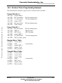
10.1 Protocol Timer Architecture . . . . . . . . . . . . . . . . . . . . . . . . . . . . . . . . . . . . . . . 10-1
10.1.1
Timing Signals and Components . . . . . . . . . . . . . . . . . . . . . . . . . . . . . . . . . 10-3
10.1.2
Event Table . . . . . . . . . . . . . . . . . . . . . . . . . . . . . . . . . . . . . . . . . . . . . . . . . 10-4
10.1.3
Event Generation . . . . . . . . . . . . . . . . . . . . . . . . . . . . . . . . . . . . . . . . . . . . . 10-4
10.2 PT Operation . . . . . . . . . . . . . . . . . . . . . . . . . . . . . . . . . . . . . . . . . . . . . . . . . . . 10-6
10.2.1
Frame Events . . . . . . . . . . . . . . . . . . . . . . . . . . . . . . . . . . . . . . . . . . . . . . . . 10-6
10.2.2
Macro Tables . . . . . . . . . . . . . . . . . . . . . . . . . . . . . . . . . . . . . . . . . . . . . . . . 10-7
10.2.3
Operating Modes . . . . . . . . . . . . . . . . . . . . . . . . . . . . . . . . . . . . . . . . . . . . 10-10
10.2.4
Error Detection. . . . . . . . . . . . . . . . . . . . . . . . . . . . . . . . . . . . . . . . . . . . . . 10-11
10.2.5
Interrupts . . . . . . . . . . . . . . . . . . . . . . . . . . . . . . . . . . . . . . . . . . . . . . . . . . 10-11
10.2.6
General Purpose Input/Output (GPIO). . . . . . . . . . . . . . . . . . . . . . . . . . . . 10-12
10.3 PT Event Codes . . . . . . . . . . . . . . . . . . . . . . . . . . . . . . . . . . . . . . . . . . . . . . . . 10-13
10.4 PT Registers. . . . . . . . . . . . . . . . . . . . . . . . . . . . . . . . . . . . . . . . . . . . . . . . . . . 10-15
10.4.1
PT Control Registers . . . . . . . . . . . . . . . . . . . . . . . . . . . . . . . . . . . . . . . . . 10-17
10.4.2
GPIO Registers. . . . . . . . . . . . . . . . . . . . . . . . . . . . . . . . . . . . . . . . . . . . . . 10-26
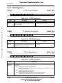
10.5 Protocol Timer Programming Example. . . . . . . . . . . . . . . . . . . . . . . . . . . . . . 10-27
Chapter 11
UART
11.1 UART Definitions . . . . . . . . . . . . . . . . . . . . . . . . . . . . . . . . . . . . . . . . . . . . . . .
11.2 UART Architecture . . . . . . . . . . . . . . . . . . . . . . . . . . . . . . . . . . . . . . . . . . . . . .
11.2.1
Transmitter . . . . . . . . . . . . . . . . . . . . . . . . . . . . . . . . . . . . . . . . . . . . . . . . . .
11.2.2
Receiver . . . . . . . . . . . . . . . . . . . . . . . . . . . . . . . . . . . . . . . . . . . . . . . . . . . .
11.2.3
Clock Generator . . . . . . . . . . . . . . . . . . . . . . . . . . . . . . . . . . . . . . . . . . . . . .
11.2.4
Infrared Interface . . . . . . . . . . . . . . . . . . . . . . . . . . . . . . . . . . . . . . . . . . . . .
11.2.5
UART Pins . . . . . . . . . . . . . . . . . . . . . . . . . . . . . . . . . . . . . . . . . . . . . . . . . .
11.2.6
Frame Configuration . . . . . . . . . . . . . . . . . . . . . . . . . . . . . . . . . . . . . . . . . .
11.3 UART Operation . . . . . . . . . . . . . . . . . . . . . . . . . . . . . . . . . . . . . . . . . . . . . . . .
11.3.1
Transmission . . . . . . . . . . . . . . . . . . . . . . . . . . . . . . . . . . . . . . . . . . . . . . . .
11.3.2
Reception . . . . . . . . . . . . . . . . . . . . . . . . . . . . . . . . . . . . . . . . . . . . . . . . . . .
11.3.3
UART Clocks. . . . . . . . . . . . . . . . . . . . . . . . . . . . . . . . . . . . . . . . . . . . . . . .
11.3.4
Baud Rate Detection (Autobaud) . . . . . . . . . . . . . . . . . . . . . . . . . . . . . . . . .
11.3.5
Low-Power Modes . . . . . . . . . . . . . . . . . . . . . . . . . . . . . . . . . . . . . . . . . . . .
Motorola
Table of Contents
For More Information On This Product,
Go to: www.freescale.com
11-1
11-2
11-3
11-3
11-4
11-4
11-4
11-4
11-5
11-5
11-5
11-6
11-6
11-7
vii
Freescale Semiconductor, Inc.
11.3.6
Debug Mode. . . . . . . . . . . . . . . . . . . . . . . . . . . . . . . . . . . . . . . . . . . . . . . . . 11-7
11.4 UART Registers. . . . . . . . . . . . . . . . . . . . . . . . . . . . . . . . . . . . . . . . . . . . . . . . . 11-8
11.4.1
UART Control Registers . . . . . . . . . . . . . . . . . . . . . . . . . . . . . . . . . . . . . . . 11-9
11.4.2
GPIO Registers. . . . . . . . . . . . . . . . . . . . . . . . . . . . . . . . . . . . . . . . . . . . . . 11-16
Freescale Semiconductor, Inc...
Chapter 12
Smart Card Port
12.1 SCP Architecture . . . . . . . . . . . . . . . . . . . . . . . . . . . . . . . . . . . . . . . . . . . . . . . . 12-1
12.1.1
SCP Pins. . . . . . . . . . . . . . . . . . . . . . . . . . . . . . . . . . . . . . . . . . . . . . . . . . . . 12-2
12.1.2
Data Communication . . . . . . . . . . . . . . . . . . . . . . . . . . . . . . . . . . . . . . . . . . 12-2
12.1.3
Power Up/Down. . . . . . . . . . . . . . . . . . . . . . . . . . . . . . . . . . . . . . . . . . . . . . 12-3
12.2 SCP Operation . . . . . . . . . . . . . . . . . . . . . . . . . . . . . . . . . . . . . . . . . . . . . . . . . . 12-3
12.2.1
Activation/Deactivation Control . . . . . . . . . . . . . . . . . . . . . . . . . . . . . . . . . 12-3
12.2.2
Clock Generation . . . . . . . . . . . . . . . . . . . . . . . . . . . . . . . . . . . . . . . . . . . . . 12-4
12.2.3
Data Transactions. . . . . . . . . . . . . . . . . . . . . . . . . . . . . . . . . . . . . . . . . . . . . 12-5
12.2.4
Low Power Modes . . . . . . . . . . . . . . . . . . . . . . . . . . . . . . . . . . . . . . . . . . . . 12-8
12.2.5
Interrupts . . . . . . . . . . . . . . . . . . . . . . . . . . . . . . . . . . . . . . . . . . . . . . . . . . . 12-9
12.3 SCP Registers . . . . . . . . . . . . . . . . . . . . . . . . . . . . . . . . . . . . . . . . . . . . . . . . . 12-10
12.3.1
SCP Control Registers . . . . . . . . . . . . . . . . . . . . . . . . . . . . . . . . . . . . . . . . 12-11
12.3.2
GPIO . . . . . . . . . . . . . . . . . . . . . . . . . . . . . . . . . . . . . . . . . . . . . . . . . . . . . 12-16
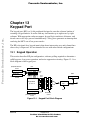
Chapter 13
Keypad Port
13.1 Keypad Operation . . . . . . . . . . . . . . . . . . . . . . . . . . . . . . . . . . . . . . . . . . . . . . .
13.1.1
Pin Configuration . . . . . . . . . . . . . . . . . . . . . . . . . . . . . . . . . . . . . . . . . . . . .
13.1.2
Keypad Matrix Polling . . . . . . . . . . . . . . . . . . . . . . . . . . . . . . . . . . . . . . . . .
13.1.3
Standby and Low Power Operation . . . . . . . . . . . . . . . . . . . . . . . . . . . . . . .
13.1.4
Noise Suppression on Keypad Inputs . . . . . . . . . . . . . . . . . . . . . . . . . . . . .
13.2 Keypad Port Registers . . . . . . . . . . . . . . . . . . . . . . . . . . . . . . . . . . . . . . . . . . . .
13-1
13-2
13-3
13-3
13-3
13-4
Chapter 14
Serial Audio and Baseband Ports
14.1 Data and Control Pins . . . . . . . . . . . . . . . . . . . . . . . . . . . . . . . . . . . . . . . . . . . .
14.2 Transmit and Receive Clocks . . . . . . . . . . . . . . . . . . . . . . . . . . . . . . . . . . . . . .
14.2.1
Clock Sources. . . . . . . . . . . . . . . . . . . . . . . . . . . . . . . . . . . . . . . . . . . . . . . .
14.2.2
Clock Frequency . . . . . . . . . . . . . . . . . . . . . . . . . . . . . . . . . . . . . . . . . . . . .
14.2.3
Clock Polarity. . . . . . . . . . . . . . . . . . . . . . . . . . . . . . . . . . . . . . . . . . . . . . . .
14.2.4
Bit Rate Multiplier (SAP Only) . . . . . . . . . . . . . . . . . . . . . . . . . . . . . . . . . .
14.3 TDM Options. . . . . . . . . . . . . . . . . . . . . . . . . . . . . . . . . . . . . . . . . . . . . . . . . . .
viii
DSP56652 UserÕs Manual
For More Information On This Product,
Go to: www.freescale.com
14-3
14-3
14-3
14-4
14-5
14-5
14-6
Motorola
Freescale Semiconductor, Inc...
Freescale Semiconductor, Inc.
14.3.1
Synchronous and Asynchronous Modes . . . . . . . . . . . . . . . . . . . . . . . . . . . 14-6
14.3.2
Frame Configuration . . . . . . . . . . . . . . . . . . . . . . . . . . . . . . . . . . . . . . . . . . 14-6
14.3.3
Frame Sync. . . . . . . . . . . . . . . . . . . . . . . . . . . . . . . . . . . . . . . . . . . . . . . . . . 14-7
14.3.4
Serial I/O Flags. . . . . . . . . . . . . . . . . . . . . . . . . . . . . . . . . . . . . . . . . . . . . . . 14-8
14.3.5
TDM Interrupts . . . . . . . . . . . . . . . . . . . . . . . . . . . . . . . . . . . . . . . . . . . . . . 14-8
14.4 Data Transmission and Reception . . . . . . . . . . . . . . . . . . . . . . . . . . . . . . . . . . . 14-9
14.4.1
Data Transmission . . . . . . . . . . . . . . . . . . . . . . . . . . . . . . . . . . . . . . . . . . . . 14-9
14.4.2
Data Reception . . . . . . . . . . . . . . . . . . . . . . . . . . . . . . . . . . . . . . . . . . . . . . 14-11
14.4.3
Data Formats . . . . . . . . . . . . . . . . . . . . . . . . . . . . . . . . . . . . . . . . . . . . . . . 14-12
14.5 Software Reset . . . . . . . . . . . . . . . . . . . . . . . . . . . . . . . . . . . . . . . . . . . . . . . . . 14-12
14.6 General-Purpose Timer (SAP Only) . . . . . . . . . . . . . . . . . . . . . . . . . . . . . . . . 14-13
14.7 Frame Counters (BBP Only) . . . . . . . . . . . . . . . . . . . . . . . . . . . . . . . . . . . . . . 14-13
14.8 Interrupts . . . . . . . . . . . . . . . . . . . . . . . . . . . . . . . . . . . . . . . . . . . . . . . . . . . . . 14-14
14.9 SAP and BBP Control Registers . . . . . . . . . . . . . . . . . . . . . . . . . . . . . . . . . . . 14-15
14.9.1
SAP and BBP Control Registers . . . . . . . . . . . . . . . . . . . . . . . . . . . . . . . . 14-17
14.9.2
GPIO Registers. . . . . . . . . . . . . . . . . . . . . . . . . . . . . . . . . . . . . . . . . . . . . . 14-24
Chapter 15
JTAG Port
15.1 DSP56600 Core JTAG Operation . . . . . . . . . . . . . . . . . . . . . . . . . . . . . . . . . . . 15-3
15.1.1
JTAG Pins . . . . . . . . . . . . . . . . . . . . . . . . . . . . . . . . . . . . . . . . . . . . . . . . . . 15-3
15.1.2
DSP TAP Controller. . . . . . . . . . . . . . . . . . . . . . . . . . . . . . . . . . . . . . . . . . . 15-4
15.1.3
Instruction Register . . . . . . . . . . . . . . . . . . . . . . . . . . . . . . . . . . . . . . . . . . . 15-5
15.2 Test Registers. . . . . . . . . . . . . . . . . . . . . . . . . . . . . . . . . . . . . . . . . . . . . . . . . . 15-10
15.2.1
Boundary Scan Register (BSR) . . . . . . . . . . . . . . . . . . . . . . . . . . . . . . . . . 15-10
15.2.2
Bypass Register . . . . . . . . . . . . . . . . . . . . . . . . . . . . . . . . . . . . . . . . . . . . . 15-10
15.2.3
Identification Register . . . . . . . . . . . . . . . . . . . . . . . . . . . . . . . . . . . . . . . . 15-10
15.3 DSP56652 JTAG Port Restrictions . . . . . . . . . . . . . . . . . . . . . . . . . . . . . . . . . 15-11
15.3.1
Normal Operation. . . . . . . . . . . . . . . . . . . . . . . . . . . . . . . . . . . . . . . . . . . . 15-11
15.3.2
Test Modes . . . . . . . . . . . . . . . . . . . . . . . . . . . . . . . . . . . . . . . . . . . . . . . . . 15-11
15.3.3
STOP Mode . . . . . . . . . . . . . . . . . . . . . . . . . . . . . . . . . . . . . . . . . . . . . . . . 15-11
15.4 MCU TAP Controller . . . . . . . . . . . . . . . . . . . . . . . . . . . . . . . . . . . . . . . . . . . 15-12
15.4.1
Entering MCU OnCE Mode via JTAG Control. . . . . . . . . . . . . . . . . . . . . 15-12
15.4.2
Release from Debug Mode for DSP and MCU . . . . . . . . . . . . . . . . . . . . . 15-13
Appendix A
DSP56652 DSP Bootloader
A.1 Boot Modes . . . . . . . . . . . . . . . . . . . . . . . . . . . . . . . . . . . . . . . . . . . . . . . . . . . . . A-1
A.2 Mode A: Normal MDI Boot . . . . . . . . . . . . . . . . . . . . . . . . . . . . . . . . . . . . . . . . A-2
A.2.1
Short and Long Messages . . . . . . . . . . . . . . . . . . . . . . . . . . . . . . . . . . . . . . . A-2
Motorola
Table of Contents
For More Information On This Product,
Go to: www.freescale.com
ix
Freescale Semiconductor, Inc.
A.2.2
Message Descriptions. . . . . . . . . . . . . . . . . . . . . . . . . . . . . . . . . . . . . . . . . . . A-4
A.2.3
Comments on Normal Boot Mode Usage . . . . . . . . . . . . . . . . . . . . . . . . . . A-13
A.2.4
Example of Program Download and Execution. . . . . . . . . . . . . . . . . . . . . . A-14
A.3 Mode B: Shared Memory Boot . . . . . . . . . . . . . . . . . . . . . . . . . . . . . . . . . . . . . A-15
A.4 Mode C: Messaging Unit Boot . . . . . . . . . . . . . . . . . . . . . . . . . . . . . . . . . . . . . A-16
A.5 Bootstrap Program . . . . . . . . . . . . . . . . . . . . . . . . . . . . . . . . . . . . . . . . . . . . . . . A-17
Freescale Semiconductor, Inc...
Appendix B
Equates and Header Files
B.1
B.2
B.3
MCU Equates. . . . . . . . . . . . . . . . . . . . . . . . . . . . . . . . . . . . . . . . . . . . . . . . . . . . B-1
MCU Include File . . . . . . . . . . . . . . . . . . . . . . . . . . . . . . . . . . . . . . . . . . . . . . . B-22
DSP Equates . . . . . . . . . . . . . . . . . . . . . . . . . . . . . . . . . . . . . . . . . . . . . . . . . . . B-32
Appendix C
Boundary Scan Register
C.1
C.2
BSR Bit Definitions. . . . . . . . . . . . . . . . . . . . . . . . . . . . . . . . . . . . . . . . . . . . . . . C-1
Boundary Scan Description Language . . . . . . . . . . . . . . . . . . . . . . . . . . . . . . . . C-4
Appendix D
ProgrammerÕs Reference
D.1
D.2
D.3
D.4
D.5
D.6
MCU Instruction Reference Tables . . . . . . . . . . . . . . . . . . . . . . . . . . . . . . . . . . . D-1
DSP Instruction Reference Tables. . . . . . . . . . . . . . . . . . . . . . . . . . . . . . . . . . . . D-7
MCU Internal I/O Memory Map . . . . . . . . . . . . . . . . . . . . . . . . . . . . . . . . . . . . D-14
DSP Internal I/O Memory Map . . . . . . . . . . . . . . . . . . . . . . . . . . . . . . . . . . . . . D-19
Register Index . . . . . . . . . . . . . . . . . . . . . . . . . . . . . . . . . . . . . . . . . . . . . . . . . . D-22
Acronym Changes . . . . . . . . . . . . . . . . . . . . . . . . . . . . . . . . . . . . . . . . . . . . . . . D-26
Appendix E
ProgrammerÕs Data Sheets
x
DSP56652 UserÕs Manual
For More Information On This Product,
Go to: www.freescale.com
Motorola
Freescale Semiconductor, Inc.
Freescale Semiconductor, Inc...
List of Figures
Figure 1-1.
DSP56652 Block Diagram . . . . . . . . . . . . . . . . . . . . . . . . . . . . . . . . . . . . 1-2
Figure 2-1.
Signal Group Organization . . . . . . . . . . . . . . . . . . . . . . . . . . . . . . . . . . . . 2-2
Figure 3-1.
MCU Memory Map . . . . . . . . . . . . . . . . . . . . . . . . . . . . . . . . . . . . . . . . . 3-2
Figure 3-2.
DSP Memory Map . . . . . . . . . . . . . . . . . . . . . . . . . . . . . . . . . . . . . . . . . . 3-5
Figure 4-1.
DSP56652 Clock Scheme . . . . . . . . . . . . . . . . . . . . . . . . . . . . . . . . . . . . . 4-2
Figure 4-2.
DSP PLL and Clock Generator. . . . . . . . . . . . . . . . . . . . . . . . . . . . . . . . . 4-3
Figure 4-3.
DSP56652 Reset Circuit . . . . . . . . . . . . . . . . . . . . . . . . . . . . . . . . . . . . . 4-10
Figure 4-4.
MUX Connectivity Scheme . . . . . . . . . . . . . . . . . . . . . . . . . . . . . . . . . . 4-17
Figure 5-1.
MDI Block Diagram . . . . . . . . . . . . . . . . . . . . . . . . . . . . . . . . . . . . . . . . . 5-1
Figure 5-2.
MDI: DSP-Side Memory Mapping. . . . . . . . . . . . . . . . . . . . . . . . . . . . . . 5-2
Figure 5-3.
MDI: MCU-Side Memory Mapping . . . . . . . . . . . . . . . . . . . . . . . . . . . . . 5-3
Figure 5-4.
MDI Register Symmetry. . . . . . . . . . . . . . . . . . . . . . . . . . . . . . . . . . . . . . 5-7
Figure 5-5.
MDI Message Exchange . . . . . . . . . . . . . . . . . . . . . . . . . . . . . . . . . . . . . . 5-8
Figure 5-6.
DSP-to-MCU General Purpose Interrupt . . . . . . . . . . . . . . . . . . . . . . . . . 5-9
Figure 6-1.
EIM Block Diagram . . . . . . . . . . . . . . . . . . . . . . . . . . . . . . . . . . . . . . . . . 6-1
Figure 6-2.
Example EIM Interface to Memory and Peripherals . . . . . . . . . . . . . . . . 6-2
Figure 7-1.
MCU Interrupt Controller . . . . . . . . . . . . . . . . . . . . . . . . . . . . . . . . . . . . . 7-2
Figure 7-2.
Hardware Priority Flowchart . . . . . . . . . . . . . . . . . . . . . . . . . . . . . . . . . . 7-3
Figure 7-3.
Internal IRQAÐD Connection . . . . . . . . . . . . . . . . . . . . . . . . . . . . . . . . . 7-11
Figure 7-4.
Edge I/O Pin . . . . . . . . . . . . . . . . . . . . . . . . . . . . . . . . . . . . . . . . . . . . . . 7-16
Figure 8-1.
QSPI Signal Flow . . . . . . . . . . . . . . . . . . . . . . . . . . . . . . . . . . . . . . . . . . . 8-5
Figure 8-2.
QSPI Serial Transfer Timing . . . . . . . . . . . . . . . . . . . . . . . . . . . . . . . . . 8-21
Figure 9-1.
PIT Block Diagram . . . . . . . . . . . . . . . . . . . . . . . . . . . . . . . . . . . . . . . . . . 9-2
Figure 9-2.
PIT Timing Using the PITMR . . . . . . . . . . . . . . . . . . . . . . . . . . . . . . . . . 9-2
Figure 9-3.
Watchdog Timer Block Diagram . . . . . . . . . . . . . . . . . . . . . . . . . . . . . . . 9-5
Figure 9-4.
GP Timer/PWM Clocks . . . . . . . . . . . . . . . . . . . . . . . . . . . . . . . . . . . . . . 9-7
Figure 9-5.
GP Timer Block Diagram . . . . . . . . . . . . . . . . . . . . . . . . . . . . . . . . . . . . . 9-9
Motorola
List of Figures
For More Information On This Product,
Go to: www.freescale.com
xi
Freescale Semiconductor, Inc.
Figure 9-6.
PWM Block Diagram . . . . . . . . . . . . . . . . . . . . . . . . . . . . . . . . . . . . . . . 9-12
Figure 10-1. Protocol Timer Block Diagram . . . . . . . . . . . . . . . . . . . . . . . . . . . . . . . 10-2
Figure 10-2. Event Table Structure . . . . . . . . . . . . . . . . . . . . . . . . . . . . . . . . . . . . . . . 10-5
Figure 10-3. Frame Table Entry . . . . . . . . . . . . . . . . . . . . . . . . . . . . . . . . . . . . . . . . . 10-7
Figure 10-4. Macro Table Entry . . . . . . . . . . . . . . . . . . . . . . . . . . . . . . . . . . . . . . . . . 10-8
Figure 10-5. Delay Table Entry. . . . . . . . . . . . . . . . . . . . . . . . . . . . . . . . . . . . . . . . . . 10-9
Figure 11-1. UART Block Diagram . . . . . . . . . . . . . . . . . . . . . . . . . . . . . . . . . . . . . . 11-3
Freescale Semiconductor, Inc...
Figure 12-1. Smart Card Port Interface . . . . . . . . . . . . . . . . . . . . . . . . . . . . . . . . . . . . 12-1
Figure 12-2. SCP: Port Interface and Auto Power Down Logic . . . . . . . . . . . . . . . . . 12-3
Figure 12-3. SCP: Clocks and Data. . . . . . . . . . . . . . . . . . . . . . . . . . . . . . . . . . . . . . . 12-5
Figure 12-4. SCP Data Formats . . . . . . . . . . . . . . . . . . . . . . . . . . . . . . . . . . . . . . . . . 12-8
Figure 12-5. SCP Interrupts. . . . . . . . . . . . . . . . . . . . . . . . . . . . . . . . . . . . . . . . . . . . . 12-9
Figure 13-1. Keypad Port Block Diagram. . . . . . . . . . . . . . . . . . . . . . . . . . . . . . . . . . 13-1
Figure 13-2. Glitch Suppressor Functional Diagram . . . . . . . . . . . . . . . . . . . . . . . . . 13-4
Figure 14-1. SAP Block Diagram . . . . . . . . . . . . . . . . . . . . . . . . . . . . . . . . . . . . . . . . 14-2
Figure 14-2. BBP Block Diagram . . . . . . . . . . . . . . . . . . . . . . . . . . . . . . . . . . . . . . . . 14-2
Figure 15-1. DSP56652 JTAG Block Diagram. . . . . . . . . . . . . . . . . . . . . . . . . . . . . . 15-2
Figure 15-2. DSP56600 Core JTAG Block Diagram . . . . . . . . . . . . . . . . . . . . . . . . . 15-3
Figure 15-3. TAP Controller State Machine . . . . . . . . . . . . . . . . . . . . . . . . . . . . . . . . 15-5
Figure 15-4. JTAG Instruction Register . . . . . . . . . . . . . . . . . . . . . . . . . . . . . . . . . . . 15-5
Figure 15-5. JTAG Bypass Register . . . . . . . . . . . . . . . . . . . . . . . . . . . . . . . . . . . . . 15-10
Figure 15-6. JTAG ID Register . . . . . . . . . . . . . . . . . . . . . . . . . . . . . . . . . . . . . . . . . 15-11
Figure A-1. Short Message Format . . . . . . . . . . . . . . . . . . . . . . . . . . . . . . . . . . . . . . . A-3
Figure A-2. Long Message Format . . . . . . . . . . . . . . . . . . . . . . . . . . . . . . . . . . . . . . . A-3
Figure A-3. Format of memory_write.request Message . . . . . . . . . . . . . . . . . . . . . . . A-5
Figure A-4.
Format of message_write.response Message. . . . . . . . . . . . . . . . . . . . . . A-6
Figure A-5.
Format of memory_read.request Message. . . . . . . . . . . . . . . . . . . . . . . . A-7
Figure A-6.
Format of memory_read.response Message . . . . . . . . . . . . . . . . . . . . . . A-8
Figure A-7.
Format of memory_check.request Message . . . . . . . . . . . . . . . . . . . . . . A-9
Figure A-8.
Format of memory_check.request Message . . . . . . . . . . . . . . . . . . . . . A-10
Figure A-9.
Format of start_application.request Message . . . . . . . . . . . . . . . . . . . . A-11
xii
DSP56652 UserÕs Manual
For More Information On This Product,
Go to: www.freescale.com
Motorola
Freescale Semiconductor, Inc.
Figure A-10. Format of invalid_opcode.response Message . . . . . . . . . . . . . . . . . . . . A-12
Freescale Semiconductor, Inc...
Figure A-11. Mapping of DSP Program Memory words to MDI message words. . . . A-13
Motorola
List of Figures
For More Information On This Product,
Go to: www.freescale.com
xiii
Freescale Semiconductor, Inc...
Freescale Semiconductor, Inc.
xiv
DSP56652 UserÕs Manual
For More Information On This Product,
Go to: www.freescale.com
Motorola
Freescale Semiconductor, Inc.
Freescale Semiconductor, Inc...
List of Tables
Table 2-1.
DSP56652 Signal Functional Group Allocations . . . . . . . . . . . . . . . . . . . 2-1
Table 2-2.
Power . . . . . . . . . . . . . . . . . . . . . . . . . . . . . . . . . . . . . . . . . . . . . . . . . . . . 2-3
Table 2-3.
Ground . . . . . . . . . . . . . . . . . . . . . . . . . . . . . . . . . . . . . . . . . . . . . . . . . . 2-4
Table 2-4.
PLL and Clock Signals . . . . . . . . . . . . . . . . . . . . . . . . . . . . . . . . . . . . . . 2-5
Table 2-5.
Address and Data Buses . . . . . . . . . . . . . . . . . . . . . . . . . . . . . . . . . . . . . . 2-6
Table 2-6.
Bus Control . . . . . . . . . . . . . . . . . . . . . . . . . . . . . . . . . . . . . . . . . . . . . . . . 2-6
Table 2-7.
Chip Select Signals . . . . . . . . . . . . . . . . . . . . . . . . . . . . . . . . . . . . . . . . . 2-6
Table 2-8.
Reset, Mode, and Multiplexer Control Signals . . . . . . . . . . . . . . . . . . . . 2-7
Table 2-9.
Interrupt Signals . . . . . . . . . . . . . . . . . . . . . . . . . . . . . . . . . . . . . . . . . . . 2-8
Table 2-10. Protocol Timer Output Signals . . . . . . . . . . . . . . . . . . . . . . . . . . . . . . . . . 2-9
Table 2-11. Keypad Port Signals . . . . . . . . . . . . . . . . . . . . . . . . . . . . . . . . . . . . . . . 2-10
Table 2-12. UART Signals . . . . . . . . . . . . . . . . . . . . . . . . . . . . . . . . . . . . . . . . . . . . 2-13
Table 2-13. QSPI Signals . . . . . . . . . . . . . . . . . . . . . . . . . . . . . . . . . . . . . . . . . . . . . 2-15
Table 2-14. SCP Signals . . . . . . . . . . . . . . . . . . . . . . . . . . . . . . . . . . . . . . . . . . . . . . 2-16
Table 2-15. SAP Signals . . . . . . . . . . . . . . . . . . . . . . . . . . . . . . . . . . . . . . . . . . . . . . 2-16
Table 2-16. BBP Signals . . . . . . . . . . . . . . . . . . . . . . . . . . . . . . . . . . . . . . . . . . . . . . 2-18
Table 2-17. Emulation Port Signals . . . . . . . . . . . . . . . . . . . . . . . . . . . . . . . . . . . . . 2-18
Table 2-18. Debug Control Signals . . . . . . . . . . . . . . . . . . . . . . . . . . . . . . . . . . . . . . 2-19
Table 2-19. JTAG Port Signals . . . . . . . . . . . . . . . . . . . . . . . . . . . . . . . . . . . . . . . . . 2-19
Table 4-1.
MCU and MCU Peripherals Clock Source . . . . . . . . . . . . . . . . . . . . . . . . 4-3
Table 4-2.
CKCTL Description . . . . . . . . . . . . . . . . . . . . . . . . . . . . . . . . . . . . . . . . . 4-5
Table 4-3.
PCTL0 Descriptions . . . . . . . . . . . . . . . . . . . . . . . . . . . . . . . . . . . . . . . . . 4-6
Table 4-4.
PCTL1 Description . . . . . . . . . . . . . . . . . . . . . . . . . . . . . . . . . . . . . . . . . . 4-7
Table 4-5.
MCU Peripherals in Low Power Mode. . . . . . . . . . . . . . . . . . . . . . . . . . . 4-8
Table 4-6.
DSP Peripherals in Low Power Modes. . . . . . . . . . . . . . . . . . . . . . . . . . . 4-8
Table 4-7.
Programmable Power-Saving Features. . . . . . . . . . . . . . . . . . . . . . . . . . . 4-9
Table 4-8.
RSR Description . . . . . . . . . . . . . . . . . . . . . . . . . . . . . . . . . . . . . . . . . . . 4-11
Motorola
List of Tables
For More Information On This Product,
Go to: www.freescale.com
xv
Freescale Semiconductor, Inc.
Table 4-9.
OMR Description . . . . . . . . . . . . . . . . . . . . . . . . . . . . . . . . . . . . . . . . . . 4-13
Table 4-10. Patch JUMP Targets . . . . . . . . . . . . . . . . . . . . . . . . . . . . . . . . . . . . . . . 4-14
Table 4-11. Debug Port Pin Multiplexing . . . . . . . . . . . . . . . . . . . . . . . . . . . . . . . . . 4-16
Table 4-12. Timer Pin Multiplexing . . . . . . . . . . . . . . . . . . . . . . . . . . . . . . . . . . . . . 4-16
Table 4-13. GPCR Description . . . . . . . . . . . . . . . . . . . . . . . . . . . . . . . . . . . . . . . . . 4-18
Freescale Semiconductor, Inc...
Table 4-14. Pin Function in DSP Address Visibility Mode. . . . . . . . . . . . . . . . . . . . 4-20
Table 5-1.
MCU MDI Access Timing . . . . . . . . . . . . . . . . . . . . . . . . . . . . . . . . . . . . 5-6
Table 5-2.
MDI Registers and Symmetry . . . . . . . . . . . . . . . . . . . . . . . . . . . . . . . . . 5-7
Table 5-3.
MCU Wake-up Events . . . . . . . . . . . . . . . . . . . . . . . . . . . . . . . . . . . . . . 5-12
Table 5-4.
MDI Reset Sources . . . . . . . . . . . . . . . . . . . . . . . . . . . . . . . . . . . . . . . . . 5-14
Table 5-5.
General Restrictions . . . . . . . . . . . . . . . . . . . . . . . . . . . . . . . . . . . . . . . . 5-15
Table 5-6.
DSP-Side Restrictions . . . . . . . . . . . . . . . . . . . . . . . . . . . . . . . . . . . . . . 5-15
Table 5-7.
MCU-Side Restrictions . . . . . . . . . . . . . . . . . . . . . . . . . . . . . . . . . . . . . 5-16
Table 5-8.
MDI Signalling and Control Registers . . . . . . . . . . . . . . . . . . . . . . . . . . 5-17
Table 5-9.
MCUÐDSP Register Correspondence . . . . . . . . . . . . . . . . . . . . . . . . . . 5-17
Table 5-10. MCVR Description. . . . . . . . . . . . . . . . . . . . . . . . . . . . . . . . . . . . . . . . . 5-18
Table 5-11. MCR Description . . . . . . . . . . . . . . . . . . . . . . . . . . . . . . . . . . . . . . . . . . 5-19
Table 5-12. MSR Description . . . . . . . . . . . . . . . . . . . . . . . . . . . . . . . . . . . . . . . . . . 5-21
Table 5-13. MTR1 Description . . . . . . . . . . . . . . . . . . . . . . . . . . . . . . . . . . . . . . . . . 5-24
Table 5-14. MTR0 Description . . . . . . . . . . . . . . . . . . . . . . . . . . . . . . . . . . . . . . . . . 5-24
Table 5-15. MRR1 Description . . . . . . . . . . . . . . . . . . . . . . . . . . . . . . . . . . . . . . . . . 5-24
Table 5-16. MRR0 Description . . . . . . . . . . . . . . . . . . . . . . . . . . . . . . . . . . . . . . . . . 5-24
Table 5-17. DCR Description . . . . . . . . . . . . . . . . . . . . . . . . . . . . . . . . . . . . . . . . . . 5-25
Table 5-18. DSR Description . . . . . . . . . . . . . . . . . . . . . . . . . . . . . . . . . . . . . . . . . . 5-26
Table 5-19. DTR1 Description. . . . . . . . . . . . . . . . . . . . . . . . . . . . . . . . . . . . . . . . . . 5-28
Table 5-20. DTR0 Description. . . . . . . . . . . . . . . . . . . . . . . . . . . . . . . . . . . . . . . . . . 5-28
Table 5-21. DRR1 Description . . . . . . . . . . . . . . . . . . . . . . . . . . . . . . . . . . . . . . . . . 5-28
Table 5-22. DRR0 Description . . . . . . . . . . . . . . . . . . . . . . . . . . . . . . . . . . . . . . . . . 5-28
Table 6-1.
EIM Signal Description . . . . . . . . . . . . . . . . . . . . . . . . . . . . . . . . . . . . . . 6-3
Table 6-2.
Chip Select Address Range . . . . . . . . . . . . . . . . . . . . . . . . . . . . . . . . . . 6-4
Table 6-3.
Interface Requirements for Read and Write Cycles . . . . . . . . . . . . . . . . . 6-6
xvi
DSP56652 UserÕs Manual
For More Information On This Product,
Go to: www.freescale.com
Motorola
Freescale Semiconductor, Inc...
Freescale Semiconductor, Inc.
Table 6-4.
SIZ[1:0] Encoding . . . . . . . . . . . . . . . . . . . . . . . . . . . . . . . . . . . . . . . . . . 6-8
Table 6-5.
PSTAT[3:0] Encoding . . . . . . . . . . . . . . . . . . . . . . . . . . . . . . . . . . . . . . . 6-8
Table 6-6.
CSCRn Description . . . . . . . . . . . . . . . . . . . . . . . . . . . . . . . . . . . . . . . . . 6-9
Table 6-7.
EIMCR Description . . . . . . . . . . . . . . . . . . . . . . . . . . . . . . . . . . . . . . . . 6-12
Table 6-8.
QDDR Description . . . . . . . . . . . . . . . . . . . . . . . . . . . . . . . . . . . . . . . . . 6-13
Table 6-9.
QPDR Description . . . . . . . . . . . . . . . . . . . . . . . . . . . . . . . . . . . . . . . . . 6-13
Table 7-1.
MCU Interrupt Sources . . . . . . . . . . . . . . . . . . . . . . . . . . . . . . . . . . . . . . 7-4
Table 7-2.
ISR Description . . . . . . . . . . . . . . . . . . . . . . . . . . . . . . . . . . . . . . . . . . . . 7-6
Table 7-3.
NIER/FIER Description . . . . . . . . . . . . . . . . . . . . . . . . . . . . . . . . . . . . . . 7-8
Table 7-4.
NIPR and FIPR Description . . . . . . . . . . . . . . . . . . . . . . . . . . . . . . . . . . 7-9
Table 7-5.
ICR Description . . . . . . . . . . . . . . . . . . . . . . . . . . . . . . . . . . . . . . . . . . . 7-10
Table 7-6.
DSP Interrupt Sources . . . . . . . . . . . . . . . . . . . . . . . . . . . . . . . . . . . . . . 7-11
Table 7-7.
Interrupt Source Priorities within an IPL . . . . . . . . . . . . . . . . . . . . . . . . 7-13
Table 7-8.
IPRP Description . . . . . . . . . . . . . . . . . . . . . . . . . . . . . . . . . . . . . . . . . . 7-14
Table 7-9.
IPRC Description . . . . . . . . . . . . . . . . . . . . . . . . . . . . . . . . . . . . . . . . . . 7-15
Table 7-10. EPPAR Description . . . . . . . . . . . . . . . . . . . . . . . . . . . . . . . . . . . . . . . . 7-17
Table 7-11. EPDDR Description . . . . . . . . . . . . . . . . . . . . . . . . . . . . . . . . . . . . . . . . 7-17
Table 7-12. EPDR Description . . . . . . . . . . . . . . . . . . . . . . . . . . . . . . . . . . . . . . . . . 7-18
Table 7-13. EPFR Description . . . . . . . . . . . . . . . . . . . . . . . . . . . . . . . . . . . . . . . . . . 7-18
Table 8-1.
Serial Control Port Signals . . . . . . . . . . . . . . . . . . . . . . . . . . . . . . . . . . . 8-4
Table 8-2.
QSPI Register/Memory Summary . . . . . . . . . . . . . . . . . . . . . . . . . . . . . 8-12
Table 8-3.
SPCR Description . . . . . . . . . . . . . . . . . . . . . . . . . . . . . . . . . . . . . . . . . 8-13
Table 8-4.
QCR Description . . . . . . . . . . . . . . . . . . . . . . . . . . . . . . . . . . . . . . . . . . 8-15
Table 8-5.
SPSR Description . . . . . . . . . . . . . . . . . . . . . . . . . . . . . . . . . . . . . . . . . 8-17
Table 8-6.
SCCR Description . . . . . . . . . . . . . . . . . . . . . . . . . . . . . . . . . . . . . . . . . 8-19
Table 8-7.
QSPI Control RAM Description . . . . . . . . . . . . . . . . . . . . . . . . . . . . . . 8-22
Table 8-8.
QPCR Description . . . . . . . . . . . . . . . . . . . . . . . . . . . . . . . . . . . . . . . . . 8-24
Table 8-9.
QDDR Description . . . . . . . . . . . . . . . . . . . . . . . . . . . . . . . . . . . . . . . . . 8-25
Table 8-10. QPDR Description . . . . . . . . . . . . . . . . . . . . . . . . . . . . . . . . . . . . . . . . . 8-25
Table 9-1.
ITCSR Description . . . . . . . . . . . . . . . . . . . . . . . . . . . . . . . . . . . . . . . . . . 9-3
Table 9-2.
WCR Description . . . . . . . . . . . . . . . . . . . . . . . . . . . . . . . . . . . . . . . . . . . 9-6
Motorola
List of Tables
For More Information On This Product,
Go to: www.freescale.com
xvii
Freescale Semiconductor, Inc.
Table 9-3.
TPWCR Description. . . . . . . . . . . . . . . . . . . . . . . . . . . . . . . . . . . . . . . . 9-13
Table 9-4.
TPWMR Description . . . . . . . . . . . . . . . . . . . . . . . . . . . . . . . . . . . . . . . 9-14
Table 9-5.
TPWSR Description . . . . . . . . . . . . . . . . . . . . . . . . . . . . . . . . . . . . . . . . 9-15
Table 9-6.
GNRC Description . . . . . . . . . . . . . . . . . . . . . . . . . . . . . . . . . . . . . . . . . 9-16
Table 10-1. Protocol Timer Operation Mode Summary . . . . . . . . . . . . . . . . . . . . . 10-10
Table 10-2. Protocol Timer Interrupt Sources . . . . . . . . . . . . . . . . . . . . . . . . . . . . . 10-12
Table 10-3. PT Port Pin Assignment . . . . . . . . . . . . . . . . . . . . . . . . . . . . . . . . . . . . 10-13
Freescale Semiconductor, Inc...
Table 10-4. Protocol Timer Event List . . . . . . . . . . . . . . . . . . . . . . . . . . . . . . . . . . 10-13
Table 10-5. Protocol Timer Register Summary . . . . . . . . . . . . . . . . . . . . . . . . . . . . 10-15
Table 10-6. PTCR Description. . . . . . . . . . . . . . . . . . . . . . . . . . . . . . . . . . . . . . . . . 10-17
Table 10-7. Additional Conditions for Generating PT Interrupts . . . . . . . . . . . . . . 10-18
Table 10-8. PTIER Description . . . . . . . . . . . . . . . . . . . . . . . . . . . . . . . . . . . . . . . . 10-19
Table 10-9. PTSR Description . . . . . . . . . . . . . . . . . . . . . . . . . . . . . . . . . . . . . . . . . 10-20
Table 10-10. PTEVR Description . . . . . . . . . . . . . . . . . . . . . . . . . . . . . . . . . . . . . . . 10-21
Table 10-11. TIMR Description. . . . . . . . . . . . . . . . . . . . . . . . . . . . . . . . . . . . . . . . . 10-21
Table 10-12. CTIC Description . . . . . . . . . . . . . . . . . . . . . . . . . . . . . . . . . . . . . . . . . 10-22
Table 10-13. CTIMR Description . . . . . . . . . . . . . . . . . . . . . . . . . . . . . . . . . . . . . . . 10-22
Table 10-14. CFC Description . . . . . . . . . . . . . . . . . . . . . . . . . . . . . . . . . . . . . . . . . . 10-22
Table 10-15. CFMR Description . . . . . . . . . . . . . . . . . . . . . . . . . . . . . . . . . . . . . . . . 10-23
Table 10-16. RSC Description . . . . . . . . . . . . . . . . . . . . . . . . . . . . . . . . . . . . . . . . . . 10-23
Table 10-17. RSMR Description . . . . . . . . . . . . . . . . . . . . . . . . . . . . . . . . . . . . . . . . 10-23
Table 10-18. FTPTR Description. . . . . . . . . . . . . . . . . . . . . . . . . . . . . . . . . . . . . . . . 10-24
Table 10-19. MTPTR Description . . . . . . . . . . . . . . . . . . . . . . . . . . . . . . . . . . . . . . . 10-24
Table 10-20. FTBAR Description . . . . . . . . . . . . . . . . . . . . . . . . . . . . . . . . . . . . . . . 10-24
Table 10-21. MTBAR Description . . . . . . . . . . . . . . . . . . . . . . . . . . . . . . . . . . . . . . 10-25
Table 10-22. DTPTR Description . . . . . . . . . . . . . . . . . . . . . . . . . . . . . . . . . . . . . . . 10-25
Table 10-23. PTPCR Description . . . . . . . . . . . . . . . . . . . . . . . . . . . . . . . . . . . . . . . 10-26
Table 10-24. PTDDR Description . . . . . . . . . . . . . . . . . . . . . . . . . . . . . . . . . . . . . . . 10-26
Table 10-25. PTPDR Description . . . . . . . . . . . . . . . . . . . . . . . . . . . . . . . . . . . . . . . 10-26
Table 11-1. Suggested GPIO Pins for UART Signals . . . . . . . . . . . . . . . . . . . . . . . . 11-4
Table 11-2. UART Low Power Mode Operation . . . . . . . . . . . . . . . . . . . . . . . . . . . 11-7
xviii
DSP56652 UserÕs Manual
For More Information On This Product,
Go to: www.freescale.com
Motorola
Freescale Semiconductor, Inc.
Table 11-3. UART Register Summary. . . . . . . . . . . . . . . . . . . . . . . . . . . . . . . . . . . . 11-8
Table 11-4. URX Description . . . . . . . . . . . . . . . . . . . . . . . . . . . . . . . . . . . . . . . . . . 11-9
Table 11-5. UTX Description . . . . . . . . . . . . . . . . . . . . . . . . . . . . . . . . . . . . . . . . . 11-10
Table 11-6. UCR1 Description . . . . . . . . . . . . . . . . . . . . . . . . . . . . . . . . . . . . . . . . 11-11
Table 11-7. UCR2 Description . . . . . . . . . . . . . . . . . . . . . . . . . . . . . . . . . . . . . . . . 11-13
Table 11-8. UBRGR Description. . . . . . . . . . . . . . . . . . . . . . . . . . . . . . . . . . . . . . . 11-14
Table 11-9. USR Description. . . . . . . . . . . . . . . . . . . . . . . . . . . . . . . . . . . . . . . . . . 11-14
Freescale Semiconductor, Inc...
Table 11-10. UTS Description . . . . . . . . . . . . . . . . . . . . . . . . . . . . . . . . . . . . . . . . . . 11-15
Table 11-11. UPCR Description . . . . . . . . . . . . . . . . . . . . . . . . . . . . . . . . . . . . . . . . 11-16
Table 11-12. UDDR Description . . . . . . . . . . . . . . . . . . . . . . . . . . . . . . . . . . . . . . . . 11-16
Table 11-13. UPDR Description . . . . . . . . . . . . . . . . . . . . . . . . . . . . . . . . . . . . . . . . 11-16
Table 12-1. SCP Register Summary . . . . . . . . . . . . . . . . . . . . . . . . . . . . . . . . . . . . 12-10
Table 12-2. SCPCR Description . . . . . . . . . . . . . . . . . . . . . . . . . . . . . . . . . . . . . . . 12-11
Table 12-3. SCACR Description . . . . . . . . . . . . . . . . . . . . . . . . . . . . . . . . . . . . . . . 12-12
Table 12-4. SCPIER Description . . . . . . . . . . . . . . . . . . . . . . . . . . . . . . . . . . . . . . . 12-13
Table 12-5. SCPSR Description . . . . . . . . . . . . . . . . . . . . . . . . . . . . . . . . . . . . . . . 12-14
Table 12-6. SCPDR Description . . . . . . . . . . . . . . . . . . . . . . . . . . . . . . . . . . . . . . . 12-15
Table 12-7. SCP Pin GPIO Bit Assignments . . . . . . . . . . . . . . . . . . . . . . . . . . . . . . 12-16
Table 12-8. SCPPCR Description . . . . . . . . . . . . . . . . . . . . . . . . . . . . . . . . . . . . . . 12-16
Table 13-1. Keypad Port pull-up Resistor Control . . . . . . . . . . . . . . . . . . . . . . . . . . 13-2
Table 13-2. Keypad Port Register Summary . . . . . . . . . . . . . . . . . . . . . . . . . . . . . . . 13-4
Table 13-3. KPCR Description . . . . . . . . . . . . . . . . . . . . . . . . . . . . . . . . . . . . . . . . . 13-5
Table 13-4. Generic Description . . . . . . . . . . . . . . . . . . . . . . . . . . . . . . . . . . . . . . . . 13-5
Table 13-5. KDDR Description . . . . . . . . . . . . . . . . . . . . . . . . . . . . . . . . . . . . . . . . . 13-6
Table 13-6. KPDR Description . . . . . . . . . . . . . . . . . . . . . . . . . . . . . . . . . . . . . . . . . 13-6
Table 14-1. SAP and BBP Pins . . . . . . . . . . . . . . . . . . . . . . . . . . . . . . . . . . . . . . . . . 14-3
Table 14-2. SAP/BBP Clock Sources . . . . . . . . . . . . . . . . . . . . . . . . . . . . . . . . . . . . 14-4
Table 14-3. Frame Configuration. . . . . . . . . . . . . . . . . . . . . . . . . . . . . . . . . . . . . . . . 14-6
Table 14-4. SAP and BBP Interrupts . . . . . . . . . . . . . . . . . . . . . . . . . . . . . . . . . . . . 14-14
Table 14-5. Serial Audio Port Register Summary . . . . . . . . . . . . . . . . . . . . . . . . . . 14-15
Table 14-6. Baseband Port Register Summary . . . . . . . . . . . . . . . . . . . . . . . . . . . . 14-16
Motorola
List of Tables
For More Information On This Product,
Go to: www.freescale.com
xix
Freescale Semiconductor, Inc.
Table 14-7. SAP/BBP CRA Description . . . . . . . . . . . . . . . . . . . . . . . . . . . . . . . . . 14-18
Table 14-8. SAP/BBP CRB Description . . . . . . . . . . . . . . . . . . . . . . . . . . . . . . . . . 14-19
Table 14-9. SAP/BBP CRC Description . . . . . . . . . . . . . . . . . . . . . . . . . . . . . . . . . 14-21
Table 14-10. SAP/BBP Status Register Description . . . . . . . . . . . . . . . . . . . . . . . . . 14-22
Table 14-11. SAP/BBP PDR Description . . . . . . . . . . . . . . . . . . . . . . . . . . . . . . . . . 14-24
Table 14-12. SAP/BBP DDR Description . . . . . . . . . . . . . . . . . . . . . . . . . . . . . . . . . 14-24
Table 14-13. SAP/BBP PCR Description . . . . . . . . . . . . . . . . . . . . . . . . . . . . . . . . . 14-25
Freescale Semiconductor, Inc...
Table 15-1. DSP JTAG Pins . . . . . . . . . . . . . . . . . . . . . . . . . . . . . . . . . . . . . . . . . . . 15-4
Table 15-2. JTAG Instructions . . . . . . . . . . . . . . . . . . . . . . . . . . . . . . . . . . . . . . . . . 15-6
Table 15-3. Entering MCU OnCE Mode . . . . . . . . . . . . . . . . . . . . . . . . . . . . . . . . 15-13
Table 15-4. Releasing the MCU and DSP from Debug Modes . . . . . . . . . . . . . . . 15-14
Table A-1.
DSP56652 Boot Modes . . . . . . . . . . . . . . . . . . . . . . . . . . . . . . . . . . . . . . A-2
Table A-2.
Message Summary . . . . . . . . . . . . . . . . . . . . . . . . . . . . . . . . . . . . . . . . . . A-4
Table A-3.
XYP Field . . . . . . . . . . . . . . . . . . . . . . . . . . . . . . . . . . . . . . . . . . . . . . . . . A-5
Table C-1.
BSR Bit Definitions . . . . . . . . . . . . . . . . . . . . . . . . . . . . . . . . . . . . . . . . . C-2
Table D-1.
MCU Instruction Set Summary . . . . . . . . . . . . . . . . . . . . . . . . . . . . . . . D-1
Table D-2.
MCU Instruction Syntax Notation . . . . . . . . . . . . . . . . . . . . . . . . . . . . . . D-6
Table D-3.
MCU Instruction Opcode Notation . . . . . . . . . . . . . . . . . . . . . . . . . . . . . D-6
Table D-4.
DSP Instruction Set Summary . . . . . . . . . . . . . . . . . . . . . . . . . . . . . . . . D-7
Table D-5.
Program Word and Timing Symbols . . . . . . . . . . . . . . . . . . . . . . . . . . . D-13
Table D-6.
Condition Code Register (CCR) Symbols . . . . . . . . . . . . . . . . . . . . . . . D-13
Table D-7.
Condition Code Register Notation . . . . . . . . . . . . . . . . . . . . . . . . . . . . D-13
Table D-8.
MCU Internal I/O Memory Map . . . . . . . . . . . . . . . . . . . . . . . . . . . . . D-14
Table D-9.
DSP Internal I/O Memory Map . . . . . . . . . . . . . . . . . . . . . . . . . . . . . . . D-19
Table D-10. Register Index . . . . . . . . . . . . . . . . . . . . . . . . . . . . . . . . . . . . . . . . . . . . D-22
Table D-11. DSP56652 Acronym Changes . . . . . . . . . . . . . . . . . . . . . . . . . . . . . . . . D-26
Table E-1.
xx
List of ProgrammerÕs Sheets . . . . . . . . . . . . . . . . . . . . . . . . . . . . . . . . . E-1
DSP56652 UserÕs Manual
For More Information On This Product,
Go to: www.freescale.com
Motorola
Freescale Semiconductor, Inc.
List of Examples
Example 5-1. Program Loop That Stalls MCU Access to Shared Memory . . . . . . . . . . 5-4
Example 5-2. Program Loop With No Stall . . . . . . . . . . . . . . . . . . . . . . . . . . . . . . . . . . 5-4
Example 5-3. Dummy Event to Allow MCU to Track DSP Power Mode Change . . . 5-13
Example 11-1.UART Baud Error Calculation . . . . . . . . . . . . . . . . . . . . . . . . . . . . . . . 11-6
Freescale Semiconductor, Inc...
Example A-1.Normal Boot . . . . . . . . . . . . . . . . . . . . . . . . . . . . . . . . . . . . . . . . . . . . . . A-14
Example A-2.Shared Memory Boot . . . . . . . . . . . . . . . . . . . . . . . . . . . . . . . . . . . . . . . A-15
Example A-3.Messaging Unit Boot . . . . . . . . . . . . . . . . . . . . . . . . . . . . . . . . . . . . . . . A-16
Motorola
List of Examples
For More Information On This Product,
Go to: www.freescale.com
xxi
Freescale Semiconductor, Inc...
Freescale Semiconductor, Inc.
xxii
DSP56652 UserÕs Manual
For More Information On This Product,
Go to: www.freescale.com
Motorola
Freescale Semiconductor, Inc.
Preface
Freescale Semiconductor, Inc...
This section provides information on the data conventions used in this manual, as well as a
list of complete product documentation.
Conventions
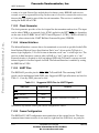
The following conventions are used in this manual:
¥
Bits within registers are always listed from most significant bit (MSB) to least
significant bit (LSB).
¥
1 byte = 8 bits
1 halfword = 16 bits = 2 bytes
1 word = 32 bits = 4 bytes
¥
Bits within a register are indicated AA[n:0] when more than one bit is involved in a
description. For purposes of description, the bits are presented as if they were
contiguous within a register, regardless of their actual physical locations in a
register.
¥
All bits in a register are read/write unless otherwise noted.
¥
When a bit is described as Òset,Ó its value is 1. When a bit is described as Òcleared,Ó
its value is 0.
¥
Register bits that are unused or reserved for future use are read as 0 and should be
written with 0 to ensure future compatibility. In the register descriptions, each of
these bits is indicated with a shaded box (
).
¥
The word ÒresetÓ is used in three different contexts in this manual:
Ñ There is a reset instruction that is always written as ÒRESETÓ.
Ñ In lower case, ÒresetÓ refers to the reset function. A leading capital letter is used
as grammar dictates.
Ñ ÒResetÓ refers to the Reset state.
¥
The word ÒpinÓ is a generic term for any pin on the chip. Because of on-chip pin
multiplexing, more than one signal may be present on any given pin.
¥
Pins or signals that are asserted low (made active when pulled to ground) have an
overbar over their name; for example, the SS0 pin is asserted low.
Motorola
xxiii
For More Information On This Product,
Go to: www.freescale.com
Freescale Semiconductor, Inc.
¥
Hex values are indicated with a dollar sign ($) preceding the hex value as follows:
X:$FFFF is the X memory address for the Interrupt Priority RegisterÑCore
(IPR-C).
Code examples are displayed in a monospaced font, as shown in Example 1.
Example 1.
Freescale Semiconductor, Inc...
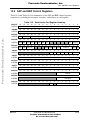
BFSET #$0007,X:PCC
Code Example
; Configure:
line 1
; MISO0, MOSI0, SCK0 for SPI masterline 2
; ~SS0 as PC3 for GPIO line 3
¥
In code examples, the names of pins or signals that are asserted low are preceded
by a tilde. In the previous example, line 3 refers to the SS0 pin (shown as ~SS0).
¥
The word ÒassertÓ means that a high true (active high) signal is pulled high to VCC
or that a low true (active low) signal is pulled low to ground. The word ÒdeassertÓ
means that a high true signal is pulled low to ground or that a low true signal is
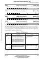
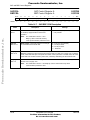
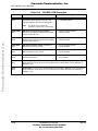
pulled high to VCC. These conventions are summarized in Table 1.
Table 1.
1.
2.
Signal States
Signal/Symbol
Logic State
Signal State
Voltage
PIN
True
Asserted
Ground1
PIN
False
Deasserted
VCC2
PIN
True
Asserted
VCC
PIN
False
Deasserted
Ground
Ground is an acceptable low-voltage level. See the appropriate data sheet
for the range of acceptable low-voltage levels (typically a TTL logic low).
VCC is an acceptable high-voltage level. See the appropriate data sheet for
the range of acceptable high-voltage levels (typically a TTL logic high).
Documentation
This manual (DSP56652UM/D) is one of a set of five documents that provides complete
product information for the DSP56652. The other four documents include the following:
xxiv
¥
M¥CORE Reference Manual (MCORERM/AD)
¥
MMC2001 Reference Manual (MMC2001M/AD
¥
DSP56600 Family Manual (DSP56600FM/AD)
¥
DSP56652 Technical Data Sheet (DSP56652/D)
DSP56652 UserÕs Manual
For More Information On This Product,
Go to: www.freescale.com
Motorola
Freescale Semiconductor, Inc.
Freescale Semiconductor, Inc...
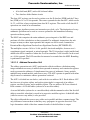
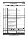
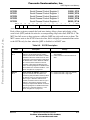
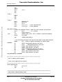
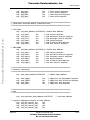
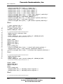
Chapter 1
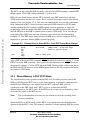
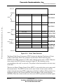
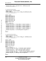
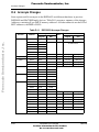
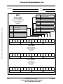
Introduction
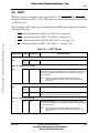
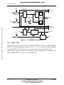
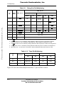
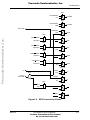
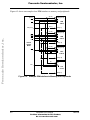
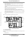
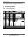
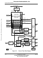
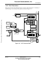
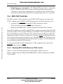
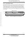
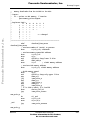
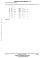
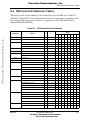
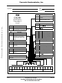
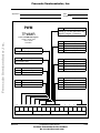
Motorola designed the ROM-based DSP56652 to support the rigorous demands of the
cellular subscriber market. The high level of on-chip integration in the DSP56652
minimizes application system design complexity and component count, resulting in very
compact implementations. This integration also yields very low power consumption and
cost-effective system performance. The DSP56652 chip combines MotorolaÕs 32-bit
M¥COREª MicroRISC Engine and the DSP56600 Digital Signal Processor (DSP) core
with on-chip memory, a protocol timer, and custom peripherals to provide a single-chip
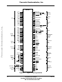
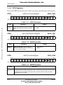
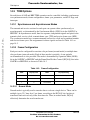
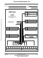
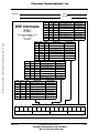
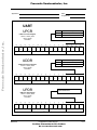
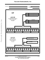
cellular base-band processor. A block diagram of the 56652 is shown in Figure 1-1.
1.1 DSP56652 Key Features
The following list summarizes the key features of the DSP56652.
¥
M¥CORE (MCU) core
Ñ 32-bit load/store M¥CORE RISC architecture
Ñ Fixed 16-bit instruction length
Ñ 16-entry 32-bit general-purpose register file
Ñ 32-bit internal address and data buses
Ñ Efficient four-stage, fully interlocked execution pipeline
Ñ Single-cycle execution for most instructions, two cycles for branches and
memory accesses
Ñ Special branch, byte, and bit manipulation instructions
Ñ Support for byte, halfword, and word memory accesses
Ñ Fast interrupt support via vectoring/auto-vectoring and a 16-entry dedicated
alternate register file
Motorola
Introduction
For More Information On This Product,
Go to: www.freescale.com
1-1
Freescale Semiconductor, Inc.
DSP56652 Key Features
Watchdog
Timer
Timer/PWM
Programmable
Interrupt Timer
Edge I/O
Smart Card
I/F
External
Memory
Keypad
I/F
M¥Core
MicroRISC
Core
RAM
512 x 32
Queued
SPI
Freescale Semiconductor, Inc...
ROM
4K x 32
UART
Clocks
DSP PLL
MUX
MCU Ð DSP
Interface
MCU
OnCE
JTAG
1K x 16 Dual-Port
X Data RAM
Messaging
Unit
MCU
OnCE
JTAG
X Data
RAM
(7+1)K x 16
X Data
ROM
10K x 16
Y Data
RAM
6K x 16
Y Data
ROM
10K x 16
Program
RAM
512 x 24
X Data
RAM
48K x 24
56600
DSP
Core
Serial
Audio
CODEC I/F
Protocol
Timer
Serial Audio
Codec I/F
DSP56652
Baseband
Codec I/F
Figure 1-1. DSP56652 Block Diagram
¥
DSP core
Ñ DSP56600 architecture
Ñ Single-cycle arithmetic instructions
Ñ Fully pipelined 16 ´ 16-bit parallel multiply accumulator (MAC)
Ñ Two 40-bit accumulators including extension bits
Ñ 40-bit parallel barrel shifter
Ñ Highly parallel instruction set with unique DSP addressing modes
Ñ Position-independent code support
Ñ Nested hardware DO loops
1-2
DSP56652 UserÕs Manual
For More Information On This Product,
Go to: www.freescale.com
Motorola
Freescale Semiconductor, Inc.
DSP56652 Key Features
Ñ Fast auto-return interrupts
Ñ On-chip support for software patching and enhancements
Ñ Real-time trace capability via external address bus
¥
On-chip memory
Ñ 4K ´ 32-bit MCU ROM
Ñ 512 ´ 32-bit MCU RAM
Ñ 48K ´ 24-bit DSP program ROM
Freescale Semiconductor, Inc...
Ñ 512 ´ 24-bit DSP program RAM
Ñ 10K ´ 16-bit DSP X data ROM
Ñ 10K ´ 16-bit DSP Y data ROM
Ñ (7+1)K ´ 16-bit X data RAM
Ñ 6K ´ 16-bit Y data RAM
¥
On-chip peripherals
Ñ Fully programmable phase-locked loop (PLL) for DSP clock generation
Ñ External interface module (EIM) for glueless system integration
Ñ External 22-bit address and 16-bit data MCU buses
Ñ 32-source MCU interrupt controller
Ñ Intelligent MCU/DSP interface (MDI) with 1K ´ 16-bit dual-port RAM as well
as messaging status and control unit
Ñ Serial audio codec port (SAP)
Ñ Serial baseband codec port (BBP)
Ñ Protocol timer frees the MCU from radio channel timing events
Ñ Queued serial peripheral interface (QSPI)
Ñ Keypad port capable of scanning up to an 8 ´ 8 matrix keypad
Ñ General-purpose MCU and DSP timers
Ñ Pulse width modulation (PWM) output
Ñ Universal asynchronous receiver/transmitter (UART) with FIFO
Ñ IEEE 1149.1-compliant boundary scan JTAG test access port (TAP)
Ñ Integrated DSP/MCU On-Chip Emulation (OnCEª) module
Ñ DSP program address bus visibility mode for system development
Ñ ISO 7816-compatible smart card port
Motorola
Introduction
For More Information On This Product,
Go to: www.freescale.com
1-3
Freescale Semiconductor, Inc.
Architecture Overview
¥
Operating features
Ñ Comprehensive static and dynamic power management
Ñ MCU operating frequency: DC to 16.8 MHz at 1.8 V
Ñ DSP operating frequency: DC to 58.8 MHz at 1.8 V
Ñ Internal operating voltage range: 1.8Ð2.5 V with 3.1 V-tolerant I/O
Ñ Operating temperature: Ð40û to 85ûC ambient
Freescale Semiconductor, Inc...
Ñ Package option: 15 ´ 15 mm, 196-lead PBGA
1.2 Architecture Overview
The DSP56652 combines the control and I/O capability of the M¥CORE MCU with the
data processing power of the DSP56600 core to provide a complete system solution for a
cellular baseband system. The DSP subsystem has a closed architecture, meaning that all
DSP memory is contained on the device and the DSP address and data buses do not appear
external to the device. The MCU subsystem provides both on-chip memory and an
external bus interface. Both processors provide external interrupt pins.
The two cores communicate through the MDI, which includes a block of dual-access
RAM.
Each core generates its own independent clock, and the DSP core contains a PLL as part
of its clock generation subsystem. Each processor and its associated peripherals have
several low-power standby modes.
A single JTAG port is shared by the two cores for debug and test purposes. The JTAG port
is integrated with on-chip emulation modules for both the MCU and the DSP, providing a
non-intrusive way to interact with the processors and their peripherals and memory. The
MCU has additional external debug pins for in-circuit emulation. The DSP program
address bus is multiplexed on other DSP56652 pins.
The pins associated with most peripherals can be programmed individually to function as
general-purpose input/output signals (GPIO) if their primary functions are not required.
(The exceptions are the MCU pulse width modulator and general-purpose timer, which
have no GPIO capability, and the SmartCard Port (SCP), whose five pins must all function
either as SCP pins or GPIO (i.e., cannot be individually programmed).
1.2.1 MCU
This section describes the MCU core, peripherals, and memory.
1-4
DSP56652 UserÕs Manual
For More Information On This Product,
Go to: www.freescale.com
Motorola
Freescale Semiconductor, Inc.
Architecture Overview
1.2.1.1 Core Description
Freescale Semiconductor, Inc...
The M¥CORE MCU utilizes a four-stage pipeline for instruction execution. The
instruction fetch, instruction decode/register file read, execute, and register write-back
stages operate in an overlapped fashion, allowing most instructions to execute in a single
clock cycle. Sixteen general-purpose registers are provided for source operands and
instruction results.
The execution unit consists of a 32-bit arithmetic/logic unit (ALU), a 32-bit barrel shifter,
a find-first-one unit (FFO), result feed-forward hardware, and miscellaneous support
hardware for multiplication and multiple register loads and stores. Arithmetic and logical
operations are executed in a single cycle with the exception of the multiply and divide
instructions. The FFO unit operates in a single clock cycle.
The program counter unit contains a PC incrementer and a dedicated branch address adder
to minimize delays during change-of-flow operations. Memory load and store operations
are provided for byte, halfword, and word (32-bit) data with automatic zero extension of
byte and halfword load data. These instructions can execute in two clock cycles. Load and
store multiple register instructions allow low overhead context save and restore
operations.
A single condition code/carry (C) bit is provided for condition testing and to implement
arithmetic and logical operations greater than 32 bits. A 16-entry alternate register file is
provided to minimize exception processing overhead, and the CPU supports both vectored
and auto-vectored interrupts.
The user programming model contains the program counter, sixteen 32-bit generalpurpose registers, and the carry bit. A separate supervisor mode is provided for exception
processing. The supervisor programming model includes all of the user registers plus an
additional sixteen 32-bit general-purpose registers, 12 control registers, and 5 scratch
registers.
For a complete description of M¥CORE architecture, refer to the M¥CORE Reference
Manual.
1.2.1.2 MCU-Side Peripherals
The MCU-side peripherals for the DSP56652 support a variety of I/O functions, including
radio channel timing, signal generation, periodic interrupts, smart card interface, LCD
displays, and key pads.
¥
A keypad port supports up to 8 rows and 8 columns.
¥
The QSPI enables serial communication to multiple peripheral devices through a
single port.
Motorola
Introduction
For More Information On This Product,
Go to: www.freescale.com
1-5
Freescale Semiconductor, Inc.
Architecture Overview
¥
The SCP provides user information to an external device through a smart card port.
¥
A UART connects to a modem or another computer.
¥
An edge I/O port enables up to eight external interrupts.
¥
An interrupt controller prioritizes up to 32 peripheral interrupts.
¥
Four timers are provided, including
Ñ a periodic interval timer to generate periodic interrupts
Ñ a watchdog timer to protect against system failure
Freescale Semiconductor, Inc...
Ñ a pwm and general-purpose timer to generate custom signals
Ñ a protocol timer with TDMA counters for radio channel control, event
scheduling, QSPI triggers or generating interrupts to either core.
¥
MCU OnCE facilitates test and debug.
1.2.1.3 MCU-Side Memory
All MCU memory is 32 bits (1 word) wide. On-chip MCU memory includes 512 words of
RAM and 4K words of ROM. In addition, the EIM provides a 22-bit address/16-bit data
bus with control signals to access external memory. Programmable timing on this bus
allows the use of a wide range of memory devices. As many as six external memory banks
can be connected.
1.2.2 DSP
This section describes the DSP core, peripherals, and memory.
1.2.2.1 Core Description
The DSP56600 core contains a data arithmetic logic unit, an address generation unit, a
program control unit, and program patch logic.
1.2.2.1.1 Data Arithmetic Logic Unit
The data arithmetic logic unit (ALU) performs all data arithmetic and logical operations in
the DSP core. The components of the data ALU include the following:
1-6
¥
Four 16-bit input general purpose registers: X1, X0, Y1, and Y0
¥
A parallel, fully pipelined MAC
¥
Six data ALU registers (A2, A1, A0, B2, B1, and B0) that are concatenated into
two general-purpose, 40-bit accumulators, A and B
¥
An accumulator shifter that is an asynchronous parallel shifter with a 40-bit input
and a 40-bit output
DSP56652 UserÕs Manual
For More Information On This Product,
Go to: www.freescale.com
Motorola
Freescale Semiconductor, Inc.
Architecture Overview
¥
A bit field unit (BFU) with a 40-bit barrel shifter
¥
Two data bus shifter/limiter circuits
The data ALU registers can be read or written over the X data bus (XDB) and the Y data
bus (YDB) as 16- or 32-bit operands. The source operands for the data ALU, which can be
16, 32, or 40 bits, always originate from data ALU registers. The results of all data ALU
operations are stored in an accumulator.
Freescale Semiconductor, Inc...
A seven-stage pipeline executes one instruction per clock cycle. The destination of every
arithmetic operation can be used as a source operand for the immediate following
operation without penalty.
The MAC unit comprises the main arithmetic processing unit of the DSP core and
performs all of the calculations on data operands. For arithmetic instructions, the unit
accepts as many as three input operands and outputs one 40-bit result, formatted as
Extension:Most Significant Product:Least Significant Product (EXT:MSP:LSP).
The multiplier executes 16-bit ´ 16-bit, parallel, fractional multiplies, between twoÕscomplement signed, unsigned, or mixed operands. The 32-bit product is right-justified and
added to the 40-bit contents of either the A or B accumulator. A 40-bit result can be stored
as a 16-bit operand. The LSP can either be truncated or rounded into the MSP. Rounding
is performed if specified.
1.2.2.1.2 Address Generation Unit
The address generation unit (AGU) performs the effective address calculations using
integer arithmetic necessary to address data operands in memory and contains the registers
used to generate the addresses. It implements four types of arithmetic: linear, modulo,
multiple wrap-around modulo, and reverse-carry. The AGU operates in parallel with other
chip resources to minimize address-generation overhead.
The AGU is divided into two halves, each with its own address ALU. Each address ALU
has four sets of register triplets, and each register triplet is composed of an address
register, an offset register, and a modifier register. The two address ALUs are identical.
Each contains a 16-bit full adder (referred to as an offset adder).
A second full adder (referred to as a modulo adder) adds the summed result of the first full
adder to a modulo value that is stored in its respective modifier register. A third full adder
(called a reverse-carry adder) is also provided.
The offset adder and the reverse-carry adder are in parallel and share common inputs. The
only difference between them is that they carry propagates in opposite directions. Test
logic determines which of the three summed results of the full adders is output.
Motorola
Introduction
For More Information On This Product,
Go to: www.freescale.com
1-7
Freescale Semiconductor, Inc.
Architecture Overview
Each address ALU can update one address register from its respective address register file
during one instruction cycle. The contents of the associated modifier register specifies the
type of arithmetic to be used in the address register update calculation. The modifier value
is decoded in the address ALU.
1.2.2.1.3 Program Control Unit
Freescale Semiconductor, Inc...
The program control unit (PCU) performs instruction prefetch, instruction decoding,
hardware DO loop control and exception processing. The PCU implements a seven-stage
pipeline and controls the different processing states of the DSP core. The PCU consists of
three hardware blocks:
¥
program decode controller (PDC)
¥
program address generator (PAG)
¥
program interrupt controller (PIC)
The PDC decodes the 24-bit instruction loaded into the instruction latch and generates all
signals necessary for pipeline control. The PAG contains all the hardware needed for
program address generation, system stack and loop control. The PIC arbitrates among all
interrupt requests and generates the appropriate interrupt vector address.
The PCU implements its functions using the following registers:
¥
PCÑProgram Counter register
¥
SRÑStatus Register
¥
LAÑLoop Address register
¥
LCÑLoop Counter register
¥
VBAÑVector Base Address register
¥
SZÑSize register
¥
SPÑStack Pointer
¥
OMRÑOperating Mode Register
¥
SCÑStack Counter register
The PCU also includes a hardware System Stack (SS).
1.2.2.1.4 Program Patch Logic
The program patch logic (PPL) block provides a way to adjust program code in the onchip ROM without generating a new mask. Implementing the code correction is done by
replacing a piece of ROM-based code with a patch program stored in RAM. The PPL
consists of four patch address registers (PAR0ÐPAR3) and four patch address
1-8
DSP56652 UserÕs Manual
For More Information On This Product,
Go to: www.freescale.com
Motorola
Freescale Semiconductor, Inc.
Architecture Overview
comparators. Each PAR points to a starting location in the ROM code where the program
flow is to be changed. The PC register in the PCU is compared to each PAR. When an
address of a fetched instruction is identical to an address stored in one of the PARs, the
program data bus is forced to a corresponding JMP instruction, replacing the instruction
that otherwise would have been fetched from the ROM.
1.2.2.2 DSP-Side Peripherals
The DSP-side peripherals for the DSP56652 are primarily targeted at handling baseband
and audio processing.
Freescale Semiconductor, Inc...
¥
Two improved synchronous serial ports connect to external codecs to process
received baseband information.
Ñ The SAP connects to a standard audio codec. This port also provides a generalpurpose timer.
Ñ The BBP connects to a standard RF/IF codec.
¥
DSP OnCE facilitates test and debug.
1.2.2.3 DSP-Side Memory
All DSP memory is contained on-chip. DSP program memory is 24 bits wide, while data
memory is 16 bits (1 halfword) wide. Program ROM is 48K by 24-bits, and program
RAM is 512 by 24-bits. Data memory is organized into two separate areas, X and Y, each
accessed by its own address and data buses. X and Y data ROM are 10K by 16 bits each.
X data RAM is 7K by 16 bits, and Y data RAM is 6K by 16 bits. In addition, 1K of X data
memory space serves as dual-port RAM for the MDI.
1.2.3 MCUÐDSP Interface
The MDI provides a way for the MCU and DSP cores to communicate with each other. It
contains a message and control unit as well as 1K ´ 16-bit dual-ported RAM.
Motorola
Introduction
For More Information On This Product,
Go to: www.freescale.com
1-9
Freescale Semiconductor, Inc.
Freescale Semiconductor, Inc...
Architecture Overview
1-10
DSP56652 UserÕs Manual
For More Information On This Product,
Go to: www.freescale.com
Motorola
Freescale Semiconductor, Inc.
Freescale Semiconductor, Inc...
Chapter 2
Signal/Connection Description
The DSP56652 input and output signals are organized into functional groups in Table 2-1
below and in Figure 2-1 on page 2-2. Many of the pins in the DSP56652 have multiple
functions. In Table 2-1, pin function is described to reflect primary pin function.
Subsequent tables in this section are named for these primary functions and provide full
descriptions of all signals on the pins.
Table 2-1. DSP56652 Signal Functional Group Allocations
Number of
Signals
Detailed
Description
Power (VCCX)
20
Table 2-2
Function-specific ground (GNDX)
17
Table 2-3
General ground (GND)
20
PLL and clocks
5
Table 2-4
Address bus
22
Table 2-5
Data bus
16
Bus control
4
Functional Group
External Interface
Module (EIM)
Chip selects
Table 2-6
6
Table 2-7
Reset, mode, and multiplexer control
5
Table 2-8
External interrupts
9
Table 2-9
Protocol Timer
8
Table 2-10
Keypad port
16
Table 2-11
UART
4
Table 2-12
Queued Serial Peripheral Interface (QSPI)
8
Table 2-13
Smart Card Port (SCP)
5
Table 2-14
Serial Audio Codec Port (SAP)
6
Table 2-15
Baseband Codec Port (BBP)
6
Table 2-16
Emulation port
6
Table 2-17
Debug control port
2
Table 2-18
JTAG test access port (TAP)
6
Table 2-19
Development & Test
Motorola
Signal/Connection Description
For More Information On This Product,
Go to: www.freescale.com
2-1
Freescale Semiconductor, Inc.
DSP56652
VCCA
VCCB
VCCC
VCCD
VCCE
VCCF
VCCG
VCCH
VCCHQ
VCCK
VCCP
VCCQ
2
1
1
1
1
1
2
1
4
1
1
4
GNDA
GNDB
GNDC
GNDD
GNDE
GNDF
GNDG
GNDH
GNDK
GNDP
GNDP1
GNDQ
GND
2
1
1
1
1
1
2
1
1
1
1
4
20
PLL and
Clocks
CKIH
CKIL
CKO
CKOH
PCAP
1
1
1
1
1
External
Interface
Module
(EIM)
A0ÐA21
D0ÐD15
R/W
EB0
EB1
OE
CS0
CS1ÐCS4
CS5
Freescale Semiconductor, Inc...
Power
FunctionSpecific
Ground
General
Ground
Reset, Mode
and
Multiplexer
Control
RESET_IN
RESET_OUT
MOD
MUX_CTL
STO
22
16
1
1
1
1
1
4
1
1
1
1
1
1
6
1
1
1
INT0ÐINT5
INT6/STDA/DSR or TRST
INT7/SRDA/DTR/SCK or TMS
DSP_IRQ
External
Interrupts
8
TOUT0ÐTOUT7
Protocol
Timer
6
1
1
5
1
1
1
COL0ÐCOL5
COL6/OC1
COL7/PWM
ROW0ÐROW4
ROW5/IC2B
ROW6/SC2A/DCD or DSP_DE
ROW7/SCKA/RI or TCK
Keypad
Port
1
1
1
1
TxD or TDO
RxD/IC1 or TDI
RTS/IC2 or RESET_IN
CTS or MCU_DE
UART
5
1
1
1
SPICS0ÐSPICS4
SCK
MISO
MOSI
Queued Serial
Peripheral
Interface
(QSPI)
1
1
1
1
1
SIMCLK
SENSE
SIMDATA
SIMRESET
PWR_EN
Smart Card
Port
(SCP)
1
1
1
3
STDA
SRDA
SCKA
SC0AÐSC2A
Serial Audio
Codec Port
(SAP)
1
1
1
3
STDB
SRDB
SCKB
SC0BÐSC2B
Baseband
Codec Port
(BBP)
2
4
SIZ0ÐSIZ1
PSTAT0ÐPSTAT3
Emulation
Port
1
1
MCU_DE
DSP_DE
Debug
Control Port
1
1
1
1
1
1
TCK
TDI
TDO
TMS
TRST
TEST
JTAG Test
Access Port
(TAP)
Figure 2-1. Signal Group Organization
2-2
DSP56652 UserÕs Manual
For More Information On This Product,
Go to: www.freescale.com
Motorola
Freescale Semiconductor, Inc.
Power
2.1 Power
The DSP56652 power pins are listed in Table 2-2.
Table 2-2. Power
Freescale Semiconductor, Inc...
Power Signals
Description
VCCA
Address bus powerÑLines C1 and F1 supply isolated power to the address bus drivers.
VCCB
SIM powerÑLine L8 supplies isolated power for the smart card I/O drivers.
VCCC
Bus control powerÑLine L3 supplies power to the bus control logic.
VCCD
Data bus powerÑThese lines supply power to the data bus.
VCCE
Audio codec port powerÑThis line supplies power to audio codec I/O drivers.
VCCF
Clock output powerÑThis line supplies a quiet power source for the CKOUT output. Ensure
that the input voltage to this line is well-regulated and uses an extremely low impedance path
to tie to the VCC power rail. Use a 0.1 mF bypass capacitor located as close as possible to the
chip package to connect between the VCCF line and the GNDF line.
VCCG
GPIO powerÑThis line supplies power to the GPIO, keypad, data port, interrupts, STO, and
JTAG I/O drivers.
VCCH
Baseband codec and timer powerÑThis line supplies power to the baseband codec and
Timer I/O drivers.
VCCHQ
Quiet power highÑThese lines supply a quiet power source to the pre-driver voltage
converters. This value should be equal to the maximum value of the power supplies of the
chip I/O drivers (i.e., the maximum of VCCA, VCCB, VCCC, VCCD, VCCE, VCCF, VCCG, VCCH,
and VCCK).
VCCK
Emulation port powerÑThis line supplies power to the emulation port I/O drivers.
VCCP
Analog PLL circuit powerÑThis line is dedicated to the analog PLL circuits and must remain
noise-free to ensure stable PLL frequency and performance. Ensure that the input voltage to
this line is well-regulated and uses an extremely low impedance path to tie to the VCC power
rail. Use a 0.1 mF capacitor and a 0.01 mF capacitor located as close as possible to the chip
package to connect between the VCCP line and the GNDP and GND P1 lines.
VCCQ
Quiet powerÑThese lines supply a quiet power source to the internal logic circuits. Ensure
that the input voltage to this line is well-regulated and uses an extremely low impedance path
to tie to the VCC power rail. Use a 0.1 mF bypass capacitor located as close as possible to the
chip package to connect between the VCCQ lines and the GNDQ lines.
Motorola
Signal/Connection Description
For More Information On This Product,
Go to: www.freescale.com
2-3
Freescale Semiconductor, Inc.
Ground
2.2 Ground
The DSP56652 ground pins are listed in Table 2-3.
Table 2-3. Ground
Freescale Semiconductor, Inc...
Ground Signals
Description
GNDA
Address bus groundÑThese lines connect system ground to the address bus.
GNDB
SIM groundÑThese lines connect system ground to the smart card bus.
GNDC
Bus control groundÑThis line connects ground to the bus control logic.
GNDD
Data bus groundÑThese lines connect system ground to the data bus.
GNDE
Audio codec port groundÑThese lines connect system ground to the audio codec port.
GNDF
Clock output groundÑThis line supplies a quiet ground connection for the clock output
drivers.
GNDG
GPIO groundÑThese lines connect system ground to GPIO, keypad, data port, interrupts,
STO, and JTAG I/O drivers.
GNDH
Baseband codec and timer groundÑThese lines connect system ground to the baseband
codec and timer I/O drivers.
GNDK
Emulation port groundÑThese lines connect system ground to the emulation port I/O
drivers.
GNDP
Analog PLL circuit groundÑThis line supplies a dedicated quiet ground connection for the
analog PLL circuits.
GNDP1
Analog PLL circuit groundÑThis line supplies a dedicated quiet ground connection for the
analog PLL circuits.
GNDQ
Quiet groundÑThese lines supply a quiet ground connection for the internal logic circuits.
GND
Substrate groundÑThese lines must be tied to ground.
2-4
DSP56652 UserÕs Manual
For More Information On This Product,
Go to: www.freescale.com
Motorola
Freescale Semiconductor, Inc.
Clock and Phase-Locked Loop
2.3 Clock and Phase-Locked Loop
The pins controlling DSP56652 clocks and PLL are listed in Table 2-4.
Table 2-4. PLL and Clock Signals
Freescale Semiconductor, Inc...
Signal Name
Type
Reset State
Signal Description
CKIH
Input
Input
High frequency clock inputÑThis input can be connected to either a
CMOS square wave or sinusoid clock source.
CKIL
Input
Input
Low frequency clock inputÑThis input should be connected to a
square wave with a frequency less than or equal to CKIH. This is the
default input clock after reset.
CKO
Output
Driven low
DSP/MCU output clockÑThis signal provides an output clock
synchronized to the DSP or MCU core internal clock phases, according
the selected programming option. The choices of clock source and
enabling/disabling the output signal are software selectable.
CKOH
Output
Driven low
High frequency clock outputÑThis signal provides an output clock
derived from the CKIH input. This signal can be enabled or disabled by
software.
PCAP
Input/
Output
Indeterminate
PLL capacitorÑThis signal is used to connect the required external filter
capacitor to the PLL filter.
Motorola
Signal/Connection Description
For More Information On This Product,
Go to: www.freescale.com
2-5
Freescale Semiconductor, Inc.
External Interface Module
2.4 External Interface Module
The bus, bus control, and chip select signals of the EIM are listed in Table 2-5, Table 2-6,
andTable 2-7 respectively.
Table 2-5. Address and Data Buses
Freescale Semiconductor, Inc...
Signal Name
Type
Reset State
Signal Description
A0ÐA21
Output
Driven low
Address busÑThese signals specify the address for external memory
accesses. If there is no external bus activity, A0ÐA21 remain at their
previous values to reduce power consumption.
D0ÐD15
Input/
Output
Input
Data busÑThese signals provide the bidirectional data bus for external
memory accesses. They remain in their previous logic state when there
is no external bus activity to reduce power consumption.
Table 2-6. Bus Control
Signal Name
Type
Reset State
Signal Description
R/W
Output
Driven high
Read/WriteÑThis signal indicates the bus access type. A high signal
indicates a bus read. A low signal indicates a write to the bus. This signal
can also be used as a memory write enable (WE) signal. When
accessing a peripheral chip, the signal acts as a read/write.
EB0
Output
Driven high
Enable Byte 0ÑWhen driven low, this signal indicates access to data
byte 0 (D8ÐD15) during a read or write cycle. This pin may also act as a
write byte enable, if so programmed. This output is used when accessing
8-bit wide SRAM.
EB1
Output
Driven high
Enable Byte 1ÑWhen driven low, this signal indicates access to data
byte 1 (D0ÐD7) during a read or write cycle. This pin may also act as a
write byte enable, if so programmed. This output is used when accessing
8-bit wide SRAM.
OE
Output
Driven high
Bus selectÑWhen driven low, this signal indicates that the current bus
access is a read cycle and enables slave devices to drive the data bus
with a read.
Table 2-7. Chip Select Signals
Signal Name
Type
Reset State
Signal Description
CS0
Output
Chip-driven
Chip Select 0ÑThis signal is asserted low based on the decode of the
internal address bus bits A[31:24] and is typically used as the external flash
memory chip select. After reset, accesses using CS0 have a default of 15
wait states.
CS1ÐCS4
Output
Driven high
Chip Selects 1Ð4ÑThese signals are asserted low based on the decode
of the internal address bus bits A[31:24] of the access address. When not
configured as chip selects, these signals become general purpose
outputs (GPOs). After reset, these signals are GPOs that are driven high.
CS5
Output
Driven low
Chip Select 5ÑThis signal is asserted high based on the decode of the
internal address bus bits A[31:24] of the access address. When not
configured as a chip select, this signal functions as a GPO. After reset,
this signal is a GPO that is driven low.
2-6
DSP56652 UserÕs Manual
For More Information On This Product,
Go to: www.freescale.com
Motorola
Freescale Semiconductor, Inc.
Reset, Mode, and Multiplexer Control
2.5 Reset, Mode, and Multiplexer Control
The reset, mode select, and multiplexer control pins are listed in Table 2-8.
l
Table 2-8. Reset, Mode, and Multiplexer Control Signals
Signal Name
RESET_IN
Type
Input
Reset State
Input
Signal Description
Reset InputÑThis signal is an active low Schmitt trigger input that
provides a reset signal to the internal circuitry. The input is valid if it is
asserted for at least three CKIL clock cycles.
Freescale Semiconductor, Inc...
Note:
If MUX_CTL is held high, the RTS signal of the serial data port
(UART) becomes the RESET_IN input line.
(See Table 2-12 on page 2-13.)
RESET_OUT
Output
Pulled low
Reset OutputÑThis signal is asserted low for at least seven CKIL clock
cycles under any one of the following three conditions:
¥ RESET_IN is pulled low for at least three CKIL clock cycles
¥ The alternate RESET_IN signal is enabled by MUX_CTL and is
pulled low for at least three CKIL clock cycles
¥ The watchdog count expires.
This signal is asserted immediately after the qualifier detects a valid
RESET_IN signal, remains asserted during RESET_IN assertion, and is
stretched for at least seven more CKIL clock cycles after RESET_IN is
deasserted. Three CKIL clock cycles before RESET_OUT is deasserted,
the MCU boot mode is latched from the MOD signal.
MOD
Input
Input
Mode SelectÑThis signal selects the MCU boot mode during hardware
reset. It should be driven at least four CKIL clock cycles before
RESET_OUT is deasserted.
¥ MOD driven highÑMCU fetches the first word from internal MCU
ROM.
¥ MOD driven lowÑMCU fetches the first word from external flash
memory.
MUX_CTL
Input
Input
Multiplexer ControlÑThis input allows the designer to select an
alternate set of pins to be used for RESET_IN, the debug control port
signals, and the JTAG signals as follows:
Normal
(MUX_CTL low)
Interrupt signals
(See Table 2-9)
Keypad signals
(See Table 2-11)
Serial Data Port
(UART) signals
(See Table 2-12)
STO
Motorola
Output
Chip driven
INT6/STDA/DSR
INT7/SRDA/DTR/SCLK
ROW6/SC2A/DCD
ROW7/SCKA/RI
TxD
RxD/IC1
RTS/IC2A
CTS
Alternate
(MUX_CTL high)
TRST
TMS
DSP_DE
TCK
TDO
TDI
RESET_IN
MCU_DE
Soft Turn OffÑThis is a GPO pin. Its logic state is not affected by reset.
Signal/Connection Description
For More Information On This Product,
Go to: www.freescale.com
2-7
Freescale Semiconductor, Inc.
Internal Interrupts
2.6 Internal Interrupts
With the exception of alternate signal functions TRST, TMS, and DSP_IRQ, the signals
described in Table 2-9 are GPIO when not programmed otherwise, and default as
general-purpose inputs (GPI) after reset.
Table 2-9. Interrupt Signals
Signal Name
Freescale Semiconductor, Inc...
INT0ÐINT5
Type
Input or
Output
Reset State
Input
Signal Description
Interrupts 0Ð51ÑThese signals can be programmed as interrupt inputs
or GPIO signals. As interrupt inputs, they can be programmed to be level
sensitive, positive edge-triggered, or negative edge-triggered.
NormalÑMUX_CTL driven low
INT6
Input or
Output
STDA
Output
Input
Interrupt 61ÑWhen selected, this signal can be programmed as an
interrupt input or a GPIO signal. As an interrupt input, it can be
programmed to be level sensitive, positive edge-triggered, or negative
edge-triggered.
Audio Codec Serial Transmit Data (alternate)ÑWhen programmed as
STDA, this signal transmits data from the serial transmit shift register in
the serial audio codec port.
Note:
DSR
Output
When this signal functions as STDA, the primary STDA signal is
disabled. (See Table 2-15 on page 2-16.)
Data Set ReadyÑWhen programmed as GPIO output, this signal can be
used as the DSR output for the serial data port. (See Table 2-12.)
AlternateÑMUX_CTL driven high
TRST
Input
Input
Test Reset (alternate)ÑWhen selected, this signal acts as the TRST
input for the JTAG test access port (TAP) controller. The signal is a
Schmitt trigger input that asynchronously initializes the JTAG test
controller when asserted.
Note:
2-8
When this signal is enabled, the primary TRST signal is
disconnected from the TAP controller. (See Table 2-19 on
page 2-19.)
DSP56652 UserÕs Manual
For More Information On This Product,
Go to: www.freescale.com
Motorola
Freescale Semiconductor, Inc.
Protocol Timer
Table 2-9. Interrupt Signals (Continued)
Signal Name
Type
Reset State
Signal Description
NormalÑMUX_CTL driven low
INT7
Input or
Output
SRDA
Input
Input
Interrupt 71ÑWhen selected, this signal can be programmed as an
interrupt input or a GPIO signal. As an interrupt input, it can be
programmed to be level sensitive, positive edge-triggered, or negative
edge-triggered.
Audio Codec Serial Receive Data (alternate)ÑWhen programmed as
SRDA, this signal receives data into the serial receive shift register in the
serial audio codec port.
Freescale Semiconductor, Inc...
Note:
When this signal is used as SRDA, the primary SRDA signal is
disabled. (See Table 2-15 on page 2-16.)
DTR
Input
Data Terminal ReadyÑWhen programmed as GPIO, this signal is used
as the DTR positive and negative edge-triggered interrupt input for the
serial data port. (See Table 2-12 on page 2-13.)
SCLK
Input
Serial ClockÐThis signal provides the input clock for the serial data port
(UART). (See Table 2-12 on page 2-13.)
AlternateÑMUX_CTL driven high
TMS
Input
Input
Test Mode Select (alternate)ÑThis signal is the TMS input for the
JTAG test access port (TAP) controller. TMS is used to sequence the
TAP controller state machine. It is sampled on the rising edge of TCK.
Note:
DSP_IRQ
1.
Input
Input
When this signal is enabled, the primary TMS signal is
disconnected from the TAP controller. See Table 2-19 on
page 2-19
DSP External Interrupt RequestÑThis active low Schmitt trigger input
can be programmed as a level-sensitive or negative edge-triggered
maskable interrupt request input during normal instruction processing. If
the DSP is in the STOP state and DSP_IRQ is asserted, the DSP exits
the STOP state.
As Schmitt trigger interrupt inputs, these signals can be programmed to be level sensitive, positive
edge-triggered, or negative edge-triggered. An edge-triggered interrupt is initiated when the input signal
reaches a particular voltage level, regardless of the rise or fall time. However, as signal transition time
increases, the probability of noise generating extraneous interrupts also increases.
2.7 Protocol Timer
Table 2-10 describes the eight Protocol Timer signals.
Table 2-10. Protocol Timer Output Signals
Name
Type
TOUT0Ð
TOUT7
Input or
Output
Motorola
Reset State
Input
Signal Description
Timer Outputs 0Ð7ÑThese timer output signals can also be configured
as GPIO. The default function after reset is GPI.
Signal/Connection Description
For More Information On This Product,
Go to: www.freescale.com
2-9
Freescale Semiconductor, Inc.
Keypad Port
2.8 Keypad Port
With the exception of alternate signal functions DSP_DE and TCK, the signals described
in Table 2-11 are GPIO when not programmed otherwise and default as GPI after reset.
t
Table 2-11. Keypad Port Signals
Freescale Semiconductor, Inc...
Signal Name
Type
Reset State
Signal Description
COL0ÐCOL5
Input or
Output
Input
Column Strobe 0Ð5ÑAs keypad column strobes, these signals can be
programmed as regular or open drain outputs.
COL6
Input or
Output
Input
Column Strobe 6ÑAs a keypad column strobe, this signal can be
programmed as regular or open drain output.
OC1
Output
MCU Timer Output Compare 1ÑThis signal is the MCU timer output
compare 1 signal.
Programming of this signal function is performed using the general port
control register and the keypad control register.
COL7
Input or
Output
PWM
Output
Input
Column Strobe 7ÑAs a keypad column strobe, this signal can be
programmed as regular or open drain output.
PWM Output
Note:
Programming of this signal function is performed using the
general port control register and the keypad control register.
ROW0Ð
ROW4
Input or
Output
Input
Row Sense 0Ð4ÑThese signals function as keypad row senses.
ROW5
Input or
Output
Input
Row Sense 5ÑThis signal functions as a keypad row sense.
IC2
Input
MCU Timer Input Capture 2ÑThis signal is the input capture for the
MCU input capture 2 timer.
Note:
2-10
Programming of this signal function is performed using the
general port control register.
DSP56652 UserÕs Manual
For More Information On This Product,
Go to: www.freescale.com
Motorola
Freescale Semiconductor, Inc.
Keypad Port
Table 2-11. Keypad Port Signals (Continued)
Signal Name
Type
Reset State
Signal Description
NormalÑMUX_CTL driven low
ROW6
Input or
Output
SC2A
Input or
Output
Input
Row Sense 6ÑThis signal functions as a keypad row sense.
Audio Codec Serial Control 2 (alternate)ÑThis signal provides I/O
frame synchronization for the serial audio codec port. In synchronous
mode, the signal provides the frame sync for both the transmitter and
receiver. In asynchronous mode, the signal provides the frame sync for
the transmitter only.
Freescale Semiconductor, Inc...
Note:
DCD
Output
When this signal is used as SC2A, the primary SC2A signal is
disabled. (See Table 2-15 on page 2-16.)
Data Carrier DetectÑThis signal can be used as the DCD output for the
serial data port. (See Table 2-12 on page 2-13.)
Note:
Programming of these functions is done through the general
port control register and the SAP control register.
AlternateÑMUX_CTL driven high
DSP_DE
Input or
Output
Input
Digital Signal Processor Debug EventÑThis signal functions as
DSP_DE. In normal operation, DSP_DE is an input that provides a
means to enter the debug mode of operation from an external command
converter. When the DSP enters the debug mode due to a debug request
or as the result of meeting a breakpoint condition, it asserts DSP_DE as
an output signal for three clock cycles to acknowledge that it has entered
debug mode.
Note:
Motorola
When this signal is enabled, the primary DSP_DE signal is
disabled.
Signal/Connection Description
For More Information On This Product,
Go to: www.freescale.com
2-11
Freescale Semiconductor, Inc.
Keypad Port
Table 2-11. Keypad Port Signals (Continued)
Signal Name
Type
Reset State
Signal Description
NormalÑMUX_CTL driven low
ROW7
Input or
Output
SCKA
Input
Input
Row Sense 7ÑThis signal functions as a keypad row sense.
Audio Codec Serial Clock (alternate)ÑThis signal provides the serial
bit rate clock for the serial audio codec port. In synchronous mode, the
signal provides the clock input or output for both the transmitter and
receiver. In asynchronous mode, the signal provides the clock for the
transmitter only.
Freescale Semiconductor, Inc...
Note:
RI
Output
When this signal is used as SCKA, the primary SCKA signal is
disabled. (See Table 2-15 on page 2-16.)
Ring IndicatorÑThis signal can be used as the RI output for the serial
data port. (See Table 2-12 on page 2-13.)
Note:
Programming of these functions is done through the general
port control register and the SAP control register.
AlternateÑMUX_CTL driven high
TCK
Input
Input
Test Clock (alternate)ÑThis signal provides the TCK input for the JTAG
test access port (TAP) controller. TCK is used to synchronize the JTAG
test logic.
Note:
2-12
When this signal is enabled, the primary TCK signal is
disconnected from the TAP controller. (See Table 2-19 on
page 2-19.)
DSP56652 UserÕs Manual
For More Information On This Product,
Go to: www.freescale.com
Motorola
Freescale Semiconductor, Inc.
UART
2.9 UART
With the exception of alternate signal functions TDO, TDI, RESET_IN, and MCU_DE,
the signals described in Table 2-12 are GPIO when not programmed otherwise and default
as GPI after reset.
Freescale Semiconductor, Inc...
The remaining UART signals can be implemented with GPIO pins. Suggested allocations
include the following:
¥
DSRÑalternate function for INT6. (See Table 2-9 on page 2-8.)
¥
DTRÑalternate function for INT7. (See Table 2-9 on page 2-8.)
¥
DCDÑalternate function for ROW6. (See Table 2-11 on page 2-10.)
¥
RIÑalternate function for ROW7. (See Table 2-11 on page 2-10.)
Table 2-12. UART Signals
Signal Name
Type
Reset State
Signal Description
NormalÑMUX_CTL driven low
TxD
Input or
Output
Input
UART TransmitÑThis signal transmits data from the UART.
AlternateÑMUX_CTL driven high
TDO
Output
Test Data Output (alternate)ÑThis signal provides the TDO serial
output for test instructions and data from the JTAG TAP controller. TDO
is a tri-state signal that is actively driven in the shift-IR and shift-DR
controller states.
Note:
When this signal is enabled, the primary TDO signal is
disconnected from the TAP controller. (See Table 2-19 on
page 2-19.)
NormalÑMUX_CTL driven low
RxD
Input or
Output
IC1
Input
Input
UART ReceiveÑThis signal receives data into the UART.
MCU Timer Input Capture 1ÑThe signal connects to an input
capture/output compare timer used for autobaud mode support.
AlternateÑMUX_CTL driven high
TDI
Input
Input
Test Data In (alternate)ÑThis signal provides the TDI serial input for
test instructions and data for the JTAG TAP controller. TDI is sampled on
the rising edge of TCK.
Note:
Motorola
When this signal is enabled, the primary TDI signal is
disconnected from the TAP controller. (See Table 2-19 on
page 2-19.)
Signal/Connection Description
For More Information On This Product,
Go to: www.freescale.com
2-13
Freescale Semiconductor, Inc.
UART
Table 2-12. UART Signals (Continued)
Signal Name
Type
Reset State
Signal Description
NormalÑMUX_CTL driven low
RTS
Input or
Output
IC2
Input
Input
Request To SendÑThis signal functions as the UART RTS signal.
MCU Timer Input Capture 2ÑThis signal connects to an input capture
timer channel.
AlternateÑMUX_CTL driven high
Freescale Semiconductor, Inc...
RESET_IN
Input
Input
Reset InputÑThis signal is an active low Schmitt trigger input that
provides a reset signal to the internal circuitry. The input is valid if it is
asserted for at least three CKIL clock cycles.
Note:
When this signal is enabled, the primary RESET_IN signal is
disabled. (See Table 2-8 on page 2-7.)
NormalÑMUX_CTL driven low
CTS
Input or
Output
Input
Clear To SendÑThis signal functions as the UART CTS signal.
AlternateÑMUX_CTL driven high
MCU_DE
Input or
Output
Microcontroller Debug EventÑAs an input, this signal provides a
means to enter the debug mode of operation from an external command
converter.
As an output signal, it acknowledges that the MCU has entered the
debug mode. When the MCU enters the debug mode due to a debug
request or as the result of meeting a breakpoint condition, it asserts
MCU_DE as an output signal for several clock cycles.
Note:
2-14
When this signal is enabled, the primary MCU_DE signal is
disabled.
DSP56652 UserÕs Manual
For More Information On This Product,
Go to: www.freescale.com
Motorola
Freescale Semiconductor, Inc.
QSPI
2.10 QSPI
The signals described in Table 2-13 are GPIO when not programmed otherwise and
default as GPI after reset.
Table 2-13. QSPI Signals
Freescale Semiconductor, Inc...
Signal Name
Type
Reset State
Signal Description
SPICS0Ð
SPICS4
Output
Input
Serial Peripheral Interface Chip Select 0Ð4ÑThese output signals
provide chip select signals for the QSPI. The signals are programmable
as active high or active low.
SCK
Output
Input
Serial ClockÑThis output signal provides the serial clock from the QSPI
for the accessed peripherals. The delay (number of clock cycles)
between the assertion of the chip select signals and the first transmission
of the serial clock is programmable. The polarity and phase of SCK are
also programmable.
MISO
Input
Input
Synchronous Master In Slave OutÑThis input signal provides serial
data input to the QSPI. Input data can be sampled on the rising or falling
edge of SCK and received in QSPI RAM most significant bit or least
significant bit first.
MOSI
Output
Input
Synchronous Master Out Slave InÑThis output signal provides serial
data output from the QSPI. Output data can be sampled on the rising or
falling edge of SCK and transmitted most significant bit or least
significant bit first.
Motorola
Signal/Connection Description
For More Information On This Product,
Go to: www.freescale.com
2-15
Freescale Semiconductor, Inc.
SCP
2.11 SCP
The signals described in Table 2-14 are GPIO when not programmed otherwise, and
default as GPI after reset.
Table 2-14. SCP Signals
Freescale Semiconductor, Inc...
Signal Name
Type
Reset State
Signal Description
SIMCLK
Output
Input
SIM ClockÑThis signal is an output clock from the SCP to the smart
card.
SENSE
Input
Input
SIM SenseÑThis signal is a Schmitt trigger input that signals when a
smart card is inserted or removed.
SIMDATA
Input or
Output
Input
SIM DataÑThis bidirectional signal is used to transmit data to and
receive data from the smart card.
SIMRESET
Output
Input
SIM ResetÑThe SCP can activate the reset of an inserted smart card by
driving SIMRESET low.
PWR_EN
Output
Input
SIM Power EnableÑThis active high signal enables an external device
that supplies VCC to the smart card, providing effective power
management and power sequencing for the SIM. If the port drives this
signal high, the external device supplies power to the smart card. Driving
the signal low disables power to the card.
2.12 SAP
The signals described in Table 2-15 are GPIO when not programmed otherwise and
default as GPI after reset.
Note:
SAP signals STDA, SRDA, SCKA, and SC2A have alternate functions (as
described in Table 2-9 on page 2-8 and Table 2-11 on page 2-10). When those
alternate functions are selected, the SAP signals are disabled.
Table 2-15. SAP Signals
Signal Name
Type
Reset State
Signal Description
STDA
Output
Input
Audio Codec Transmit DataÑThis output signal transmits serial data
from the audio codec serial transmitter shift register.
SRDA
Input
Input
Audio Codec Receive DataÑThis input signal receives serial data and
transfers the data to the audio codec receive shift register.
SCKA
Input or
Output
Input
Audio Codec Serial ClockÑThis bidirectional signal provides the serial
bit rate clock. It is used by both transmitter and receiver in synchronous
mode or by the transmitter only in asynchronous mode.
SC0A
Input or
Output
Input
Audio Codec Serial Clock 0ÑThis signalÕs function is determined by
the transmission mode.
¥ Synchronous modeÑserial I/O flag 0
¥ Asynchronous modeÑ receive clock I/O
2-16
DSP56652 UserÕs Manual
For More Information On This Product,
Go to: www.freescale.com
Motorola
Freescale Semiconductor, Inc.
SAP
Table 2-15. SAP Signals (Continued)
Signal Name
Type
Reset State
Signal Description
Input or
Output
Input
Audio Codec Serial Clock 1ÑThis signalÕs function is determined by
the transmission mode.
¥ Synchronous modeÑserial I/O flag 1
¥ Asynchronous modeÑreceiver frame sync I/O
SC2A
Input or
Output
Input
Audio Codec Serial Clock 2ÑThis signalÕs function is determined by
the transmission mode.
¥ Synchronous modeÑtransmitter and receiver frame sync I/O
¥ Asynchronous modeÑtransmitter frame sync I/O
Freescale Semiconductor, Inc...
SC1A
Motorola
Signal/Connection Description
For More Information On This Product,
Go to: www.freescale.com
2-17
Freescale Semiconductor, Inc.
BBP
2.13 BBP
The signals described in Table 2-16 are GPIO when not programmed otherwise and
default as GPI after reset.
Table 2-16. BBP Signals
Freescale Semiconductor, Inc...
Signal Name
Type
Reset State
Signal Description
STDB
Output
Input
Baseband Codec Transmit DataÑThis output signal transmits serial
data from the baseband codec serial transmitter shift register.
SRDB
Input
Input
Baseband Codec Receive DataÑThis input signal receives serial data
and transfers the data to the baseband codec receive shift register.
SCKB
Input or
Output
Input
Baseband Codec Serial ClockÑThis bidirectional signal provides the
serial bit rate clock. It is used by both transmitter and receiver in
synchronous mode or by the transmitter only in asynchronous mode.
SC0B
Input or
Output
Input
Baseband Codec Serial Clock 0ÑThis signalÕs function is determined
by the SCLK mode.
¥ Synchronous modeÑserial I/O flag 0
¥ Asynchronous modeÑreceive clock I/O
SC1B
Input or
Output
Input
Baseband Codec Serial Clock 1ÑThis signalÕs function is determined
by the SCLK mode.
¥ Synchronous modeÑserial I/O flag 0
¥ Asynchronous modeÑreceiver frame sync I/O
SC2B
Input or
Output
Input
Baseband Codec Serial Clock 2ÑThis signalÕs function is determined
by the SCLK mode.
¥ Synchronous modeÑtransmitter and receiver frame sync I/O
¥ Asynchronous modeÑtransmitter frame sync I/O
2.14 MCU Emulation Port
The signals described in Table 2-17 are GPIO when not programmed otherwise and
default as GPI after reset.
Table 2-17. Emulation Port Signals
Signal Name
Type
Reset State
Signal Description
SIZ0ÐSIZ1
Output
Input
Data SizeÑThese output signals encode the data size for the current
MCU access.
PSTAT0Ð
PSTAT3
Output
Input
Pipeline StateÑThese output signals encode the internal MCU
execution status.
2.15 Debug Port Control
The signals described in Table 2-18 are GPIO when not programmed otherwise and
default as GPI after reset.
2-18
DSP56652 UserÕs Manual
For More Information On This Product,
Go to: www.freescale.com
Motorola
Freescale Semiconductor, Inc.
JTAG Test Access Port
Table 2-18. Debug Control Signals
Signal Name
MCU_DE
Type
Input or
Output
Reset State
Input
Signal Description
Microcontroller Debug EventÑAs an input, this signal provides a
means to enter the debug mode of operation from an external command
converter.
As an output signal, it acknowledges that the MCU has entered the
debug mode. When the MCU enters the debug mode due to a debug
request or as the result of meeting a breakpoint condition, it asserts
MCU_DE as an output signal for several clock cycles.
Freescale Semiconductor, Inc...
DSP_DE
Input or
Output
Input
Digital Signal Processor Debug EventÑThis signal functions as
DSP_DE. In normal operation, DSP_DE is an input that provides a
means to enter the debug mode of operation from an external command
converter. When the DSP enters the debug mode due to a debug request
or as the result of meeting a breakpoint condition, it asserts DSP_DE as
an output signal for three clock cycles to acknowledge that it has entered
debug mode.
2.16 JTAG Test Access Port
When the bottom connector pins are selected by holding the MUX_CTL pin at a logic
high, all JTAG pins become inactive, i.e., disconnected from the JTAG TAP controller.
Table 2-19. JTAG Port Signals
Signal Name
Type
Reset State
Signal Description
TMS
Input
Input
Test Mode SelectÑTMS is an input signal used to sequence the test
controllerÕs state machine. TMS is sampled on the rising edge of TCK.
TDI
Input
Input
Test Data InputÑTDI is an input signal used for test instructions and
data. TDI is sampled on the rising edge of TCK.
TDO
Output
Tri-stated
Test Data OutputÑTDO is an output signal used for test instructions
and data. TDO can be tri-stated and is actively driven in the shift-IR and
shift-DR controller states. TDO changes on the falling edge of TCK.
TCK
Input
Input
Test ClockÑTCK is an input signal used to synchronize the JTAG test
logic.
TRST
Input
Input
Test ResetÑTRST is an active-low Schmitt-trigger input signal used to
asynchronously initialize the test controller.
TEST
Input
Input
Factory Test ModeÑSelects factory test mode. Reserved.
Motorola
Signal/Connection Description
For More Information On This Product,
Go to: www.freescale.com
2-19
Freescale Semiconductor, Inc.
Freescale Semiconductor, Inc...
JTAG Test Access Port
2-20
DSP56652 UserÕs Manual
For More Information On This Product,
Go to: www.freescale.com
Motorola
Freescale Semiconductor, Inc.
Chapter 3
Memory Maps
Freescale Semiconductor, Inc...
This section describes the internal memory map of the DSP56652. The memory maps for
MCU and DSP are described separately.
3.1 MCU Memory Map
The MCU side of the DSP56652 has a single, contiguous memory space with four
separate partitions:
¥
Internal ROM
¥
Internal RAM
¥
Memory-mapped peripherals
¥
External memory space
These spaces are shown in Figure 3-1 on page 3-2.
3.1.1 ROM
The MCU memory map allocates 1 Mbyte for internal ROM. The actual ROM size is
16 kbytes, starting at address $0000_0000, and is modulo-mapped into the remainder of
the 1 Mbyte space. Read access to internal ROM space returns the transfer acknowledge
(TA) signal except in user mode while supervisor protection is active, in which case a
transfer error acknowledge signal (TEA) is returned, resulting in termination and an
access error exception. Any attempt to write to the MCU ROM space also returns TEA.
Software should not rely on modulo-mapping because future DSP5665x chip
implementations may behave differently.
Motorola
Memory Maps
For More Information On This Product,
Go to: www.freescale.com
3-1
Freescale Semiconductor, Inc.
MCU Memory Map
Base Address
$FFFF_FFFF
CS5
$4500_0000
CS4
$4400_0000
Reserved
CS3
$4300_0000
CS2
$4600_0000
$4200_0000
External Memory
6 x 16 Mbytes Allocated
6 x 4 Mbytes Addressable
CS1
$4100_0000
CS0
Freescale Semiconductor, Inc...
$4000_0000
$4000_0000
Reserved
General Port Control
Emulation Port Control
RSR Register
CKCTL Register
$0020_D000
$0020_CC00
$0020_C800
$0020_C400
$0020_C000
SIM Card
Reserved (12M)
$0020_B000
Keypad/GPIO
$0020_A000
Interrupt Pins Control
$0020_9000
Watchdog Timer
$0020_8000
PIT
$0020_7000
MCU Timers/PWM
$0040_0000
$0020_6000
QSPI
$0020_5000
Peripherals (2M)
UART
$0020_0000
$0020_4000
2 kbytes Internal RAM,
Modulo-Mapped in
1 Mbyte Space
Protocol Timer
16 kbytes Internal ROM,
Modulo-Mapped in
1 Mbyte Space
External Interface Module
$0020_3000
MDI
$0010_0000
$0020_2000
$0020_1000
Interrupt Controller
$0000_0000
$0020_0000
Figure 3-1. MCU Memory Map
3.1.2 RAM
The MCU memory map allocates 1 Mbyte for internal RAM. The actual size of the RAM
is 2 KB, starting at address $0010_0000, and is modulo-mapped into the remainder of the
1 Mbyte space. Read and write access to internal RAM space returns TA except in user
3-2
DSP56652 UserÕs Manual
For More Information On This Product,
Go to: www.freescale.com
Motorola
Freescale Semiconductor, Inc.
MCU Memory Map
mode while supervisor protection is active, in which case TEA is returned, resulting in
termination and an access error exception. Software should not rely on modulo-mapping
because future DSP5665x chip implementations may behave differently.
3.1.3 Memory-Mapped Peripherals
Freescale Semiconductor, Inc...
Interface requirements for MCU peripherals are defined to simplify the hardware interface
implementation while providing a reasonable and extendable software model. The
following requirements are currently defined (others may be added in the future):
¥
A given peripheral device appears only in the 4-kbytes region(s) allocated to it.
¥
For on-chip devices, registers are defined to be 16 or 32 bits wide. For registers that
do not implement all 32 bits, the unimplemented bits return zero when read, and
writes to unimplemented bits have no effect. In general, unimplemented bits should
be written to zero to ensure future compatibility.
¥
All peripherals define the exact results for 32-bit, 16-bit, and 8-bit accesses,
according to individual peripheral definitions. Misaligned accesses are not
supported, nor is bus sizing performed for accesses to registers smaller than the
access size.
The MCU memory map allocates 2 Mbyte for internal MCU peripherals starting at
address $0020_0000. Twelve of the sixteen DSP56652 peripherals are allocated 4 kbytes
each, and four peripherals are allocated 1 kbyte each for a total of 52 kbytes. The
remainder of the 2-Mbyte space is reserved for future peripheral expansion.
Each peripheral space may contain several registers. Details of these registers are located
in the respective peripheral description sections. Software should explicitly address these
registers, making no assumptions regarding modulo-mapping. A complete list of these
registers and their addresses is given in Table D-8 on page D-14.
Read accesses to unmapped areas within the first 52 kbytes of peripheral address space
returns the TA signal if supervisor permission allows. Uninitialized write accesses within
the first 52 kbytes also return the TA signal and may alter the peripheral register contents.
Any attempted access within the reserved portion of the peripheral memory space
($0020_D000 to $003F_FFFF) results in TEA termination and an access error exception
from an EIM watchdog time-out after 128 MCU clock cycles.
3.1.4 External Memory Space
The MCU memory map allocates 96 Mbytes for external chip access, starting at address
$4000_0000. Six external chip selects are allocated 16 Mbytes each. Only the first
4Mbytes in each 16-Mbyte space are addressable by the 22 address lines A0ÐA21. An
Motorola
Memory Maps
For More Information On This Product,
Go to: www.freescale.com
3-3
Freescale Semiconductor, Inc.
DSP Memory Map and Descriptions
access to an address more than 4 Mbytes above the chip select base address is
modulo-mapped into the first 4 Mbytes. See Table 6-2 on page 6-4, for more information
regarding this portion of the memory map.
3.1.5 Reserved Memory
Freescale Semiconductor, Inc...
Two portions of the MCU memory map are reserved: $0040_0000 to $3FFF_FFFF, and
$4600_0000 to $FFFF_FFFF. Any attempted access within these reserved portions of the
memory space results in TEA termination and an access error exception from an EIM
watchdog time-out after MCU 128 clock cycles.
3.2 DSP Memory Map and Descriptions
The DSP56652 DSP core contains three distinct memory spaces:
¥
X data memory space
¥
Y data memory space
¥
program (P) memory space
Each of these spaces contains both RAM and ROM. In addition, the X data space has
partitions for peripherals and the MCU-DSP interface (MDI). All memory on the DSP
side is contained on-chipÑthere is no provision for connection to external memory.
The three memory spaces are shown in Figure 3-2.
3-4
DSP56652 UserÕs Manual
For More Information On This Product,
Go to: www.freescale.com
Motorola
Freescale Semiconductor, Inc.
DSP Memory Map and Descriptions
X Data (16-Bit)
Y Data (16-Bit)
$FFFF
Program (24-Bit)
$FFFF
$FFFF
Internal X-I/O
Reserved (14K)
$FF80
$C800
Internal Ð
Reserved (22K)
Internal Ð
Reserved (~22K)
Freescale Semiconductor, Inc...
$A800
10K Internal
X ROM
10K Internal
Y ROM
$8000
$8000
Internal Ð
Reserved (24K)
$2000
48K Internal
P ROM
$A800
Internal Ð
Reserved (26K)
$1800
MDI
RAM (1K)
$0800
$1C00
6K Internal
Y RAM
7K Internal
X RAM
$0000
$0000
$0200
InternalÐ
Reserved (0.5K)
0.5K Internal
P RAM
$0000
Figure 3-2. DSP Memory Map
3.2.1 X Data Memory
X data RAM is a 16-bit-wide, internal, static memory occupying the lowest 8K locations
in X memory space. The upper 1K of this space (X:$1C00Ð1CFF) is dedicated to the
MDI.
X data ROM is a 16-bit-wide, internal, static memory occupying 10K located at
X:$8000Ð$A7FF.
The top 128 locations of the X data memory ($FF80Ð$FFFF) contain the DSP-side
peripheral registers and addressable core registers. This area, referred to as X-I/O space,
can be accessed by MOVE, MOVEP, and the bit-oriented instructions (BCHG, BCLR,
BSET, BTST, BRCLR, BRSET, BSCLR, BSSET, JCLR, JSET, JSCLR and JSSET). The
specific addresses for DSP registers are listed in Table D-9 on page D-19.
Motorola
Memory Maps
For More Information On This Product,
Go to: www.freescale.com
3-5
Freescale Semiconductor, Inc.
DSP Memory Map and Descriptions
3.2.2 Y Data Memory
Y data RAM is a 16-bit-wide, internal, static memory occupying the lowest 6K locations
in Y memory space, Y:$0000Ð$17FF.
Y data ROM is a 16-bit-wide, internal, static memory occupying 10K locations in
Y memory space at Y:$8000Ð$A7FF.
3.2.3 Program Memory
Freescale Semiconductor, Inc...
Program RAM is a 24-bit-wide, high-speed, static memory occupying the lowest 512
locations in the P memory space, P:$0000Ð$01FF.
Program ROM is a 24-bit-wide, internal, static memory occupying 48K locations at
P:$0800Ð$C7FF. The first 1K of this space (P:$0800Ð$0BFF) contains factory code that
enables the user to download code to program RAM via the MDI. This code is described
and listed in Appendix A, ÒDSP56652 DSP BootloaderÓ.
3.2.4 Reserved Memory
All memory locations not specified in the above description are reserved and should not
be accessed. These areas include the following:
3-6
¥
X:$2000Ð$7FFF and X:$A800Ð$FF7F
¥
Y:$1800Ð$7FFF and Y:$A800Ð$FFFF
¥
P:$0200Ð$07FF and P:$C800Ð$FFFF.
DSP56652 UserÕs Manual
For More Information On This Product,
Go to: www.freescale.com
Motorola
Freescale Semiconductor, Inc.
Chapter 4
Core Operation and Configuration
Freescale Semiconductor, Inc...
This section describes features of the DSP56652 not covered by the sections describing
individual peripherals. These features include the following:
¥
Clock configurations for both the MCU and DSP
¥
Low power operation
¥
Reset
¥
DSP featuresÑoperating mode, patch addresses, and device identification.
¥
I/O/ multiplexing
4.1 Clock Generation
Two internal processor clocks, MCU_CLK and DSP_CLK, drive the MCU and DSP cores
respectively. Each of these clocks can be derived from either the CKIH or CKIL clock
input pins. Both pins should be driven, even if one input is used for both internal clocks.
¥
CKIH is typically in the frequency range of 10Ð20 MHz. The DSP56652 converts
CKIH to a buffered CMOS square wave which can be brought out externally on the
CKOH pin by clearing the CKOHD bit in the Clock Control Register (CKCTL).
The buffer can be disabled by setting the CKIHD bit in the CKCTL, but only if
MCU_CLK is driven by CKIL.
¥
CKIL is usually a 32.768 kHz square wave input.
The frequency of each core clock can be adjusted by manipulating control register bits.
At reset, the MCU_CLK is output on the CKO pin. Software can change the output to
DSP_CLK by setting the CKOS bit in the CKCTL. The CKO pin can be disabled by
setting the CKOD bit in the CKCTL.
The DSP56652 clock scheme is shown in Figure 4-1.
Motorola
Core Operation and Configuration
For More Information On This Product,
Go to: www.freescale.com
4-1
Freescale Semiconductor, Inc.
Clock Generation
CKIHD
Buffered CKIH
Sine-to-CMOS
DSP
Selector
CKIH
DSP
Peripherals
DSP
PLL
DSP
Clock
Generator
Power-On-Reset
Logic
CKOHD
DCS_REF
CKOH
Ö2 n
DSP_CLK
Ö2
Freescale Semiconductor, Inc...
DCS
MCU
Peripherals
CKIL
MCS
MCU
Selector
MCU Clock Divider
(Ö2 n; n=0Ð4)
MCU_CLK
CKOD
MCD[0:2]
CKO
CKO
Selector
CKOS
Figure 4-1. DSP56652 Clock Scheme
4.1.1 MCU_CLK
MCU_CLK is driven by either CKIL or (buffered) CKIH, according to the MCS bit in the
CKCTL. The input is divided by a power of 2 (i.e., 1, 2, 4, 8 or 16) selected by the MCD
bits in the CKCTL. The divider has two outputs, one for the core clock and one for
peripherals, to support various low-power modes. MCU peripherals use a combination of
CKIL, CKIH, and MCU_CLK, as shown in Table 4-1.
4-2
DSP56652 UserÕs Manual
For More Information On This Product,
Go to: www.freescale.com
Motorola
Freescale Semiconductor, Inc.
Clock Generation
Table 4-1. MCU and MCU Peripherals Clock Source
Freescale Semiconductor, Inc...
Peripheral
Peripheral Clock Source
MCU
MCU_CLK
Protocol Timer
MCU_CLK
QSPI
MCU_CLK
UART
CKIH (MCU_CLK for interface to MCU)
Serial clock should be slower than MCU_CLK by 1:4 rate.
Interrupt Controller
MCU_CLK
MCU Timers
MCU_CLK
Watchdog Timer
CKIL (MCU_CLK for interface to MCU)
O/S Interrupt (PIT)
CKIL (MCU_CLK for interface to MCU)
GPIO/Keypad
MCU_CLK (CKIL for interrupt debouncer)
SCP
CKIH (MCU_CLK for interface to MCU)
Serial clock should be slower than or equal to MCU_CLK.
4.1.2 DSP_CLK
The DSP clock input, DSP_REF, is selected from either CKIL or (buffered) CKIH by the
DCS bit in the CKCTL. DSP_REF drives the DSP clock generator either directly or
through a PLL, according to the PEN bit in PLL Control Register 1 (PCTL1). The clock
generator divides its input by two and puts out the core DSP_CLK signal and a two-phase
clock to drive peripherals. DSP peripherals can also use CKIH as an input. Figure 4-2 is a
block diagram of the DSP clock system.
PLL
CLKGEN
DSP_REF
Predivider
Fext
PLL Loop
Frequency
Multiplication
Fext
PDF
Fext¥MF¥2
PDF
Low Power
Divider
PLL
Out
PEN=0
2-Phase
Chip
Clock
Ö2
Fext¥MF¥2
PDF¥DF
PEN=1
PDF: 1 to 128
PVCC +
MF: 1 to 4096
PGND
PVCC
DF: 20 to 27
DSP_REF
COD
PCAP
Figure 4-2. DSP PLL and Clock Generator
Motorola
Core Operation and Configuration
For More Information On This Product,
Go to: www.freescale.com
4-3
Freescale Semiconductor, Inc.
Clock Generation
When the PLL is enabled, its input is divided by a predivide factor (PD bits in PCTL1 and
PCTL0) and another divide factor (DF bits in PCTL1) which is intended to decrease the
DSP_CLK frequency in low power modes. The DF bits can be adjusted without losing
PLL lock. The PLL also multiplies the input by a factor determined by the MF bits in
PCTL0. The PLL output frequency is
PLLOUT = DSP_REF ´ MF ´ 2
¾¾¾¾¾¾¾¾¾
PD ´ DF
Freescale Semiconductor, Inc...
and the clock generator output frequency is
DSP_CLK = DSP_REF ´ MF
¾¾¾¾¾¾¾
PD ´ DF
The PLL can be bypassed by clearing the PEN bit in PCTL1. It can also be disabled in low
power modes by clearing the PSTP bit in PCTL1. In either case, the clock generator
output is
DSP_CLK = DSP_REF
¾¾¾¾¾
2
4-4
DSP56652 UserÕs Manual
For More Information On This Product,
Go to: www.freescale.com
Motorola
Freescale Semiconductor, Inc.
Clock Generation
4.1.3 Clock and PLL Registers
CKCTL
BIT 15
Clock Control Register
14
13
12
11
10
9
8
DCS
RESET
0
0
0
0
0
0
0
7
6
$0020_C000
5
4
CKOHD CKOD CKOS
0
0
0
3
2
MCD[2:0]
0
1
0
1
BIT 0
MCS
CKIHD
0
0
0
Table 4-2. CKCTL Description
Freescale Semiconductor, Inc...
Name
Description
Settings
DCS
Bit 8
DSP Clock SelectÑSelects the input to the DSP
clock generator.
0 = CKIH (default).
1 = CKIL.
CKOHD
Bit 7
CKOH DisableÑControls the output at the
CKOH pin.
0 = CKOH is a buffered CKIH (default).
1 = CKOH held low.
CKOD
Bit 6
CKO DisableÑControls the output of the CKO
pin.
0 = CKO outputs either MCU_CLK or DSP_CLK
according to CKOS bit (default).
1 = CKO held high.
CKOS
Bit 5
CKO Source SelectÑSelects the clock to be
reflected on the CKO pin.
0 = MCU_CLK (default).
1 = DSP_CLK.
MCD[2:0]
Bits 4Ð2
MCU Clock Divide factorÑSelects the divisor
for the MCU clock.
MCD[2:0]
Divisor
$0
1
$1
2
$2
4
$3
8
$4
16
$5...$7
Reserved
MCS
Bit 1
MCU Clock SelectÑDetermines MCU clock
input
0 = CKIL (default).
1 = CKIH.
CKIHD
Bit 0
CKIH DisableÑControls the CKIH input buffer
0 = Buffer enabled (default).
1 = Buffer disabled if MCS is cleared.
Motorola
Core Operation and Configuration
For More Information On This Product,
Go to: www.freescale.com
4-5
Freescale Semiconductor, Inc.
Clock Generation
PCTL0
PLL Control Register 0
BIT 15
14
13
12
11
10
9
8
7
PD[3:0]
RESET
0
0
0
6
X:$FFFD
5
4
3
2
1
BIT 0
0
0
0
0
0
MF[11:0]
0
0
0
0
0
0
0
0
Table 4-3. PCTL0 Descriptions
Freescale Semiconductor, Inc...
Name
Description
PD[3:0]
Bits 15Ð12
Predivider Factor BitsÑConcatenated with
PD[6:4] (PCTL1 bits 11Ð9) to define the PLL
input PDF.
MF[11:0]
Bits 11Ð0
Multiplication Factor BitsÑDefine the MF
applied to the PLL input frequency.
4-6
Settings
See Table 4-4 on page 4-7.
MF[11:0]
MF
$000
1 (default)
$001
2
$002
3
.
.
.
.
.
.
$FFE
4095
$FFF
4096
DSP56652 UserÕs Manual
For More Information On This Product,
Go to: www.freescale.com
Motorola
Freescale Semiconductor, Inc.
Clock Generation
PCTL1
PLL Control Register 1
BIT 15
14
13
12
11
10
9
8
PD[6:4]
RESET
0
0
0
0
0
0
0
7
6
COD
PEN
0
0
X:$FFFC
5
4
3
2
PSTP XTLD XTLR
0
1
0
1
BIT 0
DF[2:0]
0
0
0
Freescale Semiconductor, Inc...
Table 4-4. PCTL1 Description
Name
Description
PD[6:4]
Bits 11Ð9
Predivider FactorÑConcatenated with PD[3:0]
from PCTL0 to define the PLL input frequency
divisor. The divisor is equal to one plus the value
of PD[6:0].
Settings
PD[6:0]
PLL Divisor
$00
1 (default)
$01
2
---
$7F
128
COD
Bit 7
Clock Output DisableÑThis bit disconnects DSP_CLK from the CKO pin in some implementations.
In the DSP56652 this bit has no effect.
PEN
Bit 6
PLL EnableÑEnables PLL operation. Disabling
the PLL shuts down the VCO and lowers power
consumption. The PEN bit can be set or cleared
by software any time during the chip operation.
0 = PLL is disabled (default). DSP_CLK is
derived directly from DSP_REF.
1 = PLL is enabled. DSP_CLK is derived from
the PLL VCO output.
PSTP
Bit 5
STOP Processing StateÑControls the behavior
of the PLL during the STOP processing state.
Shutting down the PLL in STOP mode decreases
power consumption but increases recovery time.
0 = Disable PLL in STOP mode (default).
1 = Enable PLL in STOP mode.
XTLD,
XTLR
Bits 4Ð3
These bits affect the on-chip crystal oscillator in certain implementations. They are not used in the
DSP56652.
DF[2:0]
Bits 2Ð0
Division FactorÑInternal clock divisor that
determines the frequency of the low-power clock.
Changing the value of the DF bits does not cause
a loss of lock condition. These bits should be
changed rather than MF[11:0] to change the
clock frequency (e.g., when entering a low-power
mode to conserve power).
DF[2:0]
DF
000
20 (default)
001
21
---
111
Motorola
Core Operation and Configuration
For More Information On This Product,
Go to: www.freescale.com
27
4-7
Freescale Semiconductor, Inc.
Low Power Modes
4.2 Low Power Modes
Freescale Semiconductor, Inc...
The DSP56652 features several modes of operation to conserve power under various
conditions. Each core can run independently in either the normal, WAIT, or STOP mode.
The MCU can also run in the DOZE mode, which operates at an activity level between
WAIT and STOP. Each low-power mode is initiated by a software instruction, and
terminated by an interrupt. The wake-up interrupt can come from any running peripheral.
In STOP mode, certain stopped peripherals can also generate a wake-up interrupt.
Peripheral operation in low power modes for the MCU and DSP is summarized in
Table 4-5 and Table 4-6, respectively.
Table 4-5. MCU Peripherals in Low Power Mode
Peripheral
Normal
WAIT
DOZE
STOP
MCU
Running
Stopped
Stopped
Stopped
Protocol Timer
Running
Running
Programmable
Stopped
QSPI
Running
Running
Programmable
Stopped
UART
Running
Running
Programmable
Stopped; can trigger wake-up
Interrupt Controller
Running
Running
Running
Stopped; can trigger wake-up
MCU Timers
Running
Running
Programmable
Stopped
Watchdog Timer
Running
Running
Programmable
Stopped
PIT (O/S interrupt)
Running
Running
Running
Running
GPIO/Keypad
Running
Running
Running
Stopped; can trigger wake-up
MDI (MCU side)
Running
Running
Programmable
Stopped; can trigger wake-up
SCP
Running
Running
Programmable
Stopped
JTAG/OnCE
Running
Running
Programmable
Stopped; can trigger wake-up
External interrupt
Running
Running
Running
Stopped; can trigger wake-up
Table 4-6. DSP Peripherals in Low Power Modes
Peripheral
Normal
WAIT
STOP
MDI (DSP side)
Running
Running
Stopped; can trigger wake-up
BBP
Running
Running
Stopped
SAP
Running
Running
Stopped
4-8
DSP56652 UserÕs Manual
For More Information On This Product,
Go to: www.freescale.com
Motorola
Freescale Semiconductor, Inc.
Reset
For further power conservation, any running peripheral in a given mode, as well as the
features summarized in Table 4-7, can be explicitly disabled by software.
Table 4-7. Programmable Power-Saving Features
Freescale Semiconductor, Inc...
Description
Register
Reference
Disable CKOH
Disable CKO
Disable CKIH buffer
CKCTL
bit 7
bit 6
bit 0
Table 4-2
Disable DSP_CLK
Disable PLL
Disable PLL in STOP mode
PCTL1
bit 7
bit 6
bit 5
Table 4-4
4.3 Reset
Four events can cause a DSP56652 reset:
1. Power-on reset
2. RESET_IN pin is asserted
3. Bottom connector RTS pin (acting as RESET_IN) is asserted
4. Watchdog timer times out
Reset from power-on or the watchdog timer time-out is immediately qualified. An input
circuit qualifies the RESET_IN signal from either pin, based on the duration of the signal
in CKIL clock cycles:
¥
2 cyclesÑnot qualified
¥
3 cyclesÑmay or may not be qualified
¥
4 cyclesÑqualified
A qualified reset signal asserts the RESET_OUT signal, and the following reset conditions
are established:
Motorola
Core Operation and Configuration
For More Information On This Product,
Go to: www.freescale.com
4-9
Freescale Semiconductor, Inc.
Freescale Semiconductor, Inc...
Reset
¥
All peripherals and both cores are initialized to their default values.
¥
Both MCU_CLK and DSP_ CLK are derived from CKIL.
¥
The CKO pin is enabled, driving MCU_CLK.
¥
The CKIH CMOS converter is enabled, and drives the CKOH pin.
An eight-cycle ÒstretchÕ circuit guarantees that RESET_OUT is asserted for at least eight
CKIL clock cycles. This circuit also stretches the negation of RESET_OUT. (The precise
time between the negation of RESET_IN and RESET_OUT is between seven and eight
CKIL cycles.) Four cycles before RESET_OUT is negated, the MOD pin is latched. This
externally-driven pin determines whether the first instruction is fetched from internal
MCU ROM or external flash memory connected to CS0, as described in Section 4.3.1 on
page 4-11.
Reset timing is illustrated in Figure 4-3.
RESET_OUT
Pin
Low-Frequency Reference
RESET_IN
(LV Detector In)
Pin
3 Cycle
Qualified
Pin
RTS/RESET_IN
Pin
MUX
4 Cycle
Stretcher
4 Cycle
Stretcher
Watchdog
Timer
Power-Up
Bypass
To Internal
Resets
MOD Pin
Latch Signal
Reset Status
Register
MOD
EN
D
Q
Internal MOD
Signal to EIM
Figure 4-3. DSP56652 Reset Circuit
4-10
DSP56652 UserÕs Manual
For More Information On This Product,
Go to: www.freescale.com
Motorola
Freescale Semiconductor, Inc.
Reset
The DSP56652 provides a read-only Reset Source Register (RSR) to determine the cause
of the last hardware reset.
RSR
Reset Source Register
BIT 15
RESET
0
14
0
13
0
12
0
11
0
10
0
9
0
8
0
7
0
6
0
$0020_C400
5
0
4
0
3
0
2
0
1
BIT 0
WDR
EXR
0
0
Table 4-8. RSR Description
Freescale Semiconductor, Inc...
Name
Description
Settings
WDR
Bit 1
Watchdog ResetÑWatchdog timer time-out
0 = Last reset not caused by watchdog timer.
1 = Last reset caused by watchdog timer.
EXR
Bit 0
External ResetÑRESET_IN pin assertion
0 = Last reset not caused by RESET_IN.
1 = Last reset caused by RESET_IN.
If both external and watchdog reset conditions occur simultaneously, the external reset has
precedence, and only the EXR bit is set. If a power-on reset occurs with no external reset
or watchdog reset, both bits remain cleared.
4.3.1 MCU Reset
All MCU peripherals and the MCU core are configured with their default values when
RESET_OUT is asserted.
Note:
The STO bit in the General-Purpose Configuration Register (GPCR), which is
reflected on the STO pin, is not affected by reset. It is uninitialized by a
power-on reset and retains its current value after RESET_OUT is asserted.
The MOD input pin specifies the location of the reset boot ROM device. The pin must be
driven at least four CKIL cycles before RESET_OUT is deasserted. If MOD is driven low,
the internal MCU ROM is disabled and CS0 is asserted for the first MCU cycle. The MCU
fetches the reset vector from address $0 of the CS0 memory space, which is located at the
absolute address $4000_0000 in the MCU address space. The internal MCU ROM is
disabled for the first MCU cycle only and is available for subsequent accesses. Out of
reset, CS0 is configured for 15 wait states and a 16-bit port size. Refer to Table 6-6 on
page 6-9 for a more detailed description of CS0. If MOD is driven high, the internal ROM
is enabled and the MCU fetches the reset vector from internal ROM at address
$0000_0000.
4.3.2 DSP Reset
Any qualified MCU reset also resets the DSP core and its peripherals to their default
values. In addition, the MCU can issue a hardware or software reset to the DSP through
Motorola
Core Operation and Configuration
For More Information On This Product,
Go to: www.freescale.com
4-11
Freescale Semiconductor, Inc.
DSP Configuration
the MCU-DSP Interface (MDI). A hardware reset is generated by setting the DHR bit in
the MCR. A software reset can be generated by setting the MC bit in the MCVR to issue a
DSP interrupt. In this case, the interrupt service routine might include the following tasks:
¥
Issue a RESET instruction.
¥
Reset other core registers that are not affected by the RESET instruction such as the
SR and the stack pointer.
¥
Jump to the initial address of the DSP reset routine, P:$0800.
Freescale Semiconductor, Inc...
Once the DSP exits the reset state, it executes the bootloader program described in
Appendix A, "DSP56652 DSP Bootloader".
Out of reset, CKIL drives the DSP clock until RESET_OUT is negated, when the clock
source is switched to DSP_REF. To ensure a stable clock, the DSP is held in the reset state
for 16 DSP_REF clocks after RESET_OUT is negated. The PLL is disabled and the
default source for DSP_REF is CKIH, so the DSP_CLK frequency is equal to CKIH ¸ 2.
It is recommended that clock sources be present on both the CKIH and CKIL pins.
However, should CKIH be inactive at reset, the DSP remains in reset until the MCU sets
the DCS bit in the CKCTL register, selecting CKIL as the DSP clock source. In this case,
the following MCU sequence is recommended:
1. Set the DHR bit.
2. Set the DCS bit
3. After a minimum of 18 CKIL cycles, clear the DHR bit.
4.4 DSP Configuration
The DSP contains an Operating Mode Register (OMR) to configure many of its features.
Four Patch Address Registers (PARs) allow the user to insert code corrections to ROM. A
Device Identification Register (IDR) is also provided.
4.4.1 Operating Mode Register
The OMR is a 16-bit read/write DSP core register that controls the operating mode of the
DSP56652 and provides status flags on its operation. The OMR is affected only by
processor reset, by instructions that directly reference it (for example, ANDI and ORI),
and by instructions that specify the OMR as a destination, such as the MOVEC
instruction.
4-12
DSP56652 UserÕs Manual
For More Information On This Product,
Go to: www.freescale.com
Motorola
Freescale Semiconductor, Inc.
DSP Configuration
OMR
Operating Mode Register
BIT 15
14
13
ATE
RESET
0
0
0
12
11
10
9
8
SEN
WR
EOV
EUN
XYS
0
0
0
0
0
7
0
6
5
4
3
SD
PCD
EBD
0
0
0
0
2
0
1
BIT 0
MB
MA
Ñ
1
Table 4-9. OMR Description
Freescale Semiconductor, Inc...
Name
Description
Settings
ATE
Bit 15
Address Trace EnableÑUsed in debugging for
internal activity that can be traced via a logic
analyzer.
0 = Disabled (default)Ñnormal operation.
1 = Enabled. External bus reflects DSP
internal program address bus.
SEN
Bit 12
Stack Extension Enable
0 = Disabled (default).
1 = Enabled.
WR
Bit 11
Extended Stack Wrap FlagÑThe DSP sets this bit
when it recognizes that the stack extension memory
requires a copy of the on-chip hardware stack. This
flag is useful in debugging to determine if the speed
of software-implemented algorithms must be
increased. Once this bit is set it can only be cleared
by reset or a MOVE operation to the OMR.
0 = No copy required (default).
1 = Copy of on-chip hardware stack to stack
extension memory is required.
EOV
Bit 10
Extended Stack Overflow FlagÑThis flag is set
when a stack overflow occurs in the Stack Extended
mode. The Extended Stack Overflow is generated
when SP equals SZ and an additional push operation
is requested while the Extended mode is enabled by
the SEN bit. The EOV bit is a Òsticky bitÓ (i.e., can be
cleared only by hardware reset or an explicit MOVE
operation to the OMR). The transition of EOV from 0
to 1 causes an IPL 3 Stack Error interrupt.
0 = No overflow has occurred (default).
1 = Stack overflow in stack extended mode.
EUN
Bit 9
Extended Stack Underflow FlagÑSet when a stack
underflow occurs in the Stack Extended mode. The
Extended Stack Underflow is generated when the SP
equals 0 and an additional pull operation is requested
while the Extended mode is enabled by the SEN bit.
The EUN bit is a Òsticky bitÓ (i.e., can be cleared only
by hardware reset or an explicit MOVE operation to
the OMR). The transition of EUN from 0 to 1 causes
an Interrupt Priority Level (IPL) Level 3 Stack Error
interrupt.
0 = No underflow has occurred (default).
1 = Stack underflow in stack extended mode.
XY
Bit 8
XY Select for Stack ExtensionÑDetermines
memory space for stack extension
0 = X memory space (default).
1 = Y memory space.
SD
Bit 6
Stop DelayÑControls the amount of delay after
wake-up from STOP mode. A long delay may be
necessary to allow the internal clock to stabilize.
0 = Long delayÑ128K DSP_CLK cycles
(default).
1 = Short delayÑ16 DSP_CLK cycles.
Note:
Motorola
The SD bit is overridden if the PSTP bit in
PCTL1 is set, forcing wake-up with no
delay.
Core Operation and Configuration
For More Information On This Product,
Go to: www.freescale.com
4-13
Freescale Semiconductor, Inc.
DSP Configuration
Table 4-9. OMR Description
Freescale Semiconductor, Inc...
Name
Description
Settings
PCD
Bit 5
PC Relative Logic DisableÑUsed to reduce power
consumption when PC-relative instructions
(branches and DO loops) are not used. A PC-relative
instruction issued while the PC bit is set causes
undetermined results. If this bit is set and then
cleared, software should wait for the instruction
pipeline to clear (at least seven instruction cycles)
before issuing the next instruction.
0 = PC-relative instructions can be used
(default).
1 = PC-relative instructions disabled.
EBD
Bit 4
External Bus DisableÑSetting this bit disables the
core external bus drivers, and is recommended for
normal operation to reduce power consumption. EBD
must be cleared to use Address Tracing.
0 = External bus circuitry enabled (default).
1 = External bus circuitry disabled.
MB
Bit 1
Operating Mode BÑUsed to determine the operating mode in certain devices. On the DSP56652, this
bit reflects the state of the DSP_IRQ pin at the negation of RESET_IN.
MA
Bit 0
Operating Mode AÑUsed to determine the operating mode in certain devices. On the DSP56652, this
bit is set after reset.
4.4.2 Patch Address Registers
Program patch logic block provides a way to amend program code in the on-chip DSP
ROM without generating a new mask. Implementing the code correction is done by
replacing a piece of ROM-based code with a patch program stored in RAM.
There are four patch address registers (PAR0ÐPAR3) at DSP I/O addresses
X:$FFF8ÐFFF5. Each PAR has an associated address comparator. When an address of a
fetched instruction is identical to the address stored in a PAR, that instruction is replaced
by a JMP instruction to the PARÕs jump target address, where the patch code resides. The
patch registers, register addresses and jump targets are listed in Table 4-10.
Table 4-10. Patch JUMP Targets
Patch
Register
Register
Address
JUMP
Target
PAR0
X:$FFF8
$0018
PAR1
X:$FFF7
$0078
PAR2
X:$FFF6
$0098
PAR3
X:$FFF5
$00F8
For more information, refer to the DSP56600 Family Manual (DSP56600FM/AD).
4-14
DSP56652 UserÕs Manual
For More Information On This Product,
Go to: www.freescale.com
Motorola
Freescale Semiconductor, Inc.
I/O Multiplexing
4.4.3 Device Identification Register
The IDR is a 16-bit read-only factory-programmed register used to identify the different
DSP56600 core-based family members. This information may be used in testing or by
software.
IDR
Device Identification Register
BIT 15
14
13
12
11
10
9
8
Revision number
Freescale Semiconductor, Inc...
RESET
0
0
0
7
6
X:$FFF9
5
4
3
2
1
BIT 0
0
0
1
0
Derivative number = $652
0
0
1
1
0
0
1
0
1
4.5 I/O Multiplexing
To accommodate all of the functions of the DSP56652 in a 196-pin package, 28 of the
pins multiplex two or more functions. Eleven of these pins multiplex various peripherals,
primarily with the JTAG Debug Port. The other 17 pins multiplex peripherals with the
DSP Address Trace function.
4.5.1 Debug Port and Timer Multiplexing
The eight pins listed in Table 4-11 multiplex various peripherals with the Debug Port. The
pins in Table 4-12 also multiplex different peripherals, but are not part of the Debug Port.
The functions of these pins are determined by the following controls:
1. Asserting the MUX_CTL pin configures all of the pins in Table 4-11 as debugging
signals, effectively creating an alternate set of pins for RESET_IN, MCU_DE,
DSP_DE, and the five JTAG signals. These eight pins can be brought out
externally to facilitate debugging. Asserting MUX_CTL overrides all other
controls for these pins. MUX_CTL does not affect the pins in Table 4-12.
2. Each of eight bits in the GPCR selects the peripheral to which the associated pin is
connected. Five GPCR bits control pins in Table 4-11 (if MUX_CTL is not
asserted); the other three bits control the pins in Table 4-12.
3. Once a pin is assigned to a peripheral (MUX_CTL = 0 and/or the associated GPCR
bit is written), that peripheralÕs Port Configuration Register determines if the pin is
configured for the peripheral function or GPIO.
Motorola
Core Operation and Configuration
For More Information On This Product,
Go to: www.freescale.com
4-15
Freescale Semiconductor, Inc.
I/O Multiplexing
Table 4-11. Debug Port Pin Multiplexing
MUX_CTL =0
Freescale Semiconductor, Inc...
Pin
No.
GPCR
Bit No.
MUX_CTL =1
GPCR Bit = 1
GPCR = 0
Module
Pin
Module
Pin
UART
K11
0
TRST
SAP
STDA
Interrupt
Controller
INT6
DSR1
J12
1
TMS
SAP
SRDA
Interrupt
Controller
INT7
DTR or SCLK2
G13
5
DSP_DE
SAP
SC2A
KP
ROW6
DCD3
G11
6
TCK
SAP
SCKA
KP
ROW7
RI4
E11
7
RESET_IN
MCU Timer
IC2A
UART
RTS
Ñ
D14
Ñ
MCU_DE
UARTÑCTS
E14
Ñ
TDO
UARTÑTxD
E12
Ñ
TDI
UARTÑRxD / MCU TimerÑICI5
1.
The DSR function for K11 is enabled by setting GPCR bit 0 AND using the pin as GPIO in the Edge Port.
2.
The DTR function for J12 is enabled by setting GPCR bit 1 AND using the pin as an Edge Port interrupt.
The SCLK function for J12 is enabled by setting GPCR bit 1 AND setting the CLKSRC bit in UCR2.
3.
The DCD function for G13 is enabled by clearing GPCR bit 5 AND using the pin as GPIO in the Keypad Port.
4.
The RI function for G11 is enabled by clearing GPCR bit 6 AND using the pin as GPIO in the Keypad Port.
5.
When MUX_CTL = 0, the E12 pin is connected to both the UART RxD input and the Timer IC1 input.
Table 4-12. Timer Pin Multiplexing
GPCR Bit = 1
Pin
No.
GPCR Bit #
N13
GPCR = 0
Port
Pin
Port
Pin
2
MCU Timer
OC1
KP
COL6
M13
3
MCU Timer
PWM
KP
COL7
H14
4
MCU Timer
IC2B
KP
ROW5
Figure 4-4 shows the relationship between these 11 pins and their controls.
4-16
DSP56652 UserÕs Manual
For More Information On This Product,
Go to: www.freescale.com
Motorola
Freescale Semiconductor, Inc.
I/O Multiplexing
GPC2
COLUMN6/GPIO
COLUMN6
OC1
GPC3
COLUMN7/GPIO
COLUMN7
PWM
GPC4
SCK (UART)
ROW5/GPIO
IC2B
ROW5
GPC0
Freescale Semiconductor, Inc...
MUX_CTL
INT6/DSR/GPIO
INT6
STDA/GPIO
GPC1
TRST
MUX_CTL
INT7/DTR/GPIO
INT7
SRDA/GPIO
TMS
GPC5
MUX_CTL
ROW6/DCD/GPIO
ROW6
SC2A/GPIO
GPC6
DSP_DE
MUX_CTL
ROW7/RI/GPIO
ROW7
SCKA/GPIO
TCK
MUX_CTL
IC1
Tx/GPIO
Tx
GPC7
TDO
MUX_CTL
IC2 Input
(MCU Timer)
Rx/GPIO
Rx
TDI
GPC7
MUX_CTL
RTS/GPIO
IC2A
RTS
RESET_IN
MUX_CTL
CTS/GPIO
CTS
MCU_DE
Figure 4-4. MUX Connectivity Scheme
Motorola
Core Operation and Configuration
For More Information On This Product,
Go to: www.freescale.com
4-17
Freescale Semiconductor, Inc.
I/O Multiplexing
GPCR
General Port Control Register
Bit 15
14
13
12
11
10
9
8
STO
RESET
Ñ
7
6
5
$0020_CC00
4
3
2
1
Bit 0
GPC7 GPC6 GPC5 GPC4 GPC3 GPC2 GPC1 GPC0
0
0
0
0
0
0
0
0
0
0
0
0
0
0
0
Table 4-13. GPCR Description
Freescale Semiconductor, Inc...
Name
Description
Settings
STO
Bit 15
Soft Turn OffÑThe value written to this bit is reflected on the STO pin. This bit is not affected by reset
or the state of the MUX_CTL pin.
GPC7
Bit 7
General Port Control for E11Ñdetermines if pin E11
functions as the UART RTS signal or the Timer IC2 signal.
0 = RTS (default).
1 = IC2.
Setting the MUX_CTL pin configures pin E11 as an alternate
RESET_IN signal.
GPC6
Bit 6
General Port Control for G11Ñdetermines if pin G11
functions as the Keypad ROW7 signal or the SAP SCKA
signal.
0 = ROW7 / RI.
1 = SCKA.
The UART RI signal can be implemented on pin G11 by
using ROW7 as a general-purpose output.
Setting the MUX_CTL pin configures pin G11 as an alternate
JTAG TCK signal.
GPC5
Bit 5
General Port Control for G13Ñdetermines if pin G13
functions as the Keypad ROW6 signal or the SAP SC2A
signal.
0 = ROW6 / DCD.
1 = SC2A.
The UART DCD signal can be implemented on pin G13 by
clearing GPC5 and using ROW6 as a general-purpose
output.
Setting the MUX_CTL pin configures pin G13 as an alternate
DSP_DE signal.
GPC4
Bit
General Port Control for H14Ñdetermines if pin H14
functions as the Keypad ROW5 signal or the Timer IC2
signal. This pin is not affected by MUX_CTL.
0 = ROW5 (default).
1 = IC2.
GPC3
Bit 3
General Port Control for M13Ñdetermines if pin M13
functions as the Keypad COL7 signal or the Timer PWM
signal. This pin is not affected by MUX_CTL.
0 = COL7 (default).
1 = PWM.
GPC2
Bit 2
General Port Control for N13Ñdetermines if pin M13
functions as the Keypad COL6 signal or the Timer OC1
signal. This pin is not affected by MUX_CTL.
0 = COL6 (default).
1 = OC1.
4-18
DSP56652 UserÕs Manual
For More Information On This Product,
Go to: www.freescale.com
Motorola
Freescale Semiconductor, Inc.
I/O Multiplexing
Table 4-13. GPCR Description (Continued)
Name
GPC1
Bit 1
Description
General Port Control for J12Ñdetermines if pin J12
functions as the EP INT7 signal or the SAP SRDA signal.
Settings
0 = INT7 / DTR / SCLK
1 = SRDA.
Either of two UART signals can be implemented on pin J12 if
GPC1 is cleared. The DTR signal requires programming the
pin as an interrupt in the edge port. The SCLK signal
requires disabling the edge port interrupt and enabling SCLK
in UCR2.
Freescale Semiconductor, Inc...
Setting the MUX_CTL pin configures pin J12 as an alternate
JTAG TMS signal.
GPC0
Bit 0
General Port Control for K11Ñdetermines if pin K11
functions as the EP INT6 signal or the SAP STDA signal.
0 = INT6 (default).
1 = STDA.
The UART DSR signal can be implemented on pin K11 by
clearing GPC0, clearing bit 11 in the NIER and FIER to
disable the interrupt, and configuring the pin as GPIO.
Setting the MUX_CTL pin configures pin K11 as an alternate
JTAG TRST signal.
Motorola
Core Operation and Configuration
For More Information On This Product,
Go to: www.freescale.com
4-19
Freescale Semiconductor, Inc.
I/O Multiplexing
4.5.2 DSP Address Visibility
DSP internal activity can be accessed for debugging by enabling the DSP Address
Visibility Mode. In this mode, the 16 DSP program address lines and an address strobe
signal are brought out on the pins listed in Table 4-14.
.
Table 4-14. Pin Function in DSP Address Visibility Mode
Pin No.
Freescale Semiconductor, Inc...
P10
Peripheral Port
Function In ÒDSP Trace Address ModeÓ
MOD
DSP_AT (DSP Address Tracing Strobe)
N11
COLUMN0
DSP_ADDR0
M11
COLUMN1
DSP_ADDR1
COLUMN2
DSP_ADDR2
COLUMN3
DSP_ADDR3
P13
COLUMN4
DSP_ADDR4
M12
COLUMN5
DSP_ADDR5
K14
ROW0
DSP_ADDR6
J13
ROW1
DSP_ADDR7
J11
ROW2
DSP_ADDR8
J14
ROW3
DSP_ADDR9
H13
ROW4
DSP_ADDR10
SIMCLK
DSP_ADDR11
P8
SENSE
DSP_ADDR12
M9
SIMDATA
DSP_ADDR13
N9
SIMRESET
DSP_ADDR14
K7
PWR_EN
DSP_ADDR15
P12
N12
L7
Ñ
Primary Signal
Borrowed from
Keypad Port
Borrowed from
SmartCard Port
The Address Visibility Multiplexing is enabled by writing $4 to the OnCE Test and Logic
Control Register (OTLCR). The OTCLR is accessed by writing 10011 to the RS[4:0] field
in the OnCE Command Register (OCR). For more information on OnCE operation, refer
to the DSP56600 Family Manual.
4-20
DSP56652 UserÕs Manual
For More Information On This Product,
Go to: www.freescale.com
Motorola
Freescale Semiconductor, Inc.
The MDI provides a mechanism for transferring data and control functions between the
two cores on the DSP56652. The MDI consists of two independent sub-blocks: a shared
memory space with read/write access for both processors and a status and message control
unit. The primary features of the MDI include the following:
¥
1024 ´ 16-bit shared memory in DSP X data memory space
¥
interrupt- or poll-driven message control
¥
flexible, software-controlled message protocols
¥
MCU can trigger any DSP interrupt (regular or non-maskable) by writing to the
command vector control register.
¥
Each core can wake the other from low-power modes.
The basic block diagram of the MDI module is shown in Figure 5-1.
1K Dual Access
DSP RAM
MCU-Side
Control
DSP-Side
Control
Message & Control
MCU-Side Registers
DSP-Side Registers
DSP Peripheral Bus
Address & Data
Buffers
DSP X Data Bus
Shared Memory
MCU Module Bus
Freescale Semiconductor, Inc...
Chapter 5
MCUÐDSP Interface
Figure 5-1. MDI Block Diagram
Motorola
MCUÐDSP Interface
For More Information On This Product,
Go to: www.freescale.com
5-1
Freescale Semiconductor, Inc.
MDI Memory
5.1 MDI Memory
The DSP56652 provides special memory areas for the MDI on both the MCU and DSP
sides. This section describes where these areas are mapped, how access contention
between the two areas is resolved, and memory access timing.
Freescale Semiconductor, Inc...
Note:
There is no mechanism in MDI hardware to prevent either core from
overwriting an area of shared memory written by the other core. It is the
responsibility of software to ensure data integrity in shared memory for each
core.
5.1.1 DSP-Side Memory Mapping
MDI shared RAM is mapped to the X data memory space of the DSP at the top of its
internal X data RAM. From the functional point of view of the DSP, the shared memory is
indistinguishable from regular X data RAM. A parallel data path allows the MCU to write
to shared memory without restricting or stalling DSP accesses in any way. In case of
simultaneous access from both the MCU and the DSP to the same memory space, the DSP
access has precedence. The DSP programmer must be aware, however, that data written to
that area can be changed by the MCU.
The MDI message control and status registers are mapped to DSP X I/O memory as a
regular peripheral, accessible via special I/O instructions.
DSP X Data Memory
X:$FFFF
X I/O Memory
MDI DSP Base Address + X:$F
X:$FF80
MDI DSP Base Address
MDI Control
Registers
X:$2000
MDI Shared
Memory
X:$1C00
X:$0000
Figure 5-2. MDI: DSP-Side Memory Mapping
5-2
DSP56652 UserÕs Manual
For More Information On This Product,
Go to: www.freescale.com
Motorola
Freescale Semiconductor, Inc.
MDI Memory
5.1.2 MCU-Side Memory Mapping
The MCU allocates a 4-kbyte peripheral space to the MDI, as shown in Figure 5-3.
Control and status registers are mapped to the upper 16 words of this space, and shared
memory is mapped to the lower 2 kbytes.
$FFFF_FFFF
$0020_2FFF
MDI Control
Registers
Freescale Semiconductor, Inc...
$0020_2FF0
Reserved
$0020_27FF
$0040_0000
MDI Shared
Memory
Peripherals (2M)
$0020_2000
$0020_0000
$0000_0000
Figure 5-3. MDI: MCU-Side Memory Mapping
Note:
Writes to reserved locations are ignored. Reads from reserved locations latch
indeterminate data. Neither access terminates in an access error.
The offset conversion formula between the MDI internal address offset (which is also
equal to the DSP offset) and the 16-bit MCU addresses offset is
OFFMCU = OFFINT * 2
All MCU accesses to the MDI shared memory should be evenly aligned, 16-bit accesses
to ensure valid operation.
5.1.3 Shared Memory Access Contention
Access contentions are resolved in hardware. DSP access has precedence because it runs
on a faster clock than the MCU, which is stalled until the DSP access is completed.
ÒContentionÓ is defined as simultaneous access (read or write) by both MCU and DSP to
the same 1/4 Kword of the shared memory. Simultaneous access to different 1/4K blocks
of shared memory or to the MDI control registers proceed without stall.
Motorola
MCUÐDSP Interface
For More Information On This Product,
Go to: www.freescale.com
5-3
Freescale Semiconductor, Inc.
MDI Memory
The MCU side contains a data buffer to store a halfword from a write request, enabling the
MCU to write with no stall even if the memory array is busy with a DSP access. However,
if a second access (read or write) is attempted before the buffer is cleared, the MDI will
stall the MCU.
Freescale Semiconductor, Inc...
Some stalls may last less then one MCU clock, and so may not even be evident on the
MCU side. On the other hand, several consecutive 1-cycle accesses by the DSP to the
MDI memory can stall an MCU access for the equivalent number of clock cycles. For
example, Example 5-1 show a program loop that transfers data from X to Y memory. Any
attempt by the MCU to access the shared memory while the loop is running will be stalled
until the loop terminates.
Example 5-1. Program Loop That Stalls MCU Access to Shared Memory
move
move
x:(r0)+,a
x:(r0)+,b
DO #(N/2-1), _BE_NASTY_TO_MCU
move x:(r0)+,a
a,y:(r4)+
move x:(r0)+,b
b,y:(r4)+
_BE_NASTY_TO_MCU
move a,y:(r4)+
move b,y:(r4)+
;r0 points to MDI memory
;r4 points to other memory
To avoid a lengthy MCU stall, the DO loop above can be written to allow two cycles per
move, making time slots available for MCU accesses, as illustrated in Example 5-2.
Example 5-2. Program Loop With No Stall
DO
#N,_IM_OK_MCU_OK
move x:(r0)+,x0
move x0,y:(r4)+
_IM_OK_MCU_OK
;r0 points to MDI memory
;r4 points to other memory
The second instruction in the loop allows pending MCU accesses to execute.
5.1.4 Shared Memory Timing
The DSP always has priority over the MCU when accessing the shared memory. Every
DSP access to MDI shared memory or control register lasts one cycle, and is executed as
part of the DSP pipeline without stalling it.
In general, an MCU peripheral access is two clock cycles, excluding instruction fetch
time. MCU accesses to MDI control registers are always two clock cycles, but shared
memory accesses usually take longer, according to the following parameters:
1. Clock source of the shared memory: If the DSP is in STOP mode, the shared
memory will operate using the MCU clocks generated at half frequency. If the DSP
5-4
DSP56652 UserÕs Manual
For More Information On This Product,
Go to: www.freescale.com
Motorola
Freescale Semiconductor, Inc.
MDI Memory
is active, it will generate the memory clocks at full frequency and all MCU
accesses should be synchronized to it.
Freescale Semiconductor, Inc...
2. Access type: An MCU write is done to a buffer at the MCU side. If the buffer is
empty, the MCU takes two cycles to write to the buffer and proceeds without stall;
the MDI writes the buffer to the shared memory later, in a minimum of another two
MCU cycles, freeing the buffer. In case of a read, or a write when the buffer is not
yet free from a previous write, the access will stall.
3. Relative frequency of the MCU and the DSP clocks: An MCU access generates
a request to the DSP side that must be synchronized to the DSP clock (2 DSP
clocks in the worst case), and an acknowledge from the DSP to the MCU side, that
must be synchronized to the MCU clock (2 MCU clocks in the worst case). The
synchronization stall therefore depends on the frequency of both processors. The
slower the DSP frequency is, relative to the MCU frequency, the longer the access
time (measured in MCU clocks). In a typical system configuration, the DSPÕs
frequency is higher or equal to the MCUÕs frequency. In this assumption, the
maximum MCU stall is if the frequencies of the MCU and the DSP are equal. If the
DSP frequency is lower than the MCU frequency, the access time (measured in
MCU clocks) may in principle be very long, depending on how slow the DSP is.
4. DSP parallel accesses: Any DSP access in parallel to an MCU access to the same
1/4K memory block can further stall a pending MCU access. If the DSP does not
run consecutive one-cycle accesses and the MCU frequency is not faster than the
DSPÕs frequency, an MCU contention stall will be no more than one MCU cycle.
5. DSP PLL: If the PLL is reprogrammed during MCU program execution, (e.g.,
after a DSP reset) the MCU should not access shared memory until the PLL has
reacquired lock. If the MCU attempts to access the MDI shared memory before the
PLL acquires lock, the MCU can time out and generate an error. One way to avoid
this condition is to take the following steps:
a. DSP software sets an MDI flag bit immediately after setting the PLL.
b. MCU software polls the flag bit until it is set before accessing MDI shared
memory.
MCU-side access timing is summarized in Table 5-1.
Motorola
MCUÐDSP Interface
For More Information On This Product,
Go to: www.freescale.com
5-5
Freescale Semiconductor, Inc.
MDI Messages and Control
Table 5-1. MCU MDI Access Timing
Access Type
MCU Cycles1
Comments
Minimum
Maximum
Inactive
11
11
Active
4
8
Shared memory write
Either
2
2
Buffer busy after
shared memory write
Inactive
+8
+8
Active
+2
+4
MCU-DSP shared
memory contention
Active
+0
+1
MCU stalls until DSP access completes.
Multiple DSP one-cycle instructions stall
the MCU further.
Control registers
Either
2
2
Ñ
Shared memory read
Freescale Semiconductor, Inc...
DSP
Clocks
1.
Assumes write buffer is empty.
Assumes write buffer is empty.
Consecutive accesses incur MCU stall
cycles.
Minimum case: DSP clock frequency >> MCU clock frequency.
Maximum case: DSP clock frequency = MCU clock frequency.
(More cycles required if DSP clock < MCU clock.)
5.2 MDI Messages and Control
The MDI provides a means for the MCU and DSP to exchange messages independent of
the shared memory array. A typical message might be ÒI have just written a message of N
words, starting at offset X in memory,Ó or ÒI have just finished reading the last data block
sent.Ó For ease and flexibility, the protocol for exchanging these messages is not
predefined in hardware but can be implemented with a few simple software commands.
5.2.1 MDI Messaging System
Messages are exchanged between the two processors through special-purpose control
registers. Most of these registers are symmetric and work together to exchange messages
in the following ways:
1. Each of two 16-bit write-only transmit registers is copied in a corresponding
read-only receive register on the other processorÕs side. These registers can be used
to transfer 16-bit messages or frame information about messages written to the
shared memory, such as number of words, initial address, and message code type.
2. Writing to a transmit register clears a Òtransmitter emptyÓ bit in the status register
on the transmitter side and sets a Òreceiver fullÓ bit in the status register on the
receiver side, which can trigger a maskable receive interrupt on the receiver side if
so programmed.
5-6
DSP56652 UserÕs Manual
For More Information On This Product,
Go to: www.freescale.com
Motorola
Freescale Semiconductor, Inc.
MDI Messages and Control
3. Reading a receive register automatically clears the Òreceiver fullÓ bit in the status
register on the receiver side and sets the Òtransmitter emptyÓ bit in the status
register on the transmitter side, which can trigger a maskable transmit interrupt on
the transmitter side if so programmed.
4. Three general purpose flags are provided for each transmitter and reflected in the
status register at the receiver side.
The symmetry of the MDI registers is illustrated in Figure 5-4 and Table 5-2.
Freescale Semiconductor, Inc...
MCU Module Bus
MTR0
MCVR
MCR
MSR
DSR
DCR
MRR0
MRR1
DTR0
DTR1
DRR0
MTR1
DRR1
DSP Peripheral Bus
Figure 5-4. MDI Register Symmetry
Table 5-2. MDI Registers and Symmetry
MCU Registers
Acronym
DSP Registers
Name
Acronym
Name
MRR0
MCU Receive Register 0
DTR0
DSP Transmit Register 0
MRR1
MCU Receive Register 1
DTR1
DSP Transmit Register 1
MTR0
MCU Transmit Register 0
DRR0
DSP Receive Register 0
MTR1
MCU Transmit Register 1
DRR1
DSP Receive Register 1
MSR
MCU Status Register
DCR
DSP Control Register
MCR
MCU Control Register
DSR
DSP Status Register
MCVR
MCU Command Vector Register
Ñ
The message exchange mechanism is shown in greater detail in Figure 5-5.
Motorola
MCUÐDSP Interface
For More Information On This Product,
Go to: www.freescale.com
5-7
Freescale Semiconductor, Inc.
MDI Messages and Control
Transmit Side
Transmit
Register
Data
Write
Receiver Side
Receive
Register
Data
Read
Status Register
Status Register
Clear
Set
TE
RF
Set
Freescale Semiconductor, Inc...
Control Register
Transmit
Interrupt
Request
TEIE
Clear
Bit
Name
TE
Transmit Register Empty
RF
Receive Register Full
Transmit Register Empty
Interrupt Enable
TEIE
RFIE
Control Register
RFIE
Receive
Interrupt
Request
Receive Register Full
Interrupt Enable
Figure 5-5. MDI Message Exchange
In addition to exchanging messages, the MDI registers also provide the following specialpurpose control functions:
1. Each coreÕs power mode is reflected in the other coreÕs status register.
2. Each core can issue an interrupt to wake the other core from its low-power modes
(STOP and WAIT modes on either side, plus DOZE mode on the MCU side).
3. The MCU can issue a Command Interrupt to the DSP by setting the MC bit in the
MCU Command Vector Register (MCVR). Software can write the vector address
of this interrupt to a register on the MCU side. The Command Interrupt can be
maskable or non-maskable.
4. The MCU can issue a hardware reset to the DSP. (The DSP cannot issue a
hardware reset to the MCU.)
5. The DSP can issue two general-purpose interrupt requests to the MCU by setting
the DGIR0 or DGIR1 bit in the DSP-Side Status Register (DSR). These interrupts
are user-maskable on the MCU side. Figure 5-6 details the mechanism by which
the DSP issues a general-purpose interrupt to the MCU.
5-8
DSP56652 UserÕs Manual
For More Information On This Product,
Go to: www.freescale.com
Motorola
Freescale Semiconductor, Inc.
MDI Messages and Control
DSP-Side
Status Register
MCU-Side
Status Register
Set
Write1
GIR
GIP
Write1
to Clear
Clear
Freescale Semiconductor, Inc...
Control Register
Bit
Name
GIR
General-Purpose Interrupt Request
GIP
General-Purpose Interrupt Pending
GIE
General-Purpose Interrupt Enable
GIE
General
Interrupt
Request
Figure 5-6. DSP-to-MCU General Purpose Interrupt
The MCU-to-DSP interrupt mechanism (Command Interrupt) differs from Figure 5-6 in
the following ways:
1. The interrupt pending bit (the MCP bit in the DSR) is cleared automatically when
the interrupt is acknowledged.
2. The trigger bit on the MCU side (the MC bit) is in the MCVR.
3. When a non-maskable interrupt is generated, the interrupt enable bit on the DSP
side (the MCIE bit in the DCR) is ignored.
5.2.2 Message Protocols
The message hardware can be used by software to implement message protocols for a
wide array of message types. Full support is given for both interrupt and polling
management. The following are examples of different message protocols:
¥
A message of up to 16 bits is written directly to one of the transmit registers.
¥
Both transmit registers are used to pass a 2-word message. The corresponding
receive register of the first word disables its interrupt; the register receiving the
second word enables its interrupt. An interrupt is triggered when the second word is
received.
¥
Transmit registers pass frame information describing longer messages written to
the shared memory. Such frame information usually includes an initial address, the
number of words, and often a message type code.
¥
A DSP general interrupt or the MCU Command Interrupt signals an event or
request that does not include data words, such as acknowledging the read of a long
message from the shared memory.
Motorola
MCUÐDSP Interface
For More Information On This Product,
Go to: www.freescale.com
5-9
Freescale Semiconductor, Inc.
MDI Messages and Control
¥
Fixed-length, formatted data is written in a predetermined location in the shared
memory. A general purpose interrupt (DSP) or command interrupt (MCU) signals
the other processor that the data is ready.
¥
One processor uses the three general-purpose flags to inform the other processor of
its current program state.
5.2.3 MDI Interrupt Sources
Freescale Semiconductor, Inc...
The MDI provides several ways to generate interrupts to both the DSP and MCU.
5.2.3.1 DSP Interrupts
There are five independent ways for the MCU to interrupt the DSP through the MDI:
1. MCU Command Vector interrupt
2. MDI receive/transmit interrupt
3. MDI DSP wake from STOP / general-purpose interrupt (using the IRQC interrupt
input)
4. Protocol Timer DSP wake from STOP / general-purpose interrupt (using the IRQD
interrupt input)
5. External DSP wake from STOP / general-purpose interrupt (using the IRQB
interrupt input)
The first three interrupts are MDI functions. The other two are protocol timer functions
that make use of MDI hardware but have no specific MDI instructions. The interrupts can
be prioritized in Core Interrupt Priority Register (IPRC). See Table 7-9 on page 7-15.
The relative priority of the MDI receive/transmit interrupts is fixed as follows:
1. Receive register 0 full (RFIE0)
2. Receive register 1 full (RFIE1)
3. Transmit register 0 empty (TEIE0)
4. Transmit register 1 empty (TEIE1)
5.2.3.2 MCU Interrupts
There is only one interrupt request line to the MCU interrupt controller. The interrupt
service routine must examine the MCU-Side Status Register (MSR) to determine the
interrupt source. The Find First One (FF1) instruction can be used for this purpose. If
some of the interrupts are disabled, software can read the MDI Control Register (MCR)
5-10
DSP56652 UserÕs Manual
For More Information On This Product,
Go to: www.freescale.com
Motorola
Freescale Semiconductor, Inc.
Low-Power Modes
and perform an AND operation with the MSR before executing the FF1 instruction. The
interrupt service routine should clear the General Purpose Interrupt Pending bits
(MGIP[1:0], MSR bits 11Ð10) to deassert the request to the interrupt controller.
Freescale Semiconductor, Inc...
5.2.4 Event Update Timing
An information exchange between the two processors that is reflected in the status register
of the receiving processor (an ÒeventÓ) incurs some latency. This latency is the delay
between the event occurrence at one processor and the resulting update in the status
register of the other processor. The latency can be expressed as the sum of a number of
transmitting-side clocks (TC) and receiving-side clocks (RC).
The minimum event latency occurs when there are no other events pending, and is equal
to
TC + 2(RC).
The maximum event latency is incurred when the event occurs immediately after a
previous event is issued. It is equal to 4(TC) + 6(RC).
5.2.5 MCU-DSP Troubleshooting
The MCU can use the MDI in the following three ways to identify and correct the source
of a DSP malfunction:
1. Examine the DPM bit in the MSR to determine if the DSP is stuck in STOP mode.
If so, the MCU can wake the DSP by setting the DWS bit.
2. Issue an NMI using the Command Interrupt (setting the MC bit in the MCVR). The
NMI service routine can incorporate a diagnostic procedure designed for such an
event. Note that the MNMI bit must also be set to enable non-maskable interrupts.
3. If neither of the first two measures is effective, the MCU can issue a hardware reset
to the DSP by setting the DRS bit in the MCR.
5.3 Low-Power Modes
Each side of the MDI is fully active in all low-power modes except STOP. Each processor
can enter and exit a low-power mode independently. The processor state is unchanged by
a transition to and from a low-power modeÑstatus and control registers do not return to
default values.
Motorola
MCUÐDSP Interface
For More Information On This Product,
Go to: www.freescale.com
5-11
Freescale Semiconductor, Inc.
Low-Power Modes
5.3.1 MCU Low-Power Modes
Various DSP events can awaken the MCU from a low-power mode (WAIT, DOZE, or
STOP) by generating a corresponding interrupt. Table 5-3 lists the events and the
associated interrupt enable bits in the MCR.
Table 5-3. MCU Wake-up Events
Freescale Semiconductor, Inc...
Event
Interrupt Enable Bit in MCR
Transmitting a message to MRR0
15 (MRIE0)
Transmitting a message to MRR1
14 (MRIE1)
Receiving a message from MTR0
13 (MTIE0)
Receiving a message from MTR1
12 (MTIE1)
Setting the DGIR0 bit in the DSR (General Interrupt request 0)
11 (MGIE0)
Setting the DGIR1 bit in the DSR (General Interrupt request 1)
10 (MGIE1)
The software designer should consider the following points before placing the MCU in
STOP mode:
1. Compatibility with DSP STOP mode protocol. MCU software should
accommodate the possibility that the DSP is in STOP when the MCU awakens
from its STOP mode.
2. Pending shared memory writes. A shared memory write that has not completed
when the MCU enters STOP mode will execute reliably after the MCU has
awakened. Nevertheless, the user may wish to ensure that all shared memory writes
are completed before entering STOP. This can be done by polling MSR bit 6 until it
is cleared before issuing the STOP instruction.
3. Pending MCU events. MCU software should poll the MEP bit in the MSR until it is
cleared just before issuing the STOP instruction. This ensures that the DSP has
acknowledged all previous MCU-generated events so that it can be made aware of
the MCU power mode change.
5.3.2 DSP Low-Power Modes
The MCU can wake the DSP from WAIT mode by issuing any of the interrupts listed in
Section 5.2.3.1 on page 5-10.
MCU software can wake the DSP from STOP in one of the following three ways:
1. A DSP Wake from STOP command (setting the DWS bit in the MSR).
2. A Protocol Timer DSP interrupt.
3. A DSP hardware reset (setting the DHR bit in the MCR).
5-12
DSP56652 UserÕs Manual
For More Information On This Product,
Go to: www.freescale.com
Motorola
Freescale Semiconductor, Inc.
Low-Power Modes
Freescale Semiconductor, Inc...
The MCU can also wake the DSP externally with an external DSP interrupt, external DSP
debug request, JTAG DSP debug command, or system reset.
DSP software should ensure that the MCU can track each DSP transition to and from
STOP mode before the next one occurs. This is essential for proper control of the shared
memory clock (see Section 5.3.3). One way to accomplish this is to provide a minimum
delay (measured in MCU clocks) between consecutive DSP entrances to STOP mode.
Another method involves waiting for MDI register events to terminate to supply the
needed delay. With this method the DSP sends at least one MDI register event and waits
until the DEP bit in the DSR is cleared before it enters STOP mode. To be sure that an
event takes place, DSP code can issue a dummy event such as the one illustrated in
Example 5-3. The DEP check should be the last MDI access before issuing the STOP
instruction to guarantee that the MSR is updated properly.
Example 5-3. Dummy Event to Allow MCU to Track DSP Power Mode Change
_wait
movep
movep
nop
nop
nop
jset
stop
x:<<DCR,x0
x0,x:<<DCR;
;dummy event - write back flags
;nops for pipeline delay
#DEP,x:<<DSR,_wait
After a DSP wake from STOP command, IRQC should be deasserted by writing Ò1Ó to the
DWSC bit in the DSR. Similarly, after a protocol timer interrupt event, IRQD should be
deasserted by writing Ò1Ó to the DTIC bit in the DSR. Clearing either of these bits just as
the DSP exits STOP can serve as the MDI register event for the delay required before the
next entry to STOP mode.
5.3.3 Shared Memory in DSP STOP Mode
The shared memory array operates from the DSP clock for either processor unless the
DSP is in STOP mode. MCU access to the shared memory is internally synchronized to
the DSP clock. Memory access signals from the MCU require 2 DSP cycles to
synchronize to the DSP clock, and 2 MCU cycles to synchronize the DSP
acknowledgment to the MCU clock. If the DSP runs at a relatively low frequency, extra
wait states are added to the MCU access.
Note:
The synchronization wait states are not related to wait states resulting from
memory contention.
When the DSP is in STOP mode and the MCU is in normal mode, the shared memory
operates from the MCU clock. The memory controller is alerted when the DSP has exited
Motorola
MCUÐDSP Interface
For More Information On This Product,
Go to: www.freescale.com
5-13
Freescale Semiconductor, Inc.
Resetting the MDI
STOP mode and stalls any pending MCU shared memory access until the memory clocks
are switched back to the DSP.
Freescale Semiconductor, Inc...
Note:
Waking the DSP from STOP can take several MCU clocks. The parameters
affecting the relative time length include the DSP frequency relative to the
MCU frequency, the need for PLL relock, and the state of the SD bit in the
OMR. If the total wake from STOP delay is greater than 128 MCU clocks, a
pending MCU shared memory access can be lost due to an MCU time-out
interrupt. MCU shared memory writes that are separated by MSR bit 6 checks
are not subject to this loss because the write is done to a buffer and the MCU
bus is released.
5.4 Resetting the MDI
The MDI can be reset by any of the conditions in Table 5-4.
Table 5-4. MDI Reset Sources
Reset Type
MDI Reset
Action
Description
Setting the MDIR bit in
the MCR
Only the MDI system is resetÑall status and control registers are
returned to their default values. None of the rest of the DSP56652
system is affected.
Note:
MDIR assertion is ignored if the DSP is in STOP mode.
DSP Hardware
Reset
Setting the DHR bit in the
MCR
In addition to the MDI reset conditions above, the entire DSP side is
reset. Memory, including MDI shared memory, is not affected. MCU
software should poll the DRS bit (MSR bit 7) to determine when the
reset sequence on the DSP side has ended (and wait for PLL relock
if the PLL is reprogrammedÑsee page 5-5) before accessing the
shared memory.
System Reset
Power on reset
RESET_IN asserted
Watchdog timer time-out
The entire system, including memory, is reset.
Note that the DSP software RESET instruction does not reset the MDI.
Before initiating an MDI reset, the following items should be considered:
1. Pending shared memory writeÑIf an MCU write to the shared memory is
pending in the write buffer when an MDI reset is initiated, the access may be lost.
To ensure that the data is written, software should poll the MSMP bit in the MSR
until it is cleared before triggering the MDI reset.
2. DSP MDI operationsÑMDIR assertion is asynchronous to DSP operation, and
can cause unpredictable behavior if it occurs while the DSP is testing an MDI
5-14
DSP56652 UserÕs Manual
For More Information On This Product,
Go to: www.freescale.com
Motorola
Freescale Semiconductor, Inc.
MDI Software Restriction Summary
register bit with an instruction such as jset #DTE0,x:DSR,tx_sbr.
MCU software should verify that the DSP is not engaged in MDI signalling activity
before asserting MDIR. This can be done by performing the following steps:
a. Disable the DSP interrupt event in the Protocol Timer by clearing the DSIE bit
in the PTIER.
b. Verify that both DWS and MTIR (MSR bits 8 and 9) are cleared.
Freescale Semiconductor, Inc...
The instruction immediately following assertion of the MDIR bit may be overridden by
the reset sequence, with all registers retaining their reset values. Therefore, software
should wait at least one instruction before writing to MDI registers.
5.5 MDI Software Restriction Summary
Tables 5-5 through 5-7 summarize the various constraints on MDI software.
Table 5-5. General Restrictions
Action
Restriction
Writing to a transmit register
Wait for a Transmitter Empty interrupt or poll the Transmitter Empty bit in the
status register
Reading from a receive register
Wait for a Receiver Full interrupt or poll the Receiver Full bit in the status
register.
Table 5-6. DSP-Side Restrictions
Action
Restriction
Setting DGIR(0,1) to issuing
general interrupt request
Verify that DGIR(0,1) is cleared
Configuring IRQC and IRQD
Define IRQC as level-triggered by clearing the ICTM bit in the IPRC.
Define IRQD as level-triggered by clearing the IDTM bit in the IPRC.
Delay between MDI register write
and reflection in DSR
A delay of up to four instructions can occur between an MDI register write and
the resulting change in the DSR. Refer to the 56600 Family Manual, Appendix
B, Section 5 (ÒPeripheral Pipeline RestrictionsÓ) for a description of possible
problems and work-arounds. Testing the DEP bit in the DSR requires one
additional clock delay above the 56600 manual description.
Continuous one-cycle accesses
to the Shared Memory
Can stall MCU. Refer to Example 5-2 on page 5-4 for sample code that avoids
lengthy MCU stalls.
Entering DSP STOP mode
Enable IRQCÑwrite a non-zero value to the ICPL bits in the IPRC.
Enable IRQDÑwrite a non-zero value to the IDPL bits in the IPRC.
Ensure minimum delay from previous STOP mode (Section 5.3.2 on
page 5-12).
Ensure the DEP bit in the DSR is cleared.
Motorola
MCUÐDSP Interface
For More Information On This Product,
Go to: www.freescale.com
5-15
Freescale Semiconductor, Inc.
MDI Software Restriction Summary
Table 5-6. DSP-Side Restrictions
Action
Clearing serviced interrupts
Restriction
Write 1 to the DWSC bit in the DSR to clear IRQC.
Write 1 to the DTIC bit in the DSR to clear IRQD.
Table 5-7. MCU-Side Restrictions
Freescale Semiconductor, Inc...
Action
Restriction
Byte-wide writes to shared
memory
The MDI latches all 16 bits when receiving data written to it. In byte-wide
writes, the MCU drives only the written 8 bits; the unspecified byte in the
shared memory location may contain corrupt data.
Writing to MCVR
Ensure that the MC bit in the MCVR is cleared before writing.
Setting the DWS bit in the MSR
Ensure DWS is cleared before setting it.
PT timer DSP interrupt
If the MSIR bit in the MSR is set when the protocol timer issues a dsp_int event
(i.e., a previous DSP interrupt event has not been serviced) the second
interrupt request is lost.
Entering MCU STOP mode
Verify that the MEP bit in the MSR is clear.
MDI reset
Before setting the MDIR bit in the MCR or DHR (MCR bit 7), do the following:
1. Disable the DSP Protocol Timer interrupt by clearing the DSIE bit in the
PT Interrupt Enable Register (PTIER).
2. Verify that the DWS bit in the MSR is cleared to ensure that the DSP has
serviced the last wake-up from STOP.
3. Verify that the DTIC bit in the DSR is cleared to ensure that there are no
outstanding protocol timer interrupt requests.
4. Poll the MSMP bit in the MSR until it is cleared to ensure all shared
memory writes occur.
In addition, before setting MDIR, do the following:
1. Verify that the DSP side is not engaged in MDI activity (e.g. by issuing
NMI).
2. Check that the DPM bit in the MSR is cleared, indicating that DSP is not
in STOP mode. (Hardware will ignore the MDIR bit if DSP is in STOP
mode).
After asserting MDIR, delay at least one instruction time before writing to an
MDI register to ensure it is not overwritten by reset.
After any MDI reset (MCU or DSP hardware reset, asserting MDIR, or
asserting DHR) poll the DRS bit in the MSR until it is cleared before accessing
the shared memory to ensure DSP reset is complete.
After DSP reset
Ensure that the DSP PLL has been relocked (e.g., item 5 on page 5-5) before
the MCU accesses shared memory.
5-16
DSP56652 UserÕs Manual
For More Information On This Product,
Go to: www.freescale.com
Motorola
Freescale Semiconductor, Inc.
MDI Registers
5.6 MDI Registers
In general, the MDI registers on the DSP side and MCU side are symmetrical. They are
summarized in Table 5-8.
Table 5-8. MDI Signalling and Control Registers
MCU Side
Function
Name
Address
MCVR
$0020_2FF2
Control Register
MCR
$0020_2FF4
DCR
X:$FF8A
Status Register
MSR
$0020_2FF6
DSR
X:$FF8B
Transmit Register 1
MTR1
$0020_2FF8
DTR1
X:$FF8C
Transmit Register 0
MTR0
$0020_2FFA
DTR0
X:$FF8D
Receive Register 1
MRR1
$0020_2FFC
DRR1
X:$FF8E
Receive Register 0
MRR0
$0020_2FFE
DRR0
X:$FF8F
MCU Command Vector Register
Freescale Semiconductor, Inc...
DSP Side
Name
Address
Ñ
The correspondence between transmit registers on one side and receive registers on the
other side is listed in Table 5-9.
Table 5-9. MCUÐDSP Register Correspondence
Motorola
MCU Register
MCU Address
DSP Register
DSP Address
MTR1
$0020_2FF8
DRR1
X:$FF8E
MTR0
$0020_2FFA
DRR0
X:$FF8F
MRR1
$0020_2FFC
DTR1
X:$FF8C
MRR0
$0020_2FFE
DTR0
X:$FF8D
MCUÐDSP Interface
For More Information On This Product,
Go to: www.freescale.com
5-17
Freescale Semiconductor, Inc.
MDI Registers
5.6.1 MCU-Side Registers
MCVR
MCU Command Vector Register
BIT 15
14
13
12
11
10
9
8
7
6
5
MC
RESET
0
0
0
0
0
0
0
0
$0020_2FF2
4
3
2
1
MCV[6:0]
0
1
1
0
BIT 0
MNMI
0
0
0
0
Table 5-10. MCVR Description
Type1
Description
MC
Bit 8
R/1S
MCU CommandÑUsed to initiate a DSP
interrupt. Setting the MC bit sets the MCP bit
in the DSR. If the MNMI bit in this register is
set, a non-maskable MCU command interrupt
is issued at the DSP side. If MNMI is cleared
and the MCIE bit in the DCR is set, a
maskable interrupt request is issued at the
DSP side. The MC bit is cleared only when
the command interrupt is serviced on the DSP
side, providing a way for the MCU to monitor
interrupt service status. The MCVR cannot be
written while the MC bit is set.
MCV[6:0]
Bits 7Ð1
R/W
MCU Command VectorÑVector address displacement for the DSP command interrupt.
With this mechanism the MCU can activate any interrupt from the DSP interrupt table. The
actual vector value is twice the value of MCV[6:0]. The MCV bits can only be written if the
MC bit is cleared.
MNMI
Bit 0
R/W
MCU Non-Maskable InterruptÑDetermines
if the Command Interrupt issued to the DSP
by setting the MC bit is maskable or nonmaskable. The MNMI bit can only be written if
the MC bit is cleared.
Freescale Semiconductor, Inc...
Name
1.
Settings
0 = No outstanding DSP command
interrupt (default).
1 = DSP command interrupt has been
issued and has not been serviced.
0 = Maskable interrupt issued when MC is
set, if DSP DCR bit 8 (maskable
interrupt enable) is set (default).
1 = Non-maskable interrupt generated
when MC is set. DCR bit 8 is ignored.
R = Read only.
R/W = Read/write
R/1S = Read; write with 1 to set (write with 0 ingored).
5-18
DSP56652 UserÕs Manual
For More Information On This Product,
Go to: www.freescale.com
Motorola
Freescale Semiconductor, Inc.
MDI Registers
MCR
MCU-Side Control Register
BIT 15
14
13
MRIE0 MRIE1 MTIE0
RESET
0
0
0
12
11
10
9
8
MTIE1 MGIE0 MGIE1
0
0
0
0
7
6
DHR
MDIR
0
0
0
$0020_2FF4
5
4
3
2
1
BIT 0
MDF[2:0]
0
0
0
0
0
0
The MCR is a 16-bit read/write register that enables the MDI interrupts on the MCU side
and enables the trigger events on the DSP side (e.g. awaken from Stop mode, hardware
reset, flag update, etc.).
Freescale Semiconductor, Inc...
Note:
Either the EMDI bit in the NIER or the EFMDI bit in the FIER must be set in
order to generate any of the interrupts enabled in the MCR (see page 7-7).
Table 5-11. MCR Description
Type1
Description
MRIE0
Bit 15
R/W
MCU Receive Interrupt Enable 0ÑWhen
MRIE0 is set, a receive interrupt request 0 is
issued when the MRF0 bit in the MSR is set.
When MRIE0 is cleared, MRF0 is ignored and
no receive interrupt request 0 is issued.
0 = Receive interrupt 0 request disabled
(default).
1 = Enabled.
MRIE1
Bit 14
R/W
MCU Receive Interrupt Enable 1ÑWhen
MRIE1 is set, a receive interrupt request 1 is
issued when the MRF1 bit in the MSR is set.
When MRIE1 is cleared, MRF1 is ignored and
no receive interrupt request 1 is issued.
0 = Receive interrupt 1 request disabled
(default).
1 = Enabled.
MTIE0
Bit 13
R/W
MCU Transmit Interrupt Enable 0ÑIf MTIE0
is set, a transmit interrupt 0 request is
generated when the MTE0 bit in the MSR is
set. If MTIE0 bit is cleared, MTE0 is ignored
and no transmit interrupt request 0 is issued.
0 = Transmit interrupt 0 request disabled
(default).
1 = Enabled.
MTIE1
Bit 12
R/W
MCU Transmit Interrupt Enable 1ÑIf MTIE1
is set, a transmit interrupt 1 request is
generated when the MTE1 bit in the MSR is
set. If MTIE1 bit is cleared, MTE1 is ignored
and no transmit interrupt request 1 is issued.
0 = Transmit interrupt 1 request disabled
(default).
1 = Enabled.
MGIE0
Bit 11
R/W
MCU General Interrupt Enable 0ÑIf this bit
is set, a general interrupt 0 request is issued
when the MGIP0 bit in the MSR is set. If
MGIE0 is clear, MGIP0 is ignored and no
general interrupt request 0 is issued.
0 = General interrupt 0 request disabled
(default).
1 = Enabled.
MGIE1
Bit 10
R/W
MCU General Interrupt Enable 1ÑIf this bit
is set, a general interrupt 1 request is issued
when the MGIP1 bit in the MSR is set. If
MGIE1 is clear, MGIP1 is ignored and no
general interrupt request 1 is issued.
0 = General interrupt 1 request disabled
(default)
1 = Enabled
Name
Motorola
Settings
MCUÐDSP Interface
For More Information On This Product,
Go to: www.freescale.com
5-19
Freescale Semiconductor, Inc.
MDI Registers
Table 5-11. MCR Description (Continued)
Name
DHR
Bit 7
Type1
R/W
Description
Settings
DSP Hardware ResetÑSetting DHR issues a hardware reset to the DSP. Clearing DHR
de-asserts the reset. Setting DHR also causes MDI reset, returning all MDI control and
status bits to their default values (except the DHR bit itself).
Freescale Semiconductor, Inc...
DHR should be held asserted for a minimum of three CKIL cycles. (See Reset, Mode
Select, and Interrupt Timing in the DSP56652 Technical Data Sheet.) After clearing DHR,
software should poll the DRS bit in the MSR until it is cleared before attempting an access
to MDI shared memory. If an MDI reset (caused by MDIR or DHR being set) is done while
an MCU write to the shared memory is pending in the write buffer, the access may be lost.
MDIR
Bit 6
MDF[2:0]
Bits 2Ð0
1.
R0/1S
R/W
MDI ResetÑSetting MDIR resets the message and control sections on both DSP and MCU
sides. All control and status registers except DHR are returned to their default values and all
internal states are cleared. Data in the shared memory array remains intact; only the access
control logic is affected. After setting MDIR, software should poll DRS to determine when
the reset sequence on the DSP side has ended before accessing the shared memory.
MCU-to-DSP FlagsÑGeneral-purpose flag bits that are reflected on the DSP side in the
DF[2:0] bits in the DSR.
R/W = Read/write
R0/1S = Always read as 0; write with 1 to set (write with 0 ingored).
5-20
DSP56652 UserÕs Manual
For More Information On This Product,
Go to: www.freescale.com
Motorola
Freescale Semiconductor, Inc.
MDI Registers
MSR
MCU-Side Status Register
BIT 15
14
13
12
11
10
9
MRF0 MRF1 MTE0 MTE1 MGIP0 MGIP1 MTIR
RESET
0
0
1
1
0
0
0
$0020_2FF6
8
7
6
5
4
DWS
DRS
MSMP
DPM
MEP
0
1
0
Ñ
0
3
2
1
BIT 0
MF[2:0]
0
Ñ
Ñ
Ñ
Table 5-12. MSR Description
Type1
Description
MRF0
Bit 15
R
MCU Receive Register 0 FullÑSet when the
DSP writes to DTR0, indicating to the MCU that
the reflected data is available in MRR0. MRF0
is cleared when the MCU reads MRR0.
0 = Latest MRR0 data has been read
(default).
1 = New data in MRR0.
MRF1
Bit 14
R
MCU Receive Register 0 FullÑSet when the
DSP writes to DTR1, indicating to the MCU that
the reflected data is available in MRR1. MRF1
is cleared when the MCU reads MRR1.
0 = Latest MRR1 data has been read
(default).
1 = New data in MRR1.
MTE0
Bit 13
R
MCU Transmit Register 0 EmptyÑCleared
when the MCU writes to MTR0; set when the
DSP reads the reflected data in DRR0.
0 = DRR0 has not been read.
1 = DRR0 has been read (default).
MTE1
Bit 12
R
MCU Transmit Register 1 EmptyÑCleared
when the MCU writes to MTR1; set when the
DSP reads the reflected data in DRR1.
0 = DRR1 has not been read.
1 = DRR1 has been read (default).
MGIP0
Bit 11
R/1C
MCU General Interrupt 0 PendingÑ Indicates
that the DSP has requested an interrupt by
setting the DGIR0 bit in the DSR.
0 = No interrupt request (default).
1 = DSP has issued interrupt request 0.
MGIP1
Bit 10
R/1C
MCU General Interrupt 1 PendingÑ Indicates
that the DSP has requested an interrupt by
setting the DGIR1 bit in the DSR.
0 = No interrupt request (default).
1 = DSP has issued interrupt request 1.
R
MCU Protocol Timer Interrupt RequestÑ Set
by the protocol timer when it issues a dsp_int
event (see Table 10-4 on page 10-13) which
asserts DSP IRQD (waking the DSP from
STOP mode) and IRQA, which is wire-orÕd to
IRQD. MTIR is cleared when the DSP sets the
DTIC bit in the DSR (Table 5-18 on page 5-25)
at the end of its IRQD service routine. For
proper MTIR operation, IRQD should be
enabled via IPRC bits 10Ð9 and made
level-sensitive by clearing IPRC bit 11.
Software should verify that MTIR is cleared
before issuing an MDI reset (setting the MDIR
bit in the MCR).
0 = No outstanding MTIR-generated
interrupt request (default).
1 = DSP has not serviced last
MTIR-generated interrupt.
Freescale Semiconductor, Inc...
Name
MTIR
Bit 9
Motorola
Settings
MCUÐDSP Interface
For More Information On This Product,
Go to: www.freescale.com
5-21
Freescale Semiconductor, Inc.
MDI Registers
Table 5-12. MSR Description (Continued)
Type1
Description
DWS
Bit 8
R/1S
DSP Wake From STOPÑSet by MCU software
to wake the DSP from STOP mode. Setting
DWS also asserts DSP IRQC (waking the DSP
from STOP mode) and IRQA, which is wire-orÕd
to IRQC. DWS is cleared when the DSP sets
the DWSC bit in the DSR (Table 5-18 on
page 5-25) at the end of its IRQC service
routine. IRQC should be enabled via the ICPL
bit in the IPRC and made level-sensitive by
clearing the ICTM bit in the IPRC. Software
should verify that DWS is cleared before issuing
an MDI reset.
0 = No outstanding DWS-generated
interrupt request (default).
1 = DSP has not serviced last
DWS-generated interrupt.
DRS
Bit 7
R
DSP Reset StateÑSet by any DSP reset:
¥ MCU system reset
¥ DSP hardware reset (caused by setting the
DHR bit in the MCR)
¥ MDI reset (caused by setting the MDIR bit in
the MCR)
DRS is cleared by DSP hardware as it
completes the reset sequence. Software should
ensure that DRS is cleared before accessing
MDI shared memory.
0 = DSP has completed the most recent
reset sequence.
1 = DSP has not completed the most
recent reset sequence (default).
MSMP
Bit 6
R
MCU Shared Memory Access PendingÑ Set
by an MCU write to MDI shared memory.
Cleared when write access is complete.
Software should ensure that MSMP is cleared
before issuing an MDI reset to ensure that no
pending write is lost.
0 = No outstanding MCU-MDI write
(default).
1 = Last MCU write to MDI shared
memory has not been completed.
DPM
Bit 5
R
DSP Power ModeÑReflects the DSP mode of
operation.
0 = DSP is in normal or WAIT mode
(default).
1 = DSP is in STOP mode.
MEP
Bit 4
R
MCU-Side Event PendingÑSet when the
MCU sends an event update request to the
DSP side. Cleared when the event update
acknowledge has been received. An ÒeventÓ is
any hardware message that should be reflected
in the DSR on the DSP-side (e.g., Òtransmit
register 0 writtenÓ). Software should poll MEP
until it is cleared before entering STOP mode.
Reading the MSR to check the MEP bit should
be the last MDI access before entering STOP,
otherwise the MEP can be set as a result of that
additional action. If MEP is not properly verified,
entering the MCU STOP power mode may not
to be reflected at the DSR.
0 = Last event update request to DSP has
been acknowledged.
1 = Event update request to DSP
pending.
MCU FlagsÑGeneral-purpose flag bits
reflecting the state of DMF[2:0] (DCR bits 2Ð0).
0 = Corresponding DMF bit cleared.
1 = Corresponding DMF bit set.
Freescale Semiconductor, Inc...
Name
MF[2:0]
Bits 2Ð0
1.
Settings
R = Read only.
R/1S = Read, or write with 1 to set (write with 0 ignored).
R/1C = Read, or write with 1 to clear (write with 0 ignored).
5-22
DSP56652 UserÕs Manual
For More Information On This Product,
Go to: www.freescale.com
Motorola
Freescale Semiconductor, Inc.
MDI Registers
MTR1
MCU Transmit Register 1
BIT 15
14
13
12
11
10
9
8
7
6
$0020_2FF8
5
4
3
2
1
BIT 0
Ñ
Ñ
Ñ
Ñ
Ñ
Ñ
Transmitted data from MCU to DSP
RESET
Ñ
Ñ
Ñ
Ñ
Ñ
Ñ
Ñ
Ñ
Ñ
Ñ
Table 5-13. MTR1 Description
Freescale Semiconductor, Inc...
MTR1 is a 16-bit write-only register. Data written to MTR1 is reflected on the DSP side in DRR1. MTR1 and DRR1
are not double buffered. Writing to MTR1 overwrites the data in DRR1, clears the MCU Transmit Register 1 Empty
bit (MTE1) in the MSR, and sets the DSP Receive Register 1 Full bit (DRF1) in the DSR. It can also trigger a
receive interrupt on the DSP side if the DRIE1 bit in the DCR is set. A single 8-bit write to MTR1 also updates all
status information.
MTR0
MCU Transmit Register 0
BIT 15
14
13
12
11
10
9
8
7
6
$0020_2FFA
5
4
3
2
1
BIT 0
Ñ
Ñ
Ñ
Ñ
Ñ
Ñ
Transmitted data from MCU to DSP
RESET
Ñ
Ñ
Ñ
Ñ
Ñ
Ñ
Ñ
Ñ
Ñ
Ñ
Table 5-14. MTR0 Description
MTR0 is a 16-bit write-only register. Data written to MTR0 is reflected on the DSP side in DRR0. MTR0 and DRR0
are not double buffered. Writing to MTR0 overwrites the data in DRR0, clears the MCU Transmit Register 0 Empty
(MTE0) bit in the MSR, and sets the DSP Receive Register 0 Full bit (DRF0) in the DSR. It can also trigger a
receive interrupt on the DSP side if the DRIE0 bit in the DCR is set. A single 8-bit write to MTR0 also updates all
status information.
MRR1
MCU Receive Register 1
BIT 15
14
13
12
11
10
9
8
7
6
$0020_2FFC
5
4
3
2
1
BIT 0
Ñ
Ñ
Ñ
Ñ
Ñ
Ñ
Transmitted data from MCU to DSP
RESET
Ñ
Ñ
Ñ
Ñ
Ñ
Ñ
Ñ
Ñ
Ñ
Ñ
Table 5-15. MRR1 Description
MRR1 is a 16-bit read-only register that reflects the data written on the DSP side to DTR1. Reading MRR1 clears
the MCU Receive Register 1 Full bit (MRF1) in the MSR and sets the DSP Transmit Register 1 Empty bit (DTE1) in
the DSR. It can also trigger a transmit interrupt on the DSP side if the DTIE1 bit in the DCR is set. A single 8-bit
read from MRR1 also updates all status information.
MRR0
MCU Receive Register 0
BIT 15
14
13
12
11
10
9
8
7
6
$0020_2FFE
5
4
3
2
1
BIT 0
Ñ
Ñ
Ñ
Ñ
Ñ
Ñ
Transmitted data from MCU to DSP
RESET
Ñ
Ñ
Ñ
Ñ
Ñ
Ñ
Ñ
Ñ
Ñ
Ñ
Table 5-16. MRR0 Description
MRR0 is a 16-bit read-only register that reflects the data written on the DSP side to DTR0. Reading MRR0 clears
the MCU Receive Register 0 Full bit (MRF0) in the MSR and sets the DSP Transmit Register 0 Empty bit (DTE0) in
the DSR. It can also trigger a transmit interrupt on the DSP side if the DTIE0 bit in the DCR is set. A single 8-bit
read from MRR0 also updates all status information.
Motorola
MCUÐDSP Interface
For More Information On This Product,
Go to: www.freescale.com
5-23
Freescale Semiconductor, Inc.
MDI Registers
5.6.2 DSP-Side Registers
DCR
DSP-Side Control Register
BIT 15
14
13
12
11
10
9
DTIE0 DTIE1 DRIE0 DRIE1
RESET
0
Note:
0
0
0
8
7
6
X:$FF8A
5
4
3
2
MCIE
0
0
0
0
1
BIT 0
DMF[2:0]
0
0
0
0
0
0
0
0
The MDIPL bits in the Peripheral Interrupt Priority Register (IPRP) must
written with a non-zero value in order to generate any of the interrupts enabled
in the DCR (see page 7-7).
Freescale Semiconductor, Inc...
Table 5-17. DCR Description
Name
Description
Settings
DTIE0
Bit 15
DSP Transmit Interrupt Enable 0ÑIf DTIE0 is set,
a transmit interrupt 0 request is generated when the
DTE0 bit in the DSR is set. If DTIE0 bit is cleared,
DTE0 is ignored and no transmit interrupt request 0
is issued.
0 = Transmit interrupt 0 request disabled
(default).
1 = Enabled.
DTIE1
Bit 14
DSP Transmit Interrupt Enable 1ÑIf DTIE1 is set,
a transmit interrupt 1 request is generated when the
DTE1 bit in the DSR is set. If DTIE1 bit is cleared,
DTE1 is ignored and no transmit interrupt request 1
is issued.
0 = Transmit interrupt 1 request disabled
(default).
1 = Enabled.
DRIE0
Bit 13
DSP Receive Interrupt Enable 0ÑWhen DRIE0 is
set, a receive interrupt request 0 is issued when the
DRF0 bit in the DSR is set. When DRIE0 is cleared,
DRF0 is ignored and no receive interrupt request 0 is
issued.
0 = Receive interrupt 0 request disabled
(default).
1 = Enabled.
DRIE1
Bit 12
DSP Receive Interrupt Enable 1ÑWhen DRIE1 is
set, a receive interrupt request 1 is issued when the
DRF1 bit in the DSR is set. When DRIE1 is cleared,
DRF1 is ignored and no receive interrupt request 1 is
issued.
0 = Receive interrupt 1 request disabled
(default).
1 = Enabled.
MCIE
Bit 8
MCU Command Interrupt EnableÑIf this bit is set,
the MCP bit in the DSR is set, and the MNMI bit in
the MCVR is clear, a maskable command interrupt is
issued. If MNMI is set, MCIE is ignored. In this case,
if the MCP bit in the DSR is set, a non-maskable
interrupt is issued.
0 = Maskable interrupts disabled (default).
1 = Maskable interrupts enabled.
DMF[2:0]
Bits 2Ð0
DSP-to-MCU FlagsÑGeneral-purpose flag bits that are reflected on the MCU side in the MF[2:0] bits
in the MSR.
5-24
DSP56652 UserÕs Manual
For More Information On This Product,
Go to: www.freescale.com
Motorola
Freescale Semiconductor, Inc.
MDI Registers
DSR
DSP-Side Status Register
BIT 15
14
13
12
11
10
9
DTE0 DTE1 DRF0 DRF1 DGIR0 DGIR1 DTIC
RESET
1
1
0
0
0
0
0
8
7
6
X:$FF8B
5
4
3
2
MCP DWSC MPM1 MPM0 DEP
0
0
Ñ
Ñ
0
1
BIT 0
DF[2:0]
0
Ñ
Ñ
Ñ
Table 5-18. DSR Description
Type1
Description
Settings
DTE0
Bit 15
R
DSP Transmit Register 0 EmptyÑIndicates
if the MCU has read the most recent
transmission to MRR0. This bit is subject to
DSP pipeline restrictions (See Table 5-6 on
page 5-15.)
0 = Last transmission to MRR0 has not
been read
1 = Last transmission to MRR0 has been
read (default).
DTE1
Bit 14
R
DSP Transmit Register 1 EmptyÑIndicates
if the MCU has read the most recent
transmission to MRR1. This bit is subject to
DSP pipeline restrictions. (See Table 5-6 on
page 5-15.)
0 = Last transmission to MRR1 has not
been read
1 = Last transmission to MRR1 has been
read (default).
DRF0
Bit 13
R
DSP Receive Register 0 FullÑSet when the
MCU writes to MTR0, indicating to the DSP
that the reflected data is available in DRR0.
DRF0 is cleared when the DSP reads DRR0.
0 = Latest DRR0 data has been read
(default).
1 = New data in DRR0.
DRF1
Bit 12
R
DSP Receive Register 1 FullÑSet when the
MCU writes to MTR1, indicating to the DSP
that the reflected data is available in DRR1.
DRF1 is cleared when the DSP reads DRR1.
0 = Latest DRR1 data has been read
(default).
1 = New data in DRR1.
DGIR0
Bit 11
R/1S
DSP General Interrupt Request 0ÑSetting
this bit generates an interrupt request to the
MCU if the MGIE0 bit in the MCR is set. It is
reflected in the MGIP0 bit in the MSR. It is
cleared when the MCU clears MGIP0,
indicating to the DSP that the MCU has
serviced the interrupt.
0 = No interrupt request 0 (default).
1 = DSP has issued interrupt request 0.
DGIR1
Bit 10
R/1S
DSP General Interrupt Request 1ÑSetting
this bit generates an interrupt request to the
MCU if the MGIE1 bit in the MCR is set. It is
reflected in the MGIP1 bit in the MSR. It is
cleared when the MCU clears MGIP1,
indicating to the DSP that the MCU has
serviced the interrupt.
0 = No interrupt request 1 (default).
1 = DSP has issued interrupt request 1.
Freescale Semiconductor, Inc...
Name
DTIC
Bit 9
1S
DSP Protocol Timer Interrupt ClearÑUsed by the Protocol Timer DSP interrupt (IRQD)
service routine to clear the interrupt. Writing Ò1Ó to this bit clears the MTIR bit in the MSR,
thus deasserting IRQD (and IRQA, which is wire-orÕd to IRQD) and enabling MTIR to
receive another interrupt. DTIC always reads zero.
MCP
Bit 8
R
MCU Command PendingÑSet when the MC
bit in the MCVR is set (page 5-18); cleared
when the interrupt generated by setting MC is
serviced.
Motorola
0 = No outstanding DSP command
interrupt (default).
1 = DSP command interrupt has been
issued and has not been serviced.
MCUÐDSP Interface
For More Information On This Product,
Go to: www.freescale.com
5-25
Freescale Semiconductor, Inc.
MDI Registers
Table 5-18. DSR Description (Continued)
Freescale Semiconductor, Inc...
Name
Type1
Description
Settings
DWSC
Bit 7
1S
DSP Wake from STOP and Interrupt ClearÑUsed by the MDI Wake from STOP and
general interrupt (IRQC) service routine to clear the interrupt. Writing Ò1Ó to this bit clears
the DWS bit in the MSR, thus de-asserting IRQC (and IRQA) and enabling DWS to receive
another interrupt.
MPM[1:0]
Bits 6Ð5
R
MCU Power ModeÑReflect the MCU power
mode.
00
01
10
11
DEP
Bit 4
R
DSP-Side Event PendingÑSet when the
DSP sends an event update request to the
MCU side. Cleared when the event update
acknowledge has been received. An ÒeventÓ
is any hardware message that should be
reflected in the MSR on the MCU-side (e.g.,
Òtransmit register 0 writtenÓ). Software should
poll DEP until it is cleared before entering
STOP mode. Reading the DSR to check the
DEP bit should be the last MDI access before
entering STOP, otherwise the DEP can be set
as a result of that additional action. Allow
three NOPs (or their equivalent timing) after
an instruction that sets an event before DEP
is updated to accommodate pipeline effects.
Proper verification of DEP value can prevent
loss of shared memory accesses and failure
to inform the MCU side of events while the
DSP is in STOP mode.
0 = Last event update request to MCU
has been acknowledged (default).
1 = Event update request to MCU
pending.
DF[2:0]
Bits 2Ð0
R
MCU FlagsÑReflect the MDF[2:0] bits in the
MSR.
0 = Corresponding MDF bit cleared.
1 = Corresponding MDF bit set.
1.
= STOP
= WAIT
= DOZE
= Normal
R = Read only.
1S = Write 1 only (write with 0 ingored).
R/1S Read; write 1 only (write with 0 ingored)
5-26
DSP56652 UserÕs Manual
For More Information On This Product,
Go to: www.freescale.com
Motorola
Freescale Semiconductor, Inc.
MDI Registers
DTR1
DSP Transmit Register 1
BIT 15
14
13
12
11
10
9
8
7
6
X:$FF8C
5
4
3
2
1
BIT 0
Ñ
Ñ
Ñ
Ñ
Ñ
Ñ
Transmitted data from MCU to DSP
RESET
Ñ
Ñ
Ñ
Ñ
Ñ
Ñ
Ñ
Ñ
Ñ
Ñ
Table 5-19. DTR1 Description
DTR1 is a 16-bit write-only register. Data written to DTR1 is reflected on the MCU side in MRR1. DTR1 and MRR1
are not double buffered. Writing to DTR1 overwrites the data in MRR1, clears the DTE1 bit in the DSR, and sets the
MRF1 bit in the MSR. It can also trigger a receive interrupt on the MCU side if the MRIE1 bit in the MCR is set.
Freescale Semiconductor, Inc...
DTR0
DSP Transmit Register 0
BIT 15
14
13
12
11
10
9
8
7
6
X:$FF8D
5
4
3
2
1
BIT 0
Ñ
Ñ
Ñ
Ñ
Ñ
Ñ
Transmitted data from MCU to DSP
RESET
Ñ
Ñ
Ñ
Ñ
Ñ
Ñ
Ñ
Ñ
Ñ
Ñ
Table 5-20. DTR0 Description
DTR0 is a 16-bit write-only register. Data written to DTR0 is reflected on the MCU side in MRR0. DTR0 and MRR0
are not double buffered. Writing to DTR0 overwrites the data in MRR0, clears the DTE0 bit in the DSR, and sets the
MRF0 bit in the MSR. It can also trigger a receive interrupt on the MCU side if the MRIE0 bit in the MCR is set.
DRR1
DSP Receive Register 1
BIT 15
14
13
12
11
10
9
8
7
6
X:$FF8E
5
4
3
2
1
BIT 0
Ñ
Ñ
Ñ
Ñ
Ñ
Ñ
Transmitted data from DSP to DSP
RESET
Ñ
Ñ
Ñ
Ñ
Ñ
Ñ
Ñ
Ñ
Ñ
Ñ
Table 5-21. DRR1 Description
DRR1 is a 16-bit read-only register that reflects the data written on the MCU side to MTR1. Reading DRR1 clears
the DRF1 bit in the DSR, sets the DTE1 bit in the MSR, and can trigger a transmit interrupt on the MCU side if the
MTIE1 bit in the MCR is set.
DRR0
DSP Receive Register 0
BIT 15
14
13
12
11
10
9
8
7
6
X:$FF8F
5
4
3
2
1
BIT 0
Ñ
Ñ
Ñ
Ñ
Ñ
Ñ
Transmitted data from DSP to DSP
RESET
Ñ
Ñ
Ñ
Ñ
Ñ
Ñ
Ñ
Ñ
Ñ
Ñ
Table 5-22. DRR0 Description
DRR0 is a 16-bit read-only register that reflects the data written on the MCU side to MTR0. Reading DRR0 clears
the DRF0 bit in the DSR, sets the DTE0 bit in the MSR, and can trigger a transmit interrupt on the MCU side if the
MTIE0 bit in the MCR is set.
Motorola
MCUÐDSP Interface
For More Information On This Product,
Go to: www.freescale.com
5-27
Freescale Semiconductor, Inc.
Freescale Semiconductor, Inc...
MDI Registers
5-28
DSP56652 UserÕs Manual
For More Information On This Product,
Go to: www.freescale.com
Motorola
Freescale Semiconductor, Inc.
Chapter 6
External Interface Module
¥
Twenty-two-bit external address bus and 16-bit external data bus
¥
Six chip selects for external devices, each of which provides
Ñ A 4-Mbyte range
Ñ Programmable wait state generator
Ñ Selectable protection
Ñ Programmable data port size
Ñ General output signal if not used as a chip select
¥
External or internal boot ROM device selection
¥
Bus watchdog counter for all bus cycles
¥
External monitoring of internal bus cycles
Figure 6-1 shows a block diagram of the EIM.
A0ÐA31, R/W, TSIZ, TC
Internal Bus
Freescale Semiconductor, Inc...
The EIM provides signals and logic to connect memory and other external devices to the
DSP56652. EIM features include the following:
D0ÐD31
TREQ, TBUSY, ABORT
External
Interface
Module
TA, TEA
MOD
EB0ÐEB1
OE
R/W
A0ÐA21
D0ÐD15
CS0
CS1
CS2
CS3
CS4
CS5
SIZ0ÐSIZ1
PSTAT0ÐPSTAT1
Figure 6-1. EIM Block Diagram
Motorola
External Interface Module
For More Information On This Product,
Go to: www.freescale.com
6-1
Freescale Semiconductor, Inc.
Figure 6-2 shows an example of an EIM interface to memory and peripherals.
A[0Ð21]
CS2
A[0Ð16]
EB1
OE
Data [0Ð15]
D[0Ð7]
A[1Ð16]
Freescale Semiconductor, Inc...
EB1
EB0
CS1
R/W
External
Interface
Module
CS0
EB1
EB0
R/W
OE
A[1Ð19]
EB1
OE
Address [0Ð16]
CS
WE
RAM
OE 128Kx8
Data [0Ð7]
Address [0Ð15]
LB
UB
RAM
CS 64Kx16
WE
OE
Data [0Ð15]
Address [0Ð18]
CS
WE
Flash
OE 512Kx16
Data [0Ð15]
A0
CS5
R/W
RS
E
R/W
LCD
Control
Data [0Ð7]
Figure 6-2. Example EIM Interface to Memory and Peripherals
6-2
DSP56652 UserÕs Manual
For More Information On This Product,
Go to: www.freescale.com
Motorola
Freescale Semiconductor, Inc.
EIM Signals
6.1 EIM Signals
The EIM signal descriptions in Section 2.4, ÒExternal Interface Module,Ó are repeated and
expanded in Table 6-1 for convenience.
Table 6-1. EIM Signal Description
Freescale Semiconductor, Inc...
Signal Name
Type
Reset State
Signal Description
A0ÐA21
Output
Driven low
Address busÑThese signals specify the address for external memory
accesses. If there is no external bus activity, A0ÐA21 remain at their
previous values to reduce power consumption.
D0ÐD15
Input/
Output
Input
Data busÑThese signals provide the bidirectional data bus for external
memory accesses. They remain in their previous logic state when there
is no external bus activity to reduce power consumption.
R/W
Output
Driven high
Read/writeÑThis signal indicates the bus access type. A high signal
indicates a bus read. A low signal indicates a write to the bus. This signal
can also be used as a memory write enable (WE) signal. When
accessing a peripheral chip, the signal acts as a read/write.
EB0
Output
Driven high
Enable byte 0ÑWhen driven low, this signal indicates access to data
byte 0 (D8ÐD15) during a read or write cycle. This pin may also act as a
write byte enable, if so programmed.
EB1
Output
Driven high
Enable byte 1ÑWhen driven low, this signal indicates access to data
byte 1 (D0ÐD7) during a read or write cycle. This pin may also act as a
write byte enable, if so programmed.
OE
Output
Driven high
Output EnableÑWhen driven low, this signal indicates that the current
bus access is a read cycle and enables slave devices to drive the data
bus with a read.
MOD
Input
Input
Mode SelectÑThis signal selects the MCU boot mode during hardware
reset. It should be driven at least four CKIL clock cycles before
RESET_OUT is deasserted.
¥ MOD driven highÑMCU fetches the first word from internal MCU
ROM.
¥ MOD driven lowÑMCU fetches the first word from the external
memory (CS0).
CS0
Output
Chip-driven
Chip select 0ÑThis signal is asserted low based on the decode of the
internal address bus bits A[31:24] and the state of the MOD pin at reset. It is
often used as the external flash memory chip select. After reset, CS0
access has a default of 15 wait states and a port size of 16 bits.
CS1ÐCS4
Output
Driven high
Chip selects 1Ð4ÑThese signals are asserted low based on the decode
of the internal address bus bits A[31:24] of the access address. When not
configured as chip selects, these signals become general purpose
outputs (GPOs). After reset, these signals are GPOs that are driven high.
CS5
Output
Driven low
Chip select 5ÑThis signal is asserted high based on the decode of the
internal address bus bits A[31:24] of the access address. When not
configured as a chip select, this signal functions as a GPO. After reset,
this signal is a GPO that is driven low.
Motorola
External Interface Module
For More Information On This Product,
Go to: www.freescale.com
6-3
Freescale Semiconductor, Inc.
Chip Select Address Ranges
6.2 Chip Select Address Ranges
Each of the six chip select signals corresponds to a 16-Mbyte block in the MCU address
space. Note that only 22 address lines are available, so only the first four Mbytes in each
chip select space can be addressed. An access above the 4-Mbyte limit modulo-wraps
back into the addressable space and is not recommended. Table 6-2 lists the allocated and
addressable ranges for each chip select.
Freescale Semiconductor, Inc...
Table 6-2. Chip Select Address Range
Chip Select
A[31:24]
Allocated Memory Space (16
Mbytes)
Addressable Range (4 Mbytes)
CS0
01000000
$4000_0000Ð$40FF_FFFF
$4000_0000Ð$403F_FFFF
CS1
01000001
$4100_0000Ð$41FF_FFFF
$4100_0000Ð$413F_FFFF
CS2
01000010
$4200_0000Ð$42FF_FFFF
$4200_0000Ð$423F_FFFF
CS3
01000011
$4300_0000Ð$43FF_FFFF
$4300_0000Ð$433F_FFFF
CS4
01000100
$4400_0000Ð$44FF_FFFF
$4400_0000Ð$443F_FFFF
CS5
01000101
$4500_0000Ð$45FF_FFFF
$4500_0000Ð$453F_FFFF
6.3 EIM Features
This section discusses the following features of the EIM:
¥
Configurable bus sizing
¥
External boot ROM control
¥
Bus watchdog operation
¥
Error condition reporting
¥
External display of internal bus activity
¥
Emulation Port
¥
General-purpose outputs
6.3.1 Configurable Bus Sizing
The EIM supports byte, halfword, and word operands, allowing access to 8- and 16-bit
ports. It does not support misaligned transfers. The port size for each chip select is
programmed through the DSZ[1:0] bits in the associated CS control register. In addition,
the portion of the data bus used for transfer to or from an 8-bit port is programmable via
6-4
DSP56652 UserÕs Manual
For More Information On This Product,
Go to: www.freescale.com
Motorola
Freescale Semiconductor, Inc.
EIM Features
the same bits. An 8-bit port can reside on external data bus bits D[15:8] or D[7:0].
Connecting 8-bit devices to D[15:8] reduces the load on the lower data lines.
A word access to or from an 8-bit port requires four bus cycles to complete. A word access
to or from a 16-bit port requires two bus cycles to complete. A halfword access to or from
an 8-bit port requires two bus cycles to complete. In a multi-cycle transfer, the lower two
address bits (A[1:0]) are incremented appropriately.
Freescale Semiconductor, Inc...
The EIM contains a data multiplexer that routes the four bytes of the MCU interface data
bus to their required positions for proper interface to memory and peripherals.
Table 6-3 summarizes the possible transfer sizes, alignments, and port widths as well as
the SIZ1ÐSIZ0 signals, A1ÐA0 signals, and DSZ[1:0] bits used to generate them.
6.3.2 External Boot ROM Control
The MOD input signal is used to specify the location of the boot ROM device during
hardware reset. If an external boot ROM is used instead of the internal ROM, the CS0
output can be used to select the external ROM coming out of reset.
If MOD is driven low at least four CKIL clock cycles before RESET_OUT deassertion,
the internal MCU ROM is disabled and CS0 is asserted for the first MCU cycle. The MCU
fetches the reset vector from address $0 of the CS0 memory space, which is located at the
absolute address $4000_0000 in the MCU address space. The internal MCU ROM is
disabled for the first MCU cycle only and is available for subsequent accesses. Out of
Reset, CS0 is configured for 15 wait states and a 16-bit port size. If MOD is driven high at
least four CKIL clock cycles before RESET_OUT deassertion, the internal ROM is
enabled and the MCU fetches the reset vector from internal ROM at address $0000_0000.
6.3.3 Bus Watchdog Operation
The EIM contains a bus watchdog timer that monitors the length of all request accesses
from the MCU. If an access does not terminate (i.e., the bus watchdog timer does not
receive an internal Transfer Acknowledge (TA) signal or Transfer Error Acknowledge
(TEA) signal) within 128 clock cycles of being initiated, the bus watchdog timer expires
and forces the access to be terminated by negating the Chip Select output and any control
signals that were asserted during the access. The bus watchdog timer then asserts a TEA
signal back to the MCU, resulting in an access error exception. The bus watchdog timer is
automatically reset after the termination of each access. If for some reason an internal
MCU peripheral does not terminate its access to the MCU, or if the MCU accesses an
unmapped location, the bus watchdog times out and prevents the MCU from locking up.
Motorola
External Interface Module
For More Information On This Product,
Go to: www.freescale.com
6-5
Freescale Semiconductor, Inc.
EIM Features
Table 6-3. Interface Requirements for Read and Write Cycles
Port
Width
Signal Encoding
Transfer
Size
Byte
SIZ1
SIZ0
A1
A0
DSZ[1:0]
Internal
D[31:24]
Internal
D[23:16]
Internal
D[15:8]
Internal
D[7:0]
0
1
0
0
00
D[15:8]
Ñ
Ñ
Ñ
01
D[7:0]
Ñ
Ñ
Ñ
10
D[15:8]
Ñ
Ñ
Ñ
00
Ñ
D[15:8]
Ñ
Ñ
01
Ñ
D[7:0]
Ñ
Ñ
10
Ñ
D[7:0]
Ñ
Ñ
00
Ñ
Ñ
D[15:8]
Ñ
01
Ñ
Ñ
D[7:0]
Ñ
10
Ñ
Ñ
D[15:8]
Ñ
00
Ñ
Ñ
Ñ
D[15:8]
01
Ñ
Ñ
Ñ
D[7:0]
10
Ñ
Ñ
Ñ
D[7:0]
00
D[15:8]
D[15:8]
Ñ
Ñ
01
D[7:0]
D[7:0]
Ñ
Ñ
10
D[15:8]
D[7:0]
Ñ
Ñ
00
Ñ
Ñ
D[15:8]
D[15:8]
01
Ñ
Ñ
D[7:0]
D[7:0]
10
Ñ
Ñ
D[15:8]
D[7:0]
00
D[15:8]
D[15:8]
D[15:8]
D[15:8]
01
D[7:0]
D[7:0]
D[7:0]
D[7:0]
10
D[15:8]
D[7:0]
D[15:8]
D[7:0]
Freescale Semiconductor, Inc...
0
1
1
Halfword
1
0
0
1
Word
1.
6-6
Active Interface Bus Sections1
0
0
x
1
0
1
x
x
x
Bytes labeled with a dash are not required. They are ignored on read transfers and driven with undefined data
on write transfers.
DSP56652 UserÕs Manual
For More Information On This Product,
Go to: www.freescale.com
Motorola
Freescale Semiconductor, Inc.
EIM Features
6.3.4 Error Conditions
Freescale Semiconductor, Inc...
The following conditions cause a Transfer Error Acknowledge (TEA) to be asserted to the
MCU:
¥
An access to a disabled chip-select (i.e., an access to a mapped chip-select address
space where the CSEN bit in the corresponding CS control register is clear).
¥
A write access to a write-protected chip-select address space (i.e., the WP bit in the
corresponding CS control register is set).
¥
A user access to a supervisor-protected chip-select address space (i.e., the SP bit in
the corresponding CS control register is set).
¥
A bus watchdog time-out when an access does not terminate within 128 clocks of
being initiated.
¥
A user access to a supervisor-protected internal ROM, RAM, or peripheral space
(i.e., the corresponding SP bit in the EIM Configuration register is set).
6.3.5 Displaying the Internal Bus (Show Cycles)
Although the MCU can transfer data between internal modules without using the external
bus, it may be useful to display an internal bus cycle on the external bus for debugging
purposes. Such external bus cycles, called show cycles, are enabled by the SHEN[1:0] bits
in the EIM Configuration Register (EIMCR).
When show cycles are enabled, the EIM drives the internal address bus A[21:0] onto the
external address bus pins A21ÐA0. In addition, the internal data bus D[31:16] or D[15:0]
is driven onto the external data bus pins D15ÐD0 according to the HDB bit in the EIMCR.
6.3.6 Programmable Output Generation
Any chip select signal except CS0 can be used as general-purpose output by clearing the
CSEN bit in the corresponding CS control register. (When the CSEN bit in the CS0
register is cleared, CS0 is inactive.)
Motorola
External Interface Module
For More Information On This Product,
Go to: www.freescale.com
6-7
Freescale Semiconductor, Inc.
EIM Features
6.3.7 Emulation Port
The DSP56652 provides a six-pin Emulation Port for debugging to provide information
about the data size and pipeline status of the current bus cycle. The SIZ[1:0] pins indicate
the data size using the encoding shown in Table 6-4. The PSTAT[3:0] pins provide
pipeline information as shown in Table 6-5. The Emulation Port is enabled by the EPEN
bit in the EIMCR and serve as GPIO pins if the port is not enabled.
Freescale Semiconductor, Inc...
Table 6-4. SIZ[1:0] Encoding
SIZ1
SIZ0
Transfer Size
0
0
Word (32 bits)
0
1
Byte (8 bits)
1
0
Halfword (16 bits)
1
1
Reserved
Table 6-5. PSTAT[3:0] Encoding
6-8
PSTAT3
PSTAT2
PSTAT1
PSTAT0
Internal Processor Status
0
0
0
0
Execution Stalled
0
0
0
1
Execution Stalled
0
0
1
0
Execute Exception
0
0
1
1
Reserved
0
1
0
0
Processor in Stop, Wait, or Doze mode
0
1
0
1
Execution Stalled
0
1
1
0
Processor in Debug Mode
0
1
1
1
Reserved
1
0
0
0
Launch instruction1
1
0
0
1
Launch ldm, stm, ldq, stq
1
0
1
0
Launch Hardware Accelerator instruction
1
0
1
1
Launch lrw
1
1
0
0
Launch change of Program Flow instruction
1
1
0
1
Launch rte or rfi
1
1
1
0
Reserved
1
1
1
1
Launch jmpi or jsri
DSP56652 UserÕs Manual
For More Information On This Product,
Go to: www.freescale.com
Motorola
Freescale Semiconductor, Inc.
EIM Registers
1.
Except rte, rfi, ldm, stm, ldq, stq, lrw, hardware accelerator, or change of flow instructions
6.4 EIM Registers
Freescale Semiconductor, Inc...
CSCR0
CSCR1
CSCR2
CSCR3
CSCR4
CSCR5
31Ð16
Chip Select 0 Control Register
Chip Select 1 Control Register
Chip Select 2 Control Register
Chip Select 3 Control Register
Chip Select 4 Control Register
Chip Select 5 Control Register
15
14
13
12
WSC[3:0]
RESET
11
10
WWS EDC
9
8
7
6
CSA
OEA
WEN
EBC
$0020_1000
$0020_1004
$0020_1008
$0020_100C
$0020_1010
$0020_1014
5
4
DSZ[1:0]
3
2
1
BIT 0
SP
WP
PA
CSEN
CS0
1
1
1
1
1
0
0
0
0
1
1
0
0
0
1
CS1
Ñ
Ñ
Ñ
Ñ
Ñ
Ñ
Ñ
Ñ
Ñ
Ñ
Ñ
Ñ
Ñ
Ñ
1
0
CS2
Ñ
Ñ
Ñ
Ñ
Ñ
Ñ
Ñ
Ñ
Ñ
Ñ
Ñ
Ñ
Ñ
Ñ
1
0
CS3
Ñ
Ñ
Ñ
Ñ
Ñ
Ñ
Ñ
Ñ
Ñ
Ñ
Ñ
Ñ
Ñ
Ñ
1
0
CS4
Ñ
Ñ
Ñ
Ñ
Ñ
Ñ
Ñ
Ñ
Ñ
Ñ
Ñ
Ñ
Ñ
Ñ
1
0
CS5
Ñ
Ñ
Ñ
Ñ
Ñ
Ñ
Ñ
Ñ
Ñ
Ñ
Ñ
Ñ
Ñ
Ñ
0
0
Table 6-6. CSCRn Description
Name
WSC[3:0]
Bits15Ð12
Motorola
Description
Wait State Control BitsÑDetermine the number
of wait states for an access to the external device
connected to the Chip Select. When WWS is
cleared, setting WSC[3:0] = 0000 results in
one-clock transfers, WSC[3:0] = 0001 results in
two-clock transfers, and WSC[3:0] = 1111 results in
16-clock transfers. When WSC[3:0] = 0000, the
WEN, OEA, and CSA bits are ignored.
Settings
Number of Wait States
WSC
[3:0]
WWS = 0
WWS = 1
Read
Write
Read
Write
0000
0
0
0
1
0001
1
1
1
2
0010
2
2
2
3
:
:
:
:
:
1101
13
13
13
14
1110
14
14
14
15
1111
15
15
15
15
External Interface Module
For More Information On This Product,
Go to: www.freescale.com
6-9
Freescale Semiconductor, Inc.
EIM Registers
Table 6-6. CSCRn Description (Continued)
Freescale Semiconductor, Inc...
Name
Description
Settings
WWS
Bit 11
Write Wait StateÑSpecifies whether an additional
wait state is inserted for write cycles. When WWS
is set, an additional wait state is inserted for write
cycles (unless WSC[3:0] = 1111, which results in a
16- clock cycle write time, regardless of the WWS
bit). Read cycles are not affected. When this bit is
cleared, reads and writes are of the same length.
Setting this bit is useful for writing to slower
memories (such as Flash memories) that require
additional data setup time.
0 = Reads and writes are same length.
1 = Writes have an additional wait state
(except when WSC[3:0] = 1111).
EDC
Bit 10
Extra Dead CycleÑWhen set, inserts an idle cycle
after a read cycle for back-to-back external
transfers, unless the next cycle is a read cycle to
the same CS bank to eliminate data bus
contention. This is useful for slow memory and
peripherals that have long CS or OE to output data
tri-state times.
0 = Back-to-back external transfers occur
normally.
1 = Extra idle cycle inserted in back-to-back
external transfers unless the next cycle is
a read cycle to the same CS.
CSA
Bit 9
Chip Select AssertÑWhen CSA is set, Chip
Select is asserted one clock cycle later during both
read and write cycles, and an idle cycle is inserted
between back-to-back external transfers. Useful for
devices that require additional address setup time
and address/data hold times. If WSC[3:0] = 0000,
the CSA bit is ignored.
0 = Chip Select asserted normally (i.e., as
early as possible); no idle cycle inserted.
1 = Chip Select asserted one cycle later; idle
cycle inserted in back-to-back external
transfers.
OEA
Bit 8
OE AssertÑWhen OEA is set, OE is asserted one
half-clock later during a read to the CSÕs address
space. Cycle length is not affected, and write
cycles are not affected. If WSC[3:0] = 0000, OEA is
ignored and OE is asserted for half a clock only. If
EBC in the corresponding register is cleared, the
EB0Ð1 outputs are similarly affected.
0 = OE asserted normally (i.e., as early as
possible).
1 = OE asserted one half cycle later during a
read.
WEN
Bit 7
Write EB NegateÑWhen WEN is set, EB0Ð1 are
negated one half-clock earlier during a write to the
CSÕs address space. Cycle length is not affected,
and read cycles are not affected. If WSC[3:0] =
0000, WEN is ignored and is EB0Ð1 are asserted
for half a clock only. WEN is useful for meeting data
hold time requirements for slow memories.
0 = EB0Ð1 negated normally (i.e., as late as
possible).
1 = EB0Ð1 negated one half cycle earlier
during a write.
EBC
Bit 6
Enable Byte ControlÑWhen EBC is set, only
write accesses assert the EB0Ð1 outputs, thus
configuring them as byte write enables. EBC
should be set for accesses to dual x8 memories.
0 = EB0Ð1 asserted for both reads and writes.
1 = EB0Ð1 asserted for writes only.
DSZ[1:0]
Bits 5Ð4
Data Port SizeÑThese bits define the width of the
device data port.
00
01
10
11
6-10
= 8-bit port on D[15:8] pins.
= 8-bit port on D[7:0] pins.
= 16-bit port on D[15:0] pins.
= Reserved.
DSP56652 UserÕs Manual
For More Information On This Product,
Go to: www.freescale.com
Motorola
Freescale Semiconductor, Inc.
EIM Registers
Table 6-6. CSCRn Description (Continued)
Freescale Semiconductor, Inc...
Name
Description
Settings
SP
Bit 3
Supervisor ProtectÑProhibits User Mode
accesses to the CS address space. When SP is
set, a read or write to the CS space while in User
Mode generates a TEA error and the CS signal is
not asserted.
0 = User Mode access allowed.
1 = User Mode access prohibited.
WP
Bit 2
Write ProtectÑProhibits writes to the CS address
space. When WP is set, a write attempt to the CS
space generates a TEA error and the CS signal is
not asserted.
0 = Writes allowed.
1 = Writes prohibited.
PA
Bit 1
Pin AssertÑControls the Chip Select pin when it is
operating as a general-purpose output (i.e., the
CSEN bit is cleared). This bit is ignored if the CSEN
bit is set. Note that Chip Select 0 does not have a
PA bit.
0 = CS pin at logic low.
1 = CS pin at logic high.
CSEN
Bit 0
Chip Select EnableÑWhen CSEN is set, the CS
pin is asserted during an access to its address
space. When CSEN is cleared, an access to the
CS address space generates a TEA error and the
CS pin is not asserted.
0 = CS pin disabled.
1 = CS pin enabled.
Motorola
External Interface Module
For More Information On This Product,
Go to: www.freescale.com
6-11
Freescale Semiconductor, Inc.
EIM Registers
EIMCR
EIM Configuration Register
BIT 31
7
6
5
$0020_1018
4
3
2
EPEN SPIPER SPRAM SPROM HDB
RESET
0
0
1
1
1
0
1
BIT 0
SHEN1[:0]
0
0
Table 6-7. EIMCR Description
Freescale Semiconductor, Inc...
Name
Description
Settings
EPEN
Bit 6
Emulation Port EnableÑControls the functions of
the Emulation Port pins, SIZ[1:0] and PSTAT[3:0].
0 = Pins function as GPIO (default).
1 = Emulation Port drives the pins with the
MCU SIZ[1:0] and PSTAT[3:0] signals.
SPIPER
Bit 5
Supervisor Protect Internal PeripheralÑ
Prohibits User Mode access to all internal
peripheral space. When SPIPER is set, a read or
write to the internal peripheral space while in User
Mode generates a TEA error. This bit does not
affect CSCR0Ð5 or EIMCR, which can only be
accessed in supervisor mode.
0 = User Mode access to internal peripherals
allowed.
1 = User Mode access to internal peripherals
prohibited (default).
SPRAM
Bit 4
Supervisor Protect Internal RAMÑProhibits User
Mode access to internal RAM. When SPRAM is
set, a read or write to the internal RAM while in
User Mode generates a TEA error.
0 = User Mode access to internal RAM
allowed.
1 = User Mode access to internal RAM
prohibited (default).
SPROM
Bit 3
Supervisor Protect Internal ROMÑProhibits User
Mode access to internal ROM. When SPROM is
set, a read or write to the internal ROM while in
User Mode generates a TEA error.
0 = User Mode access to internal ROM
allowed.
1 = User Mode access to internal ROM
prohibited (default).
HDB
Bit 2
High Data BusÑselects the internal halfword to be
placed on the external data bus during a Show
Cycle. This bit is ignored when SHEN[1:0] are
cleared.
0 = Lower halfword (D[15:0]) (default).
1 = Upper halfword (D[31:16]).
SHEN[1:0]
Bits 1Ð0
Show Cycle EnableÑThese bits enable the
internal buses to be reflected on the external buses
during accesses to internal RAM, ROM, or
peripherals. They can also delay internal
termination to the MCU during idle cycles caused
by EDC or CSA being set (page 6-10). This
ensures that all internal transfers can be externally
monitored, although this setting can impact
performance.
00 = Show cycles disabled (default).
01 = Show cycles enabled. Internal
termination to the MCU during idle cycles
caused by EDC or CSA being set is not
delayed, and internal transfers that occur
during these EDA/CSA idle cycles will
not be visible externally.
10 = Show cycles enabled. Internal
termination to the MCU during idle cycles
caused by EDC or CSA being set is
delayed by one cycle. This ensures that
all internal transfers can be externally
monitored, at the expense of
performance.
11 = Reserved.
6-12
DSP56652 UserÕs Manual
For More Information On This Product,
Go to: www.freescale.com
Motorola
Freescale Semiconductor, Inc.
EIM Registers
EMDDR
15
Emulation Port Data Direction Register
14
13
12
11
10
9
8
7
6
5
4
3
$0020_C800
2
1
EMDD5 EMDD4 EMDD3 EMDD2 EMDD1
(PSTAT3) (PSTAT2) (PSTAT1) (PSTAT0) (SIZ1)
RESET
0
0
0
0
0
0
0
0
0
0
0
0
0
0
0
BIT 0
EMDD0
(SIZ0)
0
Table 6-8. QDDR Description
Name
Description
Freescale Semiconductor, Inc...
EMDD[5:0]
Bits 7Ð0
Settings
Emulation Port Data Direction[5:0]Ñdetermines
whether each pin functions as an input or an output when
the port functions as GPIO (Emulation Port is disabled).
EMDR
0 = Input (default)
1 = Output
Emulation Port Data Register
15
14
13
12
11
10
9
8
7
6
5
4
$0020_C802
3
2
EMD5
EMD4
EMD3
EMD2
(PSTAT3) (PSTAT2) (PSTAT1) (PSTAT0)
RESET
0
0
0
0
0
0
0
0
0
0
0
0
0
0
1
BIT 0
EMD1
(SIZ1)
EMD0
(SIZ0)
0
0
Table 6-9. QPDR Description
Name
EMD[5:0]
Bits 7Ð0
Motorola
Description
Emulation Port GPIO Data [5:0]ÑEach of these bits contains data for the corresponding
Emulation Port pin if the port is configured as GPIO. Writes to EMDR are stored in an internal latch,
and driven on any port pin configured as an output. Reads of this register return the value sensed
on input pins and the latched data driven on outputs.
External Interface Module
For More Information On This Product,
Go to: www.freescale.com
6-13
Freescale Semiconductor, Inc.
Freescale Semiconductor, Inc...
EIM Registers
6-14
DSP56652 UserÕs Manual
For More Information On This Product,
Go to: www.freescale.com
Motorola
Freescale Semiconductor, Inc.
Freescale Semiconductor, Inc...
Chapter 7
Interrupts
This section describes both the MCU and DSP interrupt controllers, including the various
interrupt and exception sources and how they are configured and prioritized. The Edge I/O
port, which provides eight pins for external MCU interrupts, is also described.
7.1 MCU Interrupt Controller
The MCU interrupt controller combines the speed of a highly microcoded architecture
with the flexibility of polling techniques commonly employed in RISC designs. The result
is a centralized mechanism that permits polling and prioritizing of the 32 interrupt sources
with minimal software overhead. This mechanism includes the following features:
¥
Find-First-One instruction. This instruction provides a fast mechanism to
prioritize pending interrupt requests. It scans the contents of a register and reports
the position of the most significant set bit.
¥
Highest priority status. Any interrupt can be configured as the highest priority, in
which case it is assigned a vectored interrupt. Directly-vectored interrupts can be
serviced with fewer instructions than autovectored interrupts, because polling to
determine the interruptÕs source is not required. For more information refer to the
M¥CORE Reference Manual.
¥
Alternate register set. The MCU provides an alternate register set for interrupts,
including general registers, status register and program counter, eliminating the
need to save program context to the stack.
¥
Fast interrupts. Critical interrupts can be processed using separate, dedicated
program counter and status shadow registers not used by the other interrupts. Any
source can be programmed to generate a normal or fast interrupt.
¥
Individual enable bits. Each interrupt source is individually configured.
7.1.1 Functional Overview
The MCU interrupt controller is comprised of six registers:
Motorola
Interrupts
For More Information On This Product,
Go to: www.freescale.com
7-1
Freescale Semiconductor, Inc.
Freescale Semiconductor, Inc...
MCU Interrupt Controller
¥
ISRÑThe Interrupt Source Register reflects the current state of all interrupt
sources within the chip.
¥
NIERÑThe Normal Interrupt Enable Register provides a centralized place to
enable/disable interrupt requests and to assign interrupt sources to a normal
interrupt.
¥
NIPRÑThe Normal Interrupt Pending Register reflects the current state of all
pending non-masked normal interrupt requests.
¥
FIERÑThe Fast Interrupt Enable Register provides a centralized place to
enable/disable interrupt requests and to assign interrupt sources to a fast interrupt.
¥
FIPRÑThe Fast Interrupt Pending register reflects the current state of all pending
non-masked fast interrupt requests.
¥
ICRÑThe Interrupt Control Register selects the highest priority interrupt and its
vector.
Figure 7-1 is a block diagram of the MCU interrupt controller.
ISR
FIER
FIPR
ICR
Interrupts
From
Peripherals
Fast
Interrupt
to Core
Reg
Reg
Vector Number
Autovector
Priority
Circuit
Data Bus
Low
Power
Wake-up
Reg
Interrupt
to Core
NIER
NIPR
Figure 7-1. MCU Interrupt Controller
7.1.2 Exception Priority
The MCU core imposes the following priority (from highest to lowest) among the various
exceptions:
¥
7-2
Hardware Reset
DSP56652 UserÕs Manual
For More Information On This Product,
Go to: www.freescale.com
Motorola
Freescale Semiconductor, Inc.
Freescale Semiconductor, Inc...
MCU Interrupt Controller
¥
Software Reset
¥
Hardware Breakpoint
¥
Fast Interrupt
¥
Normal Interrupt
¥
Instruction Generated Exceptions
¥
Trace
The interrupt controller registers prioritize the peripheral interrupts by designating each
request as either an autovectored normal interrupt, autovectored fast interrupt, or vectored
fast interrupt. Figure 7-2 illustrates the priority mechanism in flowchart format.
Evaluate Once Per Clock
Highest
Priority Interrupt
Pending
?
Yes
Assert Fast Interrupt and
Supply Vector Number
Yes
Assert Fast Interrupt and
Autovector
Yes
Assert Normal Interrupt and
Autovector
No
Fast
Interrupt Pending
?
No
Normal
Interrupt Pending
?
No
No Interrupts Pending
Figure 7-2. Hardware Priority Flowchart
7.1.3 Enabling MCU Interrupt Sources
Three steps are required to enable MCU interrupt sources:
1. Assign each interrupt to either normal or fast processing, and set the appropriate
bits in the NIER or FIER.
Each interrupt source can be assigned to either of two interrupt request inputs, normal or
fast. Fast requests are serviced before normal requests; there is no difference in latency.
Motorola
Interrupts
For More Information On This Product,
Go to: www.freescale.com
7-3
Freescale Semiconductor, Inc.
MCU Interrupt Controller
Freescale Semiconductor, Inc...
The choice of interrupt request for each source depends on several factors driven by the
end application, including:
¥
Rate of service requests
¥
Latency requirements
¥
Access to the alternate register bank
¥
Length of service routine
¥
Total number of interrupt sources in the system
Each interrupt source is enabled as a normal or fast interrupt by setting the appropriate bit
in either the NIER or FIER. The enable bit should not be set in both registers
simultaneously or both a normal and fast interrupt request will be generated.
2. Enable interrupts in the core by setting the following bits in the M¥CORE Program
Status Register:
Ñ Exception Enable (EE)
Ñ Interrupt Enable (IE)
Ñ Fast Interrupt Enable (FE)
Refer to the M¥CORE Reference Manual for more information on this register.
Steps 1 and 2 are normally done once during system initialization.
3. For each source from which interrupts are to be used, program the appropriate
peripheral registers to generate interrupt requests.
7.1.4 Interrupt Sources
Table 7-1 lists each MCU interrupt source, the ISR bit that indicates when the interrupt is
asserted, and a page reference to the register that enables the interrupt. Several interrupt
sources are logically ORed because there are more sources than there are inputs to the
interrupt controller. In these cases, the peripheralÕs status register must be queried to
determine the source of the interrupt within the peripheral.
Table 7-1. MCU Interrupt Sources
Interrupt
Source
MDI1
7-4
Remarks
6 ORed
ISR Bit
Name & No.
MDI
23
Source(s)
MCU Transmit Interrupt 0, 1
MCU Receive Interrupt 0, 1
MCU General Interrupt 0, 1
DSP56652 UserÕs Manual
For More Information On This Product,
Go to: www.freescale.com
Where
Enabled
MCR
Page
5-19
Motorola
Freescale Semiconductor, Inc.
MCU Interrupt Controller
Table 7-1. MCU Interrupt Sources (Continued)
Freescale Semiconductor, Inc...
Interrupt
Source
Remarks
ISR Bit
Name & No.
Edge I/O
port1,2
8 separate
INT7
Ð
INT0
12Ð5
QSPI
4 ORed
QSPI
24
Source(s)
Where
Enabled
INT7ÐINT0 Pin Asserted
Page
Ñ
QSPI HALT Command
QSPI Trigger Collision
QSPI Queue Pointer Wraparound
SPCR
8-13
End of Transfer
QSPI Control
RAM
8-22
PIT
1 separate
PIT
16
Periodic Interrupt Timer = 0
PITCSR
9-3
GPT
8 ORed
TPW
17
PWM Count Rollover
GP Timer Count Overflow
PWM Output Compare
Input Capture 1, 2, 4
Output Compare 1, 3
TPWIR
9-16
Protocol
Timer
3 separate +
5 ORed
PT2Ð
PT0
28Ð2
6
PT Events mcu_int 2, 1, 0
PTIER
10-18
PTM
25
PT Error
PT HALT Command
PT Reference Slot Counter = 0
PT Channel Frame Counter = 0
PT Channel Time Interval Counter =
0
URX
31
UART Receiver Ready
UCR1
11-11
UTX
29
UART Transmitter Ready
UART Transmitter Empty
URT
S
13
RTS Pin State Change
SMP
C
30
SIM Sense Change
SCPIER
12-13
SCP
22
SCP Transmit Complete
SCP Receive FIFO Not Empty
SCP Receive FIFO Full
SCP Receive Error
KPCR
13-5
UART
2 separate +
2 ORed
SmartCard
1 separate +
4 ORed
Keypad
Interface
1 separate
KPD
14
KPD Key Closure
Software
3 separate
S2ÐS
0
2Ð0
Software Interrupts 2, 1, 0
Ñ
1.
The MDI and Edge I/Ointerrupts are asynchronous. All other interrupts are synchronous.
2.
The Edge I/O interrupts can be edge- or level-sensitive. All other interrupts are level-sensitive only.
Motorola
Interrupts
For More Information On This Product,
Go to: www.freescale.com
7-5
Freescale Semiconductor, Inc.
MCU Interrupt Controller
7.1.5 MCU Interrupt Registers
Note:
All Interrupt Controller registers require full 32-bit accesses.
ISR
Interrupt Source Register
BIT 31
30
29
URX SMPC UTX
RESET1
Freescale Semiconductor, Inc...
1.
27
26
25
24
23
22
PT2
PT1
PT0
PTM
QSPI
MDI
SCP
21
20
0
0
0
0
0
0
0
0
0
0
0
BIT 15
14
13
12
11
10
9
8
7
6
5
INT6
INT5
INT4
INT3
INT2
INT1
INT0
0
0
0
0
0
0
0
KPD
RESET1
28
$0020_0000
0
0
URTS INT7
0
0
0
4
0
19
0
3
0
18
17
BIT 16
TPW
PIT
0
0
2
1
BIT 0
S2
S1
S0
1
1
1
0
The state of each defined bit out of reset is determined by the interrupt request input of the associated
peripheral; normally, the request is inactive.
The ISR is a read-only that reflects the status of all interrupt request inputs to the interrupt
controller. The requests are synchronized so that reading the ISR always returns a stable
value. All unused bits always read as 0, except for S[2:0], which always read as 1. Writes
to this register have no effect.
Table 7-2. ISR Description
Name
Interrupt Source
URX
31
UART Receiver Ready
SMPC
30
SIM Position Change
UTX
29
UART Transmitter (2 ORed)
PT2Ð0
7-6
Bit(s)
28Ð26
Setting
0 = No interrupt request.
1 = Interrupt request pending.
Protocol Timer 2Ð0
PTM
25
Protocol Timer (5 ORed)
QSPI
24
QSPI (4 ORed)
MDI
23
MDI (6 ORed)
SCP
22
SCP (3 ORed)
TPW
17
Timer/PWM (8 ORed)
PIT
16
PIT
KPD
14
Keypad Interface
URTS
13
UART RTS
INT7Ð0
12Ð5
External Interrupt 7Ð0
S2Ð0
2Ð0
Software Interrupt 2Ð0
DSP56652 UserÕs Manual
For More Information On This Product,
Go to: www.freescale.com
Motorola
Freescale Semiconductor, Inc.
MCU Interrupt Controller
NIER
Normal Interrupt Enable Register
BIT 31
30
29
28
EURX ESMPC EUTX EPT2
RESET
0
BIT 15
27
26
EPT1
EPT0
25
24
23
22
$0020_0004
21
20
19
18
EPTM EQSPI EMDI ESCP
0
0
0
0
0
0
14
13
12
11
10
9
0
8
Freescale Semiconductor, Inc...
0
0
0
0
0
FIER
0
0
0
0
0
0
7
6
5
0
0
0
0
4
0
3
0
0
0
Fast Interrupt Enable Register
BIT 31
30
29
28
27
26
25
24
23
22
0
0
2
1
BIT 0
ES2
ES1
ES0
0
0
0
$0020_0008
21
20
19
18
17
EFURXEFSMPC EFUTX EFPT2 EFPT1 EFPT0 EFPTM EFQSPI EFMDI EFSCP
RESET
0
BIT 15
0
0
14
13
0
0
0
0
0
0
0
12
11
10
9
8
7
6
0
0
0
0
0
0
0
0
0
0
BIT 16
EFTPW EFPIT
0
0
5
0
4
0
3
EFKPD EFURTS EFINT7 EFINT6 EFINT5 EFINT4 EFINT3 EFINT2 EFINT1 EFINT0
RESET
BIT 16
ETPW EPIT
EKPD EURTS EINT7 EINT6 EINT5 EINT4 EINT3 EINT2 EINT1 EINT0
RESET
17
0
0
2
1
0
BIT 0
NES2NES1 NES0
0
0
0
0
0
The NIER is used to enable pending interrupt requests to the core. Each defined bit in this
register corresponds to an MCU interrupt source. If an interrupt is asserted and the
corresponding NIER bit is set, the interrupt controller asserts a normal interrupt request to
the core. If the corresponding NIER bit is cleared (i.e., if the interrupt is masked), the
interrupt is not passed to the core and does not affect the high priority interrupt circuit. All
interrupts are masked out of reset.
Register bits corresponding to unused interrupts may be read and written but have no
affect on interrupt controller operation. Only word writes will update the NIER. Byte or
half-word writes will terminate normally, but will not update the register.
The FIER works identically to the NIER, except that a fast interrupt is generated for a
given request rather than a normal interrupt. Care should be taken to avoid setting the
same bit position in both registers or both a normal and fast interrupt will be generated.
Motorola
Interrupts
For More Information On This Product,
Go to: www.freescale.com
7-7
Freescale Semiconductor, Inc.
MCU Interrupt Controller
s
Table 7-3. NIER/FIER Description
Name
Freescale Semiconductor, Inc...
NIER
Interrupt
Setting
FIER
EURX
EFURX
31
UART Receiver Ready
ESMPC
EFSMPC
30
SCP Position Change
EUTX
EFUTX
29
UART Transmitter
EPT2Ð0
EFPT2Ð0
28Ð26
Protocol Timer 2Ð0
EPTM
EFPTM
25
Protocol Timer Interrupts
EQSPI
EFQSPI
24
QSPI
EMDI
EFMDI
23
MDI
ESCP
EFSCP
22
SCP RxD, TxD, or Error
ETPW
EFTPW
17
Timer/PWM
EPIT
EFPIT
16
PIT
EKPD
EFKPD
14
Keypad Interface
EURTS
EFURTS
13
UART RTS
EINT7Ð0
EFINT7Ð0
12Ð5
External Interrupt 7Ð0
ES2Ð01
EFS2Ð01
2Ð0
Software Interrupts
1.
7-8
Bit(s)
0 = Interrupt source masked.
1 = Interrupt source enabled.
Setting any of the software interrupt enable bits (ES2Ð0, NES2Ð0) immediately generates an interrupt
to the MCU.
DSP56652 UserÕs Manual
For More Information On This Product,
Go to: www.freescale.com
Motorola
Freescale Semiconductor, Inc.
MCU Interrupt Controller
NIPR
Normal Interrupt Pending Register
BIT 31
30
29
28
27
NURX NSMPC NUTX NPT2
RESET
0
BIT 15
NPT1
26
25
24
23
22
21
$0020_000C
20
19
NPT0 NPTM NQSPI NMDI NSCP
0
0
0
0
0
0
0
0
0
0
0
14
13
12
11
10
9
8
7
6
5
0
0
0
0
0
0
0
0
0
17
BIT 16
NTPW NPIT
0
4
0
3
NKPD NURTS NINT7 NINT6 NINT5 NINT4 NINT3 NINT2 NINT1 NINT0
RESET
18
0
0
0
0
0
0
2
1
BIT 0
NS2
NS1
NS0
0
0
0
Freescale Semiconductor, Inc...
The NIPR is used to monitor impending normal interrupts. Writes to this register are
ignored. All unused bits always read as 0, except for bits 2Ð0, which always read as 1.
FIPR
Fast Interrupt Pending Register
BIT 31
30
29
28
FURX FSMPC FUTX FPT2
RESET
0
BIT 15
27
26
FPT1
FPT0
25
24
23
22
$0020_0010
21
20
19
FPTM FQSPI FMDI FSCP
0
0
0
0
0
0
0
0
0
0
0
14
13
12
11
10
9
8
7
6
5
0
0
0
0
0
0
0
0
0
17
BIT 16
FTPW FPIT
0
4
0
3
FKPD FURTS FINT7 FINT6 FINT5 FINT4 FINT3 FINT2 FINT1 FINT0
RESET
18
0
0
0
0
0
0
2
1
BIT 0
FS2
FS1
FS0
0
0
0
The FIPR works in the same fashion as the NIPR to monitor fast interrupts.
Table 7-4. NIPR and FIPR Description
Name
NIPR
Bit(s)
Interrupt
FIPR
NURX
FURX
31
UART Receiver Ready
NSMPC
FSMPC
30
SIM Position Change
NUTX
FUTX
29
UART Transmitter
NPT2Ð0
FPT2Ð0
28Ð26
Protocol Timer 2Ð0
NPTM
FPTM
25
Protocol Timer Interrupts
NQSPI
FQSPI
24
QSPI
NMDI
FMDI
23
MDI
NSCP
FSCP
22
SCP RxD, TxD, or Error
NTPW
FTPW
17
Timer/PWM
NPIT
FPIT
16
PIT
NKPD
FKPD
14
Keypad Interface
NURTS
FURTS
13
UART RTS
NINT7Ð0
FINT7Ð0
12Ð5
External Interrupt 7Ð0
NS2Ð0
FS2Ð0
2Ð0
Software Interrupt 2Ð0
Motorola
Setting
0 = No interrupt request.
1 = Interrupt request pending.
Interrupts
For More Information On This Product,
Go to: www.freescale.com
7-9
Freescale Semiconductor, Inc.
DSP Interrupt Controller
ICR
Interrupt Control Register
BIT 31
30
29
28
27
26
25
24
23
22
21
20
19
18
17
BIT 16
0
0
0
0
0
0
0
0
0
0
0
0
0
0
0
0
BIT 15
14
13
12
11
10
9
8
7
6
5
4
3
2
1
BIT 0
0
0
RESET
EN
RESET
Freescale Semiconductor, Inc...
$0020_0014
0
Source Number
0
0
0
0
0
0
0
Vector Number
0
0
0
0
0
0
The ICR selects a fast interrupt source to elevate to the highest priority, and specifies the
vector to be used to service the interrupt. Only word writes will update the ICR. Byte or
half-word writes will terminate normally, but will not update the register.
Table 7-5. ICR Description
Name
Description
Settings
EN
Bit 15
Enable Highest Priority Interrupt Hardware
0 = Priority hardware disabled (default).
1 = Priority hardware enabled.
Bits 11Ð7
Source NumberÑBit position of source to raise to the highest priority.
Bits 6Ð0
Vector NumberÑVector number to supply when highest priority interrupt is pending. Refer to the
M¥CORE Reference Manual for the appropriate vector number.
7.2 DSP Interrupt Controller
The interrupt controller on the DSP side of the DSP56652 is based on the 56600 core. Its
operation is described in Section 7.3 of the DSP56600 Family Manual.
7.2.1 DSP Interrupt Sources
Table 7-6 on page 7-11 lists all of the DSP interrupt sources according to their interrupt
vectors. The vectors are offsets from the program address written to the Vector Base
Address (VBA) register in the program control unit.
If more than one interrupt request is pending when an instruction is executed, the interrupt
source with the highest priority level is serviced first. When multiple interrupt requests
having the same IPL are pending, a second fixed-priority structure within that IPL
determines which interrupt source is serviced. Table 7-7 shows the relative priority order
of the DSP interrupts. Priority level 3 is the highest, and 0 the lowest. Level 3 vectors
cannot change their priority level, but all other vectors can be assigned a level of 0, 1, or 2.
The table lists these vectors in their relative priority if they are assigned the same priority
level.
7-10
DSP56652 UserÕs Manual
For More Information On This Product,
Go to: www.freescale.com
Motorola
Freescale Semiconductor, Inc.
DSP Interrupt Controller
IRQAÐD are wired internally as shown in Figure 7-3. IRQA is the DSP wake from stop
interrupt, and is wire-ORed to the other three interrupts because they are all intended to
wake the DSP as well. IRQA should be disabled by clearing IPRC bits 10Ð9.
DSP_IRQ Pin
MDI Wake From STOP
Protocol Timer
Freescale Semiconductor, Inc...
Synchronization Logic
IRQA
IRQB IRQC
DSP Core
IRQD
Figure 7-3. Internal IRQAÐD Connection
Table 7-6. DSP Interrupt Sources
VBA
Offset
IPL
Interrupt Source
VBA
Offset
IPL
Interrupt Source
$00
3
Reserved
$40
0-2
SAP Receive Data
$02
3
Stack Error
$42
0-2
SAP Receive Data With Overrun Error
$04
3
Illegal Instruction
$44
0-2
SAP Receive Last Slot
$06
3
Debug Request Interrupt
$46
0-2
SAP Transmit Data
$08
3
Trap
$48
0-2
SAP Transmit Data with Underrun Error
$0AÐ$0E
3
Reserved
$4A
0-2
SAP Transmit Last Slot
$10
0-
IRQA1
$4C
0-2
SAP Timer Counter Rollover
$12
0-
IRQB (DSP_IRQ)
$4E
0-2
Reserved
$14
0-
IRQC (MDI)
$50
0-2
BBP Receive Data
$16
0-
IRQD (Protocol Timer)
$52
0-2
BBP Receive Data With Overrun Error
$18
0-
Reserved
$54
0-2
BBP Receive Last Slot
$1A
0-
Reserved
$56
0-2
BBP Receive Frame Counter
$1C
0-
Reserved
$58
0-2
BBP Transmit Data
$1E
0-
Reserved
$5A
0-2
BBP Transmit Data with Underrun Error
$20
0-
Protocol Timer CVR0
$5C
0-2
BBP Transmit Last Slot
$22
0-
Protocol Timer CVR1
$5E
0-2
BBP Transmit Frame Counter
Motorola
Interrupts
For More Information On This Product,
Go to: www.freescale.com
7-11
Freescale Semiconductor, Inc.
DSP Interrupt Controller
Table 7-6. DSP Interrupt Sources (Continued)
Freescale Semiconductor, Inc...
VBA
Offset
IPL
Interrupt Source
VBA
Offset
IPL
Interrupt Source
$24
0-
Protocol Timer CVR2
$60
0-2/3
MDI MCU default command / MCU NMI2
$26
0-
Protocol Timer CVR3
$62
0-2
MDI Receive 0
$28
0-
Protocol Timer CVR4
$64
0-2
MDI Receive 1
$2A
0-
Protocol Timer CVR5
$66
0-2
MDI Transmit 0
$2C
0-
Protocol Timer CVR6
$68
0-2
MDI Transmit 1
$2E
0-
Protocol Timer CVR7
$6A...$F
0-2
Reserved
$30
0-
Protocol Timer CVR8
$32
0-
Protocol Timer CVR9
$34
0-
Protocol Timer CVR10
$36
0-
Protocol Timer CVR11
$38
0-
Protocol Timer CVR12
$3A
0-
Protocol Timer CVR13
$3C
0-
Protocol Timer CVR14
$3E
0-
Protocol Timer CVR15
1.
IRQA should be disabled.
2.
Any Interrupt starting address (including a reserved address) can be used for MCU NMI (IPL = 3) or the MCU
command interrupt (IPL = 0-2). These interrupts are issued by setting the appropriate bits in MCVR. See
Table 5-10 on page 5-18.
7-12
DSP56652 UserÕs Manual
For More Information On This Product,
Go to: www.freescale.com
Motorola
Freescale Semiconductor, Inc.
DSP Interrupt Controller
Table 7-7. Interrupt Source Priorities within an IPL
Level 3 (Non-maskable)
Highest
Hardware RESET
Stack Error
Illegal Instruction
Debug Request Interrupt
Trap
Lowest
MDI MCU NMI
Freescale Semiconductor, Inc...
Levels 0, 1, 2 (Maskable)
Highest
IRQA
Protocol Timer CVR0
IRQB - from DSP_IRQ pin
Protocol Timer CVR1
IRQC - from MDI
Protocol Timer CVR2
IRQD - from Protocol Timer
Protocol Timer CVR3
MDI MCU command
Protocol Timer CVR4
BBP Receive Data with Overrun Error
Protocol Timer CVR5
BBP Receive Data
Protocol Timer CVR6
BBP Receive Last Slot
Protocol Timer CVR7
BBP Receive Frame Counter
Protocol Timer CVR8
BBP Transmit Data with Underrun Error
Protocol Timer CVR9
BBP Transmit Last Slot
Protocol Timer CVR10
BBP Transmit Data
Protocol Timer CVR11
BBP Transmit Frame Counter
Protocol Timer CVR12
SAP Receive Data with Overrun Error
Protocol Timer CVR13
SAP Receive Data
Protocol Timer CVR14
SAP Receive Last Slot
Protocol Timer CVR15
SAP Transmit Data with Underrun Error
MDI Receive 0
SAP Transmit Last Slot
MDI Receive 1
SAP Transmit Data
MDI Transmit 0
SAP Timer Counter Rollover
Lowest
MDI Transmit 1
7.2.2 Enabling DSP Interrupt Sources
Two steps are required to enable DSP interrupt sources:
1. Assign the desired priority level to each peripheral and write to the Peripheral
Interrupt Priority Register (IPRP).
Each of the four peripherals that can interrupt the DSP (MDI, PT, SAP, and BBP) as well
as the MDI Command interrupt can be assigned a priority level from 0 (lowest) to 2
Motorola
Interrupts
For More Information On This Product,
Go to: www.freescale.com
7-13
Freescale Semiconductor, Inc.
DSP Interrupt Controller
(highest). This assignment is done by writing to the IPRP. The choice of priority level for
each peripheral depends on several factors driven by the end application, including:
¥
Rate of service requests
¥
Latency requirements
¥
Access to the alternate register bank
¥
Length of service routine
¥
Total number of interrupt sources in the system
Freescale Semiconductor, Inc...
This step is normally done once during system initialization.
2. Program the appropriate peripheral registers to generate the desired interrupt
requests.
7.2.3 DSP Interrupt Control Registers
IPRP
Interrupt Priority Register, Peripherals
BIT 15
14
13
12
11
10
9
8
MDIPL[1:0]
RESET
0
0
0
0
0
0
0
0
7
6
5
PTPL[1:0]
0
X:$FFFE
4
SAPPL[1:0]
0
0
0
3
2
BBPPL[1:0]
0
0
1
BIT 0
MDCPL[1:0]
0
0
Table 7-8. IPRP Description
Name
Description
MDIPL[1:0]
Bits 9Ð8
MDI Interrupt Priority Level
PTPL[1:0]
Bits 7Ð6
Protocol Timer Interrupt Priority Level
SAPPL[1:0]
Bits 5Ð4
SAP Interrupt Priority Level
BBPPL[1:0]
Bits 3Ð2
BBP Interrupt Priority Level
MDCPL[1:0]
Bits 1Ð0
MDI Command Priority Level
7-14
Setting
00
01
10
11
= Disabled (default).
= Priority level 0.
= Priority level 1.
= Priority level 2.
DSP56652 UserÕs Manual
For More Information On This Product,
Go to: www.freescale.com
Motorola
Freescale Semiconductor, Inc.
Edge Port
IPRC
Interrupt Priority Register, Core
BIT 15
14
13
12
11
10
IDTM
RESET
0
0
0
0
9
8
IDPL[1:0]
0
0
0
ICTM
0
7
6
ICPL[1:0]
0
X:$FFFF
5
4
IBTM
0
3
IBPL[1:0]
0
0
0
2
IATM
1
BIT 0
IAPL[1:0]
0
0
0
Table 7-9. IPRC Description
Freescale Semiconductor, Inc...
Name
Description
IDTM
Bit 11
Interrupt D Trigger ModeÑShould remain level-sensitive.
ICTM
Bit 8
Interrupt C Trigger ModeÑShould remain level-sensitive.
IBTM
Bit 5
Interrupt B Trigger ModeÑShould remain level-sensitive.
IATM
Bit 2
Interrupt A Trigger Mode
IDPL[1:0]
Bits 10Ð9
Interrupt D Priority LevelÑThis interrupt should be enabled
before the DSP enters STOP mode.
ICPL[1:0]
Bits 7Ð6
Interrupt C Priority LevelÑThis interrupt should be enabled
before the DSP enters STOP mode.
IDPL[1:0]
Bits 4Ð3
Interrupt B Priority LevelÑThis interrupt is generated by the
DSP_IRQ pin. It should be activated using a software protocol
between the DSP and the external source, signaling the
external device when to deassert the interrupt.
IAPL[1:0]
Bits 1Ð0
Interrupt A Priority LevelÑThis interrupt should remain
disabled.
Setting
0 = Level-sensitive (default).
1 = Edge sensitive.
00
01
10
11
= Disabled (default).
= Priority level 0.
= Priority level 1.
= Priority level 2.
7.3 Edge Port
The Edge Port (EP) consists of eight GPIO pins, INT7Ð0, each of which can generate an
interrupt if the associated bit in the NIER or FIER is set. This port is controlled by four
configuration registers:
¥
EPPARÑThe EP Pin Assignment Register configures the trigger mechanism for
each pin: level-sensitive or rising and/or falling edge triggered.
¥
EPFRÑThe EP Flag Register contains bits that are set when the associated Edge
I/O inputs are triggered.
¥
EPDDRÑThe EP Data Direction Register configures each pin as either an input or
output.
Motorola
Interrupts
For More Information On This Product,
Go to: www.freescale.com
7-15
Freescale Semiconductor, Inc.
Edge Port
¥
EPDRÑThe EP Data Register serves as a GPIO buffer. A write to this register
determines the data driven on output pins; data received on input pins can be read
from this register.
A diagram of an Edge I/O pin is shown in Figure 7-4.
EPPAR 2n+1
EPPAR 2n
EPPAR 2n+1
MCU Peripheral Bus
Freescale Semiconductor, Inc...
EPPARn
Falling Edge
Detect
EPPAR 2n
EPFRn
Rising Edge
Detect
To Interrupt
Controller
EPDRn
EPDDRn
Figure 7-4. Edge I/O Pin
7-16
DSP56652 UserÕs Manual
For More Information On This Product,
Go to: www.freescale.com
Motorola
Freescale Semiconductor, Inc.
Edge Port
EPPAR
Edge Port Pin Assignment Register
BIT 15
14
13
EPPA7
RESET
0
12
11
EPPA6
0
0
10
9
EPPA5
0
0
8
7
EPPA4
0
0
6
5
EPPA3
0
0
$0020_9000
4
3
EPPA2
0
0
2
1
EPPA1
0
0
BIT 0
EPPA0
0
0
0
Table 7-10. EPPAR Description
Name
Freescale Semiconductor, Inc...
EPPA7Ð0
Description
Settings
Edge Port Pin Assignment 7Ð0ÑEach pair of bits determines the
trigger mechanism for an Edge I/O input. Interrupt requests are
always generated from this block, but may be masked within the
MCU interrupt controller. The functionality of this register is
independent of the programmed pin direction.
00 = Level-sensitive
(default).
01 = Rising edge-sensitive.
10 = Falling edge-sensitive.
11 = Both rising and falling
edge-sensitive.
Pins configured as level-sensitive are inverted so that a logic low on
the external pin represents a valid interrupt request. Level-sensitive
interrupt inputs are not latched. The interrupt source must assert the
signal until it is acknowledged by software to guarantee that a
level-sensitive interrupt request is acknowledged. Pins configured
as edge-sensitive interrupts are latched and need not remain
asserted. Pins programmed as edge-detecting are monitored
regardless of the configuration as input or output.
EPDDR
BIT 15
Edge Port Data Direction Register
14
13
12
11
10
9
8
7
6
5
$0020_9002
4
3
2
1
BIT 0
EPDD7 EPDD6 EPDD5 EPDD4 EPDD3 EPDD2 EPDD1 EPDD0
RESET
0
0
0
0
0
0
0
0
0
0
0
0
0
0
0
0
Table 7-11. EPDDR Description
Name
EPDD[7:0]
Bits 7Ð0
Motorola
Description
Settings
Each of these bits controls the data direction of
the corresponding Edge I/O pin. Pin direction is
independent of its programmed level/edge mode.
0 = Input (default)
1 = Output
Interrupts
For More Information On This Product,
Go to: www.freescale.com
7-17
Freescale Semiconductor, Inc.
Edge Port
EPDR
Edge Port Data Register
BIT 15
RESET
0
14
0
13
12
0
11
0
10
0
9
0
8
0
0
$0020_9004
7
6
5
4
3
2
1
BIT 0
EPD7
EPD6
EPD5
EPD4
EPD3
EPD2
EPD1
EPD0
Ñ
Ñ
Ñ
Ñ
Ñ
Ñ
Ñ
Ñ
Table 7-12. EPDR Description
Name
Freescale Semiconductor, Inc...
EPD[7:0]
Bits 7Ð0
Description
Each of these bits contains data for the corresponding Edge I/O pin. Writes to EPDR are stored in
an internal latch and driven on any port pin configured as an output. Reads of this register return
the value sensed on input pins and the latched data driven on outputs.
EPFR
Edge Port Flag Register
BIT 15
14
13
12
11
10
9
8
7
6
$0020_9006
5
4
3
2
1
BIT 0
EPF7 EPF6 EPF5 EPF4 EPF3 EPF2 EPF1 EPF0
RESET
0
0
0
0
0
0
0
0
0
0
0
0
0
0
0
0
Table 7-13. EPFR Description
Name
EPF7Ð0
Bits 7Ð0
7-18
Description
Edge Port Flag 7Ð0ÑEach bit in this register is set when the associated pin detects the edge input
programmed in the corresponding EPPA bit. The bit remains set until it is cleared by writing a Ò1Ó to
it. A pin configured as level-sensitive does not affect this register. A write to EPDR that triggers a
pinÕs level or edge will set the corresponding EPF bit. The outputs of this register drive the
corresponding input of the interrupt controller for those bits configured as edge detecting.
DSP56652 UserÕs Manual
For More Information On This Product,
Go to: www.freescale.com
Motorola
Freescale Semiconductor, Inc.
Freescale Semiconductor, Inc...
Chapter 8
Queued Serial Peripheral Interface
The Queued Serial Peripheral Interface (QSPI) is a full-duplex synchronous serial
interface providing SPI-compatible data transfer between the DSP56652 and up to five
peripherals. Four prioritized data queues (Queue3ÐQueue0; Queue3 is highest priority)
can be triggered by the protocol timer and the MCU. Each queue can contain several
sub-queues, and each sub-queue can be transferred to any of the five peripherals. The
queues can be variable sizes of 8- or 16-bit multiples.
Note:
A queue is defined as a series of data that is transferred sequentially. Data can
be 8 or 16 bits, and each data entry occupies a 16-bit location in QSPI Data
RAM. Each datum in an 8-bit data queue occupies the lower byte of its RAM
location; the upper byte is zero-filled.
A sub-queue is a sequence of data within a queue that is transmitted without
interruption.
Motorola
Queued Serial Peripheral Interface
For More Information On This Product,
Go to: www.freescale.com
8-1
Freescale Semiconductor, Inc.
Features
8.1 Features
Freescale Semiconductor, Inc...
The primary QSPI features include the following:
¥
Full-duplex, three wire synchronous transfers
¥
Half-duplex, two wire synchronous transfers
¥
End-of-transfer interrupt flag
¥
Programmable serial clock polarity and serial clock phase
¥
Programmable delay between chip-select and serial clock
¥
Programmable baud rates
¥
Programmable queue lengths and continuous transfer mode
¥
Programmable peripheral chip-selects
¥
Programmable queue pointers
¥
Four transfer activation triggers
¥
Programmable delay after transfer
¥
Automatic loading of programmable address at end of queue
¥
Pause enable at queue entry boundaries
Several of these features are not found on standard SPIs and are further described below.
8.1.1 Programmable Baud Rates
Each of the peripheral chip-select lines in the QSPI has its own programmable baud rate.
The frequency of the internally-generated serial clock can range from MCU_CLK to
(MCU_CLK ¸ 504).
8.1.2 Programmable Queue Lengths and Continuous Transfers
The number of entries in a queue is programmable, allowing the QSPI to transfer up to 63
halfwords or bytes without MCU intervention. Continuous transfers of information to
several peripherals can be activated with a single trigger, resulting in greatly reduced
MCU/QSPI interaction.
8.1.3 Programmable Peripheral Chip-Selects
Five chip-select pins are provided for connection to up to five SPI peripherals. Software
can activate any one pin at a given time, and each pin can be programmed to be active
high or active low. The active chip-select signal can be changed at any time, including
during a queue transfer.
8-2
DSP56652 UserÕs Manual
For More Information On This Product,
Go to: www.freescale.com
Motorola
Freescale Semiconductor, Inc.
QSPI Architecture
8.1.4 Programmable Queue Pointers
Each of the four queues has a programmable queue pointer that contains the RAM address
for the next data to be transmitted or received. The MCU can configure the QSPI to switch
from one task to another by writing the address of the next task to the queue pointer during
queue setup.
Freescale Semiconductor, Inc...
8.1.5 Four Transfer Activation Triggers
QSPI transfers are activated by any of four transfer triggers from the protocol timer or the
MCU. Each timer or MCU transfer trigger initiates a transfer of successive data from
RAM, starting at the address pointed to by the queue pointer for that trigger.
8.1.6 Programmable Delay after Transfer
Some serial peripherals require additional chip-select hold time after a transfer is
completed. To simplify the interface to these devices, a delay of 1 to 128 serial clock
cycles between queues can be programmed at the completion of a queue transfer.
8.1.7 Loading a Programmable Address at the End of Queue
A queue can be configured so that its last data entry is written to its queue pointer, thus
programming the start address for the next queue trigger from the queue itself. This
enables wrapping to the beginning of the queue or branching from one sequence to
another when a new transfer trigger activates the queue.
8.1.8 Pause Enable at Queue Entry Boundaries
A queue transfer can be programmed to terminate at queue entry boundaries by inserting a
PAUSE command in the control halfword of the queue entry at that boundary. This
feature enables each of the four transfer triggers to provide programmable multiple-task
support and considerably reduces MCU intervention.
8.2 QSPI Architecture
This section describes the QSPI pins, control registers, functional modules, and
special-purpose RAM. Most of these components are shown in the QSPI flow diagram in
Figure 8-1.
The QSPI port can also function as GPIO, which is governed by three control registers
that are also described.
Motorola
Queued Serial Peripheral Interface
For More Information On This Product,
Go to: www.freescale.com
8-3
Freescale Semiconductor, Inc.
QSPI Architecture
8.2.1 QSPI Pins
The QSPI pin description in Section 8.2 is repeated in Table 8-1 for convenience. All pins
are GPIO when not programmed otherwise, and default as general-purpose inputs after
reset.
Note:
The DSP56652 QSPI always functions as SPI master.
Table 8-1. Serial Control Port Signals
Freescale Semiconductor, Inc...
Signal Name
Type
Reset State
Signal Description
SPICS0Ð
SPICS4
Output
GPI
Serial peripheral interface chip select 0Ð4ÑThese output signals
provide chip select signals for the Queued Serial Peripheral Interface
(QSPI). The signals are programmable as active high or active low.
SPICS0Ð3 have internal pull-up resistors, and SPICS4 has an internal
pull-down resistor.
SCK
Output
GPI
Serial clockÑThis output signal provides the serial clock from the QSPI
for the accessed peripherals. The delay (number of clock cycles)
between the assertion of the chip select signals and the first transmission
of the serial clock is programmable. The polarity and phase of SCK are
also programmable.
MISO
Input
GPI
Synchronous master in slave outÑThis input signal provides serial
data input to the QSPI. Input data can be sampled on the rising or falling
edge of SCK and received in QSPI RAM most significant bit or least
significant bit first.
MOSI
Output
GPI
Synchronous master out slave inÑThis output signal provides serial
data output from the QSPI. Output data can be sampled on the rising or
falling edge of SCK and transmitted most significant bit or least
significant bit first.
8-4
DSP56652 UserÕs Manual
For More Information On This Product,
Go to: www.freescale.com
Motorola
Freescale Semiconductor, Inc.
QSPI Architecture
Address
Data
Control RAM
64x7
Data RAM
64x16
Address
QSPI Internal Address Bus (7-Bit)
Chip Selects
Queue Pointers
QP 0Ð3
Queue Control
Registers
QCR 0Ð3
SPI Control
Register
SPCR
QSPI Internal Data Bus (16-Bit)
Freescale Semiconductor, Inc...
Data
Status Register
SPSR
Clock Signals
Address Bus
Control Signals
Data Bus
SPICS0Ð4
Serial Channel
Control Registers
SCCR 0Ð4
Serial Clock
Generator
SCK
Receive
Buffer
Shift-In
Register
Protocol Timer
Triggers
5
MISO
4
12
16
Control Logic
Transmit
Buffer
Shift-Out
Register
MOSI
Figure 8-1. QSPI Signal Flow
Motorola
Queued Serial Peripheral Interface
For More Information On This Product,
Go to: www.freescale.com
8-5
Freescale Semiconductor, Inc.
QSPI Architecture
8.2.2 Control Registers
A brief summary of the control registers for QSPI and GPIO operation is given below.
More detailed descriptions can be found in Section 8.4 on page 8-12.
Freescale Semiconductor, Inc...
The QSPI uses the following control registers:
¥
SPSRÑThe Serial Peripheral Status Register indicates which of the four queues is
active, executing or has ended a transfer with an interrupt. It also contains flags for
a HALT request acknowledge, trigger collision, or queue pointer wraparound.
¥
SPCRÑThe Serial Peripheral Control Register enables QSPI operation, enables
the four queues, sets the polarity of the five chip selects, enables trigger
accumulation (queue 1 only), initiates a QSPI HALT, selects QSPI behavior in
DOZE mode, and enables interrupts for HALT acknowledge, trigger collision and
queue wraparound.
¥
QCR3Ð0ÑEach of Queue Control Registers 3Ð0 contains the queue pointer for its
associated queue, enables use of the last data entry in the queue as the start address
of the next queue, and determines if the queue responds to a HALT at the next
sub-queue boundary or queue command. QCR1 also contains a counter for a trigger
accumulator.
¥
SCCR4Ð0ÑEach of Serial Channel Control Registers 4Ð0 controls the serial clock
frequency, phase, and polarity for its associated channel, the delay between
chip-select assertion and the serial clock activation, the delay between chip-select
deassertion and the start of the next transfer, and the order of data transmission
(least significant bit first or last).
These registers determine the GPIO functions of the QSPI pins:
8-6
¥
QPCRÑThe QSPI Port Configuration Register configures each of the eight pins as
either QSPI or GPIO.
¥
QDDRÑThe QSPI Data Direction Register determines if each pin that is
configured as GPIO is an input or an output.
¥
QPDRÑThe QSPI Port Data Register contains the data that is latched on each GPI
pin and written to each GPO pin.
DSP56652 UserÕs Manual
For More Information On This Product,
Go to: www.freescale.com
Motorola
Freescale Semiconductor, Inc.
QSPI Architecture
8.2.3 Functional Modules
Freescale Semiconductor, Inc...
The QSPI functional modules include the following:
¥
The chip select module uses data from a queueÕs control RAM entry to select the
appropriate SPICS pin and Serial Channel Control Register (SCCR) for the serial
transfer of the queue entry.
¥
The serial clock generator derives the serial clock SCK from the system clock
based on information in the active SCCR.
¥
The shift-in register uses SCK to shift in received data bits at the MISO pin and
assembles the bits into a received data halfword or byte. When the last bit is
received the data is immediately latched in the receive buffer so that the shift in
register can receive the next data with no delay.
¥
If receive is enabled, the receive buffer latches each received byte or halfword
from the shift in register and writes it to the QSPI Data RAM at the address
contained in the queue pointer in the queueÕs QCR.
¥
The shift-out register uses SCK to shift out transmitted data bits at the MOSI pin.
It loads the next data from the transmit buffer to be transferred immediately after
the last bit of the current datum is sent, enabling smooth transmission with no
delay.
¥
The transmit buffer holds the next byte or halfword to be transmitted. While the
current datum is being transmitted, the QSPI loads the next datum to the transmit
buffer from Data RAM. The address of the next datum is contained in the queue
pointer in the queueÕs QCR.
8.2.4 RAM
There are two byte-addressable QSPI RAM segments:
¥
The Data RAM is a 64 ´ 16 bit block that stores transmitted and received QSPI
data. The MCU writes data to be transmitted in the Data RAM. If receive is
enabled, the QSPI writes received data from the receive buffer to the Data RAM,
overwriting the transmitted data. The MCU can then read the received data from
RAM.
¥
The Control RAM is a 64 ´ 16 bit block that contains a control halfword for each
datum in the Data RAM. The control information includes chip select or QSPI
command (end of queue, end of transmission, or no activity), data width of a queue
entry (8 or 16 bits), receive enable, and pause at end of a sub-queue.
Motorola
Queued Serial Peripheral Interface
For More Information On This Product,
Go to: www.freescale.com
8-7
Freescale Semiconductor, Inc.
QSPI Operation
Each datum and corresponding control halfword constitute a queue entry. The MCU
initializes the Data RAM and the Control RAM by loading them with transmission data
and queue transfer control information.
Freescale Semiconductor, Inc...
8.3 QSPI Operation
The QSPI operates in master mode and is always in control of the SPI bus. Data is
transferred as either least or most significant bit first, depending on the LSBFn bit in
SCCRn. A transfer can be either 8 or 16 bits, depending on the value of the BYTE bit for
the queue entry. When the BYTE bit is set, the least significant byte of the Data RAM
entry is transferred, and if receiving is enabled, the least significant byte of the data
halfword is valid while the most significant byte is filled with 0s.
The QSPI has priority in using its internal bus. If an MCU access occurs while the QSPI is
using the bus, the MCU waits for one cycle.
8.3.1 Initialization
The following steps are required to begin QSPI operation:
1. Write the QPCR to configure unused pins for GPIO and the rest for QSPI.
2. Write the SPCR to adjust Chip Select pin polarities and enable queues and
interrupts.
3. Write the QCRs to initialize the queue pointers and determine behavior when
executing queues are preempted.
4. Write the SCCR registers to adjust the baud rate, phase, polarity, and delays for the
SCK for each CS pin, as well as the order bits are sent.
5. Write the Data RAM with information to be transmitted for each queue.
6. Write the Control RAM with control information for each queue, including
c. Data width (8 or 16 bits)
d. Enable data reception if applicable
e. Chip select or queue termination
7. Enable the QSPI by setting the QSPE bit in the SPCR.
At this point, the QSPI awaits a queue trigger to initiate a transfer.
8-8
DSP56652 UserÕs Manual
For More Information On This Product,
Go to: www.freescale.com
Motorola
Freescale Semiconductor, Inc.
QSPI Operation
8.3.2 Queue Transfer Cycle
A QSPI transfer is initiated by a transfer trigger. There are eight possible sources of
transfer triggers, four from the MCU and four from the Protocol Timer. An MCU trigger
is activated by writing to one of the four trigger addresses at $0020_5FF8Ð$0020_5FFE.
The content of the write is ignored; the write itself is the trigger.
In normal operation, the following sequence occurs:
Freescale Semiconductor, Inc...
1. The MCU or Protocol Timer issues a transfer trigger.
2. The targeted queue becomes active. The QSPI asserts QAn in the SPSR. (The
MCU has previously enabled operation for this queue by setting its enable bit QEn
in the SPCR.)
3. If no higher priority queue is transferring data, the targeted queue begins executing.
The QSPI asserts QXn in the SPSR.
4. The QSPI uses the queue pointer QPn in QCRn to determine the offset of the
queueÕs entry in RAM.
5. The QSPI reads the datum and command halfword of the queue entry from RAM,
and writes the datum to the transmit buffer.
6. The datum is latched into the shift-out register
7. The QSPI selects the peripheral chip-select line from the PCS field in the control
halfword and asserts it.
8. The shift-out register uses SCK to shift its contents out to the peripheral through
the MOSI pin.
9. Received datum is also clocked in to the shift-in register if the RE bit in the queue
entryÕs control halfword is set.
10. As transfer begins, QPn is incremented, the next datum and control halfword are
read from RAM, and the datum is latched in the transmit out buffer.
11. All 8 or 16 bits in the queue entry are transmitted. When the last bit is transferred,
the next datum in the transmit buffer is immediately latched into the shift-out
register and received datum, if any, is immediately latched to the receive buffer so
that there is no delay between transfers.
Steps 7Ð11 repeat until the cycle is ended or broken by a QSPI command, a higher priority
QSPI trigger, or a power-down mode.
Motorola
Queued Serial Peripheral Interface
For More Information On This Product,
Go to: www.freescale.com
8-9
Freescale Semiconductor, Inc.
QSPI Operation
8.3.3 Ending a Transfer Cycle
A transfer cycle ends when all data in the queue has been transferred. This condition is
indicated in the last control halfword by either setting the PAUSE bit or programming the
PCS field with NOP or EOQ (refer to the Control RAM description on page 8-22).
Freescale Semiconductor, Inc...
8.3.3.1 PAUSE
At the completion of transfer of each queue entry, the QSPI checks whether the PAUSE
bit is set in the control halfword for that entry. If so, the QSPI assumes it has reached the
end of the programmed queue and clears the QAn and the QXn flags. If EOTIE is detected
in the PCS field of the control halfword for that queue entry, the QSPI sets the EOTn flag
in the SPSR and generates an interrupt to the MCU. If the PAUSE bit is cleared, the QSPI
continues the transfer process.
8.3.3.2 NOP and EOQ
Each time the QSPI loads a queue entry from RAM (step 5 or 10 in the transfer cycle on
page 8-9) it checks for EOQ (end of queue) or NOP (no operation) in the PCS field. If the
QSPI detects one of these codes, it assumes it will reach the end of the programmed queue
after it completes the transfer of the current datum and clears the QAn and QXn flags. If
EOTIE is detected for the present queue entry, the QSPI asserts the EOTn flag and
generates an interrupt to the MCU.
The EOQ command can also be used to program the next entry point for the queue without
MCU intervention. If LEn in QCRn is set when a cycle terminates with EOQ, the QSPI
writes the 6 least significant bits of the queue entryÕs datum into the QPn field of QCRn.
8.3.4 Breaking a Transfer Cycle
Normally, once a queue is started, transfer continues until an end of queue is indicated.
When the queue completes its transfer, the next active queue with the highest priority
begins execution. However, a queue can be interrupted at a sub-queue boundary to enable
a higher priority queue to execute rather than waiting for the current queue to finish. If a
higher priority queue is triggered while a lower priority queue is executing and the HMD
bit of the lower priority queueÕs QCR is cleared, the QSPI suspends the execution of the
lower priority queue at the next sub-queue boundary and starts executing the higher
priority queue. The QA bit of the suspended queue remains set, and the QSPI resumes
execution of the lower priority queue after it has completed the execution of the higher
priority queue.
A sub-queue boundary is a queue entry whose control halfword contains a cleared CONT
bit and/or a PCS field that activates a different SPICS line than the currently active one.
8-10
DSP56652 UserÕs Manual
For More Information On This Product,
Go to: www.freescale.com
Motorola
Freescale Semiconductor, Inc.
QSPI Operation
Setting the CONT bit keeps the current chip select line active. Clearing the CONT bit
deasserts the current chip-select line and stops the current transfer. If the CONT bit is set
and the chip selection in the next queue entry is different than that of the present one, the
chip select line remains active between queue entry transfers and is deactivated two
MCU_CLK cycles before the new chip select line for the next queue entry is activated.
If both the CONT bit and the PAUSE bit in the queue entry's control halfword are set, or if
EOQ is detected in the next control halfword, the chip select line also continues to be
activated after the sub-queue/queue transfer has been completed.
Freescale Semiconductor, Inc...
8.3.5 Halting the QSPI
When the MCU wants to Òsoft disableÓ the QSPI at a queue boundary, it asserts the HALT
bit in SPCR. If the QSPI is in the process of transferring a queue, it suspends the transfer
at the next sub-queue or queue boundary, depending on the queueÕs HMD bit. It then
asserts the HALTA bit in the SPSR and QSPI operation stops. If the HLTIE bit in the
SPCR is set, asserting HALTA generates an interrupt to the MCU. The QSPI state
machines and the QSPI registers are not reset during the HALT process, and the QSPI
resumes operation where it left off when the MCU deasserts HALTA. During the HALT
mode, the QSPI continues to accept new transfer triggers from the protocol timer and
MCU, and the MCU can access any of the QSPI registers and RAM addresses.
The MCU can immediately disable the QSPI by clearing the QSPE bit in the SPCR. All
QSPI state machines and the SPSR are reset. Data in an ongoing transfer can be lost, and
the external SPI device can be disrupted.
8.3.6 Error Interrupts
If a queue pointer contains $3F when the next control halfword is fetched and the QP is
not loaded from the data halfword, it wraps around to $00 and the QPWF flag in the SPSR
is set. If the WIE bit in the SPCR is set, an interrupt is generated to the MCU.
If a trigger for a queue occurs while the queue is active the TRC flag in the SPSR is set. If
the TRCIE bit in the SPCR is set, an interrupt is generated to the MCU.
8.3.7 Low Power Modes
If the QSPI detects a DOZE signal and the DOZE bit in the SPCR is set, the QSPI halts its
operation as if the HALT bit had been set. When the MCU exits DOZE mode, it must
clear the HALTA bit to resume QSPI operation.
Motorola
Queued Serial Peripheral Interface
For More Information On This Product,
Go to: www.freescale.com
8-11
Freescale Semiconductor, Inc.
QSPI Registers and Memory
When the QSPI detects a STOP signal, it halts immediately by shutting off its clocks. The
status of the QSPI is left unchanged, but any ongoing transfer is lost and the peripheral can
be disrupted.
8.4 QSPI Registers and Memory
This section describes the QSPI control registers, data and control RAM, and GPIO
registers. These areas are summarized in Table 8-2.
Table 8-2. QSPI Register/Memory Summary
Freescale Semiconductor, Inc...
Address
1
15
14
13
12
11
10
9
8
7
CONT. RAM
$000 - $07F
6
5
BYTE
RE
4
3
2
PAUSE CONT
1
0
PCS / EOTIE / NOP /
EOQ
Reserved
$080 - $3FF
DATA RAM
$400 - $47F
MOST SIGNIFICANT BYTE
LEAST SIGNIFICANT BYTE
$480 - $EFF
Reserved
QPCR
$F00
PC7
PC6
PC5
PC4
PC3
PC2
PC1
PC0
(SCK) (MOSI) (MISO) (CS4) (CS3) (CS2) (CS1) (CS0)
QDDR
$F02
PD7
PD6
PD5
PD4
PD3
PD2
PD1
PD0
(SCK) (MOSI) (MISO) (CS4) (CS3) (CS2) (CS1) (CS0)
QPDR
$F04
D7
D6
D5
D4
D3
D2
D1
D0
(SCK) (MOSI) (MISO) (CS4) (CS3) (CS2) (CS1) (CS0)
SPCR
$F06
CSPOL4 CSPOL3 CSPOL2 CSPOL1 CSPOL0 QE3
QE2
QE1
QE0
HLTIE TRCIE
HALT DOZE QSPE
WIE
QP0
QCR0
$F08
LE0
HMD0
QCR1
$F0A
LE1
HMD1
QCR2
$F0C
LE2
HMD2
QP2
QCR3
$F0E
LE3
HMD3
QP3
SPSR
$F10
QX3
QX2
TRCNT1
QX1
QX0
QA3
QA2
QA1
QA0
QP1
HALTA
TRC
QPWF EOT3 EOT2 EOT1 EOT0
SCCR0
$F12
CPHA0 CKPOL0 LSBF0
DATR0
CSCKD0
SCKDF0
SCCR1
$F14
CPHA1 CKPOL1 LSBF1
DATR1
CSCKD1
SCKDF1
SCCR2
$F16
CPHA2 CKPOL2 LSBF2
DATR2
CSCKD2
SCKDF2
SCCR3
$F18
CPHA3 CKPOL3 LSBF3
DATR3
CSCKD3
SCKDF3
SCCR4
$F1A
CPHA4 CKPOL4 LSBF4
DATR4
CSCKD4
SCKDF4
$F1C - $FF7
Reserved
$FF8
MCU Trigger for Queue 0
$FFA
MCU Trigger for Queue 1
$FFC
MCU Trigger for Queue 2
$FFE
MCU Trigger for Queue 3
1.
8-12
All addresses are offsets from $0020_5000.
DSP56652 UserÕs Manual
For More Information On This Product,
Go to: www.freescale.com
Motorola
Freescale Semiconductor, Inc.
QSPI Registers and Memory
8.4.1 QSPI Control Registers
The following registers govern QSPI operation:
¥
SPCRÑSerial Port Control Register
¥
QCR0Ð3ÑQSPI Control Registers
¥
SPSRÑSerial Port Status Register
¥
SCCR0Ð4ÑSerial Channel Control Registers
SPCR
Serial Port Control Register
Freescale Semiconductor, Inc...
BIT 15
14
13
12
11
10
9
8
7
6
$0020_5F06
5
4
CSPOL4CSPOL3CSPOL2CSPOL1CSPOL0 QE3 QE2 QE1 QE0 HLTIE TRCIE WIE
RESET
0
Note:
0
0
0
0
0
0
0
0
0
0
0
3
2
1
BIT 0
TACE HALT DOZE QSPE
0
0
0
0
Either the EQSPI bit in the NIER or the EFQSPI bit in the FIER must be set in
order to generate any of the interrupts enabled in the SPCR (see page 7-7).
Table 8-3. SPCR Description
Name
Description
Settings
CSPOL[4:0]
Bits 15Ð11
Chip Select Polarity[4:0]ÑThese bits determine the
active logic level of the QSPI chip select outputs.
0 = SPICSn is active low (default).
1 = SPICSn is active high.
QE[3:0]
Bits 10Ð7
Queue Enable[3:0]ÑEach of these bits enables its
respective queue to be triggered. If QEn is cleared, a
trigger to this queue is ignored. If QEn is set, a trigger for
Queue n makes Queue n active, and the QAn bit in the
SPSR is asserted. Queue n executes when it is the
highest priority active queue.
0 = Queue n is disabled (default).
1 = Queue n is enabled.
Each of these bits can be set or cleared independently of
the others.
HLTIE
Bit 6
HALTA Interrupt EnableÑEnables an interrupt when
the HALTA status flag in the SPSR asserted.
0 = Interrupt disabled (default).
1 = Interrupt enabled.
TRCIE
Bit 5
Trigger Collision Interrupt EnableÑEnables an
interrupt when the TRC status flag in the SPSR is
asserted.
0 = Interrupt disabled (default).
1 = Interrupt enabled.
WIE
Bit 4
Wraparound Interrupt EnableÑEnables an interrupt
when the QPWF status flag in the SPSR is asserted.
0 = Interrupt disabled (default).
1 = Interrupt enabled.
TACE
Bit 3
Trigger Accumulation EnableÑEnables trigger
accumulation for Queue 1. The trigger count is contained
in the TRCNT1 field in QCR1. When TACE is set, a
trigger to Queue 1 increments TRCNT1, and completion
of a Queue 1 transfer decrements TRCNT1.
Note: This function and the TRCNT1 field in QCR1 are
available only for Queue 1. Setting or clearing the TACE
bit has no effect on Queues 3, 2, or 0.
0 = Trigger accumulation is disabled
and the TRCNT1 field is cleared
(default).
1 = Trigger accumulation enabled.
Motorola
Queued Serial Peripheral Interface
For More Information On This Product,
Go to: www.freescale.com
8-13
Freescale Semiconductor, Inc.
QSPI Registers and Memory
Table 8-3. SPCR Description (Continued)
Freescale Semiconductor, Inc...
Name
Description
Settings
HALT
Bit 2
Halt RequestÑWhen the MCU sets the HALT bit, the
QSPI finishes any ongoing serial transfer, asserts
HALTA, and halts. If a queue is executing when HALT is
asserted, the QSPI checks the value of the HMD bit in its
QCR. If HMD is clear, the QSPI halts only at the next
PAUSE, NOP or EOQ commands. If HMD is set, the
QSPI halts at the next sub-queue boundary.
During Halt mode the QSPI continues to accept new
transfer triggers from the protocol timer and MCU, and
the MCU can access any of the QSPI registers and RAM
addresses.
The HALT bit is cleared when HALTA is deasserted, so
that only one MCU access is required to exit the Halt
state. The QSPI state machines and the SPCR are not
reset during the Halt process, so the QSPI resumes
operation where it left off.
NOTE: The HALT bit is checked only at sub-queue or
queue boundaries. If the HALT bit is asserted and then
deasserted before a sub-queue transfer has completed,
the QSPI does not recognize a Halt request.
0 = Normal operation.
1 = Halt request.
DOZE
Bit 1
DOZE EnableÑDetermines the QSPI response to Doze
mode. If the DOZE bit is set when DOZE mode is
identified, the QSPI finishes any ongoing serial transfer
and halts as if the HALT bit were set. When the DOZE
mode is exited, the MCU must clear HALTA for the QSPI
to resume operation. If the DOZE bit is cleared, DOZE
mode is ignored.
0 = QSPI ignores DOZE mode
(default).
1 = QSPI halts in DOZE mode.
QSPE
Bit 0
QSPI EnableÑSetting QSPE enables QSPI operation.
The QSPI begins monitoring transfer triggers from the
Protocol Timer and the MCU. Both the QSPI and the
MCU have access to the QSPI RAM.
Clearing QSPE disables the QSPI. All QSPI state
machines and the status bits in the SPSR are reset;
other registers are not affected. The MCU can use the
QSPI RAM and access its registers, and all the QSPI
pins revert to GPIO configuration, regardless of the value
of the QPCR bits.
To avoid losing an ongoing data transfer and disrupting
an external device, issue a HALT request and wait for
HALTA before clearing QSPE. Pending transfer triggers
will still be lost.
0 = QSPI disabled; QSPI pins are
GPIO (default).
1 = QSPI enabled.
8-14
DSP56652 UserÕs Manual
For More Information On This Product,
Go to: www.freescale.com
Motorola
Freescale Semiconductor, Inc.
QSPI Registers and Memory
QCR0
Queue Control Register 0
BIT 15
14
LE0
HMD0
0
0
RESET
13
12
11
0
0
0
14
LE1
HMD1
0
0
0
0
0
BIT 15
14
13
12
11
LE2
HMD2
0
0
13
12
11
7
6
5
4
3
0
0
0
0
0
0
0
10
9
8
7
6
5
4
3
0
0
0
0
0
0
0
0
10
9
8
7
6
5
4
3
LE3
HMD3
0
0
BIT 0
0
0
0
2
1
BIT 0
0
0
0
$0020_5F0C
2
1
BIT 0
0
0
0
QP2
0
0
0
0
0
0
0
0
0
0
0
Queue Control Register 3
14
1
QP1
Queue Control Register 2
BIT 15
2
$0020_5F0A
TRCNT1
QCR3
RESET
8
Queue Control Register 1
QCR2
Freescale Semiconductor, Inc...
0
BIT 15
RESET
9
QP0
QCR1
RESET
10
$0020_5F08
13
12
11
10
9
8
7
6
$0020_5F0E
5
4
3
2
1
BIT 0
0
0
0
QP3
0
0
0
0
0
0
0
0
0
0
0
The MCU can read and write QCR0Ð3. The QSPI can read these registers but can only
write to the queue pointer fields, QP[5:0]. Writing to an active QCR is prohibited while it
is executing a transfer. It is highly recommended that writing to the QCRs be done only
when the QSPI is disabled or in HALT state.
ÿ
Table 8-4. QCR Description
Name
Description
Settings
LEn
Bit 15
Load Enable for Queue nÑEnables loading
a new value to the queue pointer (QPn) of
Queue n. If LEn is set when the QSPI reaches
an End Of Queue (EOQ) command
(PCS = 111 in the Queue n control halfword)
the value of the least significant byte of the
data halfword of that queue entry is loaded
into QPn. This allows the next triggering of
queue n to resume transfer at the address
loaded from the data halfword.
0 = QP loading disabled (default).
1 = QP loading enabled.
HMDn
Bit 14
Halt Mode for Queue nÑDefines the point at
which the execution of queue n is halted when
the MCU sets the HALT bit in the SPCR or
when a higher priority transfer trigger is
activated.
0 = Halts at any sub-queue boundary.
1 = Halts only at PAUSE, NOP, or EOQ.
Motorola
Queued Serial Peripheral Interface
For More Information On This Product,
Go to: www.freescale.com
8-15
Freescale Semiconductor, Inc.
QSPI Registers and Memory
Table 8-4. QCR Description (Continued)
Freescale Semiconductor, Inc...
Name
Description
Settings
TRCNT1
Bits 9-6
Trigger Count for Queue 1ÑWhen the TACE bit in the SPCR is set, trigger accumulation is
enabled, and the TRCNT1 field can take values other than 0. If Queue 1 receives a transfer
trigger while it is active (i.e., the QA1 bit in the SPSR is set), the TRCNT1 field is
incremented. The TRCNT1 field is decremented when a Queue 1 transfer completes. As
many as 16 triggers can be accumulated and subsequently processed. The TRCNT1 field
cannot be incremented beyond the value of 1111 or decremented below 0. If a trigger for
Queue 1 arrives when the TACE bit and all the bits of TRCNT field are set, the TRC flag in
the SPSR is asserted to signify a trigger collision. If transfer of Queue 1 is completed when all
the bits in TRCNT field are cleared, QA1 is deasserted.
This field can only be read by the MCU; writes to this field are ignored.
There is no TRCNT field in QCR0, QCR2, or QCR3. Bits 9Ð6 of these registers are reserved.
QPn
Bits 5Ð0
Queue Pointer for Queue nÑThis field contains the address of the next queue entry for the
associated queue. The MCU initializes the QP to point to the first address in a queue. As
queue n executes, the QPn is incremented each time a queue entry is fetched from RAM.
If an EOQ command is identified in the queue entryÕs control halfword, and the LEn bit is
asserted, the six least significant bits of the data halfword in the queue entry are loaded into
QPn before queue execution is completed. This initializes the queue pointer for the next
queue without MCU intervention.
A write to the QP field while its queue is executing is disregarded.
NOTE: The QP range is $00Ð$3F for 64 queue entries. Because the queue entries
themselves are 16-bit halfwords that are byte-addressable, the actual offset that QP points to
is two times the number contained in QP.
8-16
DSP56652 UserÕs Manual
For More Information On This Product,
Go to: www.freescale.com
Motorola
Freescale Semiconductor, Inc.
QSPI Registers and Memory
SPSR
Serial Port Status Register
BIT 15
14
13
12
11
10
9
8
QX3
QX2
QX1
QX0
QA3
QA2
QA1
QA0
0
0
0
0
0
0
0
0
RESET
7
6
$0020_5F10
5
4
3
2
1
BIT 0
HALTA TRC QPWF EOT3 EOT2 EOT1 EOT0
0
0
0
0
0
0
0
0
The MCU can read the SPSR to obtain status information, and can write to it in order to
clear the HALTA, TRC, QPWF, and EOT[3:0] status flags. Only the QSPI can assert bits
in this register.
Freescale Semiconductor, Inc...
ÿ
Table 8-5. SPSR Description
Name
Type
1
Description
Settings
QX[3:0]
Bits 15Ð12
R
Queue ExecutingÑThe QSPI sets a queueÕs
QX bit when the queue begins execution, and
clears the bit when queue execution stops.
Queue execution begins when a queue is active
and no higher priority (higher-numbered) queue
is executing. Execution stops under any of the
following circumstances:
¥ The queue transfer is completed and the
queue becomes inactive
¥ A higher priority queue is asserted
¥ The MCU issues a HALT command.
0 = Queue not executing (default).
1 = Queue executing.
QA[3:0]
Bits 11Ð8
R
Queue ActiveÑThe QSPI sets a queueÕs QA
bit when it receives a transfer trigger for that
queue, and clears the bit upon completion of
the queue transfer.
0 = Queue not active (default).
1 = Queue active.
Halt Acknowledge FlagÑThe QSPI asserts
this bit when it has come to an orderly halt at
the request of the MCU via an assertion of the
HALT bit. If the HALT bit is asserted while the
QSPI is transferring a queue, the QSPI
continues the transfer until it either reaches the
first sub-queue boundary, or until it reaches a
PAUSE, NOP, or EOQ command, depending
on the value of the HMD bit for that queue.
Then the QSPI asserts HALTA, clears the QX
bit for the executing queue, and halts. If the
HALT bit is asserted while the QSPI is idle,
HALTA is asserted and the QSPI halts
immediately. If the HLTIE bit is set in the SPCR,
an interrupt is generated to the MCU when
HALTA is asserted.
The MCU clears HALTA by writing it with 1.
0 = No Halt since last acknowledge or
current halt has not been
acknowledged (default).
1 = Current Halt has been
acknowledged.
HALTA
Bit 6
Motorola
R/1C
Queued Serial Peripheral Interface
For More Information On This Product,
Go to: www.freescale.com
8-17
Freescale Semiconductor, Inc.
QSPI Registers and Memory
Table 8-5. SPSR Description (Continued)
Name
Freescale Semiconductor, Inc...
TRC
Bit 5
Type
Description
1
R/1C
Trigger CollisionÑAsserted when a transfer
trigger for one of the queues occurs while the
queue is activated (QAn = 1). Software should
allow sufficient time for a queue to finish
executing a queue in normal operation before
the queue is retriggered. If the TRCIE bit is set
in the SPCR, assertion of the TRC bit generates
an interrupt to the MCU. This bit can be cleared
by the MCU by writing a value of logic 1 into it.
Settings
0 = No collision.
1 = A collision has occurred.
For Queue 1, TRC is only asserted when the
trigger counter (TRCNT) = 1111b and a new
trigger occurs.
The MCU clears TRC by writing it with 1.
QPWF
Bit 4
R/1C
Queue Pointer Wraparound FlagÑIf a queue
pointer contains the value $7F and is
incremented to read the next word in the queue
(step 10), the QP wraps around to address $00
and QPWF is asserted. If the WIE bit in the
SPCR has been set, an MCU interrupt is
generated.
0 = No wraparound.
1 = A wraparound has occurred.
The MCU clears QPWF by writing it with 1.
Note:
EOT[3:0]
Bits 3Ð0
R/1C
QPWF is not asserted when a QP is
explicitly written with $00 as a result of
an EOQ command from Control RAM.
End of TransferÑWhen the PCS field of a
queue entry is EOTIE (PCS = 110), the QSPI
asserts the associated EOT bit and generates
an interrupt to the MCU. Because the source for
this interrupt is the execution of a command in
RAM, it may be difficult in some cases to detect
the control halfword that was the source for the
interrupt.
0 = No end of transfer.
1 = End of transfer has occurred.
The MCU clears each EOT by writing it with 1.
1.
8-18
R = Read only.
R/1C = Read, or write with 1 to clear (write with 0 ingored).
DSP56652 UserÕs Manual
For More Information On This Product,
Go to: www.freescale.com
Motorola
Freescale Semiconductor, Inc.
QSPI Registers and Memory
SCCR0
SCCR1
SCCR2
SCCR3
SCCR4
BIT 15
Serial Channel Control Register 0
Serial Channel Control Register 1
Serial Channel Control Register 2
Serial Channel Control Register 3
Serial Channel Control Register 4
14
13
12
CPHA CKPOL LSBF
Freescale Semiconductor, Inc...
RESET
0
0
0
11
10
9
DATR[2:0]
0
0
8
7
6
5
$0020_5F12
$0020_5F14
$0020_5F16
$0020_5F18
$0020_5F1A
4
CSCKD[2:0]
0
0
0
3
2
1
BIT 0
0
0
0
SCKDF[6:0]
0
0
0
0
0
Each of these registers controls the baud-rate, timing, delays, phase and polarity of the
serial clock (SCK) and the bit order for a corresponding chips select line, SPICS0Ð4. The
MCU has full access to these registers, while the QSPI has only read access to them. The
MCU cannot write to the SCCR of an active line, and it is highly recommended that writes
to the SCCRs only be done when the QSPI is disabled or in HALT state.
Table 8-6. SCCR Description
Name
Description
Settings
CPHAn
Bit 15
Clock Phase for SPICSnÑTogether with
CKPOLn, this bit determines the relation
between SCK and the data stream on MOSI
and MISO. When the CPHAn bit is set, data
is changed on the first transition of SCK when
the SPICSn line is active. When the CPHAn
bit is cleared, data is latched on the first
transition of SCK when the SPICSn line is
active. The timing diagrams for QSPI transfer
when CPHAn is 0 and when CPHAn is 1 are
shown in Figure 8-2 on page 8-21.
0 = Data is changed on the first transition of
SCK (default).
1 = Data is latched on the first transition of
SCK.
CKPOLn
Bit 14
Clock Polarity for SPICSnÑSelects the
logic level of SCK when the QSPI is not
transferring data (the QSPI is inactive). When
the CKPOLn bit is set, the inactive state for
SCK is logic 1. When the CKPOLn bit is
cleared, the inactive state for SCK is logic 0.
CKPOL is useful when changes in SCK
polarity are required while SPICSn is inactive.
The timing diagrams for QSPI transfer when
CKPOLn is 0 and when CKPOLn is 1 are
shown in Figure 8-2 on page 8-21.
0 = Inactive SCK state = logic low (default).
1 = Inactive SCK state = logic high.
Motorola
Queued Serial Peripheral Interface
For More Information On This Product,
Go to: www.freescale.com
8-19
Freescale Semiconductor, Inc.
QSPI Registers and Memory
Table 8-6. SCCR Description (Continued)
Freescale Semiconductor, Inc...
Name
Description
LSBFn
Bit 13
Transfer Least Significant Bit First for
SPICSnÑThese bits select the order in
which data is transferred over the MOSI and
MISO lines when the SPICSn line is activated
for the transfer. When the LSBFn is set, data
is transferred least significant bit (LSB) first.
When the LSBFn bit is cleared, data is
transferred most significant bit (MSB) first.
When the BYTE bit in the control halfword is
asserted, only the least significant byte of the
data halfword is transferred (the MSB is then
bit 7), so the data must be right-aligned.
DATRn[2:0]
Bits 12Ð10
Delay After Transfer for SPICSnÑThese
bits controls the delay time between
deassertion of the associated SPICS line
(when queue or sub-queue transfer is
completed), and the time a new queue
transfer can begin. Delay after transfer can
be used to meet the deselect time
requirement for certain peripherals.
CSCKDn[2:0]
Bits 9Ð7
SCKDFn[6:0]
Bits 6Ð0
Settings
0 = MSB transferred first (default).
1 = LSB transferred first.
DATR[2:0]
CSCKD[2:0]
Delay (SCK Cycles)
000
1 (default)
001
2
010
4
011
8
100
16
101
32
110
64
111
128
CS Assertion to SCK Activation DelayÑ
These bits control the delay time between the
assertion of the associated chip-select pin
and the activation of the serial clock. This
enables the QSPI port to accommodate
peripherals that require some activation time.
SCK Division FactorÑThese bits determine
the baud rate for the associated peripheral.
The SCKDF field includes two division
factors. The MSB (SCKDF6) is a prescaler bit
that divides MCU_CLK by a factor of 4 if set
or by 1 if cleared, while SCKDF[5:0] divide
MCU_CLK by a factor of 1 to 63 ($00Ð$3E).
There is an additional division by 2. The
effective SCK baud rate is
MCU_CLK
_________________________________
(SCKDF[5:0] + 1) á (3 á SCKDF[6] + 1) á 2
SCKDF Examples
SCKDF[6:0]
Division Factor
000_0000
2
000_0001
4
000_0111
16
100_0000
8
100_1011
96
111_1110
504
111_1111
1
The lone exception is SCKDF[6:0] = $7F, in
which case SCK = MCU_CLK.
8-20
DSP56652 UserÕs Manual
For More Information On This Product,
Go to: www.freescale.com
Motorola
Freescale Semiconductor, Inc.
QSPI Registers and Memory
CPHA=0
SCK
CKPOL=0
SCK
CKPOL=1
Freescale Semiconductor, Inc...
CS
CSPOL=1
MOSI
LSB
Bit-1
MSB
MISO
LSB
Bit-1
MSB
CSCKD
1 Serial
Cycle
DATR
1 Serial
Cycle
DATR
CPHA=1
SCK
CKPOL=0
SCK
CKPOL=1
CS
CSPOL=1
MOSI
MISO
X
LSB
Bit-1
MSB
LSB
Bit-1
MSB
CSCKD
Figure 8-2. QSPI Serial Transfer Timing
Motorola
Queued Serial Peripheral Interface
For More Information On This Product,
Go to: www.freescale.com
8-21
Freescale Semiconductor, Inc.
QSPI Registers and Memory
8.4.2 MCU Transfer Triggers
The last four 16-bit addresses in the utilized memory area, $0020_5FF8 to $$0020_5FFE,
are used for MCU triggers to Queue0ÐQueue3, respectively. When the MCU writes to one
of these addresses, the QSPI generates a trigger for the appropriate queue in the same
fashion as a protocol timer trigger. The content of the write is irrelevant.
Freescale Semiconductor, Inc...
8.4.3 Control And Data RAM
Data to be transferred reside in Data RAM, and each 16-bit data halfword has a
corresponding 16-bit control halfword in Control RAM with the same address offset. Each
data halfword / control halfword pair constitutes a queue entry. There are a total of 64
queue entries. The values in RAM are undefined at Reset and should be explicitly
programmed.
8.4.3.1 Control RAM
Only the 7 LSBs (bits 6Ð0) of each 16-bit queue control halfword are used; the 9 MSBs
(bits 15Ð7) of each control halfword always read 0. The MCU can read and write to
control RAM, while the QSPI has read only access.
Control RAM
BIT 15
RESET
0
14
0
13
0
12
0
11
0
10
0
9
0
8
0
7
0
$0020_5000 to $0020_507F
6
5
BYTE
RE
0
0
4
3
2
PAUSE CONT
0
0
1
BIT 0
PCS[2:0]
0
0
0
Table 8-7. QSPI Control RAM Description
Name
Description
Settings
BYTE
Bit 6
BYTE EnableÑThis bit controls the width of transferred data
halfwords. When BYTE is set, the QSPI transfers only the 8
least significant bits of the corresponding 16-bit queue entry in
Data RAM. If receiving is enabled, a received halfword is also
8 bits. The received byte is written to the least significant 8 bits
of the data halfword, and the most significant byte of the data
halfword is filled with 0s. When BYTE is cleared, the QSPI
transfers the full 16 bits of the queue entryÕs data halfword.
0 = 16-bit data transferred.
1 = 8-bit data transferred.
RE
Bit 5
Receive EnableÑThis bit enables or disables data reception
by the QSPI. The QSPI enables reception of data from the
MISO pin for each queue entry in which the RE bit is set, and
writes the received halfword into the data halfword of that
queue entry. The received halfword will overwrite the
transmitted data that was previously stored in that RAM
address.
0 = Receive disabled.
1 = Receive enabled.
8-22
DSP56652 UserÕs Manual
For More Information On This Product,
Go to: www.freescale.com
Motorola
Freescale Semiconductor, Inc.
QSPI Registers and Memory
Table 8-7. QSPI Control RAM Description (Continued)
Freescale Semiconductor, Inc...
Name
Description
Settings
PAUSE
Bit 4
PAUSEÑThis bit specifies whether the QSPI pauses after the
transfer of a queue entry. When the QSPI identifies an
asserted PAUSE bit in a queue entryÕs control halfword, the
QSPI recognizes that it has reached the end of a queue. After
transfer of that queue entry, the QSPI terminates execution of
the queue by clearing the associate QX and QA bits in SPSR.
It then processes the next activated queue with the highest
priority. When the QSPI identifies a cleared PAUSE bit, it
proceeds to transfer the next entry in that queue.
0 = Not a queue boundary.
1 = Queue boundary.
CONT
Bit 3
Continuous Chip-SelectÑSpecifies if the chip-select line is
activated or deactivated between transfers. When the CONT
bit is set, the chip-select line continues to be activated
between the transfer of the present queue entry and the next
one. When the CONT bit is cleared, the chip-select line is
deactivated after the transfer of the present queue entry.
0 = Deactivate chip select.
1 = Keep chip select active.
PCS[2:0]
Bits 2Ð0
Peripheral Chip Select FieldÑDetermines the action to be
taken at the end of the current queue entry transfer:
PCS[2:0]
QSPI Action
SPICn ActivatedÑThe specified chip select line is asserted.
000
SPIC0 Activated
NOPÑNo SPICS line activated. At the end of the current
transfer the QSPI deasserts the SPICS lines and waits for a
new transfer trigger to resume operation. The queue pointer is
set to point to the next queue entry.
001
SPIC1 Activated
010
SPIC2 Activated
011
SPIC3 Activated
100
SPIC4 Activated
101
NOP1
110
EOTIE
111
EOQ1
EOTIEÑEnd of Transfer interrupt enabled. The value of the
PCS field from the previous queue entry determines the
SPICS line asserted for this transfer. At the end of the current
transfer the QSPI asserts the associated EOT flag in the
SPSR and generates an interrupt to the MCU.
EOQÑEnd of Queue. The QSPI completes the transfer of the
current queue entry, clears the QA and QX bits of the current
queue, and processes the next active queue with the highest
priority. If the LE bit in the QCR of the current queue is
asserted, the value in the least significant byte of the data
halfword in that queue entry is written into the queueÕs QP.
Motorola
Queued Serial Peripheral Interface
For More Information On This Product,
Go to: www.freescale.com
1.
All other bits in the
control halfword are
disregarded.
8-23
Freescale Semiconductor, Inc.
QSPI Registers and Memory
8.4.3.2 Data RAM
Freescale Semiconductor, Inc...
Data halfwords can contain transmission data stored in RAM by the MCU or data received
by the QSPI from external peripherals. The MCU can read the received data halfwords
from RAM. Data is transmitted and received by the QSPI as either least or most
significant bit first, depending on the LSBF bit in SCCR for the associated channel.
Access to the RAM is arbitrated between the QSPI and the MCU. Because of this
arbitration, wait states can be inserted into MCU access times when the QSPI is in
operation.
Received data is written to the same address at which the transmitted data is stored and
overwrites it, so care must be taken to ensure that no data is lost when receiving is
enabled.
8.4.4 GPIO Registers
Any of the eight QSPI pins can function as GPIO. The registers governing GPIO functions
are described below.
QPCR
QSPI Port Configuration Register
15
RESET
0
14
0
13
0
12
0
11
0
10
0
9
0
8
0
7
6
QPC7
(SCK)
QPC6
(MOSI)
0
0
5
4
$0020_5F00
3
2
1
BIT 0
QPC5
QPC4
QPC3
QPC2
QPC1
QPC0
(MISO) (SPICS4) (SPICS3) (SPICS2) (SPICS1) (SPICS0)
0
0
0
0
0
0
Table 8-8. QPCR Description
Name
QPC[7:0]
Bits 7Ð0
8-24
Description
QSPI Pin ConfigurationÑEach bit determines
whether its associated pin functions as QSPI or
GPIO.
Settings
0 = GPIO (default).
1 = QSPI.
DSP56652 UserÕs Manual
For More Information On This Product,
Go to: www.freescale.com
Motorola
Freescale Semiconductor, Inc.
QSPI Registers and Memory
QDDR
QSPI Data Direction Register
15
RESET
0
14
0
13
0
12
0
11
0
10
0
9
0
8
7
6
QDD7
(SCK)
QDD6
(MOSI)
0
0
0
5
$0020_5F02
4
3
2
1
BIT 0
QDD5
QDD4
QDD3
QDD2
QDD1
QDD0
(MISO) (SPICS4) (SPICS3) (SPICS2) (SPICS1) (SPICS0)
0
0
0
0
0
0
Table 8-9. QDDR Description
Name
Description
Freescale Semiconductor, Inc...
QDD[7:0]
Bits 7Ð0
0 = Input (default).
1 = Output.
QSPI Data Direction[7:0]ÑDetermines
whether each pin that is configured as GPIO
functions as an input or an output, whether or
not the QSPI is enabled.
.
QPDR
QSPI Port Data Register
15
RESET
Settings
0
14
0
13
0
12
0
11
0
10
0
9
0
8
0
7
6
QPD7
(SCK)
QPD6
(MOSI)
Ñ
Ñ
$0020_5F04
5
4
3
2
1
BIT 0
QPD5
QPD4
QPD3
QPD2
QPD1
QPD0
(MISO) (SPICS4) (SPICS3) (SPICS2) (SPICS1) (SPICS0)
Ñ
Ñ
Ñ
Ñ
Ñ
Ñ
Table 8-10. QPDR Description
Name
QPD[7:0]
Bits 7Ð0
Motorola
Description
QSPI Port GPIO Data [7:0]ÑEach of these bits contains data for the corresponding QSPI pin if it
is configured as GPIO. Writes to QPDR are stored in an internal latch, and driven on any port pin
that is configured as an output. Reads of this register return the value sensed on input pins and the
latched data driven on outputs.
Queued Serial Peripheral Interface
For More Information On This Product,
Go to: www.freescale.com
8-25
Freescale Semiconductor, Inc.
Freescale Semiconductor, Inc...
QSPI Registers and Memory
8-26
DSP56652 UserÕs Manual
For More Information On This Product,
Go to: www.freescale.com
Motorola
Freescale Semiconductor, Inc.
Chapter 9
Timers
Freescale Semiconductor, Inc...
This section describes three of the four DSP56652 timer modules controlled by the MCU:
¥
The periodic interval timer (PIT) creates a periodic signal that is used to generate a
regularly timed interrupt. It operates in all low power modes.
¥
The watchdog timer protects against system failures by resetting the DSP56652 if it
is not serviced periodically. The watchdog can operate in both WAIT and DOZE
low power modes. Its time-out intervals are programmable from 0.5 to 32 seconds
(for a 32 kHz input clock).
¥
The pulse width modulator (PWM) and general purpose (GP) timers run on
independent clocks derived from a common MCU_CLK prescaler. The PWM can
be used to synthesize waveforms. The GP timers can measure the interval between
external events or generate timed signals to trigger external events.
The protocol timer is described in Chapter 10.
9.1 Periodic Interrupt Timer
The PIT is a 16-bit Òset-and-forgetÓ timer that provides precise interrupts at regular
intervals with minimal processor intervention. The timer can count down either from the
maximum value ($FFFF) or the value written in a modulus latch.
9.1.1 PIT Operation
Figure 9-1 shows a block diagram of the PIT.
Motorola
Timers
For More Information On This Product,
Go to: www.freescale.com
9-1
Freescale Semiconductor, Inc.
Periodic Interrupt Timer
MCU Peripheral Bus
PITMR
Load Counter
CKIL
Ö4
PITCNT
Interrupt
Count=0
Figure 9-1. PIT Block Diagram
Freescale Semiconductor, Inc...
The PIT uses the following registers:
¥
PITCSRÑThe Periodic Interrupt Timer Control and Status Register determines
whether the counter is loaded with $FFFF or the value in the Module Latch,
controls operation in Debug mode, and contains the interrupt enable and flag bits.
¥
PITMRÑThe Periodic Interrupt Timer Module Latch contains the rollover value
loaded into the counter.
¥
PITCNTÑThe Periodic Interrupt Timer Counter reflects the current timer count.
Each cycle of the PIT clock decrements the counter, PITCNT. When PITCNT reaches
zero, the ITIF flag in the PITCSR is set. An interrupt is also generated if the ITIE bit in the
PITCSR has been set by software. The next tick of the PIT clock loads either $FFFF or the
value in the PITMR, depending on the state of the RLD bit in the PITCSR.
The PIT clock is a fixed rate of CKIL/4. Internal clock synchronization logic enables the
MCU to read the counter value accurately. This logic requires that the frequency of
MCU_CLK, which drives the MCU peripherals, be greater than or equal to CKIL.
Therefore, when CKIL drives the MCU clock the division factor should be 1 (i.e.,
MCS[2:0] in the CKCTL register are clearedÑsee page 4-5).
Figure 9-2 is a timing diagram of PIT operation using the PITMR to reload the counter.
OSC
OSC/4
PITCNT
PITMR
$0002
$0001
$0000
$0005
$0004
$0003
$0005
ITIF
Figure 9-2. PIT Timing Using the PITMR
9-2
DSP56652 UserÕs Manual
For More Information On This Product,
Go to: www.freescale.com
Motorola
Freescale Semiconductor, Inc.
Periodic Interrupt Timer
Setting the OVW bit in the ITCSR enables the counter to be updated at any time. A write
to the PITMR register simultaneously writes the same value to PITCNT if OVW is set.
The PIT is not affected by the low power modes. It continues to operate in STOP, DOZE
and WAIT modes.
PIT operation can be frozen when the MCU enters Debug mode if the DBG bit in the
PITCSR is set. When Debug mode is exited, the timer resumes operation from its state
prior to entering Debug mode. If the DBG bit is cleared, the PIT continues to run in Debug
mode.
Freescale Semiconductor, Inc...
Note:
The PIT has no enable control bit. It is always running except in debug mode.
9.1.2 PIT Registers
The following is a bit description of the three PIT registers.
PITCSR
Bit 15
RESET
0
PIT Control/Status Register
14
0
13
0
12
0
11
0
10
0
9
0
8
0
7
0
6
0
$0020_7000
5
4
3
2
1
DBG
OVW
ITIE
ITIF
RLD
0
0
0
0
0
Bit 0
0
Table 9-1. ITCSR Description
Name
Type
Description
1
Settings
DBG
Bit 5
R/W
DebugÑControls PIT function in Debug mode.
0 = PIT runs normally (default).
1 = PIT is frozen.
OVW
Bit 4
R/W
Counter Overwrite EnableÑDetermines if a
write to PITMR is simultaneously passed through
to PITCNT.
0 = PITMR write does not affect
PITCNT (default).
1 = PITMR write immediately overwrites
PITCNT.
ITIE
Bit 3
R/W
PIT Interrupt EnableÑEnables an interrupt
when ITIF is set.
0 = Interrupt disabled (default).
1 = Interrupt enabled.
Note:
Either the EPIT bit in the NIER or the
EFPIT bit in the FIER must also be set in
order to generate this interrupt (see
page 7-7).
ITIF
Bit 2
R/1C
PIT Interrupt FlagÑSet when the counter value
reaches zero; cleared by writing it with 1 or writing
to the PITMR.
0 = Counter has not reached zero
(default).
1 = Counter has reached zero.
RLD
Bit 1
R/W
Counter ReloadÑDetermines the value loaded
into the counter when it rolls over.
0 = $FFFF (default)
1 = Value in PITMR
1.
R/W = Read/write.
R/1C = Read, or write with 1 to clear (write with 0 ingored).
Motorola
Timers
For More Information On This Product,
Go to: www.freescale.com
9-3
Freescale Semiconductor, Inc.
Watchdog Timer
PITMR
PIT Modulus Register
Bit 15
14
13
12
11
10
9
8
7
$0020_7002
6
5
4
3
2
1
Bit 0
1
1
1
1
1
1
1
PIT Modulus Value
RESET
1
1
1
1
1
1
1
1
1
This register contains the value that is loaded into the PITCNT when it rolls over if the
RLD bit in the PITCSR is set. The default value is $FFFF.
Freescale Semiconductor, Inc...
PITCNT
RESET
PIT Counter
$0020_7004
Bit 15
14
13
12
11
10
9
8
7
6
5
4
3
2
1
Bit 0
-
-
-
-
-
-
-
-
-
-
-
-
-
-
-
-
This read-only register provides access to the PIT counter value. The reset value is
indeterminate.
9.2 Watchdog Timer
The watchdog timer protects against system failures by providing a means to escape from
unexpected events or programming errors. Once the timer is enabled, it must be
periodically serviced by software or it will time out and assert the Reset signal.
9.2.1 Watchdog Timer Operation
The watchdog timer uses the following registers:
¥
WCRÑThe Watchdog Control Register enables the timer, loads the watchdog
counter, and controls operation in Debug and DOZE modes.
¥
WSRÑThe Watchdog Service Register is used to reinitialize the timer periodically
to prevent it from timing out.
The watchdog timer is disabled at reset. Once it is enabled by setting the WDE bit in the
WCR, it cannot be disabled again. The timer contains a 6-bit counter that is initialized to
the value in the WT field in the WCR. This counter is decremented by each cycle of the
watchdog clock, which runs at a fixed rate of CKIL¸214. Thus, for CKIL=32.768KHz, the
watchdog timeout period can range from 0.5 seconds to 32 seconds.
The counter is initialized to the value in the WT field when the watchdog timer is enabled
and each time the timer is serviced. The timer must be serviced before the counter rolls
over or it will reset the system. The timer can only be serviced by performing the
following steps, in sequence:
1. Write $5555 to the WSR.
2. Write $AAAA to the WSR.
9-4
DSP56652 UserÕs Manual
For More Information On This Product,
Go to: www.freescale.com
Motorola
Freescale Semiconductor, Inc.
Watchdog Timer
Any number of instructions can occur between these two steps. In fact, it is recommended
that the steps be in different code sections and not in the same loop. This prevents the
MCU from servicing the timer when it is erroneously bound in a loop or code section.
The watchdog timer is subject to the same synchronization logic restrictions as the PIT,
i.e., MCU_CLK > CKIL.
Figure 9-3 is a block diagram of the Watchdog Timer.
WSR
Freescale Semiconductor, Inc...
WCR
WDE WDBG WDZE
DOZE (From MCU)
WDZE
(WT[0Ð5]
WDBG
Debug (From MCU)1
6-Bit Counter
WDE (One-Time Write)
CKIL
Reset
Underflow
~2Hz
(for CKIL=32kHz)
Prescaler
Ö2 14
NOTE:
Debug is an active low signal from the MCU
indicating Debug mode.
Figure 9-3. Watchdog Timer Block Diagram
The timer is unaffected by WAIT mode and halts in STOP mode. It can either halt or
continue to run in DOZE mode, depending on the state of the WDZE bit in the WCR.
In Debug mode, the watchdog timer can either halt or continue to run, depending on the
state of the WDBG bit in the WCR. If WDBG is set when the MCU enters Debug mode,
the timer stops, register read and write accesses function normally, and the WDE bit onetime-write lock is disabled. If the WDE bit is cleared while in Debug mode, it will remain
cleared when Debug mode is exited. If the WDE bit is not cleared while in Debug mode,
the watchdog count will continue from its value before Debug mode was entered.
Motorola
Timers
For More Information On This Product,
Go to: www.freescale.com
9-5
Freescale Semiconductor, Inc.
GP Timer and PWM
9.2.2 Watchdog Timer Registers
WCR
Watchdog Control Register
Bit 15
14
13
12
11
10
9
8
7
6
$0020_8000
5
4
3
WT[5:0]
RESET
0
0
0
0
2
1
Bit 0
WDE WDBG WDZE
0
0
0
0
0
0
0
0
0
0
0
0
Table 9-2. WCR Description
Freescale Semiconductor, Inc...
Name
Description
Settings
WT[5:0]
Bits 15Ð10
Watchdog Timer FieldÑThese bits determine the value loaded in the watchdog counter when it is
initialized and after the timer is serviced.
WDE
Bit 2
Watchdog EnableÑSetting this bit enables the
watchdog timer. It can only be cleared in Debug
mode or by Reset.
0 = Disabled (default).
1 = Enabled.
WDBG
Bit 1
Watchdog Debug EnableÑDetermines timer
operation in Debug mode.
0 = Continues to run in Debug mode (default)
1 = Halts in Debug mode.
WDZE
Bit 0
Watchdog Doze EnableÑDetermines timer
operation in DOZE mode.
0 = Continues to run in DOZE mode (default).
1 = Halts in DOZE mode.
WSR
Watchdog Service Register
Bit 15
14
13
12
11
10
9
8
7
$0020_8002
6
5
4
3
2
1
Bit 0
0
0
0
0
0
0
0
WSR[15:0]
RESET
0
0
0
0
0
0
0
0
0
This register services the watchdog timer and prevents it from timing out. To service the
timer, perform the following steps:
1. Write $5555 to the WSR.
2. Write $AAAA to the WSR.
9.3 GP Timer and PWM
This section describes the MCU GP timer and pulse width modulator (PWM). Although
these are separate functions, they derive their clocks from a common 8-bit MCU_CLK
divider, shown in Figure 9-4. They also share several control registers.
9-6
DSP56652 UserÕs Manual
For More Information On This Product,
Go to: www.freescale.com
Motorola
Freescale Semiconductor, Inc.
GP Timer and PWM
MCU_CLK
TPWCR:PST[0Ð2]
/2
/4
/8
/16
/32
/64
/128
/256
1 of 8
Clock for
GP Timer
Counter
(TCNT)
1 of 8
Clock for
PWM
Counter
(PWCNT)
Freescale Semiconductor, Inc...
8-Bit
Divider
TPWCR:PSPW[0Ð2]
Figure 9-4. GP Timer/PWM Clocks
9.3.1 GP Timer
The GP timer provides two input capture (IC) channels and three output compare (OC)
channels. The input capture channels use a 16-bit free-running up counter, TCNT, to
record the time of external events indicated by signal transitions on the IC input pins. The
output compare channels use the same counter to time the initiation of three different
events.
Motorola
Timers
For More Information On This Product,
Go to: www.freescale.com
9-7
Freescale Semiconductor, Inc.
GP Timer and PWM
9.3.1.1 GP Timer Operation
Freescale Semiconductor, Inc...
The GP timer uses the following registers:
¥
TPWCR1ÑThe Timer Control Register enables the GP timer, selects the TCNT
clock frequency, and determines GP timer operation in Debug and DOZE modes.
¥
TPWMR1ÑThe Timer Mode Register selects the edges that trigger the IC
functions, determines the action taken for the OC function, and can force an output
compare on any of the OC channels.
¥
TPWSR1ÑThe Timer Status Register contains flag bits for each IC and OC event
and counter rollover.
¥
TPWIR1ÑThe Timer Interrupt Register enables interrupts for each IC and OC
event and counter rollover.
¥
TICR1,2ÑThe Timer Input Capture Registers latch the TCNT value when the
programmed edge occurs on the associated IC input.
¥
TOCR1,3,4ÑThe Timer Output Compare Registers contain the TCNT values that
trigger the programmed OC outputs.
¥
TCNTÑThe Timer Counter reflects the current TCNT value.
Figure 9-5 is a block diagram of the GP timer.
All GP timer functions are based on a 16-bit free-running counter, TCNT. The PST[2:0]
bits in TPWCR select one of eight possible divisions of MCU_CLK as the clock for
TCNT. PST[2:0] can be changed at any time to select a different frequency for the TCNT
clock; the change does not take effect until the 8-bit divider rolls over to zero. TCNT
begins counting when the TE bit in TPWCR is set. If TE is later cleared, the counter
freezes at its current value, and resumes counting from that value when TE is set again.
The MCU can read TCNT at any time to get the current value of TCNT.
TCNT is frozen when the MCU enters STOP mode, DOZE mode (if the TD bit in
TPWCR is set) or Debug mode (if the TDBG bit in TPWCR is set). In each case, TCNT
resumes counting from its frozen value when the respective mode is exited. If TD or
TDBG are cleared, entering the associated mode does not affect GP timer operation.
1.These registers also contain bits used by the pulse width modulator.
9-8
DSP56652 UserÕs Manual
For More Information On This Product,
Go to: www.freescale.com
Motorola
Freescale Semiconductor, Inc.
GP Timer and PWM
Timer Prescaler
Clock Input
16
TCNT
TOV
TOVIE
Interrupt
OF1IE
Interrupt
FO1
CMP
OF1
TOCR1
Freescale Semiconductor, Inc...
OM10
OM11
OF3IE
OC1
Interrupt
FO3
CMP
OF3
MCU Peripheral Bus
TOCR3
OM30
OM31
OF4IE
Interrupt
FO4
CMP
OF4
TOCR4
OM40
OM41
IF1IE
TICR1
Interrupt
IF1
LD
SYNC
IM10
IF2IE
TICR2
RxD/IC1
IM11
Interrupt
IF2
LD
SYNC
IM20
IM21
RTS/IC2
Figure 9-5. GP Timer Block Diagram
Motorola
Timers
For More Information On This Product,
Go to: www.freescale.com
9-9
Freescale Semiconductor, Inc.
GP Timer and PWM
Freescale Semiconductor, Inc...
9.3.1.1.1 Input Capture
The inputs to IC1 and IC2 are UART pins RxD and RTS respectively. Each input capture
pin has a dedicated 16-bit latch (TICR1,2) and input edge detection/selection logic. Each
input capture function can be programmed to trigger on the rising edge, falling edge, or
both edges of the associated IC pin through the associated IM[1:0] bits in the TPWMR.
When the programmed edge transition occurs on an input capture pin, the associated TICR
captures the content of TCNT and sets an associated flag bit (IF1,2) in the TPWSR. If the
associated interrupt enable bit (IFIE1,2) in TPWIR) has been set, an interrupt request is
also generated when the transition is detected. Input capture events are asynchronous to
the GP timer counter, so they are conditioned by a synchronizer and a digital filter. The
events are synchronized with MCU_CLK so that TCNT is latched on the opposite halfcycle of MCU_CLK from TCNT increment. An input transition shorter than one
MCU_CLK period has no effect. A transition longer than two MCU_CLK periods is
guaranteed to be captured, with a maximum uncertainty of one MCU_CLK cycle. TICR1
and 2 can be read at any time without affecting their values.
Both input capture registers retain their values during STOP and DOZE modes, and when
the GP timer is disabled (TE bit cleared).
9.3.1.1.2 Output Compare
Each output compare channel has an associated compare register (TOCR1,3,4). When
TCNT equals the 16-bit value in a compare register, a status flag (OCF1,3,4) in TPWSR is
set. If the associated interrupt enable bit (OCIE1,3,4) in TPWIR has been set, an interrupt
is generated. OC1 can also set, clear or toggle the OC1 output pin, depending on the state
of OM1[1:0] in the TPWMR. OC3 and OC4 are not pinned out but their flags and
interrupt enables can be used to time event generation.
The OC1 pin can be forced to its compare value at any time by setting FO1 in the
TPWMR. The action taken as a result of a forced compare is the same as when an output
compare match occurs, except that status flags are not set. OC3 and OC4 also have forcing
bits, but they have no effect because the functions are not pinned out.
9-10
DSP56652 UserÕs Manual
For More Information On This Product,
Go to: www.freescale.com
Motorola
Freescale Semiconductor, Inc.
GP Timer and PWM
9.3.2 Pulse Width Modulator
The pulse width modulator (PWM) uses a 16-bit free-running counter, PWCNT, to
generate an output pulse on the PWM pin with a specific period and frequency.
9.3.2.1 PWM Operation
Freescale Semiconductor, Inc...
The PWM uses the following registers:
¥
TPWCR1ÑThe PWM Control Register enables the PWM, selects the PWCNT
clock frequency, and determines PWM operation in Debug and DOZE modes.
¥
TPWMR1ÑThe PWM Mode Register connects the PWM function to the PWM
output pin and determines the output polarity.
¥
TPWSR1ÑThe PWM Status Register contains flag bits indicating pulse assertion
(PWCNT=PWOR) and deassertion (PWCNT rolls over).
¥
TPWIR1ÑThe PWM Interrupt Register enables interrupts for each edge of the
pulse.
¥
PWORÑThe PWM Output Compare Register contains the PWCNT value that
initiates the pulse.
¥
PWMRÑThe PWM Modulus Register contains the value loaded into PWCNT
when it rolls over. This value determines the pulse period.
¥
PWCNTÑThe PWM Counter reflects the current PWCNT value.
Figure 9-6 is a block diagram of the pulse width modulator.
The pulse width modulator is based on a 16-bit free-running down counter, PWCNT. The
PSPW[2:0] bits in TPWCR select one of eight possible divisions of MCU_CLK as the
clock for PWCNT. PSPW[2:0] can be changed at any time to select a different frequency
for the PWCNT clock; the change does not take effect until the 8-bit divider rolls over to
zero. When the PWE bit in TPWCR is set, PWCNT is loaded with the value in PWMR
and begins counting down. If PWE is later cleared, the counter freezes at its current value.
If PWE is set again, PWCNT is reloaded with PWMR and begins counting down. The
MCU can read PWCNT at any time to get the current value of PWCNT.
1.These registers also contain bits used by the GP timer.
Motorola
Timers
For More Information On This Product,
Go to: www.freescale.com
9-11
Freescale Semiconductor, Inc.
GP Timer and PWM
Freescale Semiconductor, Inc...
MCU Peripheral Bus
PWM Prescaler
Clock Output
PWMR
PWO
PWCNT 16
Counter
Interrupt
PWOIE
CMP
PWOR
S
R
PWM
Pin
PWF
PWP, PWC
PWFIE
Interrupt
Figure 9-6. PWM Block Diagram
PWCNT is frozen when the MCU enters STOP mode, DOZE mode (if the PWD bit in
TPWCR is set) or Debug mode (if the PWDBG bit in TPWCR is set). In each case,
PWCNT resumes counting from its frozen value when the respective mode is exited. If
PWD or PWDBG are cleared, entering the associated mode does not affect PWM
operation.
When PWCNT counts down to the value preprogrammed in the PWOR, the pulse is
asserted, and following events occur:
1. The PWF bit in TPWSR is set.
2. An interrupt is generated if the PWFIE bit in TPWCR has been set.
3. If the PWC bit in TPWMR is set, the PWM output pin is driven to its active state,
which is determined by the PWP bit in TPWMR.
When PWCNT counts down to zero, the pulse is deasserted, generating the following
events:
1. The PWO bit in TPWSR is set.
2. An interrupt is generated if the PWOIE bit in TPWCR has been set.
3. If the PWC bit in TPWMR is set, the PWM output pin is driven to its inactive state.
4. The PWMR value is reloaded to PWCNT.
The pulse duty cycle can range from 0 (PWOR=0) to 99.9985%=65535/65536*100
(PWOR=PWMR=$FFFF). The PWM period can vary between a minimum of 2
MCU_CLK cycles and a maximum of 65536*256 MCU_CLK cycles.
9-12
DSP56652 UserÕs Manual
For More Information On This Product,
Go to: www.freescale.com
Motorola
Freescale Semiconductor, Inc.
GP Timer and PWM
9.3.3 GP Timer and PWM Registers
TPWCR
Bits 15
Timer and PWM Control Register
14
13
12
11
10
9
PWDBG TDBG PWD
RESET
0
0
0
0
0
0
8
7
6
PWE
TD
TE
0
0
0
0
$0020_6000
5
4
3
2
PSPW[2:0]
0
0
1
Bit 0
PST[2:0]
0
0
0
0
Table 9-3. TPWCR Description
Freescale Semiconductor, Inc...
Name
Description
Settings
PWDBG
Bit 11
PWM DebugÑEnables PWM operation during
Debug mode.
0 = PWM frozen in Debug mode (default).
1 = PWM runs in Debug mode.
TDBG
Bit 10
GP Timer DBGÑEnables IC and OC operation
during Debug mode.
0 = GP timer frozen in Debug mode (default).
1 = GP timer runs in Debug mode.
PWD
Bit 9
PWM DOZEÑEnables PWM operation during
DOZE mode.
0 = PWM enabled in DOZE mode (default).
1 = PWM disabled in DOZE mode.
PWE
Bit 8
PWM EnableÑEnables PWM operation. If PWE
and TE are both cleared, the prescaler is
stopped.
0 = PWM disabled; PWCNT stopped (default).
1 = PWM enabled; PWCNT is running.
TD
Bit 7
GP Timer DOZEÑEnables IC and OC operation
during DOZE mode.
0 = GP timer enabled in DOZE mode (default).
1 = GP timer disabled in DOZE mode.
TE
Bit 6
GP Timer EnableÑEnables IC and OC
operation. If PWE and TE are both cleared, the
prescaler is stopped.
0 = IC and OC disabled; TCNT stopped
(default).
1 = IC and OC enabled; TCNT is running.
PSPW[2:0]
Bits 5Ð3
Prescaler for PWMÑThese bits select the
MCU_CLK divisor for the clock that drives
PWCNT.
PST[2:0]
Bits 2Ð0
Prescaler for GP TimersÑThese bits select the
MCU_CLK divisor for the clock that drives TCNT.
Motorola
PSPW[2:0]
PWCNT Prescaler
PST[2:0]
TCNT Prescaler
000
21 (default)
001
22
010
23
011
24
100
25
101
26
110
27
111
28
Timers
For More Information On This Product,
Go to: www.freescale.com
9-13
Freescale Semiconductor, Inc.
GP Timer and PWM
TPWMR
Bit 15
RESET
0
Timers and PWM Mode Register
14
13
12
11
10
PWC
PWP
FO4
FO3
FO1
0
0
0
0
0
9
8
7
6
IM2[1:0]
IM1[1:0]
0
0
0
0
5
$0020_6002
4
3
2
1
Bit 0
OM1[1:0]
0
0
0
0
0
0
Table 9-4. TPWMR Description
Freescale Semiconductor, Inc...
Name
Description
Settings
PWC
Bit 14
PWM ControlÑConnects the PWM function to
the PWM output pin.
0 = Disconnected (default).
1 = Connected.
PWP
Bit 13
PWM Pin PolarityÑControls the polarity of the
PWM output during the active time of the pulse,
defined as time between output compare and
PWCNT rollover.
0 = Active-high polarity (default).
1 = Active-low polarity.
FO4
Bit 12
Forced Output CompareÑWriting 1 to FOC1 immediately forces the OC1 pin to the output
compare state programmed in the associated OM1[1:0] bits. The OF1 flag in TPWSR is not
affected. Setting FOC3 and FOCC4 have no effect because these functions are not pinned out.
Each FOC bit is self-negating, i.e., always reads 0. Writing 0 to these bits has no effect.
FO3
Bit 11
FO1
Bit 10
IM2[1:0]
Bits 9Ð8
Input Capture Operating ModeÑEach pair of
bits determines the input signal edge that triggers
the associated input compare response.
00
01
10
11
= Disabled (default).
= Rising edge.
= Falling edge.
= Both edges.
These bits determine the OC1 output response
when the compare 1 function is triggered.
00
01
10
11
= Timer disconnected from pin (default).
= Toggle output.
= Clear output.
= Set output.
IM1[1:0]
Bits 7Ð6
OM1[1:0]
Bits 1Ð0
9-14
DSP56652 UserÕs Manual
For More Information On This Product,
Go to: www.freescale.com
Motorola
Freescale Semiconductor, Inc.
GP Timer and PWM
TPWSR
Bit 15
RESET
0
Timers and PWM Status Register
14
0
13
0
12
0
11
0
10
0
9
0
8
0
$0020_6004
7
6
5
4
3
2
1
Bit 0
PWO
TOV
PWF
IF2
IF1
OF4
OF3
OF1
0
0
0
0
0
0
0
0
Each of the bits in this register is cleared by writing it with 1. Writing zero to a bit has no
effect.
Table 9-5. TPWSR Description
Freescale Semiconductor, Inc...
Name
Description
Settings
PWO
Bit 7
PWM Count RolloverÑIndicates if PWCNT has
rolled over.
0 = PWCNT has not rolled over (default)
1 = PWCNT has rolled over since PWO was last
cleared
TOV
Bit 6
Timer Count OverflowÑIndicates if TCNT has
overflowed.
0 = TCNT has not overflowed (default)
1 = TCNT has overflowed since TOV was last
cleared
PWF
Bit 5
PWM Output Compare FlagÑIndicates whether
the PWM compare occurred.
0 = PWM compare has not occurred (default)
1 = PWM compare has occurred since PWF was
last cleared
IF2
Bit 4
Input Capture FlagsÑEach bit indicates that the
associated input capture function has occurred
0 = Capture has not occurred (default)
1 = Capture has occurred since IF bit was last
cleared
Output Compare FlagsÑEach bit indicates that
the associated output compare function has
occurred
0 = Compare has not occurred (default)
1 = Compare has occurred since OF bit was last
cleared
IF1
Bit 3
OF4
Bit 2
OF3
Bit 1
OF1
Bit 0
Motorola
Timers
For More Information On This Product,
Go to: www.freescale.com
9-15
Freescale Semiconductor, Inc.
GP Timer and PWM
TPWIR
Timers and PWM Interrupt Enable Register
Bit 15
14
13
12
11
10
9
8
7
6
5
PWOIE TOVIE PWFIE
RESET
0
Note:
0
0
0
0
0
0
0
0
0
0
$0020_0006
4
3
2
IF2IE
IF1IE
0
0
1
Bit 0
OF4IE OF3IE OF1IE
0
0
0
Either the ETPW bit in the NIER or the EFTPW bit in the FIER must be set in
order to generate any of the interrupts enabled in the TPWIR (see page 7-7).
Table 9-6. GNRC Description
Freescale Semiconductor, Inc...
Name
Description
Settings
PWOIE
Bit 7
PWM Count Rollover Interrupt Enable
TOVIE
Bit 6
Timer Count Overflow Interrupt Enable
PWFIE
Bit 5
PWM Output Compare Flag Interrupt Enable
IF2IE
Bit 4
Input Capture 2 Interrupt Enable
IF1IE
Bit 3
Input Capture 1 Interrupt Enable
OF4IE
Bit 2
Output Compare 4 Interrupt Enable
OF3IE
Bit 1
Output Compare 3 Interrupt Enable
OF1IE
Bit 0
Output Compare 1 Interrupt Enable
TOCR1
TOCR3
TOCR4
Bit 15
0 = Interrupt disabled (default)
1 = Interrupt generated when corresponding
TPWSR flag bit is set
Output Compare 1 Register
Output Compare 3 Register
Output Compare 4 Register
14
13
12
11
10
9
8
7
$0020_6008
$0020_600A
$0020_600C
6
5
4
3
2
1
Bit 0
0
0
0
0
0
0
0
TOCRn[15:0]
RESET
0
0
0
0
0
0
0
0
0
When TCNT equals the value stored in one of these registers, the corresponding output
compare function is triggered.
TICR1
TICR2
Input Capture 1 Register
Input Capture 2 Register
Bit 15
14
13
12
11
10
9
8
7
$0020_600E
$0020_6010
6
5
4
3
2
1
Bit 0
0
0
0
0
0
0
0
TICRn[15:0]
RESET
9-16
0
0
0
0
0
0
0
0
0
DSP56652 UserÕs Manual
For More Information On This Product,
Go to: www.freescale.com
Motorola
Freescale Semiconductor, Inc.
GP Timer and PWM
When TCNT equals the value stored in one of these registers, the corresponding input
compare function is triggered.
PWOR
PWM Output Compare Register
Bit 15
14
13
12
11
10
9
8
7
$0020_6012
6
5
4
3
2
1
Bit 0
0
0
0
0
0
0
0
PWOR[15:0]
RESET
0
0
0
0
0
0
0
0
0
When PWCNT equals the value written to this register, the pulse is initiated.
TCNT
Timer Counter
Freescale Semiconductor, Inc...
Bit 15
14
13
12
11
10
9
8
7
$0020_6014
6
5
4
3
2
1
Bit 0
0
0
0
0
0
0
0
TCNT[15:0]
RESET
0
0
0
0
0
0
0
0
0
This read-only register reflects the value of the GP timer counter, TCNT.
ZO
PWMR
PWM Modulus Register
Bit 15
14
13
12
11
10
9
8
7
$0020_6016
6
5
4
3
2
1
Bit 0
0
0
0
0
0
0
0
PWMR[15:0]
RESET
0
0
0
0
0
0
0
0
0
The value written to this register is loaded into the PWCNT when the PWM is enabled and
each time PWCNT rolls over. The PWCNT roll-over period equals the value loaded + 1.
ZO
PWCNT
Bit 15
PWM Counter
14
13
12
11
10
9
8
7
$0020_6018
6
5
4
3
2
1
Bit 0
0
0
0
0
0
0
0
PWCNT[15:0]
RESET
0
0
0
0
0
0
0
0
0
This read-only register reflects the value of the PWM counter, PWCNT.
Motorola
Timers
For More Information On This Product,
Go to: www.freescale.com
9-17
Freescale Semiconductor, Inc.
Freescale Semiconductor, Inc...
GP Timer and PWM
9-18
DSP56652 UserÕs Manual
For More Information On This Product,
Go to: www.freescale.com
Motorola
Freescale Semiconductor, Inc.
Freescale Semiconductor, Inc...
Chapter 10
Protocol Timer
The Protocol Timer (PT) serves as the control module for all radio channel timing. It
relieves the MCU from the event scheduling associated with radio communication
protocol so that software need only reprogram the PT once per frame or less. The events
the PT can generate include the following:
¥
QSPI triggers can be used to program external devices that have SPI ports.
¥
External events driven on the PT pins TOUT[7Ð0] can be used to control external
devices.
¥
MCU and DSP interrupts can be used in a variety of ways, for example to alert
the cores to prepare for a change to a different channel or slot.
¥
Transmit and Receive Macros with programmable delays generate repeating
event sequences with a single event call. A transmit and receive macro can run
simultaneously.
¥
Control events governing PT operation and synchronization.
Each of these events can be represented by an event code in the protocol timerÕs event
table. Each entry that contains an event code is paired with a Time Interval Count (TIC)
value. The entries are written in order of decreasing TIC value. As the value in a down
counter matches each TIC value, an event represented by the corresponding event code is
generated. The result is a series of events with specific timing and sequence.
10.1 Protocol Timer Architecture
This section describes the PT functional blocks, including the timing components, event
table, and event generation hardware.
A block diagram of the PT is shown in Figure 10-1.
Motorola
Protocol Timer
For More Information On This Product,
Go to: www.freescale.com
10-1
Freescale Semiconductor, Inc.
Protocol Timer Architecture
MCU Peripheral Bus
MCU
Interface
Address[8:1]
Event
Table
Frame Table 0
MTPTR[6:0]
Frame Table 1
RxPTR[6:0]
Rx Macro Table
TxPTR[6:0]
Tx Macro Table
RDPTR[6:0]
FT_EC[6:0]
7
Rx_EC[6:0]
7
Tx_EC[6:0]
7
8
Rx Delay Table
TDPTR[6:0]
Event
Control
Unit
Tx Delay Table
RTIC[13:0] (Rx)
21
MTCU
ATIC[13:0]
MTCU
TOUT7Ð
TOUT0
Rx Hit
4
21
RTIC[13:0] (Tx)
QSPI
Triggers
Tx Hit
14
FTEC
FT Hit
DSP/MCU
Interrupts
14
CFE
CFC
CFNI
7
VAB[7:1]
CTIC
MCU_CLK
TICK
TICG
RSE
RSPC
(MOD 2400)
MUX
Freescale Semiconductor, Inc...
Data[15:0]
RSNI
Interrupt
Generator DSPI
RSC
4
MCU
Interrupts
SPBP
Error
Detector
MCU Accessible
Figure 10-1.
10-2
Protocol Timer Block Diagram
DSP56652 UserÕs Manual
For More Information On This Product,
Go to: www.freescale.com
Motorola
Freescale Semiconductor, Inc.
Protocol Timer Architecture
10.1.1 Timing Signals and Components
The Time Interval Clock Generator (TICG) generates the primary timing PT reference
signal, the Time Interval Clock (TICK). This signal is related to symbol duration, and
typically functions as a sub-symbol clock.
Freescale Semiconductor, Inc...
TICK drives two timing chains. The primary timing chain generates event timing. It
contains a Channel Time Interval Counter (CTIC) which drives a Channel Frame Counter
(CFC). The primary chain has a programmable modulus. The auxiliary chain, which has a
fixed modulus, is used as a time slot reference. This chain contains a Reference Slot
Prescale Counter (RSPC) which drives a Reference Slot Counter (RSC).
10.1.1.1 Time Interval Clock Generator
The TICG is a 9-bit programmable prescaler that divides MCU_CLK to generate the PT
reference clock, TICK. The TICK frequency range is MCU_CLK/2 to MCU_CLK/512.
The TICG modulus value is programmed in the Time Interval Modulus Register (TIMR),
which is loaded into the TICG when it rolls over. Changing the TICG value Òon the flyÓ is
not supported.
10.1.1.2 Channel Time Interval Counter
The CTIC is a programmable read/write, free-running 14-bit modulo down counter
decremented by the TICK signal. It is used to trigger frame table events and generate the
frame reference signal Channel Frame Expire (CFE). An event is triggered each time the
value in CTIC matches the TIC value pointed to in a Frame Table. CFE is asserted when
the CTIC decrements to zero, which can trigger a Channel Frame Interrupt (CFI) to the
MCU if the CFIE bit in the Protocol Timer Interrupt Enable Register (PTIER) is set. CTIC
rolls over to a modulo value contained in the Channel Time Interval Modulus Register
(CTIMR), which is usually the number of TICKs in a radio channel frame.
The PT can be synchronized to radio channel timing by reloading CTIC at a specific time.
This can be done either by writing CTIC directly or writing a new value to CTIMR (if
needed) and generating a reload_counter event.
10.1.1.3 Channel Frame Counter
The CFC is a programmable read/write, free-running 9-bit modulo down counter
decremented by the CFE signal. It is used to count channel frames. If the CFNIE bit in the
PTIER is set, the CFC generates a Channel Frame Number Interrupt (CFNI) when it
decrements to zero The CFC rolls over to a modulo value contained in the Channel Frame
Modulus Register (CFMR).
Motorola
Protocol Timer
For More Information On This Product,
Go to: www.freescale.com
10-3
Freescale Semiconductor, Inc.
Protocol Timer Architecture
10.1.1.4 Reference Slot Prescale Counter
The RSPC is 12-bit free running modulo 2400 down counter decremented by TICK. The
output of the counter is a slot reference signal, Reference Slot Expire (RSE), which drives
the RSC. Systems that do not need this modulo 2400 divider can bypass the RSPC by
setting the SPBP bit in the Protocol Timer Control Register (PTCR), so that TICK drives
the RSC directly.
Freescale Semiconductor, Inc...
10.1.1.5 Reference Slot Counter
The RSC is a programmable 8-bit read/write free-running down counter decremented by
RSE. It can be used, for example, to keep track of slot timing in an adjacent cell. If the
RSNIE bit in the PTIER is set when the RSC decrements to zero, a Reference Slot
Number Interrupt (RSNI) is generated. The RSC rolls over to a modulo value contained in
the Reference Slot Modulus Register (RSMR).
10.1.2 Event Table
The event table is an 80-word dual-port RAM starting at the base of the protocol timer
peripheral space, $0020_3000. Each entry contains a 14-bit field and a 7-bit field; all
fields are halfword-aligned. The event table can be dynamically partitioned into two frame
tables, two macro tables and two delay tables by initializing the base address registers
FTBAR, MTBAR, and DTPTR respectively. A frame table, a receive macro, and a
transmit macro can all be active simultaneously. Figure 10-2 shows the structure of the
event table.
Note:
The base address and pointer registers contain entry numbers. The actual
address in MCU memory is equal to $0020_3000 plus 4 times the entry number.
The MCU can read and write the event table, whether or not the PT is enabled. PT control
logic has read-only access to the event table. Arbitration logic ensures that the event table
is accessed correctly, adding wait states to MCU cycles when necessary.
10.1.3 Event Generation
The components involved in generating events in the PT include a Frame Table Event
Comparator, two Macro Timing Control Units, an Event Control Unit, and an Interrupt
Generator.
10-4
DSP56652 UserÕs Manual
For More Information On This Product,
Go to: www.freescale.com
Motorola
Freescale Semiconductor, Inc.
Protocol Timer Architecture
$0020_3000
(FTBA0[6:0])
EC (7 Bits)
ATIC (14 Bits)
FTBAR
Frame Table 0
(FTBA1[6:0])
EC (7 Bits)
Freescale Semiconductor, Inc...
ATIC (14 Bits)
Frame Table 1
(RxBA[6:0])
EC (7 Bits)
RTIC (14 Bits)
MTBAR
Rx Macro Table
(TxBA[6:0])
RTIC (14 Bits)
EC (7 Bits)
Tx Macro Table
(RDBA[3:0]) << 3
TID (14 Bits)
DTPTR
FD (7 Bits)
Rx Delay Table
(TDBA[3:0]) << 3
TID (14 Bits)
FD (7 Bits)
Tx Delay Table
$0020_3140
Figure 10-2. Event Table Structure
The Frame Table Event Comparator (FTEC) fetches the Absolute Time Interval Count
(ATIC) in the Frame Table entry pointed to by the Frame Table Pointer Register
(FTPTR). The FTEC compares its ATIC value with the current value of CTIC. When the
values match, the FTEC generates an internal signal, FT Hit, initiating activity
corresponding to the entryÕs event code. The pointer is then incremented to the next entry
in the table.
There are two Macro Timing Control Units (MTCUs), one each for the receive macro and
the transmit macro. The MTCU for the receive macro loads a down counter with the
relative time interval count (RTIC) in the entry in the Receive Macro Table pointed to by
the Receive Macro Table Pointer (RxPTR) field in the Macro Table Pointer Register
(MTPTR). When the counter reaches zero, the receive MTCU generates an internal signal,
Motorola
Protocol Timer
For More Information On This Product,
Go to: www.freescale.com
10-5
Freescale Semiconductor, Inc.
PT Operation
Rx Hit, initiating activity corresponding to the entryÕs event code. The pointer is then
incremented to the next entry in the table. In similar fashion, the transmit macro uses the
Transmit Macro Table Pointer (TxPTR) in MTPTR to generate Tx Hit.
Freescale Semiconductor, Inc...
The Event Control Unit (ECU) responds to FT Hit, Tx Hit, or Rx Hit by reading the event
code (EC) associated with the table entry that generated the hit. The ECU decodes the EC
and initiates one of the following events:
¥
Force one of the eight TOUT pins high or low.
¥
Issue one of the four QSPI triggers.
¥
Control event table sequencing.
¥
Alert the interrupt controller to generate one of these interrupts:
Ñ one of the three MCU interrupts.
Ñ DSP interrupt (DSP IRQD.
Ñ one of the sixteen DSP vector interrupts.
In addition, the ECU can initiate a Transmit or Receive Macro. (A macro cannot initiate
another macro.)
The Interrupt Controller receives inputs from the ECU, CFC, RSC, and Error Detector to
generate the appropriate interrupt. Error detection is described in Section 10.2.4 on
page 10-11. Interrupts are detailed in Section 10.2.5 on page 10-11.
10.2 PT Operation
This section describes all aspects of PT operation, including sequencing and generating
events within a frame and in the transmit and receive macros, the various PT operating
modes, error detection, and a summary of the interrupts generated by the PT.
10.2.1 Frame Events
The PT provides two frame tables to contain the primary lists of events to be triggered.
The base addresses of these tables are stored in the Frame Table Base Address Register
(FTBAR). Each entry in a frame table has a 14-bit Absolute TIC field and a 7-bit Event
Code field, as shown in Figure 10-3.
Only one of the frame tables is active at a given time; the inactive table can be updated for
later use. The active table can be switched by encoding an end_of_frame_switch or
table_change command. If the active table is Frame Table 1, it can be switched to Frame
Table 0 with the end_of_frame_halt command.
10-6
DSP56652 UserÕs Manual
For More Information On This Product,
Go to: www.freescale.com
Motorola
Freescale Semiconductor, Inc.
PT Operation
15
6
0
Offset:
0
EC
Byte Offset 0
15
Byte Offset 1
13
0
ATIC
Byte Offset 2
2
Byte Offset 3
Figure 10-3. Frame Table Entry
Freescale Semiconductor, Inc...
Frame table entries are subject to the following restrictions:
1. All entries in each frame table must be in sequential order, i.e., with decreasing
ATIC fields.
2. The ATIC value of each entry in a frame table must be less than the CTIC modulus,
CTIMR.
3. Only one event can be scheduled per ATIC.
4. An end_of_frame command must be executed before CTIC rolls over.
5. The delay and end_of_macro events are for macros only.
6. Writing to a frame table entry that is currently being executed can generate erratic
results. To guard against this possibility, MCU software can be written so as not to
write to the active frame table.
When the protocol timer is enabled or exits the HALT state, FTPTR is initialized to the
first entry in frame table 0 (the FTBA0 field in FTBAR). When the value in CTIC matches
the ATIC field pointed to by FTPTR, the FTEC asserts an internal Frame Hit signal to the
ECU, which generates the event specified by the EC field of the FTPTR entry. FTPTR is
then incremented. The cycle repeats until one of the end_of_frame commands or the
table_ change command is executed. Each of these commands reinitializes FTPTR to the
first entry of one of the frame tables.
10.2.2 Macro Tables
The protocol timer can generate a separate, independent sequence of events for both a
transmission burst and a receive burst. Both of these sequences, or macros, can run
concurrently with the basic frame table sequence. Each of the macros occupies a partition
in the event table referred to as a macro table. Each macro is called as an event from the
frame table. In most cases, the transmit and receive macro tables only need to be written at
initialization, providing a substantial reduction in MCU overhead.
Motorola
Protocol Timer
For More Information On This Product,
Go to: www.freescale.com
10-7
Freescale Semiconductor, Inc.
PT Operation
Unlike frame table events, which are based on the absolute value in CTIC, macro events
are timed relative to the previous macro event. Each entry in a macro table has a 14-bit
Relative TIC field and a 7-bit Event Code field, as shown in Figure 10-4. The RTIC value
represents the delay, in timer intervals, from the previous macro event (or from the macro
call for the first macro event) to the event specified in the EC field. An RTIC value of 0 or
1 generates the event at the next time interval.
15
6
0
0
EC
Freescale Semiconductor, Inc...
Byte Offset 0
15
Byte Offset 1
13
0
RTIC
Byte Offset 2
Offset:
2
Byte Offset 3
Figure 10-4. Macro Table Entry
When a receive macro is called, RxPTR is initialized to the first entry in the receive macro
table. The address of this first entry is contained in the RxBAR field in the Macro Table
Base Address Register (MTBAR). The RTIC value of this first entry is loaded into a
14-bit down counter in the receive MTCU. When this counter, decremented by the TICK
signal, reaches zero, the MTCU asserts an internal Rx Hit signal to the ECU, which
generates the event signal specified by the EC field of the macro pointer entry. The macro
pointer is incremented, and the cycle repeats until an end_of_macro command is executed.
The transmit macro operates in similar fashion. The base address of the transmit macro
table is stored in the TxBAR field in MTBAR. The TxPTR field in MTPTR is the address
pointer. A transmit MTCU generates an internal Tx Hit signal to the ECU.
10-8
DSP56652 UserÕs Manual
For More Information On This Product,
Go to: www.freescale.com
Motorola
Freescale Semiconductor, Inc.
PT Operation
Macro table entries are subject to the following restrictions:
1. A macro cannot invoke another macro (i.e., macros cannot be nested).
2. Commands that affect frame table operation, which include all end_of_frame
commands and the table_change command, are for frame tables only.
3. The last entry in a macro must be the end_of_macro command.
Freescale Semiconductor, Inc...
10.2.2.1 Delay Event
The delay event invokes a programmed delay of a specified number of frames and time
intervals before the next command in the macro is executed. This event is only valid in
macros, and cannot appear in the frame tables.
There are actually eight event codes for invoking the receive macro and eight for the
transmit macro. Each of these event codes specifies a different entry in the receive or
transmit delay table to be used when the macro calls a delay event. Each delay table entry
contains a 7-bit frame delay (FD) and a 14-bit time interval delay (TID), as shown in
Figure 10-5.
15
6
0
0
FD
Byte Offset 0
15
Byte Offset 1
13
0
TID
Byte Offset 2
Offset:
2
Byte Offset 3
Figure 10-5. Delay Table Entry
When a receive macro is called, the delay index (0 through 7) determined by the particular
event code used for the call is loaded into the Receive Delay Pointer (RDPTR) field in the
Delay Table Pointer (DTPTR). This number represents the offset from the Receive Delay
Table Base Address (RDBA), encoded in the DTPTR at initialization. Thus, DTPTR
points to a specific number of frame delays and time interval delays invoked each time the
macro uses the delay command. For example, if a frame table entry calls Rx_macro2, the
TID and the FD are read from the third entry of the receive delay table. When this macro
calls a delay, the event after it is delayed by a total of
[ (FD * (time intervals per frame)) + TID ]
time intervals.
The transmit macro works in similar fashion using the TDBA and TDPTR fields in
DTPTR to point to an entry in the transmit delay table.
Motorola
Protocol Timer
For More Information On This Product,
Go to: www.freescale.com
10-9
Freescale Semiconductor, Inc.
PT Operation
10.2.3 Operating Modes
The PT provides control bits to determine enable, halt, and low power operation. The
various operating modes are summarized in Table 10-1.
:
Table 10-1. Protocol Timer Operation Mode Summary
Mode
Activity
Entry to Mode
Exit from
Mode
Clocks and
Counters
Event
Execution
Timer disabled; GPIO activity
only
disabled
disabled
TE=0
TE=1
Full PT operation
enabled
enabled
TE=1
TE=0
PT enters HALT state
enabled
disabled
Set HLTR bit or
end_of_frame_
halt command
Clear THS and
HLTR bits
DOZE,
TDZD=0
MCU enters DOZE mode with
peripheral active.
enabled
enabled
MCU enters
DOZE mode
MCU exits
DOZE mode
DOZE,
TDZD=1
MCU enters DOZE mode with
peripheral stop
disabled
disabled
MCU in STOP mode
disabled
disabled
MCU enters
STOP mode
MCU exits
STOP mode
Disabled
Freescale Semiconductor, Inc...
Description
Normal
HALT
STOP
10.2.3.1 Enabling the PT
The PT is enabled by setting the TE bit in PTCR. If the TIME bit in PTCR is set, the PT is
enabled immediately; if TIME is cleared, PT operation starts at the first CFE after TE is
set. The TIME bit should only be changed while the PT is disabled (TE cleared).
10.2.3.2 Halting the PT
PT event execution can be halted in one of two ways:
1. Executing the end_of_frame_halt command at the end of a table. Frame table event
execution stops immediately.
2. Setting the HLTR bit in PTCR . Frame table event execution continues until one of
the end_of_frame commands (event codes $7AÐ$7C) is executed.
In either event, the THIP bit in the PTIER is set to indicate that the PT is in the process of
halting.
Note:
10-10
The PTCR should not be written while a halt is in process, or erratic behavior
can result.
DSP56652 UserÕs Manual
For More Information On This Product,
Go to: www.freescale.com
Motorola
Freescale Semiconductor, Inc.
PT Operation
If the MTER bit in PTCR is set, macro activity stops immediately after the end_of_frame
event is executed. If MTER is cleared, macro activity continues until the end_of_macro
command. When all PT activity has finished, the THS bit in PTSR is set to indicate that
the PT is in halt mode. A timer halt interrupt is asserted if the THIE in PTIER is set.
During halt mode, the PT counters and registers remain active. The PT remains in halt
mode until the THS bit is cleared by writing it with 1. Event table execution resumes at the
beginning of frame table 0.
Freescale Semiconductor, Inc...
10.2.3.3 PT Operation in Low Power Modes
The PT remains active in MCU WAIT mode, and also in DOZE mode if the TDZD bit in
TCTR is cleared. When the MCU enters STOP mode (or DOZE mode if TDZD set), PT
activity immediately stops, and all PT counters and registers are frozen.
For proper PT operation, the following steps should be taken before entering DOZE mode
(when the TDZD bit in the PTCR is set) or STOP mode:
1. Halt the PT with an end_of_frame_halt command or by setting HLTR.
2. Wait for THS to be asserted.
3. Disable the PT by clearing TE.
When the MCU wakes up, software must reenable the PT by setting the TE bit.
10.2.4 Error Detection
The PTÕs error detector monitors for three types of error during PT activity. It sets a bit in
the PTSR when an error is detected, and generates a Protocol Timer Error Interrupt
(TERI) if the TERIE bit in PTIER is set. These errors include:
¥
End Of Frame Error. A CFE has occurred but the timer has not sequenced through
one of the end of frame commands (EC = $7AÐ$7C). EOFE is set.
¥
Macro Being Used Error. A frame table calls a macro that is already active. MBUE
is set.
¥
Pin Contention Error. Contradicting values drive a PT output pin during the same
Time Interval. PCE is set.
10.2.5 Interrupts
Table 10-2 is a summary of the interrupts generated by the PT.
Motorola
Protocol Timer
For More Information On This Product,
Go to: www.freescale.com
10-11
Freescale Semiconductor, Inc.
PT Operation
Table 10-2. Protocol Timer Interrupt Sources
Freescale Semiconductor, Inc...
Acronym
Name
Source
CFI
Channel Frame Interrupt
Channel Frame Expire (CFE) signal (CTIC output)
CFN
Channel Frame Number Interrupt
Channel Frame Counter (CFC) expires
RSNI
Reference Slot Number Interrupt
Reference Slot Counter (RSC) expires
MCUI0
MCUI1
MCUI2
MCU Interrupt 0
MCU Interrupt 1
MCU Interrupt 2
mcu_int0 event
mcu_int1 event
mcu_int2 event
DSPI
DSP Interrupt
dsp_int event
DVI0
DVI1
......
DVI15
DSP Vector Interrupt 0
DSP Vector Interrupt 1
.....
DSP Vector Interrupt 15
CVR0 event
CVR1 event
.....
CVR15 event
TERI
Timer Error Interrupt
End of Frame Error (EOFE)
Macro Being Used Error (MBUE)
Pin Contention Error (PCE)
THI
Timer Halt Interrupt
end_of_frame_halt command
HLTR bit in PTCR set
The PT interrupt generator provides four outputs to the MCU interrupt controller. Each of
the first three is dedicated to a single interrupt source: MCUI0, MCUI1 and MCUI2. The
fourth output is a logical OR combination of DVI, CFI, CFNI, RSNI, TERI and THI.
Note:
To enable the reception of CFI, CFNI, and RSNI during a halt state, the THIE
bit in the PTIER should be cleared after the PT is halted.
The PT provides for 16 DSP vectored interrupts (DVIs) through the CVR15Ð0 events,
each of which specifies its own DSP vector addresses on VAB[7Ð0]. Another event,
dsp_int, affects the DSP indirectly by generating DSP IRQD through the MDI. Refer to
the description of the MTIR bit in the MSR on page 5-21. Dsp_irq differs from the CVR
events in that it can wake the DSP from STOP mode.
10.2.6 General Purpose Input/Output (GPIO)
Any of the eight PT output pins TOUT7Ð0 can be configured as GPIO. GPIO
functionality is determined by three registers:
¥
The Protocol Timer Port Control Register (PTPCR) determines which pins are
GPIO and which function as PT pins.
¥
The Protocol Timer Direction Register (PTDDR) configures each GPIO pin as
either an input or output
10-12
DSP56652 UserÕs Manual
For More Information On This Product,
Go to: www.freescale.com
Motorola
Freescale Semiconductor, Inc.
PT Event Codes
¥
The Protocol Timer Port Data Register (PTPDR) contains input data from GPI pins
and data to be driven on GPO pins.
GPIO register functions are summarized in Table 10-3.
Freescale Semiconductor, Inc...
Table 10-3. PT Port Pin Assignment
PTPCR[i]
PTDDR[i]
Port Pin[i] Function
1
X
Protocol Timer
0
0
GP input
0
1
GP output
10.3 PT Event Codes
Table 10-4 lists the 128 possible PT events and their corresponding event codes.
Table 10-4. Protocol Timer Event List
Event Name
Event
Code
Description
Tx_macro01
$00
Start Tx macro with delay 0
Tx_macro1
$01
Start Tx macro with delay 1
Tx_macro2
$02
Start Tx macro with delay 2
Tx_macro3
$03
Start Tx macro with delay 3
Tx_macro4
$04
Start Tx macro with delay 4
Tx_macro5
$05
Start Tx macro with delay 5
Tx_macro6
$06
Start Tx macro with delay 6
Tx_macro7
$07
Start Tx macro with delay 7
Rx_macro0
$08
Start Rx macro with delay 0
Rx_macro1
$09
Start Rx macro with delay 1
Rx_macro2
$0A
Start Rx macro with delay 2
Rx_macro3
$0B
Start Rx macro with delay 3
Rx_macro4
$0C
Start Rx macro with delay 4
Rx_macro5
$0D
Start Rx macro with delay 5
Rx_macro6
$0E
Start Rx macro with delay 6
Rx_macro7
$0F
Start Rx macro with delay 7
Negate_Tout02
$10
Tout0 = 0
Assert_Tout0
$11
Tout0 = 1
Negate_Tout
$12
Tout1 = 0
Assert_Tout1
$13
Tout1 = 1
Motorola
Protocol Timer
For More Information On This Product,
Go to: www.freescale.com
10-13
Freescale Semiconductor, Inc.
PT Event Codes
Table 10-4. Protocol Timer Event List (Continued)
Freescale Semiconductor, Inc...
Event Name
Event
Code
Description
Negate_Tout2
$14
Tout2 = 0
Assert_Tout2
$15
Tout2 = 1
Negate_Tout3
$16
Tout3 = 0
Assert_Tout3
$17
Tout3 = 1
Negate_Tout4
$18
Tout4 = 0
Assert_Tout4
$19
Tout4 = 1
Negate_Tout5
$1A
Tout5 = 0
Assert_Tout5
$1B
Tout5 = 1
Negate_Tout6
$1C
Tout6 = 0
Assert_Tout6
$1D
Tout6 = 1
Negate_Tout7
$1E
Tout7 = 0
Assert_Tout7
$1F
Tout7 = 1
reserved
$2F-$20
Reserved for future use
Trigger0
$30
Activate QSPI Trigger 0
Trigger1
$31
Activate QSPI Trigger 1
Trigger2
$32
Activate QSPI Trigger 2
Trigger3
$33
Activate QSPI Trigger 3
reserved
$3F-$34
Reserved for future use
CVR0
$40
DSP vector Interrupt 0
CVR1
$41
DSP vector Interrupt 1
CVR2
$42
DSP vector Interrupt 2
CVR3
$43
DSP vector Interrupt 3
CVR4
$44
DSP vector Interrupt 4
CVR5
$45
DSP vector Interrupt 5
CVR6
$46
DSP vector Interrupt 6
CVR7
$47
DSP vector Interrupt 7
CVR8
$48
DSP vector Interrupt 8
CVR9
$49
DSP vector Interrupt 9
CVR10
$4A
DSP vector Interrupt 10
CVR11
$4B
DSP vector Interrupt 11
CVR12
$4C
DSP vector Interrupt 12
CVR13
$4D
DSP vector Interrupt 13
CVR14
$4E
DSP vector Interrupt 14
CVR15
$4F
DSP vector Interrupt 15
$57-50
Reserved for future use
reserved
10-14
DSP56652 UserÕs Manual
For More Information On This Product,
Go to: www.freescale.com
Motorola
Freescale Semiconductor, Inc.
PT Registers
Table 10-4. Protocol Timer Event List (Continued)
Event
Code
Event Name
mcu_int0
$58
Assert MCUINT0 signal
mcu_int1
$59
Assert MCUINT1signal
mcu_int2
$5A
Assert MCUINT2 signal
reserved
$5B-$5F
Reserved for future use
dsp_int
$60
reserved
Freescale Semiconductor, Inc...
Description
$77-61
Assert DSPINT signal
Reserved for future use
reload_counter
$78
Load CTIMR register to CTIC.
table_change3
$79
Load first opcode of non-active table.
end_of_frame_halt3
$7A
Last event of frame and PT halt.
end_of_frame_repeat3
$7B
Last event of frame and load first opcode of current table.
end_of_frame_switch3
$7C
Last event of frame and load first opcode of non-active table.
end_of_macro4
$7D
Last macro event.
delay4
$7E
Activate delay.
nop
$7F
No operation
1.
Macros can only be called from the frame tables.
2.
The negate/assert_Toutn events are the only events that affect external pins.
3.
Can be activated only from frame table.
4.
Can be activated only from macro table.
10.4 PT Registers
Table 10-5 is a summary of the 19 user-programmable PT control and GPIO registers,
including the acronym, bit names, and address (least-significant halfword) of each
register. The most-significant halfword of all register addresses is $0020.
Table 10-5. Protocol Timer Register Summary
PTCR
$3800
15
14
13
12
PTIER
$3802
15
14
13
12
11
10
9
TERIE THIE DVIE DSIE
PTSR
$3804
15
PTEVR
$3806
Motorola
15
11
10
9
8
RSCE CFCE
7
8
14
13
12
11
10
9
PCE MBUE EOFE THS DVI DSPI
14
13
12
11
10
9
8
6
7
8
5
4
3
2
1
HLTR SPBP TDZD MTER TIME
6
7
7
5
4
MCIE[2:0]
6
6
5
4
MCUI[2:0]
5
4
Protocol Timer
For More Information On This Product,
Go to: www.freescale.com
3
0
TE
2
1
0
RSNIE CFNIE CFIE
3
2
1
0
RSNI CFNI CFI
3
2
1
0
THIP TXMA RXMA ACT
10-15
Freescale Semiconductor, Inc.
Freescale Semiconductor, Inc...
PT Registers
TIMR
$3808
15
14
13
12
11
10
9
8
2
1
0
CTIC
$380A
15
14
13
12
11
10
9
8
7
6
CTIV[13:0]
5
4
3
2
1
0
CTIMR
$380C
15
14
13
12
11
10
9
8
7
6
CTIPV[13:0]
5
4
3
2
1
0
CFC
$380E
15
14
13
12
11
10
9
8
7
6
5
4
3
CFCV[8:0]
2
1
0
CFMR
$3810
15
14
13
12
11
10
9
8
7
6
5
4
3
CFPV[8:0]
2
1
0
RSC
$3812
15
14
13
12
11
10
9
8
7
6
5
4
3
RSCV[7:0]
2
1
0
RSMR
$3814
15
14
13
12
11
10
9
8
7
6
5
4
3
RSPV[7:0]
2
1
0
PTPCR
$3816
15
14
13
12
11
10
9
8
7
6
5
4
3
PTPC[7:0]
2
1
0
PTDDR
$3818
15
14
13
12
11
10
9
8
7
6
5
4
3
PTDD[7:0]
2
1
0
PTPDR
$381A
15
14
13
12
11
10
9
8
7
6
5
4
3
PTPD[7:0]
2
1
0
FTPTR
$381C
15
14
13
12
11
10
9
8
7
6
5
4
3
FTPTR[7:0]
2
1
0
MTPTR
$381E
15
14
13
12
11
10
TxPTR[6:0]
9
8
7
6
5
4
3
2
RxPTR[6:0]
1
0
FTBAR
$3820
15
14
13
12
11
10
FTBA1[6:0]
9
8
7
6
5
4
3
2
FTBA0[6:0]
1
0
MTBAR 15
$3822
14
13
12
11
10
TxBAR[6:0]
9
8
7
6
5
4
3
2
RxBAR[6:0]
1
0
DTPTR
$3824
14
10
9
8
TDPTR[2:0]
7
6
10-16
15
13
12
TDBA[3:0]
11
7
6
5
4
3
TIPV[8:0]
5
4
RDBA[3:0]
DSP56652 UserÕs Manual
For More Information On This Product,
Go to: www.freescale.com
3
2
1
0
RDPTR[2:0]
Motorola
Freescale Semiconductor, Inc.
PT Registers
10.4.1 PT Control Registers
PTCR
Protocol Timer Control Register
Bit 15
14
13
12
11
10
9
8
7
6
RSCE CFCE
RESET
0
0
0
0
0
0
0
0
5
$0020_3800
4
3
2
1
HLTR SPBP TDZD MTER TIME
0
0
0
0
0
0
0
Bit 0
TE
0
Table 10-6. PTCR Description
Freescale Semiconductor, Inc...
Name
Description
Settings
RSCE
Bit 9
Reference Slot Counter Enable
0 = Disabled (default).
1 = Enabled.
CFCE
Bit 8
Channel Frame Counter Enable
0 = Disabled (default).
1 = Enabled.
HLTR
Bit 5
Halt RequestÑSetting this bit halts PT operation
at the next end_of_frame event. Macros may or
may not complete depending on the state of the
MTER bit.
0 = No halt request (default).
1 = Halt request.
SPBP
Bit 4
Slot Prescaler BypassÑThis bit determines if
RSC is driven by the prescaler output (RSE) or
the TICK signal
0 = Not bypassedÑRSC input =
TICK/2400(defalut).
1 = BypassedÑRSC input = TICK.
TDZD
Bit 3
Timer DOZE Disable
0 = PT ignores DOZE mode (default).
1 = PT stops in DOZE mode.
MTER
Bit 2
Macro TerminationÑThis bit determines if
macros are allowed to complete (i.e., continue to
run until the end_of_macro command) when a
halt event or halt request is issued.
0 = Macros run to completion (default).
1 = Macros halted immediately.
TIME
Bit 1
Timer Initiate EnableÑThis bit determines if
event execution begins immediately or waits for
the next frame signal (CFE) after the PT is
enabled (TE set) or the PT exits the halt state.
0 = Execution delayed until next CFE (default).
1 = Execution begins immediately after TE is set
or halt state terminates, as soon as CTIC
equal the first ATIC value in the event table.
TE
Bit 0
Timer EnableÑThis bit is a ÒhardÓ enable/disable
of PT activity. Clearing TE stops all PT activity
immediately, regardless of the state of MTER.
0 = PT disabled (default).
1 = PT enabled.
Motorola
Protocol Timer
For More Information On This Product,
Go to: www.freescale.com
10-17
Freescale Semiconductor, Inc.
PT Registers
PTIER
Protocol Timer Interrupt Enable Register
Bit 15
14
13
12
11
TERIE THIE
RESET
Note:
0
0
0
0
0
10
9
DVIE
DSIE
0
0
8
7
6
5
4
$0020_3802
3
MCIE2 MCIE1 MCIE0
0
0
0
0
0
2
1
Bit 0
RSNIE CFNIE CFIE
0
0
0
0
The conditions in Table 10-7 must be met in addition to setting the individual
interrupt enable bits in the PTIER.
Table 10-7. Additional Conditions for Generating PT Interrupts
Freescale Semiconductor, Inc...
PTIER Bit
Additional Conditions
MCIE2
Set EPT2 bit in the NIER or EFPT2 bit in the FIER.
MCIE1
Set EPT1 bit in the NIER or EFPT1 bit in the FIER.
MCIE0
Set EPT0 bit in the NIER or EFPT0 bit in the FIER.
TERIE
THIE
DVIE
RSNIE
CFNIE
CFIE
Set EPTM bit in the NIER or EFPTM bit in the FIER.
DSIE
Write the IDPL field in the IPRC with a non-zero value.
The NIER and FIER registers are described on page 7-7.
The IPRC register is described on page 7-14.
10-18
DSP56652 UserÕs Manual
For More Information On This Product,
Go to: www.freescale.com
Motorola
Freescale Semiconductor, Inc.
PT Registers
Table 10-8. PTIER Description
Freescale Semiconductor, Inc...
Name
Description
Settings
TERIE
Bit 12
Timer Error Interrupt EnableÑEnables an MCU
interrupt when a timer error has been detected (see
Section 10.2.4 on page 10-11).
THIE
Bit 11
Timer HALT Interrupt EnableÑEnables an MCU
interrupt when the PT enters the halt state either from
a frame table command or setting the HLTR bit in
PTCR.
DVIE
Bit 10
DSP Vector Interrupt EnableÑEnables an MCU
interrupt when a CVR command is executed.
DSIE
Bit 9
DSP Interrupt EnableÑEnables a DSP IRQD
interrupt to the DSP through the MDI when a dsp_int
command is executed.
MCIE2
Bit 6
MCU Interrupt 2 EnableÑEnables an MCU interrupt
when an mcu_int2 command is executed.
MCIE1
Bit 5
MCU Interrupt 1 EnableÑEnables an MCU interrupt
when an mcu_int1 command is executed.
MCIE0
Bit 4
MCU Interrupt 0 EnableÑEnables an MCU interrupt
when an mcu_int0 command is executed.
RSNIE
Bit 2
Reference Slot Number Interrupt EnableÑ
enables an MCU interrupt when the RSC decrements
to zero.
CFNIE
Bit 1
Channel Frame Number Interrupt EnableÑ
Enables an MCU interrupt when the CFC
decrements to zero.
CFIE
Bit 0
Channel Frame Interrupt EnableÑEnables an
MCU interrupt when the CTIC decrements to zero.
Motorola
0 = Interrupt disabled (default).
1 = Interrupt enabled.
Protocol Timer
For More Information On This Product,
Go to: www.freescale.com
10-19
Freescale Semiconductor, Inc.
PT Registers
PTSR
Protocol Timer Status Register
Bit 15
14
13
12
PCE MBUE EOFE
RESET
0
0
0
0
11
10
9
THS
DVI
DSPI
0
0
0
8
7
6
5
$0020_3804
4
3
MCU2 MCU1 MCU0
0
0
0
0
0
0
2
1
Bit 0
RSNI
CFNI
CFI
0
0
0
Each of these bits is cleared by writing it with 1.Writing zero to a bit has no effect.
Table 10-9. PTSR Description
Freescale Semiconductor, Inc...
Name
Description
Settings
PCE
Bit 14
Pin Contention ErrorÑSet when two events
attempt to drive opposite values to a PT pin
simultaneously.
0 = PCE has not occurred (default).
1 = PCE has occurred.
MBUE
Bit 13
Macro Being Used ErrorÑSet when a frame
table command calls a macro that is already
active.
0 = MBUE has not occurred (default).
1 = MBUE has occurred
EOFE
Bit 12
End of Frame ErrorÑSet when CFE occurs
before an end_of_frame command.
0 = EOFE has not occurred (default).
1 = EOFE has occurred.
THS
Bit 11
Timer Halt StateÑIndicates if the PT is in halt
state. Operation resumes from the beginning of
frame table 0 when THS is cleared.
0 = Normal mode (default).
1 = Halt mode.
DVI
Bit 10
DSP Vector InterruptÑSet by a CVR event.
0 = DVI has not occurred (default).
1 = DVI has occurred.
DSPI
Bit 9
DSP InterruptÑSet by a dsp_int event.
0 = DSPI has not occurred (default).
1 = DSPI has occurred.
MCUI2
Bit 6
MCU2 InterruptÑSet by an mcu_int2 event.
0 = MCUI2 has not occurred (default).
1 = MCUI2 has occurred.
MCUI1
Bit 5
MCU1 InterruptÑSet by an mcu_int1 event.
0 = MCUI1 has not occurred (default).
1 = MCUI1 has occurred.
MCUI0
Bit 4
MCU0 InterruptÑSet by an mcu_int0 event.
0 = MCUI0 has not occurred (default).
1 = MCUI0 has occurred.
RSNI
Bit 2
Reference Slot Number InterruptÑSet when
the RSC decrements to zero.
0 = RSNI has not occurred (default).
1 = RSNI has occurred.
CFNI
Bit 1
Channel Frame Number InterruptÑSet when
the CFC decrements to zero.
0 = CFNI has not occurred (default).
1 = CFNI has occurred.
CFI
Bit 0
Channel Frame InterruptÑSet when the CTIC
decrements to zero.
0 = CFI has not occurred (default).
1 = CFI has occurred.
10-20
DSP56652 UserÕs Manual
For More Information On This Product,
Go to: www.freescale.com
Motorola
Freescale Semiconductor, Inc.
PT Registers
PTEVR
Bit 15
Protocol Timer Event Register
14
13
12
11
10
9
8
7
6
$0020_3806
5
4
3
2
1
Bit 0
THIP TXMA RXMA ACT
RESET
0
0
0
0
0
0
0
0
0
0
0
0
0
0
0
0
PTEVR is a read-only register.
Table 10-10. PTEVR Description
Freescale Semiconductor, Inc...
Name
Description
Settings
THIP
Bit 3
Timer Halt in ProcessÑIndicates if the PT is in
the process of halting.
0 = Normal mode (default).
1 = Halt mode in progress.
TxMA
Bit 2
Transmit Macro Active
0 = Not active(default).
1 = Active.
RxMA
Bit 1
Receive Macro Active
0 = Not active(default).
1 = Active.
ACT
Bit 0
Active Frame Table
0 = Frame table 0 active (default).
1 = Frame table 1 active.
TIMR
Time Interval Modulus Register
Bit 15
14
13
12
11
10
9
8
7
6
5
$0020_3808
4
3
2
1
Bit 0
0
0
0
0
TIMV[8:0]
RESET
0
0
0
0
0
0
0
0
0
0
0
0
Table 10-11. TIMR Description
Name
TIMV
Bits 8Ð0
Description
Time Interval Modulus ValueÑThis field contains the value loaded into CTIG when it rolls over.
When TIMV = n, the PT reference clock TICK frequency is MCU_CLK/(n+1). This register should be
written before the PT is enabled.
Note:
Motorola
In normal operation, TIMR must be greater than 5 to ensure reliable PT event generation.
However, TIMR values of 2 to 5 are sufficient for tracking channel activity when the PT does
not execute events, such as in low power modes. TIMR values of 0 and 1 are not supported.
Protocol Timer
For More Information On This Product,
Go to: www.freescale.com
10-21
Freescale Semiconductor, Inc.
PT Registers
CTIC
Channel Time Interval Counter
Bit 15
14
13
12
11
10
9
8
7
6
$0020_380A
5
4
3
2
1
Bit 0
0
0
0
0
0
0
CTIV[13:0]
RESET
0
0
0
0
0
0
0
0
0
0
Table 10-12. CTIC Description
Name
Freescale Semiconductor, Inc...
CTIV[13:0]
Bits 13Ð0
Description
Channel Time Interval ValueÑThis field contains the current CTIC value. CTIC is described on
page 10-3.
CTIMR
Channel Time Interval Modulus Register
Bit 15
14
13
12
11
10
9
8
7
6
$0020_380C
5
4
3
2
1
Bit 0
0
0
0
0
0
0
CTIMV[13:0]
RESET
0
0
0
0
0
0
0
0
0
0
Table 10-13. CTIMR Description
Name
Description
CTIMV
Bits 13Ð0
Time Interval Modulus ValueÑThis field contains the value loaded into CTIC when it rolls over or
when a reload_counter command. The actual CTIC modulus is equal to CTIMV + 1. For example, to
obtain a CTIC modulus value of 2400, this field should be written with 2399 (=$95F).
CFC
Channel Frame Counter
Bit 15
14
13
12
11
10
9
8
7
6
$0020_380E
5
4
3
2
1
Bit 0
0
0
0
0
CFCV[8:0]
RESET
0
0
0
0
0
0
0
0
0
0
0
0
Table 10-14. CFC Description
Name
CFCV[8:0]
Bits 8Ð0
Description
Channel Time Interval ValueÑThis field contains the current CFC value. CFC is described on
page 10-3.
Note:
10-22
Writing CFC with zero when it is enabled sets the CFNI bit in PTSR and generates an
interrupt if the CFNIE bit in PTIER is set.
DSP56652 UserÕs Manual
For More Information On This Product,
Go to: www.freescale.com
Motorola
Freescale Semiconductor, Inc.
PT Registers
CFMR
Channel Frame Modulus Register
Bit 15
14
13
12
11
10
9
8
7
6
5
$0020_3810
4
3
2
1
Bit 0
0
0
0
0
CFMV[8:0]
RESET
0
0
0
0
0
0
0
0
0
0
0
0
Table 10-15. CFMR Description
Name
Description
Freescale Semiconductor, Inc...
CFMV
Bits 8Ð0
Channel Frame Modulus ValueÑThis field contains the value loaded into CFC when it is enabled
and when it rolls over. A CFMV value of 0 is not supported. This register should be written before the
CFC is enabled.
RSC
Reference Slot Counter
Bit 15
14
13
12
11
10
9
8
7
6
$0020_3812
5
4
3
2
1
Bit 0
0
0
0
RSCV[7:0]
RESET
0
0
0
0
0
0
0
0
0
0
0
0
0
Table 10-16. RSC Description
Name
RSCV[7:0]
Bits 7Ð0
Description
Reference Slot Count ValueÑThis field contains the current RSC value. RSC is described on
page 10-4.
Note:
Writing RSC with zero when it is enabled sets the RSNI bit in PTSR and generates an
interrupt if the RSNIE bit in PTIER is set.
RSMR
Reference Slot Modulus Register
Bit 15
14
13
12
11
10
9
8
7
6
5
$0020_3814
4
3
2
1
Bit 0
0
0
0
RSMV[7:0]
RESET
0
0
0
0
0
0
0
0
0
0
0
0
0
Table 10-17. RSMR Description
Name
RSMV
Bits 7Ð0
Motorola
Description
Reference Slot Modulus ValueÑThis field contains the value loaded into RSC when it is enabled and
when it rolls over. An RSMV value of 0 is not supported. This register should be written before the RSC
is enabled.
Protocol Timer
For More Information On This Product,
Go to: www.freescale.com
10-23
Freescale Semiconductor, Inc.
PT Registers
FTPTR
Bit 15
Frame Table Pointer
14
13
12
11
10
9
8
7
6
$0020_381C
5
4
3
2
1
Bit 0
Ñ
Ñ
Ñ
FTPTR[6:0]
RESET
0
0
0
0
0
0
0
0
0
Ñ
Ñ
Ñ
Ñ
Table 10-18. FTPTR Description
Name
Freescale Semiconductor, Inc...
FTPTR[6:0]
Bits 6Ð0
Description
Frame Table Pointer[6:0]ÑThese read-only bits contain a pointer to the next frame table entry.
MTPTR
Bit 15
Macro Table Pointer
14
13
12
11
10
9
8
7
6
$0020_381E
5
4
TxPTR[6:0]
RESET
0
Ñ
Ñ
Ñ
Ñ
3
2
1
Bit 0
Ñ
Ñ
Ñ
RxPTR[6:0]
Ñ
Ñ
Ñ
0
Ñ
Ñ
Ñ
Ñ
Table 10-19. MTPTR Description
Name
Description
TxPTR[6:0]
Bits 14Ð8
Transmit Macro Pointer[6:0]ÑThese read-only bits contain a pointer to the next transmit macro
table entry.
RxPTR[6:0]
Bits 6Ð0
Receive Macro Pointer[6:0]ÑThese read-only bits contain a pointer to the next receive macro
table entry.
FTBAR
Bit 15
Frame Table Base Address Register
14
13
12
11
10
9
8
7
6
5
$0020_3820
4
FTBA1[6:0]
RESET
0
Ñ
Ñ
Ñ
Ñ
3
2
1
Bit 0
Ñ
Ñ
Ñ
FTBA0[6:0]
Ñ
Ñ
Ñ
0
Ñ
Ñ
Ñ
Ñ
Table 10-20. FTBAR Description
Name
Description
FTBA1[6:0]
Bits 14Ð8
Frame Table 1 Base Address[6:0]ÑThese bits specify the offset from the beginning of PT RAM
($0020_3000) of the first entry in Frame Table 1. They should be initialized before the PT is
enabled.
FTBA0[6:0]
Bits 6Ð0
Frame Table 0 Base Address[6:0]ÑThese bits specify the offset from the beginning of PT RAM
of the first entry in Frame Table 0. They should be initialized before the PT is enabled.
10-24
DSP56652 UserÕs Manual
For More Information On This Product,
Go to: www.freescale.com
Motorola
Freescale Semiconductor, Inc.
PT Registers
MTBAR
Bit 15
Macro Table Base Address Register
14
13
12
11
10
9
8
7
6
5
$0020_3822
4
TxBA1[6:0]
RESET
0
Ñ
Ñ
Ñ
Ñ
3
2
1
Bit 0
Ñ
Ñ
Ñ
RxBA0[6:0]
Ñ
Ñ
Ñ
0
Ñ
Ñ
Ñ
Ñ
Freescale Semiconductor, Inc...
Table 10-21. MTBAR Description
Name
Description
TxBA1[6:0]
Bits 14Ð8
Transmit Macro Base Address[6:0]ÑThese bits specify the offset from the beginning of PT RAM
of the first entry in the transmit macro. They should be initialized before the first transmit macro is
activated.
RxBA0[6:0]
Bits 6Ð0
Receive Macro Base Address[6:0]ÑThese bits specify the offset from the beginning of PT RAM
of the first entry in the receive macro. They should be initialized before the first receive macro is
activated.
DTPTR
Bit 15
Delay Table Pointer
14
13
12
11
10
TDBA[3:0]
RESET
0
Ñ
Ñ
Ñ
9
8
7
$0020_3824
6
TDPTR[2:0]
Ñ
Ñ
Ñ
5
4
3
2
RDBA[3:0]
Ñ
0
Ñ
Ñ
Ñ
1
Bit 0
RDPTR[2:0]
Ñ
Ñ
Ñ
Ñ
Table 10-22. DTPTR Description
Name
Description
TDBA[3:0]
Bits 14Ð11
Transmit Macro Delay Table Base Address[3:0]ÑThese bits determine the location in memory
of the first entry in the transmit macro delay table. They contain the four most significant bits of the
7-bit offset from the beginning of PT RAM. TDBA should be initialized before the first transmit
macro is activated.
TDPTR[2:0]
Bits 10Ð8
Transmit Macro Delay Pointer[2:0]ÑThese read-only bits are the three-bit offset from TDBA that
point to the delay table entry of the active transmit macro. They are specified by the particular
event code that called the macro.
RDBA[3:0]
Bits 6Ð3
Receive Macro Delay Table Base Address[3:0]ÑThese bits determine the location in memory of
the first entry in the receive macro delay table. They contain the four most significant bits of the
7-bit offset from the beginning of PT RAM. RDBA should be initialized before the first receive
macro is activated.
RDPTR[2:0]
Bits 2Ð0
Receive Macro Delay Pointer[2:0]ÑThese read-only bits are the three-bit offset from TDBA that
point to the delay table entry of the active receive macro. They are specified by the particular event
code that called the macro.
Motorola
Protocol Timer
For More Information On This Product,
Go to: www.freescale.com
10-25
Freescale Semiconductor, Inc.
PT Registers
10.4.2 GPIO Registers
PTPCR
Bit 15
PT Port Control Register
14
13
12
11
10
9
8
7
6
$0020_3816
5
4
3
2
1
Bit 0
0
0
0
PTPC[7:0]
RESET
0
0
0
0
0
0
0
0
0
0
0
0
0
Table 10-23. PTPCR Description
Name
Freescale Semiconductor, Inc...
PTPC[7:0]
Bits 7Ð0
Description
PT Port ControlÑEach of these bits determines
if the corresponding TOUT pin functions as a PT
TOUT pin or GPIO.
PTDDR
Bit 15
Settings
0 = GPIO (default).
1 = Protocol timer pin (TOUT)
PT Data Direction Register
14
13
12
11
10
9
8
7
6
$0020_3818
5
4
3
2
1
Bit 0
0
0
0
PTDD[7:0]
RESET
0
0
0
0
0
0
0
0
0
0
0
0
0
Table 10-24. PTDDR Description
Name
PTDD[7:0]
Bits 7Ð0
Description
PT Data DirectionÑFor each PT pin that is
configured as GPIO, the corresponding PTDD pin
determines if it is an input or output.
PTPDR
Bit 15
Settings
0 = Input (default).
1 = Output
PT Port Data Register
14
13
12
11
10
9
8
7
6
$0020_381A
5
4
3
2
1
Bit 0
Ñ
Ñ
Ñ
PTPD[7:0]
RESET
0
0
0
0
0
0
0
0
Ñ
Ñ
Ñ
Ñ
Ñ
Table 10-25. PTPDR Description
Name
PTPD[7:0]
Bits 7Ð0
10-26
Description
PT Port DataÑThe function of each of these bits depends on how the corresponding TOUT pin is
configured.
¥ PT
Reading PTPDn reflects the internal latch.
Writing PTPDn writes the data latch. If the PT is disabled (TE = 0), the PTPDn is the initial
state of the TOUT driver.
¥ GPI
Reading PTPDn reflects the pin value.
Writing PTPDn writes the data latch.
¥ GPO Reading PTPDn reflects the data latch, which equals the pin value.
Writing PTPDn writes the data latch which drives the pin value.
DSP56652 UserÕs Manual
For More Information On This Product,
Go to: www.freescale.com
Motorola
Freescale Semiconductor, Inc.
Protocol Timer Programming Example
10.5 Protocol Timer Programming Example
The following lines illustrate a typical series of entries in the event table.
Freescale Semiconductor, Inc...
Frame Table No. 0
<abs TIC>
<abs TIC>
<abs TIC>
<abs TIC>
<abs TIC>
<abs TIC>
trigger QSPI_0
Rx_macro0Start
Tx_macro1start
trigger CVR5
Rx_macro2start
Table_change
Rx burst timing macro
Tx burst timing macro
Rx burst timing macro
Frame Table No. 1
<abs TIC>
<abs TIC>
<abs TIC>
<abs TIC>
<abs TIC>
<abs TIC>
Rx_macro2start
Rx burst timing macro
DSP_int
DSP interrupt
MCU_int_0
MCU interrupt
trigger QSPI_2
Tx_macro3start
Tx burst timing macro
End_of_frame_repeat
Receive Macro Table
<rel TIC>
<rel TIC>
<rel TIC>
<rel TIC>
<rel TIC>
Assert_Tout3
delay
trigger QSPI_1
Negate_Tout3
End_of_macro
activate delay
Transmit Macro Table
<rel TIC>
<rel TIC>
<rel TIC>
<rel TIC>
<rel TIC>
<rel TIC>
<rel TIC>
Motorola
Assert_Tout6
Assert_Tout7
trigger CVR2
delay
MCU_int_0
Negate_Tout6
End_of_macro
activate delay
Protocol Timer
For More Information On This Product,
Go to: www.freescale.com
10-27
Freescale Semiconductor, Inc.
Freescale Semiconductor, Inc...
Protocol Timer Programming Example
10-28
DSP56652 UserÕs Manual
For More Information On This Product,
Go to: www.freescale.com
Motorola
Freescale Semiconductor, Inc.
Freescale Semiconductor, Inc...
Chapter 11
UART
The Universal Asynchronous Receiver/Transmitter (UART) module provides
communication with external devices such as modems and other serial devices. Key
features of the UART include the following:
¥
Full duplex operation.
¥
Full 8-wire serial interface.1
¥
Direct support of the Infrared Data Association (IrDA) mechanism.
¥
Robust receiver data sampling with noise filtering.
¥
16-word FIFOs for transmit and receive, block-addressable with the LDM and
STM instructions.
¥
7- or 8-bit characters with optional even or odd parity and one or two stop bits.
¥
BREAK signal generation and detection.
¥
16x bit clock generator providing bit rates from 300 bps to 525 Kbps.
¥
Four maskable interrupts.
¥
RTS interrupt providing wake from STOP mode.
¥
Low power modes.
¥
Internal or external 16x clock.
¥
Far-end baud rate can be automatically determined (autobaud).2
The UART performs all normal operations associated with Òstart-stopÓ asynchronous
communication. Serial data is transmitted and received at standard bit rates in either NRZ
or IrDA format.
11.1 UART Definitions
The following definitions apply to both transmitter and receiver operation:
1.Using GPIO pins for DSR, DCD, DTR, and RI.
2.Using the GP timer.
Motorola
UART
For More Information On This Product,
Go to: www.freescale.com
11-1
Freescale Semiconductor, Inc.
UART Architecture
Bit TimeÑThe time allotted to transmit or receive one bit of data.
Start BitÑOne bit-time of logic zero that indicates the beginning of a data frame. A start
bit must begin with a one-to-zero transition.
Stop BitÑOne bit-time of logic one that indicates the end of a data frame.
FrameÑA series of bits consisting of the following sequence:
1. A start bit
2. 7 or 8 data bits
Freescale Semiconductor, Inc...
3. optional parity bit
4. one or two stop bits
BREAKÑA frame in which all bits, including the stop bit, are logic zero. This frame is
normally sent to signal the end of a message or the beginning of a new message.
Framing ErrorÑAn error condition in which the expected stop bit is a logic zero. This
can be caused by a misaligned frame, noise, a BREAK frame, or differing numbers of data
and/or stop bits between the two devices. Note that if a UART is configured for two stop
bits and only one stop bit is received, this condition is not considered a frame error.
Parity ErrorÑAn error condition in which the calculated parity of the received data bits
in a frame differs from the frameÕs parity bit. Parity error is only calculated after an entire
frame is received.
Overrun ErrorÑAn error condition in which the receive FIFO is full when another
character is received. The received character is ignored to prevent overwriting the existing
data. An overrun error indicates that the software reading the FIFO is not keeping up with
character reception on the RxD line.
11.2 UART Architecture
This section provides a brief description of the UART transmitter, receiver, clock
generator, infrared interface, pins, and frame configuration. A block diagram of the UART
is presented in Figure 11-1.
11-2
DSP56652 UserÕs Manual
For More Information On This Product,
Go to: www.freescale.com
Motorola
Freescale Semiconductor, Inc.
UART Architecture
Rx FIFO
and Shifter
RTS
DCE
Interface
MCU
Peripheral
Bus
Tx FIFO
and Shifter
Infrared
Interface
Input Capture 1
MUX
CKIH
UBRGR
Freescale Semiconductor, Inc...
16x Bit
Clock
Clock
Generator
CTS
TxD
RxD
Autobaud
SCLK
INT7/DTR
RI
Interrupt Control
GPIO
DCD
DSR
Data
Control
Figure 11-1. UART Block Diagram
11.2.1 Transmitter
The UART transmitter contains a 16-word FIFO (UTX) with one character (byte) per
word. Word-aligned characters enable the MCU to perform block writes using the Store
Multiple (STM) command. The transmitter adds start, stop and optional parity bits to each
character to generate a transmit frame. It then shifts the frame out serially on the UART
transmission pin, TxD. One bit is shifted on each cycle of a Ò1xÓ transmit clock. It derives
the 1x clock from the Ò16xÓ clock produced by the clock generator. Transmission can
begin as soon as UTX is written, or can be delayed until the far-end receiver asserts the
RTS signal. Interrupts can be generated when RTS changes state and when UTX is empty
or the number of untransmitted words falls below a programmed threshold. The
transmitter is enabled by setting the TxEN bit in UART Control Register 1 (UCR1).
11.2.2 Receiver
The UART receiver contains a 16-word FIFO (URX), one character per word, enabling
the MCU to perform block reads using the Load Multiple (LDM) command. It receives
bits serially from the UART receive pin, RxD, strips the start, stop, and parity (if present)
bits and stores the characters in URX. To provide jitter and noise tolerance, the receiver
samples each bit 16 times and applies a voting technique to determine the bitÕs value. The
receiver monitors data for proper frame construction, BREAK characters (all zeros),
parity errors, and receiver overrun. Each of the 16 URX words contains a received
character data field, error flags and a Ôcharacter readyÕ flag to indicate when the character
Motorola
UART
For More Information On This Product,
Go to: www.freescale.com
11-3
Freescale Semiconductor, Inc.
UART Architecture
is ready to be read. Errors flags include those for frame, parity, BREAK, and receiver
overrun, as well as a general error flag. In the event of a receiver overrun, the receiver can
deassert the CTS signal to turn off the far-end transmitter. The receiver is enabled by
setting the RxEN bit in UCR1.
11.2.3 Clock Generator
Freescale Semiconductor, Inc...
The clock generator provides a 16x clock signal for the transmitter and receiver. The input
can be either CKIH or an external clock, SCLK, applied to the INT7/DTR pin, depending
on the state of the CLKSRC bit in UART Control Register 2 (UCR2). CKIH is divided by
a 12-bit value written in the UART Bit Rate Generator Register (UBRGR).
11.2.4 Infrared Interface
The Infrared Interface converts data to be transmitted or received as specified in the IrDA
Serial Infrared Physical Layer Specification. Each ÒzeroÓ driven on the TxD pin is a
narrow logic high pulse, 3/16 of a bit time in duration; each ÒoneÓ is a full logic low. The
receiver in kind interprets a narrow pulse on RxD as a ÒzeroÓ and no pulse as a ÒoneÓ.
External circuitry is required to drive an infrared LED with TxD and to convert received
infrared signals to electrical signals for RxD. The Infrared Interface is enabled by setting
the IREN bit in UCR1.
11.2.5 UART Pins
The DSP56652 provides pins for RTS, CTS, TxD, and RxD. The remaining UART
signals can be implemented with GPIO pins. Suggested GPIO pin allocations are listed in
Table 11-1, but any GPIO pins can be used.
Table 11-1. Suggested GPIO Pins for UART Signals
UART Signal
Suggested Pin
DCD (Data Carrier Detect)
ROW6
RI (Ring Indicator)
ROW7
DSR (Data Set Ready)
INT6
DTR (Data Terminal Ready)
INT7
Peripheral
Keypad PortÑsee Section 13.2 on page 13-4
Edge PortÑsee Section 7.3 on page 7-15
In addition, any unused UART pins can be configured for GPIO.
11.2.6 Frame Configuration
The DSP56652 UART configuration must match that of the external device. The most
common frame format consists of one start bit, eight data bits (LSB first), no parity bit,
11-4
DSP56652 UserÕs Manual
For More Information On This Product,
Go to: www.freescale.com
Motorola
Freescale Semiconductor, Inc.
UART Operation
and one stop bit, for a total of 10 bit times per frame. All elements of the frameÑthe
number of data and stop bits, parity enabling and odd/even parityÑare determined by bits
in UCR2.
11.3 UART Operation
This section describes UART transmission and reception, clock generation, and operation
in low power and Debug modes.
Freescale Semiconductor, Inc...
The UART is enabled by setting the UEN bit in UCR1.
11.3.1 Transmission
The MCU writes data for UART transmission to UTX. Normally, the UART waits for
RTS to be asserted before beginning transmission. The RTS pin can be monitored by
reading the RTSS bit in the UART Status Register (USR). When RTS changes state, the
RTSD bit in USR is set. If the RTSDIE bit in UCR1 has been set, an interrupt is generated
as well. This interrupt can wake the MCU from STOP mode. If RTS is deasserted in
mid-character, the UART completes transmission of the character before shutting off the
transmitter. Transmitter operation can also proceed without RTS by setting the IRTS bit in
UCR2. In this case, RTS has no effect on the transmitter or RTSD and cannot generate an
interrupt.
A BREAK character can be sent by setting the SNDBRK bit in UCR1. When the MCU
sets SNDBRK, the transmitter completes any frame in progress and transmits zeros,
sampling SNDBRK after every bit is sent. UTX can be written with more transmit data
while SNDBRK is set. When it samples SNDBRK cleared, the transmitter sends two
marks before transmitting data (if any) in UTX. Care must be taken to ensure that
SNDBRK is set for a sufficient length of time to generate a valid BREAK.
When all data in UTX has been sent and the FIFO and shifter are empty, the TXE bit in
USR is set. If the amount of untransmitted data falls below a programmed threshold, the
TRDY bit in USR is set. The threshold can be set for one, four, eight, or fourteen
characters by writing TxFL[1:0] in UCR1. Both TXE and TRDY can trigger an interrupt
if the TXEIE and TRDYIE bits respectively in UCR1 are set. The two interrupts are
internally wire-orÕd to the interrupt controller.
11.3.2 Reception
The RxD line is at a logic one when it is idle. If the pin goes to a logic low, and the
receiver detects a qualified start bit, it proceeds to decode the succeeding transitions on the
RxD pin, monitoring for the correct number of data and stop bits and checking for parity
according to the configuration in UCR2. When a complete character is decoded, the data
Motorola
UART
For More Information On This Product,
Go to: www.freescale.com
11-5
Freescale Semiconductor, Inc.
UART Operation
Freescale Semiconductor, Inc...
is written to the data field in a URX register and the CHARRDY bit in that register is set.
If a valid stop bit is not detected a frame error is flagged by setting the URX FRMERR bit.
A parity error is flagged by setting the PRERR bit. If a BREAK frame is detected the BRK
and FRMERR flags are set. If the URX is about to overflow (i.e., the FIFO is full as
another character is being received), the OVRRUN flag is set. If any of these four flags is
set, the ERR bit is also set. If the number of unread words exceeds a threshold
programmed by the RxFL[1:0] bits in UCR1, the RRDY bit in USR is set, and an interrupt
is generated if the RRDYIE bit in UCR1 has been set. Adjusting the threshold to a value
of one can effectively generate an interrupt every time a character is ready. Reading the
URX clears the interrupt and all the flags.
The CTS pin can be asserted to enable the far-end transmitter, and deasserted to prevent
receiver overflow. CTS is driven by receiver hardware if the CTSC bit in UCR2 is set. The
pin is driven by software via the CTSD bit in UCR2 if CTSC is cleared.
11.3.3 UART Clocks
The clock generator provides a 16x bit clock for the transmitter and receiver. Software can
select either an external or internally-generated clock through the CLKSRC bit in UCR2.
Clearing CLKSRC selects the internal clock which is derived by dividing CKIH by a
number between 1 and 4096, determined by UBRGR. This provides sufficient flexibility
to generate standard baud rates from a variety of clock sources. Clock error calculation is
straightforward, as shown in Example 11-1.
Example 11-1. UART Baud Error Calculation
Desired baud rate
= 115.2 kbps
Input clock
= 16.8 MHz
Divide ratio
= 9 (UBRGR[11:0] = 8)
Actual baud rate
= 16.8 MHz / 9 / 16 = 116.67 kHz
Actual/required ratio = 116.67 / 115.2 = 1.0127
Error per bit
= 1.27%
Error per 12-bit frame = 15%
Setting the CLKSRC bit selects an external clock, SCLK, which is input on the
INT7/DTR pin.
11.3.4 Baud Rate Detection (Autobaud)
The baud rate from the far-end transmitter can be determined in software by observing the
duration of the logic one and logic zero states of the Input Capture 1 (IC1) module, which
is internally connected to RxD for this purpose.
11-6
DSP56652 UserÕs Manual
For More Information On This Product,
Go to: www.freescale.com
Motorola
Freescale Semiconductor, Inc.
UART Operation
11.3.5 Low-Power Modes
The UART serial interface operates as long as the 16x bit clock generator is provided with
a clock and the UART is enabled (the UARTEN bit in UCR1 is set). The internal bus
interface is operational if the system clock is running. The RXEN, TXEN, and UARTEN
bits enable low-power control through software. UART functions in the various
hardware-controlled low power modes is shown in Table 11-2.
Freescale Semiconductor, Inc...
.
Table 11-2. UART Low Power Mode Operation
Normal
Mode
WAIT
Mode
System Clock
ON
UART Serial I/F
Internal Bus
DOZE Mode
STOP
Mode
DOZE = 0
DOZE = 1
ON
ON
ON
OFF
ON
ON
ON
OFF
OFF
ON
ON
ON
OFF
OFF
If DOZE mode is entered with the DOZE bit asserted while the UART serial interface is
receiving or transmitting data, the UART completes the receive or transmit of the current
character, then signals to the far-end transmitter or receiver to stop sending or receiving.
Control, status, and data registers do not change when entering or exiting low-power
modes.
11.3.6 Debug Mode
In Debug mode, URX reads do not advance the internal RX FIFO pointer, so repeated
URX reads do not cause the URX to change once it contains a valid character.
Motorola
UART
For More Information On This Product,
Go to: www.freescale.com
11-7
Freescale Semiconductor, Inc.
UART Registers
11.4 UART Registers
Table 11-3 is a summary of the UART control and GPIO registers, including the acronym,
bit names, and address (least-significant halfword) of each register. The most-significant
halfword of all register addresses is $0020.
Table 11-3. UART Register Summary
Freescale Semiconductor, Inc...
URX
15
14
13
12
11
10
9
$4000Ð CHARRDY ERR OVRRUN FRMERR BRK PRERR
403C
UTX
$4040Ð
407C
15
14
13
12
11
10
9
8
7
8
6
7
6
5
4 3 2
Rx DATA
5
4
3
Tx DATA
2
1
1
0
0
UCR1 15 14
13
12 11 10
9
8
7
6
5
4
32 1
0
$4080 TxFL[1:0] TRDIETXEN RxFL[1:0] RRDYIE RxEN IREN TXEIE RTSDIE SNDBRK
DOZE UEN
UCR2
$4082
15
UBRGR 15
$4084
14
13
12 11
IRTS CTSC CTSD
14
13
12
11
10
8
7
6
5
4
PRENPROE STPB WS CLKSRC
9
8
UTS
$4088
15
UPCR
$408A
15
14
13
12
11
10
9
8
UDDR
$408C
15
14
13
12
11
10
9
UPDR
$408E
15
14
13
12
11
10
9
11-8
11
9
RRDY
7
15
14
13
12
TXE RTSS TRDY
13
12
FRCPERR LOOP
10
9
USR
$4086
14
11
10
8
6
5
CD[11:0]
4
3
3
2
1
0
5
RTSD
8
7
6
7
6
5
4
3
2
1
PC[3:0]
0
8
7
6
5
4
3
2
1
PDC[3:0]
0
8
7
6
5
4
3
2
1
PD[3:0]
0
5
DSP56652 UserÕs Manual
For More Information On This Product,
Go to: www.freescale.com
4
2
0
6
9
3
1
7
10
LOOPIR
4
2
3
2
1
1
0
0
Motorola
Freescale Semiconductor, Inc.
UART Registers
11.4.1 UART Control Registers
URX
UART Receive Register
Bit 15
14
13
12
11
10
9
8
7
6
$0020_4000
5
CHARRDY ERR OVRRUN FRMERR BRK PRERR
Freescale Semiconductor, Inc...
RESET
0
0
0
0
0
0
4
3
2
1
Bit 0
Ñ
Ñ
Ñ
Rx DATA
0
0
Ñ
Ñ
Ñ
Ñ
Ñ
The 16-entry receive buffer FIFO is accessed through the URX register at address
$0020_4000. This register is actually mapped to 16 word addresses from $0020_4000 to
$0020_403C to support LDM instructions. At reset, the flag bits in the most significant
byte are cleared, and the least significant byte, which holds the received character,
contains random data.
Table 11-4. URX Description
Name
Description
CHARRDY
Bit 15
Character ReadyÑSet when the complete
character has been received and error conditions
have been evaluated. Cleared when the register
is read.
0 = Character not ready (default).
1 = Character ready.
ERR
Bit 14
Error DetectedÑSet when any of the error
conditions indicated in bits 13Ð10 is present.
Cleared when the register is read.
0 = No error detected (default).
1 = Error detected.
OVRRUN
Bit 13
Receiver OverrunÑSet when incoming data is
ignored because the URX FIFO is full. An overrun
error indicates that MCU software is not keeping
up with the receiver. Under normal conditions,
this bit should never be set. Cleared when the
register is read.
0 = No overrun (default).
1 = Overrun error.
FRMERR
Bit 12
Frame ErrorÑSet when a received character is
missing a stop bit, indicating that the data may be
corrupted. Cleared when the register is read.
0 = No framing error detected (default).
1 = Framing error detected for this character.
BRK
Bit 11
BREAK DetectÑSet when all bits in the frame,
including stop bits, are zero, indicating that the
current character is a BREAK. FRMERR is also
set. If odd parity is employed, PRERR is also set.
BRK is cleared when the register is read.
0 = BREAK not detected (default).
1 = BREAK detected for this character.
PRERR
Bit 10
Parity ErrorÑSet when parity is enabled and the
calculated parity in the received character does
not match the received parity bit, indicating that
the data may be corrupted. PRERR is never set
when parity is disabled. Cleared when the
register is read.
0 = No parity error (default).
1 = Parity error detected for this character.
Rx DATA
Bits 7Ð0
Received DataÑThis field contains the character in a received frame. In 7-bit mode, bit 7 is always
zero.
Motorola
Settings
UART
For More Information On This Product,
Go to: www.freescale.com
11-9
Freescale Semiconductor, Inc.
UART Registers
UTX
UART Transmit Register
Bit 15
14
13
12
11
10
9
8
7
6
$0020_4040
5
4
3
2
1
Bit 0
Ñ
Ñ
Ñ
Tx DATA
RESET
0
0
0
0
0
0
0
0
Ñ
Ñ
Ñ
Ñ
Ñ
The 16-entry transmit buffer FIFO is accessed through the UTX register at address
$0020_4040. This register is actually mapped to 16 word addresses from $0020_4040 to
$0020_407C to support STM instructions. Reading one of these registers returns zeros in
bits 15Ð8 and random data in bits 7Ð0.
Freescale Semiconductor, Inc...
Table 11-5. UTX Description
Name
Tx DATA
Bits 7Ð0
11-10
Description
Settings
Transmit DataÑThis field contains data to be transmitted to the far-end device. Writing to this
register initiates transmission of a new character. Data is transmitted LSB first. In 7-bit mode, bit 7 is
ignored. Tx DATA should only be written when the TRDY bit in USR is set, indicating that UTX can
accept more data.
DSP56652 UserÕs Manual
For More Information On This Product,
Go to: www.freescale.com
Motorola
Freescale Semiconductor, Inc.
UART Registers
UCR1
UART Control Register 1
15
14
13
12
11
10
9
8
TxFL[1:0] TRDYIE TXEN RxFL[1:0] RRDYIE RxEN
RESET
0
0
0
0
0
0
0
7
6
$0020_4080
5
4
3
2
IREN TXEIE RTSDIE SNDBRK
0
0
0
0
0
1
Bit 0
DOZE UEN
0
0
0
0
Freescale Semiconductor, Inc...
Table 11-6. UCR1 Description
Name
Description
TXFL[1:0]
Bits 15Ð14
Transmit FIFO Interrupt Trigger LevelÑThese
bits determine the number of available registers
in UTX required to indicate to the MCU that space
is available to write data to be transmitted. When
the number of available registers rises above this
threshold, the TRDY bit in USR is set and a
maskable interrupt can be generated
00
01
10
11
TRDYIE
Bit 13
Transmitter Ready Interrupt EnableÑSetting
this bit enables an interrupt when the space
available in UTX reaches the threshold
determined by TxFL[1:0].
0 = Interrupt disabled (default).
1 = Interrupt enabled.
Note:
Settings
= One FIFO slot (default).
= Four FIFO slots.
= Eight FIFO slots.
= Fourteen FIFO slots.
Either the EUTX bit in the NIER or the
EFUTX bit in the FIER must also be set
in order to generate this interrupt (see
page 7-7).
TXEN
Bit 12
Transmitter EnableÑSetting this bit enables the
UART transmitter. If TXEN is cleared during a
transmission, the transmitter is immediately
disabled and the TxD pin is pulled high. The UTX
cannot be written while TXEN is cleared.
0 = Transmitter disabled (default).
1 = Transmitter enabled.
RXFL[1:0]
Bits 11Ð10
Receive FIFO Interrupt Trigger LevelÑThese
bits determine the number of received characters
in URX required to indicate to the MCU that the
URX should be read. When the number of
registers containing received data rises above
this threshold, the RRDY bit in USR is set and a
maskable interrupt can be generated.
00
01
10
11
RRDYIE
Bit 9
Receiver Ready Interrupt EnableÑSetting this
bit enables an interrupt when the number of
received characters in UTX reaches the threshold
determined by RxFL[1:0].
0 = Interrupt disabled (default).
1 = Interrupt enabled.
Note:
Motorola
= One FIFO slot (default).
= Four FIFO slots.
= Eight FIFO slots.
= Fourteen FIFO slots.
Either the EURX bit in the NIER or the
EFURX bit in the FIER must also be set
in order to generate this interrupt (see
page 7-7).
UART
For More Information On This Product,
Go to: www.freescale.com
11-11
Freescale Semiconductor, Inc.
UART Registers
Table 11-6. UCR1 Description (Continued)
Name
RXEN
Bit 8
Description
Receiver EnableÑSetting this bit enables the
UART transmitter.
Freescale Semiconductor, Inc...
Note:
Settings
0 = Receiver disabled (default).
1 = Receiver enabled.
The receiver requires a valid one-to-zero
transition to accept a valid character,
and will not recognize BREAK
characters if the RxD line is at a logic
low when the receiver is enabled.
IREN
Bit 7
Infrared Interface EnableÑSetting this bit
enables the IrDA infrared interface, configuring
the RxD and TxD pins to operate as described in
Section 11.2.4 on page 11-4.
0 = Normal NRZ (default).
1 = IrDA.
TXEIE
Bit 6
Transmitter Empty Interrupt EnableÑSetting
this bit enables an interrupt when all data in UTX
has been transmitted.
0 = Interrupt disabled (default).
1 = Interrupt enabled.
Note:
RTSDIE
Bit 5
Either the EUTX bit in the NIER or the
EFUTX bit in the FIER must also be set
in order to generate this interrupt (see
page 7-7).
RTS Delta Interrupt EnableÑSetting this bit
enables an interrupt when the RTS pin changes
state.
Note:
0 = Interrupt disabled (default).
1 = Interrupt enabled.
Either the EURTS bit in the NIER or the
EFRTS bit in the FIER must also be set
in order to generate this interrupt (see
page 7-7).
SNDBRK
Bit 4
Send BREAKÑSetting this forces the transmitter
to send BREAK characters, effectively pulling the
TxD pin low until SNDBRK is cleared. SNDBRK
cannot be set unless TXEN and UEN are both
set.
0 = Normal transmission (default).
1 = BREAK characters transmitted.
DOZE
Bit 1
UART DOZE Mode
0 = UART ignores DOZE mode (default).
1 = UART stops in DOZE mode.
UEN
Bit 0
UART EnableÑThis bit must be set to enable the
UART. If UEN is cleared during a transmission,
the transmitter stops immediately and pulls TxD
to logic one.
0 = UART disabled (default).
1 = UART enabled.
11-12
DSP56652 UserÕs Manual
For More Information On This Product,
Go to: www.freescale.com
Motorola
Freescale Semiconductor, Inc.
UART Registers
UCR2
UART Control Register 2
Bit 15
14
13
12
11
10
9
IRTS CTSC CTSD
RESET
0
0
0
0
8
7
6
$0020_4082
5
4
3
2
1
Bit 0
0
0
0
0
PREN PROE STPB CHSZ CLKSRC
0
0
0
0
0
0
0
0
Table 11-7. UCR2 Description
Freescale Semiconductor, Inc...
Name
Description
Settings
IRTS
Bit 14
Ignore RTS PinÑSetting this bit configures the
UART to ignore the RTS pin, enabling it to
transmit at any time. When IRTS is cleared, the
UART must wait for RTS to assert before it can
transmit.
0 = RTS qualifies data transmission (default).
1 = RTS ignored.
CTSC
Bit 13
CTS Pin ControlÑThis bit determines whether
hardware or software controls the CTS pin. When
CTSC is set, the receiver controls CTS,
automatically deasserting it when URX is full.
When CTSC is cleared, the CTS pin is driven by
the CTSD bit.
0 = CTSD bit controls CTS (default).
1 = Receiver control CTS.
CTSD
Bit 12
CTS DriverÑThis bit drives the CTS pin when
CTSC is cleared. Setting this bit asserts CTS,
meaning that it is driven low; clearing CTSD
deasserts (pulls high) CTS. When CTSC is set
this bit has no effect.
0 = CTS driven high (default).
1 = CTS driven low.
PREN
Bit 8
Parity EnableÑControls the parity generator in
the transmitter and the parity checker in the
receiver.
0 = Parity disabled (default).
1 = Parity enabled.
PROE
Bit 7
Parity Odd/EvenÑDetermines the functionality
of the parity generator and checker. This bit has
no effect if PREN is cleared.
0 = Even parity (default).
1 = Odd parity.
STPB
Bit 6
Stop BitsÑDetermines the number of stop bits
transmitted. The STPB bit has no effect on the
receiver, which expects one or more stop bits.
0 = One stop bit (default).
1 = Two stop bits.
CHSZ
Bit 5
Character SizeÑDetermines the number of
character bits transmitted and expected.
0 = 8 character bits (default).
1 = 7 character bits.
CLKSRC
Bit 4
Clock SourceÑDetermines the source of the
16x transmit and receive clock. This bit should
not be changed during a transmission.
0 = CKIH divided by UBRGR (default).
1 = IRQ7/DTR pin.
Motorola
UART
For More Information On This Product,
Go to: www.freescale.com
11-13
Freescale Semiconductor, Inc.
UART Registers
UBRGR
Bit 15
UART Bit Rate Generator Register
14
13
12
11
10
9
8
7
6
5
$0020_4084
4
3
2
1
Bit 0
0
0
0
0
0
CD[11:0]
RESET
0
0
0
0
0
0
0
0
0
0
0
Table 11-8. UBRGR Description
Name
Description
Freescale Semiconductor, Inc...
CD[11:0]
Bits 11Ð0
Settings
Clock DividerÑIf the CLKSRC bit in UCR2 is cleared, CKIH is divided by a number determined by
this field to generate the 16x bit clock. The actual divisor is equal to the value in CD[11:0] plus one, i.e.,
a value of $000 yields a divisor of 1, and $FFF yields a divisor of 4096.
USR
UART Status Register
Bit 15
TXE
RESET
1
14
13
12
11
10
RTSS TRDY
0
1
9
8
7
6
RRDY
0
0
0
0
$0020_4086
5
4
3
2
1
Bit 0
0
0
0
0
0
RTSD
0
0
0
0
All bits are read-only, and writes have no effect, with the exception of RTSD, which is
cleared by writing it with one.
Table 11-9. USR Description
Name
Description
Settings
TXE
Bit 15
Transmitter EmptyÑSet when all data in UTX
FIFO has been sent. Cleared by a write to UTX.
RTSS
Bit 14
RTS Pin StatusÑIndicates the current status of the RTS pin. When the USR is read, a ÒsnapshotÓ of
the RTS pin is taken immediately before this bit is presented to the data bus.
TRDY
Bit 13
Transmitter ReadyÑSet when the number of
unsent characters in UTX FIFO falls below the
threshold determined by the TxFL bits in UCR1.
Cleared when the MCU writes enough data to fill
the UTX above the threshold.
0 = Number of unsent characters is above the
threshold (default).
1 = Number of unsent characters is below the
threshold.
RRDY
Bit 9
Receiver ReadyÑSet when the number of
characters in URX FIFO exceeds the threshold
determined by the RxFL bits in UCR1. Cleared
when the MCU reads enough data to bring the
number of unread characters in URX below the
threshold.
0 = Number of unread characters is below the
threshold (default).
1 = Number of unread characters is above the
threshold.
RTSD
Bit 15
RTS DeltaÑSet when the RTS pin changes
state. Cleared by writing the bit with one.
0 = RTS has not changed state since RTSD was
last cleared (default).
1 = RTS has changed state.
11-14
0 = UTX or transmit buffer contains unsent data
(default).
1 = UTX and transmit buffer empty.
DSP56652 UserÕs Manual
For More Information On This Product,
Go to: www.freescale.com
Motorola
Freescale Semiconductor, Inc.
UART Registers
UTS
UART Test Register
Bit 15
14
13
12
11
FRCPERR LOOP
RESET
0
0
0
0
10
$0020_4088
9
8
7
6
5
4
3
2
1
Bit 0
0
0
0
0
0
0
0
0
0
0
LOOPIR
0
0
This register is provided for test purposes and is not intended for use in normal operation.
Freescale Semiconductor, Inc...
Table 11-10. UTS Description
Name
Description
FRCPERR
Bit 13
Force Parity ErrorÑIf parity is enabled, the
transmitter is forced to generate a parity error as
long as this bit is set.
0 = No intentional parity errors generated
(default).
1 = Parity errors generated.
LOOP
Bit 12
Loop Tx and RxÑSetting this bit connects the
receiver to the transmitter. The RxD pin is
ignored.
0 = Normal operation (default).
1 = Receiver connected to transmitter.
LOOPIR
Bit 10
Loop Tx and Rx for Infrared InterfaceÑ Setting
this bit connects the infrared receiver to the
infrared transmitter.
0 = Normal IR operation (default).
1 = IR Receiver connected to IR transmitter.
Motorola
Settings
UART
For More Information On This Product,
Go to: www.freescale.com
11-15
Freescale Semiconductor, Inc.
UART Registers
11.4.2 GPIO Registers
Four of the UART pins can function as GPIO, governed by the following control registers.
UPCR
UART Port Control Register
Bit 15
14
13
12
11
10
9
8
7
6
$0020_408A
5
4
3
2
1
Bit 0
UPC3 UPC2 UPC1 UPC0
(CTS) (RTS) (TxD) (RxD)
RESET
0
0
0
0
0
0
0
0
0
0
0
0
0
0
0
0
Freescale Semiconductor, Inc...
Table 11-11. UPCR Description
Name
Description
UPC[3:0]
Bits 3Ð0
Pin ConfigurationÑEach bit determines
whether its associated pin functions as UART or
GPIO.
UDDR
Settings
0 = GPIO (default).
1 = UART
UART Data Direction Register
Bit 15
14
13
12
11
10
9
8
7
6
5
$0020_408C
4
3
2
1
Bit 0
UDD3 UDD2 UDD1 UDD0
(CTS) (RTS) (TxD) (RxD)
RESET
0
0
0
0
0
0
0
0
0
0
0
0
0
0
0
0
Table 11-12. UDDR Description
Name
Description
UDD[3:0]
Bits 3Ð0
Settings
UART Data DirectionÑEach of these bits
determines the data direction of the associated
pin if it is configured as GPIO.
UPDR
0 = Input (default).
1 = Output.
UART Port Data Register
Bit 15
14
13
12
11
10
9
8
7
6
$0020_408E
5
4
3
2
1
Bit 0
UPD3 UPD2 UPD1 UPD0
(CTS) (RTS) (TxD) (RxD)
RESET
0
0
0
0
0
0
0
0
0
0
0
0
Ñ
Ñ
Ñ
Ñ
Table 11-13. UPDR Description
Name
UPD[3:0]
Bits 3Ð0
11-16
Description
UART Port GPIO Data [3:0]ÑEach of these bits contains data for the corresponding UART pin if it
is configured as GPIO. Writes to UPDR are stored in an internal latch, and driven on any port pin
configured as an output. Reads of this register return the value sensed on input pins and the
latched data driven on outputs
DSP56652 UserÕs Manual
For More Information On This Product,
Go to: www.freescale.com
Motorola
Freescale Semiconductor, Inc.
Freescale Semiconductor, Inc...
Chapter 12
Smart Card Port
The Smart Card Port (SCP) is a serial communication channel designed to obtain user
information such as identification. It is a customized UART with additional features for
the SCP interface, as specified by ISO 7816-3 and GSM 11.11. Typically, a DSP56652
application uses this port to obtain subscriber information, and a smart card containing
this information is referred to as a Subscriber Interface Module (SIM). Figure 12-1
presents a block diagram of the SCP.
SMTX
SMRX
SMER
SCP Clock, Transmitter, Receiver
Port Interface and
Auto Power Down Logic
(internal)
SIMDATA
SIMCLK
Interrupt
Control
SCDPE
SIM_CLK
(internal)
SCP
SMPC
(internal)
SENSE
PWR_EN
SIMRESET
Power Switch
Data
Clock
Sense
VCC
Reset
Smart Card
Figure 12-1. Smart Card Port Interface
Systems that do not require the SCP can configure the port as GPIO.
12.1 SCP Architecture
This section gives an overview of the SCP pins, data communication, and auto
power-down circuitry.
Motorola
Smart Card Port
For More Information On This Product,
Go to: www.freescale.com
12-1
Freescale Semiconductor, Inc.
SCP Architecture
12.1.1 SCP Pins
Freescale Semiconductor, Inc...
The SCP provides the following five pins to connect to a smart card:
¥
SIMDATAÑa bidirectional pin on which transmit and receive data are
multiplexed.
¥
SIMCLKÑan output providing the clock signal to the smart card.
¥
SENSEÑan input indicating if a smart card is inserted in the interface.
¥
SIMRESETÑan output that resets the smart card logic.
¥
PWR_ENÑan output that enables an external power supply for the smart card.
The five pins can function as GPIO if the SCP function is not required. Because SCP
operation requires all five pins, they cannot be configured for GPIO individually.
12.1.2 Data Communication
The SCP contains a quad-buffered receiver FIFO and a double-buffered transmitter. A
single register serves both as a write buffer for transmitted data and a read buffer for
received data. Reading the register clears an entry in the receive FIFO, and writing the
register enters a new character to be transmitted. Three flags and optional interrupts are
provided for FIFO not empty, FIFO, full, and FIFO overflow. The transmitter provides
two flags and optional interrupts for character transmitted and TX buffer empty.
The SCP employs an asynchronous serial protocol containing one start bit, eight data bits,
a parity bit and two stop bits. The polarity of the parity bit can established either by
programming a register or, in the initial Character mode, by hardware at the beginning of
each communication session. Both the card and the port can indicate receiving a corrupted
frame (no stop bit) by issuing a NACK signal (pulling the SIMDATA pin low during the
stop bit period). The SCP can also issue a NACK to the card when its receive buffer
overflows to avoid losing further data, when it receives incorrect parity, and when it
receives incorrect protocol data in Initial Character mode. Flags and optional interrupts are
provided for the three NACK signals. The receiver also has flags and optional interrupts to
indicate parity error, frame error, and receiver overrun.
The SCP generates a primary data clock, SIM_CLK, which is further divided to generate
the bit rate. SIM_CLK also drives the SIMCLK pin, which can be synchronously pulled
low by software.
12-2
DSP56652 UserÕs Manual
For More Information On This Product,
Go to: www.freescale.com
Motorola
Freescale Semiconductor, Inc.
SCP Operation
12.1.3 Power Up/Down
A transition on the SENSE pin triggers both power up and power down sequences. Power
up is done under software control, while power down can be controlled either by software
or hardware.
12.2 SCP Operation
Freescale Semiconductor, Inc...
This section describes SCP activation and deactivation, clock generation, data
transactions, and low power mode operation. A summary of the various SCP interrupts is
also provided.
12.2.1 Activation/Deactivation Control
The smart card power up and power down sequences are specified in ISO 7816-3 and
GSM 11.11. The signals and control bits provided by the DSP56652 to implement these
sequences are illustrated in Figure 12-2 and described below.
SENSE
Edge
Detector
Level Detect
Set
SMSC
Clear
Interrupt
Flipflop
SMSCIE
SMPC
Interrupt
SIM_CLK
SCCLK_CLR
SCCLK
Clock
Enable
SIMCLK
SCDPE_CLR
MCU_CLK
APDE
SCP Automatic
Power Down
Logic
SCDPE
SIMDATA
SCRS_CLR
SCRS
SIMRESET
SCPE_CLR
SCPE
PWR_EN
SCP Control Bits
Figure 12-2. SCP: Port Interface and Auto Power Down Logic
When the port is enabled, the SENSE input detects insertion and removal of the smart
card, initiating SCP activation and deactivation. Inserting the card pulls the SENSE pin
low, and removing the card pulls the pin high. The SENSE pin state is reflected in the
SCSP bit in the SCP Status Register (SCPSR). A rising or falling edge on the SENSE pin
sets the SMSC flag in the SCPSR, and can generate an interrupt if the SMSCIE bit in the
SCP Interrupt Enable Register (SCPIER) is set.
Motorola
Smart Card Port
For More Information On This Product,
Go to: www.freescale.com
12-3
Freescale Semiconductor, Inc.
SCP Operation
The power up sequence specified in ISO 7816 is implemented by the DSP56652 as
follows:
1. The SIMRESET pin is asserted (pulled low) by clearing the SCRS bit in the Smart
Card Activation Control. Register (SCACR).
2. The smart card is powered up. The SCPE bit in the SCACR can be set to turn on an
external power supply for the card.
Freescale Semiconductor, Inc...
3. The SIMDATA pin is put in the reception mode (tri-stated) by setting the SCDPE
bit in the SCACR.
4. The SCP drives a stable, glitch-free clock (SIM_CLK) on the SIMCLK pin by
setting the SCCLK bit in the SCACR.
5. SIMRESET is deasserted by clearing the SCSR bit.
The power down sequence specified in ISO 7816 is implemented by the DSP56652 as
follows:
1. SIMRESET is asserted by setting the SCRS bit.
2. SIMCLK is turned off (pulled low) by clearing the SCCLK bit.
3. SIMDATA transitions from tristate to low by clearing the SCDPE bit.
4. SIM VCC is powered off. The SCPE bit is cleared if it was used to activate an
external power supply.
The power down sequence can be performed in hardware by setting the APDE bit in the
SCACR. The deactivation sequence is initiated by a rising edge on the SENSE pin so that
the sequence can be completed before the card has moved far enough to lose connections
with the contacts. The SCACR control bits in the above power down sequence are
adjusted automatically.
12.2.2 Clock Generation
SCP clock operation is illustrated in Figure 12-3 on page 12-5. The SCP generates its
primary data clock, SIM_CLK, by dividing CKIH by four or five, depending on the state
of the CKSEL bit in the Smart Card Port Control Register (SCPCR). To determine the bit
rate, SIM_CLK is further divided by 372 (normal mode) or 64 (speed enhancement
mode), controlled by the SIBR bit in the SCPCR.
SIM_CLK is also gated to the smart card through the SIMCLK pin. The pin can be pulled
low to save power by clearing the SCCLK bit in the SCACR.
12-4
DSP56652 UserÕs Manual
For More Information On This Product,
Go to: www.freescale.com
Motorola
Freescale Semiconductor, Inc.
SCP Operation
12.2.3 Data Transactions
This section describes the SCP data format, reception, and transmission. A summary of
NACK timing is also included. Data paths are shown in Figure 12-3.
100K
(internal)
11-Bit RX
Shift Register
Data
Recovery
RXDS
Start
Stop
NACK Gen
Par. Check
RX Enable
(Low Power)
ICM Detect
TX Enable
(Low Power)
RX FIFO(4)
Transmitter
Control Logic
TX Buffer
Ö4
or
Ö5
SIM_CLK
Ö 64
SIBR
Ö 372
Parity
Generator
Baud
Generator
11-Bit TX
Shift Register
Start
HP 76 5 4 3 2 1 0 L
CKSEL
SIMDATA
CKIH
Stop
TXDS
SCDPE
SCCLK
SIMCLK
Freescale Semiconductor, Inc...
HP 76 5 4 3 2 1 0 L
Figure 12-3. SCP: Clocks and Data
Motorola
Smart Card Port
For More Information On This Product,
Go to: www.freescale.com
12-5
Freescale Semiconductor, Inc.
SCP Operation
12.2.3.1 Data Format
Freescale Semiconductor, Inc...
The SCP data format and protocol are compatible with ISO 7816. The data format is fixed
at one start bit, eight data bits, one parity bit, and two stop bits. Either receiver can overlay
a NACK during the stop bit period to indicate an error by pulling the SIMDATA pin low.
The SCP generates the NACK in hardware to save software overhead.
Odd/even parity is determined by the SCPT bit in the SCPCR. This bit can be explicitly
written or adjusted automatically by the first smart card transmission after the card is
inserted. In the latter mode, referred to as the initial character mode, the first character sent
by the smart card is either $03 to indicate odd parity, or $3B to indicate even parity, and
the parity bit in the frame is set. The initial character mode is selected by setting the SCIC
bit in the SCPCR.
12.2.3.2 SIMDATA Pin
The SIMDATA pin serves as both transmitter and receiver for the SCP. The transmitter
and receiver are enabled by the SCTE and SCRE pins respectively in the SCPCR. To
avoid contention on the pin, only one of these bits should be set at a given time. If both
bits are cleared, the clock input to the baud generator is disabled. The first transaction after
the smart card is inserted is always from card to SCP, so it is recommended that SCRE be
set and SCTE cleared as part of initialization and after the card is removed.
12.2.3.3 Data Reception
When the smart card is inserted and the power up sequence is complete, the SCP puts the
SIMDATA pin in tristate mode to receive the first transmission from the card. The pin is
initially at a logic one. If the pin goes to a logic low, and the receiver detects a qualified
start bit, it proceeds to decode the succeeding transitions on the SIMDATA pin,
monitoring for eight data bits, two stop bits, and correct parity. When a complete character
is decoded, the data is written to the next available space in the four-character receive
FIFO. The MCU reads the data at the top of the FIFO by reading the SCP Data Register
(SCPDR), and the FIFO location is cleared.
Two receive conditions can be flagged in the SCPSR:
1. If the FIFO is empty when the first character is received, the SCFN bit is set. An
interrupt is generated if the SCFNIE bit in the SCPIER is set.
2. If the received character fills the FIFO, the SCFF bit is set. An interrupt is
generated if the SCFFIE bit in the SCPIER is set.
12-6
DSP56652 UserÕs Manual
For More Information On This Product,
Go to: www.freescale.com
Motorola
Freescale Semiconductor, Inc.
SCP Operation
Three receive error conditions can also be flagged in the SCPSR:
1. A parity error is flagged by setting the SCPE bit. If the NKPE bit in the SCPCR is
set, a NACK is sent to the smart card.
2. A frame error is flagged if the stop bit is not received by setting the SCFE bit.
Freescale Semiconductor, Inc...
3. If the FIFO is full when another character is received, the SCOE flag is set to
indicate an overrun. If the NKOVR bit in the SCPCR is set, a NACK is sent to the
smart card. The new character is not transferred to the FIFO and is overwritten if
another character is received before the FIFO is read.
Any of the three error conditions generates an interrupt if the SCREIE bit in the SCPIER
is set.
12.2.3.4 Data Transmission
To send a character, the MCU should clear the SCRE bit and set the SCTE bit to enable
transmission. The MCU then writes to the SCPDR, the data is stored in a transmit buffer,
and the SCP transmits the data to the card over the SIMDATA pin. The SCP outputs a
start bit, eight character bits (least significant bit first), a parity bit, and two stop bits. If the
smart card detects a parity error in the transmission it sends a NACK back to the SCP, the
SCP alerts the MCU of the failure by setting the TXNK bit in the SCPSR, and the MCU
must retry the transmission by writing the same data to SCPDR. When a frame has been
transmitted, the transmit buffer is cleared and the SCTC flag in the SCPSR is set; if the
SCTCIE bit in the SCPIER has been set, an interrupt is generated. Although a
transmission in progress will complete if the transmitter is disabled, it is recommended
that software waits until SCTC is set before clearing the SCTE bit.
12.2.3.5 NACK Timing
The following is a summary of the timing for NACK signals as specified in ISO 7816. The
unit of time used by the specification is the Elementary Time Unit, or etu, which is defined
as one bit time.
A NACK pulse is generated at 10.5 etuÕs after the start bit. The width of the NACK pulse
is 1 to 2 etuÕs. The NACK should be sampled at 11 etuÕs after the start bit. If a NACK
pulse is received, the character should be retransmitted a minimum of 2 etuÕs after the
detection of the error. The start of the repeated character should be a minimum of 2 etuÕs
after the detection of the error bit. Figure 12-4 shows timing of the data format.
Motorola
Smart Card Port
For More Information On This Product,
Go to: www.freescale.com
12-7
Freescale Semiconductor, Inc.
SCP Operation
12 etu min
LSB
MSB
Start
P
Byte i
Guard
period
Start
Byte i + 1
Without parity error
Even Parity Bit
NACK sample time
2 min
Freescale Semiconductor, Inc...
11 etu
Start
Byte i
P
Error
Signal
Start
Retransmission
Byte i
10.5 etu
With parity error
(Z)
A
Z
Z
NACK: 1 min, 2 max etuÕs
A
Z
A
Z
A
Z
A
A
A
(Z)
Initial Character from SCP
etu = Elementary Time Unit
Figure 12-4. SCP Data Formats
12.2.4 Low Power Modes
If the DOZE bit in the SCPCR register is set when the MCU enters DOZE mode, the SCP
completes the current transmit/receive transaction, then gates off the receive and transmit
clocks. However, the clocks to the Automatic Power Down and the SENSE debouncer
circuits remain enabled to allow the SCP to initiate an automatic power down if the smart
card is removed during DOZE mode. All state machines and registers retain their current
values. When exiting DOZE mode the SCP reenables all its clocks, and resumes operation
with its previously retained state. If the DOZE bit in the SCPCR is cleared, the SCP
continues full operation in DOZE mode.
When the MCU enters STOP mode, the SCP gates off the CKIH clock and freezes all state
machines and registers. Software must complete all transmit/receive transactions and
power down the SCP before entering STOP mode. When exiting the Stop mode, the SCP
reenables all its clocks, and resumes operation with its previously retained state.
12-8
DSP56652 UserÕs Manual
For More Information On This Product,
Go to: www.freescale.com
Motorola
Freescale Semiconductor, Inc.
SCP Operation
12.2.5 Interrupts
The SCP generates two interrupts to the MCU:
¥
SMPC is generated when the smart card position is changed (i.e., inserted or
removed).
¥
SCP indicates all other SCP interrupt conditions generated by transmission,
reception and errors. Error interrupts have priority over transmit and receive
interrupts. Receive interrupts are not cleared until the SCPDR is read.
Freescale Semiconductor, Inc...
Figure 12-5 illustrates the sources and conditions that generate the various SCP interrupts.
SMSC
SMSCIE
Parity Error
Frame Error
Overrun
SCPE
SCFE
Error
SCOE
SCREIE
Tx
SCTC
Transmit Complete
SCTCIE
Rx FIFO Not Empty
SCP
Interrupt
SCFN
SCFNIE
Rx FIFO Full
SMPC
Interrupt
Rx
SCFF
SCFFIE
Figure 12-5. SCP Interrupts
Motorola
Smart Card Port
For More Information On This Product,
Go to: www.freescale.com
12-9
Freescale Semiconductor, Inc.
SCP Registers
12.3 SCP Registers
Table 12-1 is a summary of the SCP control and GPIO registers, including the acronym,
bit names, and address (least-significant halfword) of each register. The most-significant
halfword of all register addresses is $0020.
Freescale Semiconductor, Inc...
Table 12-1. SCP Register Summary
SCPCR 15
$B000
14
SCACR 15
$B002
14
13
12
13
12
11
10
11
9
8
7
6
5
4
3
2
1
0
CKSEL NKOVR DOZE SIBR SCSRSCPTSCIC NKPE SCTESCRE
10
9
8
6
5
5
4
3
2
1
0
SCCLK SCRS SCDPE SCPE APDE
9
SCPSR 15
$B006
9
8
7
6
5
4
3
2
1
0
SCFF SCFN SCTY SCTC TXNK SCPE SCFE SCOE SMSC SCSP
SCPDR
$B008
15
13
14
SCPPCR 15
14
$B00A SMEN
12-10
12
13
13
11
12
12
10
7
6
SCPIER 15 14 13 12 11 10
$B004
14
8
7
11
10
9
8
11
10
9
8
4
3
2
1
0
SCTCIE SCFNIE SCFFIE SCREIE SMSCIE
7
6
5
7
6
PDIR[4:0]
5
4
3
SCPD[7:0]
DSP56652 UserÕs Manual
For More Information On This Product,
Go to: www.freescale.com
4
3
2
1
0
2
1
PDAT[4:0]
0
Motorola
Freescale Semiconductor, Inc.
SCP Registers
12.3.1 SCP Control Registers
SCPCR
Bit 15
SCP Control Register
14
13
12
11
10
9
8
7
6
$0020_B000
5
4
3
2
1
Bit 0
CKSEL NKOVR DOZE SIBR SCSR SCPT SCIC NKPE SCTE SCRE
RESET
0
0
0
0
0
0
0
0
0
0
0
0
0
0
0
0
Table 12-2. SCPCR Description
Freescale Semiconductor, Inc...
Name
Description
Settings
CKSEL
Bit 9
Clock SelectÑDetermines if the CKIH divisor
that generates SIM_CLK is 4 or 5.
0 = CKIH divided by 5 (default).
1 = CKIH divided by 4.
NKOVR
Bit 8
NACK on Receiver OverrunÑEnables overrun
checking and reporting.
0 = NACK not generated
1 = NACK is generated on overrun error.
DOZE
Bit 7
DOZE ModeÑControls SCP operation in DOZE
mode.
0 = SCP ignores DOZE mode (default).
1 = SCP stops in DOZE mode.
SIBR
Bit 6
SIM Baud RateÑDetermines the SIM_CLK
divisor to generate the SIM baud clock.
0 = Baud rate = SIM_CLK Ö 372 (default).
1 = Baud rate = SIM_CLK Ö 64.
SCSR
Bit 5
SCP System ResetÑSetting this bit resets the SCPSR and state machines. Other registers are not
affected. If the SCSR bit is set while a character is being sent or received, the transmission is
completed before reset occurs.
SCPT
Bit 4
SCP Parity TypeÑSelects odd or even parity. In
initial character mode, hardware adjusts this bit
automatically
0 = Even parity (default).
1 = Odd parity.
SCIC
Bit 3
SCP Initial Character ModeÑSetting this bit
implements initial character mode, in which parity
is determined by the first character sent by the
card after it is inserted (see page 12-6).
0 = Parity determined by writing SCPT bit
(default).
1 = Parity determined by initial character from
card.
NKPE
Bit 2
NACK on Parity ErrorÑDetermines if a NACK
signal is sent (SIMDATA pin pulled low) if a parity
error is detected. This affects both the SCP and
the smart card.
0 = No NACK sent (default).
1 = NACK sent on parity error.
SCTE
Bit 1
SCP Transmit EnableÑSetting this bit allows
data written to the transmit buffer to be loaded to
the transmit shift register and shifted out on the
SIMDATA pin. A transmission in progress when
SCTE is cleared is completed before the
transmitter is disabled.
0 = Disabled (default).
1 = Enabled.
SCRE
Bit 0
SCP Receive EnableÑSetting this bit allows
data received on the SIMDATA pin to be shifted
into the receive shift register and loaded to the
receive FIFO. A reception in progress when
SCRE is cleared is completed before the receiver
is disabled.
0 = Disabled (default).
1 = Enabled.
Motorola
Smart Card Port
For More Information On This Product,
Go to: www.freescale.com
12-11
Freescale Semiconductor, Inc.
SCP Registers
SCACR
Bit 15
Smart Card Activation Control Register
14
13
12
11
10
9
8
7
6
5
4
$0020_B002
3
2
1
Bit 0
SCCLK SCRS SCDPE SCPE APDE
RESET
0
0
0
0
0
0
0
0
0
0
0
0
0
0
0
0
Table 12-3. SCACR Description
Freescale Semiconductor, Inc...
Name
Description
Settings
SCCLK
Bit 4
Smart Card ClockÑSetting this bit drives
SIM_CLK to the smart card on the SIMCLK pin.
Cleared by software or automatically after the
card is removed if the APDE bit is set.
0 = SIMCLK pulled low (default).
1 = SIMCLK driven by the SIM_CLK signal.
SCRS
Bit 3
Smart Card ResetÑThis bit drives the
SIMRESET pin. It is controlled automatically after
the card is removed if the APDE bit is set.
0 = SIMRESET pulled low (default).
1 = SIMRESET driven high.
SCDPE
Bit 2
Smart Card Data Pin EnableÑSetting this bit
allows the SIMDATA pin to function as a receiver
or transmitter. It is cleared automatically after the
card is removed if the APDE bit is set.
0 = SIMDATA pulled low (default).
1 = SIMDATA functions as SCP transmit or
receive pin.
SCPE
Bit 1
Smart Card Power EnableÑThis bit drives the
PWR_EN pin, which can switch on an external
power supply to power the smart card. It is
cleared automatically after the card is removed if
the APDE bit is set.
0 = PWR_EN pulled low (default).
1 = PWR_EN driven high.
APDE
Bit 0
Auto Power Down EnableÑSetting this bit
allows hardware to control the SCP pins to
perform the power down sequence automatically
after the smart card is removed.
0 = Software performs power down sequence
(default).
1 = Hardware automatically performs power
down sequence.
12-12
DSP56652 UserÕs Manual
For More Information On This Product,
Go to: www.freescale.com
Motorola
Freescale Semiconductor, Inc.
SCP Registers
SCPIER
SCP Interrupt Enable Register
Bit 15
14
13
12
11
10
9
8
7
6
5
$0020_B004
4
3
2
1
Bit 0
SCTCIE SCFNIE SCFFIE SCREIE SMSCIE
RESET
Note:
0
0
0
0
0
0
0
0
0
0
0
0
0
0
0
0
In addition to the individual interrupt enable bits in the SCPIER, the following
bits must also be set in order to generate the respective interrupts (see page 7-7):
Freescale Semiconductor, Inc...
SIM Sense ChangeÑeither ESMPD in the NIER or EFSMPD in the FIER
All other interruptsÑeither ESCP in the NIER or EFSCP in the FIER.
Table 12-4. SCPIER Description
Name
Description
SCTCIE
Bit 4
SCP Transmit Complete Interrupt EnableÑAllows an interrupt
to be generated when the SCTC bit in the SCPSR is set.
SCFNIE
Bit 3
SCP Receive FIFO Not Empty Interrupt EnableÑAllows an
interrupt to be generated when the SCFN bit in the SCPSR is set.
SCFFIE
Bit 2
SCP Receive FIFO Full Interrupt EnableÑAllows an interrupt to
be generated when the SCFF bit in the SCPSR is set.
SCREIE
Bit 1
SCP Receive Error Interrupt EnableÑAllows an interrupt to be
generated when the SCPE, SCFE, or SCOE bit in the SCPSR is
set.
SMSCIE
Bit 0
SIM SENSE Change Interrupt EnableÑAllows an interrupt to be
generated when the SMSC bit in the SCPSR is set.
Motorola
Settings
0 = Interrupt disabled (default).
1 = Interrupt enabled.
Smart Card Port
For More Information On This Product,
Go to: www.freescale.com
12-13
Freescale Semiconductor, Inc.
SCP Registers
SCPSR
Bit 15
SCP Status Register
14
13
12
11
10
9
8
7
6
$0020_B006
5
4
3
2
1
Bit 0
SCFF SCFN SCTY SCTC TXNK SCPE SCFE SCOE SMSC SCSP
RESET
0
0
0
0
0
0
0
0
1
1
0
0
0
0
0
Ñ
Table 12-5. SCPSR Description
Type1
Description
Settings
SCFF
Bit 9
R/RDC
SCP Receive FIFO FullÑSet when all four
receive FIFO characters are filled. Cleared by
reading the SCPDR.
0 = FIFO can receive more data (default).
1 = FIFO full.
SCFN
Bit 8
R/RDC
SCP Receive FIFO Not EmptyÑSet when
the FIFO contains at least one character.
Cleared by reading the SCPDR.
0 = FIFO empty (default).
1 = FIFO not empty.
SCTY
Bit 7
R/WDC
SCP Transmit Register EmptyÑSet when
the transmit data register is empty, signalling
the MCU that a character can be written to
SCPDR. Cleared by reading the SCPDR.
Normally, the MCU uses the SCTC bit rather
than SCTY to determine when the next
character can be sent.
0 = Transmit register not empty.
1 = Transmit register empty (default).
SCTC
Bit 6
R/WDC
SCP Transmit CompleteÑSet after
transmitting the second stop bit of a frame
(one additional bit time later if a NACK is
received). Cleared by writing the SCPDR.
0 = Next transmission not complete.
1 = Transmission complete (default).
TXNK
Bit 5
R/WDC
NACK Received for Transmitted WordÑ
Set when a NACK is detected while
transmitting a character. Cleared by writing
the SCPDR or by hardware reset. TXNK is set
simultaneously with SCTC.
0 = No NACK (default).
1 = NACK received.
SCPE
Bit 4
R/1C
SCP Parity ErrorÑSet when an incorrect
parity bit has been detected in a received
character. Cleared by writing with 1.
0 = No parity error (default).
1 = Parity error detected.
SCFE
Bit 3
R/1C
SCP Frame ErrorÑSet when an expected
stop bit in a received frame is sampled as a 0.
Cleared by writing with 1.
0 = No frame error (default).
1 = Frame error detected.
SCOE
Bit 2
R/1C
SCP Overrun ErrorÑSet when a new
character has been shifted in to the receive
buffer and the RX FIFO is full. Cleared by
writing with 1.
0 = No overrun error (default).
1 = Overrun error detected.
Freescale Semiconductor, Inc...
Name
12-14
DSP56652 UserÕs Manual
For More Information On This Product,
Go to: www.freescale.com
Motorola
Freescale Semiconductor, Inc.
SCP Registers
Table 12-5. SCPSR Description (Continued)
Type1
Description
SMSC
Bit 1
R/1C
SIM Sense ChangeÑSet simultaneously
with the SMPC interrupt when the smart card
(SIM) is inserted or removed, generating a
falling or rising edge on the SENSE pin.
Cleared by writing with 1.
SCSP
Bit 0
R
Name
Freescale Semiconductor, Inc...
1.
Settings
0 = No change on SENSE pin (default).
1 = Edge on SENSE pin detected.
SCP SENSE PinÑReflects the current state of the SCP SENSE pin.
R = Read only
R/RDC = Read/Read SCPDR to clear
R/WDC = Read/Write SCPDR to clear
R/1C = Read; write with 1 to clear (write with 0 ignored).
SCPDR
Bit 15
SCP Data Register
14
13
12
11
10
9
8
7
$0020_B008
6
5
4
3
2
1
Bit 0
Ñ
Ñ
Ñ
SCPD[7:0]
RESET
0
0
0
0
0
0
0
0
Ñ
Ñ
Ñ
Ñ
Ñ
Table 12-6. SCPDR Description
Name
SCPD[7:0]
Bits 7Ð0
Motorola
Description
SCP Data BufferÑThis field is used both to transmit and receive SCP data. Writing to the SCPDR
enters a new character in the transmit buffer; reading the SCPDR register reads the character at
the top of the RX FIFO.
Smart Card Port
For More Information On This Product,
Go to: www.freescale.com
12-15
Freescale Semiconductor, Inc.
SCP Registers
12.3.2 GPIO
The five SCP pins can function as GPIO. GPIO functions are governed by the SCPPCR
register. The data direction and port GPIO data fields correspond to the SCP pins as
shown in Table 12-7.
Freescale Semiconductor, Inc...
Table 12-7. SCP Pin GPIO Bit Assignments
GPIO Bit #
SCP Pin
9, 4
PWR_EN
8, 3
SIMRESET
7, 2
SIMDATA
6, 1
SENSE
5, 0
SIMCLK
SCPPCR
Bit 15
SCP Port Control Register
14
13
12
11
10
9
8
SMEN
RESET
0
7
6
$0020_B00A
5
4
3
SCPDD[4:0]
0
0
0
0
0
0
0
0
2
1
Bit 0
Ñ
Ñ
SCPPD[4:0]
0
0
Ñ
Ñ
Ñ
Table 12-8. SCPPCR Description
Name
Description
Settings
SMEN
Bit 15
SCP Port EnableÑDetermines if all five smart
card pins function as SCP pins or GPIO.
0 = GPIO (default).
1 = SCP.
SCPDD[4:0]
Bits 9Ð5
SCP Data DirectionÑEach of these bits
determines the data direction of the associated
pin if it is configured as GPIO.
0 = Input (default).
1 = Output.
SCPPD[4:0]
Bits 4Ð0
SCP Port GPIO Data [4:0]ÑEach of these bits contains data for the corresponding SCP pin if it
is configured as GPIO. Writes to these bits are stored in an internal latch, and driven on any port
pin configured as an output. Reads of these bits return the value sensed on input pins and the
latched data driven on outputs
12-16
DSP56652 UserÕs Manual
For More Information On This Product,
Go to: www.freescale.com
Motorola
Freescale Semiconductor, Inc.
The keypad port (KP) is a 16-bit peripheral designed to ease the software burden of
scanning a keypad matrix. It works with any sized matrix up to eight rows by eight
columns. With appropriate software support, keypad logic can detect, debounce, and
decode one or two keys pressed simultaneously. A key press generates an interrupt that
can bring the MCU out of low power modes.
The KP is designed for a keypad matrix that shorts intersecting row and column lines
when a key is depressed. It is not intended for use with other switch configurations.
13.1 Keypad Operation
This section describes KP pin configuration, software polling required to determine a
valid keypress, low power operation, and noise suppression circuitry. Figure 13-1 is a
block diagram of the keypad port.
pull-up/Data Direction
Control
KDDR(15:8)
Data
KDR(15:8)
Column
Pins
KPCR(15:8)
Status
Row
Pins
Open Drain/Totem Pole
Controls
Up To 8 ´ 8
KPCR[7:0]
Keypad Matrix
KPSR
KDR[7:0]
Freescale Semiconductor, Inc...
Chapter 13
Keypad Port
Noise
Filter
Data
To Interrupt
Controller
CKIL
KDDR[7:0]
pull-up/Data Direction
Control
Row Enable
Control
Figure 13-1. Keypad Port Block Diagram
Motorola
Keypad Port
For More Information On This Product,
Go to: www.freescale.com
13-1
Freescale Semiconductor, Inc.
Keypad Operation
13.1.1 Pin Configuration
The KP provides 16 pins to support any keypad configuration up to eight rows and eight
columns. Five of these pins, ROW7ÐROW 5 and COL7ÐCOL6, are multiplexed with
other functions and require specific settings in the General-Purpose Configuration
Register for keypad operation. (Refer to Table 4-13 on page 4-18.) Any pins not used for
the keypad are available as GPIO pins.
Freescale Semiconductor, Inc...
13.1.1.1 Column Pins
Each column pin intended for keypad operation must be configured as an output by setting
the corresponding KCD bit in the Keypad Port Data Direction Register (KDDR), and for
keypad rather than GPIO operation by setting the corresponding KCO bit in the Keypad
Port Control Register (KPCR). Column pins configured for keypad operation are open
drain with on-board pull-up resistors; column pins configured as GPIO outputs have totem
pole drivers with the pull-up resistors disabled. These configurations are summarized in
Table 13-1.
Table 13-1. Keypad Port pull-up Resistor Control
KDDR[15:8]
KPCR[15:8]
Pin Function
pull-up Resistors
0
x
Input
Enabled
1
0
OutputÑtotem pole
Disabled
1
1
OutputÑopen drain
Enabled
13.1.1.2 Row Pins
Row pins intended for keypad operation must be configured as inputs by clearing the
corresponding KRD bits in the KDDR, and for keypad operation (rather than GPIO) by
setting the corresponding KRE bits in the KPCR. When pulled low, each row pin
configured for keypad operation sets the KPKD bit in the Keypad Status Register (KPSR)
and generates an interrupt. Row pins configured as GPIO do not set the status flag or
generate an interrupt when they are pulled low. The KPKD bit is cleared by reading the
KPSR, then writing the KPKD bit with 1.
A discrete switch can be connected to any row input pin that is not part of the keypad
matrix. The second terminal of the discrete switch is connected to ground. If the pin is
configured as an input and for keypad operation, hardware detects closure of the switch
and generates an interrupt if the corresponding row pin is configured for keypad operation.
Care should be taken not to configure a row pin for both KP operation and as an output. In
this configuration a keypad interrupt is generated if the associated data bit in the Keypad
Data Register (KPDR) is written with zero, pulling the pin low.
13-2
DSP56652 UserÕs Manual
For More Information On This Product,
Go to: www.freescale.com
Motorola
Freescale Semiconductor, Inc.
Keypad Operation
13.1.2 Keypad Matrix Polling
The keypad interrupt service routine typically includes a keypad polling loop to determine
which key is pressed. This loop walks a 0 across each of the keypad columns by clearing
the corresponding KCO bit, and reads the row values in the KPDR at each step. The
process is repeated several times in succession, and the results of each pass compared with
those from the previous pass. When several consecutive scans yield the same key closures,
a valid key press has been detected. Software can then determine which switch is pressed
and pass the value up to the next higher software layer.
Freescale Semiconductor, Inc...
13.1.3 Standby and Low Power Operation
The keypad does not require software intervention until a keypress is detected. Software
can put the keypad in a standby state between keypresses to conserve power by clearing
the KCO bits in the KPCR. Clearing the KCO bits turns off the open-drain mode in the
corresponding column outputs, converting them to totem pole drivers, and disconnects the
pull-up resistors, reducing standby current. The outputs are forced low by clearing the
corresponding bits in the KPDR. Row inputs are left enabled. The MCU can then attend to
other tasks or enter a low power mode.
The keypad port interrupts the MCU when a key is pressed, waking it up if it is in a low
power mode. The MCU re-enables the open drain drivers, sets all the column strobes high,
and runs the keypad polling routine to determine which key is pressed. Care should be
taken to enable the open drain drivers before driving the columns high to avoid shorting
power to ground through two or more switches.
13.1.4 Noise Suppression on Keypad Inputs
The noise suppression circuit illustrated in Figure 13-2 qualifies keypad closure signals to
prevent false keypad interrupts. The circuit is a four-state synchronizer driven by CKIL. A
KP interrupt is not generated until all four synchronizer stages have latched a valid key
assertion, effectively filtering out any noise less than four clock cycles in duration. The
interrupt signal is an S-R latch output that remains asserted until cleared by software.
Once cleared, the interrupt and its reflection in the KPSR cannot be set again until a period
of no key closure is detected. In this way, the hardware prevents multiple interrupts for the
same key press with no software intervention.
Because the keypad interrupt signal is driven by the noise suppression circuit, CKIL must
remain powered in low power modes for which the keypad is a wake-up source.
Motorola
Keypad Port
For More Information On This Product,
Go to: www.freescale.com
13-3
Freescale Semiconductor, Inc.
Keypad Port Registers
NAND
Keypad
Matrix
D Q
FF
D Q
FF
D Q
FF
D Q
FF
CKIL
To Interrupt
Controller
Freescale Semiconductor, Inc...
S
Clear Status Flag
R
Figure 13-2. Glitch Suppressor Functional Diagram
13.2 Keypad Port Registers
Table 13-2 is a summary of the KP control and GPIO registers, including the acronym, bit
names, and address (least-significant halfword) of each register. The most-significant
halfword of all register addresses is $0020. All registers except KPSR are
byte-addressable, with column bits in the most significant byte, and row bits in the least
significant byte.
Table 13-2. Keypad Port Register Summary
KPCR
$A000
15
14
13
12
11
KCO[7:0]
10
KPSR
$A002
15
14
13
12
10
KDDR
$A004
15
14
13
12
11
KCDD[7:0]
10
9
8
7
6
5
4
3
KRDD[7:0]
2
1
0
KPDR
$A006
15
14
13
12
11
KCD[7:0]
10
9
8
7
6
5
4
3
KRD[7:0]
2
1
0
13-4
11
9
9
8
8
7
7
6
6
5
5
4
3
KRE[7:0]
4
DSP56652 UserÕs Manual
For More Information On This Product,
Go to: www.freescale.com
3
2
2
1
1
0
0
KPKD
Motorola
Freescale Semiconductor, Inc.
Keypad Port Registers
KPCR
Keypad Port Control Register
Bit 15
14
13
12
11
10
9
8
7
6
$0020_A000
5
KCO[7:0]
RESET
0
0
0
0
0
4
3
2
1
Bit 0
0
0
0
KRE[7:0]
0
0
0
0
0
0
0
0
Table 13-3. KPCR Description
Freescale Semiconductor, Inc...
Name
Description
Settings
KCO[7:0]
Bits 15Ð8
Keypad Column Strobe Open Drain
EnableÑEach bit determines if the corresponding
pin functions as a keypad column pin (strobe
operationÑopen-drain output in normal operation,
totem pole output in low power and standby
modes) or GPIO (totem pole output only).
0 = GPIO (default).
1 = KPÑopen-drain output in normal
operation.
KRE[7:0]
Bits 7Ð0
Keypad Row Interrupt EnableÑEach bit
determines if the corresponding row pin functions
as KP (generates an interrupt if pulled low) or GPIO
(no interrupt).
0 = GPIOÑinterrupt disabled (default).
1 = KPÑinterrupt enabled.
Note:
Either the EKPD bit in the NIER or the
EFKPD bit in the FIER must also be set in
order to generate the keypad interrupts
(see page 7-7).
KPSR
Keypad Status Register
Bit 15
14
13
12
11
10
9
8
7
6
$0020_A002
5
4
3
2
1
Bit 0
KPKD
RESET
0
0
0
0
0
0
0
0
0
0
0
0
0
0
0
0
Table 13-4. Generic Description
Name
Type1
KPKD
Bit 0
R/1C
1.
Description
Keypad Keypress DetectÑThis bit reflects
the keypad interrupt status. It is set when a
valid key closure has been detected, and
cleared by reading the KPSR, then writing
KPKD with 1.
Settings
0 = No valid keypress detected (default).
1 = Valid keypress detected.
R/1C = Read, or write with 1 to clear (write with 0 ignored).
Motorola
Keypad Port
For More Information On This Product,
Go to: www.freescale.com
13-5
Freescale Semiconductor, Inc.
Keypad Port Registers
KDDR
Keypad Data Direction Register
Bit 15
14
13
12
11
10
9
8
7
6
5
KCDD[7:0]
RESET
0
0
0
0
0
$0020_A004
4
3
2
1
Bit 0
0
0
0
KRDD[7:0]
0
0
0
0
0
0
0
0
Table 13-5. KDDR Description
Freescale Semiconductor, Inc...
Name
Description
Settings
0 = Input (default).
1 = Output
KCDD[7:0]
Bits 15Ð8
Keypad Column Pin Data Direction
KRDD[7:0]
Bits 7Ð0
Keypad Row Pin Data Direction
Each of these bits determines the data direction of
the associated pin. Valid data should be written to
the KPDR before any of these bits are configured
as outputs.
KPDR
Keypad Port Data Register
Bit 15
14
13
12
11
10
9
8
7
6
$0020_A006
5
KCD[7:0]
RESET
Ñ
Ñ
Ñ
Ñ
Ñ
4
3
2
1
Bit 0
Ñ
Ñ
Ñ
KRD[7:0]
Ñ
Ñ
Ñ
Ñ
Ñ
Ñ
Ñ
Ñ
Table 13-6. KPDR Description
Name
Description
KCD[7:0]
Bits 15Ð8
Keypad Column Data
KRD[7:0]
Bits 7Ð0
Keypad Row Data
13-6
Each of these bits contains data for the corresponding keypad pin.
Writes to KPDR are stored in an internal latch, and driven on any
port pin configured as an output. Reads of this register return the
value sensed on input pins and the latched data driven on outputs.
DSP56652 UserÕs Manual
For More Information On This Product,
Go to: www.freescale.com
Motorola
Freescale Semiconductor, Inc.
Freescale Semiconductor, Inc...
Chapter 14
Serial Audio and Baseband Ports
The Serial Audio Port (SAP) and the Baseband Port (BBP) are both DSP peripherals
based on the synchronous serial interface (SSI) included in several other Motorola DSP
devices. Each port supports full-duplex serial communication with a variety of serial
devices, including one or more industry-standard codecs, other DSPs, microprocessors,
and peripherals that implement the Motorola SSI. Features common to both the SAP and
the BBP include the following:
¥
Independent transmit and receive sections that can operate with separate
(asynchronous) or shared (synchronous) internal/external clocks and frame syncs
¥
TDM operation with either one slot per frame (normal mode) or up to 32 time slots
per frame (network mode).
¥
Programmable word length (8, 12, or 16 bits).
¥
Program options for frame synchronization and clock generation
Features unique to one port include the following:
¥
The SAP contains a bit rate multiplier (BRM) to convert a 16.8 MHz input to a
16.834 MHz clock that can generate standard codec clock rates.
¥
The SAP includes a general-purpose timer.
¥
The BBP contains transmit and receive frame counters.
In addition, any or all of the pins in each port can be configured as GPIO.
Figure 14-1 and Figure 14-2 are block diagrams of the SAP and BBP respectively.
Motorola
Serial Audio and Baseband Ports
For More Information On This Product,
Go to: www.freescale.com
14-1
Freescale Semiconductor, Inc.
CKIH
SAPCRA
SAPML
GDB
DSP_CLK
BRM
SAPCNT
SAPCRB
RCLK
SAPCRC
RX Shift Register
BRM_CLK
SRDA
SAPRX
SAPTSR
STDA
BRM MUX
TX Shift Register
Freescale Semiconductor, Inc...
TCLK
SAPSR
SAPTX
BRGCLK
Interrupts
SC0A
SC1A
SC2A
SCKA
Clock/Frame Sync Generators, Bit Rate Multiplier,
Control Logic, and Port Control
Figure 14-1. SAP Block Diagram
BBPRMR
RX Counter
GDB
BBPCRA
BBPTMR
TX Counter
BBPCRB
BBPCRC
RCLK
RX Shift Register
SRDB
BBPRX
DSP_CLK
BBPTSR
STDB
TX Shift Register
TCLK
BBPSR
Interrupts
Clock/Frame Sync Generators,
Control Logic, and Port Control
BBPTX
SC0B
SC1B
SC2B
SCKB
Figure 14-2. BBP Block Diagram
14-2
DSP56652 UserÕs Manual
For More Information On This Product,
Go to: www.freescale.com
Motorola
Freescale Semiconductor, Inc.
Transmit and Receive Clocks
14.1 Data and Control Pins
Each of the ports contains six pins. The names and functions of these pins are summarized
in Table 14-1.
Table 14-1. SAP and BBP Pins
Function
Freescale Semiconductor, Inc...
SAP Pin
BBP Pin
Asynchronous Mode
Synchronous Mode
SC0A
SC0B
Receiver Clock
Serial Flag 0
SC1A
SC1B
Receiver Frame Sync
Serial Flag 1
SC2A
SC2B
Transmitter Frame Sync
Tx and Rx Frame Sync
SCKA
SCKB
Transmitter Clock
Tx and Rx Clock
SRDA
SRDB
Serial Receive Data Pin
STDA
STDB
Serial Transmit Data Pin
The functions of the serial clock pin (SCK) and serial control pins (SC0Ð2) for each port
depend on whether the port clock and frame sync signals operate independently
(asynchronous mode) or are common (synchronous mode). Signal directions (input or
output) for these four pins are determined by the Serial Control Pin Direction SCD[2:0]
and Serial Clock Pin Direction (SCKD) bits in Control Register C for each port (SAPCRC
and BBPCRC). Pins that are not used for SAP or BBP operation can be configured as
GPIO. Pin functions are further described in the following sections:
¥
Receive and transmit clocksÑSection 14.2 on page 14-3.
¥
Data transmission and receptionÑSection 14.4 on page 14-9.
¥
Serial flagsÑSection 14.3.4 on page 14-8.
14.2 Transmit and Receive Clocks
Several options are provided to configure the SAP and BBP transmit and receive bit
clocks, including clock sources (internal or external), frequency, polarity, and BRM (SAP
only).
14.2.1 Clock Sources
The transmit and receive clock source(s) can be either external or internal. For an external
clock source, the pins functioning as clocks are configured as inputs. For an internal clock
source, clock pins are configured as outputs. The BBP internal clock is derived from
Motorola
Serial Audio and Baseband Ports
For More Information On This Product,
Go to: www.freescale.com
14-3
Freescale Semiconductor, Inc.
Transmit and Receive Clocks
DSP_CLK; the SAP internal clock is derived from either DSP_CLK or the Bit Rate
Multiplier clock (BRM_CLK), as determined by the BRM bit in the SAP Control Register
C (SAPCRC). Clock sources and pins are governed by SAPCRC/BBPCRC control bits
SYN (which selects synchronous or asynchronous mode), SCKD, and SCD0, as shown in
Table 14-2.
Table 14-2. SAP/BBP Clock Sources
SYN
SCKD
SCD0
Receive
Clock Source
Receive
Clock Out
Transmit Clock
Source
Transmit
Clock Out
Freescale Semiconductor, Inc...
Asynchronous Mode
0
0
0
External, SC0A/B
Ñ
External, SCKA/B
Ñ
0
0
1
Internal
SC0A/B
External, SCKA/B
Ñ
0
1
0
External, SC0A/B
Ñ
Internal
SCKA/B
0
1
1
Internal
SC0A/B
Internal
SCKA/B
Synchronous Mode
1
0
x
External, SCKA/B
Ñ
External, SCKA/B
Ñ
1
1
x
Internal
SCKA/B
Internal
SCKA/B
Note:
Although an external serial clock can be independent of and asynchronous to
the DSP system clock, its frequency must be less than or equal to one-third the
DSP_CLK frequency.
14.2.2 Clock Frequency
The frequency of the internally-generated bit clock is determined by the source clock, an
optional divide-by-8 prescaler, and a programmable prescale modulus, as shown in the
following equation:
Bit clock frequency =
where
14-4
BRGCLK
¾¾¾¾¾¾¾¾¾
2 ´ (2ÐPSR)3 ´ (PM+1)
BRGCLK =DSP_CLK (BBP)
DSP_CLK or BRM_CLK (SAP)
PSR =
Prescaler (PSR) bit in Control Register A
(SAPCRA or BBPCRA)
PM =
Value of the Prescale Modulus (PM[7:0]) bits in
SAPCRA or BBPCRA.
DSP56652 UserÕs Manual
For More Information On This Product,
Go to: www.freescale.com
Motorola
Freescale Semiconductor, Inc.
Transmit and Receive Clocks
The minimum frequency is generated with the prescaler on (PSR=0) and the maximum
prescale modulus (PM[7:0]=255), yielding
Bit clock frequency =
BRGCLK = BRGCLK
¾¾¾¾¾¾
¾¾¾¾
4096
2 ´ (2)3 ´ (256)
The combination of PSR=1 and PM[7:0]=0 is reserved, so the maximum frequency is
generated with PSR=1 and PM[7:0]=1, yielding
Freescale Semiconductor, Inc...
Bit clock frequency =
BRGCLK = BRGCLK
¾¾¾¾¾¾
¾¾¾¾
4
2 ´ (1)3 ´ (2)
If the bit clock is supplied externally, the maximum allowed frequency is DSP_CLK ¸ 3.
14.2.3 Clock Polarity
The Clock Polarity (CKP) bit in the SAPCRC or BBPCRC determines the clock edge on
which data and frame sync are clocked out and latched in. When the CKP bit is cleared,
data and frame sync are clocked out on the rising edge of the transmit bit clock and latched
in on the falling edge of the receive bit clock. When the CKP bit is set, data and frame
sync are clocked out on the falling edge of the transmit bit clock and latched in on the
rising edge of the receive bit clock.
14.2.4 Bit Rate Multiplier (SAP Only)
The BRM provides a way for systems with a CKIH of 16.8 MHz to generate a SAP bit
clock with the standard codec frequency of 2.048 MHz. The BRM applies a 512/525
multiplier to DSP_CLK to generate a 16.384 MHz BRM_CLK from a 16.8 MHz input. To
generate a 2.048 MHz bit clock, perform the following steps:
1. Set the BRM bit in the SAPCRC to select BRM_CLK rather than DSP_CLK as the
bit rate clock source BRGCLK.
2. Set the PSR bit in SAPCRA to disable the prescaler.
3. Write $03 to the PM[7:0] bits in the SAPCRA to divide the 16.384 MHz BRGCLK
by four.
Motorola
Serial Audio and Baseband Ports
For More Information On This Product,
Go to: www.freescale.com
14-5
Freescale Semiconductor, Inc.
TDM Options
14.3 TDM Options
Several facets of SAP and BBP TDM operation can be controlled, including synchronous
or asynchronous mode, frame configuration, frame sync parameters, serial I/O flags, and
interrupts.
Freescale Semiconductor, Inc...
14.3.1 Synchronous and Asynchronous Modes
The transmit and receive sections for each port can operate either synchronously or
asynchronously, as determined by the Synchronous Mode (SYN) bit in the SAPCRC or
BBPCRC. In asynchronous mode, there are separate, independent signals and pins for the
transmit clock, receive clock, transmit frame sync (TFS) and receive frame sync (RFS).
The synchronous mode has a common transmit and receive clock and a common transmit
and receive frame syncs. Pin assignments for these signals are listed in Table 14-1 on
page 14-3.
14.3.2 Frame Configuration
Each port can be configured for one time slot per frame (normal mode) or multiple time
slots per frame (network mode). Each of these modes is periodic. A non-periodic
on-demand mode is also provided. The mode is determined by Operation Mode (MOD)
bit in the SAPCRC or BBPCRC and the Frame Rate Divider Control (DC[4:0]) bits in the
SAPCRA or BBPCRA, as shown in Table 14-3
Table 14-3. Frame Configuration
MOD
DC[4:0] Value
Mode
DC[4:0] Meaning
0
0Ð31
Normal
(Word transfer rate) Ð 1
1
1Ð31
Network
(Number of time slots) Ð 1
1
0
On-Demand
Ñ
14.3.2.1 Normal Mode
Normal mode is typically used to transfer data to or from a single device. There can be
multiple (up to 32) Òtime slotsÓ per frame, according to the DC[4:0] bits, but data is
transferred and received only in the first time slot. Thus, in normal mode, DC[4:0]
effectively determine the word transfer rate.
14-6
DSP56652 UserÕs Manual
For More Information On This Product,
Go to: www.freescale.com
Motorola
Freescale Semiconductor, Inc.
TDM Options
14.3.2.2 Network Mode
Network mode is typically used in TDM systems employing multiple devices. Two to 32
time slots can be selected with the DC[4:0] bits, and data is transferred and received in
each time slot.
Freescale Semiconductor, Inc...
14.3.2.3 On-Demand Mode
On-demand mode is selected by adjusting the MOD bit for network mode and clearing
DC[4:0]. In this mode, frame sync is not periodic but is generated only when data is
available to transmit. The TFS must be internal (output), and the RFS must be external
(input). Therefore, either synchronous or asynchronous mode can be used in simplex
operation, but full-duplex operation requires asynchronous mode. On-demand mode is
useful for interfacing to a codec that requires a continuous clock.
14.3.3 Frame Sync
The frame sync frequency for each port is
Frame sync frequency = bit clock frequency
¾¾¾¾¾¾¾¾
WL ´ (DC + 1)
where
bit clock = the transmit or receive bit clock frequency derived in
Section 14.2.2 on page 14-4
WL =
Binary value of the word length (8, 12, or 16) as specified by the
WL[1:0]) bits in SAPCRA or BBPCRA.
DC =
Binary value of the DC[4:0] bits in SAPCRA or BBPCRA.
The following RFS and TFS parameters can be adjusted by bits in SAPCRC or BBPCRC:
¥
DurationÑThe sync signals can be either one bit long or one word long by
adjusting the Frame Sync Length (FSL[1:0]) bits. In asynchronous mode, the sync
signals can be the same or different lengths.
¥
DirectionÑThe signals can be outputs or inputs according to SCD[2:1]
¥
TimingÑWord-length frame syncs can be asserted at the start of a frame or on the
last bit of the previous frame by adjusting the Frame Sync Relative timing (FSR)
bit.
¥
PolarityÑThe sync signals can be active-high or active-low based on the Frame
Sync Polarity (FSP) bit.
Motorola
Serial Audio and Baseband Ports
For More Information On This Product,
Go to: www.freescale.com
14-7
Freescale Semiconductor, Inc.
TDM Options
14.3.4 Serial I/O Flags
Freescale Semiconductor, Inc...
In synchronous mode, the SC0x and SC1x pins are available as Serial I/O Flags. Flag I/O
is typically used in codec systems to select among multiple devices for addressing. Flag
values can change state for each transmitted or received word. The DSP56652 provides
double-buffered control and status bits for the flags to keep them synchronized with the
transmit and receive registers. Each flag can be configured as an input or output according
to the corresponding SCD bit in the SAPCRC or BBPCRC.
If a flag pin is configured as an input, its state is reflected in the Input Flag (IF0 or IF1) bit
in the port Status Register (SAPSR or BBPSR). The pin is latched during reception of the
first received bit after an RFS, and the corresponding IF bit is set when the contents of the
portÕs receive shift register are transferred to the SAPRX or BBPRX. Latching the flag
input pin allows the signal to change state without affecting the flag state until the first bit
of the next received word.
When configured as an output, the flag pin reflects the state of the Output Flag (OF0 or
OF1) bit in Control Register B (SAPCRB or BBPCRB). When one of these bits is
changed, the value is latched the next time the contents of SAPTX or BBPTX are
transferred to the portÕs transmit shift register. The corresponding flag pin changes state at
the start of the following frame (normal mode) or time slot (network mode), and remains
stable until the first bit of the following word is transmitted. Use the following sequence
for setting output flags when transmitting data:
1. Wait for the TDE bit to be set, indicating the TXB register is empty.
2. Write the OF0 and OF1 bits flags.
3. Write the transmit data to the TXB register.
For each port, the two flags operate independently but can be used together for multiple
serial device selection. They can be used unencoded to select one or two codecs, or can be
decoded externally to select up to four codecs.
14.3.5 TDM Interrupts
In network mode, interrupts can be generated at the end of the last slot in a transmit or
receive frame. The interrupts are enabled by the Receive Last Slot Interrupt (RLIE) and
Transmit Last Slot Interrupt (TLIE) bits in the SAPCRB or BBPCRB.
The other four TDM interruptsÑReceive, Receive Error, Transmit, and Transmit ErrorÑ
can occur in any TDM mode. These interrupts are described in Section 14.4.
14-8
DSP56652 UserÕs Manual
For More Information On This Product,
Go to: www.freescale.com
Motorola
Freescale Semiconductor, Inc.
Data Transmission and Reception
14.4 Data Transmission and Reception
Each port provides configuration options for data transmission and reception, as well as
data format.
14.4.1 Data Transmission
The transmission sequence varies somewhat between normal, network, and on-demand
modes.
Freescale Semiconductor, Inc...
14.4.1.1 Normal Mode Transmission
The following steps illustrate a typical transmission sequence in normal mode:
1. Write the first transmit data word to the portÕs Transmit Register (SAPTX or
BBPTX). This clears the Transmit Data Register Empty (TDE) bit in the SAPSR or
BBPSR.
2. Set the Transmit Enable (TE) bit in the SAPCRB or BBPCRB.
3. At the next TFS, the Transmit Register data is copied to the Transmit Shift
Register, the transmitter is enabled, and the TDE bit is set. The Transmit Register
retains the current data until it is written again. If the Transmit Interrupt Enable
(TIE) bit in the SAPCRB or BBPCRB is set, an interrupt is generated. At this point,
a new value is normally written to the Transmit Register, clearing TDE.
4. Data is shifted out from the shift register to the STDx pin, clocked by the transmit
bit clock.
5. The cycle repeats from step 3.
If the TDE bit is set when step 3 occurs, indicating that new data has not been written to
the Transmit Register, the Transmit Underflow Error (TUE) bit in the SAPSR or BBPSR
is set. If the Transmit Error Interrupt Enable (TEIE) bit in the SAPCRB or BBPCRB is set,
an interrupt is generated. The previously sent data, which has remained in the Transmit
Register, is again copied to the shift register and transmitted out.
Note:
Motorola
If the TE bit is cleared during a transmission, the SAP or BBP completes the
transmission of the current data in the transmit shift register before disabling the
transmitter. TE should not be cleared until the TDE bit is set, indicating that the
current data has been transferred from the transmit register to the transmit shift
register. When the transmitter is disabled, the STDx pin is tri-stated, and any
data present in the SAPTX or BBPTX is not transmitted. Data can be written to
a Transmit Register when the TE bit is cleared, but is not copied to the shift
register until the TE bit is set.
Serial Audio and Baseband Ports
For More Information On This Product,
Go to: www.freescale.com
14-9
Freescale Semiconductor, Inc.
Data Transmission and Reception
14.4.1.2 Network Mode Transmission
The following steps illustrate a typical transmission sequence in network mode:
1. Write the Transmit Register with the first transmit data word. If no data is to be sent
for the first time slot, write to the Time Slot register (SAPTSR or BBPTSR) instead
to avoid an underrun error. The content written to the Time Slot Register is
irrelevant and ignored.
Freescale Semiconductor, Inc...
2. Set the TE bit.
3. If the Transmit Register has been written, the data is copied to the transmit shift
register at the next TFS for the first time slot in a frame. For other time slots, the
copy takes place at the beginning of the next time slot. The Transmit Register
retains the current data until it is written again.
4. The TDE bit is set. If the TIE bit is set, an interrupt is generated. At this point, the
Transmit Register or Time Slot Register is written, depending on the following
circumstances:
f. If data is to be transmitted in the next time slot, that data is written to the
Transmit Register.
g. If the next time slot is idle but subsequent time slots are to be used, the Time
Slot Register is written to avoid a transmit underrun error.
Either of these writes clears TDE.
5. If the shift register contains data, the data is shifted out to the STDx pin, clocked by
the transmit bit clock. If the shift register is empty (data was written to the Time
Slot Register rather than the Transmit Register), the STDx pin is tri-stated for that
time slot.
6. If data is to be sent for any subsequent time slots in the frame, or if this is the last
time slot in the frame, the cycle repeats from step 3.
7. If no further data is to be sent in this frame, the first time slot of the next frame can
be set up by writing either the Transmit Register (with data for the first time slot) or
the Time Slot Register. After transmission of the last data word is completed, the
TE bit can be toggled (cleared and then reset) . This action disables the transmitter
(after the last bit has been shifted out of the transmit shift register) and the STDx
pin remains in the high-impedance state until the beginning of the next frame. At
the next frame sync, the next frame begins at step 3.
At step 3, if neither the Transmit Register nor the Time Slot Register have been written
since step 3 of the previous cycle, the TUE bit is set and an interrupt is generated if
enabled as described in Normal mode.
14-10
DSP56652 UserÕs Manual
For More Information On This Product,
Go to: www.freescale.com
Motorola
Freescale Semiconductor, Inc.
Data Transmission and Reception
In addition to interrupts for receive and transmit, special network mode interrupts are
provided to indicate the last slot.
14.4.1.3 On-Demand Mode
A typical transmission sequence in on-demand mode is as follows:
1. Set the TE bit in the SAPCRB or BBPCRB.
2. Write transmit data to the portÕs Transmit Register.
Freescale Semiconductor, Inc...
3. The Transmit Register data is copied to the Transmit Shift Register. The Transmit
Register retains the current data until it is written again.
4. The TDE bit is set, and an interrupt is generated if the TIE bit in is set.
5. Data is immediately shifted out from the shift register to the STDx pin, clocked by
the transmit bit clock.
6. The cycle repeats from step 2, but not at any particular time. If the Transmit
Register is written before the current time slot has expired, step 5 will not occur
(and the Transmit Register will not accept another word) until the current time slot
expires.
Although the SAP transmitter is double-buffered, only one word can be written to the
Transmit Register, even when the transmit shift register is empty. Transmit underruns are
impossible for on-demand transmission and are disabled.
14.4.2 Data Reception
Data reception is enabled by setting the Receive Enable (RE) pin in SAPCRB or
BBPCRB, which allows or inhibits transfer from the shift register to the Receive Register.
Data is received on the SRDA or SRDB pin, clocked into the receive shift register by the
receive transmit clock. When the number of bits received equals the expected word length
(as selected by the WL bits in SAPCRA or BBPCRA), the shift register contents are
transferred to the Receive Register (SAPRX or BBPRX), and the Receive Data Register
Full (RDF) bit in the SAPSR or BBPSR is set. If the Receive Interrupt Enable (RIE) bit in
SAPCRB or BBPCRB is set, an interrupt is generated. Reading the receive register clears
the RDF bit. If the received word is the first word in a frame, the Receive Frame Sync
(RFS) bit in the SAPSR or BBPSR is set.
If RDF is set when the shift register is full, indicating that the previous received word has
not been read, the Receive Overrun Error (ROE) bit in the SAPSR or BBPSR is set, and an
interrupt is generated if the Receive Error Interrupt Enable (REIE) bit in the SAPCRB or
BBPCRB has been set. The newer data is lost.
Motorola
Serial Audio and Baseband Ports
For More Information On This Product,
Go to: www.freescale.com
14-11
Freescale Semiconductor, Inc.
Software Reset
14.4.3 Data Formats
Data words can be 8, 12, or 16 bits long. Word length is determined by the WL[1:0] bits in
the SAPCRA or BBPCRA.
The shift registers in the SAP and BBP are bidirectional to accommodate data formats that
specify MSB first (such as those used by codecs) and LSB first (such as those used by
AES-EBU digital audio). Selection of MSB or LSB first is determined by the SHFD bit in
the SAPCRC or BBPCRC.
Freescale Semiconductor, Inc...
14.5 Software Reset
Either port can be reset without disturbing the rest of the system by clearing the PC[5:0]
bits in the Port Control Register (SAPPCR or BBPPCR). This action stops all serial
activity and resets the status bits; the contents of SAPCRA, SAPCRB, and SAPCRC are
not affected. The port remains in reset while all pins are programmed as GPIO, and
becomes active (i.e., functions as the SAP or BBP) only if at least one of the pins is
programmed as a SAP or BBP pin.
Note:
14-12
To ensure proper operation of the interface, the DSP program must reset the
SAP or BBP before changing any of its control registers except for the
SAPCRB or BBPCRB.
DSP56652 UserÕs Manual
For More Information On This Product,
Go to: www.freescale.com
Motorola
Freescale Semiconductor, Inc.
Frame Counters (BBP Only)
14.6 General-Purpose Timer (SAP Only)
Freescale Semiconductor, Inc...
The SAP provides a general-purpose timer that can be used for debugging. The timer is
enabled by the TCE bit in the SAPCRB. The following two registers control timer
operation:
¥
The SAP Timer Counter (SAPCNT) is a counter that is decremented by a clock
running at a frequency of (DSP_CLK ¸ 2048). When it decrements to zero, a timer
counter rollover interrupt is issued.
¥
The SAP Timer Modulus Register (SAPMR) contains a modulus value that is
loaded into the SAPCNT register when TCE is set and each time the counter rolls
over.
Note:
Although this timer is technically not involved in SAP operation, the SAP must
be enabled by setting the PEN bit and at least one of the PC[5:0] bits in the SAP
Port Control Register (SAPPCR) to enable the timer.
14.7 Frame Counters (BBP Only)
The BBP provides two counters that can be used to count transmit and receive frames.
Setting the TCE bit in BBPCRB enables the transmit frame counter and loads it with the
value in the BBP Transmit Counter Modulus Register (BBPTMR). The counter is
decremented by transmit frame sync. When the counter rolls over, it is again loaded with
BBPTMR, and an interrupt is generated if the TCIE bit in BBPCRB is set.
Setting the RCE bit in BBPCRB enables the receive frame counter and loads it with the
value in the BBP Receive Counter Modulus Register (BBPRMR). The counter is
decremented by receive frame sync. When the counter rolls over, it is again loaded with
BBPRMR, and an interrupt is generated if the RCIE bit in BBPCRB is set.
Note:
Motorola
Although these counters are technically not involved in BBP operation, the
BBP must be enabled by setting the PEN bit and at least one of the PC[5:0] bits
in the BBP Port Control Register (BBPPCR) to enable the counters.
Serial Audio and Baseband Ports
For More Information On This Product,
Go to: www.freescale.com
14-13
Freescale Semiconductor, Inc.
Interrupts
14.8 Interrupts
Table 14-4 presents a summary of the possible interrupts the DSP can generate for each
port, ordered from highest to lowest priority (assuming they are all assigned the same
interrupt priority level), along with their corresponding status and interrupt enable bits, if
any.
Table 14-4. SAP and BBP Interrupts
SAPCRB Interrupt
Enable Bit
SAPSR Status Bit
REIE
ROE
SAP Receive Data
RIE
RDF
SAP Receive Last Slot
RLIE
Ñ
SAP Transmit Data with Underrun Error
TEIE
TUE
SAP Transmit Last Slot
TLIE
Ñ
SAP Transmit Data
TIE
TDE
TCIE
Ñ
BBPCRB Interrupt
Enable Bit
BBPSR Status Bit
REIE
ROE
BBP Receive Data
RIE
RDF
BBP Receive Last Slot
RLIE
Ñ
BBP Receive Frame Counter
RCIE
Ñ
BBP Transmit Data with Underrun Error
TEIE
TUE
BBP Transmit Last Slot
TLIE
Ñ
BBP Transmit Data
TIE
TDE
TCIE
Ñ
Freescale Semiconductor, Inc...
Interrupt
SAP Receive Data with Overrun Error
SAP Timer Counter Rollover
BBP Receive Data with Overrun Error
BBP Transmit Frame Counter
14-14
DSP56652 UserÕs Manual
For More Information On This Product,
Go to: www.freescale.com
Motorola
Freescale Semiconductor, Inc.
SAP and BBP Control Registers
14.9 SAP and BBP Control Registers
Table 14-5 and Table 14-6 are summaries of the SAP and BBP control registers
respectively, including the acronym, bit names, and address of each register.
Freescale Semiconductor, Inc...
Table 14-5. Serial Audio Port Register Summary
SAPCNT
X:$FFB4
15
14
13
12
11
10
9
8
7
LV[15:0]
6
5
4
3
2
1
0
SAPMR
X:$FFB5
15
14
13
12
11
10
9
8
7
LV[15:0]
6
5
4
3
2
1
0
14 13
WL[1:0]
12
11
8
7
6
5
4
3
PM[7:0]
2
1
0
8
TE
7
6
5
4
SAPCRA 15
X:$FFB6 PSR
10
9
DC[4:0]
SAPCRB 15 14 13 12 11 10
X:$FFB7 REIE TEIE RLIE TLIE RIE TIE
9
RE
SAPCRC 15 14 13 12
X:$FFB8 FSP FSR FSL[1:0]
11
10
9
SAPSR
X:$FFB9
15
14
13
12
11
10
9
SAPRX
X:$FFBA
15
14
13
12
11
10
9
SAPTSR
X:$FFBB
15
14
13
12
11
10
9
SAPTX
X:$FFBC
15
14
13
12
11
10
9
SAPPDR
X:$FFBD
15
14
13
12
11
10
9
8
7
SAPDDR
X:$FFBE
15
14
13
12
11
10
9
8
SAPPCR
X:$FFBF
15
14
13
12
11
10
9
8
Motorola
8
7
6
5
BRM SHFD CKP SCKD
8
4
3
2
TCE
3
2
SCD[2:0]
7
6
5
4
3
2
RDF TDE ROE TUE RFS TFS
8
7
6
Receive Word
1
0
OF[1:0]
1
0
MOD SYN
1
0
IF[1:0]
5
4
3
2
1
0
6
5
4
3
2
1
0
8
7
6
Transmit Word
5
4
3
2
1
0
6
5
4
3
2
PD[5:0]
1
0
7
6
5
4
3
2
PDC[5:0]
1
0
7
PEN
6
5
4
3
2
PC[5:0]
1
0
8
7
(Dummy)
Serial Audio and Baseband Ports
For More Information On This Product,
Go to: www.freescale.com
14-15
Freescale Semiconductor, Inc.
SAP and BBP Control Registers
Table 14-6. Baseband Port Register Summary
BBPRMR
X:$FFA4
15
14
13
12
11
10
9
8
7
LV[15:0]
6
5
4
3
2
1
0
BBPTMR
X:$FFA5
15
14
13
12
11
10
9
8
7
LV[15:0]
6
5
4
3
2
1
0
14 13
WL[1:0]
12
11
8
6
5
4
3
PM[7:0]
2
1
0
2
1
0
OF[1:0]
Freescale Semiconductor, Inc...
BBPCRA 15
X:$FFA6 PSR
10
9
DC[4:0]
7
BBPCRB Bit 15 14 13 12 11 10
X:$FFA7 REIE TEIE RLIE TLIE RIE TIE
9
RE
8
7
6
5
4
TE RCIE TCIE RCE TCE
BBPCRC 15 14 13 12
X:$FFA8 FSP FSR FSL[1:0]
11
9
8
BBPSR
X:$FFA9
15
14
13
12
11
10
9
BBPRX
X:$FFAA
15
14
13
12
11
10
9
BBPTSR
X:$FFAB
15
14
13
12
11
10
9
BBPTX
X:$FFAC
15
14
13
12
11
10
9
BBPPDR
X:$FFAD
15
14
13
12
11
10
9
8
7
BBPDDR
X:$FFAE
15
14
13
12
11
10
9
8
BBPPCR
X:$FFAF
15
14
13
12
11
10
9
8
14-16
10
7
6
5
SHFD CKP SCKD
8
4
3
3
2
SCD[2:0]
7
6
5
4
3
2
RDF TDE ROE TUE RFS TFS
8
7
6
Receive Word
1
0
MOD SYN
1
0
IF[1:0]
5
4
3
2
1
0
6
5
4
3
2
1
0
8
7
6
Transmit Word
5
4
3
2
1
0
6
5
4
3
2
PD[5:0]
1
0
7
6
5
4
3
2
PDC[5:0]
1
0
7
PEN
6
5
4
3
2
PC[5:0]
1
0
8
7
(Dummy)
DSP56652 UserÕs Manual
For More Information On This Product,
Go to: www.freescale.com
Motorola
Freescale Semiconductor, Inc.
SAP and BBP Control Registers
14.9.1 SAP and BBP Control Registers
SAPCNT
Bit 15
SAP Timer Counter
14
13
12
11
10
9
8
7
X:$FFB4
6
5
4
3
2
1
Bit 0
Ñ
Ñ
Ñ
Ñ
Ñ
Ñ
Ñ
SAP Timer Count
RESET
Ñ
Ñ
Ñ
Ñ
Ñ
Ñ
Ñ
Ñ
Ñ
This read-only register holds the value of the SAP timer.
Freescale Semiconductor, Inc...
BBPRMR
Bit 15
BBP Receive Counter Modulus Register
14
13
12
11
10
9
8
7
6
X:$FFA4
5
4
3
2
1
Bit 0
0
0
0
0
0
0
BBP Receive Counter Load Value
RESET
0
0
0
0
0
0
0
0
0
0
This register contains the value that is loaded in the BBP receive frame counter register
when the counter is enabled and when the counter rolls over.
SAPMR
Bit 15
SAP Timer Modulus Register
14
13
12
11
10
9
8
7
6
X:$FFB5
5
4
3
2
1
Bit 0
0
0
0
0
0
0
SAP Timer Load Value
RESET
0
0
0
0
0
0
0
0
0
0
This register contains the value that is loaded in the SAPCNT register when the timer is
enabled and when the timer rolls over.
BBPTMR
Bit 15
BBP Transmit Counter Modulus Register
14
13
12
11
10
9
8
7
6
X:$FFA5
5
4
3
2
1
Bit 0
0
0
0
0
0
0
BBP Transmit Counter Load Value
RESET
0
0
0
0
0
0
0
0
0
0
This register contains the value that is loaded in the BBP transmit frame counter register
when the counter is enabled and when the counter rolls over.
Motorola
Serial Audio and Baseband Ports
For More Information On This Product,
Go to: www.freescale.com
14-17
Freescale Semiconductor, Inc.
SAP and BBP Control Registers
SAPCRA
BBPCRA
Bit 15
PSR
RESET
0
SAP Control Register A
BBP Control Register A
14
13
12
11
WL[1:0]
0
0
10
9
8
7
6
X:$FFB6
X:$FFA6
5
4
DC[4:0]
0
0
0
3
2
1
Bit 0
0
0
0
PM[7:0]
0
0
0
0
0
0
0
Table 14-7. SAP/BBP CRA Description
Name
Freescale Semiconductor, Inc...
PSR
Bit 15
Description
Bit Clock PrescalerÑSetting this bit bypasses
the divide-by-eight prescaler to the bit rate
generator.
Note:
Settings
0 = Prescale applied (default).
1 = No prescale.
The combination of PSR = 1 and
PM[7:0] = $00 is reserved and may
cause synchronization problems if used.
WL[1:0]
Bits 14Ð13
Word LengthÑThese bits select the word length
for transmitted and received data.
DC[4:0]
Bits 12Ð8
Frame Rate Divider ControlÑThese bits in conjunction with the MOD bit in the SAPCRC or
BBPCRC configure the transmit and receive frames. Refer to Table 14-3 on page 14-6. In network
mode, value of this field plus one equals the number of slots per frame. In normal mode, the value
of this field is the number of dummy Òtime slotsÓ, effectively determining the word transfer rate.
PM[7:0]
Bits 7Ð0
Prescale ModulusÑThese bits along with the PSR bit determine the bit clock frequency. Refer to
Section 14.2.2 on page 14-4.
Note:
14-18
00
01
10
11
= 8 bits per word (default).
= 12 bits per word.
= 16 bits per word.
= Reserved.
The combination of PSR = 1 and PM[7:0] = $00 is reserved and may cause
synchronization problems if used.
DSP56652 UserÕs Manual
For More Information On This Product,
Go to: www.freescale.com
Motorola
Freescale Semiconductor, Inc.
SAP and BBP Control Registers
SAPCRB
SAP Control Register B
Bit 15
14
13
12
11
10
9
8
REIE
TEIE
RLIE
TLIE
RIE
TIE
RE
TE
0
0
0
0
0
0
0
0
RESET
BBPCRB
0
6
0
5
0
4
0
0
2
1
Bit 0
TCE
OF1
OF0
0
0
0
X:$FFA7
14
13
12
11
10
9
8
7
6
5
4
REIE
TEIE
RLIE
TLIE
RIE
TIE
RE
TE
RCIE
TCIE
RCE
TCE
0
0
0
0
0
0
0
0
0
0
0
0
Note:
3
BBP Control Register B
Bit 15
RESET
Freescale Semiconductor, Inc...
7
X:$FFB7
3
0
2
0
1
Bit 0
OF1
OF0
0
0
In addition to setting the interrupt enable bits in the SAPCRB or BBPCRB, the
SAPPL or BBPPL field respectively in the IPRP must be written with a
non-zero value to generate the respective interrupts (see page 7-14).
Table 14-8. SAP/BBP CRB Description
Name
Description
Settings
REIE
Bit 15
Receive Error Interrupt EnableÑSetting this bit
enables an interrupt when a receive overflow
error occurs.
0 = Interrupt disabled (default).
1 = Interrupt enabled.
TEIE
Bit 14
Transmit Error Interrupt EnableÑSetting this
bit enables an interrupt when a transmit
underflow error occurs.
0 = Interrupt disabled (default).
1 = Interrupt enabled.
RLIE
Bit 13
Receive Last Slot Interrupt EnableÑIn network
mode, setting this bit enables an interrupt at the
end of the last receive time slot in a frame. RLIE
has no effect in other modes.
0 = Interrupt disabled (default).
1 = Interrupt enabled.
TLIE
Bit 12
Transmit Last Slot Interrupt EnableÑIn
network mode, setting this bit enables an interrupt
at the beginning of the last transmit time slot in a
frame. TLIE has no effect in other modes.
0 = Interrupt disabled (default).
1 = Interrupt enabled.
RIE
Bit 11
Receive Interrupt EnableÑSetting this bit
enables an interrupt when the receive register
receives the last bit of a word and transfers the
contents to the Receive Register.
0 = Interrupt disabled (default).
1 = Interrupt enabled.
TIE
Bit 10
Transmit Interrupt EnableÑSetting this bit
enables an interrupt when the contents of the
Transmit Register are transferred to the transmit
shift register.
0 = Interrupt disabled (default).
1 = Interrupt enabled.
RE
Bit 9
Receive EnableÑEnables the SAP or BBP
receiver by allowing data transfer from the
receive shift register to the Receive Register.
0 = Receiver disabled (default).
1 = Receiver enabled.
Motorola
Serial Audio and Baseband Ports
For More Information On This Product,
Go to: www.freescale.com
14-19
Freescale Semiconductor, Inc.
SAP and BBP Control Registers
Table 14-8. SAP/BBP CRB Description
Name
TE
Bit 8
Description
Transmit EnableÑEnables the SAP or BBP
transmitter by allowing data transfer from the
Transmit Register to the transmit shift register.
Freescale Semiconductor, Inc...
Note:
Settings
0 = Transmitter disabled (default).
1 = Transmitter enabled.
The TE bit does not affect the
generation of frame sync or output flags.
RCIE (BBP).
Bit 7
BBP Receive Counter Interrupt EnableÑ
Setting this bit enables an interrupt when the BBP
receive counter rolls over.
0 = Interrupt disabled (default).
1 = Interrupt enabled.
TCIE (BBP).
Bit 6
BBP Transmit Counter Interrupt EnableÑ
Setting this bit enables an interrupt when the BBP
transmit counter rolls over.
0 = Interrupt disabled (default).
1 = Interrupt enabled.
RCE (BBP).
Bit 5
BBP Receive Counter EnableÑEnables the
BBP receive frame sync counter.
0 = Counter disabled (default).
1 = Counter enabled.
TCE (BBP).
Bit 4
BBP Transmit Counter EnableÑEnables the
BBP transmit frame sync counter.
0 = Counter disabled (default).
1 = Counter enabled.
TCE (SAP).
Bit 2
SAP Timer Count EnableÑEnables the SAP
general-purpose timer.
0 = Timer disabled (default).
1 = Timer enabled.
OF1
Bit 1
Output Flag 1ÑIn synchronous mode (SYN bit in the SAPCRC or BBPCRC is set), this bit drives
serial output flag 1 on the SC1x pin if it is configured as an output (SCD1 bit in the SAPCRC or
BBPCRC is set).
OF0
Bit 0
Output Flag 0ÑIn synchronous mode (SYN bit in the SAPCRC or BBPCRC is set), this bit drives
serial output flag 0 on the SC0x pin if it is configured as an output (SCD0 bit in the SAPCRC or
BBPCRC is set).
14-20
DSP56652 UserÕs Manual
For More Information On This Product,
Go to: www.freescale.com
Motorola
Freescale Semiconductor, Inc.
SAP and BBP Control Registers
SAPCRC
BBPCRC
SAP Control Register C
BBP Control Register C
Bit 15
14
FSP
FSR
0
0
RESET
13
12
11
10
9
FSL[1:0]
0
0
8
7
BRM* SHFD
0
0
0
0
0
X:$FFB8
X:$FFA8
6
5
CKP
4
3
2
1
SCKD SCD2 SCD1 SCD0 MOD
0
0
0
0
0
0
Bit 0
SYN
0
Table 14-9. SAP/BBP CRC Description
Freescale Semiconductor, Inc...
Name
Description
Settings
FSP
Bit 15
Frame Sync PolarityÑDetermines if frame sync
is active-high or active-low.
0 = Active-high (default).
1 = Active-low.
FSR
Bit 14
Frame Sync Relative TimingÑDetermines if
frame sync is asserted at the last bit or the
previous frame or the first bit of the current frame.
This bit is effective for word-length frame sync
only.
0 = First bit of current frame (default).
1 = Last bit of previous frame.
FSL[1:0]
Bits 13Ð12
Frame Sync LengthÑThese bits determine the
duration (word-length or bit-length) for both
transmit and receive frame sync.
00
01
10
11
BRM (SAP).
Reserved
(BBP).
Bit 8
Bit Rate Multiplier (SAP only)ÑSelects either
DSP_CLK or BRM_CLK as the input to the bit
clock prescaler.
0 = DSP_CLK (default).
1 = BRM_CLK.
SHFD
Bit 7
Shift DirectionÑDetermines if data is sent and
received MSB first or LSB first.
0 = MSB first (default).
1 = LSB first.
CKP
Bit 6
Clock PolarityÑDetermines the bit clock edge
on which frame sync is asserted and data is
shifted.
0 = TransmitÑbit clock rising edge
ReceiveÑbit clock falling edge (default).
1 = TransmitÑbit clock falling edge
ReceiveÑbit clock rising edge.
SCKD
Bit 5
Serial Clock Pin DirectionÑDetermines if the
SCKx pin is an output or an input.
0 = Input (default).
1 = Output.
SCD2
Bit 4
Serial Control Pin 2 DirectionÑDetermines if
the SC2x pin is an output or an input.
0 = Input (default).
1 = Output.
SCD1
Bit 3
Serial Control Pin 1 DirectionÑDetermines if
the SC1x pin is an output or an input.
0 = Input (default).
1 = Output.
SCD0
Bit 2
Serial Control Pin 0 DirectionÑDetermines if
the SC0x pin is an output or an input.
0 = Input (default).
1 = Output.
MOD
Bit 1
Normal/Network Mode Select
0 = Normal mode (default).
1 = Network mode.
SYN
Bit 0
Synchronous/Asynchronous Select
0 = Asynchronous mode (default).
1 = Synchronous mode .
Motorola
=
=
=
=
TFS and RFS are word-length (default).
TFS is bit-length; RFS is word-length.
TFS and RFS are bit-length.
TFS is word-length; RFS is bit-length.
Serial Audio and Baseband Ports
For More Information On This Product,
Go to: www.freescale.com
14-21
Freescale Semiconductor, Inc.
SAP and BBP Control Registers
SAPSR
BBPSR
Bit 15
RESET
0
SAP Status Register A
BBP Status Register A
14
0
13
0
12
0
11
0
10
0
9
0
8
X:$FFB9
X:$FFA9
7
6
5
4
3
2
1
Bit 0
RDF
TDE
ROE
TUE
RFS
TFS
IF1
IF0
0
1
0
0
0
0
0
0
0
The SAPSR and BBPSR are 8-bit, read-only registers.
Table 14-10. SAP/BBP Status Register Description
Freescale Semiconductor, Inc...
Name
Description
Settings
RDF
Bit 7
Receive Data Register FullÑSet when the
contents of the receive shift register are
transferred to the Receive Register. Cleared by
reading the Receive Register.
0 = No new data received (default).
1 = New data in Receive Register.
TDE
Bit 6
Transmit Data Register EmptyÑSet when the
contents of the Transmit Register are transferred
to the transmit shift register. Cleared by a write to
the Receive Register or the Time Slot Register.
0 = Last transmit word has not yet been
copied to transmit shift register.
1 = Last transmit word has been copied to
transmit shift register (default).
ROE
Bit 5
Receiver Overrun ErrorÑSet when the last bit
of a word is shifted into the receive shift register
and RDF is set, meaning that the previous
received word has not been read. Cleared by
reading the Status Register, then the Receive
Register.
0 = No receive error (default).
1 = Receiver overrun error has occurred.
TUE
Bit 4
Transmitter Underrun ErrorÑSet when the
transmit shift register is empty and a time slot
occurs, meaning that the Transmit Register has
not been written since the last transmission.
Cleared by reading the Status Register, then
writing the Transmit Register or the Time Slot
Register.
0 = No transmit error (default).
1 = Transmitter underrun error has occurred.
RFS
Bit 3
Receive Frame SyncÑThis bit reflects the status of the receive frame sync signal, whether
generated internally or received externally. In normal mode, RFS is always set. In network mode,
RFS is set only during the first time slot of the receive frame, and remains set for the duration of the
word reception, regardless of the state of the FSL bit in the SAPCRC or BBPCRC.
TFS
Bit 2
Transmit Frame SyncÑThis bit reflects the status of the transmit frame sync signal, whether
generated internally or received externally. In normal mode, TFS is always set. In network mode,
TFS is set only during the first time slot of the transmit frame, and remains set for the duration of
the word transmission, regardless of the state of the FSL bit in the SAPCRC or BBPCRC.
IF1
Bit 1
Input Flag 1ÑIn synchronous mode, this bit reflects the state of Input Flag 1, which is driven on
the SC1x pin.
IF0
Bit 0
Input Flag 0ÑIn synchronous mode, this bit reflects the state of Input Flag 0, which is driven on
the SC0x pin.
14-22
DSP56652 UserÕs Manual
For More Information On This Product,
Go to: www.freescale.com
Motorola
Freescale Semiconductor, Inc.
SAP and BBP Control Registers
SAPRX
BBPRX
Bit 15
SAP Receive Data Register
BBP Receive Data Register
14
13
12
11
10
9
8
7
X:$FFBA
X:$FFAA
6
5
4
3
2
1
Bit 0
Ñ
Ñ
Ñ
Ñ
Ñ
Ñ
Ñ
Receive Word
RESET
Ñ
Ñ
Ñ
Ñ
Ñ
Ñ
Ñ
Ñ
Ñ
Freescale Semiconductor, Inc...
This read-only register accepts data from the receive shift register after the last bit of a
receive word is shifted in. If the word length is less than 16 bits, the data is shifted into the
most significant bits.
SAPTSR
BBPTSR
Bit 15
SAP Time Slot Register
BBP Time Slot Register
14
13
12
11
10
9
8
7
X:$FFBB
X:$FFAB
6
5
4
3
2
1
Bit 0
Ñ
Ñ
Ñ
Ñ
Ñ
Ñ
Ñ
(Dummy)
RESET
Ñ
Ñ
Ñ
Ñ
Ñ
Ñ
Ñ
Ñ
Ñ
This dummy write-only register is written to avoid a transmit underrun error for a time slot
for which no data is to be transmitted.
SAPTX
BBPTX
Bit 15
SAP Transmit Data Register
BBP Transmit Data Register
14
13
12
11
10
9
8
7
X:$FFBC
X:$FFAC
6
5
4
3
2
1
Bit 0
Ñ
Ñ
Ñ
Ñ
Ñ
Ñ
Ñ
Transmit Word
RESET
Ñ
Ñ
Ñ
Ñ
Ñ
Ñ
Ñ
Ñ
Ñ
This write-only register loads its data into the transmit shift register. If the word length is
less than 16 bits, writes to this register should occupy the most significant bits.
Motorola
Serial Audio and Baseband Ports
For More Information On This Product,
Go to: www.freescale.com
14-23
Freescale Semiconductor, Inc.
SAP and BBP Control Registers
14.9.2 GPIO Registers
SAPPDR
SAP Port Data Register
Bit 15 14
13
12
11
10
9
8
7
6
5
X:$FFBD
4
3
2
1
Bit 0
SAPPD5 SAPPD4 SAPPD3 SAPPD2 SAPPD1 SAPPD0
(STDA) (SRDA) (SCKA) (SC2A) (SC1A) (SC0A)
RESET
0
0
0
0
0
0
BBPPDR
0
0
0
0
0
0
0
BBP Port Data Register
Bit 15 14
13
12
11
10
9
8
7
6
5
0
0
X:$FFAD
4
3
2
1
Bit 0
BBPPD5 BBPPD4 BBPPD3 BBPPD2 BBPPD1 BBPPD0
(STDB) (SRDB) (SCKB) (SC2B) (SC1B) (SC0B)
5
Freescale Semiconductor, Inc...
0
RESET
0
0
0
0
0
0
0
0
0
0
0
0
0
0
0
0
Table 14-11. SAP/BBP PDR Description
Name
Description
SAPPD[5:0]
BBPPD[5:0]
Bits 5Ð0
Settings
Port DataÑEach of these bits contains data for the corresponding pin if it is configured as GPIO.
A write to one of these registers is stored in an internal latch, and driven on any port pin
configured as an output. Reads of these registers return the value sensed on input pins and the
latched data driven on outputs
SAPDDR
SAP Data Direction Register
Bit 15 14
13
12
11
10
9
8
7
6
5
4
X:$FFBE
3
2
1
Bit 0
SAPDD5 SAPDD4 SAPDD3 SAPDD2 SAPDD1 SAPDD0
(STDA) (SRDA) (SCKA) (SC2A) (SC1A) (SC0A)
RESET
0
0
0
0
0
BBPDDR
0
0
0
0
0
0
0
0
0
BBP Data Direction Register
Bit 15 14
13
12
11
10
9
8
7
6
5
4
0
0
X:$FFAE
3
2
1
Bit 0
BBPDD5 BBPDD4 BBPDD3 BBPDD2 BBPDD1 BBPDD0
(STDB) (SRDB) (SCKB) (SC2B) (SC1B) (SC0B)
5
RESET
0
0
0
0
0
0
0
0
0
0
0
0
0
0
0
0
Table 14-12. SAP/BBP DDR Description
Name
SAPDD[5:0]
BBPDD[5:0]
Bits 5Ð0
14-24
Description
Data DirectionÑEach of these bits determines
the data direction of the associated pin if it is
configured as GPIO.
Settings
0 = Input (default).
1 = Output.
DSP56652 UserÕs Manual
For More Information On This Product,
Go to: www.freescale.com
Motorola
Freescale Semiconductor, Inc.
SAP and BBP Control Registers
SAPPCR
SAP Port Control Register
Bit 15 14
13
12
11
10
9
8
7
6
0
0
0
0
0
BBPPCR
0
0
0
13
12
11
10
9
8
5
0
7
6
0
2
0
0
0
0
0
0
0
0
1
Bit 0
0
0
0
0
5
4
0
0
X:$FFAF
3
2
1
Bit 0
BBPPC5 BBPPC4 BBPPC3 BBPPC2 BBPPC1 BBPPC0
(STDB) (SRDB) (SCKB) (SC2B) (SC1B) (SC0B)
PEN
RESET
3
BBP Port Control Register
Bit 15 14
Freescale Semiconductor, Inc...
0
4
SAPPC5 SAPPC4 SAPPC3 SAPPC2 SAPPC1 SAPPC0
(STDA) (SRDA) (SCKA) (SC2A) (SC1A) (SC0A)
PEN
RESET
5
X:$FFBF
0
0
0
0
0
0
0
Table 14-13. SAP/BBP PCR Description
Name
Description
Settings
PEN
Bit 7
Port EnableÑSetting this bit enables all SAP or
BBP pins to function as defined by all other
register settings. When PEN is cleared, all port
pins are tri-stated.
0 = All pins tri-stated.
1 = All pins function as configured.
SAPPC[5:0]
BBPPC[5:0]
Bits 5Ð0
Pin ConfigurationÑEach bit determines
whether its associated pin functions as a
peripheral (SAP or BBP) or GPIO.
0 = GPIO (default).
1 = SAP or BBP.
Motorola
Serial Audio and Baseband Ports
For More Information On This Product,
Go to: www.freescale.com
14-25
Freescale Semiconductor, Inc.
Freescale Semiconductor, Inc...
SAP and BBP Control Registers
14-26
DSP56652 UserÕs Manual
For More Information On This Product,
Go to: www.freescale.com
Motorola
Freescale Semiconductor, Inc.
Freescale Semiconductor, Inc...
Chapter 15
JTAG Port
The DSP56652 includes two Joint Test Action Group (JTAG) Test Access Port (TAP)
controllers that are compatible with the IEEE 1149.1 Standard Test Access Port and
Boundary Scan Architecture. The block diagram of these two TAPs is shown in
Figure 15-1.
All JTAG testing functions in the DSP56652 are performed by the DSP TAP controller.
The JTAG-specific functions required by IEEE 1149.1 are not included in the MCU TAP
controller, which is bypassed in JTAG compliance mode. The MCU TAP controller is
only active in MCU OnCE emulation mode, in which the two controllers are enabled and
connected serially. MCU OnCE operation is described in the MMC2001 Reference
Manual. DSP OnCE operation is described in the DSP56600 Family Manual.
This chapter describes aspects of the JTAG implementation that are specific to the
DSP56600 core, including items which the IEEE standard requires to be defined and
additional information specific to the DSP core implementation. For internal details and
applications of the standard, refer to the IEEE 1149.1 document.
Motorola
JTAG Port
For More Information On This Product,
Go to: www.freescale.com
15-1
Freescale Semiconductor, Inc.
MCU_DE
MCU_DEBUG
TCK
TAP_STATE
MCU_ONCE_ENABLE
TRST
Freescale Semiconductor, Inc...
MCU_ONCE_ENABLE
MCU OnCE TAP
and Mode Select
TMS
TDI
TST_LOGIC_RESET
TDI
TDO
MODE
MCU_TDO
0
R
JTAG/OnCE
TDI MUX
1
S
TDI
DSP OnCE
and chip-level
JTAG TAP
DSP_TDO
TDO
TDO
DSP_DE
Figure 15-1. DSP56652 JTAG Block Diagram
15-2
DSP56652 UserÕs Manual
For More Information On This Product,
Go to: www.freescale.com
Motorola
Freescale Semiconductor, Inc.
DSP56600 Core JTAG Operation
15.1 DSP56600 Core JTAG Operation
The DSP56600 core JTAG TAP includes six signal pins, a 16-state controller, an
instruction register, and three test data registers. The test logic employs a static logic
design and is independent of the device system logic. A block diagram of the DSP56600
core implementation of JTAG is shown in Figure 15-2.
Boundary Scan Register (BSR)
Bypass
MUX
Freescale Semiconductor, Inc...
TDI
ID Register
OnCE Logic
2
Decoder
2
1
0
4-Bit Instruction Register
TDO
MUX
3
TMS
TCK
TAP
Ctrl
TRST
Figure 15-2. DSP56600 Core JTAG Block Diagram
15.1.1 JTAG Pins
As described in the IEEE 1149.1 document, the JTAG port requires a minimum of four
pins to support the TDI, TDO, TCK, and TMS signals. The DSP TAP also provides TRST
and DSP_DE pins. The pin functions are described in Table 15-1.
Motorola
JTAG Port
For More Information On This Product,
Go to: www.freescale.com
15-3
Freescale Semiconductor, Inc.
DSP56600 Core JTAG Operation
Table 15-1. DSP JTAG Pins
Freescale Semiconductor, Inc...
Pin
Description
TCK
Test ClockÑAn input that is used to synchronize the test logic. The TCK pin has an internal pullup
resistor.
TMS
Test Mode SelectÑAn input that is used to sequence the test controllerÕs state machine. TMS is
sampled on the rising edge of TCK and includes an internal pullup resistor.
TDI
Test Data InputÑSerial test instruction and data are received through the Test Data Input (TDI) pin.
TDI is sampled on the rising edge of TCK and includes an internal pullup resistor.
TDO
Test Data OutputÑThe serial output for test instructions and data. TDO is three-stateable and is
actively driven in the Shift-IR and Shift-DR controller states. TDO changes on the falling edge of TCK.
TRST
Test ResetÑAn input that is used to asynchronously initialize the test controller and select the
JTAG-compliant mode of operation. The TRST pin has an internal pullup resistor.
DSP_DE
Test Data OutputÑA bidirectional pin used as an input to asynchronously initialize the test controller.
15.1.2 DSP TAP Controller
The DSP TAP controller is responsible for interpreting the sequence of logical values on
the TMS signal. It is a synchronous state machine that controls the operation of the JTAG
logic. A diagram of the TAP controller state machine is shown in Figure 15-3. The value
shown adjacent to each arc represents the value of the TMS signal sampled on the rising
edge of TCK signal. For a description of the TAP controller states, refer to the IEEE
1149.1 Standard Test Access Port and Boundary Scan Architecture.
15-4
DSP56652 UserÕs Manual
For More Information On This Product,
Go to: www.freescale.com
Motorola
Freescale Semiconductor, Inc.
DSP56600 Core JTAG Operation
Test-Logic-Reset
1
0
Run-Test/Idle
1
1
Select-IR-Scan
Select-DR-Scan
0
0
0
1
1
Capture-DR
Capture-IR
0
0
Freescale Semiconductor, Inc...
Shift-DR
Shift-IR
0
1
0
1
1
1
Exit1-DR
Exit1-IR
0
0
Pause-IR
Pause-DR
0
1
0
0
1
0
Exit2-DR
Exit2-IR
1
1
Update-IR
Update-DR
1
1
0
1
0
Figure 15-3. TAP Controller State Machine
15.1.3 Instruction Register
The DSP JTAG implementation includes a 4-bit instruction register without parity
consisting of a shift register with four parallel outputs. Figure 15-4 shows the Instruction
Register configuration.
B3
B2
B1
B0
Figure 15-4. JTAG Instruction Register
Motorola
JTAG Port
For More Information On This Product,
Go to: www.freescale.com
15-5
Freescale Semiconductor, Inc.
DSP56600 Core JTAG Operation
15.1.3.1 Instruction Register Operation
Data is transferred from the shift register to the parallel outputs during the Update-IR
controller state. The four bits are used to decode the eight unique instructions shown in
Table 15-2.
Table 15-2. JTAG Instructions
Code
Freescale Semiconductor, Inc...
Instruction
B3
B2
B1
B0
0
0
0
0
EXTESTÑPerform external testing for circuit-board electrical continuity using
boundary scan operations.
0
0
0
1
SAMPLE/PRELOADÑSample the DSP56652 device system pins during operation
and transparently shift out the result in the BSR. Preload values to output pins prior to
invoking the EXTEST instruction.
0
0
1
0
IDCODEÑQuery identification information (manufacturer, part number and version)
from an DSP core-based device.
0
0
1
1
ENABLE_MCU_ONCEÑProvide a means of accessing the MCU OnCE controller
and circuits to control a target system.
0
1
0
0
HI-ZÑDisable the output drive to pins during circuit-board testing.
0
1
0
1
CLAMPÑForce test data onto the outputs of the device while replacing its
boundary-scan register in the serial data path with a single bit register.
0
1
1
0
ENABLE_DSP_ONCEÑProvide a means of accessing the DSP OnCE controller and
circuits to control a target system.
0
1
1
1
DSP_DEBUG_REQUESTÑProvide a means of entering the DSP into Debug Mode of
operation.
1000Ð1110
1
1
1
Reserved for future use. Decoded as BYPASS.
1
BYPASSÑBypass the DSP56652 chip for a given circuit-board test by effectively
reducing the BSR to a single cell.
In the Test-Logic-Reset controller state the Instruction Register is reset to b0010, which is
equivalent to the IDCODE instruction.
In the Capture-IR controller state, the two least significant bits of the instruction shift
register are parallel-loaded with b01 as required by the standard. The two most significant
bits are loaded with the values of the core status bits OS1 and OS0 from the OnCE
controller.
15-6
DSP56652 UserÕs Manual
For More Information On This Product,
Go to: www.freescale.com
Motorola
Freescale Semiconductor, Inc.
DSP56600 Core JTAG Operation
15.1.3.2 Instruction Descriptions
The DSP core JTAG implementation includes the three mandatory public instructions
(EXTEST, SAMPLE/PRELOAD, and BYPASS), and also supports the optional CLAMP
instruction defined by IEEE 1149.1. The public instruction HIGHZ provides the
capability for disabling all device output drivers. The public instruction
ENABLE_DSP_ONCE enables the JTAG port to communicate with the DSP OnCE
circuitry. The public instruction DSP_DEBUG_REQUEST enables the JTAG port to
force the DSP core into Debug mode.
Freescale Semiconductor, Inc...
15.1.3.2.1 EXTEST (B[3:0]=0000)
The external test (EXTEST) instruction selects the BSR and gives the test logic control of
the I/O pins. EXTEST also asserts internal reset for the DSP56652 core system logic to
force a predictable internal state while performing external boundary scan operations.
By using the TAP controller, the Instruction Register is capable of:
¥
Scanning user-defined values into the output buffers
¥
Capturing values presented to input pins
¥
Controlling the direction of bidirectional pins
¥
Controlling the output drive of tri-stateable output pins
For more details on the function and use of EXTEST, refer to IEEE 1149.1.
15.1.3.2.2 SAMPLE/PRELOAD (B[3:0]=0001)
The SAMPLE/PRELOAD instruction selects the BSR and the system logic controls the
I/O pins. The SAMPLE/PRELOAD instruction provides two separate functions. First, it
provides a means to obtain a snapshot of system data and control signals. The snapshot
occurs on the rising edge of TCK in the Capture-DR controller state. The data can be
observed by shifting it transparently through the BSR.
Note:
Since there is no internal synchronization between the JTAG clock (TCK) and
the system clock (CLK), the user must provide some form of external
synchronization to achieve meaningful results.
The second function of SAMPLE/PRELOAD is to initialize the BSR output cells prior to
selection of EXTEST. This initialization ensures that known data appears on the outputs
when entering the EXTEST instruction.
Motorola
JTAG Port
For More Information On This Product,
Go to: www.freescale.com
15-7
Freescale Semiconductor, Inc.
DSP56600 Core JTAG Operation
15.1.3.2.3 IDCODE (B[3:0]=0010)
Freescale Semiconductor, Inc...
The IDCODE instruction selects the ID register, and the system logic controls the I/O
pins. This instruction is provided as a public instruction to allow the manufacturer, part
number and version of a component to be determined through the TAP. The ID register is
described in Section 15.2.3 on page 15-10.
Since the bypass register loads a logic 0 at the start of a scan cycle, whereas the ID register
loads a logic 1 into its least significant bit, examination of the first bit of data shifted out of
a component during a test data scan sequence immediately following exit from
Test-Logic-Reset controller state shows whether such a register is included in the design.
When the IDCODE instruction is selected, the operation of the test logic has no effect on
the operation of the on-chip system logic as required by the IEEE 1149.1 standard.
15.1.3.2.4 ENABLE_MCU_ONCE (B[3:0]=0011)
The ENABLE_MCU_ONCE instruction is not included in the IEEE 1149.1 standard. It is
provided as a public instruction to allow the user to perform system debug functions.
When the ENABLE_MCU_ONCE instruction is decoded the DSP JTAG controller is set
to the BYPASS mode. This is the only function performed by the DSP controller. OnCE
operation in the MCU is controlled by the MCUÕs OnCE TAP.
15.1.3.2.5 HIGHZ (B[3:0]=0100)
When the HIGHZ instruction is invoked, all output drivers, including the two-state
drivers, are turned off (i.e., put in the high impedance state), and the Bypass Register is
selected. The HIGHZ instruction also asserts internal reset for the DSP56652 core system
logic to force a predictable internal state while performing external boundary scan
operations. In this mode, all internal pullup resistors on all the pins (except the TMS, TDI,
and TRST pins) are disabled.
15.1.3.2.6 CLAMP (B[3:0]=0101)
The CLAMP instruction selects the 1-bit Bypass Register as the serial path between TDI
and TDO while allowing signals driven from the component pins to be determined from
the BSR. During testing of ICs on PCB, it may be necessary to place static guarding
values on signals that control operation of logic not involved in the test. If the EXTEST
instruction were used for this purpose, the boundary-scan register would be selected and
the required guarding signals would be loaded as part of the complete serial data stream
shifted in, both at the start of the test and each time a new test pattern is entered. The
CLAMP instruction results in substantially faster testing than the EXTEST instruction
because it allows guarding values to be applied using the BSR of the appropriate ICs while
selecting their bypass registers. Data in the boundary scan cell remains unchanged until a
new instruction is shifted in or the JTAG state machine is set to its reset state. The
15-8
DSP56652 UserÕs Manual
For More Information On This Product,
Go to: www.freescale.com
Motorola
Freescale Semiconductor, Inc.
DSP56600 Core JTAG Operation
CLAMP instruction also asserts internal reset for the DSP56652 core system logic to force
a predictable internal state while performing external boundary scan operations.
Freescale Semiconductor, Inc...
15.1.3.2.7 ENABLE_DSP_ONCE (B[3:0]=0110)
The ENABLE_DSP_ONCE instruction is not included in the IEEE 1149.1 standard. It is
provided as a public instruction to allow the user to perform system debug functions.
When the ENABLE_DSP_ONCE instruction is decoded, the TDI and TDO pins are
connected directly to the DSP OnCE registers. The particular DSP OnCE register
connected between TDI and TDO at a given time is selected by the DSP OnCE controller
depending on the DSP OnCE instruction being currently executed. All communication
with the DSP OnCE controller is done through the Select-DR-Scan path of the JTAG TAP
controller.
15.1.3.2.8 DSP_DEBUG_REQUEST (B[3:0]=0111)
The DSP_DEBUG_REQUEST instruction is not included in the IEEE 1149.1 standard. It
is provided as a public instruction to allow the user to generate a debug request signal to
the DSP core. When the DSP_DEBUG_REQUEST instruction is decoded, the TDI and
TDO pins are connected to the Instruction Registers. When the TAP is in the Capture-IR
state, the OnCE status bits are captured in the Instruction shift register. Thus, the external
JTAG controller must continue to shift in the DSP_DEBUG_REQUEST instruction while
polling the status bits that are shifted out until Debug mode is entered and acknowledged
by the combination 11 on OS[1:0]. After the acknowledgment of Debug mode is received,
the external JTAG controller must issue the ENABLE_DSP_ONCE instruction to allow
the user to perform system debug functions.
15.1.3.2.9 BYPASS (B[3:0]=1xxx)
The BYPASS instruction selects the single-bit Bypass Register and restores control of the
I/O pins to system logic. This creates a shift-register path from TDI through the Bypass
Register to TDO, circumventing the BSR. This instruction is used to enhance test
efficiency when a component other than the DSP56652 becomes the device under test.
Motorola
JTAG Port
For More Information On This Product,
Go to: www.freescale.com
15-9
Freescale Semiconductor, Inc.
Test Registers
15.2 Test Registers
The DSP core implementation includes three test registersÑa Boundary Scan Register
(BSR), a 1-bit Bypass Register, and a 32-bit Identification Register (ID).
Freescale Semiconductor, Inc...
15.2.1 Boundary Scan Register (BSR)
The Boundary Scan Register (BSR) in the DSP core JTAG implementation contains bits
for all device signal and clock pins and associated control signals. In addition, the BSR
contains a data direction control bit for each bidirectional pin. Boundary scan bit
definitions are provided in the Boundary Scan Description Language (BSDL) listing in
Appendix C.
Note:
As a compliance enable pin, MCU_DE is not included in the BSR definition.
15.2.2 Bypass Register
The Bypass Register allows the serial data path to circumvent the DSP BSR. It is activated
by the HIGHZ, CLAMP, and BYPASS instructions. When the Bypass Register is
selected, the shift-register stage is set to a logic zero on the rising edge of TCK in the
Capture-DR controller state. Therefore, the first bit to be shifted out after selecting the
Bypass Register is always a logic zero. A drawing of the Bypass Register is shown in
Figure 15-5.
Shift DR
G1
0
1
D
C
Mux
From TDI
1
To TDO
CLOCKDR
Figure 15-5. JTAG Bypass Register
15.2.3 Identification Register
The ID register contains the manufacturer, part number and version of the DSP56652. It is
read by invoking the IDCODE command. It can be used to determine the manufacturer of
a component on a board when multiple sourcing is used. Conforming to the IEEE 1149.1
standard in this way allows a system diagnostic controller to determine the type of
component in each location through blind interrogation. This information is also available
for factory process monitoring and for failure mode analysis of assembled boards.
MotorolaÕs Manufacturer Identity is b00000001110. The Customer Part Number consists
of two parts: Motorola Design Center Number (bits 27:22) and a sequence number (bits
15-10
DSP56652 UserÕs Manual
For More Information On This Product,
Go to: www.freescale.com
Motorola
Freescale Semiconductor, Inc.
DSP56652 JTAG Port Restrictions
21:12). The sequence number is divided into two parts: Core Number (bits 21:17) and
Chip Derivative Number (bits 16:12). Motorola Semiconductor Israel (MSIL) Design
Center Number is b000110 and DSP Core Number is b00010. Figure 15-6 shows the ID
register configuration.
31
28 27
22 21
Version Number
0
0
0
12 11
Customer Part Number
Design Center Number
0
17 16
0
0
0
1
1
0
Core Number
0
0
0
1
1
0
0
1
Manufacturer Identity Number
Derivative Number
0
0
0
0
0
0
0
0
0
0
0
0
0
1
1
1
Freescale Semiconductor, Inc...
Figure 15-6. JTAG ID Register
15.3 DSP56652 JTAG Port Restrictions
This section describes operation restrictions regarding the DSP56652 JTAG port in
normal, test, and low-power modes.
15.3.1 Normal Operation
¥
JTAG transparencyÑTo ensure that the JTAG test logic is kept transparent to the
system logic in normal operation, the JTAG TAP controller must be initialized and
kept in the Test-Logic-Reset controller state. The controller can be forced into
Test-Logic-Reset by asserting TRST externally at power-up reset. The controller
will remain in this state as long as TMS is not driven low.
¥
Connecting the TCK pinÑThe TCK pin does not have an on-board pullup
resistor, and should be tied to a logic high or low during normal operation.
15.3.2 Test Modes
¥
Signal contention in circuit-board testingÑThe control afforded by the output
enable signals using the BSR and the EXTEST instruction requires a compatible
circuit-board test environment to avoid device-destructive configurations. The user
must avoid situations in which the DSP56652 output drivers are enabled into
actively driven networks.
¥
Executing the EXTEST instructionÑThe EXTEST instruction can be performed
only after power-up or regular hardware reset while EXTAL is provided. Then
during the execution of EXTEST, EXTAL can remain inactive.
15.3.3 STOP Mode
¥
Entering STOPÑThe TAP controller must be in the Test-Logic-Reset state to
enter and remain in STOP mode.
Motorola
JTAG Port
For More Information On This Product,
Go to: www.freescale.com
15-11
Freescale Semiconductor, Inc.
MCU TAP Controller
¥
Minimizing power consumptionÑThe TMS and TDI pins include on-chip pullup
resistors. In STOP mode, these two pins should remain either unconnected or
connected to VCC to achieve minimal power consumption. Also, the TCK input is
not blocked in STOP mode and should be externally connected to VCC or ground.
15.4 MCU TAP Controller
Freescale Semiconductor, Inc...
The MCU contains a TAP controller to provide MCU OnCE support. It is bypassed in
JTAG-compliant mode. The MCU OnCE operating mode can be selected in two ways:
¥
Assertion of the MCU_DE line while the TAP controllers are in the
Test-Logic-Reset state and the TRST input is deasserted.
¥
Shifting the ENABLE_MCU_ONCE command into the DSP TAP controller.
In the MCU OnCE mode, the MCU and DSP TAP controllers are serially linked. The TDI
pin drives the MCU TAP controller TDI input, and the MCU TAP controller TDO output
drives the DSP TAP controller TDI input. The combined Instruction Registers (IRs) and
Data Registers (DRÕs) of the two controllers are connected, effectively allowing both to be
read or written from a single serial input stream. The TMS, TRST, and TCK inputs of the
two controllers are connected together, forcing an identical sequence of state transitions to
occur within the individual TAP controllers.
To return from the MCU OnCE configuration to JTAG-compliant mode, deassert the
MCU_DE signal and assert TRST.
15.4.1 Entering MCU OnCE Mode via JTAG Control
Table 15-3 shows the TMS sequencing for entering MCU OnCE mode from
JTAG-compliant mode by shifting the ENABLE_MCU_ONCE command into the DSP
TAP controller.
15-12
DSP56652 UserÕs Manual
For More Information On This Product,
Go to: www.freescale.com
Motorola
Freescale Semiconductor, Inc.
MCU TAP Controller
Freescale Semiconductor, Inc...
Table 15-3. Entering MCU OnCE Mode
Step
TMS
a
1
Test-Logic-Reset
Idle
b
0
Run-Test/Idle
Idle
c
1
Select-DR-Scan
Idle
d
1
Select-IR-Scan
Idle
e
0
Capture-IR
Idle
Capture DSP core status bits
f
0
Shift-IR
Idle
g
0
Shift-IR
Idle
The 4 bits of the JTAG
ENABLE_MCU_ONCE instruction (0b0011)
are shifted into the DSP instruction register
h
0
Shift-IR
Idle
i
0
Shift-IR
Idle
j
1
Exit1-IR
Idle
At this point, the IR section of the DSP is
ready to be loaded. The MCU TAP controller
shadow logic is ready to reset the
JTAG/OnCE signal.
k
1
Update-IR
OnCE Enabled
MCU OnCE mode is enabled.
l
0
Run-Test/Idle
OnCE Enabled
MCU OnCE mode is enabled.
Note:
JTAG State
OnCE
Note
When the MCU OnCE mode is enabled, the JTAG IR becomes the
concatenation of the DSP IR (4 bits) and the MCU IR (8 bits). Subsequent shifts
into the JTAG IR should be 12 bits in length.
15.4.2 Release from Debug Mode for DSP and MCU
Table 15-4 shows the TMS sequencing for simultaneously releasing the MCU and DSP
from Debug mode, assuming all internal states have been restored to both cores.
Motorola
JTAG Port
For More Information On This Product,
Go to: www.freescale.com
15-13
Freescale Semiconductor, Inc.
MCU TAP Controller
Freescale Semiconductor, Inc...
Table 15-4. Releasing the MCU and DSP from Debug Modes
Step
TMS
JTAG State
OnCE
Note
a
1
Test-Logic-Reset
b
0
Run-Test/Idle
Idle
c
1
Select-DR-Scan
Idle
d
1
Select-IR-Scan
Idle
e
0
Capture-IR
Idle
Capture DSP core status bits
The 4 bits of the JTAG
ENABLE_DSP_ONCE instruction
(0b0110) are shifted into the combined
DSP + MCU instruction register
Idle
f
0
Shift-IR
Idle
g
0
Shift-IR
Idle
h
0
Shift-IR
Idle
i
0
Shift-IR
Idle
j
0
Shift-IR
Idle
k
0
Shift-IR
Idle
l
0
Shift-IR
Idle
m
0
Shift-IR
Idle
n
0
Shift-IR
Idle
o
0
Shift-IR
Idle
p
0
Shift-IR
Idle
q
0
Shift-IR
Idle
r
1
Exit1-IR
Idle
At this point, both IR sections are ready
to be loaded, the MCU with Òread no
register selected + go + exitÓ, the DSP
with ÒEnable DSP OnCEÓ
s
1
Update-IR
Idle
OnCE is enabled for the DSP (already
enabled for the MCU)
t
1
Select-DR-Scan
Idle
u
0
Capture-DR
Idle
v
0
Shift-DR
Idle
..................................................................
v
0
Shift-DR
Idle
w
0
Shift-DR
Idle
x
1
Exit1-DR
Idle
y
1
Update-DR
Idle
z
0
Run-Test/Idle
Idle
The remaining 8 bits of the MCU OnCE
instruction Òread no register selected +
go + exitÓ (0b11101100) are shifted into
the combined DSP + MCU IR
The 8 bits of the DSP OnCE command
Òread no register selected + go + exitÓ
(0b11111111) are shifted in
A single bit of bypass data corresponding
to the MCU portion of the combined DR
is shifted in
Following this update, both OnCE control
blocks release their respective cores
................................................
z
15-14
0
Run-Test/Idle
Idle
DSP56652 UserÕs Manual
For More Information On This Product,
Go to: www.freescale.com
Motorola
Freescale Semiconductor, Inc.
Freescale Semiconductor, Inc...
Appendix A
DSP56652 DSP Bootloader
The DSP56652 DSP Bootloader is a small program residing in the DSP program ROM
that is executed when the DSP exits the reset state. The purpose of the bootloader is to
provide MCU-DSP communication to enable the MCU to download a DSP program to the
DSP program RAM through the MCU-DSP Interface (MDI). This appendix describes the
various protocols available in the bootloader to communicate with the DSP56652 and how
a protocol is selected. It also provides a listing of the bootloader program.
A.1 Boot Modes
The user can select one of the following three protocols, or modes, to use to download
code for the DSP:
¥
Mode A: Normal MDI boot mode implements a protocol incorporating MDI
shared memory and messaging registers that enables the user to upload and
download data to or from any address in program, X, or Y memory, test the
512-byte program RAM, and start the DSP from any address in program memory.
¥
Mode B: MDI shared memory boot mode allows only downloading to program
RAM using only the MDI shared memory to transfer data. The DSP program must
start from program RAM address $0000. Some synchronization between the MCU
and DSP is required.
¥
Mode C: MDI messaging unit boot mode allows only downloading to program
RAM using only the MDI messaging unit registers to transfer data. The DSP
program must start from program RAM address $0000. No MCU-DSP
synchronization is required.
The bootloader reads the SAP STDA pin and the BBP STDB pin (configured as GP inputs
at reset) to determine the boot mode, as shown Table A-1 on page A-2. The user must
supply pull-up and/or pull-down resisters to STDA and STDB to ensure that the DSP
enters the desired mode.
Motorola
DSP56652 DSP Bootloader
For More Information On This Product,
Go to: www.freescale.com
A-1
Freescale Semiconductor, Inc.
Mode A: Normal MDI Boot
Freescale Semiconductor, Inc...
.
Table A-1. DSP56652 Boot Modes
STDA
STDB
Boot Mode
1
1
Mode A: Normal MDI boot mode.
0
1
Mode B: MDI shared memory boot mode.
1
0
Mode C: MDI messaging unit boot mode.
0
0
Reserved for Motorola test modes
A.2 Mode A: Normal MDI Boot
The normal boot mode uses MDI communication between the DSP and MCU to
implement the following functions:
¥
Download to the DSP program, X, or Y RAM.
¥
Upload from the DSP program, X, or Y memories (RAM or ROM).
¥
Run diagnostic tests on the DSP 0.5K program RAM.
¥
Start the DSP at a given program address (jump to a given address)
After entering the normal boot mode, the DSP waits until a message has arrived from the
MCU. When it receives a message, the DSP performs the necessary actions and in most
cases returns an acknowledgment message to the MCU. The DSP remains in the normal
boot mode, waiting for and executing MCU messages, until the MCU requests the DSP to
exit the boot mode and start the userÕs application.
A.2.1 Short and Long Messages
The normal boot mode uses both the MDI messaging unit registers and the MDI shared
memory for message transfers. Shorter messages are conveyed in one or both messaging
unit registers1. For longer messages (such as downloading a program to the DSP),
MDI_R0 is used to point to the rest of the message in the MDI shared memory.
The format for short messages is shown in Figure A-1 on page A-3. The most significant
bit of MDI_R0 is used to indicate whether the message is a short message (S=1) or a long
message (S=0). The eight least significant bits of MDI_R0 hold the message opcode. Bits
1.For simplicity, the messaging unit registers (MTR0, MTR1, MRR0, and MRR1 for the MCU transmit and
receive registers, respectively; DTR0, DTR1, DRR0, and DRR1 for the DSP transmit and receive registers,
respectively) are referred to as MDI_R0 and MDI_R1.
A-2
DSP56652 UserÕs Manual
For More Information On This Product,
Go to: www.freescale.com
Motorola
Freescale Semiconductor, Inc.
Mode A: Normal MDI Boot
8Ð13 can contain message information if needed. If the short message uses the MDI_R1
register as well, the DW bit (bit 14) in MDI_R0 should be set.
MDI_R0
15
14
S=1
DW
MDI Messaging Unit Registers
8
7
13
message opcode
information
MDI_R1
0
information (if used, set DW=1)
Freescale Semiconductor, Inc...
Figure A-1. Short Message Format
The format for long messages is shown in Figure A-2. The long message is indicated by
clearing the S bit in MDI_R0.
The ten least significant bits of MDI_R0 indicate an offset address into the MDI shared
memory. Note that this field is 10 bits wide so that it can point to an offset anywhere in the
1-Kword MDI shared memory space. The first entry in the MDI shared memory at the
indicated offset location is the message opcode. This is followed by as many information
words as necessary.
15
MDI_R0
14
S=0
MCU address
MCU_MDI_BASE+2*offset
10
MDI Messaging Unit Registers
9
unused
0
mdi_offset
MDI Shared Memory
DSP address
DSP_MDI_BASE+offset
message opcode
information
¥¥
¥
information
Figure A-2. Long Message Format
Motorola
DSP56652 DSP Bootloader
For More Information On This Product,
Go to: www.freescale.com
A-3
Freescale Semiconductor, Inc.
Mode A: Normal MDI Boot
A.2.2 Message Descriptions
Table A-2 summarizes the messages that the bootloader supports. Initially, the bootloader
is in an idle loop awaiting a message from the MCU. When it receives a message, the DSP
processes and executes the command, then sends an acknowledgment message back to the
MCU. The only exception to this procedure is the start_application.request message, for
which there is no acknowledgment message. If the DSP receives a message it does not
recognize, it returns a special invalid opcode response.
Freescale Semiconductor, Inc...
Table A-2. Message Summary
Message
Opcode
Number
Long or
Short
memory_write.request
1
long
memory_read.request
2
memory_check.request
start_application.request
Message From
MCU to DSP
(invalid message)
Message
Opcode
Number
Long or
Short
memory_write.response
1
short
long
memory_read.response
2
long
3
long
memory_check.response
3
long
4
long
(none)
NA
NA
other
either
4
short
Acknowledgment Message
From DSP to MCU
invalid_opcode.response
The following sections describe the structure of each message.
A-4
DSP56652 UserÕs Manual
For More Information On This Product,
Go to: www.freescale.com
Motorola
Freescale Semiconductor, Inc.
Mode A: Normal MDI Boot
A.2.2.1 memory_write.request
Freescale Semiconductor, Inc...
memory_write.request is a long message from the MCU to the DSP used to write to the
DSP program or data RAM. The structure of this message is shown in Figure A-3. The
first entry in MDI memory is the message opcode. The second entry contains the number
of words to write to DSP memory. The third entry contains two fields, XYP and source
address offset. The XYP field, which occupies the upper two bits of the entry, determines
which memory space to access, as shown in Table A-3. The source address offset occupies
the lowest ten bits of the third entry and indicates the location in the MDI memory space
of the data to be written to the DSP. The last entry of the message contains the DSP
destination address to which the data is to be written. In most cases, the source address
offset points to the word following the destination address, i.e., source_address_offset =
mdi_offset + 4. However, the protocol allows for the data to be located anywhere in the
MDI shared memory space.
15
MDI_R0
14
13
S=0
10
MDI Messaging Unit Registers
9
unused
0
mdi_offset
MCU address
MCU_MDI_BASE+2*offset
DSP address
DSP_MDI_BASE+offset
MDI Shared Memory
memory_write.request
# of DSP words to write
XYP
unused
source_address_offset
destination address
MCU_MDI_BASE+
2*source_address_offset
DSP_MDI_BASE+
source_address_offset
data
¥¥
¥
data
Figure A-3. Format of memory_write.request Message
Table A-3. XYP Field
Motorola
XYP
DSP Memory Space
00
X
01
Y
10
P
DSP56652 DSP Bootloader
For More Information On This Product,
Go to: www.freescale.com
A-5
Freescale Semiconductor, Inc.
Mode A: Normal MDI Boot
A.2.2.2 memory_write.response
memory_write.response is a short message from the DSP to the MCU in response to a
memory_write.request message. The format of this message is shown in Figure A-4. Note
that the MDI_R1 register is not used. A RET field of 0 indicates a successful
memory_write.request; if the RET field is 1, the memory_write.request failed. Thus, since
memory_write.response opcode is $1, the MCU should expect the DSP to respond to a
successful memory write with MDI_R0 = $8001.
15
Freescale Semiconductor, Inc...
MDI_R0
14
13
S=1 DW=0
MDI_R1
0
memory_write.response
RET (0=success, 1=failure)
not used
Figure A-4.
A-6
MDI Messaging Unit Registers
8
7
Format of message_write.response Message
DSP56652 UserÕs Manual
For More Information On This Product,
Go to: www.freescale.com
Motorola
Freescale Semiconductor, Inc.
Mode A: Normal MDI Boot
A.2.2.3 memory_read.request
memory_read.request is a long message from the MCU to the DSP requesting an upload of
Freescale Semiconductor, Inc...
data from the program, X, or Y data space. The format of this message is shown in Figure
A-5. The next entry in MDI memory following the memory_read.request opcode is the
number of DSP words to read. The third entry contains two fields, XYP and destination
address offset. The XYP field determines which memory space of the read, as shown in
Figure A-3 on page A-5. The destination address offset contains the location in MDI
shared memory at which the DSP stores the data it reads. The last entry, source address,
indicates the address in DSP program, X, or Y memory space of the data to be read.
The choice of destination address offset is arbitrary, but care should be taken to ensure
that the DSP does not overwrite any of the words in the original message.
Figure A-5.
15
MDI_R0
14
Format of memory_read.request Message
13
S=0
10
MDI Messaging Unit Registers
9
unused
MCU address
MCU_MDI_BASE+2*offset
0
mdi_offset
DSP address
DSP_MDI_BASE+offset
MDI Shared Memory
memory_read.request
# of DSP words to read
XYP
unused
dest_address_offset
source address
MCU_MDI_BASE+
2*dest_address_offset
DSP_MDI_BASE+
dest_address_offset
DSP uses this location for its long reply message
¥¥
¥
Motorola
DSP56652 DSP Bootloader
For More Information On This Product,
Go to: www.freescale.com
A-7
Freescale Semiconductor, Inc.
Mode A: Normal MDI Boot
A.2.2.4 memory_read.response
memory_read.response is a long message from the DSP to the MCU in response to a
memory_read.request message. The format of this long message is shown in Figure A-6.
Freescale Semiconductor, Inc...
Note that this long message is located in MDI shared memory at the location defined by
the destination address field of the memory_read.request message.
The entry following the memory_write.request opcode in MDI memory is the return
codeÑ$0000 indicates success, and $0001 indicates failure. Failure can only result from
the invalid value of 11b to the XYP field in the memory_read.request message. If the
return code indicates a failure, the DSP does not write the remaining entries in the
message. The third entry in the memory_read.response message is the number of DSP
words read. The fourth entry contains two fields. The upper two bits indicate the memory
space accessed according to Table A-3 on page A-5. The lower ten bits indicate the
location in MDI shared memory where the DSP has stored the read data. In all cases, the
bootloader defines the destination address offset to point to the word following the source
address. Therefore, dest_address_offset = mdi_offset + 5. The last entry, source address,
indicates the DSP program, X, or Y space address from which the data has been read.
15
MDI_R0
14
13
S=0
10
MDI Messaging Unit Registers
9
unused
0
mdi_offset
MCU address
MCU_MDI_BASE+2*offset
DSP address
DSP_MDI_BASE+offset
MDI Shared Memory
memory_read.response(2)
return code (0=success, 1=invalid memory space specified)
# of DSP words read
XYP
unused
dest_address_offset
source address
MCU_MDI_BASE+
2*dest_address_offset
DSP_MDI_BASE+
dest_address_offset
data
¥¥
¥
data
Figure A-6.
Format of memory_read.response Message
A.2.2.5 memory_check.request
memory_check.request is a long message from the MCU to the DSP requesting a test of
the DSP 0.5k program RAM.
A-8
DSP56652 UserÕs Manual
For More Information On This Product,
Go to: www.freescale.com
Motorola
Freescale Semiconductor, Inc.
Mode A: Normal MDI Boot
Note:
Although this protocol supports provisions to test all of the memory spaces, the
bootloader only implements testing of the 0.5k program RAM space.
The format of this message is shown in Figure A-7. The entry following the opcode in
shared memory contains two fields. The upper three bits specify the RAM space to be
tested (always Ò100Ó for the bootloader), and the lower ten bits specify the MDI address
the at which DSP stores its long reply message.
Freescale Semiconductor, Inc...
Normally, the return address offset points to the next word, so that return_address_offset =
mdi_offset + 2. However, the protocol allows for the long reply message to be located
anywhere in MDI memory.
15
MDI_R0
14
13
S=0
12
10
MDI Messaging Unit Registers
9
unused
0
mdi_offset
MCU address
MCU_MDI_BASE+2*offset
DSP address
DSP_MDI_BASE+offset
MDI Shared Memory
memory_check.request
RAM
unused
result_address_offset
MCU_MDI_BASE+
2*dest_address_offset
DSP_MDI_BASE+
dest_address_offset
DSP uses this location for its long reply message
Figure A-7.
Motorola
Format of memory_check.request Message
DSP56652 DSP Bootloader
For More Information On This Product,
Go to: www.freescale.com
A-9
Freescale Semiconductor, Inc.
Mode A: Normal MDI Boot
A.2.2.6 memory_check.response
memory_check.response is a long message from the DSP to the MCU in response to a
memory_check.request message. The format of this message is shown in Figure A-8. Note
that this message resides in MDI shared memory location specified in the
result_address_offset field of the memory_check.request message.
Freescale Semiconductor, Inc...
The entry in MDI shared memory following the memory_check.response opcode is the
return codeÑ$0000 indicates success, and $0001 indicates failure. The following entry is
the failure address if the memory check has failed, and zero if the check is successful.
15
MDI_R0
14
S=0
10
MDI Messaging Unit Registers
9
unused
MCU address
MCU_MDI_BASE+2*offset
0
mdi_offset
MDI Shared Memory
DSP address
DSP_MDI_BASE+offset
memory_check.request
return code (0=success, 1=failure)
(failure address if failure, 0 otherwise)
Figure A-8.
A-10
Format of memory_check.request Message
DSP56652 UserÕs Manual
For More Information On This Product,
Go to: www.freescale.com
Motorola
Freescale Semiconductor, Inc.
Mode A: Normal MDI Boot
A.2.2.7 start_application.request
start_application.request is a long message from the MCU to the DSP requesting the
Freescale Semiconductor, Inc...
DSP to leave the boot mode and begin executing the user program The format of this
message is shown in Figure A-9. The entry following the start_application.request
opcode in MDI shared memory is the starting address of the user program in program
memory. When the DSP receives this message, it jumps to the specified program address
location and begins executing code at that location. The DSP does not generate a response
to this message.
15
MDI_R0
14
S=0
10
MDI Messaging Unit Registers
9
unused
MCU address
MCU_MDI_BASE+2*offset
0
mdi_offset
MDI Shared Memory
DSP address
DSP_MDI_BASE+offset
start_application.request
starting address
Figure A-9.
Motorola
Format of start_application.request Message
DSP56652 DSP Bootloader
For More Information On This Product,
Go to: www.freescale.com
A-11
Freescale Semiconductor, Inc.
Mode A: Normal MDI Boot
A.2.2.8 invalid_opcode.response
invalid_opcode.response is a short message from the DSP to the MCU in response to any
unrecognized message opcode. The format of this message is shown in Figure A-10. The
RET field in MDI_R0 is used to indicate the length of the unrecognized message (0 =
long, 1 = short). The unrecognized opcode is returned in the MDI_R1 register.
15
Freescale Semiconductor, Inc...
MDI_R0
14
13
S=1 DW=1
MDI_R1
0
invalid_opcode.response
RET (0=long, 1=short)
bad opcode
Figure A-10.
A-12
MDI Messaging Unit Registers
8
7
Format of invalid_opcode.response Message
DSP56652 UserÕs Manual
For More Information On This Product,
Go to: www.freescale.com
Motorola
Freescale Semiconductor, Inc.
Mode A: Normal MDI Boot
A.2.3 Comments on Normal Boot Mode Usage
This section describes several items to keep in mind when using the normal boot mode.
1. Downloads and uploads of DSP program memory require two words in the
MDI shared memory space because DSP program words are 24 bits wide. The most
significant portion (upper 8 bits) should always we stored in the lower memory
address, followed by the least significant (lower 16 bits) in the next higher memory
address, as illustrated in Figure A-11.
Freescale Semiconductor, Inc...
23
16 15
0
DSP
Program Word
7
0
MDI Word
at Lower Address
15
0
MDI Word
at Lower Address
Figure A-11. Mapping of DSP Program Memory words to MDI message words
2. MDI shared memory size is only 1 Kword. Data transfers larger than 1 Kword
must be split into multiple uploads or downloads.
3. The DSP does not perform any error checking. MCU software is responsible for
ensuring that addresses are within the MDI memory space.
4. Writing MDI_R0 should be the final step taken to initiate a message. This
action affects bits in the MDI status register that the DSP bootloader program polls
to determines when a new message has been received in MDI_R0.
5. Ensure that the response to a message does not overwrite that message. Each
MCU message that invokes a long message reply from the DSP defines the offset
in MDI shared memory where the DSP stores the response. Care should be taken so
that no portion of the reply overwrites any portion of the original message. The
DSP may need to access the original message while it is writing its response
message.
Motorola
DSP56652 DSP Bootloader
For More Information On This Product,
Go to: www.freescale.com
A-13
Freescale Semiconductor, Inc.
Mode A: Normal MDI Boot
A.2.4 Example of Program Download and Execution
Example A-1 provides a short outline in pseudo-C code for downloading and starting a
program in normal boot mode. In this example, all long messages start at the beginning of
MDI shared memory, the DSP program exists in a long array called dsp_program[], the
program length is contained in a variable called program_length, and the program starting
address is dsp_program_address.
Freescale Semiconductor, Inc...
Example A-1. Normal Boot
unsigned
unsigned
volatile
volatile
short *mdimem = (unsigned short *)MDI_MEM_ADDR;
short *MTR0 = (unsigned short *)MDI_MTR0;
unsigned short *MRR0 = (unsigned short *)MDI_MRR0;
unsigned short *MSR = (unsigned short *)MDI_MSR;
/* prepare to download to the DSP */
/* write long message info in shared mem */
*mdimem++ = memory_write.request;
*mdimem++ = program_length;
*mdimem++ = (%10<<14) + 4; /* %10: download to P memory */
/* 4: data starts following
this header information */
*mdimem++ = dsp_program_address;
/* write dsp program to MDI most significant part first */
for(i=0; i<program_length; i++)
{
*mdimem++ = (unsigned short)(dsp_program[i]>>16);
*mdimem++ = (unsigned short)dsp_program[i];
}
/* initiate this long message by writing to MTR0 register */
*MTR0 = 0;
/* msb=0 -> long message */
/* lsbs=0 -> offset = 0 */
/* wait for acknowledgement from DSP by polling the MRF0 bit in MSR */
while(MSR&MRF0==0)
;
/* read and test the short message memory_write.response*/
if(MRR0 != $8001)
exit(1);
/* DSP write error */
/* start the DSP application */
/* reset the mdi memory pointer to beginning of mdi */
*mdimem = (unsigned short *)MDI_MEM_ADDR;
/* write the long message header */
*mdimem++ = start_application.request;
*mdimem++ = dsp_program_address;
/* initiate the long message by writing to MTR0 reg */
*MTR0 = 0;
/* msb=0 -> long message */
/* lsbs=0 -> offset = 0 */
A-14
DSP56652 UserÕs Manual
For More Information On This Product,
Go to: www.freescale.com
Motorola
Freescale Semiconductor, Inc.
Mode B: Shared Memory Boot
A.3 Mode B: Shared Memory Boot
The shared memory boot mode can be used if all that is required is to fill the lower 0.5K
DSP program RAM and begin execution at DSP program address P:$0000. The MDI
memory values are undefined at reset, so this boot mode requires a bit of MCU-DSP
synchronization prior downloading the code. The first two 16-bit words in the shared MDI
memory space are reserved for synchronization messages. To download DSP code in the
boot mode, the MCU must take the following steps:
Freescale Semiconductor, Inc...
1. Download up to 511 DSP program words to the MDI memory starting at the third
MDI memory location. Note that the most signification portion is stored first.
2. Write synchronization word 1 ($1234) to MDI shared memory location 0.
3. Wait for the DSP to acknowledge this by writing confirmation word 1 ($abcd) to
MDI shared memory location 1.
4. Write synchronization word 2 ($5678) to MDI shared memory location 0.
5. Wait for the DSP to acknowledge this by writing confirmation word 2 ($cdef) to
MDI shared memory location 1.
6. The DSP should now be reading the program from the MDI memory locations and
jump to P:$0000 after the last word has been read.
These steps are demonstrated in the pseudo-C program in Example A-2.
Example A-2. Shared Memory Boot
unsigned short *mdimem = (unsigned short *)MDI_MEM_ADDR+2;
volatile unsigned short *mdimem0 = (unsigned short *)MDI_MEM_ADDR;
volatile unsigned short *mdimem1 = (unsigned short *)MDI_MEM_ADDR+1;
/* write 511 dsp program words starting at MDI memory offset 2 */
/* -- write msb portion first */
for(i=0; i<511; i++)
{
*mdimem++ = (unsigned short)(dsp_program[i]>>16);
*mdimem++ = (unsigned short)dsp_program[i];
}
/* write syn message 1 */
*mdimem0 = $1234;
/* wait for confirm message 1 */
while(*mdimem1 != $abcd)
;
/* write sync message 2 */
*mdimem0 = $5678;
Motorola
DSP56652 DSP Bootloader
For More Information On This Product,
Go to: www.freescale.com
A-15
Freescale Semiconductor, Inc.
Mode C: Messaging Unit Boot
/* wait for confirm message 2 */
while(*mdimem1 != $cdef)
;
A.4 Mode C: Messaging Unit Boot
Freescale Semiconductor, Inc...
The messing unit memory boot mode can also be used if all that is required is to fill the
lower 0.5k DSP program RAM and begin execution at DSP program address P:$0000.
This mode uses the MDI messaging unit registers so there is no need for additional
synchronization logic. In this mode, the MCU should write a maximum of 511 DSP
program words, one at a time, to the two messaging unit registers. The most significant
portion of each word should be written to MDI_R0 and the least significant portion to
MDI_R1. The DSP reads MDI_R0 first, so the MCU should write MDI_R0 first. Also,
the MCU should poll the transmit empty bits in the MDI status register to ensure that the
DSP has read each register before a new value is written.
Example A-2 is pseudo-C program of a boot using the MDI messaging unit.
Example A-3. Messaging Unit Boot
unsigned short *mtr0 = (unsigned short *)MDI_MTR0;
unsigned short *mtr1 = (unsigned short *)MDI_MTR1;
volatile unsigned short *msr = (unsigned short *)MDI_MSR;
/* write 511 dsp program words starting at MDI memory offset 2 */
/* -- write msb portion first */
for(i=0; i<511; i++)
{
while(*msr&MSR_MTE0==0)
;
*mtr0 = (unsigned short)(dsp_program[i]>>16);
while(*msr&MSR_MTE1 == 0)
;
*mtr1 = (unsigned short)dsp_program[i];
}
A-16
DSP56652 UserÕs Manual
For More Information On This Product,
Go to: www.freescale.com
Motorola
Freescale Semiconductor, Inc.
Bootstrap Program
A.5 Bootstrap Program
The following bootstrap source code is programmed into the DSP56652 at the factory.
Use this listing to develop external ROM programming for DSP56652 applications.
Freescale Semiconductor, Inc...
Note:
When compiling source code, the correct X I/O equate and interrupt equate files
(specified by ioequ.asm and intequ.asm) must be used. Listings for these files
are provided in Appendix B.
;---------------------------------------------------------------------------;
; DSP BOOT LOADER CODE FOR 56652
;
; Boot mode is determined from reading the STDA, STDB pins:
;
STDA STDB
;
---- ---;
1
1
boot mode A, normal boot mode
;
0
1
boot mode B, shared memory boot mode
;
1
0
boot mode C, messaging unit boot mode
;
0
0
reserved for SPS test modes
;
;---------------------------------------------------------------------------section
BOOTSTRAP
;
;;;;;;;;;;;; BOOT MODE A MESSAGE EQUATES ;;;;;;;;;;;;;;;;;;;;;;;;;;
;
; long message header
long_header
equ $4000
; message opcodes
mem_write
mem_read
mem_check
start_app
inval_opc
equ
equ
equ
equ
equ
$0001
$0002
$0003
$0004
$0004
; long read/write memory codes (bits 14,15)
mem_x
equ $0000 ;%00
mem_y
equ $4000 ;%01
mem_p
equ $8000 ;%10
mem_invalid
equ $C000 ;%11
; long memory check mem space codes (bits 13,14,15)
pram512
equ $8000 ;%100
; response messages
success
fail
equ
fail_inv_mem
equ
Motorola
equ 0
1
2
DSP56652 DSP Bootloader
For More Information On This Product,
Go to: www.freescale.com
A-17
Freescale Semiconductor, Inc.
Bootstrap Program
; short response messages
write_success
equ
write_fail
equ
inval_long_msg
equ
inval_short_msg
equ
(1<<15)+(success<<8)+mem_write
(1<<15)+(fail<<8)+mem_write
$C000+inval_opc
$C100+inval_opc
Freescale Semiconductor, Inc...
;
;;;;;;;;;;;; BOOT MODE B EQUATES ;;;;;;;;;;;;;;;;;;;;;;;;;;
;
prot_B_sig_0
equ $1234
prot_B_sig_1
equ $5678
prot_B_conf_0
equ $abcd
prot_B_conf_1
equ $cdef
;
;;;;;;;;;;;;;;;;;;; DSP I/O REGISTERS ;;;;;;;;;;;;;;;;;;;;;;;;
;
; bus switch
BPMRH
equ
BPMRL
equ
BPMRG
equ
; MDI
MDI_base
DRR0
DRR1
DTR0
DTR1
DSR
DCR
; DSR bits
DF0
DF1
DF2
DRF1
DRF0
DTE1
DTE0
; SAP/portA
PCRA
PRRA
PDRA
STDA
PCRB
PRRB
PDRB
STDB
$FFF2; bus switch program memory register high
$FFF3; bus switch program memory register low
$FFF4; bus switch program memory register (24bits)
equ
equ
equ
equ
equ
equ
equ
$1C00;
$FF8F;
$FF8E;
$FF8D;
$FF8C;
$FF8B;
$FF8A;
base dp ram address
dsp receive register 0
dsp receive register 1
dsp transmit register 0
dsp transmit register 1
dsp status register
dsp control register
equ
equ
equ
equ
equ
equ
equ
0
1
2
12
13
14
15
DSR
DSR
DSR
DSR
DSR
DSR
DSR
;
;
;
;
;
;
;
and BBP/portB
equ
$FFBF;
equ
$FFBE;
equ
$FFBD;
equ
5
;
equ
$FFAF;
equ
$FFAE;
equ
$FFAD;
equ
5
;
flag 0
flag 1
flag 2
receive reg 1 full
receive reg 0 full
transmit reg 1 empty
transmit reg 0 empty
SAP GPIO control register
SAP GPIO data direction register
SAP GPIO data register
used as port A gpio pin #5
BBP GPIO control register
BBP GPIO data direction register
BBP GPIO data register
used as port B gpio pin #5
;************************************************************************
A-18
DSP56652 UserÕs Manual
For More Information On This Product,
Go to: www.freescale.com
Motorola
Freescale Semiconductor, Inc.
Bootstrap Program
Freescale Semiconductor, Inc...
; Begining of code
;************************************************************************
org P:$800
; bootloader begins at start of ROM
START
; configured SAP and BBP as gpio inputs
move
#<$80,r0
movep
r0,x:PCRA; gpio, PEN bit set, others cleared
movep
r0,x:PCRB; gpio, PEN bit set, others cleared
move
#0,x0
movep
x0,x:PRRA; gpio inputs
movep
x0,x:PRRB; gpio inputs
nop
; STDA
; ---; 1
; 0
; 1
; 0
jset
jset
; else,
STDB
---1
1
0
0
boot mode A, normal boot
boot mode B, jump to user ROM
boot mode C, messaging unit boot
SPS modes
#STDA,x:PDRA,START_BOOT
#STDB,x:PDRB,START_BOOT
continue with SPS code
;************************************************************************
; SPS MODES
;
; Approx 325 words of Program ROM are reserved for SPS test modes
;
at this location
;************************************************************************
; code for SPS test modes resides here
;************************************************************************
; boot modes A, B, C
;************************************************************************
START_BOOT
; if we got here, STDA or STDB must have been set
jclr
#STDA,x:PDRA,START_BOOT_MODE_B
jclr
#STDB,x:PDRB,START_BOOT_MODE_C
; else, both set, continue with BOOT_MODE_A
;************************************************************************
; BOOT MODE A ÒNORMALÓ MoDE
;************************************************************************
START_BOOT_MODE_A
_wait
jclr
#DRF0,x:DSR,_wait; wait till DRR0 is full
; read message from DRR0
movep
x:DRR0,x0
; short or long message?
jclr
#15,x0,long_message
Motorola
DSP56652 DSP Bootloader
For More Information On This Product,
Go to: www.freescale.com
A-19
Freescale Semiconductor, Inc.
Bootstrap Program
; else itÕs a short message
; handle short messages
short_message
; there are currently no allowed short messages
; return an invalid message indication
Freescale Semiconductor, Inc...
move
jmp
#>inval_short_msg,x1
<invalid_message
; handle long messages
long_message
; retrieve long message opcode
move
x0,a
and
#$03FF,a; save only lower 10 bits (offset)
add
#MDI_base,a; add MDI base address
move
a1,r0
move
x:(r0)+,x0; x0=long message opcode
; which long message is it?
move
x0,a
cmp
#mem_write,a
jeq
<memory_write
cmp
#mem_read,a
jeq
<memory_read
cmp
#start_app,a
jeq
<start_application
cmp
#mem_check,a
jeq
<memory_check
; if it didnÕt match any of these, itÕs invalid long message
move
#>inval_long_msg,x1
invalid_message
; return a invalid message indication
_wait1
jclr
#DTE0,x:DSR,_wait1; donÕt clobber a previous message
_wait2
jclr
#DTE1,x:DSR,_wait2; donÕt clobber a previous message
movep
x0,x:DTR1
; put invalid data in DTR1
movep
x1,x:DTR0
; invalid_opcode.indication in DTR0
jmp
<START_BOOT_MODE_A; and return to start
;;;;;;;;;;;;;;;;;;;;;;;;;;;;;;;;;;;;;;;;;;;;;;;;;;;;;;;;
;
; start memory_write.request
;
;;;;;;;;;;;;;;;;;;;;;;;;;;;;;;;;;;;;;;;;;;;;;;;;;;;;;;;;
memory_write
jsr
<download_from_mcore
jmp
<START_BOOT_MODE_A
;-------------------------------------------------------; download_from_mcore
; This subroutine is used to perform
A-20
DSP56652 UserÕs Manual
For More Information On This Product,
Go to: www.freescale.com
Motorola
Freescale Semiconductor, Inc.
Freescale Semiconductor, Inc...
Bootstrap Program
; memory downloads from the M.CORE to the DSP.
;
; Inputs:
; r0 -- points to MDI memory, 1 location
;
past memory_write.request
;
; Registers Used :
;
R M N A B X Y
;
0 c - c c c c ;
1 c - c c - - ;
2 - - - c ;
3 - - ;
4 - - ;
5 - - c = changed
;
6 - - ;
7 - - ;-------------------------------------------------------xdef
download_from_mcore
download_from_mcore
; retrieve number of ÒwordsÓ to process
move
x:(r0)+,n0; n0=#words
; retrieve memory space/MDI address
move
x:(r0)+,x0
move
x0,a
and
#$03FF,a; keep lower 10 bits
add
#MDI_base,a
move
a1,r1
; r1=MDI memory address
; retrieve DSP memory address
move
x:(r0),r0; r0=DSP memory address
; which memory space?
move
x0,a
and
#$C000,a; keep only upper 2 bits
cmp
#mem_x,a
jeq
<mem_write_x
cmp
#mem_y,a
jeq
<mem_write_y
cmp
#mem_p,a
jeq
<mem_write_p
; if it didnÕt match, itÕs invalid
move
#write_fail,b0
jmp
<mem_write_return
mem_write_x
do
move
move
n0,_end
x:(r1)+,x0
x0,x:(r0)+
jmp
<mem_write_success
_end
mem_write_y
Motorola
DSP56652 DSP Bootloader
For More Information On This Product,
Go to: www.freescale.com
A-21
Freescale Semiconductor, Inc.
Bootstrap Program
do
move
move
n0,_end
x:(r1)+,x0
x0,y:(r0)+
jmp
<mem_write_success
move
move
do
movep
movep
movep
nop
(r1)+
; point to low word first
#3,n1
n0,_end
x:(r1)-,x:BPMRL
; read data in big-endian
x:(r1)+n1,x:BPMRH ; format. This looks odd,
x:<<BPMRG,p:(r0)+ ; but itÕs faster and more
; efficient
_end
Freescale Semiconductor, Inc...
mem_write_p
_end
; continue with mem_write_success
mem_write_success
; return memory_write.confirm short message with SUCCESS
move
#write_success,b0
mem_write_return
; return memory_write.confirm short message with FAIL
_wait
jclr
#DTE0,x:DSR,_wait; make sure DTR0 is not full
movep
b0,x:DTR0
rts
;;;;;;;;;;;;;;;;;;;;;;;;;;;;;;;;;;;;;;;;;;;;;;;;;;;;;;;;
;
; end of memory_write.request
;
;;;;;;;;;;;;;;;;;;;;;;;;;;;;;;;;;;;;;;;;;;;;;;;;;;;;;;;;
;
; start memory_read.request
;
;;;;;;;;;;;;;;;;;;;;;;;;;;;;;;;;;;;;;;;;;;;;;;;;;;;;;;;;
memory_read
jsr
<upload_to_mcore
jmp
<START_BOOT_MODE_A
;-------------------------------------------------------; upload_to_mcore
; This subroutine is used to perform
; memory uploads from the DSP to the M.CORE.
;
; Inputs:
; r0 -- points to MDI memory, 1 location
;
past memory_read.request
;
; Registers Used :
;
R M N A B X Y
;
0 c - c c c - ;
1 c - c c c - ;
2 - - - c c
A-22
DSP56652 UserÕs Manual
For More Information On This Product,
Go to: www.freescale.com
Motorola
Freescale Semiconductor, Inc.
Bootstrap Program
;
3 - - ;
4 - - ;
5 - - c = changed
;
6 - - ;
7 - - ;-------------------------------------------------------xdef
upload_to_mcore
upload_to_mcore
; retrieve number of ÒwordsÓ to process
move
x:(r0)+,n0; n0=#words
Freescale Semiconductor, Inc...
; retrieve memory space/MDI address
move
x:(r0)+,x0
move
x0,a
and
#$03FF,a; keep lower 10 bits
move
a1,n1
; save MDI offset to n1
add
#MDI_base,a
move
a1,r1
; r1=MDI memory address
; retrieve DSP memory address
move
x:(r0),r0; r0=DSP memory address
; write 1st header word
move
#mem_read,b0
move
b0,x:(r1)+; memory_read.indication-long
; which memory space?
move
x0,a
and
#$C000,a; keep only upper 2 bits
cmp
#mem_invalid,a
jeq
<mem_read_fail
; if it gets here, itÕs a valid memory space
; write (successful) MDI header info
move
#success,b0
move
b0,x:(r1)+; return code (success | fail)
move
n0,x:(r1)+; # words
move
x0,b
; old memory space & MDI address
add
#5,b
; new MDI address is offset by 5
move
b1,x:(r1)+; memory space & MDI address
move
r0,x:(r1)+; DSP source address
cmp
#mem_x,a
jeq
<mem_read_x
cmp
#mem_y,a
jeq
<mem_read_y
; only option left is mem_read_p
jmp
<mem_read_p
mem_read_x
do
move
move
n0,_loop
x:(r0)+,x0
x0,x:(r1)+
jmp
<mem_read_return
_loop
Motorola
DSP56652 DSP Bootloader
For More Information On This Product,
Go to: www.freescale.com
A-23
Freescale Semiconductor, Inc.
Bootstrap Program
mem_read_y
do
move
move
n0,_loop
y:(r0)+,x0
x0,x:(r1)+
jmp
<mem_read_return
do
movep
movep
movep
n0,_loop
p:(r0)+,x:<<BPMRG
x:BPMRH,x:(r1)+; store p data in
x:BPMRL,x:(r1)+; big-endian format
jmp
<mem_read_return
_loop
mem_read_p
Freescale Semiconductor, Inc...
_loop
mem_read_fail
; write (unsuccessful) MDI header info
move
#fail,b0
move
b0,x:(r1)+; return code (fail)
mem_read_return
; form long message return (same for both success and failure)
move
n1,a
; MDI address for long
or
#long_header,a
_wait
jclr
#DTE0,x:DSR,_wait; donÕt clobber a previous message
movep
a1,x:DTR0
rts
;;;;;;;;;;;;;;;;;;;;;;;;;;;;;;;;;;;;;;;;;;;;;;;;;;;;;;;;
;
; end of memory_read.request
;
; start Ò512pramÓ memory_check.request
;
;;;;;;;;;;;;;;;;;;;;;;;;;;;;;;;;;;;;;;;;;;;;;;;;;;;;;;;;
memory_check
; retrieve memory_type and address
move
x:(r0),x1
move
x1,a1
and
#$03FF,a; save only lower 10 bits (offset)
move
a1,n1
; save offset, needed for return
add
#MDI_base,a; add MDI base address
move
a1,r1
; return mdi address
move
#mem_check,b0; write memory_check.confirm
move
b0,x:(r1)+ ; as header
move
x1,a
and
#$e000,a; keep upper 3 bits
cmp
#pram512,a
jeq
<pram_check
; else, itÕs not a valid memory space
move
#fail_inv_mem,b0; return code - fail invalid memory
A-24
DSP56652 UserÕs Manual
For More Information On This Product,
Go to: www.freescale.com
Motorola
Freescale Semiconductor, Inc.
Bootstrap Program
move
b0,x:(r1)
jmp
<mem_check_return
;
; Òcheck 512 word p-ram spaceÓ
;
pram_check
move
#PATTERNS,r3
Freescale Semiconductor, Inc...
do
; up(wB)
; r3 points to p: test patterns
#NUM_PATTERNS/4,_loop_o
movem
movem
movep
movep
p:(r3)+,n4; get BackGround Pattern (high word)
p:(r3)+,n3; get BackGround Pattern (low word)
n4,x:BPMRH
n3,x:BPMRL
move
rep
movep
#0,r0
; r0 points to start of Memory
#512
; fill Memory with BG Pattern: up(wB)
x:BPMRG,p:(r0)+
; up(rB,wD,rD)
clr
clr
move
movem
movem
movep
movep
;
Motorola
do
move
move
movep
move
movep
movep
cmp
nop
brkne
movep
movep
nop
movep
move
movep
movep
movep
move
move
cmp
a
b
#0,r0
p:(r3)+,n6; get Data Pattern (high word)
p:(r3)+,n5; get Data Pattern (low word)
n6,x:BPMRH
n5,x:BPMRL
#512,_loop_i ; test all locations
n3,a0
; BG Pattern value to A
n4,a1
p:(r0),x:BPMRG; read BackGround Pattern -> BPMRG
#$ABCD,n2
; change gdb ????
x:BPMRL,b0
x:BPMRH,b1
a,b
; was the Memory data as expected???
n5,x:BPMRL
n6,x:BPMRH
; restore low byte of DATA from n5
; restore high byte of DATA from n6
x:BPMRG,p:(r0)
; write Data to Memory
#$ABCD,n2
; change gdb
p:(r0),x:BPMRG; read Data Pattern -> BPMRG
x:BPMRL,b0 ; read Data Pattern -> B
x:BPMRH,b1
n5,a0
; restore low byte of DATA from n5
n6,a1
; restore high byte of DATA from n6
a,b
; was the Memory data as expected???
DSP56652 DSP Bootloader
For More Information On This Product,
Go to: www.freescale.com
A-25
Freescale Semiconductor, Inc.
Bootstrap Program
nop
brkne
move
nop
nop
(r0)+
_loop_i
brkne
nop
nop
nop
Freescale Semiconductor, Inc...
_loop_o
move
move
tne
move
move
#success,r2
#fail,r4
r4,r2
r2,x:(r1)+ ; write success/fail
r0,x:(r1)+ ; write address
mem_check_return
; form long message return (same for both success and failure)
move
n1,a
; n1 = offset
or
#long_header,a
_wait
jclr
#DTE0,x:DSR,_wait; donÕt clobber a previous message
movep
a1,x:DTR0
jmp
<START_BOOT_MODE_A
; the following patterns are used by boot mode A mem_check.request
BADDR
M,8 ; place on modulo boundary for burnin mode
PATTERNS
dc
$0055;
dc
$5555
dc
$00AA;
dc
$AAAA;
dc
$00CC;
dc
$CCCC
dc
$0033;
dc
$3333;
NUM_PATTERNSequ*-PATTERNS
background pattern high word
; background pattern low word
data pattern high word
data pattern low word
background pattern high word
; background pattern low word
data pattern high word
data pattern low word
;;;;;;;;;;;;;;;;;;;;;;;;;;;;;;;;;;;;;;;;;;;;;;;;;;;;;;;;
;
; end of memory_check.request
;
; start start_application.request
;
;;;;;;;;;;;;;;;;;;;;;;;;;;;;;;;;;;;;;;;;;;;;;;;;;;;;;;;;
start_application
move
x:(r0),r0
jmp
r0
;************************************************************************
; BOOT MODE B Shared memory Mode
;************************************************************************
A-26
DSP56652 UserÕs Manual
For More Information On This Product,
Go to: www.freescale.com
Motorola
Freescale Semiconductor, Inc.
Bootstrap Program
START_BOOT_MODE_B
move
#MDI_base,r0
; look for protocol_B_signature_0
_wait0
move
x:(r0),a
cmp
#>prot_B_sig_0,a
jne
<_wait0
; reply with protocol_B_confirm_0
move
#>prot_B_conf_0,x0
move
x0,x:(r0+1)
; look for protocol_B_signature_1
Freescale Semiconductor, Inc...
_wait1
move
cmp
jne
x:(r0),a
#prot_B_sig_1,a
<_wait1
; reply with protocol_B_confirm_1
move
#prot_B_conf_1,x0
move
x0,x:(r0+1)
; okay, do the download
move
#0,r1
; start of p: memory to download
lea
(r0+3),r0; MDI_base+3
move
#3,n0
do
#511,_end
movep
x:(r0)-,x:BPMRL
; read data in
movep
x:(r0)+n0,x:BPMRH ;
big-endian format
movep
x:<<BPMRG,p:(r1)+
nop
_end
jmp
<0
;************************************************************************
; BOOT MODE C Message Unit Mode
;************************************************************************
START_BOOT_MODE_C
move
#0,r0
do
#511,_loop
_wait0
jclr
#DRF0,x:DSR,_wait0; wait till DRR0 is full
movep
x:DRR0,a1
_wait1
jclr
#DRF1,x:DSR,_wait1; wait till DRR1 is full
movep
x:DRR1,a0
movep
a0,x:<<BPMRL
movep
a1,x:<<BPMRH
nop
movep
x:<<BPMRG,p:(r0)+; write to pram512
nop
_loop
jmp
<0
endsec
end
Motorola
DSP56652 DSP Bootloader
For More Information On This Product,
Go to: www.freescale.com
A-27
Freescale Semiconductor, Inc.
Freescale Semiconductor, Inc...
Bootstrap Program
A-28
DSP56652 UserÕs Manual
For More Information On This Product,
Go to: www.freescale.com
Motorola
Freescale Semiconductor, Inc.
Freescale Semiconductor, Inc...
Appendix B
Equates and Header Files
This appendix provides the equates for both the MCU and DSP in the DSP56652, as well
as a C include file for the MCU. If code for external bootstrap loading is developed, a file
containing this listing called ioequ.asm should be included in the bootstrap executable.
B.1 MCU Equates
//====================================================================
//====================================================================
//
// DSP56651/DSP56652 M.CORE Assembly equates
//
// Revision History:
// 1.0: may 28,
1998
//
//====================================================================
//====================================================================
// 16kb on-chip rom
.equ mcu_rom_base_address,
.equ mcu_rom_size,
// 2kb on-chip ram
.equ mcu_ram_base_address,
.equ mcu_ram_size,
0x00000000
0x00004000
0x00100000
0x00000800
// peripheral space
.equ mcu_peripherals_base_address,0x00200000
// 0x00300000 through 0x3fffffff is reserved
// external
.equ
.equ
.equ
.equ
.equ
.equ
memory
cs0_base_address,
cs1_base_address,
cs2_base_address,
cs3_base_address,
cs4_base_address,
cs5_base_address,
0x40000000
0x41000000
0x42000000
0x43000000
0x44000000
0x45000000
// 0x46000000 through 0xffffffff is reserved
Motorola
Equates and Header Files
For More Information On This Product,
Go to: www.freescale.com
B-1
Freescale Semiconductor, Inc.
MCU Equates
//====================================================================
// MCU-DSP Interface (MDI) equates
//====================================================================
// general definitions
Freescale Semiconductor, Inc...
.equ mdi_registers_base_address,
.equ mdi_memory_base_address,
0x00202ff0
0x00202000
// registers of the messaging unit
.equ mdi_mcvr,
0x2 // MCU-side Command Vector Register
.equ mdi_mcr,
0x4 // MCU-side Control Register
.equ mdi_msr,
0x6 // MCU-side Status Register
.equ mdi_mtr1,
0x8 // MCU-side Transmit Register 1
.equ mdi_mtr0,
0xa // MCU-side Transmit Register 0
.equ mdi_mrr1,
0xc // MCU-side Recieve Register 1
.equ mdi_mrr0,
0xe // MCU-side Receive Register 0
// bits of the MCU-side Command Vector register (MCVR)
.equ mdi_mcvr_mnmi, 0x0 // MCU-command Non-Maskable Interrupt
.equ mdi_mcvr_mc,
0x8 // MCU-Command active bit
// bits of
.equ
.equ
.equ
.equ
.equ
.equ
.equ
.equ
.equ
.equ
.equ
the MCU-side Control Register (MCR)
mdi_mcr_mdf0,
0x0 // MCU to DSP Flag 0
mdi_mcr_mdf1,
0x1 // MCU to DSP Flag 1
mdi_mcr_mdf2,
0x2 // MCU to DSP Flag 2
mdi_mcr_mdir,
0x6 // MDI software Reset
mdi_mcr_dhr,
0x7 // DSP Hardware Reset
mdi_mcr_mgie1, 0xa // MCU General Interrupt 0 enable
mdi_mcr_mgie0, 0xb // MCU General Interrupt 1 enable
mdi_mcr_mtie1, 0xc // MCU transmit Interrupt 1 enable
mdi_mcr_mtie0, 0xd // MCU transmit Interrupt 0 enable
mdi_mcr_mrie1, 0xe // MCU Receive Interrupt 1 enable
mdi_mcr_mrie0, 0xf // MCU Receive Interrupt 0 enable
// bits of
.equ
.equ
.equ
.equ
.equ
.equ
.equ
.equ
.equ
.equ
.equ
.equ
.equ
.equ
.equ
the MCU-side Status Register (MSR)
mdi_msr_mf0,
0x0 // MCU-side Flag 0
mdi_msr_mf1,
0x1 // MCU-side Flag 1
mdi_msr_mf2,
0x2 // MCU-side Flag 2
mdi_msr_mep,
0x4 // MCU-side Event Pending
mdi_msr_dpm,
0x5 // DSP power mode
mdi_msr_msmp,
0x6 // MCU Shared Memory access pending
mdi_msr_drs,
0x7 // DSP Reset State
mdi_msr_dws,
0x8 // DSP Wake from Stop
mdi_msr_mtir,
0x9 // MCU Protocol Timer wake DSP from stop & IRQ
mdi_msr_mgip1, 0xa // MCU General Interrupt 1 pending
mdi_msr_mgip0, 0xb // MCU General Interrupt 0 pending
mdi_msr_mte1,
0xc // MCU transmit register 1 empty
mdi_msr_mte0,
0xd // MCU transmit register 0 empty
mdi_msr_mrf1,
0xe // MCU Receive register 1 full
mdi_msr_mrf0,
0xf // MCU Receive register 0 full
//====================================================================
// Protocol timer (prot) equates
B-2
DSP56652 UserÕs Manual
For More Information On This Product,
Go to: www.freescale.com
Motorola
Freescale Semiconductor, Inc.
MCU Equates
//====================================================================
Freescale Semiconductor, Inc...
// general
.equ
.equ
.equ
definitions
prot_memory_base_address,
prot_programable_registers_base_address,
prot_testmode_registers_base_address,
0x00203000
0x00203800
0x00203c00
// programable registers of the protocol timer
.equ prot_tctr, 0x0 //Timer control register, old name
.equ prot_ptcr, 0x0 //Timer control register, NEW NAME
.equ prot_tier, 0x2 //timer interrupt enable register, old name
.equ prot_ptier, 0x2 //timer interrupt enable register, NEW NAME
.equ prot_tstr, 0x4 //timer status register, old name
.equ prot_ptsr, 0x4 //timer status register, NEW NAME
.equ prot_tevr, 0x6 //timer event register, old name
.equ prot_ptevr, 0x6 //timer event register, NEW NAME
.equ prot_tipr, 0x8 //time interval _prescaler_, old name
.equ prot_timl, 0x8 //time interval _modulus latch_, NEW NAME
.equ prot_ctic, 0xa //Channel time interval counter
.equ prot_ctipr, 0xc //Channel time interval _preload register_, old name
.equ prot_ctiml, 0xc //Channel time interval _modulus latch_, NEW NAME
.equ prot_cfc,
0xe //Channel frames counter
.equ prot_cfpr, 0x10 //Channel frames _preload register_, old name
.equ prot_cfml, 0x10 //Channel frames _modulus latch_, NEW NAME
.equ prot_rsc,
0x12 //Reference slot counter
.equ prot_rspr, 0x14 //Reference slot _preload register_, old name
.equ prot_rsml, 0x14 //Reference slot _modulus latch_, NEW NAME
.equ prot_pdpar, 0x16 //Port D functionalty register, old name
.equ prot_ptpcr, 0x16 //Protocol Timer Port Control Register, NEW NAME
.equ prot_pddr, 0x18 //Port D directivity register, old name
.equ prot_ptddr, 0x18 //Protocol Timer Data Direction Register, NEW NAME
.equ prot_pddat, 0x1a //Port D data Register, old name
.equ prot_ptpdr, 0x1a //Protocol Timer Port Data Register, NEW NAME
.equ prot_ftptr, 0x1c //Frame tables pointers
.equ prot_rtptr, 0x1e //Receive/Transmit Macro tables pointers, old name
.equ prot_mtptr, 0x1e //Macro table pointers, NEW NAME
.equ prot_ftbar, 0x20 //Frame tables base address register
.equ prot_rtbar, 0x22 //Rx/Tx Macro tables base address register, old name
.equ prot_mtbar, 0x22 //Macro table base address register, NEW NAME
.equ prot_dtptr, 0x24 //Delay tables pointers.
// bits of
.equ
.equ
.equ
.equ
.equ
.equ
.equ
.equ
the Timer Control
prot_tctr_te,
prot_tctr_time,
prot_tctr_mter,
prot_tctr_tdzd,
prot_tctr_spbp,
prot_tctr_hltr,
prot_tctr_cfce,
prot_tctr_rsce,
Register (TCTR)(old names)
0x0 // timer enable bit.
0x1 // timer immidiate enable bit.
0x2 // macro termination bit
0x3 // Timer doze disable.
0x4 // slot prescaler by-pass bit
0x5 // halt request bit
0x8 // cfc counter enable bit
0x9 // rsc counter enable bit
// bits of the Protocol Timer Control Register (PTCR)(NEW NAMES)
.equ prot_ptcr_te,
0x0 // timer enable bit.
.equ prot_ptcr_time, 0x1 // timer immidiate enable bit.
Motorola
Equates and Header Files
For More Information On This Product,
Go to: www.freescale.com
B-3
Freescale Semiconductor, Inc.
MCU Equates
Freescale Semiconductor, Inc...
.equ
.equ
.equ
.equ
.equ
.equ
prot_ptcr_mter,
prot_ptcr_tdzd,
prot_ptcr_spbp,
prot_ptcr_hltr,
prot_ptcr_cfce,
prot_ptcr_rsce,
0x2
0x3
0x4
0x5
0x8
0x9
//
//
//
//
//
//
macro termination bit
Timer doze disable.
slot prescaler by-pass bit
halt request bit
cfc counter enable bit
rsc counter enable bit
// bits of
.equ
.equ
.equ
.equ
.equ
.equ
.equ
.equ
.equ
.equ
the Timer Interrupt Enable Register (TIER)(old names)
prot_ptier_cfie ,0x0 // channel frame interrupt enable bit
prot_ptier_cfnie ,0x1 // channel frame number intpt enable bit
prot_ptier_rsnie ,0x2 // reference slot number intpt enable bit
prot_ptier_mcie0 ,0x4 // MCU interrupt 0 enable bit
prot_ptier_mcie1 ,0x5 // MCU interrupt 1 enable bit
prot_ptier_mcie2 ,0x6 // MCU interrupt 2 enable bit
prot_ptier_dsie ,0x9 // DSP interrupt enable bit
prot_ptier_dvie ,0xa // DSP vector interrupt enable bit
prot_ptier_thie ,0xb // Timer haltinterrupt enable bit
prot_ptier_terie ,0xc // Timer error interrupt enable bit
// bits of
.equ
.equ
.equ
.equ
.equ
.equ
.equ
.equ
.equ
.equ
the Protocol Timer Interrupt Enable Register (PTIER)(NEW NAMES)
prot_tier_cfie , 0x0 // channel frame interrupt enable bit
prot_tier_cfnie ,0x1 // channel frame number intpt enable bit
prot_tier_rsnie ,0x2 // reference slot number intpt enable bit
prot_tier_mcie0 ,0x4 // MCU interrupt 0 enable bit
prot_tier_mcie1 ,0x5 // MCU interrupt 1 enable bit
prot_tier_mcie2 ,0x6 // MCU interrupt 2 enable bit
prot_tier_dsie , 0x9 // DSP interrupt enable bit
prot_tier_dvie , 0xa // DSP vector interrupt enable bit
prot_tier_thie , 0xb // Timer haltinterrupt enable bit
prot_tier_terie ,0xc // Timer error interrupt enable bit
// bits of
.equ
.equ
.equ
.equ
.equ
.equ
.equ
.equ
.equ
.equ
the Timer Status Register (TSTR)(old names)
prot_tstr_cfi , 0x0 // channel frame interrupt bit
prot_tstr_cfni , 0x1 // channel frame number interrupt bit
prot_tstr_rsni , 0x2 // reference slot number interrupt bit
prot_tstr_mcui0 ,0x4 // MCU interrupt 0 bit
prot_tstr_mcui1 ,0x5 // MCU interrupt 1 bit
prot_tstr_mcui2 ,0x6 // MCU interrupt 2 bit
prot_tstr_dsi , 0x9 // DSP interrupt bit
prot_tstr_dvi , 0xa // DSP vector interrupt bit
prot_tstr_thi , 0xb // Timer haltinterrupt bit
prot_tstr_teri , 0xc // Timer error interrupt bit
// bits of
.equ
.equ
.equ
.equ
.equ
.equ
.equ
.equ
.equ
.equ
the Protocol Timer Status Register (PTSR)(NEW NAMES)
prot_ptsr_cfi , 0x0 // channel frame interrupt bit
prot_ptsr_cfni , 0x1 // channel frame number interrupt bit
prot_ptsr_rsni , 0x2 // reference slot number interrupt bit
prot_ptsr_mcui0 ,0x4 // MCU interrupt 0 bit
prot_ptsr_mcui1 ,0x5 // MCU interrupt 1 bit
prot_ptsr_mcui2 ,0x6 // MCU interrupt 2 bit
prot_ptsr_dsi , 0x9 // DSP interrupt bit
prot_ptsr_dvi , 0xa // DSP vector interrupt bit
prot_ptsr_thi , 0xb // Timer haltinterrupt bit
prot_ptsr_teri , 0xc // Timer error interrupt bit
B-4
DSP56652 UserÕs Manual
For More Information On This Product,
Go to: www.freescale.com
Motorola
Freescale Semiconductor, Inc.
Freescale Semiconductor, Inc...
MCU Equates
// bits of
.equ
.equ
.equ
.equ
the Timer Event Register (TEVR)(old names)
prot_tevr_act , 0x0 // active table indicator bit
prot_tevr_rxma , 0x1 // active Rx macro indicator bit
prot_tevr_txma , 0x2 // active Tx macro indicator bit
prot_tevr_thip , 0x3 // timer halt in progress indicator bit
// bits of
.equ
.equ
.equ
.equ
the Protocol Timer Event Register (PTEVR)(NEW NAMES)
prot_ptevr_act , 0x0 // active table indicator bit
prot_ptevr_rxma ,0x1 // active Rx macro indicator bit
prot_ptevr_txma ,0x2 // active Tx macro indicator bit
prot_ptevr_thip ,0x3 // timer halt in progress indicator bit
// bits of
.equ
.equ
.equ
.equ
.equ
.equ
.equ
.equ
.equ
the Time Interval Preload Register (TIPR)(old names)
prot_tipr_tipv_0 ,0x0 // TIPR value-bit 0
prot_tipr_tipv_1 ,0x1 // TIPR value-bit 1
prot_tipr_tipv_2 ,0x2 // TIPR value-bit 2
prot_tipr_tipv_3 ,0x3 // TIPR value-bit 3
prot_tipr_tipv_4 ,0x4 // TIPR value-bit 4
prot_tipr_tipv_5 ,0x5 // TIPR value-bit 5
prot_tipr_tipv_6 ,0x6 // TIPR value-bit 6
prot_tipr_tipv_7 ,0x7 // TIPR value-bit 7
prot_tipr_tipv_8 ,0x8 // TIPR value-bit 8
// bits of
.equ
.equ
.equ
.equ
.equ
.equ
.equ
.equ
.equ
the Time Interval Modulus Register (TIMR)(NEW NAMES)
prot_timl_timv_0 ,0x0 // timl value-bit 0
prot_timl_timv_1 ,0x1 // timl value-bit 1
prot_timl_timv_2 ,0x2 // timl value-bit 2
prot_timl_timv_3 ,0x3 // timl value-bit 3
prot_timl_timv_4 ,0x4 // timl value-bit 4
prot_timl_timv_5 ,0x5 // timl value-bit 5
prot_timl_timv_6 ,0x6 // timl value-bit 6
prot_timl_timv_7 ,0x7 // timl value-bit 7
prot_timl_timv_8 ,0x8 // timl value-bit 8
// bits of
.equ
.equ
.equ
.equ
.equ
.equ
.equ
.equ
.equ
.equ
.equ
.equ
.equ
.equ
the Channel Time Interval
prot_ctic_ctiv_0,
prot_ctic_ctiv_1,
prot_ctic_ctiv_2,
prot_ctic_ctiv_3,
prot_ctic_ctiv_4,
prot_ctic_ctiv_5,
prot_ctic_ctiv_6,
prot_ctic_ctiv_7,
prot_ctic_ctiv_8,
prot_ctic_ctiv_9,
prot_ctic_ctiv_10,
prot_ctic_ctiv_11,
prot_ctic_ctiv_12,
prot_ctic_ctiv_13,
Counter (CTIC)
0x0 // CTIC value-bit
0x1 // CTIC value-bit
0x2 // CTIC value-bit
0x3 // CTIC value-bit
0x4 // CTIC value-bit
0x5 // CTIC value-bit
0x6 // CTIC value-bit
0x7 // CTIC value-bit
0x8 // CTIC value-bit
0x9 // CTIC value-bit
0xa // CTIC value-bit
0xb // CTIC value-bit
0xc // CTIC value-bit
0xd // CTIC value-bit
0
1
2
3
4
5
6
7
8
9
10
11
12
13
// bits of the Channel Time Interval Preload Register (CTIPR)(old names)
.equ prot_ctipr_ctipv_0,
0x0 // CTIPR value-bit 0
.equ prot_ctipr_ctipv_1,
0x1 // CTIPR value-bit 1
Motorola
Equates and Header Files
For More Information On This Product,
Go to: www.freescale.com
B-5
Freescale Semiconductor, Inc.
MCU Equates
Freescale Semiconductor, Inc...
.equ
.equ
.equ
.equ
.equ
.equ
.equ
.equ
.equ
.equ
.equ
.equ
prot_ctipr_ctipv_2,
prot_ctipr_ctipv_3,
prot_ctipr_ctipv_4,
prot_ctipr_ctipv_5,
prot_ctipr_ctipv_6,
prot_ctipr_ctipv_7,
prot_ctipr_ctipv_8,
prot_ctipr_ctipv_9,
prot_ctipr_ctipv_10,
prot_ctipr_ctipv_11,
prot_ctipr_ctipv_12,
prot_ctipr_ctipv_13,
0x2
0x3
0x4
0x5
0x6
0x7
0x8
0x9
0xa
0xb
0xc
0xd
//
//
//
//
//
//
//
//
//
//
//
//
CTIPR
CTIPR
CTIPR
CTIPR
CTIPR
CTIPR
CTIPR
CTIPR
CTIPR
CTIPR
CTIPR
CTIPR
value-bit
value-bit
value-bit
value-bit
value-bit
value-bit
value-bit
value-bit
value-bit
value-bit
value-bit
value-bit
2
3
4
5
6
7
8
9
10
11
12
13
// bits of
.equ
.equ
.equ
.equ
.equ
.equ
.equ
.equ
.equ
.equ
.equ
.equ
.equ
.equ
the Channel Time Interval
prot_ctiml_ctimv_0,
prot_ctiml_ctimv_1,
prot_ctiml_ctimv_2,
prot_ctiml_ctimv_3,
prot_ctiml_ctimv_4,
prot_ctiml_ctimv_5,
prot_ctiml_ctimv_6,
prot_ctiml_ctimv_7,
prot_ctiml_ctimv_8,
prot_ctiml_ctimv_9,
prot_ctiml_ctimv_10,
prot_ctiml_ctimv_11,
prot_ctiml_ctimv_12,
prot_ctiml_ctimv_13,
Modulus Register (CTIMR)(NEW NAMES)
0x0 // ctiml value-bit 0
0x1 // ctiml value-bit 1
0x2 // ctiml value-bit 2
0x3 // ctiml value-bit 3
0x4 // ctiml value-bit 4
0x5 // ctiml value-bit 5
0x6 // ctiml value-bit 6
0x7 // ctiml value-bit 7
0x8 // ctiml value-bit 8
0x9 // ctiml value-bit 9
0xa // ctiml value-bit 10
0xb // ctiml value-bit 11
0xc // ctiml value-bit 12
0xd // ctiml value-bit 13
// bits of
.equ
.equ
.equ
.equ
.equ
.equ
.equ
.equ
.equ
the Channel Frame Counter
prot_cfc_cfcv_0,
prot_cfc_cfcv_1,
prot_cfc_cfcv_2,
prot_cfc_cfcv_3,
prot_cfc_cfcv_4,
prot_cfc_cfcv_5,
prot_cfc_cfcv_6,
prot_cfc_cfcv_7,
prot_cfc_cfcv_8,
(CFC)
0x0 //CFC
0x1 //CFC
0x2 //CFC
0x3 //CFC
0x4 //CFC
0x5 //CFC
0x6 //CFC
0x7 //CFC
0x8 //CFC
// bits of
.equ
.equ
.equ
.equ
.equ
.equ
.equ
.equ
.equ
the Channel Frame Preload
prot_cfpr_cfpv_0,
prot_cfpr_cfpv_1,
prot_cfpr_cfpv_2,
prot_cfpr_cfpv_3,
prot_cfpr_cfpv_4,
prot_cfpr_cfpv_5,
prot_cfpr_cfpv_6,
prot_cfpr_cfpv_7,
prot_cfpr_cfpv_8,
Register (CFPR)(old names)
0x0 //CFPR value- bit 1
0x1 //CFPR value- bit 2
0x2 //CFPR value- bit 3
0x3 //CFPR value- bit 4
0x4 //CFPR value- bit 5
0x5 //CFPR value- bit 6
0x6 //CFPR value- bit 7
0x7 //CFPR value- bit 8
0x8 //CFPR value- bit 9
value-bit
value-bit
value-bit
value-bit
value-bit
value-bit
value-bit
value-bit
value-bit
0
1
2
3
4
5
6
7
8
// bits of the Channel Frame Modulus Register (CFMR)(NEW NAMES)
.equ prot_cfml_cfmv_0,
0x0 //cfml value- bit 1
.equ prot_cfml_cfmv_1,
0x1 //cfml value- bit 2
B-6
DSP56652 UserÕs Manual
For More Information On This Product,
Go to: www.freescale.com
Motorola
Freescale Semiconductor, Inc.
MCU Equates
Freescale Semiconductor, Inc...
.equ
.equ
.equ
.equ
.equ
.equ
.equ
prot_cfml_cfmv_2,
prot_cfml_cfmv_3,
prot_cfml_cfmv_4,
prot_cfml_cfmv_5,
prot_cfml_cfmv_6,
prot_cfml_cfmv_7,
prot_cfml_cfmv_8,
0x2
0x3
0x4
0x5
0x6
0x7
0x8
//cfml
//cfml
//cfml
//cfml
//cfml
//cfml
//cfml
valuevaluevaluevaluevaluevaluevalue-
bit
bit
bit
bit
bit
bit
bit
3
4
5
6
7
8
9
// bits of
.equ
.equ
.equ
.equ
.equ
.equ
.equ
.equ
the Reference Slot Counter (RSC)
prot_rsc_rscv_0,
0x0 //RSC
prot_rsc_rscv_1,
0x1 //RSC
prot_rsc_rscv_2,
0x2 //RSC
prot_rsc_rscv_3,
0x3 //RSC
prot_rsc_rscv_4,
0x4 //RSC
prot_rsc_rscv_5,
0x5 //RSC
prot_rsc_rscv_6,
0x6 //RSC
prot_rsc_rscv_7,
0x7 //RSC
// bits of
.equ
.equ
.equ
.equ
.equ
.equ
.equ
.equ
the Reference Slot Preload Register (RSPR)
prot_rspr_rspv_0,
0x0 //RSPR value
prot_rspr_rspv_1,
0x1 //RSPR value
prot_rspr_rspv_2,
0x2 //RSPR value
prot_rspr_rspv_3,
0x3 //RSPR value
prot_rspr_rspv_4,
0x4 //RSPR value
prot_rspr_rspv_5,
0x5 //RSPR value
prot_rspr_rspv_6,
0x6 //RSPR value
prot_rspr_rspv_7,
0x7 //RSPR value
(old
-bit
-bit
-bit
-bit
-bit
-bit
-bit
-bit
names)
0
1
2
3
4
5
6
7
// bits of
.equ
.equ
.equ
.equ
.equ
.equ
.equ
.equ
the Reference Slot Modulus Register (RSMR)
prot_rsml_rsmv_0,
0x0 //rsml value
prot_rsml_rsmv_1,
0x1 //rsml value
prot_rsml_rsmv_2,
0x2 //rsml value
prot_rsml_rsmv_3,
0x3 //rsml value
prot_rsml_rsmv_4,
0x4 //rsml value
prot_rsml_rsmv_5,
0x5 //rsml value
prot_rsml_rsmv_6,
0x6 //rsml value
prot_rsml_rsmv_7,
0x7 //rsml value
(NEW
-bit
-bit
-bit
-bit
-bit
-bit
-bit
-bit
NAMES)
0
1
2
3
4
5
6
7
// bits of
.equ
.equ
.equ
.equ
.equ
.equ
.equ
.equ
the Port D Pin Assignment Register (PDPAR) (old names)
prot_pdpar_pdgpc_0,0x0 //Select the function of pin 0
prot_pdpar_pdgpc_1,0x1 //Select the function of pin 1
prot_pdpar_pdgpc_2,0x2 //Select the function of pin 2
prot_pdpar_pdgpc_3,0x3 //Select the function of pin 3
prot_pdpar_pdgpc_4,0x4 //Select the function of pin 4
prot_pdpar_pdgpc_5,0x5 //Select the function of pin 5
prot_pdpar_pdgpc_6,0x6 //Select the function of pin 6
prot_pdpar_pdgpc_7,0x7 //Select the function of pin 7
// bits of
.equ
.equ
.equ
.equ
.equ
the Protocol Timer Port Control Register (PTPCR) (NEW NAMES)
prot_ptpcr_ptpc_0,0x0 //Select the function of pin 0 in port
prot_ptpcr_ptpc_1,0x1 //Select the function of pin 1 in port
prot_ptpcr_ptpc_2,0x2 //Select the function of pin 2 in port
prot_ptpcr_ptpc_3,0x3 //Select the function of pin 3 in port
prot_ptpcr_ptpc_4,0x4 //Select the function of pin 4 in port
Motorola
value-bit
value-bit
value-bit
value-bit
value-bit
value-bit
value-bit
value-bit
0
1
2
3
4
5
6
7
Equates and Header Files
For More Information On This Product,
Go to: www.freescale.com
in
in
in
in
in
in
in
in
port
port
port
port
port
port
port
port
D
D
D
D
D
D
D
D
D
D
D
D
D
B-7
Freescale Semiconductor, Inc.
MCU Equates
Freescale Semiconductor, Inc...
.equ prot_ptpcr_ptpc_5,0x5 //Select the function of pin 5 in port D
.equ prot_ptpcr_ptpc_6,0x6 //Select the function of pin 6 in port D
.equ prot_ptpcr_ptpc_7,0x7 //Select the function of pin 7 in port D
// bits of
.equ
.equ
.equ
.equ
.equ
.equ
.equ
.equ
the Port D Direction Register Register (PDDR) (old names)
prot_pddr_pddr_0,0x0 //Select the direction of pin 0 in port
prot_pddr_pddr_1,0x1 //Select the direction of pin 1 in port
prot_pddr_pddr_2,0x2 //Select the direction of pin 2 in port
prot_pddr_pddr_3,0x3 //Select the direction of pin 3 in port
prot_pddr_pddr_4,0x4 //Select the direction of pin 4 in port
prot_pddr_pddr_5,0x5 //Select the direction of pin 5 in port
prot_pddr_pddr_6,0x6 //Select the direction of pin 6 in port
prot_pddr_pddr_7,0x7 //Select the direction of pin 7 in port
// bits of
.equ
.equ
.equ
.equ
.equ
.equ
.equ
.equ
the Protocol Timer Data Direction Register (PTDDR) (NEW NAMES)
prot_ptddr_ptdd_0,0x0 //Select the direction of pin 0 in port
prot_ptddr_ptdd_1,0x1 //Select the direction of pin 1 in port
prot_ptddr_ptdd_2,0x2 //Select the direction of pin 2 in port
prot_ptddr_ptdd_3,0x3 //Select the direction of pin 3 in port
prot_ptddr_ptdd_4,0x4 //Select the direction of pin 4 in port
prot_ptddr_ptdd_5,0x5 //Select the direction of pin 5 in port
prot_ptddr_ptdd_6,0x6 //Select the direction of pin 6 in port
prot_ptddr_ptdd_7,0x7 //Select the direction of pin 7 in port
// bits of
.equ
.equ
.equ
.equ
.equ
.equ
.equ
.equ
the Port D Data Register
prot_pddat_pddat_0,
prot_pddat_pddat_1,
prot_pddat_pddat_2,
prot_pddat_pddat_3,
prot_pddat_pddat_4,
prot_pddat_pddat_5,
prot_pddat_pddat_6,
prot_pddat_pddat_7,
// bits of
.equ
.equ
.equ
.equ
.equ
.equ
.equ
.equ
the Protocol Timer Port Data Register (PTPDR) (NEW NAMES)
prot_ptpdr_ptpd_0,
0x0 //Port D Data- pin 0
prot_ptpdr_ptpd_1,
0x1 //Port D Data- pin 1
prot_ptpdr_ptpd_2,
0x2 //Port D Data- pin 2
prot_ptpdr_ptpd_3,
0x3 //Port D Data- pin 3
prot_ptpdr_ptpd_4,
0x4 //Port D Data- pin 4
prot_ptpdr_ptpd_5,
0x5 //Port D Data- pin 5
prot_ptpdr_ptpd_6,
0x6 //Port D Data- pin 6
prot_ptpdr_ptpd_7,
0x7 //Port D Data- pin 7
// bits of
.equ
.equ
.equ
.equ
.equ
.equ
.equ
the Frame Table Pointer (FTPTR)
prot_ftptr_ftptr_0,
0x0 //Frame
prot_ftptr_ftptr_1,
0x1 //Frame
prot_ftptr_ftptr_2,
0x2 //Frame
prot_ftptr_ftptr_3,
0x3 //Frame
prot_ftptr_ftptr_4,
0x4 //Frame
prot_ftptr_ftptr_5,
0x5 //Frame
prot_ftptr_ftptr_6,
0x6 //Frame
(PDDAT) (old names)
0x0 //Port D Data0x1 //Port D Data0x2 //Port D Data0x3 //Port D Data0x4 //Port D Data0x5 //Port D Data0x6 //Port D Data0x7 //Port D Data-
table
table
table
table
table
table
table
pin
pin
pin
pin
pin
pin
pin
pin
D
D
D
D
D
D
D
D
D
D
D
D
D
D
D
D
0
1
2
3
4
5
6
7
pointer-bit0
pointer-bit1
pointer-bit2
pointer-bit3
pointer-bit4
pointer-bit5
pointer-bit6
// bits of the Receive/Transmit macro Table Pointer (RTPTR)(old names)
B-8
DSP56652 UserÕs Manual
For More Information On This Product,
Go to: www.freescale.com
Motorola
Freescale Semiconductor, Inc.
Freescale Semiconductor, Inc...
MCU Equates
.equ
.equ
.equ
.equ
.equ
.equ
.equ
prot_rtptr_rxptr_0,
prot_rtptr_rxptr_1,
prot_rtptr_rxptr_2,
prot_rtptr_rxptr_3,
prot_rtptr_rxptr_4,
prot_rtptr_rxptr_5,
prot_rtptr_rxptr_6,
0x0
0x1
0x2
0x3
0x4
0x5
0x6
//Receive
//Receive
//Receive
//Receive
//Receive
//Receive
//Receive
.equ
.equ
.equ
.equ
.equ
.equ
.equ
prot_rtptr_txptr_0,
prot_rtptr_txptr_1,
prot_rtptr_txptr_2,
prot_rtptr_txptr_3,
prot_rtptr_txptr_4,
prot_rtptr_txptr_5,
prot_rtptr_txptr_6,
0x8
0x9
0xa
0xb
0xc
0xd
0xe
//Transmit
//Transmit
//Transmit
//Transmit
//Transmit
//Transmit
//Transmit
// bits of
.equ
.equ
.equ
.equ
.equ
.equ
.equ
.equ
.equ
.equ
.equ
.equ
.equ
.equ
// bits of
.equ
.equ
.equ
.equ
.equ
.equ
.equ
.equ
.equ
.equ
.equ
.equ
.equ
.equ
// bits of
.equ
.equ
.equ
Motorola
macro
macro
macro
macro
macro
macro
macro
macro
macro
macro
macro
macro
macro
macro
the Macro Table Pointer (RTPTR)(NEW NAMES)
prot_mtptr_rxptr_0,
0x0 //Receive macro
prot_mtptr_rxptr_1,
0x1 //Receive macro
prot_mtptr_rxptr_2,
0x2 //Receive macro
prot_mtptr_rxptr_3,
0x3 //Receive macro
prot_mtptr_rxptr_4,
0x4 //Receive macro
prot_mtptr_rxptr_5,
0x5 //Receive macro
prot_mtptr_rxptr_6,
0x6 //Receive macro
prot_mtptr_txptr_0,
prot_mtptr_txptr_1,
prot_mtptr_txptr_2,
prot_mtptr_txptr_3,
prot_mtptr_txptr_4,
prot_mtptr_txptr_5,
prot_mtptr_txptr_6,
0x8
0x9
0xa
0xb
0xc
0xd
0xe
//Transmit
//Transmit
//Transmit
//Transmit
//Transmit
//Transmit
//Transmit
the Frame Table Base Address Register
prot_ftbar_ftba0_0,
0x0 //Frame
prot_ftbar_ftba0_1,
0x1 //Frame
prot_ftbar_ftba0_2,
0x2 //Frame
prot_ftbar_ftba0_3,
0x3 //Frame
prot_ftbar_ftba0_4,
0x4 //Frame
prot_ftbar_ftba0_5,
0x5 //Frame
prot_ftbar_ftba0_6,
0x6 //Frame
prot_ftbar_ftba1_0,
prot_ftbar_ftba1_1,
prot_ftbar_ftba1_2,
prot_ftbar_ftba1_3,
prot_ftbar_ftba1_4,
prot_ftbar_ftba1_5,
prot_ftbar_ftba1_6,
0x8
0x9
0xa
0xb
0xc
0xd
0xe
//Frame
//Frame
//Frame
//Frame
//Frame
//Frame
//Frame
pointer-bit
pointer-bit
pointer-bit
pointer-bit
pointer-bit
pointer-bit
pointer-bit
pointer-bit
pointer-bit
pointer-bit
pointer-bit
pointer-bit
pointer-bit
pointer-bit
pointer-bit
pointer-bit
pointer-bit
pointer-bit
pointer-bit
pointer-bit
pointer-bit
macro
macro
macro
macro
macro
macro
macro
0
1
2
3
4
5
6
0
1
2
3
4
5
6
0
1
2
3
4
5
6
pointer-bit
pointer-bit
pointer-bit
pointer-bit
pointer-bit
pointer-bit
pointer-bit
0
1
2
3
4
5
6
(FTBAR)
table 0
table 0
table 0
table 0
table 0
table 0
table 0
base
base
base
base
base
base
base
address-bit
address-bit
address-bit
address-bit
address-bit
address-bit
address-bit
0
1
2
3
4
5
6
table
table
table
table
table
table
table
base
base
base
base
base
base
base
address-bit
address-bit
address-bit
address-bit
address-bit
address-bit
address-bit
0
1
2
3
4
5
6
1
1
1
1
1
1
1
the Receive/Transmit Base Address Register (RTBAR)
prot_rtbar_rxba_0,
0x0 //Receive macro base
prot_rtbar_rxba_1,
0x1 //Receive macro base
prot_rtbar_rxba_2,
0x2 //Receive macro base
Equates and Header Files
For More Information On This Product,
Go to: www.freescale.com
(old names)
address-bit 0
address-bit 1
address-bit 2
B-9
Freescale Semiconductor, Inc.
Freescale Semiconductor, Inc...
MCU Equates
.equ
.equ
.equ
.equ
prot_rtbar_rxba_3,
prot_rtbar_rxba_4,
prot_rtbar_rxba_5,
prot_rtbar_rxba_6,
0x3
0x4
0x5
0x6
//Receive
//Receive
//Receive
//Receive
.equ
.equ
.equ
.equ
.equ
.equ
.equ
prot_rtbar_txba_0,
prot_rtbar_txba_1,
prot_rtbar_txba_2,
prot_rtbar_txba_3,
prot_rtbar_txba_4,
prot_rtbar_txba_5,
prot_rtbar_txba_6,
0x8
0x9
0xa
0xb
0xc
0xd
0xe
//Transmit
//Transmit
//Transmit
//Transmit
//Transmit
//Transmit
//Transmit
// bits of
.equ
.equ
.equ
.equ
.equ
.equ
.equ
.equ
.equ
.equ
.equ
.equ
.equ
.equ
// bits of
.equ
.equ
.equ
.equ
.equ
.equ
.equ
macro
macro
macro
macro
base
base
base
base
macro
macro
macro
macro
macro
macro
macro
address-bit
address-bit
address-bit
address-bit
base
base
base
base
base
base
base
3
4
5
6
address-bit
address-bit
address-bit
address-bit
address-bit
address-bit
address-bit
0
1
2
3
4
5
6
the Macro Table Base Address Register (MTBAR) (NEW NAMES)
prot_mtbar_rxba_0,
0x0 //Receive macro base address-bit 0
prot_mtbar_rxba_1,
0x1 //Receive macro base address-bit 1
prot_mtbar_rxba_2,
0x2 //Receive macro base address-bit 2
prot_mtbar_rxba_3,
0x3 //Receive macro base address-bit 3
prot_mtbar_rxba_4,
0x4 //Receive macro base address-bit 4
prot_mtbar_rxba_5,
0x5 //Receive macro base address-bit 5
prot_mtbar_rxba_6,
0x6 //Receive macro base address-bit 6
prot_mtbar_txba_0,
prot_mtbar_txba_1,
prot_mtbar_txba_2,
prot_mtbar_txba_3,
prot_mtbar_txba_4,
prot_mtbar_txba_5,
prot_mtbar_txba_6,
0x8
0x9
0xa
0xb
0xc
0xd
0xe
//Transmit
//Transmit
//Transmit
//Transmit
//Transmit
//Transmit
//Transmit
macro
macro
macro
macro
macro
macro
macro
base
base
base
base
base
base
base
address-bit
address-bit
address-bit
address-bit
address-bit
address-bit
address-bit
0
1
2
3
4
5
6
the Delay Table Pointer (DTPTR)
prot_dtptr_rdptr_0,
0x0 //Receive delay pointer-bit 0
prot_dtptr_rdptr_1,
0x1 //Receive delay pointer-bit 1
prot_dtptr_rdptr_2,
0x2 //Receive delay pointer-bit 2
prot_dtptr_rdba_0,
prot_dtptr_rdba_1,
prot_dtptr_rdba_2,
prot_dtptr_rdba_3,
0x3
0x4
0x5
0x6
//Receive
//Receive
//Receive
//Receive
delay
delay
delay
delay
base
base
base
base
address-bit
address-bit
address-bit
address-bit
.equ prot_dtptr_tdptr_0,
.equ prot_dtptr_tdptr_1,
.equ prot_dtptr_tdptr_2,
0x8 //Transmit delay pointer-bit 0
0x9 //Transmit delay pointer-bit 1
0xa //Transmit delay pointer-bit 2
.equ
.equ
.equ
.equ
0xb
0xc
0xd
0xe
prot_dtptr_tdba_0,
prot_dtptr_tdba_1,
prot_dtptr_tdba_2,
prot_dtptr_tdba_3,
//Transmit
//Transmit
//Transmit
//Transmit
delay
delay
delay
delay
base
base
base
base
0
1
2
3
address-bit
address-bit
address-bit
address-bit
0
1
2
3
//====================================================================
// UART equates
//====================================================================
B-10
DSP56652 UserÕs Manual
For More Information On This Product,
Go to: www.freescale.com
Motorola
Freescale Semiconductor, Inc.
MCU Equates
// general definitions
Freescale Semiconductor, Inc...
.equ
.equ
.equ
.equ
.equ
.equ
.equ
.equ
.equ
.equ
.equ
.equ
urx,
urx_20,
utx,
utx_60,
ucr1,
ucr2,
ubrg,
usr,
uts,
upcr,
uddr,
updr,
0x00204000
0x00204020
0x00204040
0x00204060
0x00204080
0x00204082
0x00204084
0x00204086
0x00204088
0x0020408a
0x0020408c
0x0020408e
// bits of
.equ
.equ
.equ
.equ
.equ
.equ
.equ
.equ
.equ
.equ
.equ
.equ
.equ
.equ
.equ
.equ
.equ
.equ
.equ
UART control register 1 (UCR1)
ucr1_uarten,
0x0 //
ucr1_uen,
0x0 //
ucr1_doze,
0x1
ucr1_sndbrk,
0x4
ucr1_rtsden,
0x5 //
ucr1_rtsdie,
0x5 //
ucr1_txmptyen,
0x6 //
ucr1_txeie,
0x6 //
ucr1_iren,
0x7
ucr1_rxen,
0x8
ucr1_rrdyen,
0x9 //
ucr1_rrdyie,
0x9 //
ucr1_rxfl0,
0xa
ucr1_rxfl1,
0xb
ucr1_txen,
0xc
ucr1_trdyen,
0xd //
ucr1_trdyie,
0xd //
ucr1_txfl0,
0xe
ucr1_txfl1,
0xf
// bits of
.equ
.equ
.equ
.equ
.equ
.equ
.equ
.equ
.equ
.equ
UART control register 2 (UCR2)
ucr2_clksrc,
0x4
ucr2_ws,
0x5 //
ucr2_chsz,
0x5 //
ucr2_stpb,
0x6
ucr2_proe,
0x7
ucr2_pren,
0x8
ucr2_cts,
0xc //
ucr2_ctsd,
0xc //
ucr2_CTSC,
0xD
ucr2_irts,
0xe
// bits of
.equ
.equ
.equ
.equ
.equ
UART status register (USR)
usr_rtsd,
0x5
usr_rrdy,
0x9
usr_trdy,
0xd
usr_rtss,
0xe
usr_txmpty,
0xf // old name
Motorola
old name
NEW NAME
old
NEW
old
NEW
name
NAME
name
NAME
old name
NEW NAME
old name
NEW NAME
old name
NEW NAME
old name
NEW NAME
Equates and Header Files
For More Information On This Product,
Go to: www.freescale.com
B-11
Freescale Semiconductor, Inc.
MCU Equates
Freescale Semiconductor, Inc...
.equ usr_txe,
0xf // NEW NAME
// bits of
.equ
.equ
.equ
.equ
.equ
.equ
the UART receiver register (URX)
urx_prerr,
0xa
urx_brk,
0xb
urx_frmerr,
0xc
urx_ovrrun,
0xd
urx_err,
0xe
urx_charrdy,
0xf
// bits of
.equ
.equ
.equ
the UART test register (UTS)
uts_loopir,
0xa
uts_loop,
0xc
uts_frcperr,
0xd
// bits of
.equ
.equ
.equ
.equ
the UART port control register (UPCR), old names
upcr_pc0,
0x0
upcr_pc1,
0x1
upcr_pc2,
0x2
upcr_pc3,
0x3
// bits of
.equ
.equ
.equ
.equ
the UART port control register (UPCR), NEW NAMES
upcr_upc0,
0x0
upcr_upc1,
0x1
upcr_upc2,
0x2
upcr_upc3,
0x3
// bits of
.equ
.equ
.equ
.equ
the UART data direction register (UDDR), old names
uddr_pdc0,
0x0
uddr_pdc1,
0x1
uddr_pdc2,
0x2
uddr_pdc3,
0x3
// bits of
.equ
.equ
.equ
.equ
the UART data direction register (UDDR), NEW NAMES
uddr_udd0,
0x0
uddr_udd1,
0x1
uddr_udd2,
0x2
uddr_udd3,
0x3
// bits of
.equ
.equ
.equ
.equ
the UART port data register (UPDR), old names
updr_pd0,
0x0
updr_pd1,
0x1
updr_pd2,
0x2
updr_pd3,
0x3
// bits of
.equ
.equ
.equ
.equ
the UART port data register (UPDR), NEW NAMES
updr_upd0,
0x0
updr_upd1,
0x1
updr_upd2,
0x2
updr_upd3,
0x3
//====================================================================
// QSPI equates
B-12
DSP56652 UserÕs Manual
For More Information On This Product,
Go to: www.freescale.com
Motorola
Freescale Semiconductor, Inc.
MCU Equates
//====================================================================
// QSPI BASE ADDRESS
.equ qspi_base_address,
Freescale Semiconductor, Inc...
// control
.equ
.equ
.equ
.equ
.equ
.equ
.equ
.equ
0x00205000
ram,
split into 16-byte sections
qspi_control_ram0_base_address,
0x00205000
qspi_control_ram1_base_address,
0x00205010
qspi_control_ram2_base_address,
0x00205020
qspi_control_ram3_base_address,
0x00205030
qspi_control_ram4_base_address,
0x00205040
qspi_control_ram5_base_address,
0x00205050
qspi_control_ram6_base_address,
0x00205060
qspi_control_ram7_base_address,
0x00205070
// data ram,
split into 16-byte sections
.equ qspi_data_ram0_base_address,
0x00205400
.equ qspi_data_ram1_base_address,
0x00205410
.equ qspi_data_ram2_base_address,
0x00205420
.equ qspi_data_ram3_base_address,
0x00205430
.equ qspi_data_ram4_base_address,
0x00205440
.equ qspi_data_ram5_base_address,
0x00205450
.equ qspi_data_ram6_base_address,
0x00205460
.equ qspi_data_ram7_base_address,
0x00205470
// control
.equ
.equ
.equ
register base addresses
qspi_regs_base_address,
qspi_spsr_base_address,
qspi_trig_base_address,
0x00205f00
0x00205f10
0x00205ff8
// QSPI REGISTERS ADDRESS relatitve to qspi_regs_base_address
.equ qspi_qpcr,
0x00
.equ qspi_qddr,
0x02
.equ qspi_qpdr,
0x04
.equ qspi_spcr,
0x06
.equ qspi_qcr0,
0x08
.equ qspi_qcr1,
0x0a
.equ qspi_qcr2,
0x0c
.equ qspi_qcr3,
0x0e
.equ qspi_spsr,
0x10
.equ qspi_sccr0,
0x12
.equ qspi_sccr1,
0x14
.equ qspi_sccr2,
0x16
.equ qspi_sccr3,
0x18
.equ qspi_sccr4,
0x1a
// QSPI REGISTERS ADDRESS relatitve to qspi_trig_base_address
.equ qspi_trigger0, 0x00
.equ qspi_trigger1, 0x02
.equ qspi_trigger2, 0x04
.equ qspi_trigger3, 0x06
//BYTE ACCESS,
relative to qspi_regs_base_address
.equ qspi_qpcrb,
0x00
Motorola
Equates and Header Files
For More Information On This Product,
Go to: www.freescale.com
B-13
Freescale Semiconductor, Inc.
MCU Equates
Freescale Semiconductor, Inc...
.equ
.equ
.equ
.equ
.equ
.equ
.equ
qspi_qddrb,
qspi_qpdrb,
qspi_spcrb,
qspi_qcr0b,
qspi_qcr1b,
qspi_qcr2b,
qspi_qcr3b,
0x02
0x04
0x06
0x08
0x0a
0x0c
0x0e
//BYTE ACCESS,
relative to qspi_spsr_base_address
.equ qspi_spsrb,
0x00
.equ qspi_sccr0b,
0x02
.equ qspi_sccr1b,
0x04
.equ qspi_sccr2b,
0x06
.equ qspi_sccr3b,
0x08
.equ qspi_sccr4b,
0x0a
//BYTE ACCESS,
relative to qspi_trig_base_address
.equ qspi_trigger0b, 0x00
.equ qspi_trigger1b, 0x02
.equ qspi_trigger2b, 0x04
.equ qspi_trigger3b, 0x06
// QSPI QPCR BITS
.equ qspi_qpcr_pc0,
.equ qspi_qpcr_pc1,
.equ qspi_qpcr_pc2,
.equ qspi_qpcr_pc3,
.equ qspi_qpcr_pc4,
.equ qspi_qpcr_pc5,
.equ qspi_qpcr_pc6,
.equ qspi_qpcr_pc7,
0
1
2
3
4
5
6
7
old names
// QSPI QPCR BITS
.equ qspi_qpcr_qpc0,
.equ qspi_qpcr_qpc1,
.equ qspi_qpcr_qpc2,
.equ qspi_qpcr_qpc3,
.equ qspi_qpcr_qpc4,
.equ qspi_qpcr_qpc5,
.equ qspi_qpcr_qpc6,
.equ qspi_qpcr_qpc7,
0
1
2
3
4
5
6
7
// QSPI QDDR BITS
.equ qspi_qddr_pd0,
.equ qspi_qddr_pd1,
.equ qspi_qddr_pd2,
.equ qspi_qddr_pd3,
.equ qspi_qddr_pd4,
.equ qspi_qddr_pd5,
.equ qspi_qddr_pd6,
.equ qspi_qddr_pd7,
0
1
2
3
4
5
6
7
NEW NAMES
old names
// QSPI QDDR BITS
.equ qspi_qddr_qdd0, 0
B-14
NEW NAMES
DSP56652 UserÕs Manual
For More Information On This Product,
Go to: www.freescale.com
Motorola
Freescale Semiconductor, Inc.
MCU Equates
Freescale Semiconductor, Inc...
.equ
.equ
.equ
.equ
.equ
.equ
.equ
qspi_qddr_qdd1,
qspi_qddr_qdd2,
qspi_qddr_qdd3,
qspi_qddr_qdd4,
qspi_qddr_qdd5,
qspi_qddr_qdd6,
qspi_qddr_qdd7,
1
2
3
4
5
6
7
// QSPI QPDR BITS // QSPI QDDR BITS
.equ qspi_qpdr_d0,
0
.equ qspi_qpdr_d1,
1
.equ qspi_qpdr_d2,
2
.equ qspi_qpdr_d3,
3
.equ qspi_qpdr_d4,
4
.equ qspi_qpdr_d5,
5
.equ qspi_qpdr_d6,
6
.equ qspi_qpdr_d7,
7
old names
// QSPI QPDR BITS // QSPI QDDR BITS
.equ qspi_qpdr_qpd0, 0
.equ qspi_qpdr_qpd1, 1
.equ qspi_qpdr_qpd2, 2
.equ qspi_qpdr_qpd3, 3
.equ qspi_qpdr_qpd4, 4
.equ qspi_qpdr_qpd5, 5
.equ qspi_qpdr_qpd6, 6
.equ qspi_qpdr_qpd7, 7
NEW NAMES
// QSPI SPCR BITS
.equ qspi_spcr_qspe, 0
.equ qspi_spcr_doze, 1
.equ qspi_spcr_halt, 2
.equ qspi_spcr_wie, 4
.equ qspi_spcr_trcie, 5
.equ qspi_spcr_hltie, 6
.equ qspi_spcr_qe0, 7
.equ qspi_spcr_qe1, 8
.equ qspi_spcr_qe2, 9
.equ qspi_spcr_qe3, 10
.equ qspi_spcr_cspol0,11
.equ qspi_spcr_cspol1,12
.equ qspi_spcr_cspol2,13
.equ qspi_spcr_cspol3,14
.equ qspi_spcr_cspol4,15
// QSPI QCRn BITS
.equ qspi_qcrn_qpn, 0x3f // queue pointer n bits mask
.equ qspi_qcrn_hmdn, 14
.equ qspi_qcrn_len, 15
// QSPI QCR1 BITS
.equ qspi_qcr1_trcnt, 0x3c0 // trigger counter mask for queue 1
// QSPI SPSR BITS
Motorola
Equates and Header Files
For More Information On This Product,
Go to: www.freescale.com
B-15
Freescale Semiconductor, Inc.
Freescale Semiconductor, Inc...
MCU Equates
.equ
.equ
.equ
.equ
.equ
.equ
.equ
.equ
.equ
.equ
.equ
.equ
.equ
.equ
.equ
qspi_spsr_eot0,
qspi_spsr_eot1,
qspi_spsr_eot2,
qspi_spsr_eot3,
qspi_spsr_qpwf,
qspi_spsr_trc,
qspi_spsr_halta,
qspi_spsr_qa0,
qspi_spsr_qa1,
qspi_spsr_qa2,
qspi_spsr_qa3,
qspi_spsr_qx0,
qspi_spsr_qx1,
qspi_spsr_qx2,
qspi_spsr_qx3,
0
1
2
3
4
5
6
8
9
10
11
12
13
14
15
// QSPI SCCRn BITS
.equ qspi_sccrn_sckdfn,0x7f // sckdfn bits mask
.equ qspi_sccrn_csckdn,0x380 // csckdn bits mask
.equ qspi_sccrn_datrn,0x1c00 // datrn bits mask
.equ qspi_sccrn_lsbfn,13
.equ qspi_sccrn_ckpoln,14
.equ qspi_sccrn_cphan,15
//====================================================================
// Timer/PWM
//====================================================================
// base address
.equ tpwm_base_addr,
// register
.equ
.equ
.equ
.equ
.equ
.equ
.equ
.equ
.equ
.equ
.equ
.equ
.equ
.equ
.equ
.equ
addresses relative to base
tpwm_tpwcr,
0x0
tpwm_tpwmr,
0x2
tpwm_tpwsr,
0x4
tpwm_twir,
0x6
tpwm_tocr1,
0x8
tpwm_tocr3,
0xa
tpwm_tocr4,
0xc
tpwm_ticr1,
0xe
tpwm_ticr2,
0x10
tpwm_pwor,
0x12
tpwm_tcr,
0x14
tpwm_tcnt,
0x14
tpwm_pwcr,
0x16
tpwm_pwml,
0x16
tpwm_pwcnr,
0x18
tpwm_pwcnt,
0x18
//tpwcr bits
.equ tpwm_tpwcr_pwdbg,
.equ tpwm_tpwcr_tdbg,
.equ tpwm_tpwcr_pwd,
.equ tpwm_tpwcr_pwe,
B-16
0x00206000 //MCU Timer base address
//
//
//
//
//
//
old
NEW
old
NEW
old
NEW
name
NAME
name
NAME
name
NAME
11 //TPWCR pwdbg bit
10 //TPWCR tdbg bit
9 //TPWCR pwd bit
8 //TPWCR pwe bit
DSP56652 UserÕs Manual
For More Information On This Product,
Go to: www.freescale.com
Motorola
Freescale Semiconductor, Inc.
MCU Equates
Freescale Semiconductor, Inc...
.equ
.equ
.equ
.equ
.equ
.equ
.equ
.equ
tpwm_tpwcr_td,
tpwm_tpwcr_te,
tpwm_tpwcr_pspw2,
tpwm_tpwcr_pspw1,
tpwm_tpwcr_pspw0,
tpwm_tpwcr_pst2,
tpwm_tpwcr_pst1,
tpwm_tpwcr_pst0,
7
6
5
4
3
2
1
0
//TPWCR
//TPWCR
//TPWCR
//TPWCR
//TPWCR
//TPWCR
//TPWCR
//TPWCR
td bit
te bit
pspw2 bit
pspw1 bit
pspw0 bit
pst2 bit
pst1 bit
pst0 bit
//tpwmr bits
.equ tpwm_tpwmr_pwc,
.equ tpwm_tpwmr_pwp,
.equ tpwm_tpwmr_fo4,
.equ tpwm_tpwmr_fo3,
.equ tpwm_tpwmr_fo1,
.equ tpwm_tpwmr_im21,
.equ tpwm_tpwmr_im20,
.equ tpwm_tpwmr_im11,
.equ tpwm_tpwmr_im10,
.equ tpwm_tpwmr_om41,
.equ tpwm_tpwmr_om40,
.equ tpwm_tpwmr_om31,
.equ tpwm_tpwmr_om30,
.equ tpwm_tpwmr_om11,
.equ tpwm_tpwmr_om10,
14 //TPWMR pwc
13 //TPWMR pwp
12 //TPWMR fo4
11 //TPWMR fo3
10 //TPWMR fo1
9 //TPWMR im21
8 //TPWMR im20
7 //TPWMR im11
6 //TPWMR im10
5 //TPWMR om41
4 //TPWMR om40
3 //TPWMR om31
2 //TPWMR om30
1 //TPWMR om11
0 //TPWMR om10
//tpwsr bits
.equ tpwm_tpwsr_pwo,
.equ tpwm_tpwsr_tov,
.equ tpwm_tpwsr_pwf,
.equ tpwm_tpwsr_if2,
.equ tpwm_tpwsr_if1,
.equ tpwm_tpwsr_of4,
.equ tpwm_tpwsr_of3,
.equ tpwm_tpwsr_of1,
7
6
5
4
3
2
1
0
//TPWSR
//TPWSR
//TPWSR
//TPWSR
//TPWSR
//TPWSR
//TPWSR
//TPWSR
//twir bits
.equ
.equ
.equ
.equ
.equ
.equ
.equ
.equ
7
6
5
4
3
2
1
0
//TWIR
//TWIR
//TWIR
//TWIR
//TWIR
//TWIR
//TWIR
//TWIR
tpwm_twir_pwoie,
tpwm_twir_tovie,
tpwm_twir_pwfie,
tpwm_twir_if2ie,
tpwm_twir_if1ie,
tpwm_twir_of4ie,
tpwm_twir_of3ie,
tpwm_twir_of1ie,
pwo
tov
pwf
if2
if1
of4
of3
of1
bit
bit
bit
bit
bit
bit
bit
bit
bit
bit
bit
bit
bit
bit
bit
bit
bit
bit
bit
bit
bit
bit
bit
pwoie
tovie
pwfie
if2ie
if1ie
of4ie
of3ie
of1ie
bit
bit
bit
bit
bit
bit
bit
bit
//====================================================================
// ckctl, rsr, emddr, emdr, and gpcr registers
//====================================================================
// register addresses
.equ ckctl,
.equ rsr,
Motorola
0x0020c000
0x0020c400
Equates and Header Files
For More Information On This Product,
Go to: www.freescale.com
B-17
Freescale Semiconductor, Inc.
MCU Equates
.equ emddr,
.equ emdr,
.equ gpcr,
Freescale Semiconductor, Inc...
// bits of
.equ
.equ
.equ
.equ
.equ
.equ
.equ
.equ
.equ
0x0020c800
0x0020c802
0x0020cc00
CKCTL
ckctl_ckihd,
ckctl_mcs,
ckctl_mcd0,
ckctl_mcd1,
ckctl_mcd2,
ckctl_ckos,
ckctl_ckoe,
ckctl_ckohe,
ckctl_dcs,
0x0
0x1
0x2
0x3
0x4
0x5
0x6
0x7
0x8
// bits of RSR
.equ rsr_exr,
.equ rsr_wdr,
0x0
0x1
// bits of
.equ
.equ
.equ
.equ
.equ
.equ
EMDDR
emddr_emdd0,
emddr_emdd1,
emddr_emdd2,
emddr_emdd3,
emddr_emdd4,
emddr_emdd5,
0x0
0x1
0x2
0x3
0x4
0x5
// bits of
.equ
.equ
.equ
.equ
.equ
.equ
EMDR
emdr_emd0,
emdr_emd1,
emdr_emd2,
emdr_emd3,
emdr_emd4,
emdr_emd5,
0x0
0x1
0x2
0x3
0x4
0x5
// bits of
.equ
.equ
.equ
.equ
.equ
.equ
.equ
.equ
GPCR
gpcr_gpc0,
gpcr_gpc1,
gpcr_gpc2,
gpcr_gpc3,
gpcr_gpc4,
gpcr_gpc5,
gpcr_gpc6,
gpcr_gpc7,
0x0
0x1
0x2
0x3
0x4
0x5
0x6
0x7
//====================================================================
// Keypad Port
//====================================================================
.equ kpp_base_address,
B-18
0x0020a000 // Module Base Address
DSP56652 UserÕs Manual
For More Information On This Product,
Go to: www.freescale.com
Motorola
Freescale Semiconductor, Inc.
MCU Equates
.equ
.equ
.equ
.equ
kpp_kpcr,
kpp_kpsr,
kpp_kddr,
kpp_kpdr,
0x0
0x2
0x4
0x6
//
//
//
//
Port
Port
Data
Data
Control Register
Status Register
direction Register
value Register
//====================================================================
// Subscriber Interface Module (SmartCard Port)
//====================================================================
Freescale Semiconductor, Inc...
// old names
.equ scp_base_address,0x0020b000// Module Base Address
.equ
.equ
.equ
.equ
.equ
.equ
scp_simcr,
scp_siacr,
scp_siicr,
scp_simsr,
scp_simdr,
scp_sipcr,
0x0
0x2
0x4
0x6
0x8
0xa
//
//
//
//
//
//
SIM
SIM
SIM
SIM
SIM
SIM
Control Register
Activation Control Register
Interrupt Control Register
Status Register
Tx and Rx Data Register
Pins Control Register
// NEW NAMES
.equ scp_base_address,0x0020b000// Module Base Address
.equ
.equ
.equ
.equ
.equ
.equ
scp_scpcr,
scp_scacr,
scp_scpier,
scp_scpsr,
scp_scpdr,
scp_scppcr,
0x0
0x2
0x4
0x6
0x8
0xa
//
//
//
//
//
//
SCP
SCP
SCP
SCP
SCP
SCP
Control Register
Activation Control Register
Interrupt Control Register
Status Register
Tx and Rx Data Register
Pins Control Register
//====================================================================
// External Interrupts
//====================================================================
.equ wext_base_address,0x00209000
// Module Base Address
.equ
.equ
.equ
.equ
//
//
//
//
wext_eppar,
wext_epddr,
wext_epdr,
wext_epfr,
0x0
0x2
0x4
0x6
Edge
Edge
Edge
Edge
Port
Port
Port
Port
Pin Assignment Register
Data Direction Register
Data Register
Flag Register
//====================================================================
// EIM
//====================================================================
.equ eim_registers_base_address,0x00201000
// register
.equ
.equ
.equ
.equ
Motorola
// eim base address
addresses relative to base address
eim_cs0_control_reg,
0x0
eim_cs1_control_reg,
0x4
eim_cs2_control_reg,
0x8
eim_cs3_control_reg,
0xc
Equates and Header Files
For More Information On This Product,
Go to: www.freescale.com
B-19
Freescale Semiconductor, Inc.
MCU Equates
Freescale Semiconductor, Inc...
.equ eim_cs4_control_reg,
.equ eim_cs5_control_reg,
.equ eim_configuration_reg,
0x10
0x14
0x18
// Bits definitions for the EIM CS configuration registers
.equ eim_cs_csen,
0x0
// Chip select enable
.equ eim_cs_pa,
0x1
// Output value for CS0 only when csen = 0
.equ eim_cs_wp,
0x2
// Write Protec
.equ eim_cs_sp,
0x3
// Supervisor Protect
.equ eim_cs_dsz,
0x4
// Data Port Size
.equ eim_cs_ebc,
0x6
// Enable Byte Control
.equ eim_cs_wen,
0x7
// Determines when EB0-1 outputs are
negated during a write cycle.
.equ eim_cs_oea,
0x8
// Determines when OE is asserted during a
read cycle.
.equ eim_cs_csa,
0x9
// Chip Select Assert
.equ eim_cs_edc,
0xa
// Extra Dead Cycle
.equ eim_cs_wws,
0xb
// Write Wait-State
.equ eim_cs_wsc,
0xc
//Wait-State Control
// EIM configuration register bits definitions
.equ eim_cr_shen,
0x0
.equ eim_cr_hdb,
0x2
.equ eim_cr_sprom,
0x3
.equ eim_cr_spram,
0x4
.equ eim_cr_spiper,
0x5
.equ eim_cr_epen,
0x6
//====================================================================
// Peripheral Interrupt Controller
//====================================================================
.equ pic_base_address,
0x00200000
.equ pic_isr ,
0x0
.equ pic_normal_enable,
0x4
.equ pic_fast_enable ,
0x8
.equ pic_normal_pending,
0xc
.equ pic_fast_pending,
0x10
.equ pic_control ,
0x14
// Bits in
.equ
.equ
.equ
.equ
.equ
.equ
.equ
.equ
.equ
.equ
.equ
.equ
.equ
B-20
the PIC registers
pic_sw0 ,
pic_sw1 ,
pic_sw2 ,
pic_int0 ,
pic_int1 ,
pic_int2 ,
pic_int3 ,
pic_int4 ,
pic_int5 ,
pic_int6 ,
pic_int7 ,
pic_urts ,
pic_kpd ,
0x0
0x1
0x2
0x5
0x6
0x7
0x8
0x9
0xa
0xb
0xc
0xd
0xe
DSP56652 UserÕs Manual
For More Information On This Product,
Go to: www.freescale.com
Motorola
Freescale Semiconductor, Inc.
MCU Equates
Freescale Semiconductor, Inc...
.equ
.equ
.equ
.equ
.equ
.equ
.equ
.equ
.equ
.equ
.equ
.equ
.equ
pic_pit ,
pic_tpw ,
pic_sim ,
pic_mdi ,
pic_qspi ,
pic_prot ,
pic_prot0 ,
pic_prot1 ,
pic_prot2 ,
pic_utx ,
pic_smpdint ,
pic_smpd ,
pic_urx ,
0x10
0x11
0x16
0x17
0x18
0x19
0x1a
0x1b
0x1c
0x1d
0x13
0x13
0x1f
// old name
// NEW NAME
//====================================================================
// Watchdog Timer
//====================================================================
.equ wdt_base_address,
0x00208000
.equ wdt_wcr,
.equ wdt_wsr,
0x0
0x2
//====================================================================
// Periodic Interrupt Timer
//====================================================================
.equ pit_base_address,
0x00207000
.equ pit_itcsr,
.equ pit_itdr,
.equ pit_itadr,
0x0 // old names
0x2
0x4
.equ pit_pitcsr,
.equ pit_pitml,
.equ pit_pitcnt,
0x0 // NEW NAMES
0x2
0x4
//====================================================================
// PSR bits
//====================================================================
.equ psr_tc ,
0xc
.equ psr_sc ,
0xa
.equ psr_mm ,
0x9
.equ psr_ee ,
0x8
.equ psr_ic ,
0x7
.equ psr_ie ,
0x6
.equ psr_fe ,
0x4
.equ psr_af ,
0x1
.equ psr_c ,
0x0
Motorola
Equates and Header Files
For More Information On This Product,
Go to: www.freescale.com
B-21
Freescale Semiconductor, Inc.
MCU Include File
B.2 MCU Include File
/*
* DSP56651/DSP56652 C include file for M.CORE
*
* Revision History:
* 1.0: may 28,
1998
*/
Freescale Semiconductor, Inc...
#ifndef _REDCAP_H_
#define _REDCAP_H_
/* *********************
REDCAP MCU MEMORY MAP
********************* */
/* On-chip ROM: 16 KB starting at location 0 */
#define REDCAP_MCU_ROM_BASE 0x00000000
#define REDCAP_MCU_ROM_SIZE 0x00004000
/* On-chip RAM: 2KB starting at specified location */
#define REDCAP_MCU_RAM_BASE 0x00100000
#define REDCAP_MCU_RAM_SIZE x00000800
/* On-chip peripherals - base addresses */
#define REDCAP_MCU_PIC 0x00200000 /* Interrupt Controller */
#define REDCAP_MCU_EIM 0x00201000 /* External Interface Module */
#define REDCAP_MCU_MDI 0x00202000 /* MCU-DSP Interface */
#define REDCAP_MCU_PROT 0x00203000 /* Protocol Timer */
#define REDCAP_MCU_UART 0x00204000 /* UART */
#define REDCAP_MCU_QSPI 0x00205000 /* Queued SPI */
#define REDCAP_MCU_PWM 0x00206000 /* PWM/Input Capture Timers */
#define REDCAP_MCU_PIT 0x00207000 /* Periodic Interrupt Timer */
#define REDCAP_MCU_WDT 0x00208000 /* Watchdog Timer */
#define REDCAP_MCU_INTPINS 0x00209000 /* Interrupt Pins Control */
#define REDCAP_MCU_KPP 0x0020A000 /* Keypad Port */
#define REDCAP_MCU_SCP 0x0020B000 /* Smart Card Port */
#define REDCAP_MCU_CKCTL 0x0020C000 /* Clock Control Register */
#define REDCAP_MCU_RSR 0x0020C400 /* Reset Source Register */
#define REDCAP_MCU_EMULPORT 0x0020C800 /* Emulation Port Control */
#define REDCAP_MCU_GPCR 0x0020CC00 /* General Port Control */
/* Reserved 0x00300000 through 03fffffff */
/* External memory associated with chip Selects */
#define REDCAP_MCU_CS0_BASE 0x40000000 /* Chip Select
#define REDCAP_MCU_CS0_SIZE 0x01000000
#define REDCAP_MCU_CS1_BASE 0x41000000 /* Chip Select
#define REDCAP_MCU_CS1_SIZE 0x01000000
#define REDCAP_MCU_CS2_BASE 0x42000000 /* Chip Select
#define REDCAP_MCU_CS2_SIZE 0x01000000
#define REDCAP_MCU_CS3_BASE 0x43000000 /* Chip Select
#define REDCAP_MCU_CS3_SIZE 0x01000000
#define REDCAP_MCU_CS4_BASE 0x44000000 /* Chip Select
B-22
0 */
1 */
2 */
3 */
4 */
DSP56652 UserÕs Manual
For More Information On This Product,
Go to: www.freescale.com
Motorola
Freescale Semiconductor, Inc.
MCU Include File
#define REDCAP_MCU_CS4_SIZE 0x01000000
#define REDCAP_MCU_CS5_BASE 0x45000000 /* Chip Select 5 */
#define REDCAP_MCU_CS5_SIZE 0x01000000
Freescale Semiconductor, Inc...
/* *****************************
REDCAP Clock Control Register
example usage:
unsigned short *clock = (unsigned short *)REDCAP_MCU_CKCTL;
***************************** */
#define
#define
#define
#define
#define
#define
#define
#define
#define
#define
#define
REDCAP_CKCTL_CKIHD 0x0001
REDCAP_CKCTL_MCS 0x0002
REDCAP_CKCTL_MCD_1 0x0000
REDCAP_CKCTL_MCD_2 0x0004
REDCAP_CKCTL_MCD_4 0x0008
REDCAP_CKCTL_MCD_8 0x000C
REDCAP_CKCTL_MCD_16 0x0010
REDCAP_CKCTL_CKOS 0x0020
REDCAP_CKCTL_CKOE 0x0040
REDCAP_CKCTL_CKOHE 0x0080
REDCAP_CKCTL_DCS 0x0100
/* *********************
REDCAP Reset Source Register
example usage:
unsigned short *reset_source= (unsigned short *)REDCAP_MCU_RSR;
********************* */
#define REDCAP_RSR_EXR 0x0001
#define REDCAP_RSR_WDR 0x0002
/* *********************
REDCAP Emulation Port Control
example usage:
struct redcap_emulport *em_port= (struct redcap_emulport*)REDCAP_MCU_EMPORT;
********************* */
#ifdef _ASSEM
#define EMU_DIR 0
#define EMU_DATA 2
#else
struct redcap_emulport {
unsigned short emddr; /* em port data direction register */
volatile unsigned short emdr; /* em port data register */
};
#endif
/* *********************
REDCAP General Port Control
example usage:
Motorola
Equates and Header Files
For More Information On This Product,
Go to: www.freescale.com
B-23
Freescale Semiconductor, Inc.
MCU Include File
unsigned short *gpcr= (unsigned short *)REDCAP_MCU_GPCR;
********************* */
Freescale Semiconductor, Inc...
/* *********************
REDCAP External Interface Module
example usage:
struct redcap_eim *eim= (struct redcap_eim*)REDCAP_MCU_EIM;
********************* */
#ifdef _ASSEM
#define EIM_CS0CR 0x0
#define EIM_CS1CR 0x4
#define EIM_CS2CR 0x8
#define EIM_CS3CR 0xc
#define EIM_CS4CR 0x10
#define EIM_CS5CR 0x14
#define EIM_CR 0x18
#else
struct redcap_eim {
unsigned long cs0cr; /*
unsigned long cs1cr; /*
unsigned long cs2cr; /*
unsigned long cs3cr; /*
unsigned long cs4cr; /*
unsigned long cs5cr; /*
unsigned long eimcr; /*
};
#endif
chip select 0 control register
chip select 0 control register
chip select 0 control register
chip select 0 control register
chip select 0 control register
chip select 0 control register
eim configuration register */
*/
*/
*/
*/
*/
*/
/* *********************
REDCAP Interrupt controller
example usage:
struct redcap_pic *pic= (struct redcap_pic *)REDCAP_MCU_PIC;
********************* */
#ifdef _ASSEM
#define PIC_ISR 0x00
#define PIC_NIER 0x04
#define PIC_FIER 0x08
#define PIC_NIPR 0x0C
#define PIC_FIPR 0x10
#define PIC_ICR 0x14
#else
struct redcap_pic {
volatile unsigned long isr; /* interrupt source register*/
unsigned long nier; /* normal interrupt enable register*/
unsigned long fier; /* fast interrupt enable register*/
volatile unsigned long nipr; /* normal interrupt pending register*/
volatile unsigned long fipr; /* fast interrupt pending register*/
unsigned long icr; /* interrupt control register*/
};
#endif
B-24
DSP56652 UserÕs Manual
For More Information On This Product,
Go to: www.freescale.com
Motorola
Freescale Semiconductor, Inc.
Freescale Semiconductor, Inc...
MCU Include File
/* Bit masks which apply to isr, nier, nipr, fier, and fipr. */
#define REDCAP_INT_URX 0x80000000
#define REDCAP_INT_SMPD 0x40000000
#define REDCAP_INT_UTX 0x20000000
#define REDCAP_INT_PT2 0x10000000
#define REDCAP_INT_PT1 0x08000000
#define REDCAP_INT_PT0 0x04000000
#define REDCAP_INT_PTM 0x02000000
#define REDCAP_INT_QSPI 0x01000000
#define REDCAP_INT_MDI 0x00800000
#define REDCAP_INT_SIM 0x00400000
#define REDCAP_INT_TPW 0x00020000
#define REDCAP_INT_PIT 0x00010000
#define REDCAP_INT_KPD 0x00004000
#define REDCAP_INT_URTS 0x00002000
#define REDCAP_INT_INT7 0x00001000
#define REDCAP_INT_INT6 0x00000800
#define REDCAP_INT_INT5 0x00000400
#define REDCAP_INT_INT4 0x00000200
#define REDCAP_INT_INT3 0x00000100
#define REDCAP_INT_INT2 0x00000080
#define REDCAP_INT_INT1 0x00000040
#define REDCAP_INT_INT0 0x00000020
#define REDCAP_INT_S2 0x00000004
#define REDCAP_INT_S1 0x00000002
#define REDCAP_INT_S0 0x00000001
/* icr manipulation */
#define REDCAP_ICR_ENABLE 0x00008000
#define REDCAP_ICR_MAKE_SRC(x) (((x)&0x1f)<<7)
#define REDCAP_ICR_MAKE_VECTOR(x) ((x)&0x7f)
#define REDCAP_ICR_GET_SRC(x) (((x)>>7)&0x1f)
#define REDCAP_ICR_GET_VECTOR(x) ((x)&0x7f)
/* ****************************************************************
REDCAP MCU-DSP Interface
example usage:
unsigned short *mdi_shared = (unsigned short *)MDI_SHARED_BASE;
struct redcap_mdi_regs *mdi_regs = (struct redcap_mdi_regs*)MDI_REG_BASE;
********************************************************************** */
/* Shared memory */
#define MDI_SHARED_BASE (REDCAP_MCU_MDI+0x000)
/* Registers are at the end of the 1K space */
#define MDI_REG_BASE (REDCAP_MCU_MDI+0xFF2)
#ifdef _ASSEM
#define MDI_MCVR 0x2
#define MDI_MCR 0x4
#define MDI_MSR 0x6
#define MDI_MTR1 0x8
#define MDI_MTR0 0xa
#define MDI_MRR1 0xc
#define MDI_MRR0 0xe
Motorola
Equates and Header Files
For More Information On This Product,
Go to: www.freescale.com
B-25
Freescale Semiconductor, Inc.
MCU Include File
Freescale Semiconductor, Inc...
#else
struct redcap_mdi_regs {
volatile unsigned short
volatile unsigned short
volatile unsigned short
unsigned short mtr1; /*
unsigned short mtr0; /*
volatile unsigned short
volatile unsigned short
};
#endif
mcvr; /* command vector register,volatile MC bit */
mcr; /* control register,volatile MDIR bit */
msr; /* status register*/
transmit register 1 */
transmit register 0*/
mrr1; /* receive register 1 - read-only */
mrr0; /* receive register 0 - read-only */
/* mcvr register bits */
#define MCVR_MNMI 0x0001
#define MCVR_MCV0 0x0002
#define MCVR_MCV1 0x0004
#define MCVR_MCV2 0x0008
#define MCVR_MCV3 0x0010
#define MCVR_MCV4 0x0020
#define MCVR_MCV5 0x0040
#define MCVR_MCV6 0x0080
#define MCVR_MC 0x0100
/* mcr register bits */
#define MCR_MF0 0x0001
#define MCR_MF1 0x0002
#define MCR_MF2 0x0004
#define MCR_MDIR 0x0040
#define MCR_DHR 0x0080
#define MCR_MGIE1 0x0400
#define MCR_MGIE0 0x0800
#define MCR_MTIE1 0x1000
#define MCR_MTIE0 0x2000
#define MCR_MRIE1 0x4000
#define MCR_MRIE0 0x8000
/* msr register bits */
#define MSR_MF0 0x0001
#define MSR_MF1 0x0002
#define MSR_MF2 0x0004
#define MSR_MEP 0x0010
#define MSR_DPM 0x0020
#define MSR_MSMP 0x0040
#define MSR_DRS 0x0080
#define MSR_DWS 0x0100
#define MSR_MGIP1 0x0400
#define MSR_MGIP2 0x0800
#define MSR_MTE1 0x1000
#define MSR_MTE0 0x2000
#define MSR_MRF1 0x4000
#define MSR_MRF0 0x8000
/****************************
REDCAP Keypad Port (KPP).
example usage:
struct redcap_kppb *kppb= (struct redcap_kppb *)REDCAP_MCU_KPP;
B-26
DSP56652 UserÕs Manual
For More Information On This Product,
Go to: www.freescale.com
Motorola
Freescale Semiconductor, Inc.
Freescale Semiconductor, Inc...
MCU Include File
**************************** */
#ifdef _ASSEM
#define KPP_KPCR 0x0
#define KPP_KPSR 0x2
#define KPP_KDDR 0x4
#define KPP_KPDR 0x6
#else
/* this structure uses halfwords */
struct redcap_kpp {
unsigned short kpcr; /* keypad control reg*/
volatile unsigned short kpsr; /* keypad status reg */
unsigned short kddr; /* keypad data dir reg */
volatile unsigned short kpdr; /* keypad data reg */
};
/* this structure uses byte addressing */
struct redcap_kppb {
unsigned char kpcr_col; /* keypad control reg - cols*/
unsigned char kpcr_row; /* keypad control reg - rows*/
unsigned char reserved; /* byte not used*/
volatile unsigned char kpsr; /* keypad status reg */
unsigned char kddr_col; /* keypad data dir reg - cols*/
unsigned char kddr_row; /* keypad data dir reg - rows*/
volatile unsigned char kpdr_col; /* keypad data reg - cols*/
volatile unsigned char kpdr_row; /* keypad data reg - rows*/
};
#endif
/* kpsr register bits */
#define KPSR_KPKD 0x0001
/******************************
* REDCAP Timer/PWM (TPWM).
example usage:
struct redcap_tpwm *twpm= (struct redcap_tpwm*)REDCAP_MCU_TPWM;
***************************** */
#ifdef _ASSEM
#define TPWM_TPWCR 0x00
#define TPWM_TPWMR 0x02
#define TPWM_TPWSR 0x04
#define TPWM_TWIR 0x06
#define TPWM_TOCR1 0x08
#define TPWM_TOCR3 0x0A
#define TPWM_TOCR4 0x0C
#define TPWM_TICR1 0x0E
#define TPWM_TICR2 0x10
#define TPWM_PWOR 0x12
#define TPWM_TCR 0x14
#define TPWM_PWCR 0x16
#define TPWM_PWCNR 0x18
#else
struct redcap_tpwm {
unsigned short tpwcr; /* control reg*/
unsigned short tpwmr; /* mode reg */
Motorola
Equates and Header Files
For More Information On This Product,
Go to: www.freescale.com
B-27
Freescale Semiconductor, Inc.
MCU Include File
Freescale Semiconductor, Inc...
volatile
unsigned
unsigned
unsigned
unsigned
volatile
volatile
unsigned
volatile
unsigned
volatile
};
#endif
unsigned short tpwsr; /* status reg*/
short twir; /* interrupts enable reg */
short tocr1; /* timer output compare 1*/
short tocr3; /* timer output compare 3*/
short tocr4; /* timer output compare 4*/
unsigned short ticr1; /* timer input capture 1,read-only*/
unsigned short ticr2; /* input capture 2*/
short pwor; /* pwm output compare */
unsigned short tcr; /* timer counter register,read-only*/
short pwcr; /* pwm count register*/
unsigned short pwcnr; /* pwm counter register,read-only*/
/* tpwcr register bits */
#define TPWCR_TE 0x0040
/* tpwmsr register bits */
#define TPWSR_OF1 0x0001
/* ********************************
REDCAP Periodic Interrupt Timer
example usage:
struct redcap_pit *pit= (struct redcap_pit *)REDCAP_MCU_PIT;
******************************** */
#ifdef _ASSEM
#define PIT_ITCSR 0
#define PIT_ITDR 2
#define PIT_ITADR 4
#else
struct redcap_pit{
volatile unsigned short itcsr; /* control and status register */
unsigned short itdr; /* data register (determines modulo) */
volatile unsigned short itadr; /* alternate data register,read-only */
};
#endif
/* ********************************
REDCAP Watchdog Timer
example usage:
struct redcap_wdt *wdt= (struct redcap_wdt *)REDCAP_MCU_WDT;
******************************** */
#ifdef _ASSEM
#define WDT_WCR 0
#define WDT_WSR 2
#else
struct redcap_wdt{
unsigned short wcr; /* watchdog control register */
unsigned short wsr; /* watchdog service register */
};
#endif
/* ********************************
B-28
DSP56652 UserÕs Manual
For More Information On This Product,
Go to: www.freescale.com
Motorola
Freescale Semiconductor, Inc.
MCU Include File
Freescale Semiconductor, Inc...
REDCAP Interrupt Pins
example usage:
struct redcap_intpins *intpins= (struct redcap_intpins *)REDCAP_MCU_INTPINS;
******************************** */
#ifdef _ASSEM
#define INTPINS_EPPAR 0
#define INTPINS_EPDDR 2
#define INTPINS_EPDR 4
#define INTPINS_EPFR 6
#else
struct redcap_intpins{
unsigned short eppar; /* pin assignment register */
unsigned short epddr; /* data direction register */
volatile unsigned short epdr; /* data register */
volatile unsigned short epfr; /* flag register */
};
#endif
/* ********************************
REDCAP Smart Cart Port
example usage:
struct redcap_scp *scp= (struct redcap_scp *)REDCAP_MCU_SCP;
******************************** */
#ifdef _ASSEM
#define SCP_SIMCR
#define SCP_SIACR
#define SCP_SIICR
#define SCP_SIMSR
#define SCP_SIMDR
#deinfe SCP_SIPCR
0x0
0x2
0x4
0x6
0x8
0xA
#else
struct redcap_intpins{
unsigned short simcr; /* control register */
unsigned short siacr; /* activation control register */
unsigned short siicr; /* interrupt control register */
volatile unsigned short simsr; /* status register */
volatile unsigned short simdr; /* transmit and receive data register */
volatile unsigned short sipcr; /* pins control register */
};
#endif
/* ********************************
REDCAP UART
note: rx and tx registers are "short" (halfwords) but are lie on
"long" (word) boundaries to support the use of ldm/stm instructions.
example usage:
unsigned long *uart_rx_data = (unsigned long *)UART_R_REG;
unsigned long *uart_tx_data = (unsigned long *)UART_T_REG;
struct redcap_uart_ctrl *uart_ctrl= (struct redcap_uart_ctrl *)UART_C_REG;
******************************** */
Motorola
Equates and Header Files
For More Information On This Product,
Go to: www.freescale.com
B-29
Freescale Semiconductor, Inc.
MCU Include File
Freescale Semiconductor, Inc...
/* receive data registers */
#define UART_R_REG (REDCAP_MCU_UART+0x00)
/* transmit data registers */
#define UART_T_REG (REDCAP_MCU_UART+0x40)
/* Control Registers */
#define UART_C_REG (REDCAP_MCU_UART+0x80)
#ifdef _ASSEM
#define UART_UCR1 0x0
#define UART_UCR2 0x2
#define UART_UBRG 0x4
#define UART_USR 0x6
#define UART_UTS 0x8
#define UART_UPCR 0xa
#define UART_UDDR 0xc
#define UART_UPDR 0xe
#else
struct redcap_uart_ctrl{
unsigned short ucr1; /* control register 1 */
unsigned short ucr2; /* control register 2 */
unsigned short ubrg; /* baud-rate-generator register */
volatile unsigned short usr; /* status register */
unsigned short uts; /* test register */
unsigned short upcr; /* port control register */
unsigned short uddr; /* port data direction register */
volatile unsigned short updr; /* port data register */
};
#endif
/* ********************************
REDCAP QSPI
example usage:
unsigned short *qspi_control_ram = (unsigned short *)QSPI_C_RAM;
unsigned short *qspi_data_ram = (unsigned short *)QSPI_D_RAM;
struct redcap_qspi_c_reg *qspi_ctrl = (struct redcap_qspi_c_reg*)QSPI_C_REG;
struct redcap_qspi_t_reg *qspi_trigs = (struct
redcap_qspi_t_reg*)QSPIDCAP_T_REG;
******************************** */
/* control ram */
#define QSPI_C_RAM (REDCAP_MCU_QSPI+0x000)
/* data ram */
#define QSPI_D_RAM (REDCAP_MCU_QSPI+0x400)
/* Control Registers */
#define QSPI_C_REG (REDCAP_MCU_UART+0xf00)
/* Manual Trigger Registers */
#define QSPI_T_REG (REDCAP_MCU_UART+0xff8)
#ifdef _ASSEM
/* control registers */
#define QSPI_QPCR 0x00
#define QSPI_QDDR 0x02
#define QSPI_QPDR 0x04
#define QSPI_SPCR 0x06
B-30
DSP56652 UserÕs Manual
For More Information On This Product,
Go to: www.freescale.com
Motorola
Freescale Semiconductor, Inc.
Freescale Semiconductor, Inc...
MCU Include File
#define QSPI_QCR0 0x08
#define QSPI_QCR1 0x0a
#define QSPI_QCR2 0x0c
#define QSPI_QCR3 0x0e
#define QSPI_SPSR 0x10
#define QSPI_SCCR0 0x12
#define QSPI_SCCR1 0x14
#define QSPI_SCCR2 0x16
#define QSPI_SCCR3 0x18
#define QSPI_SCCR4 0x1a
/* trigger registers */
#define QSPI_TRIG0 0x0
#define QSPI_TRIG1 0x2
#define QSPI_TRIG2 0x4
#define QSPI_TRIG3 0x6
#else
struct redcap_qspi_c_reg{
unsigned short qpcr; /* port control register */
unsigned short qddr; /* port data direction register */
volatile unsigned short qpdr /* port data register */
unsigned short spcr; /* spi control register */
volatile unsigned short qcr0; /* queue control register 0 */
volatile unsigned short qcr1; /* queue control register 1 */
volatile unsigned short qcr2; /* queue control register 2 */
volatile unsigned short qcr3; /* queue control register 3 */
volatile unsigned short spsr; /* spi status register */
unsigned short sccr0; /* serial channel control register 0 */
unsigned short sccr1; /* serial channel control register 1 */
unsigned short sccr2; /* serial channel control register 2 */
unsigned short sccr3; /* serial channel control register 3 */
unsigned short sccr4; /* serial channel control register 4 */
};
struct redcap_qspi_t_reg{
unsigned short trig0; /* trigger for queue 0 */
unsigned short trig1; /* trigger for queue 1 */
unsigned short trig2; /* trigger for queue 2 */
unsigned short trig3; /* trigger for queue 3 */
};
#endif
/* ********************************
REDCAP Protocol Timer
example usage:
unsigned short *event_table = (unsigned short *)PROT_ET_BASE;
struct redcap_prot_ctrl *prot_ctrl = (struct redcap_prot_ctrl *)PROT_C_REG_BASE;
******************************** */
/* event table base address */
#define PROT_ET_BASE (REDCAP_MCU_PROT+0x000)
/* control registers base address*/
#define PROT_C_REG_BASE (REDCAP_MCU_PROT+0x800)
#ifdef _ASSEM
#define PROT_TCTR 0x00
Motorola
Equates and Header Files
For More Information On This Product,
Go to: www.freescale.com
B-31
Freescale Semiconductor, Inc.
Freescale Semiconductor, Inc...
DSP Equates
#define PROT_TIER 0x02
#define PROT_TSTR 0x04
#define PROT_TEVR 0x06
#define PROT_TIPR 0x08
#define PROT_CTIC 0x0A
#define PROT_CTIPR 0x0C
#define PROT_CFC 0x0E
#define PROT_CFPR 0x10
#define PROT_RSC 0x12
#define PROT_RSPR 0x14
#define PROT_PDPAR 0x16
#define PROT_PDDR 0x18
#define PROT_PDDAT 0x1A
#define PROT_FTPTR 0x1C
#define PROT_RTPTR 0x1E
#define PROT_FTBAR 0x20
#define PROT_RTBAR 0x22
#define PROT_DTPTR 0x24
#else
struct redcap_prot_ctrl{
unsigned short tctr; /* timer control register */
unsigned short tier; /* timer interrupt enable register */
volatile unsigned short tstr; /* timer status register */
volatile unsigned short tevr; /* timer event register */
unsigned short tipr; /* time interval prescaler register */
volatile unsigned short ctic; /* channel time internal counter */
unsigned short ctipr; /* channel time interval preload regiser */
volatile unsigned short cfc; /* channel frame counter */
unsigned short cfpr; /* channel frame preload register */
volatile unsigned short rsc; /* reference slot counter */
unsigned short rspr; /* reference slot preload register */
unsigned short pdpar; /* port d pin assignment register */
unsigned short pddr; /* port d direction register */
volatile unsigned short pddat; /* port d data register */
volatile unsigned short ftptr; /* frame table pointer register */
volatile unsigned short rtptr; /* receive/transmit macro tables pointer register*/
unsigned short ftbar; /* frame table base address register */
unsigned short rtbar; /* receive/tranmit macro tables base address register */
volatile unsigned short dtptr; /* delay table pointer register */
};
#endif
#endif
B.3 DSP Equates
;***************************************************************
; DSP Equates for DSP56651/DSP56652
B-32
DSP56652 UserÕs Manual
For More Information On This Product,
Go to: www.freescale.com
Motorola
Freescale Semiconductor, Inc.
DSP Equates
;
; Revision History:
; 1.0: may 28 1998
;***************************************************************
; Register Addresses for IPR register
M_IPRC EQU $FFFF ; Interrupt Priority Register Core
M_IPRP EQU $FFFE ; Interrupt Priority Register Peripheral
Freescale Semiconductor, Inc...
; Register Addresses of PLL
M_PCTL0 EQU $FFFD ; PLL Control Register 0
M_PCTL1 EQU $FFFC ; PLL Control Register 1
; PLL Control Register 0 (PCTL0)
M_MF EQU $0FFF ; Multiplication Factor Bits Mask (MF0-MF11)
M_PD EQU $F000 ; PreDivider Factor Bits Mask (PD3-PD0)
M_PD03 EQU $F000 ; PreDivider Factor Bits Mask (PD3-PD0)
; PLL Control Register 1 (PCTL1)
M_PD46 EQU $0E00 ; PreDivider Factor Bits Mask (PD6-PD4)
M_DF EQU $7 ; Division Factor Bits Mask (DF0-DF2)
M_XTLR EQU 3 ; XTAL Range select bit
M_XTLD EQU 4 ; XTAL Disable Bit
M_PSTP EQU 5 ; STOP Processing State Bit
M_PEN EQU 6 ; PLL Enable Bit
M_PCOD EQU 7 ; PLL Clock Output Disable Bit
; Register Addresses Of BIU
M_BCR EQU $FFFA ; Bus Control Register <-- not used in this device
M_IDR EQU $FFF9 ; ID Register
; Register Addresses Of PATCH
M_PA0
M_PA1
M_PA2
M_PA3
EQU
EQU
EQU
EQU
$FFF8
$FFF7
$FFF6
$FFF5
;
;
;
;
Patch
Patch
Patch
Patch
Address
Address
Address
Address
Register
Register
Register
Register
0
1
2
3
; Register Addresses Of BPMR
M_BPMRG EQU $FFF4 ; BPMRG Register
M_BPMRL EQU $FFF3 ; BPMRL Register
M_BPMRH EQU $FFF2 ; BPMRH Register
;-----------------------------------------------------------------------;
Motorola
Equates and Header Files
For More Information On This Product,
Go to: www.freescale.com
B-33
Freescale Semiconductor, Inc.
DSP Equates
; EQUATES for SR and OMR
;
;------------------------------------------------------------------------
Freescale Semiconductor, Inc...
; control and status bits in SR
M_C EQU 0 ; Carry
M_V EQU 1 ; Overflow
M_Z EQU 2 ; Zero
M_N EQU 3 ; Negative
M_U EQU 4 ; Unnormalized
M_E EQU 5 ; Extension
M_L EQU 6 ; Limit
M_S EQU 7 ; Scaling Bit
M_I0 EQU 8 ; Interupt Mask Bit 0
M_I1 EQU 9 ; Interupt Mask Bit 1
M_S0 EQU 10 ; Scaling Mode Bit 0
M_S1 EQU 11 ; Scaling Mode Bit 1
M_FV EQU 12 ; DO-Forever Flag
M_SM EQU 13 ; Arithmetic Saturation
M_RM EQU 14 ; Rounding Mode
M_LF EQU 15 ; DO-Loop Flag
; control and status bits in OMR
M_MA EQU 0 ; Operating Mode A
M_MB EQU 1 ; Operating Mode B
M_MC EQU 2 ; Operating Mode C
M_MD EQU 3 ; Operating Mode D
M_EBD EQU 4 ; External Bus Disable bit in OMR
M_PCD EQU 5 ; PC relative logic disable
M_SD EQU 6 ; Stop Delay
M_XYS EQU 8 ; Stack Extention space select
M_EUN EQU 9 ; Extended Stack Underflow Flag
M_EOV EQU 10 ; Extended Stack Overflow Flag
M_WRP EQU 11 ; Extended Stack Wrap Flag
M_SEN EQU 12 ; Stack Extended Enable
M_ATE EQU 15 ; Address Tracing Enable bit in OMR.
;-----------------------------------------------------------------------;
; EQUATES for MDI
;
;-----------------------------------------------------------------------MDI_SHARED_MEMORY_BASE equ $1c00
MDI_IO_BASE equ $ff80
MDR_IRQ_BASE equ $60
; WMDI DSP-side registers
DRR0 equ MDI_IO_BASE+$f ;DSP-side receive register 0
B-34
DSP56652 UserÕs Manual
For More Information On This Product,
Go to: www.freescale.com
Motorola
Freescale Semiconductor, Inc.
DSP Equates
DRR1 equ MDI_IO_BASE+$e ;DSP-side receive register 1
DTR0 equ MDI_IO_BASE+$d ;DSP-side transmit register 0
DTR1 equ MDI_IO_BASE+$c ;DSP-side transmit register 1
DSR equ MDI_IO_BASE+$b ;DSP-side status register
DCR equ MDI_IO_BASE+$a ;DSP-side control register
Freescale Semiconductor, Inc...
; WMDI DSP-side Status Register (DSR) bits
DF0 equ 0 ;DSP-side Flag 0
DF1 equ 1 ;DSP-side Flag 1
DF2 equ 2 ;DSP-side Flag 2
DEP equ 4 ;DSP Event Pending
MPM0 equ 5 ;MCU Power Mode bit 0
MPM1 equ 6 ;MCU Power Mode bit 1
DWSC equ 7 ;DSP Wake from Stop interrupt Clear
MCP equ 8 ;MCU Command Pending
DTIC equ 9 ;DSP Protocol Timer Interrupt clear
DGIR1 equ 10 ;DSP General Interrupt Request 1 bit
DGIR0 equ 11 ;DSP General Interrupt Request 0 bit
DRF1 equ 12 ;DSP Receive register 1 Full
DRF0 equ 13 ;DSP Receive register 0 Full
DTE1 equ 14 ;DSP Transmit register 1 Empty
DTE0 equ 15 ;DSP Transmit register 0 Empty
; WMDI DSP-side Control Register (DCR) bits
DMF0 equ 0 ;DSP-side MCU messaging flag 0
DMF1 equ 1 ;DSP-side MCU messaging flag 1
DMF2 equ 2 ;DSP-side MCU messaging flag 2
MCIE equ 8 ;MCU Command Interrupt Enable
DRIE1 equ 12 ;DSP Recieve 1 Interrupt Enable
DRIE0 equ 13 ;DSP Recieve 0 Interrupt Enable
DTIE1 equ 14 ;DSP Transmit 1 Interrupt Enable
DTIE0 equ 15 ;DSP Transmit 0 Interrupt Enable
;-----------------------------------------------------------------------;
; EQUATES for Base Band Port (BBP)
;
;-----------------------------------------------------------------------;
; Register Addresses of BBP
BBP_PCRB EQU $FFAF ; BBP Port Control Register
BBP_PRRB EQU $FFAE ; BBP GPIO Direction Register
BBP_PDRB EQU $FFAD ; BBP GPIO Data Register
BBP_TXB EQU $FFAC ; BBP Transmit Data Register
BBP_TSRB EQU $FFAB ; BBP Time Slot Register
BBP_RXB EQU $FFAA ; BBP Receive Data Register
BBP_SSISRB EQU $FFA9 ; BBP Status Register
BBP_CRCB EQU $FFA8 ; BBP Control Register C
BBP_CRBB EQU $FFA7 ; BBP Control Register B
Motorola
Equates and Header Files
For More Information On This Product,
Go to: www.freescale.com
B-35
Freescale Semiconductor, Inc.
DSP Equates
BBP_CRAB EQU $FFA6 ; BBP Control Register A
BBP_TCRB EQU $FFA5 ; BBP Tran. Frame Preload counter
BBP_RCRB EQU $FFA4 ; BBP Rec. Frame Preload counter
; BBP Control Register A Bit Flags
BBP_PSR EQU 15 ; Prescaler Range
BBP_DC EQU $1F00 ; Frame Rate Divider Control Mask (DC0-DC7)
BBP_WL EQU $6000 ; Word Length Control Mask (WL0-WL7)
Freescale Semiconductor, Inc...
; BBP Control register B Bit Flags
BBP_OF EQU $3 ; Serial Output Flag Mask
BBP_OF0 EQU 0 ; Serial Output Flag 0
BBP_OF1 EQU 1 ; Serial Output Flag 1
BBP_TCE EQU 4 ; BBP Tr Frame Cnt enable
BBP_RCE EQU 5 ; BBP Rc Frame Cnt enable
BBP_TCIE EQU 6 ; BBP Tr Frame RO enable
BBP_RCIE EQU 7 ; BBP Rc Frame RO enable
BBP_TE EQU 8 ; BBP Transmit Enable
BBP_RE EQU 9 ; BBP Receive Enable
BBP_TIE EQU 10 ; BBP Transmit Interrupt Enable
BBP_RIE EQU 11 ; BBP Receive Interrupt Enable
BBP_TLIE EQU 12 ; BBP Transmit Last Slot Interrupt Enable
BBP_RLIE EQU 13 ; BBP Receive Last Slot Interrupt Enable
BBP_TEIE EQU 14 ; BBP Transmit Error Interrupt Enable
BBP_REIE EQU 15 ; BBP Receive Error Interrupt Enable
; BBP Control Register C Bit Flags
BBP_SYN EQU 0 ; Sync/Async Control
BBP_MOD EQU 1 ; BBP Mode Select
BBP_SCD EQU $1C ; Serial Control Direction Mask
BBP_SCD0 EQU 2 ; Serial Control 0 Direction
BBP_SCD1 EQU 3 ; Serial Control 1 Direction
BBP_SCD2 EQU 4 ; Serial Control 2 Direction
BBP_SCKD EQU 5 ; Clock Source Direction
BBP_CKP EQU 6 ; Clock Polarity
BBP_SHFD EQU 7 ; Shift Direction
BBP_FSL EQU $3000 ; Frame Sync Length Mask (FSL0-FSL1)
BBP_FSL0 EQU 12 ; Frame Sync Length 0
BBP_FSL1 EQU 13 ; Frame Sync Length 1
BBP_FSR EQU 14 ; Frame Sync Relative Timing
BBP_FSP EQU 15 ; Frame Sync Polarity
; BBP Status Register Bit Flags
BBP_IF EQU $3
BBP_IF0 EQU 0
BBP_IF1 EQU 1
BBP_TFS EQU 2
BBP_RFS EQU 3
BBP_TUE EQU 4
B-36
;
;
;
;
;
;
Serial Input Flag Mask
Serial Input Flag 0
Serial Input Flag 1
Transmit Frame Sync Flag
Receive Frame Sync Flag
Transmitter Underrun Error FLag
DSP56652 UserÕs Manual
For More Information On This Product,
Go to: www.freescale.com
Motorola
Freescale Semiconductor, Inc.
DSP Equates
BBP_ROE EQU 5 ; Receiver Overrun Error Flag
BBP_TDE EQU 6 ; Transmit Data Register Empty
BBP_RDF EQU 7 ; Receive Data Register Full
;-----------------------------------------------------------------------;
; EQUATES for Serial Audio Port (SAP)
;
;------------------------------------------------------------------------
Freescale Semiconductor, Inc...
; Register Addresses Of SAP
SAP_PCRA EQU $FFBF ; SAP Port Control Register
SAP_PRRA EQU $FFBE ; SAP GPIO Direction Register
SAP_PDRA EQU $FFBD ; SAP GPIO Data Register
SAP_TXA EQU $FFBC ; SAP Transmit Data Register
SAP_TSRA EQU $FFBB ; SAP Time Slot Register
SAP_RXA EQU $FFBA ; SAP Receive Data Register
SAP_SSISRA EQU $FFB9 ; SAP Status Register
SAP_CRCA EQU $FFB8 ; SAP Control Register C
SAP_CRBA EQU $FFB7 ; SAP Control Register B
SAP_CRAA EQU $FFB6 ; SAP Control Register A
SAP_TCLR EQU $FFB5 ; SAP Timer Preload register
SAP_TCRA EQU $FFB4 ; SAP Timer count register
; SAP Control Register A Bit Flags
SAP_PSR EQU 15 ; Prescaler Range
SAP_DC EQU $1F00 ; Frame Rate Divider Control Mask (DC0-DC7)
SAP_WL EQU $6000 ; Word Length Control Mask (WL0-WL7)
; SAP Control register B Bit Flags
SAP_OF EQU $3 ; Serial Output Flag Mask
SAP_OF0 EQU 0 ; Serial Output Flag 0
SAP_OF1 EQU 1 ; Serial Output Flag 1
SAP_TCE EQU 2 ; SAP Timer enable
SAP_TE EQU 8 ; SAP Transmit Enable
SAP_RE EQU 9 ; SAP Receive Enable
SAP_TIE EQU 10 ; SAP Transmit Interrupt Enable
SAP_RIE EQU 11 ; SAP Receive Interrupt Enable
SAP_TLIE EQU 12 ; SAP Transmit Last Slot Interrupt Enable
SAP_RLIE EQU 13 ; SAP Receive Last Slot Interrupt Enable
SAP_TEIE EQU 14 ; SAP Transmit Error Interrupt Enable
SAP_REIE EQU 15 ; SAP Receive Error Interrupt Enable
; SAP Control Register C Bit Flags
SAP_SYN EQU 0 ; Sync/Async Control
SAP_MOD EQU 1 ; SAP Mode Select
Motorola
Equates and Header Files
For More Information On This Product,
Go to: www.freescale.com
B-37
Freescale Semiconductor, Inc.
DSP Equates
Freescale Semiconductor, Inc...
SAP_SCD EQU $1C ; Serial Control Direction Mask
SAP_SCD0 EQU 2 ; Serial Control 0 Direction
SAP_SCD1 EQU 3 ; Serial Control 1 Direction
SAP_SCD2 EQU 4 ; Serial Control 2 Direction
SAP_SCKD EQU 5 ; Clock Source Direction
SAP_CKP EQU 6 ; Clock Polarity
SAP_SHFD EQU 7 ; Shift Direction
SAP_BRM EQU 8 ; Binary Rate Multiplier (BRM) enable
SAP_FSL EQU $3000 ; Frame Sync Length Mask (FSL0-FSL1)
SAP_FSL0 EQU 12 ; Frame Sync Length 0
SAP_FSL1 EQU 13 ; Frame Sync Length 1
SAP_FSR EQU 14 ; Frame Sync Relative Timing
SAP_FSP EQU 15 ; Frame Sync Polarity
; SAP Status Register Bit Flags
SAP_IF EQU $3
SAP_IF0 EQU 0
SAP_IF1 EQU 1
SAP_TFS EQU 2
SAP_RFS EQU 3
SAP_TUE EQU 4
SAP_ROE EQU 5
SAP_TDE EQU 6
SAP_RDF EQU 7
;
;
;
;
;
;
;
;
;
Serial Input Flag Mask
Serial Input Flag 0
Serial Input Flag 1
Transmit Frame Sync Flag
Receive Frame Sync Flag
Transmitter Underrun Error FLag
Receiver Overrun Error Flag
Transmit Data Register Empty
Receive Data Register Full
;-----------------------------------------------------------------------;
; EQUATES for Exception Processing
;
;-----------------------------------------------------------------------if @DEF(I_VEC)
; leave user definition as it is.
else
I_VEC equ $0
endif
;-----------------------------------------------------------------------; Non-Maskable interrupts
;-----------------------------------------------------------------------I_RESET EQU I_VEC+$00 ; Hardware RESET
I_STACK EQU I_VEC+$02 ; Stack Error
I_ILL EQU I_VEC+$04 ; Illegal Instruction
I_DBG EQU I_VEC+$06 ; Debug Request
I_TRAP EQU I_VEC+$08 ; Trap
;-----------------------------------------------------------------------; Interrupt Request Pins
;-----------------------------------------------------------------------I_IRQA EQU I_VEC+$10 ; IRQA
I_IRQB EQU I_VEC+$12 ; IRQB - from DSP_IRQ pin
I_IRQC EQU I_VEC+$14 ; IRQC - from MDI wake up from stop
B-38
DSP56652 UserÕs Manual
For More Information On This Product,
Go to: www.freescale.com
Motorola
Freescale Semiconductor, Inc.
DSP Equates
Freescale Semiconductor, Inc...
I_IRQD EQU I_VEC+$16 ; IRQD - from Protocol Timer wake from stop
;-----------------------------------------------------------------------; Protocol Timer Interrupts
;-----------------------------------------------------------------------I_PT_CVR0 EQU I_VEC+$20 ; Protocol Timer CVR0
I_PT_CVR1 EQU I_VEC+$22 ; Protocol Timer CVR1
I_PT_CVR2 EQU I_VEC+$24 ; Protocol Timer CVR2
I_PT_CVR3 EQU I_VEC+$26 ; Protocol Timer CVR3
I_PT_CVR4 EQU I_VEC+$28 ; Protocol Timer CVR4
I_PT_CVR5 EQU I_VEC+$2A ; Protocol Timer CVR5
I_PT_CVR6 EQU I_VEC+$2C ; Protocol Timer CVR6
I_PT_CVR7 EQU I_VEC+$2E ; Protocol Timer CVR7
I_PT_CVR8 EQU I_VEC+$30 ; Protocol Timer CVR8
I_PT_CVR9 EQU I_VEC+$32 ; Protocol Timer CVR9
I_PT_CVR10 EQU I_VEC+$34 ; Protocol Timer CVR10
I_PT_CVR11 EQU I_VEC+$36 ; Protocol Timer CVR11
I_PT_CVR12 EQU I_VEC+$38 ; Protocol Timer CVR12
I_PT_CVR13 EQU I_VEC+$3A ; Protocol Timer CVR13
I_PT_CVR14 EQU I_VEC+$3C ; Protocol Timer CVR14
I_PT_CVR15 EQU I_VEC+$3E ; Protocol Timer CVR15
;-----------------------------------------------------------------------; SAP Interrupts
;-----------------------------------------------------------------------I_SAP_RD EQU I_VEC+$40 ; SAP Receive Data
I_SAP_RDE EQU I_VEC+$42 ; SAP Receive Data With Exception Status
I_SAP_RLS EQU I_VEC+$44 ; SAP Receive last slot
I_SAP_TD EQU I_VEC+$46 ; SAP Transmit data
I_SAP_TDE EQU I_VEC+$48 ; SAP Transmit Data With Exception Status
I_SAP_TLS EQU I_VEC+$4A ; SAP Transmit last slot
I_SAP_TRO EQU I_VEC+$4C ; SAP Timer counter roll-over
;-----------------------------------------------------------------------; BBP Interrupts
;-----------------------------------------------------------------------I_BBP_RD EQU I_VEC+$50 ; BBP Receive Data
I_BBP_RDE EQU I_VEC+$52 ; BBP Receive Data With Exception Status
I_BBP_RLS EQU I_VEC+$54 ; BBP Receive last slot
I_BBP_RRO EQU I_VEC+$56 ; BBP Receive Frame rolls over
I_BBP_TD EQU I_VEC+$58 ; BBP Transmit data
I_BBP_TDE EQU I_VEC+$5A ; BBP Transmit Data With Exception Status
I_BBP_TLS EQU I_VEC+$5C ; BBP Transmit last slot
I_BBP_TRO EQU I_VEC+$5E ; BBP Transmit Frame rolls over
;-----------------------------------------------------------------------; MDI DSP-side interrupts
;-----------------------------------------------------------------------I_MDI_MCU
I_MDI_RR0
I_MDI_RR1
I_MDI_TR0
Motorola
EQU
EQU
EQU
EQU
I_VEC+$60
I_VEC+$62
I_VEC+$64
I_VEC+$66
;
;
;
;
MDI
MDI
MDI
MDI
MCU default command vector
Receive Register 0 interrupt
Receive Register 1 interrupt
Transmit Register 0 interrupt
Equates and Header Files
For More Information On This Product,
Go to: www.freescale.com
B-39
Freescale Semiconductor, Inc.
DSP Equates
I_MDI_TR1 EQU I_VEC+$68 ; MDI Transmit Register 1 interrupt
Freescale Semiconductor, Inc...
;-----------------------------------------------------------------------; INTERRUPT ENDING ADDRESS
;-----------------------------------------------------------------------I_INTEND EQU I_VEC+$FF ; last address of interrupt vector space
B-40
DSP56652 UserÕs Manual
For More Information On This Product,
Go to: www.freescale.com
Motorola
Freescale Semiconductor, Inc.
Freescale Semiconductor, Inc...
Appendix C
Boundary Scan Register
This appendix provides detailed information on the Boundary Scan Register (BSR),
including bit descriptions and the Boundary Scan Description Language (BSDL) listing
for the DSP56652 in the 196-pin Plastic Ball Grid Array (PBGA) package.
C.1 BSR Bit Definitions
Table C-1 is a list of the BSR bit definitions.
Motorola
Boundary Scan Register
For More Information On This Product,
Go to: www.freescale.com
C-1
Freescale Semiconductor, Inc.
BSR Bit Definitions
Freescale Semiconductor, Inc...
Table C-1. BSR Bit Definitions
Bit #
Pin Name
Pin Type
Cell Type
Bit #
Pin Name
Pin Type
Cell Type
0
DSP_DE
-
control
40
COLUMN4
-
control
1
DSP_DE
input/output
data
41
COLUMN4
input/output
data
2
ROW7
-
control
42
COLUMN3
-
control
3
ROW7
input/output
data
43
COLUMN3
input/output
data
4
ROW6
-
control
44
COLUMN2
-
control
5
ROW6
input/output
data
45
COLUMN2
input/output
data
6
ROW5
-
control
46
COLUMN1
-
control
7
ROW5
input/output
data
47
COLUMN1
input/output
data
8
ROW4
-
control
48
COLUMN0
-
control
9
ROW4
input/output
data
49
COLUMN0
input/output
data
10
ROW3
-
control
50
STO
output
data
11
ROW3
input/output
data
51
RESET_IN
input
data
12
ROW2
-
control
52
RESET_OUT
output
data
13
ROW2
input/output
data
53
BMODE
input
data
14
ROW1
-
control
54
SIMRESET
-
control
15
ROW1
input/output
data
55
SIMRESET
input/output
data
16
ROW0
-
control
56
SENSE
-
control
17
ROW0
input/output
data
57
SENSE
input/output
data
18
INT7
-
control
58
SIMDATA
-
control
19
INT7
input/output
data
59
SIMDATA
input/output
data
20
INT6
-
control
60
PWR_EN
-
control
21
INT6
-
control
61
PWR_EN
input/output
data
22
INT5
-
control
62
SIMCLK
-
control
23
INT5
input/output
data
63
SIMCLK
input/output
data
24
INT4
-
control
64
DATA15
input/output
data
25
INT4
input/output
data
65
DATA14
input/output
data
26
INT3
-
control
66
DATA13
input/output
data
27
INT3
input/output
data
67
DATA12
input/output
data
28
INT2
-
control
68
DATA11
input/output
data
29
INT2
input/output
data
69
DATA10
input/output
data
30
INT1
-
control
70
DATA9
input/output
data
31
INT1
input/output
data
71
DATA8
input/output
data
32
INT0
-
control
72
DATA[15:8]
-
control
33
INT0
input/output
data
73
DATA[7:0]
-
control
34
COLUMN7
-
control
74
DATA7
input/output
data
35
COLUMN7
input/output
data
75
DATA6
input/output
data
36
COLUMN6
-
control
76
DATA5
input/output
data
37
COLUMN6
input/output
data
77
DATA4
input/output
data
38
COLUMN5
-
control
78
DATA3
input/output
data
39
COLUMN5
input/output
data
79
DATA2
input/output
data
C-2
DSP56652 UserÕs Manual
For More Information On This Product,
Go to: www.freescale.com
Motorola
Freescale Semiconductor, Inc.
BSR Bit Definitions
Freescale Semiconductor, Inc...
Table C-1. BSR Bit Definitions
Bit #
Pin Name
Pin Type
Cell Type
Bit #
Pin Name
Pin Type
Cell Type
80
DATA1
input/output
data
120
ADDR21
output
data
81
DATA0
input/output
data
121
TOUT0
-
control
82
CS5
output
data
122
TOUT0
input/output
data
83
CS4
output
data
123
TOUT1
-
control
84
CS3
output
data
124
TOUT1
input/output
data
85
CS2
output
data
125
TOUT2
-
control
86
R/W
-
control
126
TOUT2
input/output
data
87
EB0,EB1
-
control
127
TOUT3
-
control
88
CS1
output
data
128
TOUT3
input/output
data
89
CS0
output
data
129
TOUT4
-
control
90
R/W
input/output
data
130
TOUT4
input/output
data
91
OE
output
data
131
TOUT5
-
control
92
CKO
output
data
132
TOUT5
input/output
data
96
CKOH
output
data
133
TOUT6
-
control
94
CKIL
input
data
134
TOUT6
input/output
data
95
EB0
input/output
data
135
TOUT7
-
control
96
EB1
input/output
data
136
TOUT7
input/output
data
97
ADDR0
input/output
data
137
SPICS4
-
control
98
ADDR1
input/output
data
138
SPICS4
input/output
data
99
ADDR2
input/output
data
139
SPICS3
-
control
100
ADDR3
input/output
data
140
SPICS3
input/output
data
101
ADDR[7:0]
-
control
141
SPICS2
-
control
102
ADDR4
input/output
data
142
SPICS2
input/output
data
103
ADDR5
input/output
data
143
SPICS1
-
control
104
ADDR6
input/output
data
144
SPICS1
input/output
data
105
ADDR7
input/output
data
145
SPICS0
-
control
106
ADDR8
input/output
data
146
SPICS0
input/output
data
107
ADDR9
input/output
data
147
SCK
-
control
108
ADDR10
input/output
data
148
SCK
input/output
data
109
ADDR11
input/output
data
149
MISO
-
control
110
ADDR12
input/output
data
150
MISO
input/output
data
111
ADDR13
input/output
data
151
MOSI
-
control
112
ADDR14
input/output
data
152
MOSI
input/output
data
113
ADDR15
input/output
data
153
DSP_IRQ
input
data
114
ADDR[19:8]
-
control
154
SCKB
-
control
115
ADDR16
input/output
data
155
SCKB
input/output
data
116
ADDR17
input/output
data
156
SCB0
-
control
117
ADDR18
input/output
data
157
SCB0
input/output
data
118
ADDR19
input/output
data
158
SCB1
-
control
119
ADDR20
output
data
159
SCB1
input/output
data
Motorola
Boundary Scan Register
For More Information On This Product,
Go to: www.freescale.com
C-3
Freescale Semiconductor, Inc.
Boundary Scan Description Language
Freescale Semiconductor, Inc...
Table C-1. BSR Bit Definitions
Bit #
Pin Name
Pin Type
Cell Type
Bit #
Pin Name
Pin Type
Cell Type
160
SCB2
-
control
179
PSTAT3
input/output
data
161
SCB2
input/output
data
180
PSTAT2
-
control
162
SRDB
-
control
181
PSTAT2
input/output
data
163
SRDB
input/output
data
182
PSTAT1
-
control
164
STDB
-
control
183
PSTAT1
input/output
data
165
STDB
input/output
data
184
PSTAT0
-
control
166
SCA2
-
control
185
PSTAT0
input/output
data
167
SCA2
input/output
data
186
SIZ1
-
control
168
SCA1
-
control
187
SIZ1
input/output
data
169
SCA1
input/output
data
188
SIZ0
-
control
170
SCA0
-
control
189
SIZ0
input/output
data
171
SCA0
input/output
data
190
CTS
-
control
172
SCKA
-
control
191
CTS
input/output
data
173
SCKA
input/output
data
192
RTS
-
control
174
SRDA
-
control
193
RTS
input/output
data
175
SRDA
input/output
data
194
RX
-
control
176
STDA
-
control
195
RX
input/output
data
177
STDA
input/output
data
196
TX
-
control
178
PSTAT3
-
control
197
TX
input/output
data
C.2 Boundary Scan Description Language
The following is a listing of the DSP56652 Boundary Scan Description Language.
-- M O T O R O L A S S D T J T A G S O F T W A R E
-- BSDL File Generated: Sun Feb 23 11:09:20 1997
--- Revision History:
-entity DSP56652 is
generic (PHYSICAL_PIN_MAP : string := "PBGA196");
port (
C-4
TRST_B:
TCK:
TMS:
TDI:
in
in
in
in
bit;
bit;
bit;
bit;
DSP56652 UserÕs Manual
For More Information On This Product,
Go to: www.freescale.com
Motorola
Freescale Semiconductor, Inc.
Freescale Semiconductor, Inc...
Boundary Scan Description Language
TX:
Motorola
TDO:
ADDR:
DATA:
RW_B:
EB_B:
OE_B:
INT:
DSP_IRQ_B:
CS_B:
CKIH:
CKIL:
CKO:
CKOH:
BMODE:
RESET_OUT_B:
RESET_IN_B:
STO:
MUX_CTL:
PCAP:
PVCC:
PGND:
P1GND:
SIZ:
PSTAT:
MCU_DE_B:
DSP_DE_B:
TEST:
COLUMN:
ROW:
inout bit;
RX:
RTS_B:
CTS_B:
TOUT:
STDA:
SRDA:
SCKA:
SCA:
STDB:
SRDB:
SCKB:
SCB:
MOSI:
MISO:
SCK:
SPICS:
SIMCLK:
SENSE:
SIMDATA:
SIMRESET_B:
PWR_EN:
AVDD:
AGND:
CVDD:
CGND:
DVDD:
out
inout
inout
inout
inout
buffer
inout
in
buffer
linkage
in
buffer
buffer
in
buffer
in
buffer
linkage
linkage
linkage
linkage
linkage
inout
inout
linkage
inout
linkage
inout
inout
bit;
bit_vector(0
bit_vector(0
bit;
bit_vector(0
bit;
bit_vector(0
bit;
bit_vector(0
bit;
bit;
bit;
bit;
bit;
bit;
bit;
bit;
bit;
bit;
bit;
bit;
bit;
bit_vector(0
bit_vector(0
bit;
bit;
bit;
bit_vector(0
bit_vector(0
inout
inout
inout
inout
inout
inout
inout
inout
inout
inout
inout
inout
inout
inout
inout
inout
inout
inout
inout
inout
inout
linkage
linkage
linkage
linkage
linkage
bit;
bit;
bit;
bit_vector(0
bit;
bit;
bit;
bit_vector(0
bit;
bit;
bit;
bit_vector(0
bit;
bit;
bit;
bit_vector(0
bit;
bit;
bit;
bit;
bit;
bit_vector(0
bit_vector(0
bit;
bit;
bit;
to 19);
to 15);
to 1);
to 7);
to 4);
to 1);
to 3);
to 7);
to 7);
to 7);
to 2);
to 2);
to 4);
to 1);
to 1);
Boundary Scan Register
For More Information On This Product,
Go to: www.freescale.com
C-5
Freescale Semiconductor, Inc.
Freescale Semiconductor, Inc...
Boundary Scan Description Language
DGND:
EVDD:
EGND:
FVDD:
FGND:
GVDD:
GGND:
HVDD:
HGND:
KVDD:
KGND:
BVDD:
BGND:
QVCC:
QVCCH:
QGND:
CS5:
RESERVED:
ADDR20:
ADDR21:
linkage
linkage
linkage
linkage
linkage
linkage
linkage
linkage
linkage
linkage
linkage
linkage
linkage
linkage
linkage
linkage
buffer
linkage
buffer
buffer
bit;
bit;
bit;
bit;
bit;
bit_vector(0
bit_vector(0
bit;
bit;
bit;
bit;
bit;
bit;
bit_vector(0
bit_vector(0
bit_vector(0
bit;
bit;
bit;
bit);
to 1);
to 1);
to 3);
to 3);
to 3);
use STD_1149_1_1994.all;
attribute COMPONENT_CONFORMANCE of DSP56652: entity is
"STD_1149_1_1993"; -- complies with Std. 1149.1a-1993
attribute PIN_MAP of DSP56652 : entity is PHYSICAL_PIN_MAP;
constant PBGA196 : PIN_MAP_STRING :=
"ADDR20:
A2, " &
"TOUT:
(A3, C4, B4, A4, D5, C5, A5, B5), " &
"SPICS:
(E7, B6, E6, D6, A6), " &
"HGND:
A7, " &
"QVCCH:
(A8, G12, H5, P7), " &
"DSP_IRQ_B:
A9, " &
"SRDB:
A10, " &
"EGND:
A11, " &
"SRDA:
A12, " &
"STDA:
A13, " &
"AGND:
(B1, G2), " &
"ADDR:
(G1, H3, G5, G4, G3, F5, F4, F2, E1, F3, E4, E3, E2,
D1, D4, D2, D3, C2, B2, C3), " &
"ADDR21:
B3, " &
"QVCC:
(B7, H1, J14, M8), " &
"MOSI:
B8, " &
"SCB:
(E9, D9, B9), " &
"SCA:
(B10, C10, D10), " &
"SCKA:
B11, " &
"PSTAT:
(C13, B13, B12, C11), " &
"KGND:
B14, " &
"AVDD:
(C1, F1), " &
"HVDD:
C6, " &
"QGND:
(C7, H12, J2, N8), " &
"SCKB:
C8, " &
"STDB:
C9, " &
"KVDD:
C12, " &
"SIZ:
(D12, C14), " &
"SCK:
D7, " &
C-6
DSP56652 UserÕs Manual
For More Information On This Product,
Go to: www.freescale.com
Motorola
Freescale Semiconductor, Inc.
Freescale Semiconductor, Inc...
Boundary Scan Description Language
"MISO:
"EVDD:
"MUX_CTL:
"CTS_B:
"RESERVED:
"RTS_B:
"RX:
"TEST:
"TX:
"TDO:
"TCK:
"DSP_DE_B:
"TDI:
"TRST_B:
"MCU_DE_B:
"ROW:
(K14, J13, J11,
"TMS:
G14, " &
"EB_B:
"GGND:
"GVDD:
"FGND:
"CKIH:
"CKOH:
"CKIL:
"INT:
"CKO:
"FVDD:
"OE_B:
"RW_B:
"DATA:
M7, P6, N7), " &
"PWR_EN:
"BGND:
"PVCC:
"CS_B:
"CVDD:
"DGND:
"SIMCLK:
"BVDD:
"PCAP:
"RESET_IN_B:
"CGND:
"DVDD:
"SIMDATA:
"RESET_OUT_B:
"COLUMN:
"CS5:
"SIMRESET_B:
"P1GND:
"SENSE:
"PGND:
"BMODE:
"STO:
attribute TAP_SCAN_IN
attribute TAP_SCAN_OUT
Motorola
D8, " &
D11, " &
D13, " &
D14, " &
E8, " &
E11, " &
E12, " &
E13, " &
E14, " &
F10, " &
F11, " &
F12, " &
F13, " &
F14, " &
G10, " &
J10, H13, H14, G13, G11), " &
(H4, H2), " &
(H10, L13), " &
(H11, L11), " &
J1, " &
J3, " &
J4, " &
J5, " &
(L12, N14, M14, L14, K13, K12, K11, J12), " &
K1, " &
K2, " &
K3, " &
K4, " &
(N3, M4, P2, P3, N4, L4, P4, N5, M6, P5, N6, L6, K6,
K7, " &
K8, " &
K9, " &
(L1, L2, M2, N1, M3), " &
L3, " &
L5, " &
L7, " &
L8, " &
L9, " &
L10, " &
M1, " &
M5, " &
M9, " &
M10, " &
(N11, M11, P12, N12, P13, M12, N13, M13), " &
N2, " &
N9, " &
N10, " &
P8, " &
P9, " &
P10, " &
P11 ";
of
of
TDI : signal is true;
TDO : signal is true;
Boundary Scan Register
For More Information On This Product,
Go to: www.freescale.com
C-7
Freescale Semiconductor, Inc.
Boundary Scan Description Language
attribute TAP_SCAN_MODE of
TMS : signal is true;
attribute TAP_SCAN_RESET of TRST_B : signal is true;
attribute TAP_SCAN_CLOCK of
TCK : signal is (20.0e6, BOTH);
Freescale Semiconductor, Inc...
attribute INSTRUCTION_LENGTH of DSP56652 : entity is 4;
attribute INSTRUCTION_OPCODE of DSP56652 : entity is
"EXTEST
(0000)," &
"SAMPLE
(0001)," &
"IDCODE
(0010)," &
"CLAMP
(0101)," &
"HIGHZ
(0100)," &
"ENABLE_MCU_ONCE
(0011)," &
"ENABLE_DSP_ONCE
(0110)," &
"DSP_DEBUG_REQUEST (0111)," &
"BYPASS
(1111, 1000, 1001, 1010, 1011, 1100, 1101, 1110)";
attribute INSTRUCTION_CAPTURE of DSP56652 : entity is "0001";
attribute IDCODE_REGISTER of DSP56652 : entity is
"0000"
& -- version
"000110"
& -- manufacturer's use
"0001000010"
& -- sequence number
"00000001110" & -- manufacturer identity
"1";
-- 1149.1 requirement
attribute REGISTER_ACCESS of DSP56652 : entity is
"BYPASS (ENABLE_MCU_ONCE,ENABLE_DSP_ONCE,DSP_DEBUG_REQUEST)" ;
attribute BOUNDARY_LENGTH of DSP56652 : entity is 198;
attribute
-- num
"0
"1
"2
"3
"4
"5
"6
"7
"8
"9
"10
"11
"12
"13
"14
"15
"16
"17
"18
"19
-- num
"20
"21
C-8
BOUNDARY_REGISTER of DSP56652 : entity is
cell port
func
safe [ccell dis
(BC_1, *,
control, 1)," &
(BC_6, DSP_DE_B,
bidir,
X, 0, 1,
(BC_1, *,
control, 1)," &
(BC_6, ROW(7),
bidir,
X, 2, 1,
(BC_1, *,
control, 1)," &
(BC_6, ROW(6),
bidir,
X, 4, 1,
(BC_1, *,
control, 1)," &
(BC_6, ROW(5),
bidir,
X, 6, 1,
(BC_1, *,
control, 1)," &
(BC_6, ROW(4),
bidir,
X, 8, 1,
(BC_1, *,
control, 1)," &
(BC_6, ROW(3),
bidir,
X, 10, 1,
(BC_1, *,
control, 1)," &
(BC_6, ROW(2),
bidir,
X, 12, 1,
(BC_1, *,
control, 1)," &
(BC_6, ROW(1),
bidir,
X, 14, 1,
(BC_1, *,
control, 1)," &
(BC_6, ROW(0),
bidir,
X, 16, 1,
(BC_1, *,
control, 1)," &
(BC_6, INT(7),
bidir,
X, 18, 1,
cell port
func
safe [ccell dis
(BC_1, *,
control, 1)," &
(BC_6, INT(6),
bidir,
X, 20, 1,
rslt]
Z)," &
Z)," &
Z)," &
Z)," &
Z)," &
Z)," &
Z)," &
Z)," &
Z)," &
Z)," &
rslt]
Z)," &
DSP56652 UserÕs Manual
For More Information On This Product,
Go to: www.freescale.com
Motorola
Freescale Semiconductor, Inc.
Boundary Scan Description Language
Freescale Semiconductor, Inc...
"23
"69
"22
(BC_1,
(BC_6, INT(5),
"24
(BC_1,
"25
(BC_6,
"26
(BC_1,
"27
(BC_6,
"28
(BC_1,
"29
(BC_6,
"30
(BC_1,
"31
(BC_6,
"32
(BC_1,
"33
(BC_6,
"34
(BC_1,
"35
(BC_6,
"36
(BC_1,
"37
(BC_6,
"38
(BC_1,
"39
(BC_6,
-- num
cell
"40
(BC_1,
"41
(BC_6,
"42
(BC_1,
"43
(BC_6,
"44
(BC_1,
"45
(BC_6,
"46
(BC_1,
"47
(BC_6,
"48
(BC_1,
"49
(BC_6,
"50
(BC_1,
"51
(BC_1,
"52
(BC_1,
"53
(BC_1,
"54
(BC_1,
"55
(BC_6,
"56
(BC_1,
"57
(BC_6,
"58
(BC_1,
"59
(BC_6,
-- num
cell
"60
(BC_1,
"61
(BC_6,
"62
(BC_1,
"63
(BC_6,
"64
(BC_6,
"65
(BC_6,
"66
(BC_6,
"67
(BC_6,
"68
(BC_6,
(BC_6, DATA(10),
"70
(BC_6,
"71
(BC_6,
"72
(BC_1,
"73
(BC_1,
"74
(BC_6,
"75
(BC_6,
Motorola
*,
control, 1)," &
X, 22, 1, Z)," &
*,
control, 1)," &
INT(4),
bidir,
X, 24, 1,
*,
control, 1)," &
INT(3),
bidir,
X, 26, 1,
*,
control, 1)," &
INT(2),
bidir,
X, 28, 1,
*,
control, 1)," &
INT(1),
bidir,
X, 30, 1,
*,
control, 1)," &
INT(0),
bidir,
X, 32, 1,
*,
control, 1)," &
COLUMN(7),
bidir,
X, 34, 1,
*,
control, 1)," &
COLUMN(6),
bidir,
X, 36, 1,
*,
control, 1)," &
COLUMN(5),
bidir,
X, 38, 1,
port
func
safe [ccell dis
*,
control, 1)," &
COLUMN(4),
bidir,
X, 40, 1,
*,
control, 1)," &
COLUMN(3),
bidir,
X, 42, 1,
*,
control, 1)," &
COLUMN(2),
bidir,
X, 44, 1,
*,
control, 1)," &
COLUMN(1),
bidir,
X, 46, 1,
*,
control, 1)," &
COLUMN(0),
bidir,
X, 48, 1,
STO,
output2, X)," &
RESET_IN_B, input,
0)," &
RESET_OUT_B, output2, X)," &
BMODE,
input,
X)," &
*,
control, 1)," &
SIMRESET_B, bidir,
X, 54, 1,
*,
control, 1)," &
SENSE,
bidir,
X, 56, 1,
*,
control, 1)," &
SIMDATA,
bidir,
X, 58, 1,
port
func
safe [ccell dis
*,
control, 1)," &
PWR_EN,
bidir,
X, 60, 1,
*,
control, 1)," &
SIMCLK,
bidir,
X, 62, 1,
DATA(15),
bidir,
X, 72, 1,
DATA(14),
bidir,
X, 72, 1,
DATA(13),
bidir,
X, 72, 1,
DATA(12),
bidir,
X, 72, 1,
DATA(11),
bidir,
X, 72, 1,
bidir,
X, 72, 1, Z)," &
DATA(9),
bidir,
X, 72, 1,
DATA(8),
bidir,
X, 72, 1,
*,
control, 1)," &
*,
control, 1)," &
DATA(7),
bidir,
X, 73, 1,
DATA(6),
bidir,
X, 73, 1,
bidir,
Z)," &
Z)," &
Z)," &
Z)," &
Z)," &
Z)," &
Z)," &
Z)," &
rslt]
Z)," &
Z)," &
Z)," &
Z)," &
Z)," &
Z)," &
Z)," &
Z)," &
rslt]
Z)," &
Z),"
Z),"
Z),"
Z),"
Z),"
Z),"
&
&
&
&
&
&
Z)," &
Z)," &
Z)," &
Z)," &
Boundary Scan Register
For More Information On This Product,
Go to: www.freescale.com
C-9
Freescale Semiconductor, Inc.
Freescale Semiconductor, Inc...
Boundary Scan Description Language
"116
C-10
"76
(BC_6,
"77
(BC_6,
"78
(BC_6,
"79
(BC_6,
-- num
cell
"80
(BC_6,
"81
(BC_6,
"82
(BC_1,
"83
(BC_1,
"84
(BC_1,
"85
(BC_1,
"86
(BC_1,
"87
(BC_1,
"88
(BC_1,
"89
(BC_1,
"90
(BC_6,
"91
(BC_1,
"92
(BC_1,
"93
(BC_1,
"94
(BC_1,
"95
(BC_6,
"96
(BC_6,
"97
(BC_6,
"98
(BC_6,
"99
(BC_6,
-- num
cell
"100 (BC_6,
"101 (BC_1,
"102 (BC_6,
"103 (BC_6,
"104 (BC_6,
"105 (BC_6,
"106 (BC_6,
"107 (BC_6,
"108 (BC_6,
"109 (BC_6,
"110 (BC_6,
"111 (BC_6,
"112 (BC_6,
"113 (BC_6,
"114 (BC_1,
"115 (BC_6,
(BC_6, ADDR(17),
"117 (BC_6,
"118 (BC_6,
"119 (BC_1,
-- num
cell
"120 (BC_1,
"121 (BC_1,
"122 (BC_6,
"123 (BC_1,
"124 (BC_6,
"125 (BC_1,
"126 (BC_6,
"127 (BC_1,
"128 (BC_6,
DATA(5),
DATA(4),
DATA(3),
DATA(2),
port
DATA(1),
DATA(0),
CS5,
CS_B(4),
CS_B(3),
CS_B(2),
*,
*,
CS_B(1),
CS_B(0),
RW_B,
OE_B,
CKO,
CKOH,
CKIL,
EB_B(0),
EB_B(1),
ADDR(0),
ADDR(1),
ADDR(2),
port
ADDR(3),
*,
ADDR(4),
ADDR(5),
ADDR(6),
ADDR(7),
ADDR(8),
ADDR(9),
ADDR(10),
ADDR(11),
ADDR(12),
ADDR(13),
ADDR(14),
ADDR(15),
*,
ADDR(16),
bidir,
ADDR(18),
ADDR(19),
ADDR20,
port
ADDR21,
*,
TOUT(0),
*,
TOUT(1),
*,
TOUT(2),
*,
TOUT(3),
bidir,
X, 73, 1,
bidir,
X, 73, 1,
bidir,
X, 73, 1,
bidir,
X, 73, 1,
func
safe [ccell dis
bidir,
X, 73, 1,
bidir,
X, 73, 1,
output2, X)," &
output2, X)," &
output2, X)," &
output2, X)," &
control, 1)," &
control, 1)," &
output2, X)," &
output2, X)," &
bidir,
X, 86, 1,
output2, X)," &
output2, X)," &
output2, X)," &
input,
0)," &
bidir,
X, 87, 1,
bidir,
X, 87, 1,
bidir,
X, 101, 1,
bidir,
X, 101, 1,
bidir,
X, 101, 1,
func
safe [ccell dis
bidir,
X, 101, 1,
control, 1)," &
bidir,
X, 101, 1,
bidir,
X, 101, 1,
bidir,
X, 101, 1,
bidir,
X, 101, 1,
bidir,
X, 114, 1,
bidir,
X, 114, 1,
bidir,
X, 114, 1,
bidir,
X, 114, 1,
bidir,
X, 114, 1,
bidir,
X, 114, 1,
bidir,
X, 114, 1,
bidir,
X, 114, 1,
control, 1)," &
bidir,
X, 114, 1,
X, 114, 1, Z)," &
bidir,
X, 114, 1,
bidir,
X, 114, 1,
output2, X)," &
func
safe [ccell dis
output2, X)," &
control, 1)," &
bidir,
X, 121, 1,
control, 1)," &
bidir,
X, 123, 1,
control, 1)," &
bidir,
X, 125, 1,
control, 1)," &
bidir,
X, 127, 1,
Z),"
Z),"
Z),"
Z),"
rslt]
Z),"
Z),"
&
&
&
&
&
&
Z)," &
Z),"
Z),"
Z),"
Z),"
Z),"
rslt]
Z),"
&
&
&
&
&
Z),"
Z),"
Z),"
Z),"
Z),"
Z),"
Z),"
Z),"
Z),"
Z),"
Z),"
Z),"
&
&
&
&
&
&
&
&
&
&
&
&
&
Z)," &
Z)," &
Z)," &
rslt]
Z)," &
Z)," &
Z)," &
Z)," &
DSP56652 UserÕs Manual
For More Information On This Product,
Go to: www.freescale.com
Motorola
Freescale Semiconductor, Inc.
Freescale Semiconductor, Inc...
Boundary Scan Description Language
"162
"129
"130
"131
"132
"133
"134
"135
"136
"137
"138
"139
"140
-- num
"141
"142
"143
"144
"145
"146
"147
"148
"149
"150
"151
"152
"153
"154
"155
"156
"157
"158
"159
-- num
"160
"161
(BC_1, *,
"163
"164
"165
"166
"167
"168
"169
"170
"171
"172
"173
"174
"175
"176
"177
"178
"179
-- num
"180
"181
Motorola
(BC_1,
(BC_6,
(BC_1,
(BC_6,
(BC_1,
(BC_6,
(BC_1,
(BC_6,
(BC_1,
(BC_6,
(BC_1,
(BC_6,
cell
(BC_1,
(BC_6,
(BC_1,
(BC_6,
(BC_1,
(BC_6,
(BC_1,
(BC_6,
(BC_1,
(BC_6,
(BC_1,
(BC_6,
(BC_1,
(BC_1,
(BC_6,
(BC_1,
(BC_6,
(BC_1,
(BC_6,
cell
(BC_1,
(BC_6,
(BC_6,
(BC_1,
(BC_6,
(BC_1,
(BC_6,
(BC_1,
(BC_6,
(BC_1,
(BC_6,
(BC_1,
(BC_6,
(BC_1,
(BC_6,
(BC_1,
(BC_6,
(BC_1,
(BC_6,
cell
(BC_1,
(BC_6,
*,
TOUT(4),
*,
TOUT(5),
*,
TOUT(6),
*,
TOUT(7),
*,
SPICS(4),
*,
SPICS(3),
port
*,
SPICS(2),
*,
SPICS(1),
*,
SPICS(0),
*,
SCK,
*,
MISO,
*,
MOSI,
DSP_IRQ_B,
*,
SCKB,
*,
SCB(0),
*,
SCB(1),
port
*,
SCB(2),
control,
SRDB,
*,
STDB,
*,
SCA(2),
*,
SCA(1),
*,
SCA(0),
*,
SCKA,
*,
SRDA,
*,
STDA,
*,
PSTAT(3),
port
*,
PSTAT(2),
control, 1)," &
bidir,
X, 129,
control, 1)," &
bidir,
X, 131,
control, 1)," &
bidir,
X, 133,
control, 1)," &
bidir,
X, 135,
control, 1)," &
bidir,
X, 137,
control, 1)," &
bidir,
X, 139,
func
safe [ccell
control, 1)," &
bidir,
X, 141,
control, 1)," &
bidir,
X, 143,
control, 1)," &
bidir,
X, 145,
control, 1)," &
bidir,
X, 147,
control, 1)," &
bidir,
X, 149,
control, 1)," &
bidir,
X, 151,
input,
X)," &
control, 1)," &
bidir,
X, 154,
control, 1)," &
bidir,
X, 156,
control, 1)," &
bidir,
X, 158,
func
safe [ccell
control, 1)," &
bidir,
X, 160,
1)," &
bidir,
X, 162,
control, 1)," &
bidir,
X, 164,
control, 1)," &
bidir,
X, 166,
control, 1)," &
bidir,
X, 168,
control, 1)," &
bidir,
X, 170,
control, 1)," &
bidir,
X, 172,
control, 1)," &
bidir,
X, 174,
control, 1)," &
bidir,
X, 176,
control, 1)," &
bidir,
X, 178,
func
safe [ccell
control, 1)," &
bidir,
X, 180,
1,
Z)," &
1,
Z)," &
1,
Z)," &
1,
Z)," &
1,
Z)," &
1, Z)," &
dis rslt]
1,
Z)," &
1,
Z)," &
1,
Z)," &
1,
Z)," &
1,
Z)," &
1,
Z)," &
1,
Z)," &
1,
Z)," &
1, Z)," &
dis rslt]
1,
Z)," &
1,
Z)," &
1,
Z)," &
1,
Z)," &
1,
Z)," &
1,
Z)," &
1,
Z)," &
1,
Z)," &
1,
Z)," &
1, Z)," &
dis rslt]
1,
Z)," &
Boundary Scan Register
For More Information On This Product,
Go to: www.freescale.com
C-11
Freescale Semiconductor, Inc.
Freescale Semiconductor, Inc...
Boundary Scan Description Language
"182
"183
"184
"185
"186
"187
"188
"189
"190
"191
"192
"193
"194
"195
"196
"197
(BC_1,
(BC_6,
(BC_1,
(BC_6,
(BC_1,
(BC_6,
(BC_1,
(BC_6,
(BC_1,
(BC_6,
(BC_1,
(BC_6,
(BC_1,
(BC_6,
(BC_1,
(BC_6,
*,
PSTAT(1),
*,
PSTAT(0),
*,
SIZ(1),
*,
SIZ(0),
*,
CTS_B,
*,
RTS_B,
*,
RX,
*,
TX,
control,
bidir,
control,
bidir,
control,
bidir,
control,
bidir,
control,
bidir,
control,
bidir,
control,
bidir,
control,
bidir,
1),"
X,
1),"
X,
1),"
X,
1),"
X,
1),"
X,
1),"
X,
1),"
X,
1),"
X,
&
182,
&
184,
&
186,
&
188,
&
190,
&
192,
&
194,
&
196,
1,
Z)," &
1,
Z)," &
1,
Z)," &
1,
Z)," &
1,
Z)," &
1,
Z)," &
1,
Z)," &
1,
Z)" ;
end DSP56652;
C-12
DSP56652 UserÕs Manual
For More Information On This Product,
Go to: www.freescale.com
Motorola
Freescale Semiconductor, Inc.
Appendix D
ProgrammerÕs Reference
Freescale Semiconductor, Inc...
This appendix provides a set of reference tables to simplify programming the DSP56652.
The tables include the following:
¥
Instruction set summaries for both the MCU and DSP.
¥
I/O memory maps listing the configuration registers in numerical order.
¥
A register index providing an alphabetical list of registers and the page numbers in
this manual where they are described.
¥
A list of acronym and bit name changes from previous 56000 and M·CORE family
devices.
D.1 MCU Instruction Reference Tables
Table D-1 provides a brief summary of the instruction set for the MCU. Table D-2 on
page D-6 and Table D-3 on page D-6 list the abbreviations used in the instruction set
summary table. For complete MCU instruction set details, see Section 3 of the MCU
Reference Manual (MCORERM/AD).
Table D-1. MCU Instruction Set Summary
Mnemonic
Instruction Syntax
Opcode
C Bit
ABS
ABS RX
0000 0001 1110 rrrr
Unaffected
ADDC
ADDC RX,RY
0000 0110 ssss rrrr
C¬carryout
ADDI
ADDI RX,OIMM5
0010 000i iiii rrrr
Unaffected
ADDU
ADDU RX,RY
0001 1100 ssss rrrr
Unaffected
AND
AND RX,RY
0001 0110 ssss rrrr
Unaffected
ANDI
ANDI RX,IMM5
0010 0011 0000 rrrr
Unaffected
ANDN
ANDN RX,RY
0001 1111 ssss rrrr
Unaffected
ASR
ASR RX,RY
0001 1010 ssss rrrr
Unaffected
Motorola
ProgrammerÕs Reference
For More Information On This Product,
Go to: www.freescale.com
D-1
Freescale Semiconductor, Inc.
MCU Instruction Reference Tables
Table D-1. MCU Instruction Set Summary (Continued)
Freescale Semiconductor, Inc...
Mnemonic
Instruction Syntax
Opcode
C Bit
ASRC
ASRC RX
0011 1010 0000 rrrr
RX copied into C bit
before shifting
ASRI
ASRI RX,IMM5
0011 101i iiii rrrr
Unaffected
BCLRI
BCLRI RX,IMM5
0011 000i iiii rrrr
Unaffected
BF
BF LABEL
1110 1ddd dddd dddd
Unaffected
BGENI
BGENI RX,IMM5
0011 0010 0111 rrrr
Unaffected
BGENR
BGENR RX,RY
0001 0011 ssss rrrr
Unaffected
BKPT
BKPT
0000 0000 0000 0000
n/a
BMASKI
BMASKI RX,IMM5
0010 0011 0000 rrrr
Unaffected
BR
BR LABEL
1111 0ddd dddd dddd
Unaffected
BREV
BREV RX
0000 0000 1111 rrrr
Unaffected
BSETI
BSETI RX,IMM5
0011 010i iiii rrrr
Unaffected
BSR
BSR LABEL
1111 1ddd dddd dddd
Unaffected
BT
BT LABEL
1110 0ddd dddd dddd
Unaffected
BTSTI
BTSTI RX,IMM5
0011 011i iiii rrrr
Set to value of RX
pointed to by IMM5
CLRF
CLRF RX
0000 0001 1101 rrrr
Unaffected
CLRT
CLRT RX
0000 0001 1100 rrrr
Unaffected
CMPHS
CMPHS RX,RY
0000 1100 ssss rrrr
Set as a result of
comparison
CMPLT
CMPLT RX,RY
0000 1101 ssss rrrr
Set as a result of
comparison
CMPLTI
CMPLTI RX,OIMM5
0010 001i iiii rrrr
Set as a result of
comparison
CMPNE
CMPNE RX,RY
0000 1111 ssss rrrr
Set as a result of
comparison
CMPNEI
CMPNEI RX,IMM5
0010 101i iiii rrrr
Set as a result of
comparison
DECF
DECF RX
0000 0000 1001 rrrr
Unaffected
DECGT
DECGT RX
0000 0001 1010 rrrr
Set if RX > 0, else bit is
cleared
DECLT
DECLT RX
0000 0001 1000 rrrr
Set if RX < 0, else bit is
cleared
DECNE
DECNE RX
0000 0001 1011 rrrr
Set if RX ¹ 0, else bit is
cleared
DECT
DECT RX
0000 0000 1000 rrrr
Unaffected
D-2
DSP56652 UserÕs Manual
For More Information On This Product,
Go to: www.freescale.com
Motorola
Freescale Semiconductor, Inc.
MCU Instruction Reference Tables
Table D-1. MCU Instruction Set Summary (Continued)
Freescale Semiconductor, Inc...
Mnemonic
Instruction Syntax
Opcode
C Bit
DIVS
DIVS RX,R1
0011 0010 0001 rrrr
Undefined
DIVU
DIVU RX,R1
0010 0011 0001 rrrr
Undefined
DOZE
DOZE
0000 0000 0000 0110
Unaffected
FF1
FF1 RX,R1
0000 0000 1110 rrrr
Unaffected
INCF
INCF RX
0000 0000 1011 rrrr
Unaffected
INCT
INCT RX
0000 0000 1010 rrrr
Unaffected
IXH
IXH RX,RY
0001 1101 ssss rrrr
Unaffected
IXW
IXW RX,RY
0001 0101 ssss rrrr
Unaffected
JMP
JMP RX
0000 0000 1100 rrrr
Unaffected
JMPI
JMPI [LABEL]
0111 0000 dddd dddd
Unaffected
JSR
JSR RX
0000 0000 1101 rrrr
Unaffected
JSRI
JSRI [LABEL]
0111 1111 dddd dddd
Unaffected
LD.[BHW]
LD.[B, H, W] RZ, (RX,DISP)
[LD, LDB, LDH, LDW] RZ,(RX,DISP)
1000 zzzz iiii rrrr
Unaffected
LDM
LDM RFÐR15,(R0)
0000 0000 0110 rrrr
Unaffected
LDQ
LDQ R4ÐR7,(RX)
0000 0000 0100 rrrr
Unaffected
LOOPT
LOOPT RY,LABEL
0000 0100 ssss bbbb
Set if signed result in
RY > 0, else bit is
cleared
LRW
LRW RZ,LABEL
0111 zzzz dddd dddd
Unaffected
LSL
LSL RX,RY
0001 1011 ssss rrrr
Unaffected
LSLC
LSLC RX
0011 1100 0000 rrrr
Copy RX[31] into C
before shifting
LSLI
LSLI RX,IMM5
0011 110i iiii rrrr
Unaffected
LSR
LSR RX,RY
0000 1011 ssss rrrr
Unaffected
LSRC
LSRC RX
0011 1110 0000 rrrr
Copy RX0 into C
before shifting
LSRI
LSRI RX,IMM5
0011 111i iiii rrrr
Unaffected
MFCR
MFCR RX,CRY
0001 000c cccc rrrr
Unaffected
MOV
MOV RX,RY
0001 0010 ssss rrrr
Unaffected
MOVF
MOVF RX,RY
0000 1010 ssss rrrr
Unaffected
MOVI
MOVI RX,IMM7
0110 0iii iiii rrrr
Unaffected
MOVT
MOVT RX,RY
0000 0010 ssss rrrr
Unaffected
Motorola
ProgrammerÕs Reference
For More Information On This Product,
Go to: www.freescale.com
D-3
Freescale Semiconductor, Inc.
MCU Instruction Reference Tables
Table D-1. MCU Instruction Set Summary (Continued)
Freescale Semiconductor, Inc...
Mnemonic
Instruction Syntax
Opcode
C Bit
MTCR
MTCR RX, CRY
0001 100c cccc rrrr
Unaffected unless CR0
(PSR) specified
MULT
MULT RX,RY
0000 0011 ssss rrrr
Unaffected
MVC
MVC RX
0000 0000 0001 rrrr
Unaffected
MVCV
MVCV RX
0000 0000 0011 rrrr
Unaffected
NOT
NOT RX
0000 0001 1111 rrrr
Unaffected
OR
OR RX,RY
0001 1110 ssss rrrr
Unaffected
RFI
RFI
0000 0000 0000 0011
ROTLI
ROTLI RX,IMM5
0011 100i iiii rrrr
Unaffected
RSUB
RSUB RX,RY
0001 0100 ssss rrrr
Unaffected
RSUBI
RSUBI RX,IMM5
0010 100i iiii rrrr
Unaffected
RTE
RTE
0000 0000 0000 0010
n/a
SEXTB
SEXTB RX
0000 0001 0101 rrrr
Unaffected
SEXTH
SEXTH RX
0000 0001 0111 rrrr
Unaffected
ST.[BHW]
ST.[B, H, W] RZ, (RX,DISP)
[ST, STB, STH, STW] RZ,(RX,DISP)
1001 zzzz iiii rrrr
Unaffected
STM
STM RFÐR15,(R0)
0000 0000 0111 rrrr
Unaffected
STOP
STOP
0000 0000 0000 0100
Unaffected
STQ
STQ R4ÐR7,(RX)
0000 0000 0101 rrrr
Unaffected
SUBC
SUBC RX,RY
0000 0111 ssss rrrr
C¬carryout
SUBI
SUBI RX,IMM5
0010 010i iiii rrrr
Unaffected
SUBU
SUBU RX,RY
SUB RX,RY
0000 0101 ssss rrrr
Unaffected
SYNC
SYNC
0000 0000 0000 0001
Unaffected
TRAP
TRAP #TRAP_NUMBER
0000 0000 0000 10ii
Unaffected
TST
TST RX,RY
0000 1110 ssss rrrr
Set if (RX & RY) ¹ 0,
else bit is cleared
TSTNBZ
TSTNBZ RX
0000 0001 1001 rrrr
Set to result of test
WAIT
WAIT
0000 0000 0000 0101
n/a
XOR
XOR RX,RY
0001 0111 ssss rrrr
Unaffected
XSR
XSR RX
0011 1000 0000 rrrr
Set to original value of
RX[0]
XTRB0
XTRB0 R1,RX
0000 0001 0011 rrrr
Set if result ¹ 0, else bit
is cleared
D-4
DSP56652 UserÕs Manual
For More Information On This Product,
Go to: www.freescale.com
Motorola
Freescale Semiconductor, Inc.
MCU Instruction Reference Tables
Table D-1. MCU Instruction Set Summary (Continued)
Mnemonic
Instruction Syntax
Opcode
C Bit
XTRB1 R1,RX
0000 0001 001 0 rrrr
Set if result ¹ 0, else bit
is cleared
XTRB2
XTRB2 R1,RX
0000 0001 0001 rrrr
Set if result ¹ 0, else bit
is cleared
XTRB3
XTRB3 R1,RX
0000 0001 0000 rrrr
Set if result ¹ 0, else bit
is cleared
ZEXTB
ZEXTB RX
0000 0001 0100 rrrr
Unaffected
ZEXTH
ZEXTH RX
0000 0001 0110 rrrr
Unaffected
Freescale Semiconductor, Inc...
XTRB1
Motorola
ProgrammerÕs Reference
For More Information On This Product,
Go to: www.freescale.com
D-5
Freescale Semiconductor, Inc.
MCU Instruction Reference Tables
Table D-2. MCU Instruction Syntax Notation
Freescale Semiconductor, Inc...
Symbol
Description
RX
Source or destination register R0ÐR15
RY
Source or destination register R0ÐR15
RZ
Source or destination register R0ÐR15 (range may be restricted)
IMM5
5-bit immediate value
OIMM5
5-bit immediate value offset (incremented) by 1
IMM7
7-bit immediate value
LABEL
R1
Register R1
DISP
Displacement specified
B
Byte (8 bits)
H
Half-word (16 bits)
W
Word (32 bits)
RF
Register First (any register from R1 to R14; R0 and R15 are invalid)
R4ÐR7
The four registers R4ÐR7
CRY
Source control register CR0ÐCR31
Table D-3. MCU Instruction Opcode Notation
Symbol
D-6
Description
rrrr
RX field
ssss
RY field
zzzz
RZ field
ffff
Rfirst field
cccc
Control register specifier
iii ... i
One of several immediate fields
xx ... x
Undefined fields
DSP56652 UserÕs Manual
For More Information On This Product,
Go to: www.freescale.com
Motorola
Freescale Semiconductor, Inc.
DSP Instruction Reference Tables
D.2 DSP Instruction Reference Tables
Table D-4 provide a brief summary of the instruction set for the DSP core. Table D-5,
Table D-6, and Table D-7 list the abbreviations used in the instruction set summary table.
For complete DSP instruction set details, see Appendix A of the DSP56600 Family
Manual (DSP56600FM/AD).
Table D-4. DSP Instruction Set Summary
CCR
Freescale Semiconductor, Inc...
Mnemonic
Syntax
P
T
S
L
E
U
N
Z
V
C
ABS
ABS D
P
*
*
*
*
*
*
*
Ñ
ADC
ADC S,D
P
*
*
*
*
*
*
*
*
ADD
ADD S,D
P
*
*
*
*
*
*
*
*
ADD #iiiiii,D
Ñ
2
*
*
*
*
*
*
*
*
ADD #iii,D
Ñ
1
*
*
*
*
*
*
*
*
ADDL S,D
P
*
*
*
*
*
*
?
*
ADDL
ADDR
ADDR S,D
P
*
*
*
*
*
*
*
*
AND S,D
P
*
Ñ
Ñ
Ñ
?
?
0
Ñ
AND #iiiiii,D
Ñ
2
*
Ñ
Ñ
Ñ
?
?
0
Ñ
AND
AND #iii,D
Ñ
1
*
Ñ
Ñ
Ñ
?
?
0
Ñ
ANDI
ANDI EE
Ñ
3
?
?
?
?
?
?
?
?
ASL
ASL S,D
P
*
*
*
*
*
*
?
?
ASL #ii,S,D
Ñ
1
*
*
*
*
*
*
?
?
ASL sss,S,D
Ñ
1
*
*
*
*
*
*
?
?
AND
ASR
Bcc
BCHG
BCLR
BRA
Motorola
ASR S,D
P
*
*
*
*
*
*
0
?
ASR sss,S,D
Ñ
1
*
*
*
*
*
*
0
?
ASR #ii,S,D
Ñ
1
*
*
*
*
*
*
0
?
Bcc (PC + Rn)
Ñ
4
Ñ
Ñ
Ñ
Ñ
Ñ
Ñ
Ñ
Ñ
Bcc (PC + aa)
Ñ
4
Ñ
Ñ
Ñ
Ñ
Ñ
Ñ
Ñ
Ñ
BCHG #bbbb , S:<aa>
Ñ
2
?
?
?
?
?
?
?
?
BCHG #bbbb , S:<ea>
Ñ
2+U+A
?
?
?
?
?
?
?
?
BCHG #bbbb , S:<pp>
Ñ
2
?
?
?
?
?
?
?
?
BCHG #bbbb , S:<qq>
Ñ
2
?
?
?
?
?
?
?
?
BCHG #bbbb, DDDDDD
Ñ
2
?
?
?
?
?
?
?
?
BCLR #bbbb , S:<pp>
Ñ
2
?
?
?
?
?
?
?
?
BCLR #bbbb , S:<ea>
Ñ
2+U+A
?
?
?
?
?
?
?
?
BCLR #bbbb , S:<aa>
Ñ
2
?
?
?
?
?
?
?
?
BCLR #bbbb , S:<qq>
Ñ
2
?
?
?
?
?
?
?
?
BCLR #bbbb , DDDDDD
Ñ
2
?
?
?
?
?
?
?
?
BRA (PC + Rn)
Ñ
4
Ñ
Ñ
Ñ
Ñ
Ñ
Ñ
Ñ
Ñ
BRA (PC + aa)
Ñ
4
Ñ
Ñ
Ñ
Ñ
Ñ
Ñ
Ñ
Ñ
ProgrammerÕs Reference
For More Information On This Product,
Go to: www.freescale.com
D-7
Freescale Semiconductor, Inc.
DSP Instruction Reference Tables
Table D-4. DSP Instruction Set Summary (Continued)
CCR
Mnemonic
BRKcc
BScc
Freescale Semiconductor, Inc...
BSET
BSR
BTST
P
BRKcc
Ñ
T
5
S
L
E
U
N
Z
V
C
Ñ
Ñ
Ñ
Ñ
Ñ
Ñ
Ñ
Ñ
BScc (PC + Rn)
Ñ
4
Ñ
Ñ
Ñ
Ñ
Ñ
Ñ
Ñ
Ñ
BScc (PC + aa)
Ñ
4
Ñ
Ñ
Ñ
Ñ
Ñ
Ñ
Ñ
Ñ
BSET #bbbb,S:<pp>
Ñ
2
?
?
?
?
?
?
?
?
BSET #bbbb, S:<ea>
Ñ
2+U+A
?
?
?
?
?
?
?
?
BSET #bbbb, S:<aa>
Ñ
2
?
?
?
?
?
?
?
?
BSET #bbbb , DDDDDD
Ñ
2
?
?
?
?
?
?
?
?
BSET #bbbb , S:<qq>
Ñ
2
?
?
?
?
?
?
?
?
BSR (PC + Rn)
Ñ
4
Ñ
Ñ
Ñ
Ñ
Ñ
Ñ
Ñ
Ñ
BSR (PC + aa)
Ñ
4
Ñ
Ñ
Ñ
Ñ
Ñ
Ñ
Ñ
Ñ
BTST #bbbb,S:<pp>
Ñ
2
*
*
Ñ
Ñ
Ñ
Ñ
Ñ
?
BTST #bbb ,S:<ea>
Ñ
2+U+A
*
*
Ñ
Ñ
Ñ
Ñ
Ñ
?
BTST #bbbb,S:<aa>
Ñ
2
*
*
Ñ
Ñ
Ñ
Ñ
Ñ
?
BTST #bbbb , DDDDDD
Ñ
2
*
*
Ñ
Ñ
Ñ
Ñ
Ñ
?
BTST #bbbb,S:<qq>
Ñ
2
*
*
Ñ
Ñ
Ñ
Ñ
Ñ
?
CLB
CLB S,D
Ñ
1
Ñ
Ñ
Ñ
Ñ
?
?
0
Ñ
CLR
CLR D
P
*
*
0
1
0
1
0
Ñ
CMP
CMP S1,S2
P
*
*
*
*
*
*
*
*
CMP #iiiiii,D
Ñ
2
*
*
*
*
*
*
*
*
CMP #iii,D
Ñ
1
*
*
*
*
*
*
*
*
CMPM
CMPM S1,S2
P
*
*
*
*
*
*
*
*
CMPU
CMPU ggg,D
Ñ
1
Ñ
Ñ
Ñ
Ñ
*
?
0
*
DEBUG
Ñ
1
Ñ
Ñ
Ñ
Ñ
Ñ
Ñ
Ñ
Ñ
DEBUGcc
Ñ
5
Ñ
Ñ
Ñ
Ñ
Ñ
Ñ
Ñ
Ñ
DEC
DEC
Ñ
1
Ñ
*
*
*
*
*
*
*
DIV
DIV
Ñ
1
Ñ
?
Ñ
Ñ
Ñ
Ñ
?
?
DMAC S1,S2,D (ss,su,uu)
N
1
Ñ
*
*
*
*
*
*
Ñ
DO #xxx,aaaa
Ñ
5
?
?
Ñ
Ñ
Ñ
Ñ
Ñ
Ñ
DO DDDDDD,aaaa
Ñ
5
?
?
Ñ
Ñ
Ñ
Ñ
Ñ
Ñ
DO S:<ea>,aaaa
Ñ
5+U
?
?
Ñ
Ñ
Ñ
Ñ
Ñ
Ñ
DO S:<aa>,aaaa
Ñ
5
?
?
Ñ
Ñ
Ñ
Ñ
Ñ
Ñ
DO FOREVER , (aaaa)
Ñ
4
Ñ
Ñ
Ñ
Ñ
Ñ
Ñ
Ñ
Ñ
ENDDO
ENDDO
Ñ
1
Ñ
Ñ
Ñ
Ñ
Ñ
Ñ
Ñ
Ñ
EOR
EOR S,D
P
*
*
Ñ
Ñ
?
?
0
Ñ
EOR #iiiiii,D
Ñ
2
*
*
Ñ
Ñ
?
?
0
Ñ
EOR #iii,D
Ñ
1
*
*
Ñ
Ñ
?
?
0
Ñ
EXTRACT SSS,s,D
Ñ
1
Ñ
Ñ
*
*
*
*
0
0
EXTRACT #iiii,s,D
Ñ
2
Ñ
Ñ
*
*
*
*
0
0
DEBUG
DEBUGcc
DMAC
DO
DO FOREVER
EXTRACT
D-8
Syntax
DSP56652 UserÕs Manual
For More Information On This Product,
Go to: www.freescale.com
Motorola
Freescale Semiconductor, Inc.
DSP Instruction Reference Tables
Table D-4. DSP Instruction Set Summary (Continued)
CCR
Mnemonic
EXTRACTU
P
EXTRACTU SSS,s,D
Ñ
T
1
S
L
E
U
N
Z
V
C
Ñ
Ñ
*
*
*
*
0
0
EXTRACTU #iiii,s,D
Ñ
2
Ñ
Ñ
*
*
*
*
0
0
IFcc
Ñ
1
Ñ
Ñ
Ñ
Ñ
Ñ
Ñ
Ñ
Ñ
IFcc(.U)
IFcc(.U)
Ñ
?
?
?
?
?
?
?
?
ILLEGAL
ILLEGAL
Ñ
5
Ñ
Ñ
Ñ
Ñ
Ñ
Ñ
Ñ
Ñ
INC D
Ñ
1
Ñ
*
*
*
*
*
*
*
INSERT SSS,qqq,D
Ñ
1
Ñ
Ñ
*
*
*
*
0
0
INSERT #iiii,qqq,D
Ñ
2
Ñ
Ñ
*
*
*
*
0
0
Jcc aa
Ñ
4
Ñ
Ñ
Ñ
Ñ
Ñ
Ñ
Ñ
Ñ
Jcc ea
Ñ
4
Ñ
Ñ
Ñ
Ñ
Ñ
Ñ
Ñ
Ñ
JCLR #bbbb,S:<ea>,aaaa
Ñ
4+U
*
*
Ñ
Ñ
Ñ
Ñ
Ñ
Ñ
JCLR #bbbb,S:<pp>,aaaa
Ñ
4
*
*
Ñ
Ñ
Ñ
Ñ
Ñ
Ñ
JCLR #bbbb ,S:<aa>,aaaa
Ñ
4
*
*
Ñ
Ñ
Ñ
Ñ
Ñ
Ñ
JCLR #bbbb,DDDDDD,aaaa
Ñ
4
*
*
Ñ
Ñ
Ñ
Ñ
Ñ
Ñ
JCLR #bbbb, S:<qq>,aaaa
Ñ
4
*
*
Ñ
Ñ
Ñ
Ñ
Ñ
Ñ
JMP aa
Ñ
3
Ñ
Ñ
Ñ
Ñ
Ñ
Ñ
Ñ
Ñ
JMP ea
Ñ
3+U+A
Ñ
Ñ
Ñ
Ñ
Ñ
Ñ
Ñ
Ñ
JScc aa
Ñ
4
Ñ
Ñ
Ñ
Ñ
Ñ
Ñ
Ñ
Ñ
JScc ea
Ñ
4
Ñ
Ñ
Ñ
Ñ
Ñ
Ñ
Ñ
Ñ
JSCLR #bbbb,S:<pp>,aaaa
Ñ
4
*
*
Ñ
Ñ
Ñ
Ñ
Ñ
Ñ
JSCLR #bbbb , S:<ea>,aaaa
Ñ
4+U
*
*
Ñ
Ñ
Ñ
Ñ
Ñ
Ñ
IFcc
INC
INSERT
Freescale Semiconductor, Inc...
Syntax
Jcc
JCLR
JMP
JScc
JSCLR
JSET
JSR
JSSET
LRA
Motorola
JSCLR #bbbb , S:<aa>,aaaa
Ñ
4
*
*
Ñ
Ñ
Ñ
Ñ
Ñ
Ñ
JSCLR #bbbb, DDDDDD,aaaa
Ñ
4
*
*
Ñ
Ñ
Ñ
Ñ
Ñ
Ñ
JSCLR #bbbb , S:<qq>,aaaa
Ñ
4
*
*
Ñ
Ñ
Ñ
Ñ
Ñ
Ñ
JSET #bbbb , S:<pp>,aaaa
Ñ
4
*
*
Ñ
Ñ
Ñ
Ñ
Ñ
Ñ
JSET #bbbb , S:<ea>,aaaa
Ñ
4+U
*
*
Ñ
Ñ
Ñ
Ñ
Ñ
Ñ
JSET #bbbb , S:<aa>,aaaa
Ñ
4
*
*
Ñ
Ñ
Ñ
Ñ
Ñ
Ñ
JSET #bbbb, DDDDDD,aaaa
Ñ
4
*
*
Ñ
Ñ
Ñ
Ñ
Ñ
Ñ
JSET #bbbb , S:<qq>,aaaa
Ñ
4
*
*
Ñ
Ñ
Ñ
Ñ
Ñ
Ñ
JSR aa
Ñ
3
Ñ
Ñ
Ñ
Ñ
Ñ
Ñ
Ñ
Ñ
JSR ea
Ñ
3+U+A
Ñ
Ñ
Ñ
Ñ
Ñ
Ñ
Ñ
Ñ
JSSET #bbbb,S:<pp>,aaaa
Ñ
4
*
*
Ñ
Ñ
Ñ
Ñ
Ñ
Ñ
JSSET #bbbb,S:<ea>,aaaa
Ñ
4+U
*
*
Ñ
Ñ
Ñ
Ñ
Ñ
Ñ
JSSET #bbbb,S:<aa>,aaaa
Ñ
4
*
*
Ñ
Ñ
Ñ
Ñ
Ñ
Ñ
JSSET #bbbb, DDDDDD,aaaa
Ñ
4
*
*
Ñ
Ñ
Ñ
Ñ
Ñ
Ñ
JSSET #bbbb,S:<qq>,aaaa
Ñ
4
*
*
Ñ
Ñ
Ñ
Ñ
Ñ
Ñ
LRA (PC + Rn) ® 0DDDDD
Ñ
3
Ñ
Ñ
Ñ
Ñ
Ñ
Ñ
Ñ
Ñ
LRA (PC + aaaa) ® 0DDDDD
Ñ
3
Ñ
Ñ
Ñ
Ñ
Ñ
Ñ
Ñ
Ñ
ProgrammerÕs Reference
For More Information On This Product,
Go to: www.freescale.com
D-9
Freescale Semiconductor, Inc.
DSP Instruction Reference Tables
Table D-4. DSP Instruction Set Summary (Continued)
CCR
Mnemonic
LSL
T
S
L
E
U
N
Z
V
C
*
*
Ñ
Ñ
?
?
0
?
P
LSL sss,D
Ñ
1
*
*
Ñ
Ñ
?
?
0
?
LSL #ii,D
Ñ
1
*
*
Ñ
Ñ
?
?
0
?
LSR D
P
*
*
Ñ
Ñ
?
?
0
?
LSR #ii,D
Ñ
1
*
*
Ñ
Ñ
?
?
0
?
LSR sss,D
Ñ
1
*
*
Ñ
Ñ
?
?
0
?
LUA ea ® 0DDDDD
Ñ
3
Ñ
Ñ
Ñ
Ñ
Ñ
Ñ
Ñ
Ñ
LUA (Rn + aa) ® 01DDDD
Ñ
3
Ñ
Ñ
Ñ
Ñ
Ñ
Ñ
Ñ
Ñ
MAC ± 2**s,QQ,d
Ñ
1
*
*
*
*
*
*
*
Ñ
MAC S1,S2,D
Ñ
1
*
*
*
*
*
*
*
Ñ
MAC S1,S2,D
N
1
Ñ
*
*
*
*
*
*
Ñ
MACI
MACI ± #iiiiii,QQ,D
Ñ
2
Ñ
*
*
*
*
*
*
Ñ
MACR
MACR ±2**s,QQ,d
Ñ
1
*
*
*
*
*
*
*
Ñ
LUA, LEA
Freescale Semiconductor, Inc...
P
LSL D
LSR
MAC
MAC (su,uu)
MACRI
MAX
MAXM
MERGE
MOVE
MOVEC
MOVEC
D-10
Syntax
MACRI ± #iiiiii,QQ,D
Ñ
2
Ñ
*
*
*
*
*
*
Ñ
MAX A,B
P
1
*
*
Ñ
Ñ
Ñ
Ñ
Ñ
?
MAXM A,B
P
1
*
*
Ñ
Ñ
Ñ
Ñ
Ñ
?
MERGE SSS,D
Ñ
1
Ñ
Ñ
Ñ
Ñ
?
?
0
Ñ
No Parallel Data Move (DALU)
N
1
Ñ
Ñ
Ñ
Ñ
Ñ
Ñ
Ñ
Ñ
MOVE #xx®DDDDD
Ñ
1
Ñ
Ñ
Ñ
Ñ
Ñ
Ñ
Ñ
Ñ
MOVE ddddd®DDDDD
Ñ
1
*
*
Ñ
Ñ
Ñ
Ñ
Ñ
Ñ
U move
Ñ
1
Ñ
Ñ
Ñ
Ñ
Ñ
Ñ
Ñ
Ñ
MOVE S:<ea>,DDDDD
Ñ
1+U+A+I
*
*
Ñ
Ñ
Ñ
Ñ
Ñ
Ñ
MOVE S:<aa>,DDDDD
Ñ
1
*
*
Ñ
Ñ
Ñ
Ñ
Ñ
Ñ
MOVE S:<Rn + aa>,DDDD
Ñ
2
*
*
Ñ
Ñ
Ñ
Ñ
Ñ
Ñ
MOVE S:<Rn + aaaa>,DDDDDD
Ñ
3
*
*
Ñ
Ñ
Ñ
Ñ
Ñ
Ñ
MOVE d ®X Y:<ea>,YY
Ñ
1+U+A+I
*
*
Ñ
Ñ
Ñ
Ñ
Ñ
Ñ
MOVE X:<ea>,XX & d®Y
Ñ
1+U+A+I
*
*
Ñ
Ñ
Ñ
Ñ
Ñ
Ñ
MOVE A ® X:<ea> X0 A
Ñ
1+U
*
*
Ñ
Ñ
Ñ
Ñ
Ñ
Ñ
MOVE B ® X:<ea> X0 B
Ñ
1+U
*
*
Ñ
Ñ
Ñ
Ñ
Ñ
Ñ
MOVE Y0 ® A A Y:<ea>
Ñ
1+U
*
*
Ñ
Ñ
Ñ
Ñ
Ñ
Ñ
MOVE Y0 ® B B Y:<ea>
Ñ
1+U
*
*
Ñ
Ñ
Ñ
Ñ
Ñ
Ñ
MOVE L:<ea>,LLL
Ñ
1+U+A
*
*
Ñ
Ñ
Ñ
Ñ
Ñ
Ñ
MOVE L:<aa>,LLL
Ñ
1
*
*
Ñ
Ñ
Ñ
Ñ
Ñ
Ñ
MOVE X:<ea>,XX & Y:<ea>,YY
Ñ
1
*
*
Ñ
Ñ
Ñ
Ñ
Ñ
Ñ
MOVEC #xx ® 1DDDDD
Ñ
1
?
?
?
?
?
?
?
?
MOVEC S:<ea>,1DDDDD
Ñ
1+U+A+I
?
?
?
?
?
?
?
?
MOVEC S:<aa>,1DDDDD
Ñ
1
?
?
?
?
?
?
?
?
MOVEC DDDDDD, 1ddddd
Ñ
1
?
?
?
?
?
?
?
?
DSP56652 UserÕs Manual
For More Information On This Product,
Go to: www.freescale.com
Motorola
Freescale Semiconductor, Inc.
DSP Instruction Reference Tables
Table D-4. DSP Instruction Set Summary (Continued)
CCR
Mnemonic
MOVEM
Freescale Semiconductor, Inc...
MOVEP
Syntax
P
MOVEM P:<ea>,DDDDDD
Ñ
T
S
L
E
U
N
Z
V
C
6+U+A
?
?
?
?
?
?
?
?
MOVEM P:<aa>,DDDDDD
Ñ
6
?
?
?
?
?
?
?
?
MOVEP S:<pp>,s:<ea>
Ñ
2+U+A
?
?
?
?
?
?
?
?
MOVEP S:<pp>,P:<ea>
Ñ
6+U+A
?
?
?
?
?
?
?
?
MOVEP S:<pp>,DDDDDD
Ñ
1
?
?
?
?
?
?
?
?
MOVEP X:<qq>,s:<ea>
Ñ
2+U+A
?
?
?
?
?
?
?
?
MOVEP Y:<qq>,s:<ea>
Ñ
2+U+A
?
?
?
?
?
?
?
?
MOVEP X:<qq>,DDDDDD
Ñ
1
?
?
?
?
?
?
?
?
MOVEP Y:<qq>,DDDDDD
Ñ
1
?
?
?
?
?
?
?
?
MOVEP S:<qq>,P:<ea>
Ñ
6+U+A
?
?
?
?
?
?
?
?
MPY ± 2**s,QQ,d
Ñ
1
*
*
*
*
*
*
*
Ñ
MPY S1,S2,D (su,uu)
Ñ
1
Ñ
*
*
*
*
*
*
Ñ
MPYI
MPYI ± #iiiiii,QQ,D
Ñ
2
Ñ
*
*
*
*
*
*
Ñ
MPYR
MPYR ± 2**s,QQ,d
Ñ
1
*
*
*
*
*
*
*
Ñ
MPYRI
MPYRI ± #iiiiii,QQ,D
Ñ
2
Ñ
*
*
*
*
*
*
Ñ
NEG
NEG D
P
*
*
*
*
*
*
*
Ñ
NOP
NOP
Ñ
1
Ñ
Ñ
Ñ
Ñ
Ñ
Ñ
Ñ
Ñ
1
MPY
MPY(su,uu)
NORMF
NORMF SSS,D
Ñ
Ñ
*
*
*
*
*
?
Ñ
NOT
NOT D
P
*
*
Ñ
Ñ
?
?
0
Ñ
OR
OR SD
P
*
*
Ñ
Ñ
?
?
0
Ñ
OR #iiiiii,D
Ñ
*
*
Ñ
Ñ
?
?
0
Ñ
2
OR #iii,D
Ñ
1
*
*
Ñ
Ñ
?
?
0
Ñ
ORI
ORI EE
Ñ
3
?
?
?
?
?
?
?
?
REP
REP #xxx
Ñ
5
*
*
Ñ
Ñ
Ñ
Ñ
Ñ
Ñ
REP DDDDDD
Ñ
5
*
*
Ñ
Ñ
Ñ
Ñ
Ñ
Ñ
REP S:<ea>
Ñ
5+U
*
*
Ñ
Ñ
Ñ
Ñ
Ñ
Ñ
REP S:<aa>
Ñ
5
*
*
Ñ
Ñ
Ñ
Ñ
Ñ
Ñ
RESET
RESET
Ñ
7
Ñ
Ñ
Ñ
Ñ
Ñ
Ñ
Ñ
Ñ
RND
RND D
P
*
*
*
*
*
*
*
Ñ
ROL
ROL D
P
*
*
Ñ
Ñ
?
?
0
?
ROR
ROR D
P
*
*
Ñ
Ñ
?
?
0
?
RTI
RTI
Ñ
3
?
?
?
?
?
?
?
?
RTS
RTS
Ñ
3
Ñ
Ñ
Ñ
Ñ
Ñ
Ñ
Ñ
Ñ
*
*
*
*
*
*
*
*
10
Ñ
Ñ
Ñ
Ñ
Ñ
Ñ
Ñ
Ñ
*
*
*
*
*
*
*
*
*
*
*
*
*
*
*
*
SBC
STOP
SUB
SUBL
Motorola
SBC S,D
P
STOP
Ñ
SUB S,D
P
SUB #iiiiii,D
Ñ
2
SUB #iii,D
Ñ
1
SUBL S,D
P
*
*
*
*
*
*
*
*
*
*
*
*
*
*
?
*
ProgrammerÕs Reference
For More Information On This Product,
Go to: www.freescale.com
D-11
Freescale Semiconductor, Inc.
DSP Instruction Reference Tables
Table D-4. DSP Instruction Set Summary (Continued)
CCR
Mnemonic
SUBR
T
P
S
L
E
U
N
Z
V
C
*
*
*
*
*
*
*
*
Ñ
1
Ñ
Ñ
Ñ
Ñ
Ñ
Ñ
Ñ
Ñ
Tcc JJJ ® D
Ñ
1
Ñ
Ñ
Ñ
Ñ
Ñ
Ñ
Ñ
Ñ
Tcc ttt ® TTT
Ñ
1
Ñ
Ñ
Ñ
Ñ
Ñ
Ñ
Ñ
Ñ
TFR S,D
P
*
*
Ñ
Ñ
Ñ
Ñ
Ñ
Ñ
TRAP
Ñ
9
Ñ
Ñ
Ñ
Ñ
Ñ
Ñ
Ñ
Ñ
TRAPcc
Ñ
9
Ñ
Ñ
Ñ
Ñ
Ñ
Ñ
Ñ
Ñ
TST
TST S
P
*
*
*
*
*
*
0
Ñ
VSL
VSL S,i,L:ea
Ñ
1+U+A
Ñ
Ñ
Ñ
Ñ
Ñ
Ñ
Ñ
Ñ
WAIT
Ñ
10
Ñ
Ñ
Ñ
Ñ
Ñ
Ñ
Ñ
Ñ
TFR
TRAP
TRAPcc
Freescale Semiconductor, Inc...
SUBR S,D
P
Tcc JJJ ® D ttt TTT
Tcc
WAIT
D-12
Syntax
DSP56652 UserÕs Manual
For More Information On This Product,
Go to: www.freescale.com
Motorola
Freescale Semiconductor, Inc.
DSP Instruction Reference Tables
Table D-5. Program Word and Timing Symbols
Column
P
Freescale Semiconductor, Inc...
T
Description and Symbols
Parallel Move
P
Parallel Move
N
No Parallel Move
Ñ
Not Applicable
Instruction Clock Cycle Counts (Add one cycle for each symbol in column)
U
Pre-Update
A
Long Absolute
I
Long Immediate
Table D-6. Condition Code Register (CCR) Symbols
Symbol
Description
S
Scaling bit indicating data growth is detected
L
Limit bit indicating arithmetic overflow and/or data limiting
E
Extension bit indicating if the integer portion is in use
U
Unnormalized bit indicating if the result is unnormalized
N
Negative bit indicating if Bit 35 (or 31) of the result is set
Z
Zero bit indicating if the result equals 0
V
Overflow bit indicating if arithmetic overflow has occurred in the result
C
Carry bit indicating if a carry or borrow occurred in the result
Table D-7. Condition Code Register Notation
Notation
*
Description
Bit is set or cleared according to the standard definition by the result of the operation
Ñ
Bit is not affected by the operation
0
Bit is always cleared by the operation
1
Bit is always set by the operation
U
Undefined
?
Bit is set or cleared according to the special computation definition by the result of the operation
Motorola
ProgrammerÕs Reference
For More Information On This Product,
Go to: www.freescale.com
D-13
Freescale Semiconductor, Inc.
MCU Internal I/O Memory Map
D.3 MCU Internal I/O Memory Map
Table D-8 lists the MCU I/O registers in address numerical order. Unlisted addresses are
reserved.
Table D-8. MCU Internal I/O Memory Map
Address
Register Name
Reset Value
Freescale Semiconductor, Inc...
Interrupts1
$0020_0000
ISR
Interrupt Source Register
$0007
$0020_0004
NIER
Normal Interrupt Enable Register
$0000
$0020_0008
FIER
Fast Interrupt Enable Register
$0000
$0020_000C
NIPR
Normal Interrupt Pending Register
$0000
$0020_0010
FIPR
Fast Interrupt Pending Register
$0000
$0020_0014
ICR
Interrupt Control Register
$0000
External Interface Module (EIM)1
$0020_1000
CS0
Chip Select 0 Register
$F861
$0020_1004
CS1
Chip Select 1 Register
$uuuu
$0020_1008
CS2
Chip Select 2 Register
$uuuu
$0020_100C
CS3
Chip Select 3 Register
$uuuu
$0020_1010
CS4
Chip Select 4 Register
$uuuu
$0020_1014
CS5
Chip Select 5 Register
$uuuu
$0020_1018
EIMCR
EIM Configuration Register
$0038
MCU-DSP Interface (MDI)
D-14
$0020_2FF2
MCVR
MCU-Side Command Vector Register
$0060
$0020_2FF4
MCR
MCU-Side Control Register
$0000
$0020_2FF6
MSR
MCU-Side Status Register
$3080
$0020_2FF8
MTR1
MCU Transmit Register 1
$0000
$0020_2FFA
MTR0
MCU Transmit Register 0
$0000
$0020_2FFC
MRR1
MCU Receive Register 1
$0000
$0020_2FFE
MRR0
MCU Receive Register 0
$0000
DSP56652 UserÕs Manual
For More Information On This Product,
Go to: www.freescale.com
Motorola
Freescale Semiconductor, Inc.
MCU Internal I/O Memory Map
Table D-8. MCU Internal I/O Memory Map (Continued)
Address
Register Name
Reset Value
Freescale Semiconductor, Inc...
Protocol Timer (PT)
$0020_3800
PTCR
PT Control Register
$0000
$0020_3802
PTIER
PT Interrupt Enable Register
$0000
$0020_3804
PTSR
PT Status Register
$0000
$0020_3806
PTEVR
PT Event Register
$0000
$0020_3808
TIMR
Time Interval Modulus Register
$0000
$0020_380A
CTIC
Channel Time Interval Counter
$0000
$0020_380C
CTIMR
Channel Time Interval Modulus Register
$0000
$0020_380E
CFC
Channel Frame Counter
$0000
$0020_3810
CFMR
Channel Frame Modulus Register
$0000
$0020_3812
RSC
Reference Slot Counter
$0000
$0020_3814
RSMR
Reference Slot Modulus Register
$0000
$0020_3816
PTPCR
PT Port Control Register
$0000
$0020_3818
PTDDR
PT Data Direction Register
$0000
$0020_381A
PTPDR
PT Port Data Register
$uuuu
$0020_381C
FTPTR
Frame Table Pointer
$uuuu
$0020_381E
MTPTR
Macro Table Pointer
$uuuu
$0020_3820
FTBAR
Frame Tables Base Address Register
$uuuu
$0020_3822
MTBAR
Macro Tables Base Address Register
$uuuu
$0020_3824
DTPTR
Delay Table Pointer
$uuuu
UART
Motorola
$0020_4000 to
$0020_403C
URX
UART Receiver Register2
$00uu
$0020_4040 to
$0020_407C
UTX
UART Transmitter Register3
$00uu
$0020_4080
UCR1
UART Control Register 1
$0000
$0020_4082
UCR2
UART Control Register 2
$0000
$0020_4084
UBRGR
UART Bit Rate Generator Register
$0000
$0020_4086
USR
UART Status Register
$A000
ProgrammerÕs Reference
For More Information On This Product,
Go to: www.freescale.com
D-15
Freescale Semiconductor, Inc.
MCU Internal I/O Memory Map
Table D-8. MCU Internal I/O Memory Map (Continued)
Address
Register Name
Reset Value
$0020_4088
UTS
UART Test Register
$0000
$0020_408A
UPCR
UART Port Control Register
$0000
$0020_408C
UDDR
UART Data Direction Register
$0000
$0020_408E
UPDR
UART Port Data Register
$000u
Freescale Semiconductor, Inc...
Queued Serial Peripheral Interface (QSPI)
$0020_5000 to $0020_507F
QSPI Control RAM
uuuu
$0020_5400 to $0020_547F
QSPI Data RAM
uuuu
$0020_5F00
QPCR
QSPI Port Control Register
$0000
$0020_5F02
QDDR
QSPI Data Direction Register
$0000
$0020_5F04
QPDR
QSPI Port Data Register
$0000
$0020_5F06
SPCR
Serial Port Control Register
$0000
$0020_5F08
QCR0
Queue Control Register 0
$0000
$0020_5F0A
QCR1
Queue Control Register 1
$0000
$0020_5F0C
QCR2
Queue Control Register 2
$0000
$0020_5F0E
QCR3
Queue Control Register 3
$0000
$0020_5F10
SPSR
Serial Port Status Register
$0000
$0020_5F12
SCCR0
Serial Channel Control Register 0
$0000
$0020_5F14
SCCR1
Serial Channel Control Register 1
$0000
$0020_5F16
SCCR2
Serial Channel Control Register 2
$0000
$0020_5F18
SCCR3
Serial Channel Control Register 3
$0000
$0020_5F1A
SCCR4
Serial Channel Control Register 4
$0000
$0020_5FF8
MCU Trigger for Queue 0
$0020_5FFA
MCU Trigger for Queue 1
$0020_5FFC
MCU Trigger for Queue 2
$0020_5FFE
MCU Trigger for Queue 3
General-Purpose Timer and Pulse Width Modulator (PWM)
D-16
$0020_6000
TPWCR
Timers and PWM Control Register
$0000
$0020_6002
TPWMR
Timers and PWM Mode Register
$0000
DSP56652 UserÕs Manual
For More Information On This Product,
Go to: www.freescale.com
Motorola
Freescale Semiconductor, Inc.
MCU Internal I/O Memory Map
Table D-8. MCU Internal I/O Memory Map (Continued)
Freescale Semiconductor, Inc...
Address
Register Name
Reset Value
$0020_6004
TPWSR
Timers and PWM Status Register
$0000
$0020_6006
TPWIR
Timers and PWM Interrupts Enable Register
$0000
$0020_6008
TOCR1
Timer 1 Output Compare Register
$0000
$0020_600A
TOCR3
Timer 3 Output Compare Register
$0000
$0020_600C
TOCR4
Timer 4 Output Compare Register
$0000
$0020_600E
TICR1
Timer 1 Input Capture Register
$0000
$0020_6010
TICR2
Timer 2 Input Capture Register
$0000
$0020_6012
PWOR
PWM Output Compare Register
$0000
$0020_6014
TCNT
Timer Counter
$0000
$0020_6016
PWMR
PWM Modulus Register
$0000
$0020_6018
PWCNT
PWM Counter
$0000
Periodic Interrupt Timer (PIT)
$0020_7000
PITCSR
PIT Control and Status Register
$0000
$0020_7002
PITMR
PIT Modulus Register
$FFFF
$0020_7004
PITCNT
PIT Counter
$uuuu
Watchdog Timer
$0020_8000
WCR
Watchdog Control Register
$0000
$0020_8002
WSR
Watchdog Service Register
$0000
Edge Port (EP)
$0020_9000
EPPAR
Edge Port Pin Assignment Register
$0000
$0020_9002
EPDDR
Edge Port Data Direction Register
$0000
$0020_9004
EPDDR
Edge Port Data Register
$00uu
$0020_9006
EPFR
Edge Port Flag Register
$0000
Keypad Port (KP)
Motorola
$0020_A000
KPCR
Keypad Control Register
$0000
$0020_A002
KPSR
Keypad Status Register
$0000
$0020_A004
KDDR
Keypad Data Direction Register
$0000
$0020_A006
KPDR
Keypad Data Register
$uuuu
ProgrammerÕs Reference
For More Information On This Product,
Go to: www.freescale.com
D-17
Freescale Semiconductor, Inc.
MCU Internal I/O Memory Map
Table D-8. MCU Internal I/O Memory Map (Continued)
Address
Register Name
Reset Value
Freescale Semiconductor, Inc...
Smart Card Port (SCP)
$0020_B000
SCPCR
SCP Control Register
$0000
$0020_B002
SCACR
Smart Card Activation Control Register
$0000
$0020_B004
SCPIER
SCP Interrupt Enable Register
$0000
$0020_B006
SCPSR
SCP Status Register
$00Cu
$0020_B008
SCPDR
SCP Data Register
$0000
$0020_B00A
SCPPCR
SCP Port Control Register
$000u
MCU Core
$0020_C000
CKCTL
Clock Control Register
$0020_C400
RSR
Reset Source Register
$0000
Emulation Port
$0020_C800
EMDDR
Emulation Port Control Register
$0000
$0020_C802
EMDR
Emulation Port Data Register
$00uu
I/O Multiplexing
$0020_CC00
D-18
GPCR
General Port Control Register
$0000
1.
These registers are 32 bits wide.
2.
These 16-bit registers are mapped on 32-bit boundaries to support the LDM instruction.
3.
These 16-bit registers are mapped on 32-bit boundaries to support the STM instruction.
DSP56652 UserÕs Manual
For More Information On This Product,
Go to: www.freescale.com
Motorola
Freescale Semiconductor, Inc.
DSP Internal I/O Memory Map
D.4 DSP Internal I/O Memory Map
Table D-9 lists the DSP I/O registers in address numerical order.
Table D-9. DSP Internal I/O Memory Map
Address
Register Name
Reset Value
Freescale Semiconductor, Inc...
MCU-DSP Interface (MDI)
X:$FF8A
DCR
DSP-Side Control Register
$0
X:$FF8B
DSR
DSP-Side Status Register
$C000
X:$FF8C
DTR1
DSP Transmit Register 1
$0
X:$FF8D
DTR0
DSP Transmit Register 0
$0
X:$FF8E
DRR1
DSP Receive Register1
$0
X:$FF8F
DRR0
DSP Receive Register 0
$0
Baseband Port (BBP)
X:$FFA4
BBPRMR
BBP Receive Counter Modulus Register
$0
X:$FFA5
BBPTMR
BBP Transmit Counter Modulus Register
$0
X:$FFA6
BBPCRA
BBP Control Register A
$0
X:$FFA7
BBPCRB
BBP Control Register B
$0
X:$FFA8
BBPCRC
BBP Control Register C
$0
X:$FFA9
BBPSR
BBP Status Register
$40
X:$FFAA
BBPRX
BBP Receive Data Register
X:$FFAB
BBPTSR
BBP Time Slot Register
$0
X:$FFAC
BBPTX
BBP Transmit Data Register
$0
X:$FFAD
BBPPDR
BBP Port Data Register
$0
X:$FFAE
BBPDDR
BBP GPIO Direction Register
$0
X:$FFAF
BBPPCR
BBP Port Control Register
$0
$FFFF
Serial Audio Port (SAP)
Motorola
X:$FFB4
SAPCNT
SAP Timer Counter
$0
X:$FFB5
SAPMR
SAP Timer Modulus Register
$0
X:$FFB6
SAPCRC
SAP Control Register A
$0
X:$FFB7
SAPCRB
SAP Control Register B
$0
ProgrammerÕs Reference
For More Information On This Product,
Go to: www.freescale.com
D-19
Freescale Semiconductor, Inc.
DSP Internal I/O Memory Map
Table D-9. DSP Internal I/O Memory Map (Continued)
Freescale Semiconductor, Inc...
Address
D-20
Register Name
Reset Value
X:$FFB8
SAPCRA
SAP Control Register C
$0
X:$FFB9
SAPSR
SAP Status Register
$40
X:$FFBA
SAPRX
SAP Receive Data Register
X:$FFBB
SAPTSR
SAP Time Slot Register
$0
X:$FFBC
SAPTX
SAP Transmit Data Register
$0
X:$FFBD
SAPPDR
SAP Port Data Register
$0
X:$FFBE
SAPDDR
SAP GPIO Data Direction Register
$0
X:$FFBF
SAPPCR
SAP Port Control Register
$0
DSP56652 UserÕs Manual
For More Information On This Product,
Go to: www.freescale.com
$FFFF
Motorola
Freescale Semiconductor, Inc.
DSP Internal I/O Memory Map
Table D-9. DSP Internal I/O Memory Map (Continued)
Address
Register Name
Reset Value
Freescale Semiconductor, Inc...
DSP Core
Motorola
X:$FFF5
PAR3
Patch 3 Register
$uuuu
X:$FFF6
PAR2
Patch 2 Register
$uuuu
X:$FFF7
PAR1
Patch 1 Register
$uuuu
X:$FFF8
PAR0
Patch 0 Register
$uuuu
X:$FFF9
IDR
ID Register
$0652
X:$FFFB
OGDB
OnCE GDB Register
$0000
X:$FFFC
PCTL1
PLL Control Register 1
$0010
X:$FFFD
PCTL0
PLL Control Register 0
$0000
X:$FFFE
IPRP
Interrupt Priority RegisterÑPeripheral
$0000
X:$FFFF
IPRC
Interrupt Priority RegisterÑCore
$0000
ProgrammerÕs Reference
For More Information On This Product,
Go to: www.freescale.com
D-21
Freescale Semiconductor, Inc.
Register Index
D.5 Register Index
Table D-10 lists all DSP56652 registers in alphabetical order by acronym, and includes
the name, peripheral, address and description page number for each register.
Table D-10.
Register Index
Freescale Semiconductor, Inc...
Register Name
Peripheral
Address
Page
BBPCRA
BBP Control Register A
BBP
X:$FFA6
14-18
BBPCRB
BBP Control Register B
BBP
X:$FFA7
14-19
BBPCRC
BBP Control Register C
BBP
X:$FFA8
14-21
BBPDDR
BBP GPIO Direction Register
BBP
X:$FFAE
14-24
BBPPCR
BBP Port Control Register
BBP
X:$FFAF
14-25
BBPPDR
BBP Port Data Register
BBP
X:$FFAD
14-24
BBPRMR
BBP Receive Counter Modulus Register
BBP
X:$FFA4
14-17
BBPRX
BBP Receive Data Register
BBP
X:$FFAA
14-23
BBPSR
BBP Status Register
BBP
X:$FFA9
14-22
BBPTMR
BBP Transmit Counter Modulus Register
BBP
X:$FFA5
14-17
BBPTSR
BBP Time Slot Register
BBP
X:$FFAB
14-23
BBPTX
BBP Transmit Data Register
BBP
X:$FFAC
14-23
CFC
Channel Frame Counter
PT
$0020_380E
10-22
CFMR
Channel Frame Modulus Register
PT
$0020_3810
10-23
CKCTL
Clock Control Register
MCU Core
$0020_C000
4-5
CS0
Chip Select 0 Register
EIM
$0020_1000
6-9
CS1
Chip Select 1 Register
EIM
$0020_1004
CS2
Chip Select 2 Register
EIM
$0020_1008
CS3
Chip Select 3 Register
EIM
$0020_100C
CS4
Chip Select 4 Register
EIM
$0020_1010
CS5
Chip Select 5 Register
EIM
$0020_1014
CTIC
Channel Time Interval Counter
PT
$0020_380A
10-22
CTIMR
Channel Time Interval Modulus Register
PT
$0020_380C
10-22
DCR
DSP-Side Control Register
MDI
X:$FF8A
5-25
DRR0
DSP Receive Register 0
MDI
X:$FF8F
5-28
DRR1
DSP Receive Register1
MDI
X:$FF8E
5-28
DSR
DSP-Side Status Register
MDI
X:$FF8B
5-26
DTPTR
Delay Table Pointer
PT
$0020_3824
10-25
DTR0
DSP Transmit Register 0
MDI
X:$FF8D
5-28
DTR1
DSP Transmit Register 1
MDI
X:$FF8C
5-28
EIMCR
EIM Configuration Register
EIM
$0020_1018
6-12
EMDDR
Emulation Port Control Register
Emulation
$0020_C800
6-13
EMDR
Emulation Port Data Register
Emulation
$0020_C802
6-13
EPDDR
Edge Port Data Direction Register
EP
$0020_9002
7-17
EPDR
Edge Port Data Register
EP
$0020_9004
7-18
D-22
DSP56652 UserÕs Manual
For More Information On This Product,
Go to: www.freescale.com
Motorola
Freescale Semiconductor, Inc.
Register Index
Table D-10.
Register Index (Continued)
Freescale Semiconductor, Inc...
Register Name
Peripheral
Address
Page
EPFR
Edge Port Flag Register
EP
$0020_9006
7-18
EPPAR
Edge Port Pin Assignment Register
EP
$0020_9000
7-17
FIER
Fast Interrupt Enable Register
Interrupts
$0020_0008
7-7
FIPR
Fast Interrupt Pending Register
Interrupts
$0020_0010
7-9
FTBAR
Frame Tables Base Address Register
PT
$0020_3820
10-24
FTPTR
Frame Table Pointer
PT
$0020_381C
10-24
GPCR
General Port Control Register
I/O Mux
$0020_CC0
4-18
ICR
Interrupt Control Register
Interrupts
$0020_0014
7-10
IDR
ID Register
JTAG
X:$FFF9
4-15
IPRC
Interrupt Priority RegisterÑCore
Interrupts
X:$FFFF
7-15
IPRP
Interrupt Priority RegisterÑPeripheral
Interrupts
X:$FFFE
7-14
ISR
Interrupt Source Register
Interrupts
$0020_0000
7-6
PITCNT
PIT Counter
Timers
$0020_7004
9-4
PITMR
PIT Modulus Register
Timers
$0020_7002
9-4
PITCSR
PIT Control and Status Register
Timers
$0020_7000
9-3
KDDR
Keypad Data Direction Register
KP
$0020_A004
13-6
KPCR
Keypad Control Register
KP
$0020_A000
13-5
KPDR
Keypad Data Register
KP
$0020_A006
13-6
KPSR
Keypad Status Register
KP
$0020_A002
13-5
MCR
MCU-Side Control Register
MDI
$0020_2FF4
5-19
MCVR
MCU-Side Command Vector Register
MDI
$0020_2FF2
5-18
MRR0
MCU Receive Register 0
MDI
$0020_2FFE
5-24
MRR1
MCU Receive Register 1
MDI
$0020_2FFC
5-24
MSR
MCU-Side Status Register
MDI
$0020_2FF6
5-21
MTBAR
Macro Tables Base Address Register
PT
$0020_3822
10-25
MTPTR
Macro Table Pointer
PT
$0020_381E
10-24
MTR0
MCU Transmit Register 0
MDI
$0020_2FFA
5-24
MTR1
MCU Transmit Register 1
MDI
$0020_2FF8
5-24
NIER
Normal Interrupt Enable Register
Interrupts
$0020_0004
7-7
NIPR
Normal Interrupt Pending Register
Interrupts
$0020_000C
7-9
OMR
Operating Mode Register
DSP Core
PCTL0
PLL Control Register 0
DSP Core
X:$FFFD
4-6
PCTL1
PLL Control Register 1
DSP Core
X:$FFFC
4-7
PTPDR
PT Port Data Register
PT
$0020_381A
10-26
PTDDR
PT Data Direction Register
PT
$0020_3818
10-26
PTPCR
PT Port Control Register
PT
$0020_3816
10-26
PTCR
PT Control Register
PT
$0020_3800
10-17
PTIER
PT Interrupt Enable Register
PT
$0020_3802
10-18
PWCNT
PWM Counter Register
Timers
$0020_6018
9-17
PWMR
PWM Modulus Register
Timers
$0020_6016
9-17
Motorola
ProgrammerÕs Reference
For More Information On This Product,
Go to: www.freescale.com
4-13
D-23
Freescale Semiconductor, Inc.
Register Index
Table D-10.
Register Index (Continued)
Freescale Semiconductor, Inc...
Register Name
Peripheral
Address
Page
PWOR
PWM Output Compare Register
Timers
$0020_6012
9-17
QCR0
Queue Control Register 0
QSPI
$0020_5F08
8-15
QCR1
Queue Control Register 1
QSPI
$0020_5F0A
QCR2
Queue Control Register 2
QSPI
$0020_5F0C
QCR3
Queue Control Register 3
QSPI
$0020_5F0E
QDDR
QSPI Data Direction Register
QSPI
$0020_5F02
8-25
QPCR
QSPI Port Control Register
QSPI
$0020_5F00
8-24
QPDR
QSPI Port Data Register
QSPI
$0020_5F04
8-25
RSC
Reference Slot Counter
PT
$0020_3812
10-23
RSMR
Reference Slot Modulus Register
PT
$0020_3814
10-23
RSR
Reset Source Register
MCU Core
$0020_C400
4-11
SAPCNT
SAP Timer Counter
SAP
X:$FFB4
14-17
SAPCRA
SAP Control Register C
SAP
X:$FFB8
14-18
SAPCRB
SAP Control Register B
SAP
X:$FFB7
14-19
SAPCRC
SAP Control Register A
SAP
X:$FFB6
14-21
SAPDDR
SAP GPIO Data Direction Register
SAP
X:$FFBE
14-24
SAPMR
SAP Timer Modulus Register
SAP
X:$FFB5
14-17
SAPPCR
SAP Port Control Register
SAP
X:$FFBF
14-25
SAPPDR
SAP Port Data Register
SAP
X:$FFBD
14-24
SAPRX
SAP Receive Data Register
SAP
X:$FFBA
14-23
SAPSR
SAP Status Register
SAP
X:$FFB9
14-22
SAPTSR
SAP Time Slot Register
SAP
X:$FFBB
14-23
SAPTX
SAP Transmit Data Register
SAP
X:$FFBC
14-23
SCACR
Smart Card Activation Control Register
SCP
$0020_B002
12-12
SCCR0
Serial Channel Control Register 0
QSPI
$0020_5F12
8-19
SCCR1
Serial Channel Control Register 1
QSPI
$0020_5F14
SCCR2
Serial Channel Control Register 2
QSPI
$0020_5F16
SCCR3
Serial Channel Control Register 3
QSPI
$0020_5F18
SCCR4
Serial Channel Control Register 4
QSPI
$0020_5F1A
SCPCR
SCP Control Register
SCP
$0020_B000
12-11
SCPDR
SCP Data Register
SCP
$0020_B008
12-15
SCPIER
SCP Interrupt Enable Register
SCP
$0020_B004
12-13
SCPPCR
SCP Port Control Register
SCP
$0020_B00A
12-16
SCPSR
SCP Status Register
SCP
$0020_B006
12-14
SPCR
Serial Port Control Register
QSPI
$0020_5F06
8-13
SPSR
Serial Port Status Register
QSPI
$0020_5F10
8-17
TCNT
Timer Counter
Timers
$0020_6014
9-17
PTEVR
PT Event Register
PT
$0020_3806
10-21
TICR1
Timer 1 Input Capture Register
Timers
$0020_600E
9-16
TICR2
Timer 2 Input Capture Register
Timers
$0020_6010
D-24
DSP56652 UserÕs Manual
For More Information On This Product,
Go to: www.freescale.com
Motorola
Freescale Semiconductor, Inc.
Register Index
Table D-10.
Register Index (Continued)
Freescale Semiconductor, Inc...
Register Name
Peripheral
Address
Page
TIMR
Time Interval Modulus Register
PT
$0020_3808
10-21
TOCR1
Timer 1 Output Compare Register
Timers
$0020_6008
9-16
TOCR3
Timer 3 Output Compare Register
Timers
$0020_600A
TOCR4
Timer 4 Output Compare Register
Timers
$0020_600C
TPWCR
Timers and PWM Control Register
Timers
$0020_6000
9-13
TPWIR
Timers and PWM Interrupts Enable Register
Timers
$0020_6006
9-16
TPWMR
Timers and PWM Mode Register
Timers
$0020_6002
9-14
TPWSR
Timers and PWM Status Register
Timers
$0020_6004
9-15
PTSR
PT Status Register
PT
$0020_3804
10-20
UBRGR
UART But Rate Generator Register
UART
$0020_4084
11-14
UCR1
UART Control Register 1
UART
$0020_4080
11-11
UCR2
UART Control Register 2
UART
$0020_4082
11-13
UDDR
UART Data Direction Register
UART
$0020_408C
11-16
UPCR
UART Port Control Register
UART
$0020_408A
11-16
UPDR
UART Port Data Register
UART
$0020_408E
11-16
URX
UART Receive Registers
UART
$0020_4000 to
$0020_403C
11-9
USR
UART Status Register
UART
$0020_4086
11-14
UTS
UART Test Register
UART
$0020_4088
11-15
UTX
UART Transmit Registers
UART
$0020_4040 to
$0020_407C
11-10
WCR
Watchdog Control Register
Timers
$0020_8000
9-6
WSR
Watchdog Service Register
Timers
$0020_8002
9-6
Motorola
ProgrammerÕs Reference
For More Information On This Product,
Go to: www.freescale.com
D-25
Freescale Semiconductor, Inc.
Acronym Changes
D.6 Acronym Changes
Some register and bit acronyms in the DSP56652 are different than those in previous
DSP56000 and M·CORE family devices. Table D-11 presents a summary of the changes.
Addresses containing X: are DSP X-memory addresses. All other addresses are the LSP of
MCU addresses; the MSP is $0020.
Table D-11. DSP56652 Acronym Changes
Register
Function
Bit #
Original
Freescale Semiconductor, Inc...
Interrupts
New
Original
New
SMPDINT
SMPD
$0000
ISR
Ð
30
$0000
ISR
Ð
28Ð25
$0004
NIER
$0008
FIER
$000C
NIPR
$0010
FIPR
X:$FFFE
IPRP
Ð
7Ð6
TIMPL[1:0]
PTPL[1:0]
ÒL1Ó replaced with ÒPTÓ
in all bit names
Edge Port
$9000
EPPAR
Ð
7Ð0
EPPAR[7:0]
EPPA[7:0]
QSPI
$5F00
QPCR
Ð
7Ð0
PC[7:0]
QPC[7:0]
$5F02
QDDR
Ð
7Ð0
PD[7:0]
QDD[7:0]
$5F04
QPDR
Ð
7Ð0
D[7:0]
QPD[7:0]
$7000
ITCSR
PITCSR
$7002
ITDR
PITMR
$7004
ITADR
PITCNT
$6014
TCR
$6016
PWCR
PWMR
$6018
PWCNR
PWCNT
$3800
TCTR
PTCR
$3802
TIER
PTIER
$3804
TSTR
PTSR
$3806
TEVR
PTEVR
$3808
TIPR
TIMR
8Ð0
TIPV[8:0]
TIMV[8:0]
$380C
CTIPR
CTIMR
13Ð0
CTIPV[13:0]
CTIMV[13:0]
$3810
CFPR
CFMR
8Ð0
CFPV[8:0]
CFMV[8:0]
$3814
RSPR
RSMR
7Ð0
RSPV[7:0]
RSMV[7:0]
$3816
PDPAR
PTPCR
7Ð0
PDGPC[7:0]
PTPC[7:0]
$3818
PDDR
PTDDR
7Ð0
PDDR[7:0]
PTDD[7:0]
$381A
PDDAT
PTPDR
7Ð0
PDDAT[7:0]
PTPD[7:0]
$381E
RTPTR
MTPTR
$3822
RTBAR
MTBAR
PIT
PWM
PT
D-26
Bit Name
Address
TCNT
DSP56652 UserÕs Manual
For More Information On This Product,
Go to: www.freescale.com
Motorola
Freescale Semiconductor, Inc.
Acronym Changes
Table D-11. DSP56652 Acronym Changes (Continued)
Register
Function
Bit #
Original
Freescale Semiconductor, Inc...
UART
Motorola
Bit Name
Address
$4080
UCR1
New
Ð
Original
New
13
TRDYEN
TRDYIE
9
RRDYEN
RRDYIE
6
TXMPTYEN
TXEIE
5
RTSDEN
RTSDIE
0
UARTEN
UEN
CTS
CTSD
$4082
UCR2
Ð
12
5
WS
CHSZ
$4086
USR
Ð
15
TXMPTY
TXE
$408A
UPCR
Ð
3Ð0
PC[3:0]
UPC[3:0]
$408C
UDDR
Ð
3Ð0
PDC[3:0]
UDD[3:0]
$408E
UPDR
Ð
3Ð0
D[3:0]
UPD[3:0]
ProgrammerÕs Reference
For More Information On This Product,
Go to: www.freescale.com
D-27
Freescale Semiconductor, Inc.
Acronym Changes
Table D-11. DSP56652 Acronym Changes (Continued)
Register
Function
Bit #
Original
Freescale Semiconductor, Inc...
SCP
$B000
$B002
$B004
$B006
D-28
Bit Name
Address
SIMCR
SIACR
SIICR
SIMSR
New
SCPCR
Ð
SCACR
SCPIER
SCPSR
Original
New
9
VOLTSEL
CKSEL
8
OVRSINK
NKOVR
5
SISR
SCSSR
4
SIPT
SCPT
3
SIIC
SCIC
2
SINK
NKPE
1
SITE
SCTE
0
SIRE
SCRE
4
SICK
SCCLK
3
SIRS
SCRS
2
SIOE
SCDPE
1
SIVE
SCPE
0
SIAP
APDE
4
SITCI
SCTCIE
3
SIFNI
SCFNIE
2
SIFFI
SCFFIE
1
SIRRI
SCRRIE
0
SIPDI
SCSCIE
9
SIFF
SCFF
8
SIFN
SCFN
7
SITY
SCTY
6
SITC
SCTC
5
SITK
TXNK
4
SIPE
SCPE
3
SIFE
SCFE
2
SIOV
SCOE
1
SIIP
SCSC
0
SIPD
SCSP
$B008
SIMDR
SCPDR
7Ð0
SIMD[7:0]
SCPD[7:0]
$B00A
SIPCR
SCPPCR
9Ð5
PDIR[4:0]
SCPDD[4:0]
4Ð0
PDAT[4:0]
SCPPD[4:0]
DSP56652 UserÕs Manual
For More Information On This Product,
Go to: www.freescale.com
Motorola
Freescale Semiconductor, Inc.
Acronym Changes
Table D-11. DSP56652 Acronym Changes (Continued)
Register
Function
Bit #
Original
Freescale Semiconductor, Inc...
SAP
BBP
Motorola
Bit Name
Address
New
Original
New
X:$FFB4
TCRA
SAPCNT
X:$FFB5
TCLR
SAPMR
X:$FFB6
CRAA
SAPCRA
X:$FFB7
CRBA
SAPCRB
X:$FFB8
CRCA
SAPCRC
X:$FFB9
SSISRA
X:$FFBA
RXA
X:$FFBB
TSRA
X:$FFBC
TXA
X:$FFBD
PDRA
SAPPDR
5Ð0
PD[5:0]
SAPPD[5:0]
X:$FFBE
PRRA
SAPDDR
5Ð0
PDC[5:0]
SAPDD[5:0]
X:$FFBF
PCRA
SAPPCR
5Ð0
PC[5:0]
SAPPC[5:0]
X:$FFA4
RCRB
BBPRMR
X:$FFA5
TCRB
BBPTMR
X:$FFA6
CRAB
BBPCRA
X:$FFA7
CRBB
BBPCRB
X:$FFA8
CRCB
BBPCRC
X:$FFA9
SSISRB
X:$FFAA
RXB
X:$FFAB
TSRB
X:$FFCC
TXB
X:$FFAD
PDRB
BBPPDR
5Ð0
PD[5:0]
BBPPD[5:0]
X:$FFAE
PRRB
BBPDDR
5Ð0
PDC[5:0]
BBPDD[5:0]
X:$FFAF
PCRB
BBPPCR
5Ð0
PC[5:0]
BBPPC[5:0]
SAPSR
SAPRX
SAPTSR
SAPTX
BBPSR
BBPRX
BBPTSR
BBPTX
ProgrammerÕs Reference
For More Information On This Product,
Go to: www.freescale.com
D-29
Freescale Semiconductor, Inc.
Freescale Semiconductor, Inc...
Acronym Changes
D-30
DSP56652 UserÕs Manual
For More Information On This Product,
Go to: www.freescale.com
Motorola
Freescale Semiconductor, Inc.
Freescale Semiconductor, Inc...
Appendix E
ProgrammerÕs Data Sheets
These programmerÕs sheets are intended to simplify programming the various registers in
the DSP56652. They can be photocopied and used to write in the binary bit values and the
hexadecimal value for each register. The programmerÕs sheets are provided in the same
order as the sections in this document. Sheets are also provided for certain registers that
are described in other documents. Table E-1 lists each programmerÕs sheet, the register
described in the sheet, and the page in this appendix where the sheet is located.
Table E-1. List of ProgrammerÕs Sheets
Register
Functional Block
Page
Acronym
MCU Configuration
DSP Configuration
MDI
Motorola
Name
RSR
Reset Source Register
E-6
CKCTL
Clock Control Register
E-6
GPCR
General Port Control Register
E-7
PCTL0
PLL Control Register 0
E-8
PCTL1
PLL Control Register 1
E-8
OMR
Operating Mode Register
E-9
PATCH
Patch Registers
E-10
MCR
MCU-Side Control Register
E-11
MCVR
MCU-Side Command Vector Register
E-11
MSR
MCU-Side Status Register
E-12
MRR0
MCU Receive Register 0
E-13
MRR1
MCU Receive Register 1
E-13
MTR0
MCU Transmit Register 0
E-13
MTR1
MCU Transmit Register 1
E-13
DCR
DSP-Side Control Register
E-14
DSR
DSP-Side Status Register
E-15
DRR0
DSP Receive Register 0
E-16
DRR1
DSP Receive Register1
E-16
DTR0
DSP Transmit Register 0
E-16
DTR1
DSP Transmit Register 1
E-16
ProgrammerÕs Data Sheets
For More Information On This Product,
Go to: www.freescale.com
E-1
Freescale Semiconductor, Inc.
Table E-1. List of ProgrammerÕs Sheets (Continued)
Register
Functional Block
Page
Acronym
EIM
Freescale Semiconductor, Inc...
Emulation Port
Interrupts
Edge Port
QSPI
Periodic Interrupt
Timer
E-2
Name
CS0
Chip Select 0 Register
E-17
CS1
Chip Select 1 Register
E-18
CS2
Chip Select 2 Register
E-19
CS3
Chip Select 3 Register
E-20
CS4
Chip Select 4 Register
E-21
CS5
Chip Select 5 Register
E-22
EIMCR
EIM Configuration Register
E-23
EPDDR
Emulation Port Data Direction Register
E-24
EPDR
Emulation Port Data Register
E-24
ISR
Interrupt Source Register
E-25
NIER
Normal Interrupt Enable Register
E-27
FIER
Fast Interrupt Enable Register
E-29
NIPR
Normal Interrupt Pending Register
E-31
FIPR
Fast Interrupt Pending Register
E-33
ICR
Interrupt Control Register
E-35
IPRP
Interrupt Priority Register, Peripherals
E-36
IPRC
Interrupt Priority Register, Core
E-37
EPPAR
Edge Port Pin Assignment Register
E-38
EPDDR
Edge Port Data Direction Register
E-38
EPDDR
Edge Port Data Register
E-38
EPFR
Edge Port Flag Register
E-38
SPCR
Serial Port Control Register
E-39
QCR0
Queue Control Register 0
E-40
QCR1
Queue Control Register 1
E-40
QCR2
Queue Control Register 2
E-41
QCR3
Queue Control Register 3
E-41
SPSR
Serial Port Status Register
E-42
SCCR0
Serial Channel Control Register 0
E-43
SCCR1
Serial Channel Control Register 1
E-44
SCCR2
Serial Channel Control Register 2
E-45
SCCR3
Serial Channel Control Register 3
E-46
SCCR4
Serial Channel Control Register 4
E-47
QSPI Control RAM
E-48
QPCR
QSPI Port Control Register
E-49
QDDR
QSPI Data Direction Register
E-49
QPDR
QSPI Port Data Register
E-49
PITCSR
PIT Control and Status Register
E-50
PITMR
PIT Modulus Register
E-50
PITCNT
PIT Counter
E-50
DSP56652 UserÕs Manual
For More Information On This Product,
Go to: www.freescale.com
Motorola
Freescale Semiconductor, Inc.
Table E-1. List of ProgrammerÕs Sheets (Continued)
Register
Functional Block
Page
Acronym
Watchdog Timer
Freescale Semiconductor, Inc...
G-P Timer and
PWM
Protocol Timer
Motorola
Name
WCR
Watchdog Control Register
E-51
WSR
Watchdog Service Register
E-51
TPWCR
Timers and PWM Control Register
E-52
TPWMR
Timers and PWM Mode Register
E-53
TPWSR
Timers and PWM Status Register
E-54
TPWIR
Timers and PWM Interrupts Enable Register
E-55
TOCR1
Timer 1 Output Compare Register
E-56
TOCR3
Timer 3 Output Compare Register
E-56
TOCR4
Timer 4 Output Compare Register
E-56
TICR1
Timer 1 Input Capture Register
E-56
TICR2
Timer 2 Input Capture Register
E-56
PWOR
PWM Output Compare Register
E-57
TCNT
Timer Count Register
E-57
PWMR
PWM Modulus Register
E-57
PWCNT
PWM Counter
E-57
PTCR
PT Control Register
E-58
PTIER
PT Interrupt Enable Register
E-59
PTSR
PT Status Register
E-60
PTEVR
PT Event Register
E-61
TIMR
Time Interval Modulus Register
E-61
CTIC
Channel Time Interval Counter
E-61
CTIMR
Channel Time Interval Modulus Register
E-62
CFC
Channel Frame Counter
E-62
CFMR
Channel Frame Modulus Register
E-62
RSC
Reference Slot Counter
E-63
RSMR
Reference Slot Modulus Register
E-63
FTPTR
Frame Table Pointer
E-64
MTPTR
Macro Table Pointer
E-64
FTBAR
Frame Tables Base Address Register
E-65
MTBAR
Macro Tables Base Address Register
E-65
DTPTR
Delay Table Pointer
E-65
PTPCR
PT Port Control Register
E-66
PTDDR
PT Data Direction Register
E-66
PTPDR
PT Port Data Register
E-66
ProgrammerÕs Data Sheets
For More Information On This Product,
Go to: www.freescale.com
E-3
Freescale Semiconductor, Inc.
Table E-1. List of ProgrammerÕs Sheets (Continued)
Register
Functional Block
Page
Acronym
Freescale Semiconductor, Inc...
UART
SCP
Keypad Port
Serial Audio Port
E-4
Name
URX
UART Receiver Register
E-67
UTX
UART Transmitter Register
E-67
UCR1
UART Control Register 1
E-68
UCR2
UART Control Register 2
E-69
UBRGR
UART Bit Rate Generator Register
E-69
USR
UART Status Register
E-70
UTS
UART Test Register
E-70
UPCR
UART Port Control Register
E-71
UDDR
UART Data Direction Register
E-71
UPDR
UART Port Data Register
E-71
SCPCR
SCP Control Register
E-72
SCACR
Smart Card Activation Control Register
E-73
SCPIER
SCP Interrupt Enable Register
E-73
SCPSR
SCP Status Register
E-74
SCPDR
SCP Data Register
E-75
SCPPCR
SCP Port Control Register
E-75
KPCR
Keypad Port Control Register
E-76
KPSR
Keypad Status Register
E-76
KPDDR
Keypad Data Direction Register
E-77
KPDR
Keypad Data Register
E-77
SAPCNT
SAP Timer Counter
E-78
SAPMR
SAP Timer Modulus Register
E-78
SAPCRC
SAP Control Register A
E-78
SAPCRB
SAP Control Register B
E-79
SAPCRA
SAP Control Register C
E-80
SAPSR
SAP Status Register
E-81
SAPRX
SAP Receive Data Register
E-82
SAPTSR
SAP Time Slot Register
E-82
SAPTX
SAP Transmit Data Register
E-82
SAPPCR
SAP Port Control Register
E-83
SAPDDR
SAP GPIO Data Direction Register
E-83
SAPPDR
SAP Port Data Register
E-83
DSP56652 UserÕs Manual
For More Information On This Product,
Go to: www.freescale.com
Motorola
Freescale Semiconductor, Inc.
Table E-1. List of ProgrammerÕs Sheets (Continued)
Register
Functional Block
Page
Acronym
Freescale Semiconductor, Inc...
Baseband Port
Motorola
Name
BBPRMR
BBP Receive Counter Modulus Register
E-84
BBPTMR
BBP Transmit Counter Modulus Register
E-84
BBPCRA
BBP Control Register A
E-84
BBPCRB
BBP Control Register B
E-85
BBPCRC
BBP Control Register C
E-87
BBPSR
BBP Status Register
E-88
BBPRX
BBP Receive Data Register
E-89
BBPTSR
BBP Time Slot Register
E-89
BBPTX
BBP Transmit Data Register
E-89
BBPPCR
BBP Port Control Register
E-90
BBPDDR
BBP GPIO Direction Register
E-90
BBPPDR
BBP Port Data Register
E-90
ProgrammerÕs Data Sheets
For More Information On This Product,
Go to: www.freescale.com
E-5
Freescale Semiconductor, Inc.
Application:
Date:
Programmer:
MCU Core
RSR
Freescale Semiconductor, Inc...
Reset Source Register
Address = $0020_C400
Reset value depends on cause of reset
Read Only
15
14
13
12
11
10
9
8
EXR
Description
0
The last reset was not caused by
an external reset (assertion of
RESET_IN pin)
1
The last reset was caused by
RESET_IN assertion
WDR
Description
0
The last reset was not caused by
Watchdog timer expiration
1
The last reset was caused by
Watchdog timer expiration
7
6
5
4
3
2
*
*
*
*
*
*
*
*
*
*
*
*
*
*
0
0
0
0
0
0
0
0
0
0
0
0
0
0
$0
$0
0
EXR
$0
CKCTL
MCD[0:2]
000
MCU clock division factor = 1
Clock Control Register
Address = $0020_C000
Reset = $0000
Read/Write
001
MCU clock division factor = 2
010
MCU clock division factor = 4
011
MCU clock division factor = 8
100
CKOS
Description
101-111
0
MCU clock driven on CKO pin
1
DSP clock driven on CKO pin
CKOD
CKO pin enabled
1
CKO pin disabled
CKOHD
MCU clock division factor = 16
(Reserved)
Description
0
CKIL selected at multiplexer output
1
CKIH selected at multiplexer output
CKIHD
Description
0
CKOH output buffer enabled
1
CKOH output buffer disabled
DCS
Description
MCS
Description
0
Description
0
CKIH input buffer enabled
1
CKIH input buffer disabled when
MCS bit cleared
Description
0
CKIH provided to DSP core
1
CKIL provided to DSP core
15
1
WDR
14
13
12
11
10
9
*
*
*
*
*
*
*
0
0
0
0
0
0
0
8
7
6
5
4
3
2
DCS CKOHD CKOD CKOS MCD2 MCD1 MCD0
1
MCS
0
CKIHD
$0
* = Reserved,
E-6
DSP56652 UserÕs Manual
For More Information On This Product,
Go to: www.freescale.com
Motorola
Freescale Semiconductor, Inc.
Application:
Date:
Programmer:
GPC4
MCU Core
Description
0
Pin H14 functions as ROW5
1
Pin H14 functions as IC2
Freescale Semiconductor, Inc...
GPCR
GPC3
General Port Control Register
Address = $0020_CC00
Reset = $0000
Read/Write
GPC5
Description
0
Pin M13 functions as COL7
1
Pin M13 functions as PWM
GPC2
Description
Description
0
Pin G13 functions as ROW6
0
Pin N13 functions as COL6
1
Pin G13 functions as SC2A
1
Pin N13 functions as OC1
DTR accessed by configuring as
output in KDDR
GPC1
GPC6
Description
0
Pin G11 functions as ROW7
1
Pin G11 functions as SCKA
GPC7
Description
0
Pin J12 functions as INT7
1
Pin J12 functions as SRDA
DTR accessed by configuring as
output in EPDDR
Description
GPC0
Description
0
Pin E11 functions as RTS
0
Pin K11 functions as INT6
1
Pin E11 functions as IC2
1
Pin K11 functions as STDA
DSR accessed by configuring as
output in EPDDR
STO bit value is
reflected
15
STO
14
13
12
11
10
9
8
*
*
*
*
*
*
*
0
0
0
0
0
0
0
7
GPC7
6
GPC6
5
GPC5
4
GPC4
3
GPC3
2
GPC2
1
GPC1
0
GPC0
$0
* = Reserved,
Motorola
ProgrammerÕs Data Sheets
For More Information On This Product,
Go to: www.freescale.com
E-7
Freescale Semiconductor, Inc.
Application:
Date:
Programmer:
DSP Core
Predivider Factor
PCTL0
Freescale Semiconductor, Inc...
PLL Control Register 0
Address = X:$FFFD
Reset = $0000
15
PD3
14
PD2
13
PD1
12
PD0
11
MF11
Multiplication Factor
10
MF10
9
MF9
8
MF8
7
MF7
6
MF6
5
MF5
4
MF4
3
MF3
2
MF2
1
MF1
0
MF0
PCTL1
PLL Control Register 1
Address = X:$FFFC
Reset = $0000
PEN
PSTP
Description
0
PLL disabled
Description
0
PLL disabled during STOP mode
1
PLL enabled
1
PLL operates during STOP mode
Predivider Factor
15
14
13
12
*
*
*
*
0
0
0
0
11
PD6
Division Factor
10
PD5
9
PD4
8
7
*
*
0
0
6
PEN
5
PSTP
4
3
*
*
0
0
2
DF2
1
DF1
0
DF0
$0
* = Reserved,
E-8
DSP56652 UserÕs Manual
For More Information On This Product,
Go to: www.freescale.com
Motorola
Freescale Semiconductor, Inc.
Application:
Date:
Freescale Semiconductor, Inc...
Programmer:
DSP Core
XYS
0
Stack Extension mapped to X
memory
OMR
1
Stack Extension mapped to Y
memory
Description
Operating Mode Register
Reset determined by hardware
Read/Write
SD
Extended Stack
Underflow Flag
SEN
Description
0
128 K clock cycle delay
1
16 clock cycle delay
PCD
Description
Description
0
Stack Extension disabled
0
PC relative instructions enabled
1
Stack Extension enabled
1
PC relative instructions disabled
ATE
Address Trace disabled
1
Address Trace enabled
15
ATE
MB
Description
0
14
13
*
*
0
0
12
SEN
11
WRP
Description
Reflects state of DSP_IRQ at
negation of RESET_IN
10
EOV
9
EUN
8
XYS
7
*
6
SD
0
EOM Extended Operating Mode Register
5
PCD
4
3
2
*
*
*
0
0
0
1
MB
0
*
1
COM Chip Operating Mode Register
*=
Motorola
ProgrammerÕs Data Sheets
For More Information On This Product,
Go to: www.freescale.com
E-9
Freescale Semiconductor, Inc.
Application:
Date:
Programmer:
DSP Core
PAR0
Patch Register 0
Address = X:$FFF8
Reset = $uuuu
Freescale Semiconductor, Inc...
15
14
13
12
11
10
PAR15 PAR14 PAR13 PAR12 PAR11 PAR10
9
PAR9
8
PAR8
7
PAR7
6
PAR6
5
PAR5
4
PAR4
3
PAR3
2
PAR2
1
PAR1
0
PAR0
5
PAR5
4
PAR4
3
PAR3
2
PAR2
1
PAR1
0
PAR0
5
PAR5
4
PAR4
3
PAR3
2
PAR2
1
PAR1
0
PAR0
5
PAR5
4
PAR4
3
PAR3
2
PAR2
1
PAR1
0
PAR0
PAR1
Patch Register 1
Address = X:$FFF7
Reset = $uuuu
15
14
13
12
11
10
PAR15 PAR14 PAR13 PAR12 PAR11 PAR10
9
PAR9
8
PAR8
7
PAR7
6
PAR6
PAR2
Patch Register 2
Address = X:$FFF6
Reset = $uuuu
15
14
13
12
11
10
PAR15 PAR14 PAR13 PAR12 PAR11 PAR10
9
PAR9
8
PAR8
7
PAR7
6
PAR6
PAR3
Patch Register 3
Address = X:$FFF5
Reset = $uuuu
15
14
13
12
11
10
PAR15 PAR14 PAR13 PAR12 PAR11 PAR10
E-10
9
PAR9
8
PAR8
7
PAR7
6
PAR6
DSP56652 UserÕs Manual
For More Information On This Product,
Go to: www.freescale.com
Motorola
Freescale Semiconductor, Inc.
Application:
Date:
Programmer:
MCU MDI
MCR
MTIE1
MCU-Side Control Register
Address = $0020_2FF4
Reset = $0000
Read/Write
Freescale Semiconductor, Inc...
MTIE0
Description
0
Interrupt disabled
1
MCU Transmit Interrupt 1 enabled
MGIE1
Description
0
Interrupt disabled
1
MCU General Interrupt 1 enabled
MGIE0
Description
Description
0
Interrupt disabled
1
MCU Transmit Interrupt 0 enabled
MRIE1
0
Interrupt disabled
1
MCU General Interrupt 0 enabled
Description
0
DHR
Interrupt disabled
1
MCU Receive Interrupt 1 enabled
MRIE0
Description
0
No reset issued
1
Resets DSP
MDIR
Interrupt disabled
1
Description
0
MCU Receive Interrupt 0 enabled
Description
0
No reset issued
1
Resets MDI on MCU and DSP
MCU-to-DSP Flags
15
14
13
12
11
10
MRIE0 MRIE1 MTIE0 MTIE1 MGIE0 MGIE1
9
8
*
*
0
0
7
DHR
6
MDIR
5
4
3
*
*
*
0
0
0
MCVR
No interrupt issued
1
Sets MCP bit in DSR
15
14
13
12
11
10
0
MDF0
MNMI
Description
0
Command Interrupt is maskable
1
Command Interrupt is
non-maskable
Description
0
1
MDF1
Command Vector
Address
MCU-Side Command Vector Register
Address = $0020_2FF2
Reset = $0060
Read/Write
MC
2
MDF2
9
*
*
*
*
*
*
*
0
0
0
0
0
0
0
8
MC
7
MCV6
6
MCV5
5
MCV4
4
MCV3
3
MCV4
2
MCV1
1
MCV0
0
MNMI
$0
* = Reserved,
Motorola
ProgrammerÕs Data Sheets
For More Information On This Product,
Go to: www.freescale.com
E-11
Freescale Semiconductor, Inc.
Application:
Date:
Freescale Semiconductor, Inc...
Programmer:
MCU MDI
MSR
MGIP1
0
No interrupt pending
1
MCU General Interrupt 1 pending
MCU-Side Status Register
Address = $0020_2FF6
Reset = $3080
Read/Write
MTIR
Description
MGIP0
Description
0
No interrupt pending
1
Protocol Timer DSP Interrupt
pending
Description
DWS
0
No interrupt pending
1
MCU General Interrupt 0 pending
MTE1
Description
0
No interrupt pending
1
IRQC asserted to awaken DSP from
STOP mode
Description
Description
0
MTR1 has data
DRS
1
MTR1 is empty
0
DSP is not in RESET state
1
DSP currently in RESET state
MTE0
Description
0
MTR0 has data
MSMP
1
MTR0 is empty
0
No memory access pending
1
Shared memory access pending
MRF1
Description
Description
0
MRR1 is empty
DPM
1
MRR1 has data
0
DSP is in Normal mode
1
DSP is in STOP mode
MRF0
Description
Description
0
MRR0 is empty
1
MRR0 has data
MEP
Description
0
No event pending
1
MCU-Side event pending
MCU-Side Flags
15
MRF0
14
MRF1
13
MTE0
12
11
10
MTE1 MGIP0 MGIP1
9
MTIR
8
DWS
7
DRS
6
MSMP
5
DPM
4
MEP
3
*
2
MF2
1
MF1
0
MF0
0
* = Reserved,
E-12
DSP56652 UserÕs Manual
For More Information On This Product,
Go to: www.freescale.com
Motorola
Freescale Semiconductor, Inc.
Application:
Date:
Programmer:
MCU MDI
MRR0
Freescale Semiconductor, Inc...
MCU Receive Register 0
Address = $0020_2FFE
Reset = $uuuu
Read/Write
15
data
14
data
13
data
12
data
11
data
10
data
9
data
8
data
7
data
6
data
5
data
4
data
3
data
2
data
1
data
0
data
5
data
4
data
3
data
2
data
1
data
0
data
5
data
4
data
3
data
2
data
1
data
0
data
5
data
4
data
3
data
2
data
1
data
0
data
MRR1
MCU Receive Register 1
Address = $0020_2FFC
Reset = $uuuu
Read/Write
15
data
14
data
13
data
12
data
11
data
10
data
9
data
8
data
7
data
6
data
MTR0
MCU Transmit Register 0
Address = $0020_2FFA
Reset = $uuuu
Read/Write
15
data
14
data
13
data
12
data
11
data
10
data
9
data
8
data
7
data
6
data
MTR1
MCU Transmit Register 1
Address = $0020_2FF8
Reset = $uuuu
Read/Write
15
data
Motorola
14
data
13
data
12
data
11
data
10
data
9
data
8
data
7
data
6
data
ProgrammerÕs Data Sheets
For More Information On This Product,
Go to: www.freescale.com
E-13
Freescale Semiconductor, Inc.
Application:
Date:
Programmer:
DSP MDI
DRIE0
DCR
Description
0
Interrupt disabled
1
DSP Receive Interrupt 0 enabled
Freescale Semiconductor, Inc...
DSP-Side Control Register
Address = X:$FF8A
Reset = $0000
Read/Write
DRIE1
DTIE1
Interrupt disabled
1
DSP Receive Interrupt 1 enabled
Description
0
Interrupt disabled
1
DSP Transmit Interrupt 1 enabled
DTIE0
Description
0
MCIE
Description
0
Interrupt disabled
1
MCU Command Interrupt enabled
Description
0
Interrupt disabled
1
DSP Transmit Interrupt 0 enabled
DSP-to-MCU Flags
15
14
13
12
DTIE0 DTIE1 DRIE0 DRIE1
11
10
9
*
*
*
0
0
0
8
MCIE
7
6
5
4
3
*
*
*
*
*
0
0
0
0
0
2
DMF2
1
DMF1
0
DMF0
$0
* = Reserved,
E-14
DSP56652 UserÕs Manual
For More Information On This Product,
Go to: www.freescale.com
Motorola
Freescale Semiconductor, Inc.
Application:
Date:
Programmer:
DSP MDI
DSR
DGIR1
Freescale Semiconductor, Inc...
DSP-Side Status Register
Address = X:$FF8B
Reset = $C060
Read/Write
DGIR0
No interrupt pending
1
MCU General Interrupt 0 pending
(MGIP0 is set)
DRF1
No interrupt pending
1
MCU General Interrupt 1 pending
(MGIP1 is set)
DTIC
Description
1
Signal to MCU to clear MTIR bit in
MSR (bit 9) (write-only)
MCP
DRR1 is empty
1
DRR1 has data
DRF0
Description
0
No interrupt pending
1
MCU-Side Command interrupt
pending
Description
0
DWSC
Description
1
Signal to MCU to clear DWS bit in
MSR (bit 8) (write-only)
MPM[0:1]
Description
Description
0
DRR0 is empty
1
DRR0 has data
DTE1
1
0
Description
0
0
Description
Description
DTR1 has data
DTR1 is empty
DTE0
DTR0 has data
1
DTR0 is empty
MCU in STOP mode
01
MCU in WAIT mode
10
MCU in DOZE mode
11
MCU in Normal mode
DEP
Description
0
00
Description
0
No event pending
1
DSP-Side event pending
DSP-Side Flags
15
DTE0
14
DTE1
13
DRF0
12
11
10
DRF1 DGIR0 DGIR1
9
DTIC
8
MCP
7
6
5
DWSC MPM1 MPM0
4
DEP
3
*
2
DF2
1
DF1
0
DF0
0
* = Reserved,
Motorola
ProgrammerÕs Data Sheets
For More Information On This Product,
Go to: www.freescale.com
E-15
Freescale Semiconductor, Inc.
Application:
Date:
Programmer:
DSP MDI
DRR0
DSP Receive Register 0
Address = X:$FF8F
Reset = $uuuu
Read/Write
Freescale Semiconductor, Inc...
15
data
14
data
13
data
12
data
11
data
10
data
9
data
8
data
7
data
6
data
5
data
4
data
3
data
2
data
1
data
0
data
5
data
4
data
3
data
2
data
1
data
0
data
5
data
4
data
3
data
2
data
1
data
0
data
5
data
4
data
3
data
2
data
1
data
0
data
DRR1
DSP Receive Register 1
Address = X:$FF8E
Reset = $uuuu
Read/Write
15
data
14
data
13
data
12
data
11
data
10
data
9
data
8
data
7
data
6
data
DTR0
DSP Transmit Register 0
Address = X:$FF8D
Reset = $uuuu
Read/Write
15
data
14
data
13
data
12
data
11
data
10
data
9
data
8
data
7
data
6
data
DTR1
DSP Transmit Register 1
Address = X:$FF8C
Reset = $uuuu
Read/Write
15
data
E-16
14
data
13
data
12
data
11
data
10
data
9
data
8
data
7
data
6
data
DSP56652 UserÕs Manual
For More Information On This Product,
Go to: www.freescale.com
Motorola
Freescale Semiconductor, Inc.
Application:
Date:
Programmer:
EIM
CSCR0
WEN
Freescale Semiconductor, Inc...
Chip Select Register 0
Address = $0020_1000
Reset = $F861
Read/Write
OEA
Description
0
The OE signal is negated normally
1
The OE signal is asserted half a
clock cycle later on read accesses
Description
0
The EB0Ð1 signals are negated
normally
1
The EB0Ð1 signals are negated half
a clock cycle earlier on write
accesses
EBC
Description
0
Read and write accesses both
assert EB0Ð1
1
Only write accesses can assert
EB0Ð1
DSZ1
DSZ0
Description
CSA
Description
0
0
8-bit port on D[8:15] pins
0
The CS signal is asserted normally
0
1
8-bit port on D[0:7] pins
1
The CS signal is asserted one
cycle later on read and write
accesses, and an extra cycle
inserted between back-to-back
cycles
1
0
16-bit port on D[0:15] pins
1
1
(Reserved)
SP
Description
Description
0
User mode accesses allowed
0
No delay occurs after a read cycle
1
User mode accesses prohibited
1
One clock cycle is inserted after a
read cycle
WP
0
Writes are allowed
WWS
Description
1
Writes are prohibited
0
Read and write WAIT states same
1
Write WAIT states = Read WAIT
states + 1
EDC
Description
CSEN
WSC[0:3] Description
Description
0
Chip Select function is disabled,
and CS0 pin is an output
1
Chip Select function is enabled
Binary value of number of external memory
wait states
31Ð16
*
15
14
13
12
11
WSC3 WSC2 WSC1 WSC0 WWS
10
EDC
9
CSA
8
OEA
7
WEN
6
EBC
5
4
DSZ1 DSZ0
0
3
SP
2
WP
1
*
0
CSEN
0
$0
* = Reserved,
Motorola
ProgrammerÕs Data Sheets
For More Information On This Product,
Go to: www.freescale.com
E-17
Freescale Semiconductor, Inc.
Application:
Date:
Programmer:
EIM
CSCR1
WEN
Freescale Semiconductor, Inc...
Chip Select Register 1
Address = $0020_1004
Reset = $uuuu
Read/Write
OEA
Description
0
The OE signal is negated normally
1
The OE signal is asserted half a
clock cycle later on read accesses
Description
0
The EB0Ð1 signals are negated
normally
1
The EB0Ð1 signals are negated half
a clock cycle earlier on write
accesses
EBC
Description
0
Read and write accesses both
assert EB0Ð1
1
Only write accesses can assert
EB0Ð1
DSZ1
DSZ0
Description
CSA
Description
0
0
8-bit port on D[8:15] pins
0
The CS signal is asserted normally
0
1
8-bit port on D[0:7] pins
1
The CS signal is asserted one
cycle later on read and write
accesses, and an extra cycle
inserted between back-to-back
cycles
1
0
16-bit port on D[0:15] pins
1
1
(Reserved)
SP
Description
Description
0
User mode accesses allowed
0
No delay occurs after a read cycle
1
User mode accesses prohibited
1
One clock cycle is inserted after a
read cycle
WP
0
Writes are allowed
WWS
Description
1
Writes are prohibited
0
Read and write WAIT states same
1
Write WAIT states = Read WAIT
states + 1
EDC
Description
CSEN
WSC[0:3] Description
Description
0
Chip Select function is disabled,
and CS0 pin is an output
1
Chip Select function is enabled
Binary value of number of external memory
wait states
31Ð16
*
15
14
13
12
11
WSC3 WSC2 WSC1 WSC0 WWS
10
EDC
9
CSA
8
OEA
7
WEN
6
EBC
5
4
DSZ1 DSZ0
0
3
SP
2
WP
1
*
0
CSEN
0
$0
* = Reserved,
E-18
DSP56652 UserÕs Manual
For More Information On This Product,
Go to: www.freescale.com
Motorola
Freescale Semiconductor, Inc.
Application:
Date:
Programmer:
EIM
CSCR2
EBC
Chip Select Register 2
Address = $0020_1008
Reset = $uuuu
Read/Write
Freescale Semiconductor, Inc...
WEN
Description
Description
0
Read and write accesses both
assert EB0Ð1
1
Only write accesses can assert
EB0Ð1
DSZ1
DSZ0
0
8-bit port on D[8:15] pins
Description
0
The EB0Ð1 signals are negated
normally
0
0
1
8-bit port on D[0:7] pins
1
The EB0Ð1 signals are negated half
a clock cycle earlier on write
accesses
1
0
16-bit port on D[0:15] pins
1
1
(Reserved)
OEA
Description
0
The OE signal is negated normally
1
The OE signal is asserted half a
clock cycle later on read accesses
CSA
Description
0
The CS signal is asserted normally
1
The CS signal is asserted one
cycle later on read and write
accesses, and an extra cycle
inserted between back-to-back
cycles
SP
Description
0
User mode accesses allowed
1
User mode accesses prohibited
WP
Description
0
Writes are allowed
1
Writes are prohibited
PA
Description
Description
0
CS pin at logic high
0
No delay occurs after a read cycle
1
CS pin at logic low
1
One clock cycle is inserted after a
read cycle
EDC
WWS
Description
0
Read and write WAIT states same
1
Write WAIT states = Read WAIT
states + 1
CSEN
Description
0
Chip Select function is disabled,
and CS0 pin is an output
1
Chip Select function is enabled
WSC[0:3] Description
Binary value of number of external memory
wait states
31Ð16
*
15
14
13
12
11
WSC3 WSC2 WSC1 WSC0 WWS
10
EDC
9
CSA
8
OEA
7
WEN
6
EBC
5
4
DSZ1 DSZ0
3
SP
2
WP
1
PA
0
CSEN
0
$0
* = Reserved,
Motorola
ProgrammerÕs Data Sheets
For More Information On This Product,
Go to: www.freescale.com
E-19
Freescale Semiconductor, Inc.
Application:
Date:
Programmer:
EIM
CSCR3
EBC
Chip Select Register 3
Address = $0020_100C
Reset = $uuuu
Read/Write
Freescale Semiconductor, Inc...
WEN
Description
Description
0
Read and write accesses both
assert EB0Ð1
1
Only write accesses can assert
EB0Ð1
DSZ1
DSZ0
0
8-bit port on D[8:15] pins
Description
0
The EB0Ð1 signals are negated
normally
0
0
1
8-bit port on D[0:7] pins
1
The EB0Ð1 signals are negated half
a clock cycle earlier on write
accesses
1
0
16-bit port on D[0:15] pins
1
1
(Reserved)
OEA
Description
0
The OE signal is negated normally
1
The OE signal is asserted half a
clock cycle later on read accesses
CSA
Description
0
The CS signal is asserted normally
1
The CS signal is asserted one
cycle later on read and write
accesses, and an extra cycle
inserted between back-to-back
cycles
SP
Description
0
User mode accesses allowed
1
User mode accesses prohibited
WP
Description
0
Writes are allowed
1
Writes are prohibited
PA
Description
Description
0
CS pin at logic high
0
No delay occurs after a read cycle
1
CS pin at logic low
1
One clock cycle is inserted after a
read cycle
EDC
WWS
Description
0
Read and write WAIT states same
1
Write WAIT states = Read WAIT
states + 1
CSEN
Description
0
Chip Select function is disabled,
and CS0 pin is an output
1
Chip Select function is enabled
WSC[0:3] Description
Binary value of number of external memory
wait states
31Ð16
*
15
14
13
12
11
WSC3 WSC2 WSC1 WSC0 WWS
10
EDC
9
CSA
8
OEA
7
WEN
6
EBC
5
4
DSZ1 DSZ0
3
SP
2
WP
1
PA
0
CSEN
0
$0
* = Reserved,
E-20
DSP56652 UserÕs Manual
For More Information On This Product,
Go to: www.freescale.com
Motorola
Freescale Semiconductor, Inc.
Application:
Date:
Programmer:
EIM
CSCR4
EBC
Chip Select Register 4
Address = $0020_1010
Reset = $uuuu
Read/Write
Freescale Semiconductor, Inc...
WEN
Description
Description
0
Read and write accesses both
assert EB0Ð1
1
Only write accesses can assert
EB0Ð1
DSZ1
DSZ0
0
8-bit port on D[8:15] pins
Description
0
The EB0Ð1 signals are negated
normally
0
0
1
8-bit port on D[0:7] pins
1
The EB0Ð1 signals are negated half
a clock cycle earlier on write
accesses
1
0
16-bit port on D[0:15] pins
1
1
(Reserved)
OEA
Description
0
The OE signal is negated normally
1
The OE signal is asserted half a
clock cycle later on read accesses
CSA
Description
0
The CS signal is asserted normally
1
The CS signal is asserted one
cycle later on read and write
accesses, and an extra cycle
inserted between back-to-back
cycles
SP
Description
0
User mode accesses allowed
1
User mode accesses prohibited
WP
Description
0
Writes are allowed
1
Writes are prohibited
PA
Description
Description
0
CS pin at logic high
0
No delay occurs after a read cycle
1
CS pin at logic low
1
One clock cycle is inserted after a
read cycle
EDC
WWS
Description
0
Read and write WAIT states same
1
Write WAIT states = Read WAIT
states + 1
CSEN
Description
0
Chip Select function is disabled,
and CS0 pin is an output
1
Chip Select function is enabled
WSC[0:3] Description
Binary value of number of external memory
wait states
31Ð16
*
15
14
13
12
11
WSC3 WSC2 WSC1 WSC0 WWS
10
EDC
9
CSA
8
OEA
7
WEN
6
EBC
5
4
DSZ1 DSZ0
3
SP
2
WP
1
PA
0
CSEN
0
$0
* = Reserved,
Motorola
ProgrammerÕs Data Sheets
For More Information On This Product,
Go to: www.freescale.com
E-21
Freescale Semiconductor, Inc.
Application:
Date:
Programmer:
EIM
CSCR5
EBC
Chip Select Register 5
Address = $0020_1014
Reset = $uuuu
Read/Write
Freescale Semiconductor, Inc...
WEN
Description
Description
0
Read and write accesses both
assert EB0Ð1
1
Only write accesses can assert
EB0Ð1
DSZ1
DSZ0
0
8-bit port on D[8:15] pins
Description
0
The EB0Ð1 signals are negated
normally
0
0
1
8-bit port on D[0:7] pins
1
The EB0Ð1 signals are negated half
a clock cycle earlier on write
accesses
1
0
16-bit port on D[0:15] pins
1
1
(Reserved)
OEA
Description
0
The OE signal is negated normally
1
The OE signal is asserted half a
clock cycle later on read accesses
CSA
Description
0
The CS signal is asserted normally
1
The CS signal is asserted one
cycle later on read and write
accesses, and an extra cycle
inserted between back-to-back
cycles
SP
Description
0
User mode accesses allowed
1
User mode accesses prohibited
WP
Description
0
Writes are allowed
1
Writes are prohibited
PA
Description
Description
0
CS pin at logic high
0
No delay occurs after a read cycle
1
CS pin at logic low
1
One clock cycle is inserted after a
read cycle
EDC
WWS
Description
0
Read and write WAIT states same
1
Write WAIT states = Read WAIT
states + 1
CSEN
Description
0
Chip Select function is disabled,
and CS0 pin is an output
1
Chip Select function is enabled
WSC[0:3] Description
Binary value of number of external memory
wait states
31Ð16
*
15
14
13
12
11
WSC3 WSC2 WSC1 WSC0 WWS
10
EDC
9
CSA
8
OEA
7
WEN
6
EBC
5
4
DSZ1 DSZ0
3
SP
2
WP
1
PA
0
CSEN
0
$0
* = Reserved,
E-22
DSP56652 UserÕs Manual
For More Information On This Product,
Go to: www.freescale.com
Motorola
Freescale Semiconductor, Inc.
Application:
Date:
Programmer:
EIM
SPROM
Description
0
User mode access to internal ROM
is allowed
1
User mode access to internal ROM
is prohibited. Only Supervisor
access is allowed
Freescale Semiconductor, Inc...
EIMCR
EIM Configuration Register
Address = $0020_1018
Reset = $0038
Read/Write
HDB
SPRAM
Description
0
User mode access to internal RAM
is allowed
1
User mode access to internal RAM
is prohibited. Only Supervisor
access is allowed
Description
0
Lower data bus D[0:15] driven
externally
1
Upper data bus D[16:31] driven
externally
SHEN1 SHEN0
SPIPER
Description
0
User mode access to peripherals
is allowed
1
User mode access to internal
peripherals is prohibited. Only
Supervisor access is allowed
EPEN
Description
0
Emulation port pins configured as
GPIO
1
Emulation port pins configured as
SIZ[0:1] and PSTAT[0:3]
31Ð16
15
14
*
*
*
0
0
$0
13
$0
12
11
10
9
8
7
*
*
*
*
*
*
*
0
0
0
0
0
0
0
Description
0
0
Show cycles disabled
0
1
Show cycles enabled,
transfers during EDC/CSA
idle cycles not visible
externally
1
0
Show cycles enabled, all
transfers visible (causes
performance loss)
1
1
(Reserved)
6
5
4
3
2
1
0
EPEN SPIPER SPRAM SPROM HDB SHEN1 SHEN0
$0
* = Reserved,
Motorola
ProgrammerÕs Data Sheets
For More Information On This Product,
Go to: www.freescale.com
E-23
Freescale Semiconductor, Inc.
Application:
Date:
Programmer:
EIM
EMDDR
EMDDn
Freescale Semiconductor, Inc...
Emulation Port Data Direction Register
Address = $0020_C800
Reset = $0000
Read/Write
15
14
13
12
11
10
9
8
7
6
*
*
*
*
*
*
*
*
*
*
0
0
0
0
0
0
0
0
0
0
$0
Description
0
Pin is GPIO input
1
Pin is GPIO output
5
4
3
2
1
0
EMDD5 EMDD4 EMDD3 EMDD2 EMDD1 EMDD0
$0
EMDR
Emulation Port Data Register
Address = $0020_C802
Reset = $0000
Read/Write
15
14
13
12
11
Port Data Bits
10
9
8
7
6
*
*
*
*
*
*
*
*
*
*
0
0
0
0
0
0
0
0
0
0
$0
5
EMD5
4
EMD4
3
EMD3
2
EMD2
1
EMD1
0
EMD0
$0
* = Reserved,
E-24
DSP56652 UserÕs Manual
For More Information On This Product,
Go to: www.freescale.com
Motorola
Freescale Semiconductor, Inc.
Application:
Date:
Programmer:
MCU Interrupts
ISR
PT0
Upper Halfword
Freescale Semiconductor, Inc...
Interrupt Souce Register
Upper Halfword
Address = $0020_0000
Reset = $0000
Read/Write
PT1
No interrupt request
Protocol Timer MCU0 interrupt
request pending
1
Protocol Timer MCU1 interrupt
request pending
Description
0
No interrupt request
1
Protocol Timer interrupt request
pending
Description
No interrupt request
QSPI
Description
0
No interrupt request
1
QSPI interrupt request pending
Description
0
No interrupt request
1
Protocol Timer MCU2 interrupt
request pending
UTX
MDI
Description
0
No interrupt request
1
MDI interrupt request pending
Description
SCP
0
No interrupt request
1
UART Transmitter Ready interrupt
request pending
SMPD
Description
0
No interrupt request
1
SIM Card Tx, Rx, or Error interrupt
request pending
Description
0
No interrupt request
1
SIM Auto Power Down interrupt
request pending
URX
TPW
Description
0
No interrupt request
1
General Purpose Timer/PWM
interrupt request pending
Description
0
No interrupt request
1
UART Receiver Ready interrupt
request pending
31
URX
0
1
PTM
0
PT2
Description
30
SMPD
29
UTX
28
PT2
27
PT1
PIT
26
PT0
25
PTM
24
QSPI
23
MDI
22
SCP
Description
0
No interrupt request
1
Periodic Interrupt Timer interrupt
request pending
21
20
19
18
*
*
*
*
0
0
0
0
17
TPW
16
PIT
* = Reserved,
Motorola
ProgrammerÕs Data Sheets
For More Information On This Product,
Go to: www.freescale.com
E-25
Freescale Semiconductor, Inc.
Application:
Date:
Programmer:
MCU Interrupts
ISR
INT5
Description
0
No interrupt request
1
INT5 interrupt request pending
Lower Halfword
Freescale Semiconductor, Inc...
Interrupt Souce Register
Lower Halfword
Address = $0020_0002
Reset = $0007
Read/Write
INT6
INT4
0
No interrupt request
1
INT4 interrupt request pending
INT3
Description
0
No interrupt request
0
1
INT6 interrupt request pending
1
INT7
0
1
Description
Description
No interrupt request
INT3 interrupt request pending
INT2
Description
No interrupt request
INT7 interrupt request pending
Description
0
No interrupt request
1
INT2 interrupt request pending
INT1
URTS
Description
0
No interrupt request
1
UART RTS Delta interrupt request
pending
Description
0
No interrupt request
1
INT1 interrupt request pending
INT0
KPD
No interrupt request
1
Keypad Interface interrupt request
pending
15
*
Description
0
14
KPD
13
URTS
12
INT7
11
INT6
10
INT5
Description
0
No interrupt request
1
INT0 interrupt request pending
Software Interrupt
9
INT4
8
INT3
7
INT2
6
INT1
0
5
INT0
4
3
*
*
0
0
2
S2
1
S1
0
S0
* = Reserved,
E-26
DSP56652 UserÕs Manual
For More Information On This Product,
Go to: www.freescale.com
Motorola
Freescale Semiconductor, Inc.
Application:
Date:
Programmer:
MCU Interrupts
NIER
EPT0
Upper Halfword
Freescale Semiconductor, Inc...
Normal Interrupt Enable Register
Upper Halfword
Address = $0020_0004
Reset = $0000
Read/Write
EPT1
Interrupt source is masked
Protocol Timer MCU0 interrupt
source enabled
1
Protocol Timer MCU1 interrupt
source enabled
Description
0
Interrupt source is masked
1
Protocol Timer interrupt source
enabled
Description
Interrupt source is masked
EQSPI
Description
0
Interrupt source is masked
1
QSPI interrupt source enabled
Description
0
Interrupt source is masked
1
Protocol Timer MCU2 interrupt
source enabled
EUTX
EMDI
Description
0
Interrupt source is masked
1
MDI interrupt source enabled
Description
ESCP
0
Interrupt source is masked
1
UART Transmitter Ready interrupt
source enabled
ESMPD
Description
0
Interrupt source is masked
1
SIM Card Tx, Rx, or Error interrupt
source enabled
Description
0
Interrupt source is masked
1
SIM Auto Power Down interrupt
source enabled
EURX
ETPW
Description
0
Interrupt source is masked
1
General Purpose Timer/PWM
interrupt source enabled
Description
0
Interrupt source is masked
1
UART Receiver Ready interrupt
source enabled
31
30
29
EURX ESMPD EUTX
28
EPT2
27
EPT1
EPIT
26
EPT0
25
24
EPTM EQSPI
23
EMDI
NOTE:NIER can only be written as a 32-bit
Motorola
0
1
EPTM
0
EPT2
Description
22
ESCP
Description
0
Interrupt source is masked
1
Periodic Interrupt Timer interrupt
source enabled
21
20
19
18
*
*
*
*
0
0
0
0
17
ETPW
16
EPIT
* = Reserved,
ProgrammerÕs Data Sheets
For More Information On This Product,
Go to: www.freescale.com
E-27
Freescale Semiconductor, Inc.
Application:
Date:
Programmer:
MCU Interrupts
NIER
EINT4
Lower Halfword
Freescale Semiconductor, Inc...
Normal Interrupt Enable Register
Lower Halfword
Reset = $0000
Read/Write
Description
0
Interrupt source is masked
1
INT4 interrupt source enabled
EINT3
Description
0
Interrupt source is masked
1
INT3 interrupt source enabled
EINT2
EINT5
Description
0
Interrupt source is masked
1
INT5 interrupt source enabled
Description
0
Interrupt source is masked
1
INT2 interrupt source enabled
EINT1
EINT6
Description
0
Interrupt source is masked
1
INT6 interrupt source enabled
Description
0
Interrupt source is masked
1
INT1 interrupt source enabled
EINT0
EINT7
Description
0
Interrupt source is masked
1
INT7 interrupt source enabled
Description
0
Interrupt source is masked
1
INT0 interrupt source enabled
ES2
EURTS
Interrupt source is masked
1
UART RTS Delta interrupt source
enabled
EKPD
*
Interrupt source is masked
1
Software Interrupt 2 source enabled
ES1
Description
Description
0
Interrupt source is masked
1
Keypad Interface interrupt source
enabled
15
0
Description
0
0
Interrupt source is masked
1
Software Interrupt 1 source enabled
ES0
NOTE:NIER can only be written as a 32-bit
Description
0
Interrupt source is masked
1
Software Interrupt 0 source enabled
14
13
12
11
10
9
8
7
6
5
EKPD EURTS EINT7 EINT6 EINT5 EINT4 EINT3 EINT2 EINT1 EINT0
0
E-28
Description
4
3
*
*
0
0
2
ES2
1
ES1
0
ES0
* = Reserved,
DSP56652 UserÕs Manual
For More Information On This Product,
Go to: www.freescale.com
Motorola
Freescale Semiconductor, Inc.
Application:
Date:
Programmer:
MCU Interrupts
FIER
EFPT0
Upper Halfword
Freescale Semiconductor, Inc...
Fast Interrupt Enable Register
Upper Halfword
Address = $0020_0008
Reset = $0000
Read/Write
EFPT1
1
Protocol Timer MCU1 interrupt
source enabled
1
Protocol Timer MCU2 interrupt
source enabled
Interrupt source is masked
1
Protocol Timer interrupt source
enabled
Description
0
Interrupt source is masked
1
QSPI interrupt source enabled
EFMDI
Description
0
Interrupt source is masked
1
MDI interrupt source enabled
Description
EFSCP
0
Interrupt source is masked
1
UART Transmitter Ready interrupt
source enabled
Description
0
Interrupt source is masked
1
SIM Card Tx, Rx, or Error interrupt
source enabled
Description
0
Interrupt source is masked
1
SIM Auto Power Down interrupt
source enabled
EFTPW
Description
0
Interrupt source is masked
1
General Purpose Timer/PWM
interrupt source enabled
Description
0
Interrupt source is masked
1
UART Receiver Ready interrupt
source enabled
EFPIT
31
30
29
28
27
26
25
24
23
22
EFURX EFSMPD EFUTX EFPT2 EFPT1 EFPT0 EFPTM EFQSPI EFMDI EFSCP
NOTE:FIER can only be written as a 32-bit
Motorola
Description
0
Description
Interrupt source is masked
EFURX
Protocol Timer MCU0 interrupt
source enabled
EFQSPI
0
EFSMPD
Interrupt source is masked
Description
Interrupt source is masked
EFUTX
0
1
EFPTM
0
EFPT2
Description
Description
0
Interrupt source is masked
1
Periodic Interrupt Timer interrupt
source enabled
21
20
19
18
*
*
*
*
0
0
0
0
17
16
EFTPW EFPIT
* = Reserved,
ProgrammerÕs Data Sheets
For More Information On This Product,
Go to: www.freescale.com
E-29
Freescale Semiconductor, Inc.
Application:
Date:
Programmer:
MCU Interrupts
FIER
EFINT4
Lower Halfword
Freescale Semiconductor, Inc...
Fast Interrupt Enable Register
Lower Halfword
Reset = $0000
Read/Write
Description
0
Interrupt source is masked
1
INT4 interrupt source enabled
EFINT3
Description
0
Interrupt source is masked
1
INT3 interrupt source enabled
EFINT2
EFINT5
Description
0
Interrupt source is masked
1
INT5 interrupt source enabled
Description
0
Interrupt source is masked
1
INT2 interrupt source enabled
EFINT1
EFINT6
Description
0
Interrupt source is masked
1
INT6 interrupt source enabled
Description
0
Interrupt source is masked
1
INT1 interrupt source enabled
EFINT0
EFINT7
Description
0
Interrupt source is masked
1
INT7 interrupt source enabled
Description
0
Interrupt source is masked
1
INT0 interrupt source enabled
EFS2
EFURTS
Interrupt source is masked
Software Interrupt 2 source enabled
Description
Interrupt source is masked
1
UART RTS Delta interrupt source
enabled
EFS1
0
Interrupt source is masked
Description
1
Software Interrupt 1 source enabled
0
Interrupt source is masked
1
Keypad Interface interrupt source
enabled
15
EFS0
NOTE:FIER can only be written as a 32-bit
Description
0
Interrupt source is masked
1
Software Interrupt 0 source enabled
14
13
12
11
10
9
8
7
6
5
EFKPD EFURTS EFINT7 EFINT6 EFINT5 EFINT4 EFINT3 EFINT2 EFINT1 EFINT0
0
E-30
0
1
0
EFKPD
*
Description
Description
4
3
*
*
0
0
2
EFS2
1
EFS1
0
EFS0
* = Reserved,
DSP56652 UserÕs Manual
For More Information On This Product,
Go to: www.freescale.com
Motorola
Freescale Semiconductor, Inc.
Application:
Date:
Programmer:
MCU Interrupts
NIPR
NPT0
Upper Halfword
Freescale Semiconductor, Inc...
Normal Interrupt Pending Register
Upper Halfword
Address = $0020_000C
Reset = $0000
Read/Write
NPT1
No interrupt pending
1
Protocol Timer MCU0 interrupt
request pending
1
Protocol Timer MCU1 interrupt
request pending
Description
0
No interrupt pending
1
Protocol Timer interrupt request
pending
Description
No interrupt pending
NQSPI
Description
0
No interrupt pending
1
QSPI interrupt request pending
Description
0
No interrupt pending
1
Protocol Timer MCU2 interrupt
request pending
NUTX
NMDI
Description
0
No interrupt pending
1
MDI interrupt request pending
Description
NSCP
0
No interrupt pending
1
UART Transmitter Ready interrupt
request pending
NSMPD
Description
0
No interrupt pending
1
SIM Card Tx, Rx, or Error interrupt
request pending
Description
0
No interrupt pending
1
SIM Auto Power Down interrupt
request pending
NURX
NTPW
Description
0
No interrupt pending
1
General Purpose Timer/PWM
interrupt request pending
Description
0
No interrupt pending
1
UART Receiver Ready interrupt
request pending
31
30
29
NURX NSMPD NUTX
28
NPT2
27
NPT1
NPIT
26
NPT0
25
24
23
NPTM NQSPI NMDI
NOTE:NIPR can only be written as a 32-bit
Motorola
0
NPTM
0
NPT2
Description
22
NSCP
Description
0
No interrupt pending
1
Periodic Interrupt Timer interrupt
request pending
21
20
19
18
*
*
*
*
0
0
0
0
17
NTPW
16
NPIT
* = Reserved,
ProgrammerÕs Data Sheets
For More Information On This Product,
Go to: www.freescale.com
E-31
Freescale Semiconductor, Inc.
Application:
Date:
Programmer:
MCU Interrupts
NIPR
NINT4
Lower Halfword
Freescale Semiconductor, Inc...
Normal Interrupt Pending Register
Lower Halfword
Address = $0020_000E
Reset = $0000
Read/Write
Description
0
No interrupt pending
1
INT4 interrupt request pending
NINT3
Description
0
No interrupt pending
1
INT3 interrupt request pending
NINT2
NINT5
Description
0
No interrupt pending
1
INT5 interrupt request pending
Description
0
No interrupt pending
1
INT2 interrupt request pending
NINT1
NINT6
Description
0
No interrupt pending
1
INT6 interrupt request pending
Description
0
No interrupt pending
1
INT1 interrupt request pending
NINT0
NINT7
Description
0
No interrupt pending
1
INT7 interrupt request pending
Description
0
No interrupt pending
1
INT0 interrupt request pending
NS2
NURTS
No interrupt pending
1
UART RTS Delta interrupt request
pending
NKPD
*
No interrupt pending
1
Software Interrupt 2 request pending
NS1
Description
Description
0
No interrupt pending
1
Keypad Interface interrupt request
pending
15
0
Description
0
0
No interrupt pending
1
Software Interrupt 1 request pending
NS0
NOTE:NIPR can only be written as a 32-bit
Description
0
No interrupt pending
1
Software Interrupt 0 request pending
14
13
12
11
10
9
8
7
6
5
NKPD NURTS NINT7 NINT6 NINT5 NINT4 NINT3 NINT2 NINT1 NINT0
0
E-32
Description
4
3
*
*
0
0
2
NS2
1
NS1
0
NS0
* = Reserved,
DSP56652 UserÕs Manual
For More Information On This Product,
Go to: www.freescale.com
Motorola
Freescale Semiconductor, Inc.
Application:
Date:
Programmer:
MCU Interrupts
FIPR
FPT0
Upper Halfword
Freescale Semiconductor, Inc...
Fast Interrupt Pending Register
Upper Halfword
Address = $0020_0010
Reset = $0000
Read/Write
FPT1
No interrupt pending
Protocol Timer MCU0 interrupt
request pending
1
Protocol Timer MCU1 interrupt
request pending
Description
0
No interrupt pending
1
Protocol Timer interrupt request
pending
Description
No interrupt pending
FQSPI
Description
0
No interrupt pending
1
QSPI interrupt request pending
Description
0
No interrupt pending
1
Protocol Timer MCU2 interrupt
request pending
FUTX
FMDI
Description
0
No interrupt pending
1
MDI interrupt request pending
Description
FSCP
0
No interrupt pending
1
UART Transmitter Ready interrupt
request pending
FSMPD
Description
0
No interrupt pending
1
SIM Card Tx, Rx, or Error interrupt
request pending
Description
0
No interrupt pending
1
SIM Auto Power Down interrupt
request pending
FURX
FTPW
Description
0
No interrupt pending
1
General Purpose Timer/PWM
interrupt request pending
Description
0
No interrupt pending
1
UART Receiver Ready interrupt
request pending
31
30
29
FURX FSMPD FUTX
28
FPT2
27
FPT1
FPIT
26
FPT0
25
24
FPTM FQSPI
23
FMDI
NOTE:FIPR can only be written as a 32-bit
Motorola
0
1
FPTM
0
FPT2
Description
22
FSCP
Description
0
No interrupt pending
1
Periodic Interrupt Timer interrupt
request pending
21
20
19
18
*
*
*
*
0
0
0
0
17
FTPW
16
FPIT
* = Reserved,
ProgrammerÕs Data Sheets
For More Information On This Product,
Go to: www.freescale.com
E-33
Freescale Semiconductor, Inc.
Application:
Date:
Programmer:
MCU Interrupts
FIPR
FINT4
Lower Halfword
Freescale Semiconductor, Inc...
Fast Interrupt Pending Register
Lower Halfword
Address = $0020_0012
Reset = $0000
Read/Write
Description
0
No interrupt pending
1
INT4 interrupt request pending
FINT3
Description
0
No interrupt pending
1
INT3 interrupt request pending
FINT2
FINT5
Description
0
No interrupt pending
1
INT5 interrupt request pending
Description
0
No interrupt pending
1
INT2 interrupt request pending
FINT1
FINT6
Description
0
No interrupt pending
1
INT6 interrupt request pending
Description
0
No interrupt pending
1
INT1 interrupt request pending
FINT0
FINT7
Description
0
No interrupt pending
1
INT7 interrupt request pending
Description
0
No interrupt pending
1
INT0 interrupt request pending
FS2
FURTS
No interrupt pending
Software Interrupt 2 request pending
Description
No interrupt pending
1
UART RTS Delta interrupt request
pending
FS1
0
No interrupt pending
Description
1
Software Interrupt 1 request pending
0
No interrupt pending
1
Keypad Interface interrupt request
pending
15
14
13
12
FKPD FURTS FINT7
11
FINT6
10
FINT5
9
FINT4
FS0
8
FINT3
7
FINT2
6
FINT1
0
NOTE:FIPR can only be written as a 32-bit
E-34
0
1
0
FKPD
*
Description
Description
Description
0
No interrupt pending
1
Software Interrupt 0 request pending
5
FINT0
4
3
*
*
0
0
2
FS2
1
FS1
0
FS0
* = Reserved,
DSP56652 UserÕs Manual
For More Information On This Product,
Go to: www.freescale.com
Motorola
Freescale Semiconductor, Inc.
Application:
Date:
Programmer:
MCU Interrupts
ICR
Freescale Semiconductor, Inc...
Upper Halfword
Interrupt Control Register
Upper Halfword
Address = $0020_0014
Reset = $0000
Read/Write
Accessible Only in Supervisor Mode
31
30
29
28
27
26
25
24
23
22
21
20
19
18
17
16
*
*
*
*
*
*
*
*
*
*
*
*
*
*
*
*
0
0
0
0
0
0
0
0
0
0
0
0
0
0
0
0
1
VEC1
0
VEC0
$0
$0
$0
$0
ICR
Lower Halfword
Interrupt Control Register
Lower Halfword
Reset = $0000
Read/Write
Accessible Only in Supervisor Mode
Source Number
EN
Description
0
Priority hardware disabled
1
Priority hardware disabled
15
EN
14
13
12
*
*
*
0
0
0
11
SRC4
Vector Number
10
SRC3
9
SRC2
8
SRC1
7
SRC0
NOTE:ICR can only be written as a 32-bit
Motorola
6
VEC6
5
VEC5
4
VEC4
3
VEC3
2
VEC2
* = Reserved,
ProgrammerÕs Data Sheets
For More Information On This Product,
Go to: www.freescale.com
E-35
Freescale Semiconductor, Inc.
Application:
Date:
Programmer:
DSP Interrupts
SAP IPL
PL1
IPRP
Freescale Semiconductor, Inc...
Interrupt Priority Register, Peripheral
Address = X:$FFFE
Reset = $0000
Read/Write
PL0
Mode
0
0
Interrupts disabled
0
1
Interrupts enabled, IPL = 0
1
0
Interrupts enabled, IPL = 1
1
1
Interrupts enabled, IPL = 2
BBP IPL
Protocol Timer IPL
PL1
PL0
Mode
0
0
Interrupts disabled
0
1
Interrupts enabled, IPL = 0
1
0
Interrupts enabled, IPL = 1
1
1
Interrupts enabled, IPL = 2
PL1
PL0
0
0
Interrupts disabled
Mode
0
1
Interrupts enabled, IPL = 0
1
0
Interrupts enabled, IPL = 1
1
1
Interrupts enabled, IPL = 2
MCU Default Command IPL
PL1
MDI IPL
PL1
PL0
0
0
Interrupts disabled
0
1
Interrupts enabled, IPL = 0
1
0
Interrupts enabled, IPL = 1
1
1
Interrupts enabled, IPL = 2
15
14
Mode
13
12
11
10
*
*
*
*
*
*
0
0
0
0
0
0
PL0
Mode
0
0
Interrupts disabled
0
1
Interrupts enabled, IPL = 0
1
0
Interrupts enabled, IPL = 1
1
1
Interrupts enabled, IPL = 2
9
8
7
6
5
4
3
2
1
0
MDIPL1 MDIPL0 PTPL1 PTPL0 SAPPL1 SAPPL0 BBPPL1 BBPPL0 MDCPL1 MDCPL0
$0
* = Reserved,
E-36
DSP56652 UserÕs Manual
For More Information On This Product,
Go to: www.freescale.com
Motorola
Freescale Semiconductor, Inc.
Application:
Date:
Programmer:
IATM
0
0
0
0
1
1
1
1
Freescale Semiconductor, Inc...
DSP Interrupts
IPRC
Interrupt Priority Register, Core
Address = X:$FFFF
Reset = $0000
Read/Write
ICTM
0
0
0
0
1
1
1
1
IDTM
0
0
0
0
1
1
1
1
15
IDPL1
0
0
1
1
0
0
1
1
14
ICPL1
0
0
1
1
0
0
1
1
IDPL0
0
1
0
1
0
1
0
1
13
*
*
*
*
0
0
0
0
IAPL0
0
1
0
1
0
1
0
1
IRQ A Mode
IRQ A disabled, no IPL
IRQ A enabled, IPL = 0
IRQ A enabled, IPL = 1
IRQ A enabled, IPL = 2
IRQ A disabled, no IPL
IRQ A enabled, IPL = 0
IRQ A enabled, IPL = 1
IRQ A enabled, IPL = 2
IBTM
0
0
IBPL1
0
0
IBPL0
0
1
IRQ B Mode
IRQ B disabled, no IPL
IRQ B enabled, IPL = 0
Trigger Mode
Level-sensitive
Level-sensitive
0
0
1
1
1
1
1
1
0
0
1
1
0
1
0
1
0
1
IRQ B enabled, IPL = 1
IRQ B enabled, IPL = 2
IRQ B disabled, no IPL
IRQ B enabled, IPL = 0
IRQ B enabled, IPL = 1
IRQ B enabled, IPL = 2
Level-sensitive
Level-sensitive
Edge-sensitive
Edge-sensitive
Edge-sensitive
Edge-sensitive
ICPL0
0
1
0
1
0
1
0
1
IRQ C Mode
IRQ C disabled, no IPL
IRQ C enabled, IPL = 0
IRQ C enabled, IPL = 1
IRQ C enabled, IPL = 2
IRQ C disabled, no IPL
IRQ C enabled, IPL = 0
IRQ C enabled, IPL = 1
IRQ C enabled, IPL = 2
IRQ D Mode
IRQ D disabled, no IPL
IRQ D enabled, IPL = 0
IRQ D enabled, IPL = 1
IRQ D enabled, IPL = 2
IRQ D disabled, no IPL
IRQ D enabled, IPL = 0
IRQ D enabled, IPL = 1
IRQ D enabled, IPL = 2
12
IAPL1
0
0
1
1
0
0
1
1
11
IDTM
10
IDPL1
9
IDPL0
Trigger Mode
Level-sensitive
Level-sensitive
Level-sensitive
Level-sensitive
Edge-sensitive
Edge-sensitive
Edge-sensitive
Edge-sensitive
Trigger Mode
Level-sensitive
Level-sensitive
Level-sensitive
Level-sensitive
Edge-sensitive
Edge-sensitive
Edge-sensitive
Edge-sensitive
Trigger Mode
Level-sensitive
Level-sensitive
Level-sensitive
Level-sensitive
Edge-sensitive
Edge-sensitive
Edge-sensitive
Edge-sensitive
8
ICTM
7
ICPL1
6
ICPL0
5
IBTM
4
IBPL1
3
IBPL0
2
IATM
1
IAPL1
0
IAPL0
$0
* = Reserved,
Motorola
ProgrammerÕs Data Sheets
For More Information On This Product,
Go to: www.freescale.com
E-37
Freescale Semiconductor, Inc.
Application:
Date:
Programmer:
Edge Port
EPPAn
EPPAR
Edge Port Pin Assignment Register
Address = $0020_9000
Reset = $0000
Read/Write
Freescale Semiconductor, Inc...
15
14
EPPA7
15
13
12
EPPA6
11
10
EPPA5
9
8
EPPA4
7
6
Pin INTn is level-sensitive
Pin INTn defined as rising-edge detect
10
Pin INTn defined as falling-edge detect
11
Pin INTn defined as both rising- and
falling-edge detect
5
4
EPPA2
3
2
EPDDn
Edge Port Data Direction Register
Address = $0020_9002
Reset = $0000
Read/Write
0
Pin is input
1
Pin is output
14
13
12
11
10
9
8
*
*
*
*
*
*
*
0
0
0
0
0
0
0
$0
13
Port Data Bits
12
11
10
9
8
*
*
*
*
*
*
*
*
0
0
0
0
0
0
0
0
$0
7
EPD7
6
EPD6
5
EPD5
4
EPD4
3
EPD3
2
EPD2
1
EPD1
0
EPD0
1
EPF1
0
EPF0
$0
EPFR
Edge Port Flags
Edge Port Flag Register
Address = $0020_9006
Reset = $0000
Read/Write
13
12
11
10
9
8
*
*
*
*
*
*
*
*
0
0
0
0
0
0
0
0
$0
Description
$0
EPDR
14
0
EPPA0
7
6
5
4
3
2
1
0
EPDD7 EPDD6 EPDD5 EPDD4 EPDD3 EPDD2 EPDD1 EPDD0
Edge Port Data Register
Address = $0020_9004
Reset = $00uu
Read/Write
14
1
EPPA1
EPDDR
*
15
00
01
EPPA3
0
15
Description
7
EPF7
6
EPF6
5
EPF5
4
EPF4
3
EPF3
2
EPF2
$0
* = Reserved,
E-38
DSP56652 UserÕs Manual
For More Information On This Product,
Go to: www.freescale.com
Motorola
Freescale Semiconductor, Inc.
Application:
Date:
Freescale Semiconductor, Inc...
Programmer:
WIE
Description
QSPI
0
Queue wraparounds do not cause
hardware interrupts from QSPI to
MCU
SPCR
1
Queue wraparounds (QPWF flag
set) cause hardware interrupts from
QSPI to MCU
Serial Port Control Register
Address = $0020_5F06
Reset = $0000
Read/Write
TRCIE
Description
0
Trigger collisions do not cause
hardware interrupts from QSPI to
MCU
1
Trigger collisions cause hardware
interrupts from QSPI to MCU
TACE
Description
0
Trigger accumulation for Queue 1
is disabled
1
Trigger accumulation for Queue 1 is
enabled. Queues 0, 2, and 3 are
unaffected
HALT
Description
0
QSPI HALT is disabled
QSPI HALT is requested
HLTIE
Description
1
0
Hardware interrupts from QSPI to
MCU caused by HALTA flag are
disabled
DOZE
1
Hardware interrupts from QSPI to
MCU caused by HALTA flag are
enabled
0
QSPI ignores DOZE mode
1
DOZE mode causes QSPI to halt at
end of executing queue
QSPE
Description
QEn
Description
0
Queue n triggering is inactive
1
Queue n triggering is active on
MCU or Protocol Timer triggers
CSPOLn
0
QSPI disabled
1
QSPI enabled
Description
0
SPICSn is active low
1
SPICSn is active high
15
14
13
12
11
10
CSPOL4 CSPOL3 CSPOL2 CSPOL1 CSPOL0 QE3
Motorola
Description
9
QE2
8
QE1
7
QE0
6
5
HLTIE TRCIE
4
WIE
ProgrammerÕs Data Sheets
For More Information On This Product,
Go to: www.freescale.com
3
TACE
2
HALT
1
DOZE
0
QSPE
E-39
Freescale Semiconductor, Inc.
Application:
Date:
Programmer:
QSPI
QCR0
HMD0
Description
0
Queue 0 halts only at end of queue
1
Queue 0 halts on any sub-queue
boundary
Freescale Semiconductor, Inc...
Queue Control Register 0
Address = $0020_5F08
Reset = $0000
Read/Write
LE0
Description
0
Queue 0 reloading disabled
1
Queue 0 reloading enabled
15
LE0
14
HMD0
13
12
11
Queue 0 Pointer
10
9
8
7
6
*
*
*
*
*
*
*
*
0
0
0
0
0
0
0
0
5
QP05
4
QP04
3
QP03
2
QP02
1
QP01
0
QP00
$0
HMD1
Description
0
Queue 1 halts only at end of queue
1
Queue 1 halts on any sub-queue
boundary
QCR1
Queue Control Register 1
Address = $0020_5F0A
Reset = $0000
Read/Write
Trigger Counter
LE1
Description
0
Queue 1 reloading disabled
1
Queue 1 reloading enabled
15
LE1
14
HMD1
13
12
11
Queue 1 Pointer
10
*
*
*
*
0
0
0
0
9
8
7
6
5
TRCNT3 TRCNT2 TRCNT1 TRCNT0 QP15
4
QP14
3
QP13
2
QP12
1
QP11
0
QP10
* = Reserved,
E-40
DSP56652 UserÕs Manual
For More Information On This Product,
Go to: www.freescale.com
Motorola
Freescale Semiconductor, Inc.
Application:
Date:
Programmer:
QSPI
QCR2
HMD2
Description
0
Queue 2 halts only at end of queue
1
Queue 2 halts on any sub-queue
boundary
Freescale Semiconductor, Inc...
Queue Control Register 2
Address = $0020_5F0C
Reset = $0000
Read/Write
LE2
0
Queue 2 reloading disabled
1
Queue 2 reloading enabled
15
LE2
Queue 2 Pointer
Description
14
HMD2
13
12
11
10
9
8
7
6
*
*
*
*
*
*
*
*
0
0
0
0
0
0
0
0
5
QP25
4
QP24
3
QP23
2
QP22
1
QP21
0
QP20
$0
QCR3
Queue Control Register 3
Address = $0020_5F0E
Reset = $0000
Read/Write
LE3
Description
0
Queue 3 halts only at end of queue
1
Queue 3 halts on any sub-queue
boundary
Description
0
Queue 3 reloading disabled
1
Queue 3 reloading enabled
15
LE3
HMD3
14
HMD3
13
12
11
Queue 3 Pointer
10
9
8
7
6
*
*
*
*
*
*
*
*
0
0
0
0
0
0
0
0
5
QP35
4
QP34
3
QP33
2
QP32
1
QP31
0
QP30
$0
* = Reserved,
Motorola
ProgrammerÕs Data Sheets
For More Information On This Product,
Go to: www.freescale.com
E-41
Freescale Semiconductor, Inc.
Application:
Date:
Programmer:
QA1
QSPI
SPSR
Description
0
Queue 1 is not active
1
Queue 1 is active
QA0
Serial Port Status Register
Address = $0020_5F10
Reset = $0000
Read/Write
Description
0
Queue 0 is not active
1
Queue 0 is active
Freescale Semiconductor, Inc...
HALTA
QA2
Description
0
Queue 2 is not active
1
Queue 2 is active
QA3
Queue 3 is not active
1
Queue 3 is active
QX0
Description
0
Queue 0 is not executing
1
Queue 0 is executing
QX1
0
Queue 1 is not executing
1
Queue 1 is executing
QSPI has halted
Description
0
Trigger collision has not occurred
1
Trigger collision has occurred
QPWF
Description
0
Queue pointer has not wrapped around
1
Queue pointer has wrapped around
Description
0
Queue 3 transfer not complete
1
Queue 3 transfer complete
EOT2
Description
0
Queue 2 transfer not complete
1
Queue 2 transfer complete
Description
0
Queue 2 is not executing
1
Queue 2 is executing
QX3
EOT1
Description
0
Queue 3 is not executing
1
Queue 3 is executing
15
QX3
QSPI has not halted
1
EOT3
Description
QX2
0
TRC
Description
0
Description
14
QX2
13
QX1
12
QX0
11
QA3
Description
0
Queue 1 transfer not complete
1
Queue 1 transfer complete
EOT0
10
QA2
9
QA1
8
QA0
7
*
6
HALTA
Description
0
Queue 0 transfer not complete
1
Queue 0 transfer complete
5
TRC
4
QPWF
3
EOT3
2
EOT2
1
EOT1
0
EOT0
0
* = Reserved,
E-42
DSP56652 UserÕs Manual
For More Information On This Product,
Go to: www.freescale.com
Motorola
Freescale Semiconductor, Inc.
Application:
Date:
Programmer:
QSPI
SCCR0
CSCKDF0[0:2]
Freescale Semiconductor, Inc...
Serial Channel Control Register 0
Address = $0020_5F12
Reset = $0000
Read/Write
DATR0[0:2]
Delay After Transfer
Assertion to Activation Delay
000
1 SCK cycle delay
001
2 SCK cycles delay
010
4 SCK cycles delay
011
8 SCK cycles delay
100
16 SCK cycles delay
101
32 SCK cycles delay
000
1 SCK cycle delay
110
64 SCK cycles delay
001
2 SCK cycles delay
111
128 SCK cycles delay
010
4 SCK cycles delay
011
8 SCK cycles delay
100
16 SCK cycles delay
101
32 SCK cycles delay
110
64 SCK cycles delay
111
128 SCK cycles delay
MCU_CLK
SCK =
2¥{3(SCKFD0[6]+1)¥(SCKDF0[0:5]+1)}
All values for SCKDF0[0:6] are valid.
Sample values are shown.
LSBF0
Description
0
Data transferred MSB first
1
Data transferred LSB first
CKPOL0
Description
0
SCK inactive at logic 1
1
SCK inactive at logic 0
CPHA0
SCKDF0[0:6]
Description
0
Data changes on first SCK transition
1
Data latches on first SCK transition
Description
000_0000
SCK = MCU_CLK Ö 2
000_0001
SCK = MCU_CLK Ö 4
000_0111
SCK = MCU_CLK Ö 16
100_0000
SCK = MCU_CLK Ö 8
000_0100
SCK = MCU_CLK Ö 10
100_1011
SCK = MCU_CLK Ö 96
111_1110
SCK = MCU_CLK Ö 504
111_1111
SCK = MCU_CLK Ö 1
15
14
13
12
11
10
9
8
7
6
5
4
3
2
1
0
CAPHA0 CKPOL0 LSBF0 DATR02 DATR01 DATR00 CSCKD02 CSCKD01 CSCKD00 SCKDF06 SCKDF05 SCKDF04 SCKDF03 SCKDF02 SCKDF01 SCKDF00
Motorola
ProgrammerÕs Data Sheets
For More Information On This Product,
Go to: www.freescale.com
E-43
Freescale Semiconductor, Inc.
Application:
Date:
Programmer:
QSPI
SCCR1
CSCKDF1[0:2]
Freescale Semiconductor, Inc...
Serial Channel Control Register 1
Address = $0020_5F14
Reset = $0000
Read/Write
DATR1[0:2]
Delay After Transfer
Assertion to Activation Delay
000
1 SCK cycle delay
001
2 SCK cycles delay
010
4 SCK cycles delay
011
8 SCK cycles delay
100
16 SCK cycles delay
101
32 SCK cycles delay
000
1 SCK cycle delay
110
64 SCK cycles delay
001
2 SCK cycles delay
111
128 SCK cycles delay
010
4 SCK cycles delay
011
8 SCK cycles delay
100
16 SCK cycles delay
101
32 SCK cycles delay
110
64 SCK cycles delay
111
128 SCK cycles delay
MCU_CLK
SCK =
2¥{3(SCKFD1[6]+1)¥(SCKDF1[0:5]+1)}
All values for SCKDF1[0:6] are valid.
Sample values are shown.
LSBF1
Description
0
Data transferred MSB first
1
Data transferred LSB first
CKPOL1
Description
0
SCK inactive at logic 1
1
SCK inactive at logic 0
CPHA1
SCKDF1[0:6]
Description
0
Data changes on first SCK transition
1
Data latches on first SCK transition
Description
000_0000
SCK = MCU_CLK Ö 2
000_0001
SCK = MCU_CLK Ö 4
000_0111
SCK = MCU_CLK Ö 16
100_0000
SCK = MCU_CLK Ö 8
000_0100
SCK = MCU_CLK Ö 10
100_1011
SCK = MCU_CLK Ö 96
111_1110
SCK = MCU_CLK Ö 504
111_1111
SCK = MCU_CLK Ö 1
15
14
13
12
11
10
9
8
7
6
5
4
3
2
1
0
CAPHA1 CKPOL1 LSBF1 DATR12 DATR11 DATR10 CSCKD12 CSCKD11 CSCKD10 SCKDF16 SCKDF15 SCKDF14 SCKDF13 SCKDF12 SCKDF11 SCKDF10
E-44
DSP56652 UserÕs Manual
For More Information On This Product,
Go to: www.freescale.com
Motorola
Freescale Semiconductor, Inc.
Application:
Date:
Programmer:
QSPI
SCCR2
CSCKDF2[0:2]
Freescale Semiconductor, Inc...
Serial Channel Control Register 2
Address = $0020_5F16
Reset = $0000
Read/Write
DATR2[0:2]
Delay After Transfer
Assertion to Activation Delay
000
1 SCK cycle delay
001
2 SCK cycles delay
010
4 SCK cycles delay
011
8 SCK cycles delay
100
16 SCK cycles delay
101
32 SCK cycles delay
000
1 SCK cycle delay
110
64 SCK cycles delay
001
2 SCK cycles delay
111
128 SCK cycles delay
010
4 SCK cycles delay
011
8 SCK cycles delay
100
16 SCK cycles delay
101
32 SCK cycles delay
110
64 SCK cycles delay
111
128 SCK cycles delay
MCU_CLK
SCK =
2¥{3(SCKFD2[6]+1)¥(SCKDF2[0:5]+1)}
All values for SCKDF2[0:6] are valid.
Sample values are shown.
LSBF2
Description
0
Data transferred MSB first
1
Data transferred LSB first
CKPOL2
Description
0
SCK inactive at logic 1
1
SCK inactive at logic 0
CPHA2
SCKDF2[0:6]
Description
0
Data changes on first SCK transition
1
Data latches on first SCK transition
Description
000_0000
SCK = MCU_CLK Ö 2
000_0001
SCK = MCU_CLK Ö 4
000_0111
SCK = MCU_CLK Ö 16
100_0000
SCK = MCU_CLK Ö 8
000_0100
SCK = MCU_CLK Ö 10
100_1011
SCK = MCU_CLK Ö 96
111_1110
SCK = MCU_CLK Ö 504
111_1111
SCK = MCU_CLK Ö 1
15
14
13
12
11
10
9
8
7
6
5
4
3
2
1
0
CAPHA2 CKPOL2 LSBF2 DATR22 DATR21 DATR20 CSCKD22 CSCKD21 CSCKD20 SCKDF26 SCKDF25 SCKDF24 SCKDF23 SCKDF22 SCKDF21 SCKDF20
Motorola
ProgrammerÕs Data Sheets
For More Information On This Product,
Go to: www.freescale.com
E-45
Freescale Semiconductor, Inc.
Application:
Date:
Programmer:
QSPI
SCCR3
CSCKDF3[0:2]
Freescale Semiconductor, Inc...
Serial Channel Control Register 3
Address = $0020_5F18
Reset = $0000
Read/Write
DATR3[0:2]
Delay After Transfer
Assertion to Activation Delay
000
1 SCK cycle delay
001
2 SCK cycles delay
010
4 SCK cycles delay
011
8 SCK cycles delay
100
16 SCK cycles delay
101
32 SCK cycles delay
000
1 SCK cycle delay
110
64 SCK cycles delay
001
2 SCK cycles delay
111
128 SCK cycles delay
010
4 SCK cycles delay
011
8 SCK cycles delay
100
16 SCK cycles delay
101
32 SCK cycles delay
110
64 SCK cycles delay
111
128 SCK cycles delay
MCU_CLK
SCK =
2¥{3(SCKFD3[6]+1)¥(SCKDF3[0:5]+1)}
All values for SCKDF3[0:6] are valid.
Sample values are shown.
LSBF3
Description
0
Data transferred MSB first
1
Data transferred LSB first
CKPOL3
Description
0
SCK inactive at logic 1
1
SCK inactive at logic 0
CPHA3
SCKDF3[0:6]
Description
0
Data changes on first SCK transition
1
Data latches on first SCK transition
Description
000_0000
SCK = MCU_CLK Ö 2
000_0001
SCK = MCU_CLK Ö 4
000_0111
SCK = MCU_CLK Ö 16
100_0000
SCK = MCU_CLK Ö 8
000_0100
SCK = MCU_CLK Ö 10
100_1011
SCK = MCU_CLK Ö 96
111_1110
SCK = MCU_CLK Ö 504
111_1111
SCK = MCU_CLK Ö 1
15
14
13
12
11
10
9
8
7
6
5
4
3
2
1
0
CAPHA3 CKPOL3 LSBF3 DATR32 DATR31 DATR30 CSCKD32 CSCKD31 CSCKD30 SCKDF36 SCKDF35 SCKDF34 SCKDF33 SCKDF32 SCKDF31 SCKDF30
E-46
DSP56652 UserÕs Manual
For More Information On This Product,
Go to: www.freescale.com
Motorola
Freescale Semiconductor, Inc.
Application:
Date:
Programmer:
QSPI
SCCR4
CSCKDF4[0:2]
Freescale Semiconductor, Inc...
Serial Channel Control Register 4
Address = $0020_5F1A
Reset = $0000
Read/Write
DATR4[0:2]
Delay After Transfer
Assertion to Activation Delay
000
1 SCK cycle delay
001
2 SCK cycles delay
010
4 SCK cycles delay
011
8 SCK cycles delay
100
16 SCK cycles delay
101
32 SCK cycles delay
000
1 SCK cycle delay
110
64 SCK cycles delay
001
2 SCK cycles delay
111
128 SCK cycles delay
010
4 SCK cycles delay
011
8 SCK cycles delay
100
16 SCK cycles delay
101
32 SCK cycles delay
110
64 SCK cycles delay
111
128 SCK cycles delay
MCU_CLK
SCK =
2¥{3(SCKFD4[6]+1)¥(SCKDF4[0:5]+1)}
All values for SCKDF4[0:6] are valid.
Sample values are shown.
LSBF4
Description
0
Data transferred MSB first
1
Data transferred LSB first
CKPOL4
Description
0
SCK inactive at logic 1
1
SCK inactive at logic 0
CPHA4
SCKDF4[0:6]
Description
0
Data changes on first SCK transition
1
Data latches on first SCK transition
Description
000_0000
SCK = MCU_CLK Ö 2
000_0001
SCK = MCU_CLK Ö 4
000_0111
SCK = MCU_CLK Ö 16
100_0000
SCK = MCU_CLK Ö 8
000_0100
SCK = MCU_CLK Ö 10
100_1011
SCK = MCU_CLK Ö 96
111_1110
SCK = MCU_CLK Ö 504
111_1111
SCK = MCU_CLK Ö 1
15
14
13
12
11
10
9
8
7
6
5
4
3
2
1
0
CAPHA4 CKPOL4 LSBF4 DATR42 DATR41 DATR40 CSCKD42 CSCKD41 CSCKD40 SCKDF46 SCKDF45 SCKDF44 SCKDF43 SCKDF42 SCKDF41 SCKDF40
Motorola
ProgrammerÕs Data Sheets
For More Information On This Product,
Go to: www.freescale.com
E-47
Freescale Semiconductor, Inc.
Application:
Date:
Programmer:
QSPI
Control RAM
Freescale Semiconductor, Inc...
Control RAM
Address = $0020_5000 to 507F
Reset = $0000
Read/Write
PAUSE
CONT
Description
0
Deactivate chip select
1
Keep chip select active
Description
0
Not a queue boundary
1
Queue boundary
RE
PCS[0:2]
Description
Delay After Transfer
000
SPIC0 activated
001
SPIC1 activated
010
SPIC2 activated
011
SPIC3 activated
100
SPIC4 activated
NOPÐNo SPIC line activated
0
Receive disabled
101
1
Receive enabled
110
EOTIEÐEnd-of-transfer
interrupt enabled
111
EOQÐEnd of queue
BYTE
Description
0
16-bit data
1
8-bit data
15
14
13
12
11
10
9
8
7
*
*
*
*
*
*
*
*
*
0
0
0
0
0
0
0
0
0
$0
6
BYTE
5
RE
4
3
PAUSE CONT
2
PCS2
1
PCS1
0
PCS0
$0
* = Reserved,
E-48
DSP56652 UserÕs Manual
For More Information On This Product,
Go to: www.freescale.com
Motorola
Freescale Semiconductor, Inc.
Application:
Date:
Programmer:
QSPI
Freescale Semiconductor, Inc...
QPCR
QPCn
QSPI Port Control Register
Address = $0020_5F00
Reset = $0000
Read/Write
15
14
13
12
11
10
9
8
*
*
*
*
*
*
*
*
0
0
0
0
0
0
0
0
$0
13
12
11
10
9
8
*
*
*
*
*
*
*
*
0
0
0
0
0
0
0
$0
7
QDD7
6
QDD6
2
QPC2
(CS2)
1
QPC1
(CS1)
0
QPC0
(CS0)
Description
Pin is input
1
Pin is outut
4
QDD4
3
QDD3
2
QDD2
1
QDD1
0
QDD0
2
QPD2
1
QPD1
0
QPD0
$0
QPDR
13
Port Data Bits
12
11
10
9
8
*
*
*
*
*
*
*
*
0
0
0
0
0
0
0
0
$0
3
QPC3
(CS3)
0
5
QDD5
QSPI Port Data Register
Address = $0020_5F04
Reset = $00uu
Read/Write
14
Pin is QSPI pin
QDDn
0
15
1
$0
QSPI Data Direction Register
Address = $0020_5F02
Reset = $0000
Read/Write
14
Pin is GPIO pin
7
6
5
4
QPC7 QPC6 QPC5 QPC4
(SCK) (MOSI) (MISO) (CS4)
QDDR
15
Description
0
7
QPD7
6
QPD6
5
QPD5
4
QPD4
3
QPD3
$0
* = Reserved,
Motorola
ProgrammerÕs Data Sheets
For More Information On This Product,
Go to: www.freescale.com
E-49
Freescale Semiconductor, Inc.
Application:
Date:
Programmer:
PIT
PITCSR
ITIE
PIT Control and Status Register
Address = $0020_7000
Reset = $0000
Read/Write
Freescale Semiconductor, Inc...
OVW
Description
0
PIT interrupt disabled
1
PIT interrupt enabled
ITIF
Description
0
PITCNT has not reached zero
1
PITCNT has rolled over
Description
0
Write to modulus latch does not
overwrite PITCNT
1
RLD
Write to modulus latch immediately
overwrites PITCNT
DBG
Description
0
PIT not affected by Debug mode
1
PIT halted by Debug mode
15
14
13
12
11
10
9
8
7
6
*
*
*
*
*
*
*
*
*
*
0
0
0
0
0
0
0
0
0
0
$0
Description
0
Counter rolls over to $FFFF
1
Counter rolls over to PITMR value
5
DBG
4
OVW
3
ITIE
2
ITIF
1
RLD
0
*
0
$0
PITMR
PIT Modulus Register
Address = $0020_7002
Reset = $FFFF
Read/Write
15
data
14
data
13
data
12
data
11
data
10
data
9
data
8
data
7
data
6
data
5
data
4
data
3
data
2
data
1
data
0
data
5
data
4
data
3
data
2
data
1
data
0
data
PITCNT
PIT Counter
Address = $0020_7004
Reset = $uuuu
Read/Write
15
data
14
data
13
data
12
data
11
data
10
data
9
data
8
data
7
data
6
data
* = Reserved,
E-50
DSP56652 UserÕs Manual
For More Information On This Product,
Go to: www.freescale.com
Motorola
Freescale Semiconductor, Inc.
Application:
Date:
Programmer:
Watchdog Timer
Freescale Semiconductor, Inc...
WCR
WDBG
Description
0
Watchdog Timer not affected by
Debug mode
1
Watchdog Timer disabled in Debug
mode
Watchdog Control Register
Address = $0020_8000
Reset = $0000
Read/Write
WDE
0
1
Description
Watchdog Timer is disabled
WDZE
Description
0
Watchdog Timer not affected by
DOZE mode
1
Watchdog Timer disabled in
DOZE mode
Watchdog Timer is enabled
Watchdog Time-Out
15
WT5
14
WT4
13
WT3
12
WT2
11
WT1
10
WT0
9
8
7
6
5
4
3
*
*
*
*
*
*
*
0
0
0
0
0
0
0
5
WS5
4
WS4
3
WS3
2
WDE
1
0
WDBG WDZE
$0
WSR
Watchdog Service Register
Address = $0020_8002
Reset = $0000
Read/Write
15
WS15
14
WS14
13
WS13
12
WS12
11
WS11
10
WS10
9
WS9
8
WS8
7
WS7
6
WS6
2
WS2
1
WS1
0
WS0
* = Reserved,
Motorola
ProgrammerÕs Data Sheets
For More Information On This Product,
Go to: www.freescale.com
E-51
Freescale Semiconductor, Inc.
Application:
Date:
Programmer:
PWM
TD
Description
0
Timers are enabled in DOZE mode
1
Timers are disabled in DOZE mode
TPWCR
TE
Freescale Semiconductor, Inc...
Timers and PWM Control Register
Address = $0020_6000
Reset = $0000
Read/Write
PWE
Description
Description
0
Timers are disabled
1
Timers are enabled
PSPW[0:2]
Description
0
PWM counter is disabled
000
PWM prescaler factor = 1
1
PWM counter is enabled
001
PWM prescaler factor = 2
010
PWM prescaler factor = 4
011
PWM prescaler factor = 8
PWD
Description
100
PWM prescaler factor = 16
0
PWM counter is enabled in DOZE
mode
101
PWM prescaler factor = 32
1
PWM counter is disabled in DOZE
mode
110
PWM prescaler factor = 64
111
PWM prescaler factor = 128
TDBG
PST[0:2]
Description
Description
0
Timer stops in Debug mode
000
Timer prescaler factor = 1
1
Timer runs in Debug mode
001
Timer prescaler factor = 2
010
Timer prescaler factor = 4
011
Timer prescaler factor = 8
PWDBG
Description
100
Timer prescaler factor = 16
0
PWM counter stops during Debug
mode
101
Timer prescaler factor = 32
110
Timer prescaler factor = 64
111
Timer prescaler factor = 128
1
15
PWM counter runs during Debug
mode
14
13
12
*
*
*
*
0
0
0
0
11
10
PWDBG TDBG
9
PWD
8
PWE
7
TD
6
TE
5
4
3
2
PSPW2 PSPW1 PSPW0 PST2
1
PST1
0
PST0
$0
* = Reserved,
E-52
DSP56652 UserÕs Manual
For More Information On This Product,
Go to: www.freescale.com
Motorola
Freescale Semiconductor, Inc.
Application:
Date:
Programmer:
PWM
FO1
Writing a 1 to this bit forces the
Output Compare 1 function
Freescale Semiconductor, Inc...
TPWMR
Timers and PWM Mode Register
Address = $0020_6002
Reset = $0000
Read/Write
FO3
IM2[0:1]
Description
(Not pinned out)
FO4
Description
Description
0
PWM pin active high
1
PWM pin active low
Description
00
Capture disabled
01
Capture on rising edge only
10
Capture on falling edge only
11
Capture on any edge
IM1[0:1]
(Not pinned out)
PWP
Description
Description
00
Capture disabled
01
Capture on rising edge only
10
Capture on falling edge only
11
Capture on any edge
OM1[0:1]
Description
PWC
Description
00
Timer disconnected from pin
0
PWM disconnected from PWM pin
01
Toggle output pin
1
PWM connected to PWM pin
10
Clear output pin
11
Set output pin
15
*
14
PWC
13
PWP
12
FO4
11
FO3
10
FO1
9
IM21
8
IM20
7
IM11
6
IM10
0
5
4
3
2
*
*
*
*
0
0
0
0
1
OM11
0
OM10
* = Reserved,
Motorola
ProgrammerÕs Data Sheets
For More Information On This Product,
Go to: www.freescale.com
E-53
Freescale Semiconductor, Inc.
Application:
Date:
Programmer:
PWM
IF1
TPWSR
Description
0
Timer 1 Input Capture has not
occurred
1
Timer 1 Input Capture has
occurred
Freescale Semiconductor, Inc...
Timers and PWM Status Register
Address = $0020_6004
Reset = $0000
Read/Write
OF4
IF2
Description
0
Timer 2 Input Capture has not
occurred
1
Timer 2 Input Capture has
occurred
Description
0
Timer 4 Output Compare has not
occurred
1
Timer 4 Output Compare has
occurred
OF3
PWF
Description
0
PWM compare has not occurred
1
PWM compare has occurred
Description
0
Timer 3 Output Compare has not
occurred
1
Timer 3 Output Compare has
occurred
OF1
TOV
Description
0
TCNT overflow has not occurred
1
TCNT overflow has occurred
PWO
Description
0
PWCNT rollover has not occurred
1
PWCNT rollover has occurred
15
14
13
12
11
10
9
8
*
*
*
*
*
*
*
*
0
0
0
0
0
0
0
0
$0
7
PWO
6
TOV
Description
0
Timer 1 Output Compare has not
occurred
1
Timer 1 Output Compare has
occurred
5
PWF
4
IF2
3
IF1
2
OF4
1
OF3
0
OF1
$0
* = Reserved,
E-54
DSP56652 UserÕs Manual
For More Information On This Product,
Go to: www.freescale.com
Motorola
Freescale Semiconductor, Inc.
Application:
Date:
Programmer:
PWM
IF1IE
Freescale Semiconductor, Inc...
TPWIR
Description
0
Interrupt disabled
1
Timer 1 Input Capture interrupt
enabled
Timers and PWM Interrupt Register
Address = $0020_6006
Reset = $0000
Read/Write
OF4IE
IF2IE
Description
0
Interrupt disabled
1
Timer 2 Input Capture interrupt
enabled
Description
0
Interrupt disabled
1
Timer 4 Output Compare interrupt
enabled
OF3IE
PWFIE
Interrupt disabled
1
PWM Output Compare interrupt
enabled
TOVIE
1
Timer 3 Output Compare interrupt
enabled
OF1IE
Description
Description
0
Interrupt disabled
1
TCNT overflow interrupt enabled
PWOIE
0
Interrupt disabled
1
Timer 1 Output Compare interrupt
enabled
Description
0
Interrupt disabled
1
PWCNT rollover interrupt enabled
15
Interrupt disabled
Description
0
Description
0
14
13
12
11
10
9
8
*
*
*
*
*
*
*
*
0
0
0
0
0
0
0
0
$0
7
6
5
PWOIE TOVIE PWFIE
4
IF2IE
3
IF1IE
2
1
0
OF4IE OF3IE OF1IE
$0
* = Reserved,
Motorola
ProgrammerÕs Data Sheets
For More Information On This Product,
Go to: www.freescale.com
E-55
Freescale Semiconductor, Inc.
Application:
Date:
Programmer:
TOCR1
PWM
Freescale Semiconductor, Inc...
15
data
14
data
13
data
12
data
11
data
Timer 1 Output Compare Register
Address = $0020_6008
Reset = $0000
Read/Write
10
9
8
7
6
5
data
data
data
data
data
data
11
data
Timer 3 Output Compare Register
Address = $0020_600A
Reset = $0000
Read/Write
10
9
8
7
6
5
data
data
data
data
data
data
11
data
Timer 4 Output Compare Register
Address = $0020_600C
Reset = $0000
Read/Write
10
9
8
7
6
5
data
data
data
data
data
data
11
data
Timer 1 Input Capture Register
Address = $0020_600E
Reset = $0000
Read/Write
10
9
8
7
6
5
data
data
data
data
data
data
11
data
Timer 2 Input Capture Register
Address = $0020_6010
Reset = $0000
Read/Write
10
9
8
7
6
5
data
data
data
data
data
data
4
data
3
data
2
data
1
data
0
data
4
data
3
data
2
data
1
data
0
data
4
data
3
data
2
data
1
data
0
data
4
data
3
data
2
data
1
data
0
data
4
data
3
data
2
data
1
data
0
data
TOCR3
15
data
14
data
13
data
12
data
TOCR4
15
data
14
data
13
data
12
data
TICR1
15
data
14
data
13
data
12
data
TICR2
15
data
E-56
14
data
13
data
12
data
DSP56652 UserÕs Manual
For More Information On This Product,
Go to: www.freescale.com
Motorola
Freescale Semiconductor, Inc.
Application:
Date:
Programmer:
PWM
PWOR
Freescale Semiconductor, Inc...
PWM Output Compare Register
Address = $0020_6012
Reset = $0000
Read/Write
15
data
14
data
13
data
12
data
11
data
10
data
9
data
8
data
7
data
6
data
5
data
4
data
3
data
2
data
1
data
0
data
5
data
4
data
3
data
2
data
1
data
0
data
5
data
4
data
3
data
2
data
1
data
0
data
5
data
4
data
3
data
2
data
1
data
0
data
TCNT
Timer Count Register
Address = $0020_6014
Reset = $0000
Read/Write
15
data
14
data
13
data
12
data
11
data
10
data
9
data
8
data
7
data
6
data
PWMR
PWM Modulus Register
Address = $0020_6016
Reset = $0000
Read/Write
15
data
14
data
13
data
12
data
11
data
10
data
9
data
8
data
7
data
6
data
PWCNT
PWM Count Register
Address = $0020_6018
Reset = $0000
Read/Write
15
data
Motorola
14
data
13
data
12
data
11
data
10
data
9
data
8
data
7
data
6
data
ProgrammerÕs Data Sheets
For More Information On This Product,
Go to: www.freescale.com
E-57
Freescale Semiconductor, Inc.
Application:
Date:
Programmer:
Protocol Timer
TDZD
Description
0
Protocol Timer ignores DOZE mode
1
Protocol Timer stops during DOZE
mode
MTER
Description
0
Active macro execution continues to
end of macro
1
Active macro execution halts
immediately when HLTR bit is set or
ÔEnd_of_frame_haltÕ received
TIME
Description
0
Protocol Timer event disabled until
CFE occurs
1
Protocol Timer event executes
immediately after TE assertion or
HALT state is exited
PTCR
Freescale Semiconductor, Inc...
PT Control Register
Address = $0020_3800
Reset = $0000
Read/Write
SPBP
Description
0
Reference Slot Prescaler Counter
(RSPC) drives RSC
1
RSPC bypassed, TICK drives RSC
HLTR
Description
0
Timer HALT not requested
1
Timer HALT requested
CFCE
Description
TE
Description
0
Channel Frame Counter disabled
0
Protocol Timer disabled
1
Channel Frame Counter enabled
1
Protocol Timer enabled
RSCE
Description
0
Reference Slot Counter disabled
1
Reference Slot Counter enabled
15
14
13
12
11
10
*
*
*
*
*
*
0
0
0
0
0
0
9
RSCE
8
CFCE
7
6
*
*
0
0
5
HLTR
4
SPBP
3
TDZD
2
MTER
1
TIME
0
TE
$0
* = Reserved,
E-58
DSP56652 UserÕs Manual
For More Information On This Product,
Go to: www.freescale.com
Motorola
Freescale Semiconductor, Inc.
Application:
Date:
Programmer:
MCIE2
Protocol Timer
Freescale Semiconductor, Inc...
PTIER
Description
0
Interrupt disabled
1
MCU Interrupt 2 enabled
MCIE1
PT Interrupt Enable Register
Address = $0020_3802
Reset = $0000
Read/Write
Description
0
Interrupt disabled
1
MCU Interrupt 1 enabled
MCIE0
DSIE
Description
0
Interrupt disabled
1
DSP Interrupt enabled
Description
0
Interrupt disabled
1
MCU Interrupt 0 enabled
RSNIE
DVIE
Description
0
Interrupt disabled
1
DSP Vector Interrupt enabled
Description
0
Interrupt disabled
1
Reference Slot Interrupt enabled
CFNIE
THIE
Description
0
Interrupt disabled
1
Timer HALT Interrupt enabled
TERIE
Description
0
Interrupt disabled
1
Channel Frame Number Interrupt
enabled
CFIE
Description
Description
0
Interrupt disabled
0
Interrupt disabled
1
Timer Error Interrupt enabled
1
Channel Frame Interrupt enabled
15
14
13
*
*
*
0
0
0
12
TERIE
11
THIE
10
DVIE
9
DSIE
8
7
*
*
0
0
6
5
4
MCIE2 MCIE1 MCIE0
3
*
2
1
RSNIE CFNIE
0
CFIE
0
* = Reserved,
Motorola
ProgrammerÕs Data Sheets
For More Information On This Product,
Go to: www.freescale.com
E-59
Freescale Semiconductor, Inc.
Application:
Date:
Programmer:
DSPI
Protocol Timer
PTSR
Freescale Semiconductor, Inc...
PT Status Register
Address = $0020_3804
Reset = $0000
Read/Write
DVI
0
Interrupt has not occurred
1
DSP Interrupt event has occurred
MCUI2
Description
0
Interrupt has not occurred
1
MCU Interrupt 2 event has occurred
MCUI1
Description
Description
0
Interrupt has not occurred
1
DSP Vector Interrupt event has
occurred
THS
0
Interrupt has not occurred
1
MCU Interrupt 1 event has occurred
MCUI0
Description
0
Interrupt has not occurred
1
MCU Interrupt 0 event has occurred
RSNI
Description
Description
0
Timer is not in HALT state
1
Timer is in HALT state
EOFE
Description
0
No error
1
End of Frame Error has occurred
Description
0
Interrupt has not occurred
1
Reference Slot Number Interrupt
has occurred
CFNI
MBUE
Description
0
No error
1
Macro Being Used Error has
occurred
Description
0
Interrupt has not occurred
1
Channel Frame Number Interrupt
event has occurred
CFI
PCE
No error
1
Pin Contention Error has occurred
15
*
0
Description
0
14
PCE
13
12
MBUE EOFE
11
THS
10
DVI
9
DSPI
8
7
*
*
0
0
Description
0
Interrupt has not occurred
1
Channel Frame Interrupt event has
occurred
6
5
4
MCUI2 MCUI1 MCUI0
3
*
2
RSNI
1
CFNI
0
CFI
0
* = Reserved,
E-60
DSP56652 UserÕs Manual
For More Information On This Product,
Go to: www.freescale.com
Motorola
Freescale Semiconductor, Inc.
Application:
Date:
Programmer:
Protocol Timer
PTEVR
RXMA
PT Event Register
Address = $0020_3806
Reset = $0000
Read/Write
Description
0
Macro not active
1
Receive macro is active
Freescale Semiconductor, Inc...
ACT
TXMA
Description
0
Macro not active
1
Transmit macro is active
THIP
0
Frame Table 0 active
1
Frame Table 1 active
Description
0
Timer not halted
1
Timer HALT in progress
15
Description
14
13
12
11
10
9
8
7
6
5
4
*
*
*
*
*
*
*
*
*
*
*
*
0
0
0
0
0
0
0
0
0
0
0
0
$0
$0
3
THIP
2
1
TXMA RXMA
0
ACT
$0
TIMR
Timer Interval Modulus
Value
Time Interval Modulus Register
Address = $0020_3808
Reset = $0000
Read/Write
15
14
13
12
11
10
9
*
*
*
*
*
*
*
0
0
0
0
0
0
0
8
7
6
5
4
3
2
1
0
TIMV8 TIMV7 TIMV6 TIMV5 TIMV4 TIMV3 TIMV2 TIMV1 TIMV0
$0
CTIC
Channel Time Interval
Value
Channel Time Interval Counter
Address = $0020_380A
Reset = $0000
Read/Write
15
14
*
*
0
0
13
12
11
10
9
8
7
6
5
4
3
2
1
0
CTIV13 CTIV12 CTIV11 CTIV10 CTIV9 CTIV8 CTIV7 CTIV6 CTIV5 CTIV4 CTIV3 CTIV2 CTIV1 CTIV0
* = Reserved,
Motorola
ProgrammerÕs Data Sheets
For More Information On This Product,
Go to: www.freescale.com
E-61
Freescale Semiconductor, Inc.
Application:
Date:
Programmer:
Protocol Timer
CTIMR
Channel Time Interval
Modulus Value
Freescale Semiconductor, Inc...
Channel Time Interval Modulus Register
Address = $0020_380C
Reset = $0000
Read/Write
15
14
*
*
0
0
13
12
11
10
9
8
7
6
5
4
3
2
1
0
CTIMV13 CTIMV12 CTIMV11 CTIMV10 CTIMV9 CTIMV8 CTIMV7 CTIMV6 CTIMV5 CTIMV4 CTIMV3 CTIMV2 CTIMV1 CTIMV0
CFC
Channel Frame Count
Value
Channel Frame Counter
Address = $0020_380E
Reset = $0000
Read/Write
15
14
13
12
11
10
9
*
*
*
*
*
*
*
0
0
0
0
0
0
0
8
7
6
5
4
3
2
1
0
CFCV8 CFCV7 CFCV6 CFCV5 CFCV4 CFCV3 CFCV2 CFCV1 CFCV0
$0
CFMR
Channel Frame Modulus
Value
Channel Frame Modulus Register
Address = $0020_3810
Reset = $0000
Read/Write
15
14
13
12
11
10
9
*
*
*
*
*
*
*
0
0
0
0
0
0
0
8
7
6
5
4
3
2
1
0
CFMV8 CFMV7 CFMV6 CFMV5 CFMV4 CFMV3 CFMV2 CFMV1 CFMV0
$0
* = Reserved,
E-62
DSP56652 UserÕs Manual
For More Information On This Product,
Go to: www.freescale.com
Motorola
Freescale Semiconductor, Inc.
Application:
Date:
Programmer:
Freescale Semiconductor, Inc...
Protocol Timer
Reference Slot Count
Value
RSC
Reference Slot Counter
Address = $0020_3812
Reset = $0000
Read/Write
15
14
13
12
11
10
9
8
*
*
*
*
*
*
*
*
0
0
0
0
0
0
0
0
$0
7
6
5
4
3
2
1
0
RSCV7 RSCV6 RSCV5 RSCV4 RSCV3 RSCV2 RSCV1 RSCV0
$0
Reference Slot Modulus
Value
RSMR
Reference Slot Modulus Register
Address = $0020_3814
Reset = $0000
Read/Write
15
14
13
12
11
10
9
8
*
*
*
*
*
*
*
*
0
0
0
0
0
0
0
0
$0
7
6
5
4
3
2
1
0
RSMV7 RSMV6 RSMV5 RSMV4 RSMV3 RSMV2 RSMV1 RSMV0
$0
* = Reserved,
Motorola
ProgrammerÕs Data Sheets
For More Information On This Product,
Go to: www.freescale.com
E-63
Freescale Semiconductor, Inc.
Application:
Date:
Programmer:
Protocol Timer
Frame Table Pointer
Freescale Semiconductor, Inc...
FTPTR
Frame Table Pointer
Address = $0020_381C
Reset = $00uu
Read/Write
15
14
13
12
11
10
9
8
7
*
*
*
*
*
*
*
*
*
0
0
0
0
0
0
0
0
0
$0
6
5
4
3
2
1
0
FTPTR6 FTPTR5 FTPTR4 FTPTR3 FTPTR2 FTPTR1 FTPTR0
$0
Transmit Macro Table
Pointer
MTPTR
Macro Table Pointer
Address = $0020_381E
Reset = $uuuu
Read/Write
15
*
0
Receive Macro Table
Pointer
14
13
12
11
10
9
8
TxPTR6 TxPTR5 TxPTR4 TxPTR3 TxPTR2 TxPTR1 TxPTR0
7
*
6
5
4
3
2
1
0
RxPTR6 RxPTR5 RxPTR4 RxPTR3 RxPTR2 RxPTR1 RxPTR0
0
* = Reserved,
E-64
DSP56652 UserÕs Manual
For More Information On This Product,
Go to: www.freescale.com
Motorola
Freescale Semiconductor, Inc.
Application:
Date:
Programmer:
Protocol Timer
FTBAR
Second Frame Table
Freescale Semiconductor, Inc...
Frame Table Base Address Register
Address = $0020_3820
Reset = $uuuu
Read/Write
15
First Frame Table
14
13
12
11
10
9
8
FTBA16 FTBA15 FTBA14 FTBA13 FTBA12 FTBA11 FTBA10
*
0
7
*
6
5
4
3
2
1
0
FTBA6 FTBA5 FTBA4 FTBA3 FTBA2 FTBA1 FTBA0
0
MTBAR
Transmit Base Address
Macro Table Base Address Register
Address = $0020_3822
Reset = $uuuu
Read/Write
15
Receive Base Address
14
13
12
11
10
9
8
TxBA6 TxBA5 TxBA4 TxBA3 TxBA2 TxBA1 TxBA0
*
0
7
*
6
5
4
3
2
1
0
RxBA6 RxBA5 RxBA4 RxBA3 RxBA2 RxBA1 RxBA0
0
DTPTR
Transmit Delay Table
Delay Table Pointer
Address = $0020_3824
Reset = $uuuu
Read/Write
Receive Delay Base
Transmit Delay Base
15
*
0
Receive Delay Table
14
13
12
11
10
9
8
TDBA3 TDBA2 TDBA1 TDBA0 TDPTR2 TDPTR1 TDPTR0
7
*
6
5
4
3
2
1
0
RDBA3 RDBA2 RDBA1 RDBA0 RDPTR2 RDPTR1 RDPTR0
0
* = Reserved,
Motorola
ProgrammerÕs Data Sheets
For More Information On This Product,
Go to: www.freescale.com
E-65
Freescale Semiconductor, Inc.
Application:
Date:
Programmer:
Freescale Semiconductor, Inc...
Protocol Timer
15
PTPCR
PTPCn
0
Pin is GPIO output
PT Port Control Register
Address = $0020_3816
Reset = $0000
Read/Write
1
Pin is Protocol Timer output
14
13
12
11
10
9
8
*
*
*
*
*
*
*
*
0
0
0
0
0
0
0
0
$0
15
Description
7
6
5
4
3
2
1
0
PTPC7 PTPC6 PTPC5 PTPC4 PTPC3 PTPC2 PTPC1 PTPC0
$0
PTDDR
PTDDn
0
Pin is input (when GPIO)
PT Data Direction Register
Address = $0020_3818
Reset = $0000
Read/Write
1
Pin is output (when GPIO)
14
13
12
11
10
9
8
*
*
*
*
*
*
*
*
0
0
0
0
0
0
0
0
$0
Description
7
6
5
4
3
2
1
0
PTDD7 PTDD6 PTDD5 PTDD4 PTDD3 PTDD2 PTDD1 PTDD0
$0
PTPDR
Port Data Bits
PT Port Data Register
Address = $0020_381A
Reset = $00uu
Read/Write
15
14
13
12
11
10
9
8
*
*
*
*
*
*
*
*
0
0
0
0
0
0
0
0
$0
7
6
5
4
3
2
1
0
PTDAT7 PTDAT6 PTDAT5 PTDAT4 PTDAT3 PTDAT2 PTDAT1 PTDAT0
$0
* = Reserved,
E-66
DSP56652 UserÕs Manual
For More Information On This Product,
Go to: www.freescale.com
Motorola
Freescale Semiconductor, Inc.
Application:
Date:
Programmer:
OVRRUN
UART
Freescale Semiconductor, Inc...
URX
0
No error detected in bits 13Ð10
1
Error detected
Character not ready
1
Character ready
URX FIFO overrun detected
Description
0
No framing error detected
1
Character has a framing error
Description
0
Character is not a BREAK
1
Character is a BREAK
PRERR
Description
0
No FIFO overrun
1
BRK
Description
CHARRDY
0
FRMERR
UART Receive Register
Address = $0020_4000 to 403C
Reset = $00uu
Read/Write
ERR
Description
Description
0
No parity error detected
1
Parity error detected
Rx Data
15
14
CHARRDY ERR
13
12
OVRRUN FRMERR
11
BRK
10
PRERR
9
8
*
*
0
0
7
data
6
data
UTX
14
13
12
11
10
9
8
*
*
*
*
*
*
*
*
0
0
0
0
0
0
0
0
$0
4
data
3
data
2
data
1
data
0
data
3
data
2
data
1
data
0
data
Tx Data
UART Transmit Register
Address = $0020_4040 to 407C
Reset = $uuuu
Read/Write
15
5
data
7
data
6
data
5
data
4
data
$0
* = Reserved,
Motorola
ProgrammerÕs Data Sheets
For More Information On This Product,
Go to: www.freescale.com
E-67
Freescale Semiconductor, Inc.
Application:
Date:
Programmer:
UART
UCR1
RRDYIE
Freescale Semiconductor, Inc...
UART Control Register 1
Address = $0020_4080
Reset = $0000
Read/Write
RXFL[0:1]
Description
00
Interrupt if RX FIFO contains 1 or
more characters
Interrupt if RX FIFO contains 4 or
more characters
10
Interrupt if RX FIFO contains 8 or
more characters
11
Interrupt if RX FIFO contains 14 or
more characters
TXEN
Description
1
TRDYIE
0
1
0
Interrupt disabled
1
Receiver Ready Interrupt enabled
RXEN
Description
0
Receiver disabled
1
Receiver enabled
IREN
01
0
Description
0
Infrared interface (IrDA) disabled
1
Infrared interface (IrDA) enabled
TXEIE
Description
0
Interrupt disabled
1
Transmitter Empty Interrupt enabled
Transmitter disabled
RTSDIE
Transmitter enabled
0
RTS interrupt disabled
1
RTS interrupt enabled
Description
Description
SNDBRK
Interrupt disabled
Transmitter Ready Interrupt enabled
TXFL[0:1]
Description
00
Interrupt if TX FIFO has slot for 1
or more characters
(Bit is cleared)
1
Send continuous BREAK
DOZE
Description
0
UART enabled during DOZE mode
UART disabled during DOZE mode
Interrupt if TX FIFO has slot for 4
or more characters
1
10
Interrupt if TX FIFO has slot for 8
or more characters
UEN
Interrupt if TX FIFO has slot for 14
or more characters
15
14
13
12
11
10
9
8
TXFL1 TXFL0 TRDYIE TXEN RXFL1 RXFL0 RRDYIE RXEN
7
IREN
Description
0
01
11
Description
Description
0
UART disabled
1
UART enabled
6
5
4
TXEIE RTSDIE SNDBRK
3
2
*
*
0
0
1
DOZE
0
UEN
* = Reserved,
E-68
DSP56652 UserÕs Manual
For More Information On This Product,
Go to: www.freescale.com
Motorola
Freescale Semiconductor, Inc.
Application:
Date:
Programmer:
Freescale Semiconductor, Inc...
UART
PREN
Description
0
Parity disabled
UCR2
1
Parity enabled
UART Control Register 2
Address = $0020_4082
Reset = $0000
Read/Write
PROE
CTSD
1
Even parity
1
Odd parity
STPB
Description
0
Description
0
Description
CTS pin is inactive (high)
0
1 Stop bit
CTS pin is active (low)
1
2 Stop bits
CTSC
CHSZ
Description
0
CTS pin controlled by CTSD
1
CTS pin controlled by receiver
Description
0
7-bit characters
1
8-bit characters
CLKSRC
IRTS
Description
0
Transmit only when RTS pin is
asserted
1
RTS pin is ignored
15
*
14
IRTS
13
CTSC
12
CTSD
0
11
10
9
*
*
*
0
0
0
8
7
PREN PROE
6
STPB
Description
0
Bit clock generated from 16x bit
clock generator
1
Bit clock derived from IRQ7/DTR
pin (input)
5
4
CHSZ CLKSRC
3
2
1
0
*
*
*
*
0
0
0
0
1
CD1
0
CD0
$0
UBRGR
Clock Divider Bits
UART Bit Rate Generator Register
Address = $0020_4084
Reset = $0000
Read/Write
15
14
13
12
*
*
*
*
0
0
0
0
11
CD11
10
CD10
9
CD9
8
CD8
7
CD7
6
CD6
5
CD5
4
CD4
3
CD3
2
CD2
$0
* = Reserved,
Motorola
ProgrammerÕs Data Sheets
For More Information On This Product,
Go to: www.freescale.com
E-69
Freescale Semiconductor, Inc.
Application:
Date:
Programmer:
RTSS
UART
Freescale Semiconductor, Inc...
USR
Unsent transmit data
1
All transmit data has been sent
15
TXE
14
RTSS
13
TRDY
12
11
10
*
*
*
0
0
0
9
RRDY
8
7
Description
Unsent characters above TXFL[0:1]
1
Unsent characters below TXFL[0:1]
RRDY
Description
0
Unread characters below RXFL[0:1]
1
Unread characters above RXFL[0:1]
RTSD
Description
6
*
*
*
0
0
0
RTS pin is high (inactive)
RTS pin is low (active)
0
Description
0
0
1
TRDY
UART Status Register
Address = $0020_4086
Reset = $A000
Read Only
TXE
Description
0
RTS pin has not changed state
1
RTS pin has changed state
5
RTSD
4
3
2
1
0
*
*
*
*
*
0
0
0
0
0
$0
UTS
NOTE: This register is included for test
UART Test Register
Address = $0020_4088
Reset = $0000
Read/Write
LOOP
FRCPERR
Description
0
No intentional parity errors generated
1
Intentional parity error generated
15
14
*
*
0
0
13
12
FRCPERR LOOP
11
*
0
10
LOOPIR
Description
0
Normal operation
1
Receiver connected to transmitter
LOOPIR
9
8
7
6
Description
0
Normal IR operation
1
IR Receiver connected to IR
transmitter
5
4
3
2
1
0
*
*
*
*
*
*
*
*
*
*
0
0
0
0
0
0
0
0
0
0
$0
$0
* = Reserved,
E-70
DSP56652 UserÕs Manual
For More Information On This Product,
Go to: www.freescale.com
Motorola
Freescale Semiconductor, Inc.
Application:
Date:
Programmer:
Freescale Semiconductor, Inc...
UART
15
UPCR
UPCn
0
Pin is GPIO pin
UART Port Control Register
Address = $0020_408A
Reset = $0000
Read/Write
1
Pin is UART pin
14
13
12
11
10
9
8
7
6
5
Description
4
*
*
*
*
*
*
*
*
*
*
*
*
0
0
0
0
0
0
0
0
0
0
0
0
$0
15
$0
3
UPC3
2
UPC2
1
UPC1
$0
UDDR
UDDn
0
Pin is input (when GPIO)
UART Data Direction Register
Address = $0020_408C
Reset = $0000
Read/Write
1
Pin is output (when GPIO)
14
13
12
11
10
9
8
7
6
5
Description
4
*
*
*
*
*
*
*
*
*
*
*
*
0
0
0
0
0
0
0
0
0
0
0
0
$0
0
UPC0
$0
3
UDD3
2
UDD2
1
UDD1
0
UDD0
2
UPD2
1
UPD1
0
UPD0
$0
UPDR
Port Data Bits
UART Port Data Register
Address = $0020_408E
Reset = $000u
Read/Write
15
14
13
12
11
10
9
8
7
6
5
4
*
*
*
*
*
*
*
*
*
*
*
*
0
0
0
0
0
0
0
0
0
0
0
0
$0
$0
3
UPD3
$0
* = Reserved,
Motorola
ProgrammerÕs Data Sheets
For More Information On This Product,
Go to: www.freescale.com
E-71
Freescale Semiconductor, Inc.
Application:
Date:
Programmer:
SCSR
SCP
SCPCR
0
(bit is cleared)
1
Reset SIM
SCPT
SCP Control Register
Address = $0020_B000
Reset = $0000
Read/Write
Freescale Semiconductor, Inc...
Description
Description
0
Even parity
1
Odd parity
SCIC
SIBR
Parity determined by SIPT bit
1
Parity determined by smart card
NKPE
Description
Description
0
Baud rate = SIM_CLK Ö 372
1
Baud rate = SIM_CLK Ö 64
DOZE
Description
0
SCP ignores DOZE mode
1
SCP halts in DOZE mode
Description
0
0
No NACK on parity error
1
NACK generated on parity error
SCTE
NKOVR
Description
0
No NACK on overrun error
1
NACK generated on overrun error
CLKSEL
0
Transmitter disabled
1
Transmitter enabled
SCRE
Description
0
Receiver disabled
1
Receiver enabled
Description
0
SIM_CLK = CKIH Ö 5
1
SIM_CLK = CKIH Ö 4
15
Description
14
13
12
11
10
*
*
*
*
*
*
0
0
0
0
0
0
9
8
7
CLKSEL NKOVR DOZE
6
SIBR
5
SCSR
4
SCPT
3
SCIC
2
NKPE
1
SCTE
0
SCRE
$0
* = Reserved,
E-72
DSP56652 UserÕs Manual
For More Information On This Product,
Go to: www.freescale.com
Motorola
Freescale Semiconductor, Inc.
Application:
Date:
Programmer:
Freescale Semiconductor, Inc...
SCP
SCACR
SCDPE
0
SIMDATA pin disabled
1
SIMDATA pin enabled
Smart Card Activation Control Register
Address = $0020_B002
Reset = $0000
Read/Write
SCPE
SCRS
APDE
Description
Description
Description
0
PWR_EN pin disabled
1
PWR_EN pin enabled
Description
0
SIMRESET pin asserted
0
Auto power-down disabled
1
SIMRESET pin deasserted
1
Auto power-down enabled
SCCLK
Description
0
SIMCLK pin disabled
1
SIMCLK pin enabled
15
14
13
12
11
10
9
8
7
6
5
*
*
*
*
*
*
*
*
*
*
*
0
0
0
0
0
0
0
0
0
0
0
$0
4
3
2
1
SCCLK SCRS SCDPE SCPE
0
APDE
$0
SCFFIE
Interrupt disabled
1
Enable interrupt for receive FIFO full
SCRRIE
Description
SCPIER
SCP Interrupt Enable Register
Address = $0020_B004
Reset = $0000
Read/Write
SCFNIE
Description
Description
0
0
Interrupt disabled
1
Enable interrupt for receive error
SCSCIE
Description
0
Interrupt disabled
0
Interrupt disabled
1
Enable interrupt for data reception
1
Enable interrupt for card sense
change
SCTCIE
Description
0
Interrupt disabled
1
Enable interrupt for transmission
complete
15
14
13
12
11
10
9
8
7
6
5
*
*
*
*
*
*
*
*
*
*
*
0
0
0
0
0
0
0
0
0
0
0
$0
4
3
2
1
0
SCTCIE SCFNIE SCFFIE SCRRIE SCSCIE
$0
* = Reserved,
Motorola
ProgrammerÕs Data Sheets
For More Information On This Product,
Go to: www.freescale.com
E-73
Freescale Semiconductor, Inc.
Application:
Date:
Programmer:
TXNK
SCP
1
Description
NACK detected
SCPSR
SCPE
Freescale Semiconductor, Inc...
SCP Status Register
Address = $0020_B006
Reset = $00C01
Read/Write
1
Description
Parity error detected
SCFE
SCTC
1
Description
1
Description
Frame error detected
Transmit complete
SCOE
1
SCTY
Description
Overrun error detected
Description
1
TX data buffer is empty
SCSC
1
SCFN
Description
SENSE pin has changed state
Description
1
Receive FIFO not empty
SCSP
SCFF
SENSE pin low
1
SENSE pin high
Description
1
15
Description
0
Receive FIFO full
14
13
12
11
10
*
*
*
*
*
*
0
0
0
0
0
0
9
SCFF
8
SCFN
7
SCTY
6
SCTC
5
TXNK
4
SCPE
3
SCFE
2
1
SCOE SCSC
0
SCSP
$0
NOTE: Reset value of bit 0 depends on
E-74
* = Reserved,
DSP56652 UserÕs Manual
For More Information On This Product,
Go to: www.freescale.com
Motorola
Freescale Semiconductor, Inc.
Application:
Date:
Programmer:
SCP
Freescale Semiconductor, Inc...
SCPDR
SCP Data Bits
SCP Data Register
Address = $0020_B008
Reset = $00uu
Read/Write
15
14
13
12
11
10
9
8
*
*
*
*
*
*
*
*
0
0
0
0
0
0
0
0
$0
7
6
5
4
3
2
1
0
SCPD7 SCPD6 SCPD5 SCPD4 SCPD3 SCPD2 SCPD1 SCPD0
$0
SMEN
Description
0
Pins function as GPIO
1
Pins function as SCP
SCPPCR
SCP Port Control Register
Address = $0020_B00A
Reset = $00uu
Read/Write
SCPDDn
Description
0
Pin is an input when configured as
GPIO
1
Pin is an output when configured
as GPIO
Port Data Bits
15
SMEN
14
13
12
11
10
*
*
*
*
*
0
0
0
0
0
9
8
7
6
5
4
3
2
1
0
SCPDD4 SCPDD3 SCPDD2 SCPDD1 SCPDD0 SCPPD4 SCPPD3 SCPPD2 SCPPD1 SCPPD0
* = Reserved,
Motorola
ProgrammerÕs Data Sheets
For More Information On This Product,
Go to: www.freescale.com
E-75
Freescale Semiconductor, Inc.
Application:
Date:
Programmer:
KCOn
KP
Description
0
Column strobe output n is
totem-pole drive
1
Column strobe output n is
open-drain
Freescale Semiconductor, Inc...
KPCR
Keypad Port Control Register
Address = $0020_A000
Reset = $0000
Read/Write
15
KCO7
14
KCO6
13
KCO5
12
KCO4
11
KCO3
10
KCO2
9
KCO1
8
KCO0
7
KRE7
KREn
Description
0
Row n is not included in key press
detect
1
Row n is included in key press
detect
6
KRE6
KPSR
5
KRE5
14
13
12
3
KRE3
KPKD
Keypad Status Register
Address = $0020_A002
Reset = $0000
Read/Write
15
4
KRE4
11
10
9
8
7
6
2
KRE2
1
KRE1
Description
0
No keypad press detected
1
Keypad press detected
5
4
3
2
1
*
*
*
*
*
*
*
*
*
*
*
*
*
*
*
0
0
0
0
0
0
0
0
0
0
0
0
0
0
0
$0
$0
0
KRE0
0
KPKD
$0
* = Reserved,
E-76
DSP56652 UserÕs Manual
For More Information On This Product,
Go to: www.freescale.com
Motorola
Freescale Semiconductor, Inc.
Application:
Date:
Programmer:
Freescale Semiconductor, Inc...
KP
KCDDn
Description
0
Column strobe n pin is an input
1
Column strobe n pin is an output
KRDDn
Description
KDDR
Keypad Data Direction Register
Address = $0020_A004
Reset = $0000
Read/Write
0
Row n pin is an input
1
Row n pin is an output
15
14
13
12
11
10
9
8
7
6
5
4
3
2
1
0
KCDD7 KCDD6 KCDD5 KCDD4 KCDD3 KCDD2 KCDD1 KCDD0 KRDD7 KRDD6 KRDD5 KRDD4 KRDD3 KRDD2 KRDD1 KRDD0
KPDR
Column Data Bits
Keypad Data Register
Address = $0020_A006
Reset = $0000
Read/Write
15
KCD7
Motorola
14
KCD6
13
KCD5
12
KCD4
11
KCD3
Row Data Bits
10
KCD2
9
KCD1
8
KCD0
7
KRD7
6
KRD6
5
KRD5
4
KRD4
ProgrammerÕs Data Sheets
For More Information On This Product,
Go to: www.freescale.com
3
KRD3
2
KRD2
1
KRD1
0
KRD0
E-77
Freescale Semiconductor, Inc.
Application:
Date:
Programmer:
SAP
SAPCNT
SAP Timer Counter Register
Address = X:$FFB4
Reset = $0000
Read/Write
Freescale Semiconductor, Inc...
15
14
13
12
11
SAP Timer Count
10
9
8
7
6
5
4
3
2
1
0
1
0
SAPMR
SAP Timer Modulus Register
Address = X:$FFB5
Reset = $0000
Read/Write
15
14
13
12
11
SAP Timer Modulus
10
9
8
7
6
5
4
3
2
SAPCRA
SAP Control Register A
Address = X:$FFB6
Reset = $0000
Read/Write
PSR
Description
0
No prescale
1
Prescale applied
WL1
WL0
0
0
8 bits per word
Description
0
1
12 bits per word
1
0
16 bits per word
1
1
(Reserved)
Frame Rate Divider
Prescale Modulus
15
PM7
E-78
14
PM6
13
PM5
12
PM4
11
PM3
10
PM2
9
PM1
8
PM0
7
PSR
6
WL1
5
WL0
4
DC4
DSP56652 UserÕs Manual
For More Information On This Product,
Go to: www.freescale.com
3
DC3
2
DC2
1
DC1
0
DC0
Motorola
Freescale Semiconductor, Inc.
Application:
Date:
Programmer:
TLIE
SAP
Description
0
Disable interrupt
1
Enable interrupt for last transmit
time slot
Freescale Semiconductor, Inc...
SAPCRB
SAP Control Register B
Address = X:$FFB7
Reset = $0000
Read/Write
RLIE
RIE
Description
0
Disable interrupt
1
Enable interrupt when a word is
received
TIE
Description
Description
0
Disable interrupt
0
Transmit Interrupt disabled
1
Enable interrupt for last receive
time slot
1
Transmit Interrupt enabled
RE
TEIE
Description
0
Disable interrupt
1
Enable interrupt for transmit error
Description
0
Receiver disabled
1
Receiver enabled
TE
REIE
Description
0
Transmitter disabled
1
Transmitter enabled
Description
0
Disable interrupt
1
Enable interrupt for receive error
TCE
Description
0
Timer disabled
1
Enable SAP timer
Serial Output Flags
15
REIE
14
TEIE
13
RLIE
12
TLIE
11
RIE
10
TIE
9
RE
8
TE
7
6
5
4
3
*
*
*
*
*
0
0
0
0
0
2
TCE
1
OF1
0
OF0
$0
* = Reserved,
Motorola
ProgrammerÕs Data Sheets
For More Information On This Product,
Go to: www.freescale.com
E-79
Freescale Semiconductor, Inc.
Application:
Date:
Programmer:
SAP
SAPCRC
CKP
SAP Control Register C
Address = X:$FFB8
Reset = $0000
Read/Write
Freescale Semiconductor, Inc...
SHFD
Data shifted out MSB first
1
Data shifted out LSB first
BRM
0
Transmit Ð bit clock rising edge
Receive Ð bit clock falling edge
(default)
1
Transmit Ð bit clock falling edge
Receive Ð bit clock rising edge
SCKD
Description
0
Description
Description
0
External clock source
1
Internal clock source
SCD2
Description
0
SAP clock source is DSP_CLK
1
SAP clock source is BRM_CLK
Description
0
SCD2 pin is input
1
SCD2 pin is output
SCD1
FSL1
FSL0
0
0
WL bit clock for both TX
and RX
Description
0
1
1-bit clock for TX
WL bit clock for RX
1
0
1-bit clock for both TX and RX
1
1
WL bit clock for TX
1-bit clock for RX
Description
0
SCD1 pin is input
1
SCD1 pin is output
SCD0
Description
0
SCD0 pin is input
1
SCD0 pin is output
MOD
Description
Description
0
Normal mode
0
Frame sync occurs with first bit of
current frame
1
Network mode
1
Frame sync occurs with last bit of
previous frame
SYN
FSR
FSP
Description
0
Positive frame sync
1
Negative frame sync
15
FSP
14
FSR
13
FSL1
12
FSL0
11
10
9
*
*
*
0
0
0
8
BRM
7
SHFD
6
CKP
Description
0
Asynchronous mode
1
Synchronous mode
5
SCKD
4
SCD2
3
SCD1
2
SCD0
1
MOD
0
SYN
* = Reserved,
E-80
DSP56652 UserÕs Manual
For More Information On This Product,
Go to: www.freescale.com
Motorola
Freescale Semiconductor, Inc.
Application:
Date:
Programmer:
SAP
TUE
1
Freescale Semiconductor, Inc...
SAPSR
Description
TX underrun occurred
SAP Status Register
Address = X:$FFB9
Reset = $0000
Read/Write
TFS
1
ROE
Description
TX frame sync occurred
Description
1
RX overrun occurred
RFS
1
TDE
Description
RX frame sync occurred
Description
1
TX data register empty
Serial Input Flags
RDF
Description
1
15
RX data register has data
14
13
12
11
10
9
8
*
*
*
*
*
*
*
*
0
0
0
0
0
0
0
0
$0
7
RDF
6
TDE
5
ROE
4
TUE
3
RFS
2
TFS
1
IF1
0
IF0
$0
* = Reserved,
Motorola
ProgrammerÕs Data Sheets
For More Information On This Product,
Go to: www.freescale.com
E-81
Freescale Semiconductor, Inc.
Application:
Date:
Programmer:
SAP
SAPRX
Freescale Semiconductor, Inc...
SAP Receive Data Register
Address = X:$FFBA
Reset = $0000
Read/Write
15
14
13
12
11
10
9
8
7
6
5
High Byte
4
3
2
1
0
Low Byte
SAPTSR
SAP Time Slot Register
Address = X:$FFBB
Reset = $0000
Read/Write
15
14
13
12
11
10
9
8
7
6
5
4
3
2
1
0
4
3
2
1
0
Dummy Register, Written During Inactive Time Slots
SAPTX
SAP Transmit Data Register
Address = X:$FFBC
Reset = $0000
Read/Write
15
14
13
12
11
10
9
8
7
6
High Byte
E-82
5
Low Byte
DSP56652 UserÕs Manual
For More Information On This Product,
Go to: www.freescale.com
Motorola
Freescale Semiconductor, Inc.
Application:
Date:
Programmer:
SAP
SAPPDR
Port Data Bits
Freescale Semiconductor, Inc...
SAP Port Data Register
Address = X:$FFBD
Reset = $0000
Read/Write
15
14
13
12
11
10
9
8
7
6
*
*
*
*
*
*
*
*
*
*
0
0
0
0
0
0
0
0
0
0
$0
5
4
3
2
1
0
SAPPD5 SAPPD4 SAPPD3 SAPPD2 SAPPD1 SAPPD0
$0
PEN
SAPPCR
15
14
13
12
11
10
9
8
*
*
*
*
*
*
*
*
0
0
0
0
0
0
0
0
$0
7
PEN
6
*
Port pins enabled
Description
0
Pin configured as GPIO
1
Pin configured as SAP
5
4
3
2
1
0
SAPPC5 SAPPC4 SAPPC3 SAPPC2 SAPPC1 SAPPC0
(STDA) (SRDA) (SCKA) (SC2A) (SC1A) (SC0A)
0
SAPDDn
SAP Data Direction Register
Address = X:$FFBE
Reset = $0000
Read/Write
13
12
11
10
9
8
7
6
*
*
*
*
*
*
*
*
*
*
0
0
0
0
0
0
0
0
0
0
$0
Port pins are tri-stated
1
$0
SAPDDR
14
0
SAPPCn
SAP Port Control Register
Address = X:$FFBF
Reset = $0000
Read/Write
15
Description
Description
0
Pin is input
1
Pin is output
5
4
3
2
1
0
SAPDD5 SAPDD4 SAPDD3 SAPDD2 SAPDD1 SAPDD0
$0
* = Reserved,
Motorola
ProgrammerÕs Data Sheets
For More Information On This Product,
Go to: www.freescale.com
E-83
Freescale Semiconductor, Inc.
Application:
Date:
Programmer:
BBP
BBPRMR
BBP Receive Counter Modulus Register
Address = X:$FFA4
Reset = $0000
Read/Write
Freescale Semiconductor, Inc...
15
14
13
12
11
10
Receive Counter Modulus
9
8
7
6
5
4
3
2
1
0
1
0
BBPTMR
BBP Transmit Counter Modulus Register
Address = X:$FFA5
Reset = $0000
Read/Write
15
14
13
12
11
10
Transmit Counter
9
8
7
6
5
4
3
2
BBPCRA
BBP Control Register A
Address = X:$FFA6
Reset = $0000
Read/Write
PSR
Description
0
No prescale
1
Prescale applied
WL1
WL0
0
0
8 bits per word
Description
0
1
12 bits per word
1
0
16 bits per word
1
1
(Reserved)
Frame Rate Divider
Prescale Modulus
15
PM7
E-84
14
PM6
13
PM5
12
PM4
11
PM3
10
PM2
9
PM1
8
PM0
7
PSR
6
WL1
5
WL0
4
DC4
DSP56652 UserÕs Manual
For More Information On This Product,
Go to: www.freescale.com
3
DC3
2
DC2
1
DC1
0
DC0
Motorola
Freescale Semiconductor, Inc.
Application:
Date:
Programmer:
BBP
BBPCRB
TIE
Freescale Semiconductor, Inc...
BBP Control Register B
Address = X:$FFA7
Reset = $0000
Read/Write
RIE
0
Disable interrupt
1
Enable interrupt when a word is
received
Disable interrupt
1
Enable interrupt for last transmit
time slot
RLIE
1
1
Transmit Interrupt enabled
Description
0
Receive disabled
1
Receive enabled
TE
Description
0
Transmit disabled
1
Transmit enabled
Description
0
0
Transmit Interrupt disabled
RE
Description
TLIE
Description
0
RCIE
Description
0
Disable interrupt
1
Enable receive interrupt
Description
TCIE
Disable interrupt
Enable interrupt for last receive
time slot
TEIE
Description
Description
0
Disable interrupt
1
Enable transmit interrupt
RCE
Description
0
Disable interrupt
0
Counter disabled
1
Enable interrupt for transmit error
1
Enable receive counter
Description
TCE
REIE
Description
0
Disable interrupt
0
Counter disabled
1
Enable interrupt for receive error
1
Enable transmit counter
Serial Output Flags
15
REIE
14
TEIE
13
RLIE
12
TLIE
11
RIE
10
TIE
9
RE
8
TE
7
RCIE
6
TCIE
5
RCE
4
TCE
3
2
*
*
0
0
1
OF1
0
OF0
* = Reserved,
Motorola
ProgrammerÕs Data Sheets
For More Information On This Product,
Go to: www.freescale.com
E-85
Freescale Semiconductor, Inc...
Freescale Semiconductor, Inc.
E-86
DSP56652 UserÕs Manual
For More Information On This Product,
Go to: www.freescale.com
Motorola
Freescale Semiconductor, Inc.
Application:
Date:
Programmer:
CKP
BBP
Freescale Semiconductor, Inc...
BBPCRC
BBP Control Register C
Address = X:$FFA8
Reset = $0000
Read/Write
Description
0
Transmit Ð bit clock rising edge
Receive Ð bit clock falling edge
(default)
1
Transmit Ð bit clock falling edge
Receive Ð bit clock rising edge
SCKD
Description
0
External clock source
1
Internal clock source
SCD2
SHFD
Description
0
Data shifted out MSB first
1
Data shifted out LSB first
Description
0
SCD2 pin is input
1
SCD2 pin is output
SCD1
FSL1
FSL0
0
0
WL bit clock for both TX
and RX
Description
0
1
1-bit clock for TX
WL bit clock for RX
1
0
1-bit clock for both TX and RX
1
1
WL bit clock for TX
1-bit clock for RX
Description
0
SCD1 pin is input
1
SCD1 pin is output
SCD0
Description
0
SCD0 pin is input
1
SCD0 pin is output
MOD
Description
Description
0
Normal mode
0
Frame sync occurs with first bit of
current frame
1
Network mode
1
Frame sync occurs with last bit of
previous frame
SYN
FSR
FSP
Description
0
Positive frame sync
1
Negative frame sync
15
FSP
14
FSR
13
FSL1
12
FSL0
11
10
9
8
*
*
*
*
0
0
0
0
7
SHFD
6
CKP
Description
0
Asynchronous mode
1
Synchronous mode
5
SCKD
4
SCD2
3
SCD1
2
SCD0
1
MOD
0
SYN
$0
* = Reserved,
Motorola
ProgrammerÕs Data Sheets
For More Information On This Product,
Go to: www.freescale.com
E-87
Freescale Semiconductor, Inc.
Application:
Date:
Programmer:
BBP
TUE
1
BBPSR
Description
TX underrun occurred
Freescale Semiconductor, Inc...
BBP Status Register
Address = X:$FFA9
Reset = $0000
Read/Write
TFS
1
ROE
Description
TX frame sync occurred
Description
1
RX overrun occurred
RFS
1
TDE
Description
RX frame sync occurred
Description
1
TX data register empty
Serial Input Flags
RDF
Description
1
15
RX data register has data
14
13
12
11
10
9
8
*
*
*
*
*
*
*
*
0
0
0
0
0
0
0
0
$0
7
RDF
6
TDE
5
ROE
4
TUE
3
RFS
2
TFS
1
IF1
0
IF0
$0
* = Reserved,
E-88
DSP56652 UserÕs Manual
For More Information On This Product,
Go to: www.freescale.com
Motorola
Freescale Semiconductor, Inc.
Application:
Date:
Programmer:
BBP
Freescale Semiconductor, Inc...
BBPRX
BBP Receive Data Register
Address = X:$FFAA
Reset = $0000
Read/Write
15
14
13
12
11
10
9
8
7
6
5
High Byte
4
3
2
1
0
Low Byte
BBPTSR
BBP Time Slot Register
Address = X:$FFAB
Reset = $0000
Read/Write
15
14
13
12
11
10
9
8
7
6
5
4
3
2
1
0
4
3
2
1
0
Dummy Register, Written During Inactive Time Slots
BBPTX
BBP Transmit Data Register
Address = X:$FFAC
Reset = $0000
Read/Write
15
14
13
12
11
10
9
8
7
6
High Byte
Motorola
5
Low Byte
ProgrammerÕs Data Sheets
For More Information On This Product,
Go to: www.freescale.com
E-89
Freescale Semiconductor, Inc.
Application:
Date:
Programmer:
BBP
BBPPDR
Port Data Bits
Freescale Semiconductor, Inc...
BBP Port Data Register
Address = X:$FFAD
Reset = $0000
Read/Write
15
14
13
12
11
10
9
8
7
6
*
*
*
*
*
*
*
*
*
*
0
0
0
0
0
0
0
0
0
0
$0
5
4
3
2
1
0
BBPPD5 BBPPD4 BBPPD3 BBPPD2 BBPPD1 BBPPD0
$0
PEN
BBPPCR
15
14
13
12
11
10
9
8
*
*
*
*
*
*
*
*
0
0
0
0
0
0
0
0
$0
7
PEN
6
*
Port pins enabled
Description
0
Pin configured as GPIO
1
Pin configured as SAP
5
4
3
2
1
0
BBPPC5 BBPPC4 BBPPC3 BBPPC2 BBPPC1 BBPPC0
(STDA) (SRDA) (SCKA) (SC2A) (SC1A) (SC0A)
0
BBPDDn
BBP Data Direction Register
Address = X:$FFAE
Reset = $0000
Read/Write
13
12
11
10
9
8
7
6
*
*
*
*
*
*
*
*
*
*
0
0
0
0
0
0
0
0
0
0
$0
Port pins are tri-stated
1
$0
BBPDDR
14
0
BBPPCn
BBP Port Control Register
Address = X:$FFAF
Reset = $0000
Read/Write
15
Description
Description
0
Pin is input
1
Pin is output
5
4
3
2
1
0
BBPDD5 BBPDD4 BBPDD3 BBPDD2 BBPDD1 BBPDD0
$0
* = Reserved,
E-90
DSP56652 UserÕs Manual
For More Information On This Product,
Go to: www.freescale.com
Motorola
Freescale Semiconductor, Inc...
Freescale Semiconductor, Inc.
Motorola
ProgrammerÕs Data Sheets
For More Information On This Product,
Go to: www.freescale.com
E-91
Freescale Semiconductor, Inc...
Freescale Semiconductor, Inc.
E-92
DSP56652 UserÕs Manual
For More Information On This Product,
Go to: www.freescale.com
Motorola