1
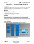
Drigmorn3 User Manual
Issue – 1.0
© Enterpoint Ltd. – Drigmorn3 Manual – Issue 1.0 02/03/2010
1
Kit Contents
You should receive the following items with your Drigmorn3 development kit:
1 - Drigmorn3 Board
2 - Programming Cable
3- USB lead.
Foreword
PLEASE READ THIS ENTIRE MANUAL BEFORE PLUGGING IN
OR POWERING UP YOUR DRIGMORN3 BOARD.
PLEASE TAKE SPECIAL NOTE OF THE WARNINGS WITHIN
THIS MANUAL.
Trademarks
Spartan-6, ISE, Webpack, EDK, COREGEN, Xilinx are the registered trademarks of Xilinx Inc,
San Jose, California, US.
Drigmorn3 is a trademark of Enterpoint Ltd.
© Enterpoint Ltd. – Drigmorn3 Manual – Issue 1.0 02/03/2010
2
Contents
Kit Contents
Foreword
Trademarks
Drigmorn3 Board
Introduction
Getting Started
FPGA
SPI FLASH
DDR3 MEMORY
DIL HEADERS
USB
ETHERNET
TOP IDC HEADER
LCD DISPLAY
LEDS
REAL TIME CLOCK
POWER MONITOR/MASTER RESET
OSCILLATOR
SWITCHES
SERIAL EEPROM
MICRO SD CARD HOLDER
ACCELEROMETER
PS2
INPUT POWER CONNECTIONS
POWER REGULATORS
PROGRAMMING DRIGMORN3
MECHANICAL
Medical and Safety Critical Use
Warranty
Support
© Enterpoint Ltd. – Drigmorn3 Manual – Issue 1.0 02/03/2010
2
2
2
4
5
6
8
9
10
12
14
16
18
19
21
23
25
26
27
28
29
30
31
33
34
36
39
41
41
41
3
Drigmorn 3
© Enterpoint Ltd. – Drigmorn3 Manual – Issue 1.0 02/03/2010
4
Introduction
Welcome to your Drigmorn3 board. Drigmorn3 is Enterpoint’s first Spartan-6
development board. It offers a highly powerful, flexible and low cost approach to
prototyping FPGA and System designs.
The aim of this manual is to assist in using the main features of Drigmorn3.
There are features that are beyond the scope of the manual. Should you need to use
these features then please email [email protected] for detailed instructions.
Drigmorn3 currently comes with a XC6SLX16-2CSG324CES Spartan-6. Other
variants may be offered at a later date or as an OEM product. Spartan-6 parts up to
XC6SLX45 can be fitted to this board. Please contact out us on
[email protected] should you need further information.
Drigmorn3 is supported by a wide range of add-on modules. Some examples of these
include:
ADC 7927 MODULE
LED DOT MATRIX MODULE
BUTTONS/SWITCHES/SATA/MEMORY MODULE
RS232 AND RS485 HEADER MODULES
DP83816 ETHERNET MODULE
SD CARD MODULE
DDR2 MODULE
IDE/5V TOLERANT CPLD MODULE
USB MODULE
D/A CONVERTER MODULE
ADV70202 MODULE
We can also offer custom DIL Header modules should you require a function not
covered by our current range of modules. Typical turn around for this service is 6-8
weeks depending upon quantity ordered and availability of components.
© Enterpoint Ltd. – Drigmorn3 Manual – Issue 1.0 02/03/2010
5
Getting Started
20 IOs on IDC
HEADER
4 WAY DIP
SWITCH
2X16 LCD
DISPLAY
SPARTAN-6
FPGA
5V PICK UP
HEADER
2 PUSH
BUTTON
SWITCHES
13 LEDs
REAL TIME
CLOCK
DN1306EN
ETHERNET
INTERFACE
1GBIT DDR3
MEMORY
16KBIT
EEPROM
USB
INTERFACE
128M
FLASH
MEMORY
BATTERY HOLDER
FOR REAL TIME
CLOCK
DIL HEADERS
WITH FORTY 5V
TOLERANT IO
MICRO SDCARD
HOLDER (ON BACK
OF BOARD
JTAG
CONNECTOR
RJ45
CONNECTOR
ACCELEROMETER
MINI USB
CONNECTOR
TWO PS2
PORTS
Your Drigmorn3 will be supplied un-programmed. Unless you have bought an OEM
product your board will be supplied with either a Prog2 parallel port programming
cable or a Prog3 USB port programming cable.
The Spartan-6 FPGA on board is supported by the free ISE Webpack 11.1 SP4, or
later, available from Xilinx providing all the tools to enter and build a design. Using
this tool in conjunction with your supplied programming cable you will also be able
to program the Spartan-6, and the supporting SPI Flash, that are on Drigmorn3.
© Enterpoint Ltd. – Drigmorn3 Manual – Issue 1.0 02/03/2010
6
ISE Webpack can be obtained directly from the Xilinx website at
http://www.xilinx.com/ise. Registration will be necessary to complete the download.
Once you have obtained your ISE Webpack tools:
(1) Connect your programming cable to the board and your PC hosting the Xilinx
software.
(2) Connect the Drigmorn3 board to either a USB connector of a PC, a USB power
supply or some other 5V source plugged into the 5V pickup socket using the
supplied USB lead. Note that some Laptops and desktop computer USB ports
have a current limit of 100mA. Drigmorn3 can exceed this in some circumstances
and should you have a problem a powered USB hub or external mains to USB
adaptor are recommended solutions.
(3) If using an external power brick switch on your power source.
© Enterpoint Ltd. – Drigmorn3 Manual – Issue 1.0 02/03/2010
7
FPGA
SPARTAN-6
FPGA
Drigmorn3 supports Spartan-6 devices in the CSG324 package. Drigmorn3 is
normally available with commercial grade -2 speed devices fitted in the XC6SLX16
size. Should you have an application that needs industrial, faster speed grades, or
bigger parts please contact sales for a quote at [email protected].
© Enterpoint Ltd. – Drigmorn3 Manual – Issue 1.0 02/03/2010
8
SPI FLASH MEMORY
128M FLASH
MEMORY
The M25P128 SPI flash memory device configures the FPGA when it is powered
providing a suitable bitstream is programmed into the device. The M25P128 has a
capacity of 128Mbits with a single configuration bitstream for Drigmorn3 taking
between 3.6Mbits (LX16) and 11.4Mbits (LX45). Any remaining space can be used
for alternative configurations or code and data storage.
After configuration the SPI Flash can be accessed via the following pins of the
FPGA:
M25P128
FUNCTION
CCLK
MOSI
WRITE
DIN
CSO_B
FPGA PIN
R15
T13
T8
R13
V3
The HOLD pin of this memory device is permanently connected to 3.3V.
© Enterpoint Ltd. – Drigmorn3 Manual – Issue 1.0 02/03/2010
9
DDR3 MEMORY
1GBIT DDR3
Drigmorn3 has a 1GBIT DDR3 Micron MT41J64M16LA device as standard. This
device is organised as 8 Meg x 16 x 8 banks. This device is supported by the hard
core memory controller that is in the Spartan-6 FPGA. To add this core to your
design the COREGEN tool, part of the ISE suite, will generate implementation
templates in VHDL or Verilog for the configuration that you want to use. More
details on the memory controller can be found in the user guide
http://www.xilinx.com/support/documentation/user_guides/ug388.pdf.
The DDR3 has 12 address lines and 16 data lines to address all the available memory,
which can be accessed at speeds of 1.87ns. More details of the DDR3 can be found in
http://download.micron.com/pdf/datasheets/dram/ddr3/1Gb_DDR3_SDRAM.pdf.
For OEM applications we can fit bigger DDR3 parts subject to limitations of the
memory controller.
© Enterpoint Ltd. – Drigmorn3 Manual – Issue 1.0 02/03/2010
10
The DDR3 site has the following connections to the FPGA:
DDR3 FUNCTION
DDR_A0
DDR_A1
DDR_A2
DDR_A3
DDR_A4
DDR_A5
DDR_A6
DDR_A7
DDR_A8
DDR_A9
DDR_A10
DDR_A11
DDR_A12
DDR_A13
DDR_A14
DDR_A15
DDR_BA0
DDR_BA1
DDR_BA2
DDR_CS_N
DDR_RAS_N
DDR_WE_N
DDR_DQ0
DDR_DQ1
DDR_DQ2
FPGA PIN
H15
H16
F18
J13
E18
L12
L13
F17
H12
G13
E16
G14
D18
C17
C18
F15
H13
H14
K13
P16
K15
K12
M16
M18
L17
DDR3 FUNCTION
DDR_DQ3
DDR_DQ4
DDR_DQ5
DDR_DQ6
DDR_DQ7
DDR_DQ8
DDR_DQ9
DDR_DQ10
DDR_DQ11
DDR_DQ12
DDR_DQ13
DDR_DQ14
DDR_DQ15
DDR_LDM
DDR_LDQS
DDR_LDQS_N
DDR_UDM
DDR_UDQS
DDR_UDQS_N
DDR_ODT
DDR_CAS_N
DDR_RESET_N
DDR_CKE
DDR_CLK_N
DDR_CLK
FPGA PIN
L18
H17
H18
J16
J18
N17
N18
P17
P18
T17
T18
U17
U18
L15
K17
K18
L15
N15
N16
K14
K16
F14
D17
G18
G16
The signals shown shaded in yellow are terminated using suitable arrangements of
resistors.
Three timing loops have also been implemented on the PCB and connected to the
FPGA to facilitate compensation for temperature and timing delays where necessary.
The pins used are shown below:
LOOP
1
2
3
FPGA
PIN1
M11
T9
N8
FPGA
PIN2
N11
V9
M8
© Enterpoint Ltd. – Drigmorn3 Manual – Issue 1.0 02/03/2010
11
DIL HEADERS
LEFT COLUMNS
OUTER PINS
S6 INNER
ROW FUNCTION PIN PINS
1
IO_L62P_2 R3
0V
2
IO_L62N_2 T3
0V
3
IO_L63P_2 T4
0V
4
IO_L63N_2 V4
0V
5
IO_L47P_2 N6
0V
6
IO_L47N_2 P7
0V
7
IO_L46P_2 R7
0V
8
IO_L46N_2 T7
0V
9
IO_L64P_2 N5
0V
10
IO_L64N_2 P6
0V
11
IO_L49P_2 U5
0V
12
IO_L49N_2 V5
0V
13
IO_L14P_2 U13
0V
14
IO_L14N_2 V13
0V
15
IO_L12P_2 T14
0V
16
IO_L12N_2 V14
0V
17
IO_L5P_2 U15
0V
18
IO_L5N_2 V15
0V
19
IO_L2P_2 U16
0V
20
IO_L2N_2 V16
0V
RIGHT COLUMNS
OUTER PINS
INNER
PINS FUNCTION PIN
3.3V
IO_L2P_0
B2
3.3V
IO_L2N_0 A2
3.3V
IO_L3P_0
D6
3.3V
IO_L3N_0 C6
3.3V
IO_L4P_0
B3
3.3V
IO_L4N_0 A3
3.3V
IO_L5P_0
B4
3.3V
IO_L5N_0 A4
3.3V
IO_L11P_0 D8
3.3V
IO_L11N_0 C8
3.3V
IO_L10P_0 C7
3.3V
IO_L10N_0 A7
3.3V
IO_L33P_0 B8
3.3V
IO_L33N_0 A8
3.3V
IO_L32P_0 G8
3.3V
IO_L32N_0 F8
3.3V
IO_L35P_0 B9
3.3V
IO_L35N_0 A9
3.3V
IO_L34P_0 D9
3.3V
IO_L34N_0 C9
The DIL Headers provide a simple mechanical and electrical interface for add-on
modules. There are twenty I/O on each side of the DIL Header giving a total of 40
I/O available. Each of these I/O pins is protected by bus switch technology to
facilitate 5V tolerance on all of these pins. Bus switch technology has a minimal
effect on I/O timing with propagation times of less than 250ps through these devices.
The DIL Headers can also support up 20 pairs of LVDS signalling when not used for
add-on modules. The Spartan-6 FPGA can terminate any of these pairs. LVDS
termination on individual signal pairs is a programmable option that can be set in
build constraints for the FPGA when using the ISE toolset. The LVDS pairs are
shown in the table above along with Spartan-6 pin numbers.
© Enterpoint Ltd. – Drigmorn3 Manual – Issue 1.0 02/03/2010
12
The DIL Headers support the use of add-on modules enhancing the capabilities of
your Drigmorn3 board. Enterpoint has a wide range of modules suitable for the DIL
Header. Details at http://www.enterpoint.co.uk/moelbryn/modules/modules.html. We
can also offer custom design modules should our standard range not cover your
requirement. The DIL Headers will also support the use of crude prototype circuits
using stripboard or other prototype materials.
The DIL Header connectors are arranged on a standard 0.1inch (2.54mm) pitch. The
horizontal pitch of the DIL Headers is 1.6 inches between the outer rows of the
headers. The inner pins of the header form continuous power strips allowing a range
of modules to be used together in one header subject to sufficient pins being
available. The right hand side header has an inner column of 3.3V pins. The LHS
header has an inner column of DGND (0V).
© Enterpoint Ltd. – Drigmorn3 Manual – Issue 1.0 02/03/2010
13
USB
FT232R USB
DEVICE
USB SOCKET
The USB interface on the Drigmorn 3 is achieved using an FT232R USB to serial
UART interface. The datasheet and drivers for this device are available from
http://www.ftdichip.com. When appropriate drivers are installed the Drigmorn3 USB
port should be detected as a serial port. Alternative data optimised drivers are also
available from FTDI.
The FT232R is connected to the Spartan-6 and provided a simple UART, or other
converter, is implemented then the data sent over the USB serial port can be used
either as control and/or data information. This allows a host computer to act in a
number of ways including system control and data storage functions.
The FT232R can also supply a clock to the Spartan-6 FPGA using CBUS4 I/O. This
I/O can be programmed by tools available from FTDI to output different frequencies
or other functions. The FT232R can provide clock frequencies of 6/12/24/48MHz.
© Enterpoint Ltd. – Drigmorn3 Manual – Issue 1.0 02/03/2010
14
The connections between the USB device and the FPGA are shown below:
FT232R
CBUS4
CTS#
DCD#
DSR#
RI#
RTS#
DTR#
TXD
RXD
FPGA PIN
C10
B12
A12
E11
B11
F10
F11
G11
A11
The FT232R connections CBUS0 to CBUS3 are routed via a resistor array site
(resistor array not fitted) to the JTAG connector for future use in reconfiguring the
FPGA via a USB interface, a scenario which is theoretically possible but not so far
established. These connections, were the resistor array to be fitted, would be as
shown below:
FT232R
CBUS0
CBUS1
CBUS2
CBUS3
JTAG
SIGNAL
TDO
TDI
TMS
TCK
© Enterpoint Ltd. – Drigmorn3 Manual – Issue 1.0 02/03/2010
15
ETHERNET
KSZ8851
ETHERNET
DEVICE
RJ45 CONNECTOR
Drigmorn3 Ethernet connector showing dimensions
The Drigmorn3 Ethernet interface uses a Micrel KSZ8851SNL device. The KSZ8851
incorporates a Fast Ethernet MAC/PHY with an 8/16/32 bit generic host processor
interface and SPI interface. All datasheets and support documentation can be found
on Micrel’s website www.micrel.com.
© Enterpoint Ltd. – Drigmorn3 Manual – Issue 1.0 02/03/2010
16
The connections between the KSZ8851 and the FPGA are as shown below:
KSZ8851
PME
INTRN
SI
SO
CSN
SCLK
RSTN
X1
FPGA PIN
V10
T10
M10
V11
P11
N9
U11
R10
Pin X1 of the KSZ8851SNL has been routed to the FPGA so that the Ethernet Clock
frequency (25MHz) can be provided by the FPGA. You will need to implement this
in any designs for the Ethernet to work.
The KSZ8851 has been provided with an AT93C46E EEPROM as required by the
specification. It communicates to the ‘outside world’ via an RJ45 connector (Pulse
J3006G21D) which has green and yellow LEDs which indicate whether a connection
to an Ethernet hub is present.
MAC ADDRESS DEVICES
The Drigmorn3 has a MAC address device fitted which assigns the boards a unique
identity number. The device used is a MAXIM DS2502-E48+, of which further
details can be found on http://ww.maxim-ic.com. There are two sites on the
Drigmorn3 for DS2502-E48+ devices, one is a 6 pin TSOC6 site, the other is a 3 pin
TO-92 site. Normally only one of these devices is fitted (unless specifically requested
by the customer). The 6 pin device is defined as Mac Address 1 and the 3 pin device
is defined as Mac Address 2. It should be straightforward to determine which of these
2 devices is fitted on your board. The connections to the FPGA are shown below:
The table below shows the location of the MAC address devices on the Drigmorn 3.
MAC ADDRESS DEVICE
FPGA PIN
6 PIN TSOC6 DEVICE (MAC ADDRESS 1)
R8
3 PIN TO-92 DEVICE (MAC ADDRESS 2)
V10
© Enterpoint Ltd. – Drigmorn3 Manual – Issue 1.0 02/03/2010
17
TOP IDC HEADER
IDC HEADER
At the top of the Drigmorn3 there is a 40 way IDC connector. This has 20 IO
connections to the FPGA and 20 DGND(0V) connections. The IOs are wired directly
to the Spartan-6 FPGA so signal voltage to these pins should not exceed 3.3V.
The connections between the IDC connector and the FPGA are shown below. Pin 1
of the IDC header is defined as the pin on the left of the lower row of pins, as viewed
from the front of the board.
IDC PIN
1
3
5
7
9
11
13
15
17
19
FPGA PIN
L7
L5
L4
L3
L1
L2
K1
K2
K3
K4
21
23
25
27
29
31
33
35
37
39
© Enterpoint Ltd. – Drigmorn3 Manual – Issue 1.0 02/03/2010
K5
J3
J1
H3
H1
H2
G1
G3
H4
K6
18
LCD DISPLAY
LCD DISPLAY
The standard Drigmorn 3 LCD display is an LCM-S01602DTR/M display, which is
16x2 alpha-numerical display with a Hitachi HD44780 compatible chipset. More
information on this at http://www.lumex.com/specs/LCM-S01602DTR%20M.pdf.
For OEM applications this LCD can be replaced by a 2x17 IDC header allowing
remote location of the LCD or even reuse of the interface for other I/O functions. For
these applications the 8 data signals are passed through bus switches giving 5V
tolerance. The remaining signals of this interface are not protected for 5V operation
and should only be used with voltages less than 3.3V.
For OEM applications we can offer other display solutions with graphic, colour LCD
and OLED options. Contact us for specific requirements.
© Enterpoint Ltd. – Drigmorn3 Manual – Issue 1.0 02/03/2010
19
The IO pins used for the display are shown in the table below:
FUNCTION
Backlight
ON
D7
D6
D5
D4
D3
D2
D1
D0
EN
R/W
RS
FPGA PIN
C1
U1
U2
M5
L6
P3
P4
N3
N4
P2
T2
T1
© Enterpoint Ltd. – Drigmorn3 Manual – Issue 1.0 02/03/2010
20
LEDS
LED7
LED6
LED5
LED4
LED3
LED2
LED1
LED13
LED12
LED11
LED10
LED9
LED8
Drigmorn3 has 13 LEDs. There is a single red LED in the centre of the board just
above the FPGA, and 12 LEDs arranged into 4 blocks of three, one of each block
being red, orange and green. This is to enable users to simulate a traffic light
sequence. The LEDS will turn on dimly when power is applied to the board. The
relevant IO pin for an LED needs to be asserted high to ensure the specific LED turns
on.
Users may wish to visit out TechiTips section of the Enterpoint engineering website
for tutorial and lab materials using Traffic Light LEDs. Our Techitips are located at
http://www.enterpoint.co.uk/techitips/techitips.html.
© Enterpoint Ltd. – Drigmorn3 Manual – Issue 1.0 02/03/2010
21
The LEDS are connected to the FPGA as indicated below:
LED
1
2
3
4
5
6
7
8
9
10
11
12
13
FPGA PIN
U7
V7
N7
P8
T6
V6
M3
E8
E7
E6
F7
A5
C5
COLOUR
RED
ORANGE
GREEN
GREEN
ORANGE
RED
RED (SINGLE)
RED
ORANGE
GREEN
GREEN
ORANGE
RED
© Enterpoint Ltd. – Drigmorn3 Manual – Issue 1.0 02/03/2010
22
REAL TIME CLOCK
REAL TIME
CLOCK
DN1306EN
BATTERY HOLDER
FOR REAL TIME
CLOCK
The Drigmorn3 has a Maxim DS1306EN+ Serial Alarm Real time clock device with
a 32.768KHz crystal. Further information and datasheets for this device can be found
on http://ww.maxim-ic.com.
The DS1306EN+ can provide a 32.768KHz clock, timed interrupts, and data storage
features. Please consult the device datasheet for more details.
The DS1306EN+ is supported by a battery holder that can take CR1220/1225 battery
types. We do not normally supply the battery to avoid shipping issues with batteries.
© Enterpoint Ltd. – Drigmorn3 Manual – Issue 1.0 02/03/2010
23
The connections between the Real Time Clock device and the FPGA are shown
below:
DS1306EN+
FPGA PIN
IHZ
J7
SDI
G6
INT1
C2
INT0#
D3
32KHZ
E4
SDO
F5
SCLK
F6
CE
H7
© Enterpoint Ltd. – Drigmorn3 Manual – Issue 1.0 02/03/2010
24
POWER MONITOR AND MASTER RESET
The Drigmorn3 has a voltage monitor which monitors the 3.3V, 1.2V and 0.75V
supplies within the board. If any of these voltages are missing the reset signal is held
active. Connector J2 (found at the very top left of the board) provides a manual reset
facility. Placing a jumper between the centre pin of J2 and the leftmost pin (pin 1,
0V) will cause an active reset signal. This header can also be used for an external
system reset with a remote switch or relay wired across the pins.
© Enterpoint Ltd. – Drigmorn3 Manual – Issue 1.0 02/03/2010
25
OSCILLATOR
OSCILLATOR
The main oscillator on the Drigmorn3 is an ASEM 25MHz or 50MHz oscillator. The
50 MHz is fitted for early boards using CES grade silicon. Boards with full C grade
silicon will have a 25MHz oscillator. The oscillator is situated as shown in and is
connected the FPGA on PIN D11.
The Spartan-6 has PLLs and DCMs to produce multiples, divisions and phases of the
clock for specific application requirements. Please consult the Spartan-6 datasheet
available from the Xilinx website at http://www.xilinx.com if multiple clock signals
are required.
© Enterpoint Ltd. – Drigmorn3 Manual – Issue 1.0 02/03/2010
26
SWITCHES
DIP SW BIT0
DIP SW BIT3
PUSH BUTTON
SWITCH SW3
PUSH BUTTON
SWITCH SW1
The Drigmorn3 has two push button switches and one 4 way DIP switch. To use
these switches it is necessary to set the IO pins connected to the switches to have a
pull up resistor in the FPGA. This is set in FPGA constraints file. Any switches
pressed, or made, will then give a LOW signal at the FPGA otherwise a HIGH is
seen. The two push button switches are connected to the following IO pins.
SW1 (LEFT)
V12
SW3 (RIGHT)
E12
The four DIP switch bits are connected to the following IO pins.
BIT0
H5
BIT1
F3
BIT2
D2
© Enterpoint Ltd. – Drigmorn3 Manual – Issue 1.0 02/03/2010
BIT3
D1
27
16k SERIAL EEPROM
16K SERIAL
EEPROM
The Drigmorn3 has an Atmel AT24C16 EEPROM device, which use a simple
Parallel address and single serial data line and clock. There is also a write protect line
which can be used to electronically safeguard the information contained in the device.
This serial memory has 2048 words of 8 bits and employs a byte or page
programming system. It can run at speeds up to 400 kHz. The EEPROM has the
following connections to the FPGA:
EEPROM PIN
SDA
SCL
WP
FPGA PIN
P1
N2
N1
The address pins on this device are wired to DGND(0V).
© Enterpoint Ltd. – Drigmorn3 Manual – Issue 1.0 02/03/2010
28
MICRO SD CARD HOLDER
MICRO SDCARD
SOCKET (ON
BACK OF BOARD)
Further access to data can be achieved using the Micro SD Card Socket which is
situated on the back of the Drigmorn 3 board. To use this socket in a design you may
need to obtain a license from the SD Association at http://www.sdcard.org/home/.
The connections between the Micro SD Card Socket and the FPGA are shown below:
SDCARD SOCKET
DATA 0
DATA 1
DATA 2
DATA 3
CMD
CLK
POWER_ON_N
FPGA PIN
F2
E1
J6
H6
F4
E3
F1
The POWER_ON_N pin must be set LOW for power to be supplied to the SDCARD
Reader.
© Enterpoint Ltd. – Drigmorn3 Manual – Issue 1.0 02/03/2010
29
ACCELEROMETER
ACCELEROMETER
The Drigmorn 3 has an MMA7455L 3 axis accelerometer which has 3 sensitivity
ranges: ±2g, ±4g and ±8g. Typical applications for this device are tilt and motion
sensing, freefall detection and shock and vibration detection and these types of
devices are used in cell phones, anti-theft equipment, pedometers, e-compasses and
for 3d gaming. The datasheet for this accelerometer can be obtained from
www.freescale.com. This device has both SPI and I2C interfaces. The connections
between the accelerometer and the FPGA are shown below:
ACCELEROMETER
CS
INT1/DRDY
INT2
SDO
SDA/SDI/SDO
SLC/SPC
IADDR0
FPGA PIN
C13
C12
D12
A13
B14
G9
FIXED 0V
© Enterpoint Ltd. – Drigmorn3 Manual – Issue 1.0 02/03/2010
30
PS2
TWO PS2
PORTS
14mm
13mm
The Drigmorn3 has two PS2 ports which connect to the FPGA through bus switches
and hence are 5V tolerant. These can be used to connect to a keyboard and mouse or
for other user-defined functions.
© Enterpoint Ltd. – Drigmorn3 Manual – Issue 1.0 02/03/2010
31
The connections to the FPGA are shown below. Connector 1 is defined as the
connector on the left.
PS2
CONNECTOR1 PIN 1 (LEFT)
CONNECTOR1 PIN 2
CONNECTOR1 PIN 3
CONNECTOR1 PIN 5
CONNECTOR1 PIN 6
CONNECTOR1 PIN 8
CONNECTOR2 PIN 1 (RIGHT)
CONNECTOR2 PIN 2
CONNECTOR2 PIN 3
CONNECTOR2 PIN 5
CONNECTOR2 PIN 6
CONNECTOR2 PIN 8
© Enterpoint Ltd. – Drigmorn3 Manual – Issue 1.0 02/03/2010
FPGA PIN
A16
B16
Wired to 0V
Wired to 5V
C14
A15
E13
F13
Wired to 0V
Wired to 5V
D14
C15
32
POWER CONNECTIONS
ROW OF 20 0V
CONNECTIONS ON IDC
HEADER
5V PICK UP
1.2V
REGULATOR
3.3V
REGULATOR
MINI USB
CONNECTOR
COLUMN OF 20 0V
CONNECTIONS ON
LHS DILHEADER
COLUMN OF 20 3.3V
CONNECTIONS ON
RHS DILHEADER
Drigmorn3 is powered principally from the USB connector. The board should be
plugged via a cable into the USB slot of a PC, Laptop or USB hub. Some USB ports
may not be able to supply greater than 100mA and either a powered USB hub or a
mains wall brick is suggested for these cases. Whatever power supply is used care
should be taken not to exceed 5.5V input as this can cause damage to the Drigmorn3.
It is also possible to power the Drigmorn3 via the 5V pickup header. Using this
feature we can offer various fit options for OEM purchasers of this board including
rear mounted headers or flying wires using this feature. The header supports two 5V
and 0V(DGND) connections. The 5V pickup header can also be used to act as a 5V
supply to daughter cards needing 5V that are mounted in the DIL Header. The photo
above shows the standard arrangement or non-OEM boards.
© Enterpoint Ltd. – Drigmorn3 Manual – Issue 1.0 02/03/2010
33
POWER REGULATORS
3.3V
REGULATOR
1.5V
REGULATOR
0.75V
REGULATOR
1.2V
REGULATOR
Drigmorn3 has four regulators supplying 3.V, 1.5V, 1.2V and 0.75V power rails.
WARNING – REGULATORS CAN BECOME HOT IN NORMAL
OPERATION ALONG WITH THE BOARDS THERMAL RELIEF. PLEASE
DO NOT TOUCH OR PLACE HIGHLY FLAMABLE MATERIALS NEAR
THESE DEVICES WHILST THE DRIGMORN3 BOARD IS IN OPERATION.
An Empirion EP5388QI regulator supplies 3.3V with a maximum current available of
800mA. This powers the FPGA general I/O, DIL Header and other devices such the
Ethernet controller and Real Time Clock.
An Empirion EP5388QI regulator supplies 1.5V with a maximum current available of
800mA. This is used for the DDR3 and related FPGA I/O.
A Micrel MIC33050 regulator supplies 1.2V with a maximum current of 600mA for
the core voltage of the FPGA .
© Enterpoint Ltd. – Drigmorn3 Manual – Issue 1.0 02/03/2010
34
A National Semiconductor LP2996 push-pull regulator produces up to 1.5A at 0.75V.
This supply is used as reference and termination voltage for the DDR3 memory and
related FPGA I/O.
© Enterpoint Ltd. – Drigmorn3 Manual – Issue 1.0 02/03/2010
35
Programming Drigmorn3
JTAG Header
The programming of the FPGA and SPI Flash parts on Drigmorn3 is achieved using
the JTAG interface. Principally it is anticipated that a JTAG connection will be used
in conjunction with Xilinx ISE software although other alternatives do exist including
self re-programming. The Spartan-6 series needs to be programmed using ISE 11 or
higher. Versions of ISE prior to 11 do not support Spartan-6. The free Webpack
version of the Xilinx tools can be used to program the Drigmorn3.
© Enterpoint Ltd. – Drigmorn3 Manual – Issue 1.0 02/03/2010
36
There is a single JTAG chain on Drigmorn3. The JTAG chain allows the
programming of the Spartan-6 and SPI Flash device.
The JTAG connector has a layout as follows (top view):
GND
NC
GND
NC
GND
TDI
GND
TDO
GND
TCK
GND
TMS
GND
3V3
Using iMPACT Boundary Scan the JTAG chain appears like this:
1. Programming the FPGA directly.
Direct JTAG programming of the Spartan-6 FPGA is volatile and the FPGA will lose
its configuration every time the board power is cycled. For sustained use of an FPGA
design programming the design into the Flash memory is recommended (see 2 and 3
below).
Direct JTAG programming using .bit files is useful for fast, temporary programming
during development of FPGA programs. Right click the icon representing the
Spartan-6 FPGA and choose ‘Assign New Configuration File’. Navigate to your .bit
file and choose ‘OPEN’. The next dialogue box will offer to add a flash memory and
you should decline. Right click the icon representing the Spartan-6 FPGA and choose
‘Program’. On the next dialogue box ensure that the ‘Verify’ box is not checked. (If it
is you should uncheck it, failure to do this will result in error messages being
displayed). Click OK. The Spartan-6 will program. This process is very quick
(typically one second)
2. Programming the SPI flash memory using Boundary Scan.
Once the SPI Flash memory has been programmed, the Spartan-6 device will
automatically load from the Flash memory at power up. Generation of suitable Flash
memory files (.mcs) can be achieved using ISE iMPACT’s Prom File Formatter.
Right click on the icon representing the Spartan-6 and choose ‘Add SPI/BPI Flash’
Navigate to your programming file (.mcs) and click OPEN. Use the next dialogue
box to select SPI flash and M25P128. Data width should be set to 1. The flash
memory should appear as shown below.
© Enterpoint Ltd. – Drigmorn3 Manual – Issue 1.0 02/03/2010
37
Right click on the icon representing the flash memory and choose program to load
your program into the device. It is recommended that options to ‘Verify’ and ‘Erase
before programming’ are chosen. Otherwise all defaults can be accepted. The
programming operation will take some time (at least 3 or 4 minutes)
© Enterpoint Ltd. – Drigmorn3 Manual – Issue 1.0 02/03/2010
38
MECHANICAL ARRANGEMENT
The Dimensions on the drawing below are millimetres (mm). All sizes quoted are
subject to manufacturing tolerances and should only be used as a general guide.
© Enterpoint Ltd. – Drigmorn3 Manual – Issue 1.0 02/03/2010
39
The heights of the components, measured from the lower surface of the board are as
follows:
Upper surface of LCD display: 12.5mm
Ethernet connector:15.3mm
USB connector: 5.5mm
PS2 connectors 14.7mm
Micro SD card holder, measured from top surface of PCB to bottom of
SD card holder: 2.6mm
The PCB is 1.6mm thick
Mechanical Arrangement of DIL headers
The socket pins on the DIL headers and 5V pickup are arranged on a 2.45mm
(0.1inch) pitch
© Enterpoint Ltd. – Drigmorn3 Manual – Issue 1.0 02/03/2010
40
Medical and Safety Critical Use
Drigmorn3 boards are not authorised for the use in, or use in the design of, medical or
other safety critical systems without the express written person of the Board of
Enterpoint. If such use is allowed the said use will be entirely the responsibility of the
user. Enterpoint Ltd will accepts no liability for any failure or defect of the
Drigmorn3 board, or its design, when it is used in any medical or safety critical
application.
Warranty
Drigmorn3 comes with a 90 day return to base warranty. Do not attempt to solder
connections to the Drigmorn3. Enterpoint reserves the right not honour a warranty if
the failure is due to soldering or other maltreatment of the Drigmorn3 board.
Outside warranty Enterpoint offers a fixed price repair or replacement service. We
reserve the right not to offer this service where a Drigmorn3 has been maltreated or
otherwise deliberately damaged. Please contact support if you need to use this
service.
Other specialised warranty programs can be offered to users of multiple Enterpoint
products. Please contact sales on [email protected] if you are interested in
these types of warranty,
Support
Please check our FAQ page for this product first before contacting support. FAQ is
located at http://www.enterpoint.co.uk/drigmorn/drigmorn3_faq.html. Telephone and
email support is offered during normal United Kingdom working hours (GMT or
GMT + 1) 9.00am to 5.00pm.
Telephone - +44 (0) 121 288 3945
Email
- [email protected]
© Enterpoint Ltd. – Drigmorn3 Manual – Issue 1.0 02/03/2010
41