1
EE 101 Lab 1 - Sound the Alarm
5 Procedure
1. Given the description of the alarm system in section 3, design a logic circuit to
implement the alarm system. Use only inverters and the 2-input AND and OR
gates (no NOR and NAND for now). For inputs and outputs use the following
mapping:
Logical
Input/Output
N
X
W
D
G
A
Trainer Board I/O Device
SW1
SW4
PB1
PB2
PB3
LED5
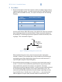
Since the push buttons (PB1-PB3) output a 1 by default this means the window,
door, and garage values are secure by default. When we press the buttons it
will produce a ‘0’ indicating someone has opened or broken the window, door
or garage. This is reiterated in Figure 1.
Vdd
PB1-PB3 =
W, D, or G
‘1’ (secure)
by default
GND
(Vss)
Figure 1 - PB outputs producing the W, D, and G values
When implementing your circuit, note that you only have 2-input gates
available. However, you should be able to easily handle this shortcoming by
manipulating your design slightly (think about how you could construct a 3input AND gate using two 2-input AND gates.)
2. Once you have wired your design, it is now time to test it and make sure it is
correct. To test this circuit exhaustively would require trying every possible
input combination and ensure the output is as expected. How many
combinations would this approach require? Instead, use your understanding of
the intended logic design to devise a list of input combinations (a.k.a. test
vectors) that provide high satisfaction that your design is operating correctly
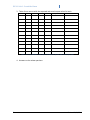
(e.g. {N,X,W,D,G}=>A = {0,0,0,0,1}=>0, {1,0,0,1,0}=>1,…). Use the attached
table on page 4 to list your (near) minimal number of combinations, the
2
Last Revised: 8/31/2011