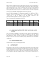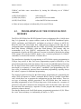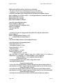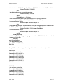
1
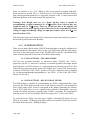
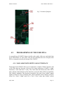
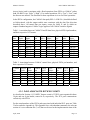
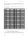
User’s Manual
Model ULM52C
Universal Logical Module
For CAMAC Systems
JTEC Instruments
32 Thompson Rd.
Rochester, NY, USA
Tel: (585)-334-7215
http://www.jtec-instruments.com
Information furnished by JTEC Instruments (JTEC) is believed to be accurate and reliable. However,
no responsibility is assumed by JTEC for its use, nor for any infringements of patents or other rights
of third parties, which may result from its use. No license is granted by implication or otherwise under
any patent or patents rights of JTEC. JTEC reserves the right to change specifications at any time
without notice.
Copyright 2004 by JTEC
Manual #: mdo-ULM52C-MAN-001.1
April 2004
Manual: ULM52C
mdo-ULM52C-MAN-001.0
TABLE OF CONTENTS
1.
OVERVIEW ............................................................................................................................ 2
1.1.
1.2.
2.
3.
SUMMARY OF FEATURES ........................................................................................................ 2
POSSIBLE APPLICATIONS ........................................................................................................ 2
SPECIFICATIONS .................................................................................................................. 3
ARCHITECTURE ................................................................................................................... 4
3.1. FIELD PROGRAMMABLE GATE ARRAY................................................................................ 4
3.1.1.
FLASH MEMORY................................................................................................................. 5
3.1.2.
UTILITY CPLD ..................................................................................................................... 5
3.1.3.
ECL PORTS ........................................................................................................................... 5
3.1.4.
USER LEDs............................................................................................................................ 5
4.
OPERATING INSTRUCTIONS ............................................................................................. 7
4.1. HARDWARE SETUP.................................................................................................................... 7
4.1.1.
IMPORTANT RULES ........................................................................................................... 7
4.1.2.
CONFIGURING ECL PORTS............................................................................................... 8
4.1.3.
JUMPER SETTINGS ........................................................................................................... 10
4.2. PROGRAMMING OF THE USER FPGA................................................................................... 11
4.2.1.
PADS ASSOCIATED WITH CAMAC INTERFACE ........................................................ 11
4.2.2.
PADS ASSOCIATED WITH ECL PORTS ......................................................................... 12
4.2.3.
PADS ASSOCIATED WITH USER LEDs ......................................................................... 13
4.2.4.
PADS ASSOCIATED WITH USER CLOCK AND CLOCK ENABLE............................. 14
4.2.5.
CONFIGURING FPGA........................................................................................................ 14
4.3. PROGRAMMING OF THE CONFIGURATION MEMORY .................................................... 15
5.
APPENDICES........................................................................................................................ 19
5.1.
5.2.
USER CONSTRAINTS FILE, UCF ............................................................................................ 19
SUMMARY OF SYSTEM CAMAC COMMANDS................................................................... 21
April, 2004
Page 1
Manual: ULM52C
mdo-ULM52C-MAN-001.0
JTEC Model ULM52C
Universal Logical Module
1. OVERVIEW
JTEC Model ULM52C is a highly versatile, general-purpose, programmable
universal logical module for use in CAMAC-based systems. By design, it can
communicate with external devices via 52, front-panel ECL ports, which can
be configured in quartets either as inputs or outputs. The ECL ports are
mapped onto the ports of the user FPGA, an XC2S200 by Xilinx. On the other
end, ULM52C communicates with computers via the CAMAC bus, utilizing
full set of CAMAC commands and a 24-bit data bus. Furthermore, ULM52C
features an on-board 4 MByte EEPROM or flash memory allowing one to
store up to two FPGA configuration files.
Few digital applications are outside of ULM52C range.
1.1.
•
•
•
•
•
SUMMARY OF FEATURES
52 programmable front-panel ECL ports, configurable in quartets as either
inputs or outputs, organized in three 34-pin and one 8-pin headers. Three
ports can be configured as external clock ports of the FPGA.
One user-programmable FPGA, XC2S200-6PQ208C by Xilinx, Inc.
One 4-MByte programmable erasable read-only memory holding up to two
FPGA configuration files.o
Six front-panel LEDs, mapped onto ports of the user FPGA.
FastCamac ready.
1.2.
•
•
•
•
•
•
POSSIBLE APPLICATIONS
Intelligent Data Buffer
Scalers, Prescalers, Coincidence Registers, Time Stampers
Multilevel Trigger Logics
Digital Delay and Gate Generators
Detector Readout Processor
Histogramming Memory
Due to the ultimate parallelism of an FPGA, ULM52C can be programmed to perform
multiple functions simultaneously, whether mutually related or unrelated. For example,
April, 2004
Page 2
Manual: ULM52C
mdo-ULM52C-MAN-001.0
part of ULM52C may be programmed to execute trigger logic, wile other parts serving as
blocks of gated and non-gated scalers, digital delay and gate generators, coincidence
registers, etc.
2. SPECIFICATIONS
Formfactor: Single-width CAMAC.
PC Board: 4-layer, double-sided mixed surface-mount and through-hole.
CAMAC Connector: Standard CAMAC card-edge connector with gold-plated fingers.
ECL Ports: 52, mapped onto the pins of the user FPGA.
LEDs: Six user-programmable LEDs, controlled by the FPGA configuration.
Clocks: One 100 MHz
External FPGA Clock Inputs: Three, rated at 110 MHz.
FPGA: XC2S200-6PQ208 by Xilinx.
FPGA Configuration Memory: 4-MBit AT29C040A (3.3V) by Atmel.
CAMAC Data Words: 24-bit.
Front Panel: Black, anodized, with white silk-screen labeling.
Power Requirements: +6V at approximately 1. A; -6V at approximately 600 mA.
Depends on the user application.
April, 2004
Page 3
Manual: ULM52C
mdo-ULM52C-MAN-001.0
3. ARCHITECTURE
Block diagram of ULM52C is shown in Fig. 1. As seen in this figure, the user FPGA, an
XC2S200 by Xilinx, has exclusive control of ECL ports and user LEDs. It connects to the
CAMAC bus via a block of transceivers and buffers, which allow one to implement a
complete CAMAC interface. A utility CPLD controls the direction of data flow through
the transceivers according to standard rules of CAMAC. It allows one to program the onboard flash memory with the FPGA configuration file and at the boot time of the FPGA,
it serializes the 8-bit flash memory words into a stream of single bits presented to the
FPGA.
Fig. 1. Block-diagram of ULM52C.
3.1.
FIELD PROGRAMMABLE GATE ARRAY
The desired logical operations of ULM52C are to be programmed by the user into a
Xilinx XC2S200-6PQ208C field programmable gate array chip (FPGA). Any logic that
can be implemented as synchronous state machine or combinatorial equation may be
programmed, subject only to the availability of resources of the XC2S200 chip, which are
quite vast. These resources include, among other things:
April, 2004
Page 4
Manual: ULM52C
(i)
(ii)
(iii)
(iv)
(v)
(vi)
mdo-ULM52C-MAN-001.0
5,292 logic cells,
200,000 system gates,
75,264 bits of distributed RAM,
56kBits of block RAM,
Clock management with 4 DLLs, and
Fast Carry Logic.
The FPGA is clocked at 100 MHz from an on-board clock, but can be also clocked
externally via one of three special ECL ports at rates of up to 110 MHz. The on-board
clock can be disabled by the FPGA firmware.
3.1.1. FLASH MEMORY
To provide for the storage of the FPGA configuration data, ULM52C is equipped with
one 4 MBit Programmable Erasable Read-Only Memory (Flash Memory), an ATMEL
AT29CC040A. The size of this memory is sufficient to accommodate up to two
XC2S200 configuration files, one of which serves as a default boot configuration. The
Flash Memory can be reprogrammed in system via CAMAC interface. The chip is
socketed and is rated for 10,000 programming cycles and 20-year data retention.
3.1.2. UTILITY CPLD
To provide for the capability of in-system programming of the flash memory, ULM52C
is equipped with a Complex Programmable Logical Device (CPLD), an XC95144XL by
Xilinx. During the FPGA boot process, this CPLD converts 8-bit data words of the Flash
Memory into a stream of configuration bits presented to the FPGA. Furthermore, through
this utility CPLD, one can select the boot sector of the FPGA, overriding the setting of
the boot selection jumper. It has also control over the reset (PRGM) pin of the FPGA,
allowing one for a “warm” reboot of the FPGA.
3.1.3. ECL PORTS
ULM52C is equipped with 52 ECL ports organized in three 34-pin and one 8-pin header.
The ports are controlled exclusively by the FPGA and can be configured in quartets as
either inputs or outputs, but always unidirectional. Three ECL ports serve special role, as
they are associated with clock inputs GCK0, GCK1, and GCK2 of the FPGA. As such
they can serve as inputs for external clock signals to the FPGA. These three ports connect
also to standard I/O pads of the FPGA and, hence, can be used also as normal ECL ports.
3.1.4. USER LEDs
ULM52C is equipped with six front-panel light-emitting diodes (LED), all controlled by
the user configuration of the FPGA. Every LED is driven by a pulse-length extender,
such that even short, 20ns-long pulses, sent by the FPGA, produce robust flashes, while
April, 2004
Page 5
Manual: ULM52C
mdo-ULM52C-MAN-001.0
long pulses or DC levels are passed to the LED unaltered. For an unconfigured FPGA, all
LEDs are on and, hence, these LEDs serve as status indicators of the FPGA booting.
April, 2004
Page 6
Manual: ULM52C
mdo-ULM52C-MAN-001.0
4. OPERATING INSTRUCTIONS
Successful operation of ULM52C requires its proper hardware setup and configuring of
its user FPGA.
4.1.
HARDWARE SETUP
The hardware setup of ULM52C includes (i) configuring its front-panel ECL ports for
operation in conjunction with the intended FPGA configuration and (ii) making sure that
the two blocks of jumpers, JP16 and JP20, controlling the boot process, are configured
properly. Furthermore, one is expected to connect respective ECL ports to external
devices with twisted-pair or flat ribbon cables. The ECL ports are configurable in quartets
either as inputs or outputs. The three ports identified by silk-screen labels (on the front
panel and on the ULM52C board) as D2-E4 play a special role as they connect
additionally via ECL-to-TTL translators (MC10125) to clock inputs (GCK0-GCK2) of
the FPGA.
4.1.1. IMPORTANT RULES
Improper configuring of ECL ports may result in the unit not functioning properly.
Therefore, care should be taken to correctly identify and populate the sockets with
translator ICs. When not sure, please consult JTEC Support service.
Rule # 1: Only one translator IC (either input or output) is allowed for any single
port. Which, in practical terms, means that in any horizontal pair of sockets at most
one should be filled.
Rule # 2: When configuring input ports (MC10125), it must be ascertained that the
corresponding ports of the FPGA are configured, indeed, as input ports and not as
output ports.
Rule # 3: ULM52C requires differential ECL inputs and will not function properly
(no damage will occur, though) with single-ended ECL signals. Which means,
among other things, that these inputs cannot be driven by an ECL bus connected to
ECL outputs of multiple external devices.
Rule # 4: When configuring output ports, make sure that the input-polarizing
resistor arrays for the particular quartets of ECL ports, are removed from their
respective sockets.
April, 2004
Page 7
Manual: ULM52C
mdo-ULM52C-MAN-001.0
4.1.2. CONFIGURING ECL PORTS
ECL-to-TTL conversion (input) and TTL-to-ECL conversion (output) is accomplished by
16-pin MC10125 and MC10124 ICs, respectively. Each converter IC is capable of
interfacing up to four differential ECL ports to respective four TTL ports of the user
FPGA. Differential inputs of these ICs are directly connected to respective pairs of pins
of front-panel headers. The headers are identified (going from top to bottom) by labels A,
B, C, and D, respectively while individual ports within a header are identified by
numbers 1 through 16 (ports A – C) or 1 through 4 (port D). It is important to note that
(as indicated on the front panel of ULM52C), port 1 of each of the five headers is
represented by the top pair of pins of the header.
As indicated by silk-screen labels printed above each of the two columns of 13 16-pin
sockets, the input translators are to be placed into sockets in the left-most column while
the output translators are to be inserted into sockets of in the right-most column. The
correspondence between the sockets and the ECL ports is indicated by silk-screen labels
printed on the left of the translator sockets.
In addition to translator ICs, proper functioning of ECL ports requires either impedancematching resistor arrays of 8 x 50Ω (input ports) or pull-down resistor arrays of 8 x 470Ω
(output ports). These two types of arrays share “Zig-Zag” sockets, with the exception of
their first (common) pins, marked by dots. The correspondence between the ECL ports
and the (10-position) rows of the “Zig-Zag” sockets is indicated by silk-screen labels
printed on both sides of these sockets.
Figure 2 illustrates placement of translator chips and resistor arrays for ECL ports A5-A8,
configured as inputs and ports A13-A16 configured as outputs. Dots indicate pins #1.
Fig. 2. Placement of ECL port components for inputs (blue) and outputs (yellow).
April, 2004
Page 8
Manual: ULM52C
mdo-ULM52C-MAN-001.0
4.1.2.1.CONFIGURING IMPEDANCE-MATCHING RESISTOR ARRAYS
FOR ECL INPUT PORTS
As noted in subsection 4.1.2 further above, to avoid reflections of incoming signals from
the ECL input ports, 8 x 50Ωresistor arrays are to be inserted into proper rows of the
“Zig-Zag” sockets. Note that each (differential) ECL input is associated with two signal
lines and that both these lines need to be terminated. Which is why for one quartet of
inputs eight terminating resistors are needed. The 8 x 50Ω arrays are to be inserted with
their common pins entering positions marked as I1 (bottom-most positions of the 5
vertical Zig-Zag sockets and left-most positions of the 2 horizontal Zig-Zag sockets).
Warning: Even though each row of a 20-pin Zig-Zag socket is capable of
accommodating a typical commercial 9 x 50Ω resistor array with ten pins, one
should use only 8 x 50Ω arrays. This is so, because the pins on the opposite end (with
respect to I1) of the Zig-Zag sockets, labeled as O1, are connected to –5.2V, to
supply pull-down voltage for output port resistor arrays (8 x 470Ω) (see also subsection 4.1.2.3).
Note that general rules for bussing of ECL input ports require that only the last port on
the bus has its terminating resistor installed.
4.1.2.2.CONFIGURING INPUT POLARIZING RESISTORS
To guarantee a default logical zero at ECL input ports that are not externally driven,
ULM52C provides sockets for respective polarizing (pull-down of complementary ECL
input line) resistor arrays. These sockets are located left to the input translator sockets
and are associated directly with the adjacent socket. This association is also reflected in
the silk-screen label printed next to the socket. Position of the pin 1 (common) is in this
case indicated by the “cut corner” of the silk-screen socket outline (top-most position).
The input-polarizing resistors should be removed when the particular ports are configured
as output ports.
Note, that the use of polarizing resistors is not mandatory, unless the user configuration
of FPGA relies on a definite polarization. It may be, however, a sound practice to use
these resistors with every input translator.
Note that general rules for bussing of ECL input ports require that only the last port on
the bus has its polarizing resistor installed.
4.1.2.3.CONFIGURING OUTPUT PULL-DOWN RESISTORS
For a proper operation of ECL output ports, 8 x 470Ω pull-down resistor arrays are to be
inserted into proper rows of the “Zig-Zag” sockets. Note that each (differential) ECL
output is associated with two signal lines and that both these lines need to be pulled
April, 2004
Page 9
Manual: ULM52C
mdo-ULM52C-MAN-001.0
down, via resistors, to VEE=-5.2V. Which is why for one quartet of outputs, eight pulldown resistors are needed. The 8 x 470Ω arrays are to be inserted with their common
pins entering positions marked as O1 (top-most positions of the 5 vertical sockets and
right-most positions of the two horizontal Zig-Zag sockets).
Warning: Even though each row of a 20-pin Zig-Zag socket is capable of
accommodating a typical commercial 9 x 470Ω resistor array with ten pins, one
should use only 8 x 470Ω arrays. This is so, because the pins on the opposite end
(with respect to O1) of the Zig-Zag sockets, labeled as I1, are connected to ECL bias
voltage, to supply terminating voltage for input port resistor arrays (8 x 50Ω) (see
also sub-section 4.1.2.1).
Note that general rules for bussing of ECL output ports require that only the last port on
the bus has its pull-down resistor installed.
4.1.3. JUMPER SETTINGS
There are two jumper blocks on the ULM52C board that must be properly configured for
a normal operation of the module. These are the 3-pin FPGA boot mode selection jumper
JP16 next to the bottom left corner of the XC2S200 FPGA and the 3-pin default boot
sector selection jumper JP20 above the AT29C040A flash memory.
4.1.3.1.JP16 SETTINGS – FPGA BOOT MODE
JP16 has two positions identified by silk-screen labels “FLASH” and “JTAG”,
respectively (in Rev. 0, silkscreen is missing). For normal operation, the jumper should
be placed in the “FLASH” position, i.e., connecting the two left-most pins of JP16. This
allows FPGA to boot upon power-up from the default “boot” sector of the flash memory
(socketed AT29C040A). The “JTAG” position of JP16 (two right-most pins) is intended
for in-system-programming/reprogramming of the FPGA, via the 6-pin JP10 JTAG
header. See also Fig. 3.
4.1.3.2.JP20 SETTINGS – DEFAULT BOOT SECTOR
The flash memory is capable of accommodating two FPGA configuration files. Upon
power-up, the FPGA boots from the sector of the memory selected by the default boot
sector select jumper, JP20. Sector 0 corresponds to the jumper connecting two leftmost
pins of JP20, while Sector 1 to two rightmost pins connected. Subsequently, user may
override the default selection by issuing proper CAMAC commands. The command for
selecting sector 0 is NF(19)A(14)D(0) and for selecting sector 1 is NF(19)A(14)D(1).
To warm-reboot the FPGA, one must issue CAMAC commands NF(19)A(15)(1) (set
FPGA in reset mode – PGRM pin of the FPGA pulled Low) and NF(19)A(15)(0) (release
the FPGA from reset mode – PGRM pin High).
April, 2004
Pag
Manual: ULM52C
mdo-ULM52C-MAN-001.0
Fig. 3. Location of jumpers.
4.2.
PROGRAMMING OF THE USER FPGA
A successful use of ULM52C hinges critically on the quality of the user code loaded into
its XC2S200 FPGA. To write such a code, the user must know the role of all pins of the
FPGA as assigned to them by the design of the ULM52C.
4.2.1. PADS ASSOCIATED WITH CAMAC INTERFACE
The design of the ULM52C allows one to implement a complete CAMAC interface with
a full 24-bit data bus. Because of the use of tri-state transceivers, ULM52C is both,
FastCamac 1 and FastCamac 2 ready. The Camac Read and Write lines share FPGA
pads, with the actual direction of the data flow set by the utility CPLD in compliance
with CAMAC standards. This direction is decided by the state of the CAMAC control
signals F8 and F16 and is consistent with a Write operation (from CAMAC to FPGA)
when F8 is “False” (“High”) and F16 is “True” (“Low”) (note that CAMAC utilizes
April, 2004
Page 11
Manual: ULM52C
mdo-ULM52C-MAN-001.0
inverse logics) and is consistent with a Read operation (from FPGA to CAMAC) when
both, F8 and F16 are “False” (“High”). For control operations, F8 is “True” (“Low”) and
the data are not utilized. The direction for these operations is set as for Write operations.
In the FPGA configuration, the CAMAC data pads (RW<1>-RW<24>) should be defined
as bi-directional, with the output enable state consistent with the data flow direction
described above. All control lines are inputs, except for LAM, X, and Q, which are
outputs. Standard negative CAMAC logics applies to all CAMAC interface signals.
Table 1. Association between CAMAC R and W data lines, physical FPGA pad numbers,
and their respective UCF names.
R/W
line
1
2
3
4
5
6
7
8
FPGA
Pad #
60
59
58
57
49
48
47
46
UCF
Name
RW<1>
RW<2>
RW<3>
RW<4>
RW<5>
RW<6>
RW<7>
RW<8>
R/W
line
9
10
11
12
13
14
15
16
FPGA
Pad #
45
44
43
42
41
37
36
35
UCF
Name
RW<9>
RW<10>
RW<11>
RW<12>
RW<13>
RW<14>
RW<15>
RW<16>
R/W
line
17
18
19
20
21
22
23
24
FPGA
Pad #
34
33
31
30
29
27
24
23
UCF
Name
RW<17>
RW<18>
RW<19>
RW<20>
RW<21>
RW<22>
RW<23>
RW<24>
Table 2. Association between CAMAC control lines, physical FPGA pad numbers, and
their respective UCF names.
Control
line
F1
F2
F4
F8
F16
Z
FPGA
Pad #
7
6
5
4
3
21
UCF
Name
F<0>
F<1>
F<2>
F<3>
F<4>
Z
Control
line
A1
A2
A4
A8
S1
S2
FPGA
Pad #
17
16
14
8
18
20
UCF
Name
A<0>
A<1>
A<2>
A<3>
S<1>
S<2>
Control
line
C
I
N
L
X
Q
FPGA
Pad #
10
9
15
22
61
62
UCF
Name
C
I
N
LAM
X
Q
4.2.2. PADS ASSOCIATED WITH ECL PORTS
As described in Section 4.1, ULM52C features a total of 52 ECL ports organized in three
34-pin and one 8-pin header, named A-D, respectively. The ECL ports communicate
exclusively with FPGA.
For the actual numbers of the FPGA pads associated with individual ECL ports see Table
3 below and also Appendix A. This appendix lists, with abundant comments, the relevant
section of a user constraint file (*.ucf) that can be used at the implementation time of the
April, 2004
Page 12
Manual: ULM52C
mdo-ULM52C-MAN-001.0
FPGA code. Note, that the user has no particular interest in knowing the pin associations,
as the UCF file takes care of this task automatically, provided the design uses the
proposed naming scheme.
Table 3. Association between ECL ports, physical FPGA pad numbers, and their
respective UCF names
ECL
Port
A1
A2
A3
A4
A5
A6
A7
A8
A9
A10
A11
A12
A13
A14
A15
A16
B1
B2
B3
B4
B5
B6
B7
B8
B9
B10
B11
B12
FPGA Pad #
167
166
164
165
162
163
160
161
149
150
148
147
142
146
141
140
139
136
135
138
133
134
129
132
126
127
123
125
UCF Name of
FPGA Pad
ECLA<1>
ECLA<2>
ECLA<3>
ECLA<4>
ECLA<5>
ECLA<6>
ECLA<7>
ECLA<8>
ECLA<9>
ECLA<10>
ECLA<11>
ECLA<12>
ECLA<13>
ECLA<14>
ECLA<15>
ECLA<16>
ECLB<1>
ECLB<2>
ECLB<3>
ECLB<4>
ECLB<5>
ECLB<6>
ECLB<7>
ECLB<8>
ECLB<9>
ECLB<10>
ECLB<11>
ECLB<12>
ECL
Port
B13
B14
B15
B16
C1
C2
C3
C4
C5
C6
C7
C8
C9
C10
C11
C12
C13
C14
C15
C16
D1
D2
D3
D4
D2
D3
D4
FPGA Pad #
121
122
120
119
115
114
112
113
110
111
109
108
101
102
99
100
97
98
95
96
94
90
89
88
80
77
182
UCF Name of
FPGA Pad
ECLB<13>
ECLB<14>
ECLB<15>
ECLB<16>
ECLC<1>
ECLC<2>
ECLC<3>
ECLC<4>
ECLC<5>
ECLC<6>
ECLC<7>
ECLC<8>
ECLC<9>
ECLC<10>
ECLC<11>
ECLC<12>
ECLC<13>
ECLC<14>
ECLC<15>
ECLC<16>
ECLD<1>
ECLD<2>
ECLD<3>
ECLD<4>
ECLCLK_A
ECLCLK_B
ECLCLK_C
4.2.3. PADS ASSOCIATED WITH USER LEDs
ULM52C is equipped with six front-panel user LEDs, two red, two green, and two
yellow, all controlled by the FPGA configuration through expanding drivers. These
April, 2004
Page 13
Manual: ULM52C
mdo-ULM52C-MAN-001.0
hardware drivers extend the duration of short pulses (of at least 2 clock cycle duration) to
approx. 25 ms to provide for a robust flash of the associated LED, while not affecting the
action of longer pulses or DC levels. All LED ports are active high. A non-configured
FPGA will cause all six LEDs to turn on – a state that can be taken as indicative of a
failure of the FPGA to boot. Conversely, user LEDs will signal a successful configuration
of the FPGA by displaying a startup pattern foreseen by the user code.
In the UCF file (See Appendix 5.1) LED pads are named RLED_L, RLED_R, GLED_L,
GLED_R, YLED_L, YLED_R, where “R”, “G”, and “Y” stand for “Red”, “Green”, and
“Yellow” and “_L” and “_R” stand for “Left” and “Right”, respectively. Their
association with physical pads of the FPGA is shown in Table 4.
Table 4. Front-panel LED control pads of the FPGA
LED
Left Red
Left Green
Left Yellow
FPGA
Pad #
180
178
175
UCF Name of LED
FPGA Pad
RLED_L
Right Red
GLED_L
Right Green
YLED_L
Right Yellow
FPGA
Pad #
179
176
174
UCF Name of
FPGA Pad
RLED_R
GLED_R
YLED_R
4.2.4. PADS ASSOCIATED WITH USER CLOCK AND CLOCK
ENABLE
User clock (running at 100MHz) is connected to pad #185, which is named USRCLK in
the UCF file. The clock enable (active High) is controlled by pad #188, named
USRCLKENA. By default, the clock is running as the clock enable line is pulled High
through a resistor. The clock can be disabled by setting USRCLKENA Low in the FPGA
configuration.
4.2.5. CONFIGURING FPGA
ULM52C offers two ways of configuring the FPGA:
(i)
(ii)
via the JTAG port, or
from Flash Memory.
Programming via the JTAG port is recommended for development work, when frequent
reconfiguring is anticipated. Configuring from Flash Memory requires prior storing of the
desired configuration file in one of the two sectors of the memory chip. The sector is
selected upon power-up according to the setting of the default boot selector jumper JP16.
To boot the FPGA from the non-default sector, one must select the desired sector via
April, 2004
Page 14
Manual: ULM52C
mdo-ULM52C-MAN-001.0
CAMAC and then cause warm-reboot by issuing the following set of CAMAC
commands:
(i) NF(19)A(14)D(0/1)
(ii) NF(19)A(15)D(1)
(iii) NF(19)A(15)D(0)
select sector 0/1
place the FPGA in reset mode
release the FPGA from reset mode.
A failure to boot (configure) is indicated by all six user LEDs on.
4.3.
PROGRAMMING OF THE CONFIGURATION
MEMORY
The FPGA (XC2S200 of the XILINX Spartan II series) configuration file is 166980 bytes
long. It is generated by a proper software (such as the XILINX Foundation Express,
ISE4.2, and higher, and WebPack5.1 and higher) in a form of a binary or ASCII file.
Both files start with some header data, which must be skipped so that only the true
configuration data is downloaded into the ATMEL AT29C040A Programmable Erasable
Read Only Memory (PEROM), called here Flash Memory. This memory chip can
accommodate up to two ULM52C configuration files. Which part of the chip is
programmed or used by the FPGA (the active section) is decided by default by the setting
of the jumper JP20 on the ULM52C board, or by a selection performed via CAMAC
commands, as described in Section 4.2.5 further above.
The manufacturer algorithm for programming an AT29C040A requires programming in
256-byte long sectors of data, each sector programming sequence followed by a wait
period. During this wait period, the memory chip executes an embedded protocol moving
the 256 bytes of data from a buffer into the memory proper. Programming of any sector
must begin by a sequence of “sector unlock” commands. Upon programming, the 256byte sector is automatically protected from inadvertent programming, requiring always
the “unlock” sequence for intentional programming.
The electrical signals necessary for the flash memory programming are generated by the
utility CPLD in response to CAMAC commands. Below, listed is a sample Visual Basic
code, which allows one to program the configuration into the flash memory. There are
two ways of achieving software protection of the AT29C040A data. One consists in
preceding programming of each 256-byte long sector of this memory by a sequence of
protection codes and is named here the autoprotect mode. In the other mode, one resets
the protection of the memory by a sequence of codes, programs the memory, and sets the
protection, when so desired.
Note that the function code for all flash memory programming operations is F(19). Where
the “write” data is arbitrary, it is indicated by an asterix, i.e., D(*).
April, 2004
Page 15
Manual: ULM52C
mdo-ULM52C-MAN-001.0
Sub Flash(ConfFile as string, AutoProtect as Boolean)
‘VB code to load the FPGA configuration data into AT29C040A
‘ AutoProtect True causes programming in autoprotection mode
‘ConfFile is the name of the configuration file, produced by suitable software
dim ConfigData(1 to 167300) as Byte ‘extra length added to accommodate header
dim PointerToByte as Long
dim ByteInSector as Integer
dim CamacLoadData as Integer
‘open file with configuration data
open ConfFile for input as #5
‘read the file into the ConfigData array
input #5, ConfigData
‘close the input file
close #5
‘ search for the start of configuration data (hFF=255) (skip the header data)
PointerToByte=1
while ConfigData(PointerToByte)<>255
PointerToByte=PointerToByte+1
Wend
‘now PointerToByte points to first configuration byte
‘enter flash memory programming mode
CamacWrite16(N, 4, 19, *)
‘reset address counter to zero
CamacWrite16(N, 7, 19, *)
‘loop over sectors
for SectorNumber = 1 to 653
‘loop over bytes in sector
for ByteInSector = 1 to 256
‘note that due to CAMAC negative logic the CAMAC data to be written is
complement of ‘ConfigData, i.e. CamacLoadData = not ConfigData
CamacLoadData = not ConfigData(PointerToByte)
If AutoProtect then
‘ start programming a new sector with writing unlock codes
‘ latch special address h5555
CamacWrite16(N,0,19,0)
‘write hAA to the latched address (h5555) and latch new special address h2AAA
‘note that due to CAMAC negative logic the CAMAC data to write is h55=not hAA
CamacWrite16(N,1,19,h55)
‘write h55 to the latched address (h2AAA) and latch new special address h5555
‘note that due to CAMAC negative logic the CAMAC data to write is hAA=not h55
CamacWrite16(N,0,19,hAA)
‘write hA0 to the latched special address (h5555) and latch data byte address
April, 2004
Page 16
Manual: ULM52C
mdo-ULM52C-MAN-001.0
‘note that due to CAMAC negative logic the CAMAC data to write is h5F=not hA0
CamacWrite16(N,3,19,h5F)
Else
‘ latch data address for next write operation
CamacWrite16(N,12,19,0)
End if
if ByteInSector = 256 then
‘write data, but don’t latch next data address for the last byte in sector
CamacWrite16(N, 6, 19, CamacLoadData)
‘increment PointerToByte
PointerToByte = PointerToByte + 1
Else
‘programm the presently latched address with the configuration byte found at the
‘ConfigData(PointerToByte), increment data address, and latch it
CamacWrite16(N, 2, 19, CamacLoadData)
‘increment PointerToByte
PointerToByte = PointerToByte + 1
end if
next ByteInSector
‘wait for the 256-byte long sector programmed into AT29C040A by the embedded
‘firmware of this chip
Delay(40)
next SectorNumber
‘exit programming mode
CamacWrite16(N, 5, 19, 0)
End Sub
Sample VB codes for setting and resetting of the software protection are given below.
Sub Protect
‘sets software protection
CamacWrite16(N, 4, 19, *)
CamacWrite16(N,0,19,0)
CamacWrite16(N,1,19,h55)
CamacWrite16(N,0,19,hAA)
CamacWrite16(N,6,19,h5F)
CamacWrite16(N, 5, 19, *)
End Sub
Sub UnProtect
‘sets software protection
CamacWrite16(N, 4, 19, *)
CamacWrite16(N,0,19,0)
CamacWrite16(N,1,19,h55)
CamacWrite16(N,0,19,hAA)
CamacWrite16(N,0,19,h7F)
April, 2004
Page 17
Manual: ULM52C
mdo-ULM52C-MAN-001.0
CamacWrite16(N,1,19,h55)
CamacWrite16(N,0,19,hAA)
CamacWrite16(N,6,19,hCF)
CamacWrite16(N, 5, 19, *)
End Sub
April, 2004
Page 18
Manual: ULM52C
mdo-ULM52C-MAN-001.0
5. APPENDICES
5.1.
USER CONSTRAINTS FILE, UCF
The usage of FPGA pads is defined in the user constraints file UCF. Part of such a file,
used by the Test Configuration is reproduced below:
# Special pads
NET “USRCLK” LOC=”P185”;
#GCK3
NET “USRCLKENA” LOC=”P188”;
#
# CAMAC control pads - inputs
NET “F<0>” LOC=”P7”;
NET “F<1>” LOC=”P6”;
NET “F<2>” LOC=”P5”;
NET “F<3>” LOC=”P4”;
NET “F<4>” LOC=”P3”;
NET “A<0>” LOC=”P17”;
NET “A<1>” LOC=”P16”;
NET “A<2>” LOC=”P14”;
NET “A<3>” LOC=”P8”;
NET “S<1>” LOC=”P18”;
NET “S<2>” LOC=”P20”;
NET “I” LOC=”P9”;
NET “C” LOC=”P10”;
NET “N” LOC=”P15”;
# CAMAC control pads - outputs
NET “X” LOC=”P61”;
NET “Q” LOC=”P62”;
NET “LAM” LOC=”P22”;
#
# CAMAC data lines - bidirectional
NET “RW<1>” LOC=”P60”;
NET “RW<2>” LOC=”P59”;
NET “RW<3>” LOC=”P58”;
NET “RW<4>” LOC=”P57”;
NET “RW<5>” LOC=”P49”;
NET “RW<6>” LOC=”P48”;
NET “RW<7>” LOC=”P47”;
NET “RW<8>” LOC=”P46”;
NET “RW<9>” LOC=”P45”;
NET “RW<10>” LOC=”P44”;
NET “RW<11>” LOC=”P43”;
NET “RW<12>” LOC=”P42”;
NET “RW<13>” LOC=”P41”;
NET “RW<14>” LOC=”P37”;
NET “RW<15>” LOC=”P36”;
NET “RW<16>” LOC=”P35”;
NET “RW<17>” LOC=”P34”;
NET “RW<18>” LOC=”P33”;
NET “RW<19>” LOC=”P31”;
NET “RW<20>” LOC=”P30”;
April, 2004
Page 19
Manual: ULM52C
NET “RW<21>” LOC=”P29”;
NET “RW<22>” LOC=”P27”;
NET “RW<23>” LOC=”P24”;
NET “RW<24>” LOC=”P23”;
#
# User LED pads - outputs
NET “RLED_L” LOC=”P180”;
NET “RLED_R” LOC=”P179”;
NET “GLED_L” LOC=”P178;
NET “GLED_R” LOC=”P176”;
NET “YLED_L” LOC=”P175”;
NET “YLED_R” LOC=”P174”;
#
#ECL port standard I/O pads
#
NET "ECLA<1>" LOC="P167";
NET "ECLA<2>" LOC="P166";
NET "ECLA<3>" LOC="P164";
NET "ECLA<4>" LOC="P165";
#
NET "ECLA<5>" LOC="P162";
NET "ECLA<6>" LOC="P163";
NET "ECLA<7>" LOC="P160";
NET "ECLA<8>" LOC="P161";
#
NET "ECLA<9>" LOC="P149";
NET "ECLA<10>" LOC="P150";
NET "ECLA<11>" LOC="P148";
NET "ECLA<12>" LOC="P147";
#
NET "ECLA<13>" LOC="P142";
NET "ECLA<14>" LOC="P146";
NET "ECLA<15>" LOC="P141";
NET "ECLA<16>" LOC="P140";
#
NET "ECLB<1>" LOC="P139";
NET "ECLB<2>" LOC="P136";
NET "ECLB<3>" LOC="P135";
NET "ECLB<4>" LOC="P138";
#
NET "ECLB<5>" LOC="P133";
NET "ECLB<6>" LOC="P134";
NET "ECLB<7>" LOC="P129";
NET "ECLB<8>" LOC="P132";
#
NET "ECLB<9>" LOC="P126";
NET "ECLB<10>" LOC="P127";
NET "ECLB<11>" LOC="P123";
NET "ECLB<12>" LOC="P125";
#
NET "ECLB<13>" LOC="P121";
NET "ECLB<14>" LOC="P122";
NET "ECLB<15>" LOC="P120";
NET "ECLB<16>" LOC="P119";
#
NET "ECLC<1>" LOC="P115";
NET "ECLC<2>" LOC="P114";
April, 2004
mdo-ULM52C-MAN-001.0
- inputs or outputs
Page 20
Manual: ULM52C
mdo-ULM52C-MAN-001.0
NET "ECLC<3>" LOC="P112";
NET "ECLC<4>" LOC="P113";
#
NET "ECLC<5>" LOC="P110";
NET "ECLC<6>" LOC="P111";
NET "ECLC<7>" LOC="P109";
NET "ECLC<8>" LOC="P108";
#
NET "ECLC<9>" LOC="P101";
NET "ECLC<10>" LOC="P102";
NET "ECLC<11>" LOC="P99";
NET "ECLC<12>" LOC="P100";
#
NET "ECLC<13>" LOC="P97";
NET "ECLC<14>" LOC="P98";
NET "ECLC<15>" LOC="P95";
NET "ECLC<16>" LOC="P96";
#
NET "ECLD<1>" LOC="P94";
NET "ECLD<2>" LOC="P90";
NET "ECLD<3>" LOC="P89";
NET "ECLD<4>" LOC="P88";
#
#ECL port clock pads – inputs
# Note that clock pads share ECL ports with ECLD<2>-ECLD<4>, such that
# pads #90, 89, and 89 are directly connected to pads #80, 77, and 182,
# respectively
NET "ECLCLK_A" LOC="P80";
#GCK0, port D2
NET "ECLCLK_B" LOC="P77";
#GCK1, port D3
NET "ECLCLK_C" LOC="P182";
#GCK2, port D4
5.2.
SUMMARY OF SYSTEM CAMAC COMMANDS
System CAMAC commands are used for programming the flash memory, selecting the
active (boot, programming) sector of this memory, and for resetting the FPGA. All
commands have function code F(19). Asterisks indicate “don’t care”.
NF(19)A(0)D(Data) Write Data into previously latched special address and latch new
special address h5555 into flash memory.
NF(19)A(1)D(Data) Write Data into previously latched special address and latch new
special address h2AAA into flash memory.
NF(19)A(2)D(Data) Write Data into previously latched data address, increment the data
address counter and latch the new data address into flash memory.
NF(19)A(3)D(Data) Write Data into previously latched data address and latch the new
data address into flash memory.
April, 2004
Page 21
Manual: ULM52C
mdo-ULM52C-MAN-001.0
NF(19)A(4)D(*)
Set the utility CPLD in flash memory programming mode.
NF(19)A(5)D(*)
Exit flash memory programming mode.
NF(19)A(6)D(Data) Write Data into previously latched data address and increment the
data address counter. Don’t latch the new data address.
NF(19)A(7)D(*)
Reset the data address counter to zero.
NF(19)A(12)D(*)
Latch the data address into flash memory.
NF(19)A(14)D(0)
NF(19)A(14)D(1)
Select the first half of the flash memory as an active sector 0
Select the second half of the flash memory as an active sector 1.
NF(19)A(15)D(0)
Release the FPGA from reset state (drive the PRGM pin High).
NF(19)A(15)D(1)
Set the FPGA in reset state (pull the PRGM pin Low).
April, 2004
Page 22