1
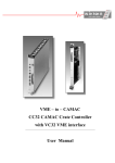
W-ie-
W erk für
e-R
Plein & Baus GmbH
I ndustriee lektronik
N ukleare lektronik
Regelungstechnik
PCI-CAMAC
CC32 CAMAC Crate Controller
with PCI Interface
User Manual
General Remarks
The only purpose of this manual is a description of the product. It must not be interpreted a
declaration of conformity for this product including the product and software.
W-Ie-Ne-R revises this product and manual without notice. Differences of the description in
manual and product are possible.
W-Ie-Ne-R excludes completely any liability for loss of profits, loss of business, loss of use or
data, interrupt of business, or for indirect, special incidental, or consequential damages of any kind,
even if W-Ie-Ne-R has been advises of the possibility of such damages arising from any defect or
error in this manual or product.
Any use of the product which may influence health of human beings requires the express written
permission of W-Ie-Ne-R.
Products mentioned in this manual are mentioned for identification purposes only. Product names
appearing in this manual may or may not be registered trademarks or copyrights of their respective
companies.
No part of this product, including the product and the software may be reproduced, transmitted,
transcribed, stored in a retrieval system, or translated into any language in any form by any means
with the express written permission of W-Ie-Ne-R.
CC32, VMEMM, PCIADA and VC32 (VMEADA) are designed by ARW Elektronik, Germany.
November 00
ii
*00479.A1
Table of contents:
Legend:
1
PCI-CAMAC SYSTEM: GENERAL DESCRIPTION ....................................................................................... 1
1.1
SUMMARY PCIADA / CPCIADA ..................................................................................................................... 1
1.2
SUMMARY CC32 CAMAC CRATE CONTROLLER .............................................................................................. 1
1.3
FRONT PANEL .................................................................................................................................................... 2
1.4
INSTALLATION PCIADA AND CC32 ................................................................................................................. 3
1.4.1 ATTENTION............................................................................................................................................... 3
1.4.2 Installation ................................................................................................................................................... 3
1.5
CRATE NUMBER................................................................................................................................................. 4
1.6
ACCESS TIMES AND PERFORMANCE ................................................................................................................... 4
2
PCIADA INTERFACE CARD .............................................................................................................................. 5
2.1
32 KBYTES ADDRESS RANGE............................................................................................................................. 5
2.2
GENERAL DESCRIPTION AND FUNCTION ..................................................................................................... 5
2.3
MAJOR PC-REGISTER (PCR) ............................................................................................................................. 5
2.4
MAJOR LC-REGISTERS (LCR)........................................................................................................................... 6
2.4.1 Interrupt Control/Status Register ................................................................................................................. 6
2.4.2 User I/O Register / Reset Interrupt .............................................................................................................. 7
2.5
ACCESS-TIMEOUT ............................................................................................................................................. 7
2.6
INTERRUPTS....................................................................................................................................................... 7
2.7
POWER CONSUMPTION ...................................................................................................................................... 8
2.8
PCIADA LAYOUT ............................................................................................................................................. 8
3
CC32 CONTROLLER ........................................................................................................................................... 9
3.1
SPECIAL FEATURES ........................................................................................................................................... 9
3.1.1 FASTCAMAC basic Level 1....................................................................................................................... 9
3.1.2 CAMAC-Cycle-Tuning ............................................................................................................................... 9
3.1.3 DATAWAY-DISPLAY............................................................................................................................... 9
3.2
CC32 NORMAL-STATION ................................................................................................................................ 10
3.3
NAF COMMANDS AND ADDRESSING ............................................................................................................... 10
3.3.1 NAF bit coding .......................................................................................................................................... 10
3.3.2 NAF calculation......................................................................................................................................... 10
3.4
CC32 ADDRESS MAP ....................................................................................................................................... 11
3.5
CC32-STATUS .............................................................................................................................................. 12
3.6
CC32-C,Z,INHIBIT,LAM-FF ...................................................................................................................... 13
3.7
BROADCAST-MASK-REGISTER .................................................................................................................. 13
3.8
BROADCAST CAMAC-WRITE ................................................................................................................... 13
3.9
LAM-MASK-REGISTER ............................................................................................................................... 13
3.10 LAM-AND-STATUS........................................................................................................................................ 14
3.11 LAM-NOT-STATUS ........................................................................................................................................ 14
3.12 LAM-BUS-STATUS ....................................................................................................................................... 14
3.13 LED-STATUS ................................................................................................................................................ 14
3.14 CAMAC CYCLE-TUNE-REGISTER .................................................................................................................. 15
3.15 CC32-RESET ................................................................................................................................................... 15
3.16 POWER CONSUMPTION ..................................................................................................................................... 15
3.17 COMPONENT LOCATION CC32 CONTROL-STATION ......................................................................................... 17
3.18 COMPONENT LOCATION CC32 NORMAL-STATION .......................................................................................... 18
3.19 CC32 DATA WAY CONNECTOR PIN ASSIGNMENT ............................................................................................. 19
November 00
iii
*00479.A1
User’s Manual
PCI-CAMAC
W-Ie–Ne-R
Plein & Baus GmbH
1 PCI-CAMAC SYSTEM: General description
With the help of the PCI-CAMAC system which consists of CAMAC crate controller CC32 and
the PCI card PCIADA, users of the CAMAC bus profit of the technical success, which takes place
in the PC development. For a fast and efficient CAMAC control and data read-out the system
supports 16-bit and 32-bit wide data transfers.
A huge variety of software is available for a PC. In parallel it’s performance was constantly
improved. Modern operating systems were developed which turn the PC into a powerful
workstation. On the other hand the number of UNIX workstations which are equipped with PCI
increases strongly. The PCI-CAMAC system can be used in this environment too.
Drivers and programming tools for PCI-CAMAC are provided for different operating systems and
programming languages.
Drivers for Windows-95/98 and Windows-NT offers an easy access to CAMAC data way. For C
and Turbo Pascal users the Pascal and C-libraries provide easy routines to operate CAMAC
modules.
Working with the LINUX driver all advantages of UNIX multi user and multi tasking operating
system can be used for CAMAC operations.
The PCIADA interface card supports 16 and 32 – bit PCI bus slave access. It provides
programmable interrupt generation on PC. PCIADA is also compatible to the PCI-VME system.
To link CAMAC systems equipped with the CC32 into a VME based data acquisition a VME slave
module VC32(VMEADA) is available, which can replace the PCIADA in this case.
1.1
Summary PCIADA / CPCIADA
•
•
•
•
•
•
1.2
PCI-interface based on standard PCI chip PLX9050 produced by PLX-Technology
support of (8), 16 u. 32 bit PCI-bus slave accesses
direct data mapping into the target address area with automatic „low-big-endian“ conversion.
use of 32K memory segment below the 1MB limit to be accessible for MS-DOS applications
supports interrupt source from CC32 (maskable LAM) and local „timeout“ interrupt source
differential bus driver and receiver for fast and reliable data transfer
Summary CC32 CAMAC crate controller
•
transparent D16 and D24 (D32) CAMAC data way access
32K NAF coding / addressing
•
24 bit programmable LAM-mask register
•
LAM-interrupt transfer to PCIADA
•
FASTCAMAC Level 1
LED-display for:
+6V
CAMAC-access, local CC32-access, INHIBIT and LAM. (stretched to 5 ms)
CAMAC data way display for: Q, X, C, Z, N1...16, A1…8, F1…16 and Data1…24.
CAMAC-cycle tuning (Busy to S1) for each station, range 300ns and 200ns, S1/S2=100ns
Broadcast CAMAC-WRITE and broadcast-mask register
no interference of PC operation due to CAMAC crate on / off changes (if interrupt disabled)
•
•
•
•
•
November 00
1
*00479.A1
User’s Manual
W-Ie–Ne-R
PCI-CAMAC
Plein & Baus GmbH
1.3
Front Panel
CC32
CAMAC-CONTROLLER
Power
Local Acces
Camac Acces
Inhibit
LAM Flip-Flop
Q-Acknowledge
X-Acknowledge
Clear-Cycle
Initialise-Cycle
stredched to
5 ms
Station Number
Sub-Addres
Funktion
Connector
to
PCIADA or VC32(VMEADA)
Camac-Data
November 00
2
*00479.A1
User’s Manual
PCI-CAMAC
W-Ie–Ne-R
Plein & Baus GmbH
1.4
1.4.1
Installation PCIADA and CC32
ATTENTION
Observe precautions for handling:
• Electrostatic device! Handle only at static safe work stations. Do not touch electronic components
or wiring
• The CAMAC crate as well as the used PC have to be on the same electric potential. Different
potentials can result in unexpected currents between the CC32 and PCIADA which can destroy
the units.
• Do not plug the CC32 into a CAMAC crate under power. Switch off the CAMAC crate first
before inserting or removing any CAMAC module! For safety reasons the crate should be
disconnected from AC mains.
• Do not plug in the PCIADA into a PC under power. First switch off the computer and disconnect
from AC mains.
1.4.2
Installation
1. Check the CC32 jumpers and set them according to the required functionality (see 1.5. Crate
number ). There are no user-definable settings on the PCIADA-card.
2. Turn off the PC and any peripheral equipment. Remove the power cable .
3. Remove the computer outside cover and locate a free PCI-expansion slot.
4. Carefully slide the PCIADA card into the PCI slot. After the card is firmly in secure it’s fastening
tab to the PC chassis with a screw.
5. Replace the PC cover and power cord.
6. Switch off the CAMAC crate and remove the power cord. Plug in the CC32 on the far right slots
(normally slot 24 & 25) and secure it with the front panel screw.
7. Attach one end of the 50-pin cable to the CC32 connector and the other side to the PCIADA card.
8. Switch on the CAMAC crate and the PC. The Plug-and-Play Bios should automatically recognize
the card.
9. Install the PCIADA/CC32 driver from the attached CD-ROM as described within the driver
manual for your operating system.
10. To work with DOS based programs accessing the PCI-CAMAC system add or modify the
EMM386.EXE line in the CONGIG.SYS (as shown on the CD-ROM at
\DOS\PASCAL\Readme.txt).
11. Test the installation with the software delivered on CD-ROM.
November 00
3
*00479.A1
User’s Manual
W-Ie–Ne-R
PCI-CAMAC
Plein & Baus GmbH
1.5
Crate number
Using more than one PCIADA cards in one PC to control multiple CAMAC crates requires to differ
between the connected CC32 controllers. For this purpose a crate number can be defined by jumper
setting on the CC32 board. Please see the location of the jumper array on the component scheme (see
3.17).
Attention: If using multiple CC32 controllers with the same crate number connected to PCIADA
cards in one PC it is not possible to differ between the CAMAC controllers and to access them. This can
result in unexpected effects.
The actual crate number setting can be determined by software reading the CC32-Status.
J304 J303 J302 J301 Function
Crate number for multiple PCI-CC32 installations
x
x
x
x
(factory prepared setting, crate number = 1)
I
I
I
:
=
jumper is installed
I
=
jumper is not installed
:
1.6
Access times and performance
Typical access times based on a Pentium 133MHz (including reading of program-code):
Access type
WR-time / us
PCI to CC32 internal D16
PCI to CC32 internal D32
PCI to CC32 Dataway D16
PCI to CC32 Dataway D32 (R/W24)
PCI to CC32 Dataway FAST LEVEL1 D32 (D24)
0,6
0,65
1,4 (1,2)
1,4 (1,2)
-
RD-time / us
1,0
1,5
1,8 (1,6)
2,0 (1,8)
1,5
Values in brackets ( ..) are obtained with Cycle-Tune bits = 11
November 00
4
*00479.A1
User’s Manual
W-Ie–Ne-R
PCI-CAMAC
Plein & Baus GmbH
2
PCIADA INTERFACE CARD
2.1
32 Kbytes Address range
Attention: The CAMAC version of PCIADA to be used with the CAMAC controller CC32
is configured to use a 32 Kbytes address area instead of the original 8K for use with VMEMM.
Thus instead of address bits A0 and A1 the higher address bits A13 u. A14 are transmitted. The
CAMAC version of PCIADA is labeled with a “C” on the EEPROM.
If necessary it is possible to re-program the EEPROM. This can be done by the user via the computer
where the PCIADA is plugged in.
All instructions are given on the enclosed CD-ROM at WORKAROUND.TXT
2.2
General description and function
Attention: It is assumed that the PC is equipped with a self-configuring PCI-BIOS (“Plugand-Play Bios “) which automatically recognizes the card.
To guarantee a maximum PCI compatibility and performance the PCIADA is based on the
PCI-bus target- interface-Chip PLX9050 produced by PLX-Technology, which manages the PCI
communication.
At booting time necessary settings are configured by PCI auto setup. No jumpers have to be
set on the interface card. All PCIADA information such as memory and IRQ requirements are
stored in an EEPROM. Some IDs can be read out from PCR:
During PCI setup PCIADA calls for three different memory areas:
1. 54 byte Local Configuration Register (LCR) of the I/O area. Different control status
register and base addresses are available in the LCR. Note: Some computer architectures
do not provide register mappings in the I/O area. Please refer to LCR in memory area.
2. 32 Kbytes of the memory area for direct access to local CC32 address space and
transparent CAMAC data way access
2.3 Major PC-Register (PCR)
The following ID’s are used to identify the connected hardware. These values are determined by
the PCI-Bios and software drivers:
ID
Vendor ID
Device ID
Subsystem Vendor ID
Subsystem Device ID
November 00
PCIADA Defined value
for CC32
0x10B5
0x2258
0x9050
0x2258
5
PCIADA Defined value
for VMEMM (ref. only)
0x10B5
0x9050
0x9050
0x1167
*00479.A1
User’s Manual
PCI-CAMAC
W-Ie–Ne-R
Plein & Baus GmbH
2.4
Major LC-Registers (LCR)
According to the PCI specification the Base addresses for the LC-Register and CC32
memory areas are automatically allocated during booting of the computer. They can be obtained
via BIOS from the PLX chip. Please refer to the software section and the PCI9050 data sheet on
the CD-ROM. ( see CD-ROM ..PCIADA\Chipdocu\9050-1ds.pdf)
There are no additional registers to be programmed by the user.
2.4.1
Interrupt Control/Status Register
INTERRUPT-1
Interrupt requests, initiated by CC32 (LAM-FF), will set INTERRUPT-1 status bit to 1. For this
purpose the interrupt request has to be enabled.
INTERRUPT-2
The INTERRUPT-2 status bit will be activated by local PCIADA events. The following sources can
cause INTERRUPT-2:
1. Access without connection between CC32 and PCIADA (no cable connection)
2. Access to CAMAC crate which is not switched on (CC32 not working)
3. CC32 access has not yet been enabled. The user bit I/O 2 has to be set to enable the access to the
CAMAC crate controller.
INTCSR; LCR-Baseadr + 0x4c ( by word-access)
byte
0
1
2
3
4
5
6
7
15..8
RD WR after Init
Local Interrupt 1 enable: 1 = enable / 0 = disable (source = CC32)
Local Interrupt 1 polarity : 1 = active high / 0 = active low
Local Interrupt 1 status: 1 = active. 0 = not active
Local Interrupt 2 enable: 1 = enable / 0 = disable (source = PCIADA)
Local Interrupt 2 polarity: 1 = active high / 0 = active low
Local Interrupt 2 status: 1 = active. 0 = not active
PCI Interrupt enable: 1 = enable / 0 = disable (source = global)
Software Interrupt: 1 = generate Interrupt
not used
November 00
6
yes
yes
yes
yes
yes
yes
yes
yes
yes
yes
yes
no
yes
yes
no
yes
yes
no
1
0
0
1
0
0
0
0
00000000 b
*00479.A1
User’s Manual
PCI-CAMAC
W-Ie–Ne-R
Plein & Baus GmbH
2.4.2
User I/O Register / Reset Interrupt
USERI/O2:
The User I/O Register (CNTRL) is divided into two parts which are summarized in the
following. The register USER I/O2:
1. locks CC32 during boot time to prevent any access of the Operating System.
2. resets interrupt 2 if it is deleted.
USER I/O3:
Register USER I/O3 monitors the status of the CAMAC crate and the cable connection, i.e. it shows the
switched on CAMAC crate and the proper cable connection.
CNTRL; LCR-Baseadr + 0x50 ( by word-access)
byte
5..0
6
7
8
9
10
11
15..12
RD WR after Init
do not modify !
USER I/O2 Type, must always be 0
USER I/O2 Direction, must always be 1 = output
USER I/O2 output, 0 = disable access to CC32, 1 = enable access
USER I/O3 Type, must always be 0
USER I/O3 Direction, must always be 0 = input
USER I/O3 Input, 0 = CC32 failed , 1 = CC32 OK
do not modify
yes
yes
yes
yes
yes
yes
yes
yes
yes
yes
yes
yes
yes
yes
no
yes
000100 b
0
1
0
0
0
0
0100 b
Write 0x4184 for enable access to CC32
Write 0x4084 for disable access to CC32
2.5
Access-Timeout
An Access Timeout is implemented in the PCIADA interface, which is currently set to about 35 µs.
Reaching this time-out the current transaction will be terminated and an INTERRUPT-2 initiated. If the
CC32 is switched off or disconnected the same INTERRUPT-2 is activated.
2.6
Interrupts
The PCI-CAMAC system can generate interrupts on the PC caused by two different interrupt sources.
PCIADA can activate a Timeout Interrupt which should be routed via software to the interrupt vector
number 1. All CC32 generated interrupts should be routed via software to the interrupt vector number 2.
Interrupt Source
Vector No.
PCIADA Interrupt (Timeout)
1
CC32 Interrupt (LAM-FF)
2
November 00
7
*00479.A1
User’s Manual
W-Ie–Ne-R
PCI-CAMAC
Plein & Baus GmbH
2.7
Power Consumption
Voltage
+5V
2.8
Max. current
ca. 0,5 A
Power
Ca. 2,5W
PCIADA Layout
November 00
8
*00479.A1
User’s Manual
PCI-CAMAC
W-Ie–Ne-R
Plein & Baus GmbH
3
3.1
CC32 CONTROLLER
Special Features
3.1.1 FASTCAMAC basic Level 1
The CC32 CAMAC crate controller supports the FAST CAMAC (see DOE/SC-0002 or
http://www.yale.edu/fastCAMAC) BASIC level 1 using multiple S1 strobes to increase the data transfer
speed (theoretical max. 7.5Mbytes/s). As defined within the FAST CAMAC specification the function
code F = 5 is used to read data from a module supporting this mode. Getting the first data set in this
mode the controller continues automatically to read the following one to have it available without any
delay for the next data request from the computer. Thus it is possible to read data with the maximum
transfer rate between CC32 and PCIADA which saves about 400ns per read-cycle. This FAST CAMAC
level 1 read via F = 5 is stopped if the Q-response is missing.
The FAST CAMAC level 1 cycle can be interrupted by another F –command. In this case the new
command is executed correctly however, the data which have been already buffered in the CC32 are lost.
3.1.2
CAMAC-Cycle-Tuning
For optimized timing it is possible to adjust the CAMAC cycle time (time between begin of BUSY =
active to S1) for each individual CAMAC station C-Station via software. Possible values are 200ns,
300ns and 400ns (default). In addition the width of the S1 and S2 strobe signals can be set optionally to
100ns.
3.1.3
DATAWAY-DISPLAY
To extend the functionality of the CC32 crate controller it is equipped with an integrated CAMAC
data way display. This allows to monitor the activity in the CAMAC crate and is a helpful tool to locate
faults in the system. The internal data registers (data and control bits) used for this purpose can be
accessed also in CC32 controllers without display. The CC32-LED card which is internally plugged onto
the CC32 normal station shows the following signals with color LED’s:
•
Station number N1, N2, N4, N8 and N16
•
Sub-address A1, A2, A4 and A8
•
Function F1, F2, F4, F8 and F16
•
Data 1 – 24 (shared for R1...R24 and W1...W24
•
Q, X, (Q and X response)
•
C, Z (Clear) and Z (Initialize)
•
I (Inhibit)
•
Local and CAMAC cycle
•
LAM (Look-at-me request from station)
• 6V power line
Please note that the N LED is also responding on local CC32 commands.
November 00
9
*00479.A1
User’s Manual
PCI-CAMAC
W-Ie–Ne-R
Plein & Baus GmbH
3.2
CC32 Normal-Station
To allow an easy test of the controller and PCIADA to CC32 connection the following test functions
are implemented in the CC32 Normal-Station. The station number Nn corresponds to the left one of the
two CAMAC slots occupied by the CAMAC controller. As given in 1.4.2 the CC32 has to be plugged in
into the most right slots of the CAMAC crate (normally slot 24 and 25).
( Nn = CC32 Control-Station – 1 )
Write
Nn * A0 * F16 data <> 5
Nn * A0 * F16 data = 5
Nn * A1 * F16 data = 0..15
generate Q and X
generate Q ,X and LAM ( LAM 200ns active)
load test counter, generate Q and X
Read
Nn * A0 * F0 data = 0
generate Q and X
Read in Fast CAMAC Level 1 mode
Nn * A1 * F5 data = 0
3.3
decrement test counter, generate X and Q only if
test counter content > 0
NAF Commands and Addressing
A 32 Kbytes memory window is used to access the CC32 and to perform CAMAC operations. This 32
Kbytes area is mapped into the PCI address space. The position (e.g. Basic address) within the PCI
address space is dynamically allocated.
For CAMAC commands the N, A and F numbers are coded into the Address bits A14 … A2. Thus
these bits have to be understood as NAF bits. Also local calls are performed as NAF commands. Only
word and long word accesses are possible to the CC32 (see 3.4.)
3.3.1
NAF bit coding
32K address CC32
CAMAC-Function-bit
3.3.2
A14 A13 A12 A11 A10 A9 A8 A7 A6 A5 A4 A3 A2 A1 A0
N16 N8 N4 N2 N1 A4 A3 A2 A0 F8 F4 F2 F1 -
NAF calculation
The F16 bit is automatically defined by the kind of operation, i.e. it is not considered in the NAF code
calculation!
WRITE to CC32 defines automatically F16 = 1.
READ from CC32 defines automatically F16 = 0.
The different address offsets for N, A and F into the 32 Kbytes memory window can be
calculated as shown below:
Pascal: NAF := N shl 10 + A shl 6 + (F AND $f) shl 2;
C / C++: #define MAKE_CC32_OFFSET(N,A,F) ((N<<10) + (A<<6) + ((F & 0xf)<<2))
November 00
10
*00479.A1
User’s Manual
PCI-CAMAC
W-Ie–Ne-R
Plein & Baus GmbH
To reduce the time required by the software for coding the NAF address it can be helpful to
define constants for these values in the user program. This can increase the data rates. Further it
is recommended to set the F16-bit to 0 before calculating the address as shown above to avoid
an overlap with the A1 bit.
3.4
CC32 Address map
The 32 Kbytes memory window can be accessed only by word and long word calls. byte calls are not
processed and answered by the CC32. They are terminated by a TIME-OUT signal from the PCIADA
card. All word and long word calls are accepted by the CC32. Please note in case of a long word (Lword)
access to an address specified for word only :
Long word-Read from CC32 word address: D31..D16 equals to D15..D00.
Long word-Write to CC32 word address: only D15..D00 will be transferred. D31..D16 are ignored.
All CC32-commands described following are given within the CAMAC NAF-notation. This includes
internal CC32 commands. The gray marked cells in the next table indicate operations to the CAMAC
stations via the CAMAC data way. All the other described commands are special functions of the CC32
controller.
NAF
N31*A0*Fx
N30*A2*Fx
Access
Word
Word
N30*A1*Fx
Word
N30*A0*Fx
N29*A0*Fx
Word
Lword
N28*A4*Fx
Lword
N28*A3*Fx
Lword
N28*A2*Fx
Lword
N28*A1*Fx
Lword
N28*A0*Fx
Word
November 00
WR-Function / F16-bit=1
CC32 RESET
CYCLE-TUNE-RegC
D15..D00 >> N24..N17
CYCLE-TUNE-RegB
D15..D00 >> N16-N9
CYCLE-TUNE-RegA
D15..D00 >> N8..N1
-
RD-Function / F16-bit=0
CYCLE-TUNE-RegC
D15..D00 << N24..N17
CYCLE-TUNE-RegB
D15..D00 << N16..N9
CYCLE-TUNE-RegA
D15..D00 << N8..N1
LED-Status
D23..D00 << LED24..LED1
D27..D24 << C,Z,CT1,CT0
D31..D28 << Q,X,INH,LAM-FF
LAM-BUS
D23..D00 << LAM24..LAM1
D31..D24 is equal LAM-MASK
LAM-NOT = LAMn & !LMASKn
D23..D00 << NOT24..NOT1
D31..D24 is equal LAM-MASK
LAM-AND = LAMn & LMASKn
D23..D00 << AND24..AND1
D31..D24 is equal LAM-MASK
LAM-MASK
LAM-MASK
D23..D00 >> LMASK23-LMASK0 D23..D00 << LMASK24..LMASK1
D31..D24 = xx
D27..D24 = 0
D28 = LAM-BUS-OR
D29 = LAM-NOT-OR
D30 = LAM-AND-OR
D31 = LAM-FF
LAM_FF reset
LAM-FF Status
D15..D00 = xx
D00 = 1 LAM-FF set
D00 = 0 LAM-FF not set
D15..D01 = 0
11
*00479.A1
User’s Manual
W-Ie–Ne-R
PCI-CAMAC
Plein & Baus GmbH
N27*A0*Fx
N27*A1*Fx
Word
N26*A0*Fx
Lword
N25*Ax*Fx
Lword
N1-24*Ax*Fx
Lword
N1-24*Ax*Fx
Word
N0*A0*Fx
N0*A1*Fx
N0*A2*Fx
N0*A3*Fx
Word
*1
*2
*3
*4
3.5
INHIBIT on
INHIBIT off
D31..D00 = xx
INHIBIT Status
D00 = INHIBIT on = 1
D01 = INHIBIT Dataway on = 0
D15..D02 = 0
Broadcast-MASK
Broadcast-MASK
D23..D00 >> BMASK24..BMASK1 D23..D00 << BMASK24..BMASK1
D24..D31 << 0
Broadcast-WR=allN & BMASKn D23..D00 >>W1..W24
CAMAC-DATAWAY WRITE *1 CAMAC-DATAWAY READ
*1
D23..D00 >> W24..W1
*3 D23..D00 << R23..R00
D29..D24 = 0
D31,D30 Q,X
CAMAC-DATAWAY WRITE *1 CAMAC-DATAWAY READ
*1
D00..D15 > W1..W16
*3 D00..D15 < R1..R16
*4
CAMAC C
*2 CC32-STATUS
CAMAC Z
*2 D03..D00 << Q,X,INH,LAM-FF
CAMAC C + INHIBIT off
*2 D07..D04 << Modul-Number
CAMAC Z + INHIBIT on
*2 D11..D08 << FPGA-Revision
D15..D12 << Modul-Type 1000b
D15..D00 = xx
Standard CAMAC -Access
Standard CAMAC -Access without S1
no W-Data on CAMAC -Dataway when F8-bit is active
if test Q- or X-Status then use Lword-Access
CC32-Status
(Read Word)
N0*A0*Fx
This register contains the CC32 configuration and status, including the CAMAC status lines Q, X, I
and LAM. The module type identification (bit 12 .. 15) and module number (bit 4 … 7) can be used to
identify the CC32.
CC32-Status (word read access only)
Bit
15..12
RD WR after Init
Module type identification, 1000b for CC32 (0001b VMEMM)
yes
no
1000b
11..8
FPGA-Revision
yes
no
xxxx
7..4
Module number, Coding of Jumpers J304..J301
yes
no
Jumpers
3
Q – Response
yes
no
x
2
X – Response
yes
no
x
1
State of Inhibit-Flip-Flop
yes
no
0
0
State of LAM-Flip-Flop
yes
no
0
November 00
12
*00479.A1
User’s Manual
W-Ie–Ne-R
PCI-CAMAC
Plein & Baus GmbH
3.6
CC32-C,Z,Inhibit,LAM-FF
N0*A0*Fx
N0*A1*Fx
N0*A2*Fx
N0*A3*Fx
N27*A0*Fx
N27*A1*Fx
N28*A0*Fx
3.7
=
=
=
=
=
=
=
C (CAMAC Clear)
Z (CAMAC Initialize)
C + Inhibit off
Z + Inhibit on
Inhibit on
Inhibit off
LAM-FF reset
(Write Word)
(Write Word)
(Write Word)
(Write Word)
(Write Word)
(Write Word)
(Write Word)
Broadcast-Mask-Register
(Read/Write Lword)
N26*A0*Fx
Allows to enable / disable CAMAC stations for broadcast write commands. All stations (N1 … N24)
with Broadcast mask bit = 1 are enabled.
Data
Broadcast-Mask for:
3.8
D23 D22 D21..D3
N24 N23 N22..N4
D2
N3
D1
N2
D0
N1
Broadcast CAMAC-Write
(CAMAC-Write-Cycle Word or Lword)
N25*Ax*Fx
Broadcast write command, has to be performed with a correct A(x), F(x) and W-Data CAMAC
command. Stations N1..N24 are active for this write operation if the corresponding Broadcast-Maskbit is 1.
3.9
LAM-Mask-Register
(Read/Write Lword)
N28*A1*Fx
All stations (with station number N) with enabled Broadcast Mask-bit (=1) can generate a LAM-FF in
the CC32 controller which can yield in an interrupt on the PCIADA card.
Data
Enable LAM from Station
D23
N24
D22
N23
D21..D3
N22..N4
D2
N3
D1
N2
D0
N1
The negative edge of the LAM-signal arriving from any station is only transmitted to the LAM-FlipFlop if the corresponding LAM-Mask-bit is active (=1). The LAM-FF stays on the active level until a
reset command N28*A0*F16 occurs.
The following status bits can be used to get a more detailed information about the LAM conditions:
D28 = 1 (LAM-BUS-OR) if at least one LAM is pending
D29 = 1 (LAM-NOT-OR) if at least one LAM is pending from disabled stations (LAM-Maskbit =0)
D30 = 1 (LAM-AND-OR) if at least one LAM is pending from enabled stations (LAM-Maskbit =1)
D31 = 1 (LAM-Flip-Flop) if LAM request
November 00
13
*00479.A1
User’s Manual
W-Ie–Ne-R
PCI-CAMAC
Plein & Baus GmbH
3.10 LAM-AND-Status
(Read Lword)
N28*A2*Fx
Dxx = 1 if LAM = active and LAM-Maskbit = 1.
Data
LAM status & LMASK
D23
N24
D22
N23
D21..D3
N22..N4
D2
N3
D1
N2
D0
N1
D21..D3
N22..N4
D2
N3
D1
N2
D0
N1
D2
N3
D1
N2
D0
N1
( bits D28..D31 as described in 3.8)
3.11 LAM-NOT-Status
(Read Lword)
N28*A3*Fx
Dxx = 1 if LAM = active and LAM-Maskbit = 0.
Data
D23
LAM Status & not LMASK N24
D22
N23
( bits D28..D31 as described in 3.8)
3.12 LAM-BUS-Status
(Read Lword)
N28*A4*Fx
Dxx = 1 if LAM = active.
LAM-BUS
LAM Status CAMAC-Bus
D23 D22
N24 N23
D21..D3
N22..N4
( bits D28..D31 as described in 3.8)
3.13 LED-Status
(Read Lword)
N29*A0*Fx
This function can be used to read back the information of the optional dataway display. If no dataway
display is installed the function can be used to determine the CAMAC data and status signals of the last
CAMAC dataway operation. The LED24..LED1 bits correspond to the write (W) or read (R) data of the
last CAMAC cycle.
Data D24..D29 used for CC32 functional tests.
Data
LED-Status
D23 D22 D21..D3
LED LED LED22..LED3
24
23
D2 D1 D0
LED LED LED
3
2
1
Data
LED-Status
D31
Q
D26
CT0
November 00
D30 D29
D28
D27
X Inhibit LAM-FF CT1
14
D25
Z
D24
C
*00479.A1
User’s Manual
W-Ie–Ne-R
PCI-CAMAC
Plein & Baus GmbH
3.14 CAMAC Cycle-Tune-Register
(Write/Read Word)
N30*A2*Fx Register-C for station N24..N17
(Write/Read Word)
N30*A1*Fx Register-B for station N16..N9
(Write/Read Word)
N30*A0*Fx Register-A for station N8..N1
For optimized timing it is possible to adjust the CAMAC cycle time (time between begin of BUSY =
active to negative edge of S1 strobe signal) for each individual CAMAC station. Possible values are
200ns, 300ns and 400ns (default). In addition the width of the S1 and S2 strobe signals can be set
optionally to the shorter value of 100ns.
For each station this is done by defining the 2-bit CT1 and CT0 registers. These registers are in the
following named Nx-1 and Nx-0 to consider the station number.
Nx-1,Nx-0 = 00 > 400ns CAMAC-Standard
Nx-1,Nx-0 = 01 > 300ns
Nx-1,Nx-0 = 10 > 200ns
Nx-1,Nx-0 = 11 > 200ns / S1 and S2 = 100ns
Register map:
DATA
Cycle-tune RegC
Cycle-tune RegB
Cycle-tune RegA
D07
N20-1
N12-1
N4-1
D06
N20-0
N12-0
N4-0
D05
N19-1
N19-1
N3-1
D04
N18-0
N11-0
N3-0
D04
N18-1
N18-1
N2-1
D02
N18-0
N10-0
N2-0
D01
N17-1
N9-1
N1-1
D00
N16-0
N9-0
N1-0
DATA
Cycle-tune RegC
Cycle-tune RegB
Cycle-tune RegA
D15
N24-1
N17-1
N8-1
D14
N24-0
N16-0
N8-0
D13
N23-1
N^5-1
N7-1
D12
N23-0
N15-0
N7-0
D11
N22-1
N14-1
N6-1
D10
N22-0
N14-0
N6-0
D09
N21-1
N13-1
N5-1
D08
N21-0
N13-0
N5-0
Attention: These options do not confirm the CAMAC standard. They can be used to improve
the data transfer and / or the communication with CAMAC modules. It has to be tested by the
user which CAMAC module can be used for different CAMAC cycle timing.
3.15 CC32-Reset
N31*A0*Fx
(Write Word)
Resetting the CC32 initializes the following registers:
•
Inhibit-FF
•
LAM-FF
•
BROADCAST-MASK-, and LAM-MASK-REGISTER
•
CYCLE-TUNE-REGISTER
3.16 Power consumption
Voltage
November 00
Current
Power
15
*00479.A1
User’s Manual
W-Ie–Ne-R
PCI-CAMAC
Plein & Baus GmbH
+6V
November 00
1,7 A
10,2 W
16
*00479.A1
User’s Manual
W-Ie–Ne-R
PCI-CAMAC
Plein & Baus GmbH
U102
U104
U106
U108
U202
U204
U203
green
yellow
green
yellow
red
3.17 Component location CC32 Control-Station
U301
U501
U401
U402
17
U506
U507
U508
U503
U504
U505
U303
U302
U502
November 00
*00479.A1
November 00
18
U103
U102
U204
U205
U206
U107
U104
U106
U101
U201
U202
U203
U105
yellow
yellow
yellow
yellow
green
green
green
green
yellow
yellow
yellow
yellow
green
green
green
green
yellow
yellow
yellow
yellow
green
green
green
green
yellow
green
green
green
green
green
green
green
green
yellow
green
green
green
green
yellow
green
yellow
green
User’s Manual
PCI-CAMAC
W-Ie–Ne-R
Plein & Baus GmbH
3.18 Component location CC32 Normal-Station
*00479.A1
User’s Manual
W-Ie–Ne-R
PCI-CAMAC
Plein & Baus GmbH
3.19 CC32 data way connector pin assignment
CC32 pin assignment
Normal-Station
Sig.Top
X
I
C
N
L
S1
S2
W24
W22
W20
W18
W16
W14
W12
W10
W8
W6
W4
W2
R24
R22
R20
R18
R16
R14
R12
R10
R8
R6
R4
R2
Gnd
November 00
Nr.
1
2
3
4
5
6
7
8
9
10
11
12
13
14
15
16
17
18
19
20
21
22
23
24
25
26
27
28
29
30
31
32
33
34
35
36
37
38
39
40
41
42
43
Contol-Station
Sig.Bott.
B
F16
F8
F4
F2
F1
A8
A4
A2
A1
Z
Q
W23
W21
W19
W17
W15
W13
W11
W9
W7
W5
W3
W1
R23
R21
R19
R17
R15
R13
R11
R9
R7
R5
R3
R1
Sig.Top
X
I
C
S1
S2
L24
L23
L22
L21
L20
L19
L18
L17
L16
L15
L14
L13
L12
L11
L10
L9
L8
L7
L6
L5
L4
L3
L2
L1
+6
Gnd
Gnd
19
Nr.
1
2
3
4
5
6
7
8
9
10
11
12
13
14
15
16
17
18
19
20
21
22
23
24
25
26
27
28
29
30
31
32
33
34
35
36
37
38
39
40
41
42
43
Sig.Bott.
B
F16
F8
F4
F2
F1
A8
A4
A2
A1
Z
Q
N24
N23
N22
N21
N20
N19
N18
N17
N16
N15
N14
N13
N12
N11
N10
N9
N8
N7
N6
N5
N4
N3
N2
N1
+6
Gnd
*00479.A1