1
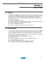
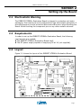
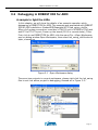
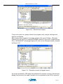
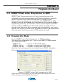
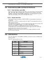
EMBEST ATEB40x User Guide
Face
ATEB40x Evaluation Board
......................................................................................
User Guide
Shenzhen Embest Info &Tech Co., LTD.
Tel: +86-755-25635626/25635656
E-mail: [email protected]
All rights reserved.
Fax: +86-755-25616057
[email protected]
Room 509, Luohu Science &Technology Building, #85 Taining Road,
Shenzhen, Guangdong, China. http://www.embedinfo.com
Page 1
EMBEST ATEB40x User Guide
Table of Content
Section 1 Overview ....................................................................................................................3
1.1
Scope................................................................................................................................................ 3
1.2
Deliverables ..................................................................................................................................... 3
1.3
The EMBEST ATEB40x Evaluation Boar....................................................................................... 4
Section 2 Set up the Board .........................................................................................................5
2.1
Electrostatic Warning....................................................................................................................... 5
2.2
Requirements ................................................................................................................................... 5
2.3
Layout .............................................................................................................................................. 5
2.4
Jumper Settings................................................................................................................................ 6
2.5
Powering Up the Board.................................................................................................................... 7
Section 3 Debugging in Embest IDE for ARM .........................................................................8
3.1
EMBEST ATEB40x test programs .................................................................................................. 8
3.2
Debugging in EMBEST IDE for ARM.......................................................................................... 10
Section 4 Program into Flash ...................................................................................................14
4.1
EMBEST Flash online Programmer for ARM............................................................................... 14
4.2
Program into Flash......................................................................................................................... 14
Section 5 Circuit Discription....................................................................................................15
5.1
Support Processors......................................................................................................................... 15
5.2
Expansion Connectors ................................................................................................................... 15
5.3
Memories ....................................................................................................................................... 15
5.4
Power and Crystal Quartz .............................................................................................................. 15
5.5
Push-buttons,LEDs and Serial Interfaces ...................................................................................... 16
5.6
LCD Interface ................................................................................................................................ 16
5.7
Reset Circuit and JTAG Interface .................................................................................................. 17
Customer Service .....................................................................................................................18
Copywrite©2003 by Shenzhen EMBEST Info&Tech Co.,LTD.
All rights reserved.
No part of this document may be reproducted or transmitted in any form or by any means without
prior written consent of EMBEST Info&Tech Co.,LTD.
EMBEST® is registered trademarks of EMBEST Info&Tech Co.,LTD.
Page 2
EMBEST ATEB40x User Guide
Section 1
Overview
1.1
Scope
The EMBEST ATEB40x Evaluation Board enables real-time code development
and evaluation. ATEB40X can illegally buy up the replaceable CPU sub-board.
It supports the AT91FR40162, AT91R40008, AT91R40807, AT91M40800.
This guide focuses on the ATEB40x Evaluation Board as an evaluation and
demonstration platform:
Section 1 provides an overview.
Section 2 describes how to use the test program and program into Flash.
Section 3 Debugging in EMBEST IDE for ARM
Section 4 Program into board.
Section 5 contains a description of the circuit board.
1.2
Deliverables
The evaluation board is delivered with a mother board and a CPU sub-board
(User can order the different CPU sub-board with the mother board).A DB9
plug-to-DB9 socket standard serial cable to connect the target evaluation
board to a PC. A bare power lead with a 2.1 mm jack on one end for connection
to a bench power supply is also delivered.
The evaluation board is also delivered with a board CD:
An AT91 C Library
Startup program source and each module project examples
Full RTOS uCOS-II source tree
The EMBEST ATEB40x evaluation board user’s manual
The components’ datasheet of the EMBEST ATEB40x
Page 3
EMBEST ATEB40x User Guide
1.3
The EMBEST ATEB40x Evaluation Boar
The board consists of an EMBEST ATEB40x together with several peripherals:
On mother board:
Two serial ports
Reset push button
An indicator that memorizes a reset appearance
Four user-defined push buttons
Eight LEDs
2-MB 16-bit Flash
A footprint of an extra Flash memory (if son board choose M40800 this
will be 512-KB 16bit SRAM)
64K bytes of EEPROM with two-wire interface access (controlled by a
software two wire interface)
16-pin LCD interface connector
20-pin JTAG interface connector
CPU sub-board: User can choose one kind CPU of the follow list to assort the
mother board to evaluate.
AT91FR40162 with 256KB SRAM, 2MB Flash in chip, 66MHz input
AT91R40807 with 136KB SRAM in chip, 32MHz input
AT91M40800 with 8KB SRAM in chip, 32MHz input
AT91R40008 with 256KB SRAM in chip, 66MHz input
R eset
C o n tr o lle r
J T A G IC E
C o n n e c to r
66M H z
/3 2 .7 6 8 M H z
C r y s ta l
P u s h - b u tto n s
P o w e r S u p p ly
SRAM
CPU :
AT 9 1 F R 4 0 1 6 2
AT 9 1 R 4 0 8 0 7
AT 9 1 M 4 0 8 0 0
AT 9 1 R 4 0 0 0 8
FLASH
LCD
LED
IIC
D B 9 S e r ia l
C o n n e c to r s
Figure 1-1. EMBEST ATEB40x Evaluation Board Block Diagram
Page 4
EMBEST ATEB40x User Guide
Section 2
Setting Up the Board
2.1
Electrostatic Warning
The EMBEST ATEB40x Evaluation Board is shipped in protective anti-static
packaging. The board must not be subjected to high electrostatic potentials. A
grounding strap or similar protective device should be worn when handling the
board. Avoid touching the component pins or any other metallic element.
2.2
Requirements
In order to set up the EMBEST ATEB40x Evaluation Board, the following
requirements are needed:
The EMBEST ATEB40x Evaluation Board itself.
The DC power supply capable of supplying 5V at 1A (not supplied).
2.3
Layout
Figure 2-1 shows the layout of the EMBEST ATEB40x Evaluation Board.
Page 5
EMBEST ATEB40x User Guide
Figure 2-1. Layout of the EMBEST ATEB40x Evaluation Board
2.4
Jumper Settings
The EMBEST ATEB40x can evaluate 4 kind AT9140 CUP (AT91R40807,
AT91M40800, AT91R40008 and AT91FR40162). So when using the CPU with
none Flash in chip (AT91R40807, AT91M40800, AT91R40008), the SW1 so
be jump to 2-3 to set the 2 MB Flash U9 as startup Flash.
When using the CPU AT91FR40162 with 2 MB Flash in chip, the SW1 jumps to
1-2, the Flash in AT91FR40162 will be the startup Flash. If user wants to use
the external Flash U9 simultaneity, the 3-4 of SW1 should be closed.
The SW6 is used to set the voltage of the CPU kernel as 3.3V or 1.8V
The SW7 is used to start the standard program or the user program. To start
with standard program SW7 jumps to 2-3. To start user program SW7 jumps
to 1-2.
Note: If the startup Flash is in chip (AT91FR40162), the SW7 must be set at
2-3. The detail settings of the jumpers descript as Table following:
Tables
EMBEST ATEB40x jumper settings
SW1
On board Flash Memory Selection
1-2
3-4
CS0 signal is connected to internal flash (only AT91FR40162 )
CS2 signal is connected to external flash device U9.
2-4
CS0 signal is connected to external flash device U9
SW2
Use /nonuse PIO for Key and LED
OPEN
Use PIO for Key and LED
CLOSE
Nonuse PIO for Key and LED( disconnect to the PIO)
SW3
Boot Mode Select
1-2
BMS is Low level
2-3
BMS is High level
SW6
Core Power Supply Selection
1-2
The AT91 core is powered by 1.8V power supply.
2-3
The AT91 core is powered by 3.3V power supply.
SW7
Flash base address settings
2-3
The first half of the Flash memory is accessible at its base
address.
1-2
The second half of the Flash memory is accessible at its base
address. This authorizes users to download their own application
software in this part and to boot on it.
Page 6
EMBEST ATEB40x User Guide
2.5
Powering Up the Board
DC power is supplied to the board via the 2.1 mm socket (J1) shown in Figure
2-2. The polarity of the power supply is not critical. The minimum voltage
required is 5V.
Figure 2-2. 2.1mm Socket
The board has a voltage regulator providing +3.3V and 1.8V. The regulator
allows the input voltage to range from 5V. When you switch the power on, the
red LED D2 marked PWR lights up. If it does not, switch off and check the
power supply connections (SW6).
Page 7
EMBEST ATEB40x User Guide
Section 3
Debugging in EMBEST IDE for ARM
3.1
EMBEST ATEB40x test programs
Using the test program on board CD
Copy the EMBEST IDE projects board CD\Software\Examples to default
directory for examples EMBEST IDE installation dir\Examples, i.e. copy all the
test programs for ATEB40x and AT91 library and the target files to IDE
installation dir\Examples\AT91\ATEB40x folder.
Any other directory could be copied to while only copy the folder
\Software\Examples\AT91\ATEB40x.
Normally, EMBEST ATEB40x with CPU AT91M40800 or AT91R40807, please
use the projects for ATEB40x attached on the disk.
To know how to use the test projects and what it will do, please reference to
Software\Examples\AT91\ATEB40x\Readme.txt
Using AT91EB40a installed by EMBEST IDE for ARM
Because of the EMBEST ATEB40x is similarity the ATMEL AT91EB40a board, so
EMBEST ATEB40x with CPU AT91FR40162 and AT91R40008 users also can
use the test projects for ATMEL AT91EB40a, which installed simultaneity with
EMBEST IDE for ARM (only formal version).
When debugging the project in the internal RAM, the projects can run on
EMBEST ATEB40x board normally, without any modification.
If debugging the software in the external SRAM, user have to modify the IDE
project settings, since the external SRAM of EMBEST ATEB40x is different from
AT91EB40A in circuit designation, some of the target files installed which lay in
EmbestIDE\Targets\AT91\Targets, showed as following:
1. \Targets\AT91\targets\eb40a\eb40a.inc, line No. 103
.EQU
EBI_CSR_1,
0x10000000 @ unused
replace with:
.EQU
EBI_CSR_1,
(EXT_SRAM_BASE | 0x2122)
2. \Targets\AT91\targets\eb40a\eb40a.inc:
#- .EQU EXT_SRAM_SIZE
(256*1024)
replace with (for 128K SRAM):
.EQU EXT_SRAM_SIZE
(128*1024)
or replace with (for 512K SRAM):
.EQU EXT_SRAM_SIZE
(512*1024)
3. \Targets\AT91\targets\eb40a\eb40a.h, line No. 106
#define EBI_CSR_1
((u_int *)0x10000000)
/* unused */
replace with:
#define EBI_CSR_1
(EXT_SRAM_BASE | 0x2122)
Page 8
EMBEST ATEB40x User Guide
4. \Targets\AT91\targets\eb40a\eb40a.h, line No. 38
//* #define
EXT_SRAM_SIZE
(256*1024)
replace with (for 128K SRAM):
#define
EXT_SRAM_SIZE
(128*1024)
or replace with (for 512K SRAM):
#define
EXT_SRAM_SIZE
(512*1024)
5. \Targets\AT91\targets\eb40a\sram_ice_eb40a.ld, line No. 3
. = 0x100;
replace with:
. = 0x02000000;
Note:
i. This is used to define the RO (associate for code space) entry address while
generating the executable file (*.pjf) to download into SRAM. i.e. put CODE to
0x2000000 debugging after this modification.
ii. Set the download address as when using EMBEST IDE debugging (Project
-> Settings -> DEBUG > Download category > Download address)
Meanwhile, debugging the software in RAM will use an board initialization file
(several command lines) named COMMAND SCRIPT FILE (*.cs). See the file
Targets\AT91\Targets\boot_eb40a.cs, and modify as:
memwrite 0xffe00004 0x02002121; EBI_CSR1 SRAM BA is 0x2000000
replace with:
memwrite 0xffe00004 0x02002122; EBI_CSR1 SRAM BA is 0x2000000
7. \Targets\AT91\targets\eb40a\flash_eb40a.ld, line No. 7
. = 0x100;
replace with:
. = 0x02000000;
Note:
i. This is used to define the RW (associate for Stack and variables space) entry
address while generating the executable file (*.pjf) to program into Flash. i.e.
variables and stack will allocate to external SRAM after the software running
after this modification.
Page 9
EMBEST ATEB40x User Guide
3.2
Debugging in EMBEST IDE for ARM
A sample to light the LEDs
In this chapter, we will show the details of an example operation while
debugging in EMBEST IDE for ARM. The example was associated with EMBEST
IDE for ARM installation: EmbestIDE\Examples\AT91\led_swing_eb40a.
After a full system connection: emulator’s JTAG 20-pin to ATEB40x JTAG jack
and PCI to PC LPTx port; Power up the board (D2 lit in normal state); Then:
First, click to run EMBEST IDE for ARM, click the menu File ->Open Workspace,
pop out dialog window Open Workspace, then select led_swing_eb40a.ews to
open, showed as:
Figure 3-1
Open Workspace dialog
There are two projects in current workspace, please right click the led_swing
files to set it as active project to debugging, showed as in Figure 3-2:
Page 10
EMBEST ATEB40x User Guide
Figure 3-2
Set as Active project
Then, click menu Project ->Settings (or hot key: Alt+F7), modify in the
Project Settings dialog window. This is the project settings operation window,
configuration items such as Compiler, Assembler, Linker, etc. Most of the
led_swing project has configured after install.
The most important configuration is in Remote item. Please confirm the
Remote Device set as compatible with your emulator:
EasyICEArm7
--- EMBEST EasyICE-I for ARM
JtagArm7
--- EMBEST Emulator for ARM
PowerICEArm7 --- EMBEST PowerICE for ARM
And set the communication type and the other configurations.
Note: PARALLEL port can set as LPT1 (addr: 0x378) or LPT2 (addr: 0x278).
Figure 3-3
Configure the Remote Device
Rebuild the project, showed as Figure 3-4:
Page 11
EMBEST ATEB40x User Guide
Figure 3-4
Rebuild the project
If any error give out, please check the program and, project settings and
system connection.
After seeing the successful message, please click menu Debug ->Remote
Connect (or hot key F8) to connect ATEB40x board. If no errors, “target device
ID is: 0x1f0f0f0f0f” and target status will info on the Debug window, showed
as Figure 3-5:
Figure 3-5
Remote connect to target board
If connect successful, IDE panel showed that the system running, without any
debug functions can be used, because of no command script file to execute.
Page 12
EMBEST ATEB40x User Guide
Otherwise, the command script file (*.cs) will stop the target normally, and
could not see the panel like the Figure 3-5 showed.
Any debug function can be use after connected to target board with a cs file to
execute simultaneity.
Click menu DEBUG ->Download to download the executable file (*.elf) to RAM.
Click icon on IDE panel to run the debugging software: Go
After that, the LEDs (D2 – D10) will light round-loop again and again, if the
software run normally.
Page 13
EMBEST ATEB40x User Guide
Section 4
Program into Board
4.1
EMBEST Flash online Programmer for ARM
EMBEST Flash Programmer applies to flash chip programming in the
embedded system developing based on ARM series processors, especially
good for programming surface mounted flash chip. EMBEST Flash
Programmer can be released as a powerful tool for EMBEST IDE for ARM
package, it also can be released as an individual tool for customers used for
programming flash chip. This software must be applied together with ARM
emulator made by EMBEST or a JTAG cable made by yourself which we
describe in our document. When purchase this tool individually, you should
make a JTAG cable by yourself or buy an EMBEST emulator. We have offered
detail document about how to make a JTAG cable by yourself.
4.2
Program into Flash
Run the EMBEST online Flash Programmer for ARM application;
Then select the configuration file (*.cfg) for the EMBEST ATEB40x board,
which attached on Disk.
ATEB40x.cfg
--- program on ALL FLASH space
ATEB40x_low.cfg
--- program on Lower-part FLASH space
ATEB40x_high.cfg
--- program on Higher-part FLASH space
After that, user can program the bin format file onto FLASH. Showed as
following:
Figure 4-1 EMBEST online Flash Programmer for ARM
Please read the txt file in Disk to get more information about program into Flash:
Software\Examples\AT91\ATEB40x\FlashProg.txt
Page 14
EMBEST ATEB40x User Guide
Section 5
Circuit Description
5.1
Support Processors
The EMBEST ATEB40x evaluation board is designed as the module of mother
board with CPU son board, so that it can evaluate four AT9140 CPUs
(AT91R40807, AT91M40800, AT91R40008 and AT91FR40162) though change
the CPU son board. The AT91M40800/ AT91R40807/ AT91R40008 ‘s
encapsulation is TQFP. The AT91FR40162 ‘s encapsulation is BGA. If user
wants to use above two CPUs , the CPU position on the mother board should be
kept empty and chooses the corresponding CPU son board.
5.2
Expansion Connectors
The expansion connectors, I/O expansion connector and EBI expansion
connector, and the JTAG interface are described below.
The I/O and EBI expansion connectors’ pinout and position are compatible
with other AT91 evaluation boards so that users can connect their prototype
daughter boards to any of these evaluation boards.
5.3
Memories
The EMBEST ATEB40x evaluation board has one externalAT49BV1614 2Mx16B
Flash (U9) on board and one AT24C512 64-KB two-wire interface EEPROM
(U7). The EMBEST ATEB40x evaluation board does not feature any external
SRAM. The user can add SRAM ranging in size from 256K bytes x 16 bits to 1M
byte x 16.Bits(IF user chooses the AT91M40800 CPU son board, the board will
feature one external 512KB SRAM IDT71V124).
Note: IF user wants the external SRAM which is not in the default component
list, please contact the EMBEST sales. [email protected]
5.4
Power and Crystal Quartz
The system clock is derived from a single 66 MHz crystal oscillator. An external
clock can be input on the EMBEST ATEB40x via the EBI connector on pin B4 EBI_MCKI.
The voltage regulator U2 provides 3.3V to VDDIO and to all other devices of
the board.
The voltage regulator U3 provides 1.8V for VDDCORE of the
AT91R40008/AT91FR40162 CPU and 3.3V for VDDCORE of the
Page 15
EMBEST ATEB40x User Guide
AT91M40800/AT91FR40807 CPU through jumper SW6.
5.5
Push-buttons,LEDs and Serial Interfaces
5.5.1
Push-buttons and LEDs
The circuit Schematic drawing shows SB1 is the reset button, the push button
SB2 , SB3 ,SB4 ,SB5 are debounced, buffered and connected to P12/FIQ,
P9/IRQ0, P1/TIOA0 and P2/TIOB0, respectively. The eight general-purpose
LEDs are connected to PIO (P15 to P19 and P3 to P6).
5.5.2
Serial Interface
Two 9-way D-type connectors (UART0/UART1) are provided for serial port
connection.
Serial port A (UART0) is used primarily for Host PC communication and is a
DB9 female connector.
TXD and RXD are swapped, so that a straight-through cable can be used. CTS
and RTS are connected together, as is DCD, DSR and DTR.
Serial port B (UART1) is a DB9 male connector with TXD and RXD in
conformance with the standard RS-232 pinout. Apart from TXD, RXD and
ground, the other pins are not connected.
A MAX3223 device (U8) and associated bulk storage capacitors provide
RS-232 level conversion.
5.6
LCD Interface
The LCD interface on the EMBEST ATEB40x evaluation board is CON9 which
control by CS4.
The LCD interface define as list :
PIN
Descript
1
GND
2
VDDIO
3
Resolution control
4
A[2]
5
A[1]
6
Chip select
[14:7]
DATA[7:0]
Page 16
EMBEST ATEB40x User Guide
Note: please reference hardware datasheet.
5.7
Reset Circuit and JTAG Interface
5.7.1
Reset Circuit
A supervisory circuit has been included in the design to detect and
consequently reset the board when the 3.3V supply voltage drops below 2.7V.
Note that this voltage can be changed depending on the board production
series. The supervisory circuit also provides
a debounced reset signal. This device also generates the reset signal in case of
watchdog timeout, as the pin NWDOVF of the AT91R40008 is connected on its
input/MR.
The assertion of this reset signal lights the red RESET LED (D10). By pressing
the CLEAR RESET push button (SB1), the LED is turned off.
5.7.2
JTAG Interface
An ARM-standard 20-pin box header (CON5) is provided to enable connection
of an ICE to the JTAG inputs on the AT91. This allows code to be debugged on
the board without using system resources, such as memory and serial ports.
Page 17
EMBEST ATEB40x User Guide
Customer Service
Get support on demand. Connect Customer Service for more information on how to
use the EMBEST’s products.
Web Site
Get the latest information and docs about EMBEST’s products from the web site:
http://www.embedinfo.com
You may have noticed some trouble issues at the support forums. In the meantime,
you can get help by subscribing to the following forum:
http://www.embedinfo.com/cforum/arm_forum_login.asp
E-Mail
If you have any question, comments, feedback or suggestions as to how our
products could be improved, let us know at [email protected]
Telephone Number
You can also call +86-755-25631365/25635626 with the extension to the
Customer Service Center.
Fax Number
Our fax number is 86-755-25616057.
Warning:
Pay attention to anti-static protection. Exceeding any Maximum value, the static
can harm the products permanently. Critical State is not recommended when using
this product.
Page 18