1
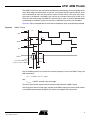
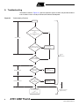
AT91x40 Series Board Design and
Troubleshooting Guide
1. Introduction
This document gives directions to hardware designers when designing a board based
on one of the AT91x40 microcontroller series and the AT91FR40x Flash-based products. The focus is on the verifications to be carried out at the board schematics level,
thus assuring the highest probability of a right-first-time system.
This board design checklist contains a Troubleshooting Guide which is highly recommended for reading when the first prototype board is powered up and if any
malfunction of the microcontroller is detected.
Note:
To facilitate usability of this application note, both the AT91x40 microcontroller series
and the AT91FR40x Flash-based products are referred to as the AT91x40x Series.
Words or sentences in bold highlight important points.
1.1
Abbreviation and Typographical Conventions
•
EBI: External Bus Interface
•
JTAG: Joint Test Action Group(1)
•
ICE: In-Circuit Emulator(1)
•
I/O pins: Any Input / Output pins
•
Gang Programmer: Automated Flash Programmer for High Volume Production
•
LSB: Last Significant Bit
•
MSB: Most Significant Bit
•
IBIS: Input/Output Buffer Information Specification
•
PCB: Printed Circuit Board
Note: 1.
AT91
ARM® Thumb®
Microcontrollers
Application
Note
As defined by the JTAG/ICE IEEE Std 1149 Standard.
All pin names prefixed with N (NOT), such as NRST and NWAIT for example, indicates an input or an output active low.
6151A–ATARM–15-Mar-05
1.2
Associated Documentation
Before going further into this document, it is recommended to check the latest documents for the AT91x40x Series on
Atmel's Web site.
Table 1-1 gives the associated documentation needed to support full understanding of this application note.
Table 1-1.
Product
AT91M40800
AT91R40008
AT91FR40162
AT91FR4042
2
Associated Documentation
Information
Document Title
User Manual
AT91x40 Series Full Datasheet
Internal architecture of processor
ARM/Thumb instruction sets
Embedded in-circuit-emulator
ARM7TDMI® Datasheet
Pinout Mechanical Characteristics
Ordering information
AT91M40800 Summary Datasheet
Timings DC characteristics
AT91M40800 Electrical Characteristics
User Manual
AT91x40 Series Full Datasheet
Internal architecture of processor
ARM/Thumb instruction sets
Embedded in-circuit-emulator
ARM7TDMI Datasheet
Pinout Mechanical Characteristics
Ordering information
AT91R40008 Summary Datasheet
Timings DC characteristics
AT91R40008 Electrical Characteristics
User Manual
AT91x40 Series Full Datasheet
Internal architecture of processor
ARM/Thumb instruction sets
Embedded in-circuit-emulator
ARM7TDMI Datasheet
Pinout Mechanical Characteristics
Ordering information
AT91R40008 Summary Datasheet
Flash Memory
AT49BV1614A Datasheet
Timings DC characteristics
AT91R40008 Electrical Characteristics
User Manual
AT91x40 Series Full Datasheet
Internal architecture of processor
ARM/Thumb instruction sets
Embedded in-circuit-emulator
ARM7TDMI Datasheet
Pinout Mechanical Characteristics
Ordering information
AT91R40008 Summary Datasheet
Flash Memory
AT49BV4096A Datasheet
Timings DC Characteristics
AT91R40008 Electrical Characteristics
AT91 ARM Thumb
6151A–ATARM–15-Mar-05
AT91 ARM Thumb
1.3
IBIS Models
For signal integrity analysis, IBIS Models for the AT91x40 Series are available from the Atmel
website.
For devices with embedded flash memory, IBIS Models do not include the IBIS model of the
flash memory.
1.4
Memory Size Summary
A summary of device memory sizes for the AT91x40x series is given in Table 1-2.
Table 1-2.
Device Memory Sizes
Product
Microcontroller
Internal SRAM
Internal Flash
AT91M40800
–
8K Bytes
–
AT91R40008
–
256K Bytes
–
AT91FR4042
AT91R40008
256K Bytes
AT49BV4096A
AT91FR40162
AT91R40008
256K Bytes
AT49BV1614A
2. Power Supply Pins
2.1
VDDCORE and VDDIO Pins
Table 2-1.
Power Supply Pins
Power Supply Pins
Voltage Range (Min/Nominal/Max) Function
VDDCORE(1)
See Electrical Datasheet
(1)
Powers the ARM7TDMI core, internal SRAM memory and
embedded peripherals.
VDDIO
Powers all I/O pads (GPIO and Peripheral dedicated pads).
GND
Common ground pin for VDDCORE, VDDIO and VPP.
Note: 1.
The power supply pins for the AT91M40800 are VDD.
The VDDCORE and VDDIO power supply rails must be connected to a clean DC source with a
decoupling capacitor as close as possible to the microcontroller's VDD/GND pins. Typical values
are 33 nF to 100 nF.
There are no particular constraints on these power supply pins during power sequencing, except
that the time-out delay of the reset circuit must cover the rising time of the two power supplies.
Note that due to internal level shifters, VDDIO cannot be stopped while VDDCORE is still provided to the microcontroller to save internal SRAM and register content, for example. Shutting
down VDDIO while VDDCORE is still on is not destructive but it can lead to unstable states on
the input of the internal peripherals. Moreover, except for ohmic loads in continuous domain
(LED, resistor bridge), the current consumption on VDDIO depends on the load capacitance
connected to the External Bus Interface I/O lines and the PIO lines when these lines are switching. This means that there is no need to shutdown the VDDIO power supply when the CPU is in
standby mode.
3
6151A–ATARM–15-Mar-05
2.2
VPP Pin
The VPP pin provides Flash Programming and Erasing Speed Enhancement. See the Flash
Memory Datasheet for voltage range to enable this speed enhancement. The VPP pin can be
left unconnected, but as an extra precaution, it is advised to put a known level on this pin to
avoid any external disruptive signal causing unwanted behavior.
3. Master Clock Pins
3.1
MCKI Pin
The MCKI pin is the Master Clock Input pin for the microcontroller. An external square wave
clock oscillator must be used in order to provide the internal clock source for the entire microcontroller. The High Half Period (tCH) and the Low Half Period (tCL) of the external oscillator
must have a minimum value as defined in the electrical datasheet. Connecting a crystal
only is not possible as there is no on-chip oscillator in the AT91x40x Series.
3.2
MCKO Pin
The Master Clock Output pin provides an image of the clock signal provided on the MCKI pin
with a delay to feed other devices in the system. The MCKO pin has a low drive capability, thus
making it not able to drive several TTL Loads. See the drive current capability in the corresponding product electrical datasheet. If this pin is not used, it is strongly advised to make it
available via a test point on the PCB when using one of the AT91x40x Microcontrollers in
a BGA Package. This will assure a quick verification as to whether or not the microcontroller
has a valid clock.
4. NRST Input Pin
The NRST pin is the Master System Reset. It is active low and resets all the internal peripheral
registers, the program counter of the ARM Core and the JTAG/ICE Port. It samples the signals
needed at boot-up such as the BMS and the NTRI pin. The NRST signal must be asserted until
all the power supplies provided to the microcontroller are stable and according to the startup
time of the external oscillator.
The NRST line must be held at level 0 for a minimum of 10 valid clock cycles before releasing
the NRST line to allow correct sampling of the BMS and the NTRI pins.
5. Sampled Pins during Reset
5.1
Boot Mode Select Pin (BMS)
This input pin, P25/BMS, is sampled on the rising edge of the NRST pin. This pin enables the
ARM7TDMI core to start fetching instructions from its internal flash memory, or from an external
memory, with one or the other connected to the Chip Select 0 (NCS0) of the EBI. Once the BMS
pin has been sampled during reset and the processor correctly initialized, the P25/BMS pin can
be used as general purpose I/O.
Depending on the data bus width of the memory chosen to boot from, 8 bits or 16 bits, the Boot
Mode Select pin (BMS) must be tied to a level 0 or a level 1. See the “Boot Mode Select” para-
4
AT91 ARM Thumb
6151A–ATARM–15-Mar-05
AT91 ARM Thumb
graph in the AT91x40 full datasheet, Atmel lit° 1345 for more details on the BMS pin
configuration.
5.2
Tri-State Input Pin
For debug purposes, the AT91x40x Series provides a tri-state mode. This enables the connection of an emulator probe to an application board without having to desolder the device from the
target board. In tri-state mode, all of the output pin drivers of the AT91x40x Series Microcontroller are disabled. For Flash based microcontrollers from the AT91FR40x Series, the tri-state
mode enables a gang programmer to treat the microcontroller like a standard Atmel Flash
memory.
The NTRI pin must be pulled up by a resistor of up to 400KΩ during the reset phase when
the user doesn't use the tri-state mode of the AT91. Note that the NTRI pin is multiplexed with
the I/O line P21 and the TXD1 line of the USART 1. If this line is connected to a standard RS232
driver, which generally contains an internal pull-up resistor of 400 KΩ, this pull-up resistor is not
required. See the specifications of the RS232 driver.
6. JTAG/ICE Port Pins
The TDI, TDO, TMS and TCK pins are the minimal pins found in any ARM Processor with a
JTAG/ICE Port as defined by the IEEE 1149 Standard. All pins except the TDO pin feature an
internal pull up resistor of approximately 10 KΩ.
These pins are used to access the In-Circuit-Emulator of the ARM Core for Debug purposes.
The AT91x40x Series does not feature Boundary-scan cells on digital IO's, thus making JTAG
Boundary-Scan Test Tools unusable with this family.
7. PIO Pins
7.1
Multiplexed Pins
Most of the I/O pins are multiplexed with one or two internal peripherals. Most of these pins have
their reset state in PIO mode, e.g. not driven by an internal peripheral, for example
P21/TXD1/NTRI. Some other pins like address lines A20 to A23 have their reset state in peripheral mode, e.g. driven by the EBI Controller. If those I/O pins, driven by a peripheral after the
reset, are not used, they can be used as general purpose I/O pins. See the paragraph “Peripheral Multiplexing on PIO Lines” in the full datasheet.
Unused PIO pins can be left unconnected but to avoid any external disruptive signal causing
unwanted behavior and/or internal pad oscillation resulting in an over current consumption, it is
advised to put those unused pins into output mode as soon as possible during the startup initialization code. No internal pull-up or pull-down resistors are embedded in the microcontroller on
these I/O lines.
7.2
PIO Only Pins
PIO only pins are I/O pins not multiplexed with any internal peripherals. By default, all I/O pins
are in input mode after the reset. Unused PIO pins can be left unconnected but to avoid any
external disruptive signal causing unwanted behavior and internal pad oscillation resulting in a
over current consumption, it is advised to turn those unused pins in output mode as soon as
5
6151A–ATARM–15-Mar-05
possible. No internal pull-up or pull-down resistors are embedded in the microcontroller on these
I/O lines
8. External Bus Interface Pins
8.1
Address Line Pins
The address bus of the AT91x40x Series has 24 address lines and thus can address up to
16M Bytes of memory space. Address lines A0 to A19 are not multiplexed with any PIO lines or
internal peripherals. Address lines A20 to A23 are multiplexed with PIO lines and with four additional chip select lines. If these four high address lines are not needed to access external
peripherals, they can be used as chip select lines or PIO lines. When one of the Flash Based
Microcontrollers from the AT91FR40x Series is used, note that the address line A20 must not be
use as a chip select line (CS7) or as a PIO line after reset. A20 is the MSB of the Internal Flash
memory.
8.2
Data Bus Pins
The data bus of the AT91x40x Series can be used in 8- or 16-bit mode, according to the state of
the BMS pin for the chip select 0 (NCS0) and according to the configuration of the EBI chip
select register for all the other chip select lines. Care must be taken that microcontrollers from
the AT91x40x Series do not embed internal pull-up or pull-down resistors on the data bus. It is
strongly advised to add pull-up or pull-down resistors of 100 KΩ to avoid any external disruptive
signal causing unwanted behavior and/or internal pad oscillation resulting in a over current consumption on both VDDCORE and VDDIO. The maximum load capacitance which can be driven
by the data bus can be evaluated by using the AT91 External Bus Interface Timing Calculator
Application Note (literature° 2620) available from the AT91 CD-ROM or from the Atmel website.
8.3
Control Signal Pins
The Control Bus is made of several read and write lines, chip select lines and byte select lines
which enable the user to connect a wide variety of memories and peripherals. Care must be
taken around the maximum load capacitance acceptable on the NWR and NRD lines according
to the master clock of the microcontroller. Overloading the NWR line and the NRD line may
extend some EBI timings, resulting in inconsistent read or write accesses.
The maximum load capacitance that can be driven by the control bus signals can be evaluated
by using the AT91 External Bus Interface Timing Calculator Application Note (literature° 2620)
available from the AT91 CD-ROM or from the Atmel website.
8.4
NWAIT Pin
The NWAIT pin adds extra wait state cycles for read or write accesses when programmable
standard wait states are not enough or at any time during the access. When NWAIT is detected
low, the core clock is stopped and the EBI stops the current access but it does not change the
output signals nor its internal counter and state. When NWAIT is de-asserted, the core clock is
released and the EBI finishes the access sequence.
The NWAIT pin is an active low input and detected on the rising edge of the master clock. The
NWAIT input signal can only be asserted synchronously during the low period of the
master clock (MCK).
6
AT91 ARM Thumb
6151A–ATARM–15-Mar-05
AT91 ARM Thumb
The NWAIT signal must also meet setup and hold timing requirements on the rising edge of the
clock. When setup and hold timings are not met, it may freeze the EBI signals into their active
state immediately (or even after some access cycles) and will remain in this state until a hardware reset is performed. If the NWAIT pin is driven by an external device like a DSP or an
FPGA, the user must ensure that NWAIT pin is driven high as soon as the AT91 Microcontroller
is powered-up. If the NWAIT input pin is not used, a 100 KΩ pull up resistor must be added.
Figure 8-1 and its associated formula show how to compute the setup and hold timings required.
Figure 8-1.
NWAIT Timings
tCP/2
MCKI
tCDHL
tCDHL
MCKO
EBI 4
NCS
EBI 5
NWAIT
These dashed lines show
possible assertion of NWAIT
EBI 6
tNWAIT
Use the following formula to calculate the maximum frequency to reach the NWAIT setup and
hold requirements.
T CP ⁄ 2 > EBI4 + T NWAIT – EBI5
with:
T NWAIT = NWAIT assertion after falling edge.
This time is given by the response time of the device which drives the NWAIT signal.
The image of the internal master clock available on the MCKO output pin can be used to achieve
a resynchronization between the NWAIT pin and the rising edge of the master clock.
7
6151A–ATARM–15-Mar-05
9. Troubleshooting
The flowchart shown in Figure 9-1 gives the important signals to check and possible trouble to
avert in order to assure a ready-to-run board for software development.
Figure 9-1.
Troubleshooting Flowchart
Power Up
VDDCORE/VDDIO rising time
vs.
reset time
vs.
External OSC startup time
OK?
NO
Time Restricted
YES
10 valid clock cycles on
MCKI before NRST Rising?
NO
The microcontroller will
not start or will be
wrongly initialized.
YES
Power up
and
Reset Phase
Image of MCKI
available on MCKO Pin?
NO
YES
Mandatory Pin Level
NWAIT and NTRI
Pulled High?
NO
The micrcocontroler
will not start or
will start in Tri-State mode.
NO
The micrcocontroler will
not execute the
initialization code.
YES
User Defined Pin Level
NRST
YES
Microcontroller is ready
to run the application
code
(Cstartup, C code)
8
Rising Edge on
Correct BMS Level
vs.
Data Bus Width
Initialization and User's
Application Phase
AT91 ARM Thumb
6151A–ATARM–15-Mar-05
AT91 ARM Thumb
10. Revision History
Table 10-1.
Revision History
Doc. Rev
Date
Comments
6151A
21-Feb-05
23-Feb-05
First issue
Unqualified / Internal on Intranet
Change Request Ref.
9
6151A–ATARM–15-Mar-05
Atmel Corporation
2325 Orchard Parkway
San Jose, CA 95131, USA
Tel: 1(408) 441-0311
Fax: 1(408) 487-2600
Regional Headquarters
Europe
Atmel Sarl
Route des Arsenaux 41
Case Postale 80
CH-1705 Fribourg
Switzerland
Tel: (41) 26-426-5555
Fax: (41) 26-426-5500
Asia
Room 1219
Chinachem Golden Plaza
77 Mody Road Tsimshatsui
East Kowloon
Hong Kong
Tel: (852) 2721-9778
Fax: (852) 2722-1369
Japan
9F, Tonetsu Shinkawa Bldg.
1-24-8 Shinkawa
Chuo-ku, Tokyo 104-0033
Japan
Tel: (81) 3-3523-3551
Fax: (81) 3-3523-7581
Atmel Operations
Memory
2325 Orchard Parkway
San Jose, CA 95131, USA
Tel: 1(408) 441-0311
Fax: 1(408) 436-4314
RF/Automotive
Theresienstrasse 2
Postfach 3535
74025 Heilbronn, Germany
Tel: (49) 71-31-67-0
Fax: (49) 71-31-67-2340
Microcontrollers
2325 Orchard Parkway
San Jose, CA 95131, USA
Tel: 1(408) 441-0311
Fax: 1(408) 436-4314
La Chantrerie
BP 70602
44306 Nantes Cedex 3, France
Tel: (33) 2-40-18-18-18
Fax: (33) 2-40-18-19-60
ASIC/ASSP/Smart Cards
1150 East Cheyenne Mtn. Blvd.
Colorado Springs, CO 80906, USA
Tel: 1(719) 576-3300
Fax: 1(719) 540-1759
Biometrics/Imaging/Hi-Rel MPU/
High Speed Converters/RF Datacom
Avenue de Rochepleine
BP 123
38521 Saint-Egreve Cedex, France
Tel: (33) 4-76-58-30-00
Fax: (33) 4-76-58-34-80
Zone Industrielle
13106 Rousset Cedex, France
Tel: (33) 4-42-53-60-00
Fax: (33) 4-42-53-60-01
1150 East Cheyenne Mtn. Blvd.
Colorado Springs, CO 80906, USA
Tel: 1(719) 576-3300
Fax: 1(719) 540-1759
Scottish Enterprise Technology Park
Maxwell Building
East Kilbride G75 0QR, Scotland
Tel: (44) 1355-803-000
Fax: (44) 1355-242-743
Literature Requests
www.atmel.com/literature
Disclaimer: The information in this document is provided in connection with Atmel products. No license, express or implied, by estoppel or otherwise, to any
intellectual property right is granted by this document or in connection with the sale of Atmel products. EXCEPT AS SET FORTH IN ATMEL’S TERMS AND CONDITIONS OF SALE LOCATED ON ATMEL’S WEB SITE, ATMEL ASSUMES NO LIABILITY WHATSOEVER AND DISCLAIMS ANY EXPRESS, IMPLIED OR STATUTORY
WARRANTY RELATING TO ITS PRODUCTS INCLUDING, BUT NOT LIMITED TO, THE IMPLIED WARRANTY OF MERCHANTABILITY, FITNESS FOR A PARTICULAR
PURPOSE, OR NON-INFRINGEMENT. IN NO EVENT SHALL ATMEL BE LIABLE FOR ANY DIRECT, INDIRECT, CONSEQUENTIAL, PUNITIVE, SPECIAL OR INCIDENTAL DAMAGES (INCLUDING, WITHOUT LIMITATION, DAMAGES FOR LOSS OF PROFITS, BUSINESS INTERRUPTION, OR LOSS OF INFORMATION) ARISING OUT
OF THE USE OR INABILITY TO USE THIS DOCUMENT, EVEN IF ATMEL HAS BEEN ADVISED OF THE POSSIBILITY OF SUCH DAMAGES. Atmel makes no
representations or warranties with respect to the accuracy or completeness of the contents of this document and reserves the right to make changes to specifications
and product descriptions at any time without notice. Atmel does not make any commitment to update the information contained herein. Atmel’s products are not
intended, authorized, or warranted for use as components in applications intended to support or sustain life.
© Atmel Corporation 2005. All rights reserved. Atmel®, logo and combinations thereof and others are registered trademarks, and Everywhere
You Are SM and others are trademarks of Atmel Corporation or its subsidiaries. ARM ® ARM7TDMI®, Thumb ® and the ARM Powered ® logo are registered trademarks of ARM Limited. Other terms and product names may be trademarks of others.
Printed on recycled paper.
6151A–ATARM–15-Mar-05