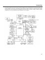
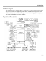
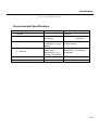
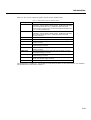
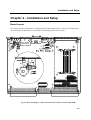
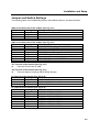
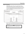
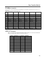
1
 XVME-6200
6U VME Intel® Core™ 2 Duo Processor Board
USER’S MANUAL
ACROMAG INCORPORATED
30765 South Wixom Road
P.O. BOX 437
Wixom, MI 48393-7037 U.S.A.
Tel: (248) 295-0885
Fax: (248) 624-9234
Email: [email protected]
Copyright 2012, Acromag, Inc., Printed in the USA.
Data and specifications are subject to change without notice.
8500-980D Revision
A
B
C and D
Description
Init
Updates
Updates
Date
11/07
06/08
07/10
Part Number 746200
Trademark Information
Brand or product names are trademarks or registered trademarks of their respective owners.
Intel and Pentium are registered trademarks and Celeron is a trademark of Intel Corporation.
Windows, Windows 2000 and Windows XP are registered trademarks of Microsoft Corporation
in the US and in other countries.
Copyright Information
This document is copyrighted by Xembedded, Incorporated (Xembedded) and shall not be
reproduced or copied without expressed written authorization from Xembedded.
The information contained within this document is subject to change without notice. Xembedded
does not guarantee the accuracy of the information.
WARNING
This is a Class A product. In a domestic environment this product may cause radio interference,
in which case the user may be required to take adequate measures.
Warning for European Users – Electromagnetic Compatibility
European Union Directive 89/336/EEC requires that this apparatus comply with relevant ITE
EMC standards. EMC compliance demands that this apparatus is installed within a VME
enclosure designed to contain electromagnetic radiation and which will provide protection for the
apparatus with regard to electromagnetic immunity. This enclosure must be fully shielded. An
example of such an enclosure is a Schroff 7U EMC-RFI VME System chassis, which includes a
front cover to complete the enclosure.
The connection of non-shielded equipment interface cables to this equipment will invalidate
European Free Trade Area (EFTA) EMC compliance and may result in electromagnetic
interference and/or susceptibility levels that are in violation of regulations which apply to the
legal operation of this device. It is the responsibility of the system integrator and/or user to apply
the following directions, as well as those in the user manual, which relate to installation and
configuration:
All interface cables should be shielded, both inside and outside of the VME enclosure.
Braid/foil type shields are recommended for serial, parallel, and SCSI interface cables.
Where as external mouse cables are not generally shielded, an internal mouse interface
cable must either be shielded or looped (1 turn) through a ferrite bead at the enclosure
point of exit (bulkhead connector). External cable connectors must be metal with metal
back-shells and provide 360-degree protection about the interface wires. The cable shield
must be terminated directly to the metal connector shell; shield ground drain wires alone
are not adequate. VME panel mount connectors that provide interface to external cables
(e.g.,
ii
RS232, USB, keyboard, mouse, etc.) must have metal housings and provide direct
connection to the metal VME chassis. Connector ground drain wires are not adequate.
Environmental Protection Statement
This product has been manufactured to satisfy environmental protection requirements where
possible. Many of the components used (structural parts, printed circuit boards, connectors,
batteries, etc.) are capable of being recycled.
Final disposition of this product after its service life must be accomplished in accordance with
applicable country, state, or local laws or regulations.
iii
Table of Contents
Table of Contents
XVME-6200................................................................................................................................. i
Table of Contents ................................................................................................................................ v
Table of Figures ................................................................................................................................ vii
Chapter 1 – Introduction ....................................................................................................... 1-1
Module Features ............................................................................................................................ 1-1
Architecture ................................................................................................................................... 1-2
XVME-6200 Memory Map............................................................................................................ 1-4
XVME-6200 I/O Map.................................................................................................................... 1-5
Interrupt Usage .............................................................................................................................. 1-6
Software Support ......................................................................................................................... 1-10
Operational Description .............................................................................................................. 1-12
Environmental Specifications....................................................................................................... 1-13
Hardware Specifications .............................................................................................................. 1-14
VMEbus Specification ................................................................................................................. 1-15
System Configuration and Expansion Options Tables................................................................... 1-15
Chapter 2 – Installation and Setup....................................................................................... 2-1
Jumper and Switch Settings ........................................................................................................... 2-2
Jumper and Switch Settings ........................................................................................................... 2-3
Registers........................................................................................................................................ 2-4
Front Panel Layout......................................................................................................................... 2-6
Connectors..................................................................................................................................... 2-7
COM1 and COM3 (J4) Pin Definitions........................................................................................... 2-11
Figure 2-11 RJ-45 Serial Port Connector ........................................................................................ 2-11
VMEbus P2 Connector................................................................................................................... 2-14
Table 2-17 VMEbus P2 Connector ................................................................................................. 2-15
Installing the XVME-6200 into a Backplane ................................................................................ 2-19
Enabling the PCI Ethernet Controller ........................................................................................... 2-20
Chapter 3 BIOS Setup Menus............................................................................................... 3-1
Chapter 4 Programming........................................................................................................ 4-1
Memory Map................................................................................................................................. 4-1
I/O Map ......................................................................................................................................... 4-1
IRQ Map ....................................................................................................................................... 4-3
PCI Device Map -............................................................................................................................. 4-4
VME Interface ............................................................................................................................... 4-5
Software-Selectable Byte-Swapping Hardware............................................................................... 4-7
Chapter 5 XVME-990 Rear Transition Module ..................................................................... 5-1
Connectors..................................................................................................................................... 5-2
Serial ATA hard drive Interface ..................................................................................................... 5-3
v
Table of Contents
Appendix A .............................................................................................................................. 1
Memory Type ................................................................................................................................... 1
Installing SDRAM ............................................................................................................................ 1
Module Battery Installation............................................................................................................... 1
Index................................................................................................................................................... 2
vi
Table of Contents
Table of Figures
Figure 1-1 XVME-6200 Block Diagram.................................................................................1-13
Figure 4-1 Byte Ordering Schemes...........................................................................................4-8
Figure 4-2 Address-Invariant Translation .................................................................................4-8
Figure 4-3 Maintaining Numeric Consistency...........................................................................4-9
Figure 4-4 Maintaining Address Consistency..........................................................................4-10
Figure 5-1 XVME-990/X Installation (XVME-990-001 shown) ...............................................5-1
vii
Introduction
Chapter 1 – Introduction
The XVME-6200 VMEbus Intel® Core2tm Duo and Core Duo PC-compatible VMEbus processor module
combines the high performance and ruggedized packaging of the VMEbus with the broad application software
base of the IBM PC/AT standard. It integrates the latest processor and chipset technology. The only difference
between the various versions of the XVME-6200 is the CPU used. The L7400 is the lowest power draw of any
of our processors while maintaining a very high level of processing power. The T7400 offers the highest
performance.
Module Features
The XVME-6200 offers the following features:
•
•
•
•
•
•
•
•
•
•
•
•
•
•
•
•
•
•
Intel® Core2tm Duo Processor. All processor models can be configured with 1GB to 8GB SDRAM
(show as total memory on board).
Level 2 cache on Intel® Core2tm Duo is 4MB (T7400 and L7400).
Video controller with 4MB of VRAM. (Silicon Motion 722)
Enhanced IDE controller, capable of driving two EIDE devices on P2 (Compatible with XVME-977
Hard drive/Floppy drive unit and XVME-979 Hard Drive/DVD-CDROM drive unit)
Two channels of SATA-150 out P2. Use the XVME-990 to provide the connectors needed to
connect external SATA drives.
Floppy disk controller, capable of driving one floppy drive on P2 (Compatible with XVME-977
Hard drive/Floppy drive unit or XVME-979 CD-ROM/DVD drive and Hard Drive with external
drive)
Dual 10/100/1000 Base T Ethernet controllers with front panel RJ-45 connectors with isolated
ground or selectable out the P0 to support rear Ethernet or Vita 31.1.
Type I/II Compact Flash site using our XVME-912 optional carrier. This mounts in the PMC site
and does not allow for a PMC module to be used.
On-Board Hard Drive using our XVME-913 1.8” hard drive. This mounts in the PMC site and does
not allow for a PMC module to be used.
VME64X VMEbus interface with programmable hardware byte swapping
Support for Vita 31.1 Switch Fabric in complaint back planes
Three serial ports:
• One RS-232 serial port on front panel (Com 1) with electrical isolation (Com port 1 can be
configured for RS-232/422/485)
• One RS-232 serial port (Com 2 ) on P2 (use our XVME-990 to access)
Four Universal Serial Bus (USB 2.0) ports 1 and 2 on front and 3 and 4 out P2. (use our XVME-990
to access)
EPP/ECP configurable parallel port (P2) on 26-pin header on the XVME-990
Combined PS/2 compatible keyboard/mouse port on front panel. Use USB for rear keyboard/mouse.
PCIe 38-pin Expansion Connector (NOT Compatible with XVME-976-01 thru XMVE-976-205
Carriers) must use the XVME-9076.
PMC (PCI Mezzanine Card) site with front panel I/O 32/64-bit 33/66MHz with rear I/O using
optional P0 connector. This site is on the internal PCI-X bus.
Front panel ABORT/RESET switch with indicating lights. Red for “fail” and green for “pass”
1-1
Introduction
•
•
•
Electrical isolation and noise immunity on the Ethernet ports, Serial Port, and PMC site.
Ejector type handles in IEEE 1101.10 (Compact PCI type) or IEEE 1101.1 (legacy VME type).
VME64 VMEbus interface with programmable hardware byte swapping
Architecture
CPU Chip
The Intel® Core2tm Duo processors have a new micro-architecture, but remains software compatible with
previous members of the Intel microprocessor family. The Intel® Core2tm Duo has a 4MB L2 cache which
boosts performance. The two cores can run independent processes, potentially doubling performance. With
a junction temperature range of 0 to 100C, the Intel® Core2tm Duo processors are capable of with standing
a great deal of thermal stress. The 17 watt L7400 Intel® Core2tm Duo 1.5Ghz processors provide low power
options and T7400 Intel® Core2tm Duo 2.16GHz processor provide higher performance options.
PCI Local Bus Interface
The Intel E7520 / 6300ESB chipset supports the Intel® Core2tm Duo processors with up to 400MHz front
side bus. The XVME-6200 incorporates one PCIe and PCI-X buses which is used to service the two Intel
82546EB Ethernet controllers and the on-board PMC site. The PMC site supports both 32-bit/33MHz and
64-bit/66MHz bus speeds with 5V I/O support. The XVME-6200 supports on PCI bus for 32-bit/33MHz
operation, this bus services the PCI to VME bridge chip known as the tundra Universe II chip and the 38pin expansion connector used to connect to the XVME-9076 Dual PMC carrier module.
PCI-X, or PCI extended, is an enhanced version of PCI (Peripheral Component Interconnect) computer
bus. Although PCI-X is backward-compatible with traditional 3.3V PCI 2.0 devices and systems, this
specification implements additional features and performance improvements include 3.3V signaling,
increased speed grades, and adaptation to other form factors. PCI-X effectively doubles the speed and
amount of data exchanged between the computer processor and peripherals. PCI-X bus was designed for
and is ideally suited for server cards such as Fibre Channel, RAID, high-speed networking, and other
demanding devices.
Onboard Memory
SDRAM Memory
The XVME-6200 is configured with “dual channel” memory, each CPU core has it’s own path to the
memory modules. The two memory sockets are 200-pin SODIMM, providing 512MB, 1GB, 2GB and
4GB of ECC DDR 466MHz SDRAM. Approved SDRAM suppliers are listed in 0.
Flash BIOS
The XVME-6200 system BIOS is contained in a 1MB flash device to facilitate system BIOS updates.
Contact Xembedded support for available updates at [email protected] if needed. Be sure to record
your current version number and the reason for the request.
Video Controller
The Silicon Graphics 722 graphics controller has a built-in 2D/3D. The maximum video modes supported are listed
in the following table. The highest supported interlaced monitor mode is 1280x1024, 16-bit/65k color, and 43 Hz.
Video output is available on the front panel through a standard 15-pin D shell connector. The 722 graphics
1-2
Introduction
controller uses up to 128MB of on-board video memory. The SG 722 has a built-in 3D graphics engine and its
display / render core frequency is up to 200MHz.
Table 1-1 Maximum Video Modes
Supported Resolution
640x480
800x600
1024x768
1280x1024
1600x1200
Bit Depth/Colors
Vertical Refresh
24-bit/16M color
24-bit/16M color
24-bit/16M color
24-bit/16M color
16-bit/65k color
100 Hz
100 Hz
100 Hz
75 Hz
60 Hz
Ethernet Controller
The 82571EB dual Giga-bit Ethernet controller provides a pair of 10/100/1000baseT Ethernet interfaces. The
82571EB contains both the MAC and the physical layer. The RJ-45 connectors on the module's front panel provide
auto-sensing for 10Base-T, 100Base and 1000Base -TX connections. Each RJ-45 connector has two indicator lights.
When mounted vertically, the top light is the link/activity light and the bottom light (the one closer to the COM
ports) is the 10Base-T/100Base-TX indicator. When it is off, the connection is 10Base-T; when it is on, the
connection is 100Base-TX. When the Ethernet is switched to the rear optional P0 no lights are available to indicate
link or speed. The use of the XVME-990 is required to connect RJ-45 cables to the rear of the XVME-6200
processor boards.
Memory Layout
Basic Memory Regions
There are five basic regions of memory in the system: memory below 1 MB, memory between
1 MB and the Top of Low Memory (TOLM) register memory between the TOLM register and 4 GB, memory above 4
GB, and the high PCI memory range between the top of main memory and 64 GB. The high PCI memory range is added
with the MCH, and was not available in previous generations of Intel Architecture 32-bit MCHs.
Note that the DRAM that physically overlaps the low PCI Memory Address Range (between TOLM and the 4-GB
boundary) may be recovered for use by the system. For example, if there is 4 GB of physical DRAM and 1 GB of PCI
space, then the system can address a total of 5 GB. In this instance the top GB of physical DRAM physically located
from 3 GB to 4 GB is addressed between 4 GB and 5 GB by the system.
1-3
Introduction
XVME-6200 Memory Map
The memory map of the XVME-6200 as seen by the CPU is shown below. The I/O designation refers to memory which
is viewed as part of the AT bus or as part of VMEbus depending on how the Universe is programmed.
XVME-6200 MEMORY MAP
ADDRESS RANGE
(HEX)
FFFC0000 - FFFFFFFF
end of DRAM -FFFBFFFF
00100000 – end of DRAM
000F0000 – 000FFFFF
000E0000 – 000EFFFF
000D8000 – 000DFFFF
SIZE
DEVICE
256K
xxxK
xxxK
64K
64K
32K
SYSTEM BIOS
I/O MEMORY**
DRAM *
SYSTEM BIOS
SYSTEM BIOS
Universe Real Mode
Window
000D0000 – 000D7FFF
32K
Open memory block
000CC000 – 000CFFFF
16K
Open memory block
000C0000 – 000C7FFF
32K
VGA BIOS
000A0000 – 000BFFFF
128K
VGA DRAM MEMORY
00000000 – 0009FFFF
640K
DRAM
*See Intel 6300ESB data sheet for description for optional settings for memory holes or gaps within Memory map area
**The PCI devices are located at the very top of memory just below the system BIOS.
1-4
Introduction
XVME-6200 I/O Map
I/O map for the XVME-6200 contains I/O ports of the IBM AT architecture plus some additions for PCI I/O registers
and Xycom specific I/O registers.
Hex Range
000-01F
020-021
022-023
024-02D
02E-02F
030-03D
040-042
043
04E-04F
050-052
060-06F
070-07F
080-091
92
93-9F
0A0-0B1
0B2-0B3
0B4-0BF
0C0-0DF
0F0
0F1
0F2-0FF
170-177
1F0-1F7
219
234
235-277
278-27F
280-2F7
2F8-2FF
300-36F
376
378-37F
380-3BF
3C0-3DF
3E8-3EF
3F0-3F5
3F6
3F8-3FF
4D0h
4D1h
CF8
CF9
Device
DMA controller 1, 8237A-5 equivalent
Interrupt controller 1, 8259 equivalent
Available
Interrupt controllers
LPC SIO
More interrupt controllers
Timer/Counter, 8254-2 equivalent
Timer/Counter (write only)
LPC SIO
Timer/Counter
8742 equivalent (keyboard)
Real Time Clock bit 7 NMI mask
DMA page register
Fast GateA20 and Fast CPU Init
DMA page register
Interrupt controller 2, 8259 equivalent
Power Management
Interrupt controller 2, 8259 equivalent
DMA controller 2, 8237A-5 equivalent
FERR#/IGNNE#/Interrupt Controller
N/A
N/A
Secondary IDE Controller (Generates CS1*)
Primary IDE Controller (Generates CS1*)
Xycom LED control register
Byte Swap, LAN select, Video select port
Available
Parallel Port 2
Available
COM2 Serial Port
Available
Secondary IDE Controller (Generates CS3*)
Parallel Port 1
Available
VGA/EGA2
COM3 Serial Port
Primary Floppy disk controller
Primary IDE Controller (Generates CS3*)
COM1 Serial port
ELCR1 (Edge or level triggered)
ELCR2 (Edge or level triggered)
PCI configuration address register
Reset Control Register
1-5
Introduction
CFC
PCI configuration data register
Interrupt Usage
INT#
IRQ0
IRQ1
IRQ2
IRQ3
IRQ4
IRQ5
IRQ6
IRQ7
IRQ8
IRQ9
IRQ9
IRQ10
IRQ11
IRQ12
IRQ13
IRQ14
IRQ15
Function
System Timer
Keyboard
Interrupt Cascade (reserved)
COM2
COM1
Floppy
Parallel Port (LPT1)
Real Time Clock
Universe IID
Video
Onboard PMC-X
Ethernet 1 and 2
Mouse
Math Coprocessor (reserved)
Primary IDE
Secondary IDE
The above interrupt mapping is one possible scenario. The user or operating system may choose a different mapping for
some of these interrupts based on what devices are actually in the system and require interrupts. If COM2 or LPT1 are
not used, then these would free up IRQ3 and IRQ7 respectively. Only one of COM1 or COM3 can function at a time
since IRQ4 is edge triggered.
The default BIOS has the following settings.
Interrupt Processing
[Use APIC]
MP Tables
[Enabled]
Storage Devices (Hard Drive, Floppy, Compact PCI and On-Board Drive)
EIDE and Floppy Drives
The XVME-6200 primary IDE and floppy drive signals are routed through the P2 connector inner three rows
(available in a legacy 96-pin back plane), providing a simplified method of connecting up to two IDE devices and
one external floppy drive. The secondary IDE master signals support the optional on-board hard drive or on-board
Compact Flash site and the secondary IDE slave signals are not supported.
When used with the XVME-977 and/or the XVME-979 mass storage modules, the IDE devices and floppy drives
do not need to be located next to the processor. Using the supplied six-inch ribbon cable (which connects the
XVME boards' J2 VME backplane connectors), the XVME-977 or the XVME-979 can be installed up to four slots
away from the XVME-6200 on the VME backplane. This allows greater flexibility in configuring the VMEbus card
cage.
1-6
Introduction
For applications that require mass storage outside the VMEbus chassis, the XVME-990 rear transition module plugs
onto the VMEbus J2 connector. This module provides industry standard connections for IDE and floppy signals.
One floppy drive can be connected to the XVME-990. This drive may be 2.88 MB, 1.44 MB, 1.2 MB, or 720 KB,
360 KB in size. For more information on the XVME-990, refer to Chapter 5.
1-7
Introduction
Caution
The IDE controller supports enhanced PIO modes, which reduce the cycle times for
16-bit data transfers to the hard drive. Check with your drive manual to see if the drive
you are using supports these modes. The higher the PIO mode, the shorter the cycle
time. As the IDE cable length increases, this reduced cycle time can lead to erratic
operation. As a result, it is in your best interest to keep the IDE cable as short as
possible.
The PIO modes can be selected in the BIOS setup. The Auto configuration will attempt
to classify the connected drive if the drive supports the auto ID command. If you
experience problems, change the Transfer Mode to Standard.
Caution
The total cable length must not exceed 18 inches. Also, if two drives are connected, they
must be no more than six inches apart. See SATA below for longer cable lengths.
Serial ATA Hard Drive
The XVME-6200 features two (2) SATA-150 drive interfaces out the rear P2 VMEbus connector. The use of the
optional rear transition module (XVME-990) allows for the connection of two drives using standard SATA
cables. If your application requires the external drives to be mounted in a location that requires a long cable run,
the SATA drives are better suited to that application. SATA cable can be up to 1 meters or 39” long, EIDE have
be less than 18” long.
Serial ATA – 7-pin connector
The 0.5” wide cable connector directly connects the 4 signal wires and 3 ground lines to the receiving terminal in
a single row. Because the connector includes the shielding ground pins, very little crosstalk is introduced. Note
that the receiving terminal uses extended connectors for the 3 ground signals so that the ground reference
between the device and host can be shared prior to signals being applied at the input. A similar mating sequence
is enforced with the new 7/8” wide 15-pin single row power connector. This feature is necessary to
accommodate hot-plugging. The 7-pin plugs from both channels of the SATA-150 are on the XVME-990, the
use of this rear transition module make it possible to connect to a SATA drive. Contact www.serialata.org for
more information on the SATA interface.
On-Board Hard Drive (Optional module XVME-913)
The on-board hard drive resides as a master on the secondary EIDE port. The XVME-913 is a kit of parts
including; 1.8” hard drive, cable, 4 brackets, screws and standoffs. There are no unique drivers required. The
XVME-6200 can be booted from the on-board hard drive if configured in the BIOS Boot menu. NOTE: The
XVME-6200 module can accept either an on-board 1.8” hard drive (XVME-913) or the Compact Flash
carrier (XVME-912) but not both.
Compact Flash Site (Optional module XVME-912)
The compact flash socket on the optional carrier module will support type I or type II Compact Flash cards. The
compact flash resides as a master on the secondary IDE port. There are no unique drivers required. The XVME6200 can be booted from the compact flash drive if configured in the BIOS Boot menu. NOTE: The XVME6200 module can accept either an on-board 1.8” hard drive (XVME-913) or the Compact Flash carrier
(XVME-912) but not both.
1-8
Introduction
VMEbus Interface
The XVME-6200 uses the PCI local bus to interface to the VMEbus via a PCI to VME bridge device (Tundra Universe
IID). The VMEbus interface supports full DMA to and from the VMEbus, integral FIFOs for posted writes, block mode
transfers, and read-modify-write operations. The interface contains one master and eight slave images that can be
programmed in a variety of modes to allow the VMEbus to be mapped into the XVME-6200 local memory. This makes it
easy to configure VMEbus resources in protected and real mode programs The XVME-6200 also incorporates onboard
hardware byte-swapping (see Table 1-2). For a complete API, the Xembedded Board Support Packages tailored to your
operating system will allow quick programming of your application.
Serial and Parallel Ports
XVME-6200 includes three high-speed 16550-compatible serial ports (RS-232C) with Com 1 capable of RS-232 and RS422/485 configurations. The Parallel port can be configured for ECP or EPP parallel port. This is done in the SMC
SCH3114 LPC Super I/O and programmed via the BIOS. Com ports 1 and 3 are RJ-45’s on the front panel and Com2 is
available out the P2 VMEbus connector and requires the use of the XVME990 which provides a standard DB-9
connection.
Keyboard / Mouse Interface
A combined keyboard and mouse port PS/2 connector is provided on the front panel. A PS/2 splitter cable part number
140232 (provided with the module) may be used to separate the two ports so that both devices may be simultaneously
connected to the module. IF a mouse is not required, a keyboard can be connected directly to the PS/2 port. The keyboard
and mouse are controlled in the SMC SCH3114 LPC Super I/O.
PMC Expansion
The XVME-6200 provides an on-board PMC site for use with standard 32/64-bit, 33/66MHz PMC and PMC-X modules.
The PMC site is serviced by the on-board PCI-X bus. For electrical isolation, the PMC front panel bezel is not connected
to the main CPU ground. PCI-X, or PCI extended, is an enhanced version of PCI (Peripheral Component Interconnect)
computer bus. Although PCI-X is backward-compatible with traditional PCI devices and systems, this specification
implements additional features and performance improvements include 3.3V signaling, increased speed grades, and
adaptation to other form factors. PCI-X effectively doubles the speed and amount of data exchanged between the
computer processor and peripherals. PCI-X bus was designed for and is ideally suited for server cards such as FPGA,
DSP, Fibre Channel, RAID, high-speed networking, and other demanding devices. If a standard PCI PMC card is fitted on
the XVME-6200 PMC site, the on-board PCI-X bus reverts to the PCI bus speed.
Additional PMC Expansion Options
The XVME-6200 supports optional PMC (PCI Mezzanine Card) expansion using XVME-9076 expansion module. The
XVME-9076 provides two PCI Mezzanine Card (PMC) sites. The XVME-9076 module is designed to plug directly into
the XVME-6200 using the 38-pin expansion board connector.
1-9
Introduction
Watchdog Timer
The XVME-6200 has a long duration watchdog timer which can count from 1 to 255 seconds or from 1 to 255 minutes.
The BIOS supports various system events which can be routed to the watchdog timer. The timer when enabled can
generate either an interrupt or a master reset depending on how the watchdog timer is configured.
Note
The timeout range is from 1.0 second to 2.25 seconds; it will typically be 1.6 seconds.
USING THE WATCHDOG Timer
The xvme6200 has a watchdog function on the Intel 6300ESB (alias ICH or Southbridge). The output of the watchdog
function is the WDT_TOUT pin. For this feature to work you must first have the correct PLD firmware loaded on the
xvme6200 since WDT_TOUT goes through the PLD to drive system reset. If you are in doubt about the state of this PLD
logic contact Xembedded (only Xembedded can update this firmware).
For specifics of the watchdog of the xvme6200 see the "Intel® 6300ESB I/O Controller Hub" datasheet from Intel. There
are multiple modes and various configurations. This description only discusses the 'free-running' mode and how it was
tested using a PCI debug tool called PCIscope (http://www.tssc.de/index.htm#). PCIscope has a debugger that let's the
user interactively read/write to PCI config registers and memory mapped locations (hence the commands below). Of
course any debugger could do the same.
Following is a high level description of what your watchdog application/driver would need to do to utilize the watchdog
in free-running mode :
Initially your application needs to get PCI bus:dev:fun of 6300ESB watchdog. Device ID is 25ABh. In our example
below PCI bus:dev:fun is 00:1d:04:nn where nn=offset. The Preload2 register is memory mapped at Offsetbase + 04h so
the app needs to know what this is too via the PCI config space of the device (our system was at D7EF_E7F0).
1) When application initially comes up it should check to see if the system was reset due to a previous watchdog event.
There is a persistent status bit that gets saved in the 6300's RELOAD register (section 16.4.21 of Intel doc, OffsetBase +
0Ch). This bit is WDT_TIMEOUT. It will remain set between resets (not hard power-down though). So this bit should be
checked. If it is set then it needs to be cleared using the 'register unlocking sequence' (see code below, it's three separate
commands in a specific order).
2) Load timeout value into Preload2 counter. By default this is a 1kHz clock so each tick is 1msec. In our example code
below we load a value of 0AAAAh into preload2. This is equivalent to 43,690 (decimal) therefore 43.69 seconds.
3) Enable free-running mode and enable watchdog via offset 68h and WDT_TOUT_CNF and WDT_ENABLE bits. The
counter loaded with preload2 value immediately starts counting down.
4) To prevent watchdog from tripping you disable/enable watchdog again. Every time you do this it automatically
reloads value from preload2 and starts counting down again.
1-10
Introduction
Commands for Watch Dog Timer in PCIscope
THESE ARE THE COMMANDS USED TO RUN IN FREE_RUNNING MODE (from PCIscope)
----------------------------------------------------------------------1) To check WDT_TIMEOUT to see if previous WDT occurred. If == 0200 you need to 'unlock'
DW D7EFE7FC
** The next command is a macro that writes to the Offset Base address (in our case D7EFE7F0) + 0Ch
** to perform the 'register unlocking sequence', writing commands of 80h & 86h consecutively,
** then it writes to WDT_TIMEOUT (bit 9), hence the value of 0200
MACRO UNLOCK = "W.B D7EFE7FC 80;W.B D7EFE7FC 86;W.w D7EFE7FC 0200"
UNLOCK
2) Now load Preload2 counter (first command defines macro, 2nd one executes it)
MACRO PRELOAD2 = "W.B D7EFE7FC 80;W.B D7EFE7FC 86;W.d D7EFE7F4 0AAAA"
PRELOAD2
3) Enable WDT and run in free-running mode with preload2 (PW.B is PCI config space write byte command)
PW.B 0:1D:04:68 06
4) To 'kick the watchdog' and prevent it from resetting you just need to disable and enable via WDT_ENABLE. Every
time you do this Preload Value 2 is reloaded into the down counter and it starts over counting down.
PW.B 0:1D:04:68 04
PW.B 0:1D:04:68 06
** Disable
** Re-enable
NOTE : The 6300ESB Watchdog has another mode called Watchdog Timer Mode (Offset 68h of device) where it
utilizes a two stage timer scheme and the first stage fires an interrupt while the 2nd one drives WDT_TOUT. This mode
is not supported, contact Xembedded Support for more information.
1-11
Introduction
Software Support
The XVME-6200 is fully PC-compatible and will run "off-the-shelf" PC software, but most packages will not be
able to access the features of the VMEbus. To solve this problem, Xembedded has developed extensive Board
Support Packages (BSPs) that simplify the integration of VMEbus data into PC software applications.
Xembedded’s BSPs provide users with an efficient high-level interface between their applications and the
VMEbus-to-PCI bridge device. Board Support Packages are available for MS-DOS®, Windows 2000®, Windows
XP, Windows XP Embedded, Linux, VxWorks, and QNX®.
Operational Description
1-12
Introduction
Figure 1-1 XVME-6200 Block Diagram
Environmental Specifications
Environmental Specification
Operating
Non-Operating
-40 to 85 C
Thermal
Humidity
10% to 90% RH, noncondensing
10% to 90% RH, noncondensing
Shock
30 g peak
acceleration, 11 msec
duration
50 g peak acceleration,
11 msec duration
Vibration
5 – 2000 Hz
0.015” (0.38mm)
peak-to-peak
displacement, 2.5 g
maximum acceleration
0.030” (0.76mm) peak-to-peak
displacement, 5 g maximum
acceleration
Emissions
EN 55022
EN 55022
Immunity
EN 50082-2
EN 50082-2
The XVME-6200 will meet the following environmental requirements:
1-13
Introduction
Hardware Specifications
Characteristic
Specification
Power Specifications:
5.4 A (typical); 10.5 A (maximum)
Voltage Specifications:
+5V, +12V, -12V; all +5%/-2.5% (Only +5VDC required)
CPU speed: Intel Core2 Duo and Core Duo Low
Power Processor
2.16 GHz (T7400)
L2 Cache: Intel Core2 Duo and Core Duo Low
Power Processor
4 MB
Onboard memory
SDRAM, up to 8 GB (dual channel 200-pin SODIMM)
Graphics Controller
1600 x 1200 maximum resolution, 24-bit color maximum; 4 MB
video memory
Ethernet Controllers (2)
Intel 82571EB 10/100/1000Base-TX Gigabit Ethernet; RJ-45
Mass Storage
Integrated SATA-150 Controller
EIDE Ultra DMA 100 interface
Compact Flash
Floppy Drive
PMC Site
SATA0 and SATA1 via P2
2 channels via P2
One 1.8" on-board EIDE via optional carrier module
One, on-board Compact flash site via optional carrier module
Via P2 to XVME 977
On board 66 MHz/64 Bit PMC/PCI-X with front and P0 I/O Access.
Site is 3.3V interface level
Optional 64-bit /133MHZ sites available via XVME-9076 (2 sites,
total 3)
Stereo Audio
AD1981B AC97 CODEC, Line Level Stereo Input and Output Via
P2
USB
Two USB 2.0 via Front panel
Two USB 2.0 via P2
Serial Ports
Parallel Interface
RS-232C, 16550 compatible (3) COM1, Com 2, Com3 (Com 1 can
be configured for RS-232/422/485, Com 2 and 3 are RS-232 only)
EPP/ECP compatible (1)
Keyboard and Mouse
Via Front Panel
Regulatory Compliance
European Union – CE;
Electromagnetic Compatibility - 89/336/EEC
RoHS Compliant product available
1-14
Introduction
VMEbus Specification
VMEbus Compliance
Complies with VMEbus Specification ANSI/VITA 1–1994
A32/A24/A16:D64/D32/D16/D08(EO) DTB Master
A32/A24/A16:D64/D32/D16/D08(EO) DTB Slave
R(0-3) Bus Requester
Interrupter I(1)-I(7) DYN
IH(1)-IH(7) Interrupt Handler
SYSCLK and SYSRESET Driver
PRI, SGL, RRS Arbiter
RWD, ROR bus release
Form Factor: DOUBLE 233.7 mm x 160 mm (9.2" x 6.3")
System Configuration and Expansion Options Tables
Table 1-2 XVME-6200 CPU configurations
Ordering
CPU Type
Number
®
XVME-6200/8XY
Intel
1.5GHz L7400
®
XVME-6200/9XY
Intel
2.16GHz T7400
Handle and P0 configurations
Memory configurations (total on-board memory)
Y = 1 VME-64 IEEE 1101.1 (Std / legacy) handles w/o
X = 1 for 512MB ECC DRR2 SDRAM
VMEbus P0
Y = 2 VME-64 IEEE 1101.10 (Compact PCI type) handles
X = 2 for 1GB ECC DRR2 SDRAM
w/o VMEbus P0
Y = 3 VME-64 IEEE 1101.1 (Std / legacy) handles with the X = 3 for 2GB ECC DRR2 SDRAM
VMEbus P0
Y = 4 VME-64 IEEE 1101.10 (Compact PCI type) handles
X = 4 for 4 GB ECC DRR2 SDRAM
with the VMEbus P0
X = 5 for 8 GB ECC DRR2 SDRAM
Note: Some features on the XVME-6200 are only available in a 160-pin (5-Row) VMEbus P2 backplane.
The ordering number is broken into two parts. The model number is the 6200. The tab number is the three
digits after the slash. For the XVME-6200, the tab number indicates the CPU type, amount of SDRAM
memory (the middle digit) and the ejector handle type and optional P0 connector.
1-15
Introduction
There are also several expansion module options for the XVME-6200.
Table 1-3 XVME-6200 Expansion Module Options
Ordering Number
XVME-990/1
XVME-990/2
XVME-9076
XVME-977/011
XVME-979/1
XVME-979/2
XVME-979/3
XVME-979/4
XVME-979/5
XVME-979/6
XVME-9000-EXF
Description
Drive Adapter Module for external drives, cables out back of VME
backplane, Primary PIDE (2 PIDE), Floppy, COM2 (Only RS-232),
two ports of SATA-150, LPT1, 1 USB port, Audio in/out and
Analog Video out plus P0 for rear I/O from PMC site and Ethernet
31.1 or rear RJ-45 Ethernet.
Drive Adapter Module for external drives, cables out back of VME
backplane, Primary PIDE (2 PIDE), Floppy, COM2 (Only RS-232),
two ports of SATA-150, LPT1, 1 USB port, Audio in/out and
Analog Video out
PMC Carrier module with two PMC module sites.
Single-slot Mass Storage Module with hard drive and floppy drive
Single-slot Mass Storage System with CD-ROM and external
floppy connector
Single-slot Mass Storage System with CD-ROM, hard drive, and
external floppy connector
Single-slot Mass Storage System with RW CD-ROM and external
floppy connector
Single-slot Mass Storage System with RW CD-ROM, hard drive,
and external floppy connector
Single-slot Mass Storage System with RW DVD, CD-ROM, and
external floppy connector
Single-slot Mass Storage System with RW DVD, CD-ROM, hard
drive, and external floppy connector
External Floppy Drive for use with XVME-979
The XVME-9076, XVME-977, and XVME-979 expansion modules are described in their own manuals.
The XVME-990 is described in Chapter 5.
1-16
Installation and Setup
Chapter 2 – Installation and Setup
Board Layout
This chapter provides information on configuring the XVME-6200 modules. It also provides information
on installing the XVME-6200 into a backplane and enabling the Ethernet controller.
Fig. 2-1 shows the jumper, switch, and connector locations on the XVME-6200.
2-1
Installation and Setup
Fig. 2-X shows the jumper, switch, and connector locations on the back side of the
XVME-6200.
2-2
Installation and Setup
Jumper and Switch Settings
The following table Lists XVME6200 jumpers, their default positions, and their functions.
SW2 On the back side of the module (See Fig. 2-X)
Position
Setting
Description
SW2-1
ON
VGA Front (ON) / Back (off) select
SW2-2
OFF
RTCRST* - resets RTC when on
SW2-3
OFF
NC
SW2-4
OFF
NC
SW3 On the back side of the module (See Fig. 2-X)
Position
Setting
Description
SW2-1
OFF
*VRSYSRESET to *SW_VRSYSRESET
SW2-2
OFF
*MROUT to *VMEREST
SW2-3
OFF
VDB27 to pull
SW2-4
ON
MROUT* wired to Front panel reset
SW2-5
OFF
VMESYSFAIL_CNT to GND
System Controller enabled Pullup to *VBG3IN
SW2-6
OFF
SW2-7
OFF
*VSYSRESETX ot *VSYSRESET
SW2-8
OFF
*VSYSRESETX to pullup
JP1 Top side of the module (See Fig. 2-X)
IN
Connects Front Panel to GND
JP2 Top side of the module (See Fig. 2-X)
IN
Connects battery Powering CMOS Setup Storage
P4 Top side of the module (See Fig. 2-X)
Position
Setting
Description
1-2
ON
RXD0 to RXD2320 (default)
3-4
OFF
RXD0 to RXD422
5-6
OFF
RXD0 to RXD485
P5 Top side of the module (See Fig. 2-X)
Position
Setting
Description
1-2
ON
DSR0C to *DSR0C/485RXD2-3
OFF
485RXD- to *DSR0C/485RXD4-5
ON
RXD0C to RXD0C/485RXD+
5-6
OFF
485RXD+ to RXD0C/485RXD+
7-8
ON
TXD0C to TXD0C/485TXD+
8-9
OFF
485TXD+ to TXD0C/485TXD+
10 - 11
ON
*DTR0C to *DTR0C/485TXD11 - 12
OFF
485TXD- to *DTR0C/485TXD-
2-3
Installation and Setup
Registers
The XVME-6200 modules contain the following Xembedded-defined I/O registers: 218h,
219h, 233h, and 234h.
Register 218h – Abort/CMOS Clear Register
This register controls the abort toggle switch and allows you to read the CMOS clear
jumper (main board J21).
Table 2-3 Abort/CMOS Clear Register Settings
Bit
0
1
2
3
4
5
Signal
RESERVED
RESERVED
RESERVED
RESERVED
ABORT_STS
ABORT_CLR
6
7
RESERVED
CLRCMOS
Result
Reserved
Reserved
Reserved
Reserved
1 = Abort toggle switch caused interrupt
0 = Clear and disable abort
1 = Enable abort
Reserved
0 = Clear CMOS
1 = CMOS okay
R/W
R
R/W
R
2-4
Installation and Setup
Register 219h – Flash Control Register
This register controls the following LEDs and signals.
Table 2-4 LED/BIOS Register Settings
Bit
1
0
LED/Signal
FAULT
Result
1
PASS
1
N/A
0 = Fault LED on
1 = Fault LED off
0 = PASS LED off
1 = PASS LED on
N/A
N/A
RESERVED
RESERVED
RESERVED
RESERVED
N/A
Reserved
Reserved
Reserved
Reserved
2
3
1
4
1
5
1
6
1
7
R/W
R/W
R/W
Register 233h – Watchdog Timer Register
This register controls watchdog timer operation.
Table 2-5 Watchdog Timer Register Settings
Bit
0
1
2
3
4
5
Signal
RESERVED
RESERVED
RESERVED
RESERVED
WDOG_EN
MRESET_EN
6
7
WDOG_STS
WDOG_CLR
Result
Reserved
Reserved
Reserved
Reserved
1 = Enables the watchdog timer
1 = Timeout generates
0 = Timeout generates IRQ10
Watchdog timer status bit
Toggling this bit clears the watchdog timer
back to a zero count.
Note
Before enabling the watchdog timer for the first time, it is necessary to
reset the count back to zero by toggling bit 7 (WDOG_CLR). Toggling
implies changing the state of bit (0 to 1 or 1 to 0).
2-5
Installation and Setup
Register 234h – Flash Paging and Byte Swap Register
This register controls access to the Flash paging and byte-swapping functions.
Table 2-6 Flash Paging and Byte Swap Register Settings
Bit
0
1
2
3
4
5
6
7
Signal
FLB_A15
FLB_A16
FLB_A17
Unused – set to 0
Unused – set to 0
Unused – set to 0
SWAPS
SWAPM
Result
Flash address 15 - page control bit
Flash address 16 - page control bit
Flash address 17 - page control bit
Do not use.
Do not use.
Do not use.
1 = No swapping (data invariant) occurs during slave cycles
1 = No swapping (data invariant) occurs during master cycles
Front Panel Layout
Fig. 2-X shows the front panel connector locations indicator LEDs
Panel LEDs and Switch
The reset switch can be enabled to reset see the setup of Sw-1 shown in Figure 2-2 and table 2-2. This
switch can be configured to either just reset the XVME-6200 or to reset both the VMEbus and the
XVME-6200. The green pass and red fail LEDs are used as an indication of board health during the BIOS
boot up. Both the green pass and red fail LEDs will light during the POST of the board. As the BIOS
complete the POST, the red fail LED will be turned off. This is an indication the XVME-6200 has passed
the POST. The blue SYS Controller LED is lit when the XVME-6200 is configured as the VMEbus
system controller. This is the function that grants bus ownership to multiple bus VME masters and
provides the 16MHz clock signal on the back plane.
2-6
Installation and Setup
Connectors
This section provides pin outs for the XVME-6200 connectors. Refer to the EMC
warning at the beginning of this manual before attaching cables.
Keyboard/Mouse Port Connector
Figure 2-7
Table 2-7 Keyboard Port Connector Pin out
Pin
1
2
3
4
5
6
Signal
Keyboard Data
Mouse Data
GND
+5V
Keyboard Clock
Mouse Clock
2-7
Installation and Setup
Front panel Ethernet
____________________________________________________________
The Ethernet ports on the XVME-6200 are switch able between the front and the rear of the XVME6200. When in the rear mode, the Ethernet ports can use the (optional, available at order time only) PO
connector for either Vita 31.1 switch fabric over the Vita 31.1 compliant backplane or Ethernet out the
XVME-990/2 rear transition module. The Vita 31.1 and the rear transition module can not supply
Ethernet at the same time, if a Vita 31.1 compliant backplane is in use then the rear transition module
RJ-45s must not be used.
Table 2-8 RJ-45 10/100/1000 BaseT Connector Pin out
Pin
1
2
3
4
5
6
7
8
Signal
TX+
TXRX+
GND
GND
RXGND
GND
Figure 2-8 RJ-45 10/100/1000Mbps
2-8
Installation and Setup
VGA Connector (P9)
The video is BIOS selectable and is available on either the front panel on a standard SVGA connector or
out the VMEbus P2. The table below shows the pin out of the standard video connector and also the
VMEbus P2 pin out for the rear access of video. The XVME-990 rear transition module connects to the
rear of the VMEbus in the same slot as the XVME-6200 and allows for standard connections to off board
devices. The XVME-990 provides a standard SVGA connector for rear access.
Figure 2-9
Table 2-9 VGA Connector Pin out
SVGA
Pin out
1
2
3
4
5
6
7
8
9
10
11
12
13
14
15
Signal
RED
GREEN
BLUE
NC
GND
GND
GND
GND
25MIL_VIDA
GND
NC
LDDCDAT
HSYNC
VSYNC
LDDCCLK
VMEbus P2
Row d Pin-20
Row d Pin-21
Row d Pin-22
N/C
Row d Pin-31
Row d Pin-31
Row d Pin-31
Row d Pin-31
N/C
Row d Pin-31
N/C
Row d Pin-26
Row d Pin-23
Row d Pin-24
Row d Pin-25
2-9
Installation and Setup
USB Port Connector (J5)
USB provides an expandable, hot-pluggable Plug and Play serial interface that ensures a
standard, low-cost connection for peripheral devices. Devices suitable for USB range
from simple input devices such as keyboards, mice, and joysticks, to advanced devices
such as printers, scanners, storage devices, modems, and video conferencing cameras.
USB 2.0 has a raw data rate at 480Mbps, and it is rated 40 times faster than its
predecessor interface, USB 1.1, which tops at 12Mbps.
USB port 1 is available on the front panel using a standard connector as shown in Figure
2-10 below. The other two USB ports USB-2 and 3, are routed out the VMEbus P2
connector and can be accesses either directly off the VMEbus P2 connector using the pin
assignment shown in Fig. 2-10. The USB +5 V supplies are protected with a polyswitch.
This device will open up if +5 V is shorted to GND. Once the shorting condition is
removed, the polyswitch will allow current flow to resume.
USB Connector Figure 2-10
VMEbus P2
P2-row-z 17
P2-row-z 18
P2-row-z 19
P2-row-z 20
P2-row-z 21
P2-row-z 22
P2-row-z 23
P2-row-z 24
P2-row-z 25
P2-row-z 26
P2-row-z 27
P2-row-z 28
P2-row-z 29
P2-row-z 30
P2-row-z 31
P2-row-z 32
Signal Name
USB3_GND
GND
USB3+
GND
USB3GND
USB3_PWR
GND
USB2_GND
GND
USB2+
GND
USB2GND
USB2_PWR
GND
Pin
Signal
1
+5V
2
USBP0-
3
USBP0+
4
GND
Table 2-10 USB Port Connector Pin out
Table 2-11 Rear USB ports 2 and 3
USB Port Connector Pin out on VMEbus P2
2-10
Installation and Setup
COM1 and COM3 (J4) Pin Definitions
The XVME-6200 has one serial port out the front panel, Com 1 this com port uses the RJ-45 connector. The second
com port is out the VMEbus P2 connector and when the XVME-990 rear transition module is in place com port 2 uses
a DB-9 connector. See below for connector layout and pin descriptions.
Figure 2-11 RJ-45 Serial Port Connector
COM1 Pin Definitions
Pin Number
1
2
3
4
5
6
7
8
RS232
RTS
DTR
TXD
GND
GND
RXD
DSR
CTS
RS422
RTS
DTR
TXD
GND
GND
RXD
DSR
CTS
RS485
RTS
RXDRXD+
GND
GND
TXD+
TXDCTS
Table 2-12 Serial Port Connector Pin out for Comm-1
2-11
Installation and Setup
P4
Position
1-2
3-4
5-6
Setting
ON
OFF
OFF
Description
RXD0 to RXD2320 (default)
RXD0 to RXD422
RXD0 to RXD485
P5
Position
1-2
2-3
4-5
5-6
7-8
8-9
10 - 11
11 - 12
Setting
ON
OFF
ON
OFF
ON
OFF
ON
OFF
Description
DSR0C to *DSR0C/485RXD485RXD- to *DSR0C/485RXDRXD0C to RXD0C/485RXD+
485RXD+ to RXD0C/485RXD+
TXD0C to TXD0C/485TXD+
485TXD+ to TXD0C/485TXD+
*DTR0C to *DTR0C/485TXD485TXD- to *DTR0C/485TXDTable 2-13 Switch Setup for Com Port 1
On-Board Hard Drive/Compact Flash Site
A horizontal ZIF connector is used on the board. (Samtec part number ZF5-40-01-TM-WT.) The
connector on the board has a reverse pin out because of the connector orientation relative to
the hard drive. This allows the flex cable to loop up to the hard drive, with the connector side
facing the board.
Table 2-14 On-Board storage devices us the J17 1.8inch Hard Drive Connector pin assignment
Pin #
1
2
3
4
5
6
7
8
9
10
Description
factory use
factory use
RESETGROUND
DD7
DD8
DD6
DD9
DD5
DD10
Pin #
11
12
13
14
15
16
17
18
19
20
Description
DD4
DD11
DD3
DD12
DD2
DD13
DD1
DD14
DD0
DD15
Pin #
21
22
23
24
25
26
27
28
29
30
Description
GROUND
DMARQ
GROUND
DIOWDIORGROUND
IORDY
GROUND
DMACKINTRQ
Pin #
31
32
33
34
35
36
37
38
39
40
Description
DA1
PDIAGDA0
DA2
CS0CS1DASP3.3V
3.3V
DEVADR
2-12
Installation and Setup
The Hitachi C4K60 CE has a 40 pin ZIF connector.
Table 2-15 1.8inch Hard Drive Connector pin assignment on hard drive
Pin #
40
39
38
37
36
35
34
33
32
31
Description
factory use
factory use
RESETGROUND
DD7
DD8
DD6
DD9
DD5
DD10
Pin #
30
29
28
27
26
25
24
23
22
21
Description
DD4
DD11
DD3
DD12
DD2
DD13
DD1
DD14
DD0
DD15
Pin #
20
19
18
17
16
15
14
13
12
11
Description
GROUND
DMARQ
GROUND
DIOWDIORGROUND
IORDY
GROUND
DMACKINTRQ
Pin #
10
9
8
7
6
5
4
3
2
1
Description
DA1
PDIAGDA0
DA2
CS0CS1DASP3.3V
3.3V
DEVADR
2-13
Installation and Setup
VMEbus Connectors
VMEbus P1 Connector
Table 2-16 P1 Connector Pin out
Pin
1*
2
3*
4
5*
6
7*
8
9*
10
11*
12
13
14
15
16
17
18
19
20
21
22
23
24
25
26
27
28
29
30
31
32
Z
MPR
GND
MCLK
GND
MSD
GND
MMD
GND
MCTL
GND
RESP*
GND
SDB14*
GND
SDB15*
GND
SDBP1
GND
RSVBUS5
GND
RSVBUS6
GND
RSVBUS7
GND
RSVBUS8
GND
RSVBUS9
GND
RSVBUS10
GND
RSVBUS11
GND
A
D00
D01
D02
D03
D04
D05
D06
D07
GND
SYSCLK
GND
DS1*
DS0*
WRITE*
GND
DTACK*
GND
AS*
GND
IACK*
IACKIN*
IACKOUT*
AM4
A07
A06
A05
A04
A03
A02
A01
-12V
+5V
B
BBSY*
BCLR*
ACFAIL*
BG0IN*
BG0OUT*
BG1IN*
BG1OUT*
BG2IN*
BG2OUT*
BG3IN*
BG3OUT*
BR0*
BR1*
BR2*
BR3*
AM0
AM1
AM2
AM3
GND
NC
NC
GND
IRQ7*
IRQ6*
IRQ5*
IRQ4*
IRQ3*
IRQ2*
IRQ1*
NC
+5V
C
D08
D09
D10
D11
D12
D13
D14
D15
GND
SYSFAIL*
BERR*
SYSRESET*
LWORD*
AM5
A23
A22
A21
A20
A19
A18
A17
A16
A15
A14
A13
A12
A11
A10
A09
A08
+12V
+5V
D
+5V
GND
+V1
+V2
RSVU1
-V1
-V2
RSVU2
GAP*
GA0*
GA1*
GA2*
GA3*
GA4*
RSVBU1
RSVBU2
RSVBU3
RSVBU4
LI/I*
LI/O*
GND
+5V
Some pins in columns Z and D are use internally as test points, these are denoted by italics. These pins are
not intended to drive any external devices and MUST not be used for any purpose.
2-14
Installation and Setup
VMEbus P2 Connector
Row z
Row a
Pin Number
SATA_TXP0 Was +5V
1
Was +5V
2
GND
SATA_TXN0 Was +5V
3
4
GND
RI2
SATA_RXN0 CTS2
5
6
GND
RTS2
SATA_RXP0 DSR2
7
8
GND
GND
SATA_TXP1 DTR2
9
10
GND
TXD2
SATA_TXN1 RXD2
11
12
GND
DCD2
SATA_RXN1 AUD_LINE_IN_L
13
AUD_LINE_IN_R
14
GND
SATA_RXP1 AUD_GND
15
AUD_LINE_OUT_L
16
GND
AUD_LINE_OUT_R
17
USB1_GND
18
GND
PDIAG (1)
19
USB1+
GND
20
GND
FRWC*
21
USB1IDX*
22
GND
MO0*
23
USB1_PWR
HDRQ0*
24
GND
FDS0*
25
USB0_GND
HDAK0*
26
GND
FDIRC*
27
USB0+
FSTEP*
28
GND
FWD*
FWE*
29
USB030
GND
FTK0*
31
USB0_PWR
FWP*
32
GND
FRDD*
Table 2-17 VMEbus P2 Connector
Row b
Row c
Row d
+5V
GND
VME_RETRY*
A24
A25
A26
A27
A28
A29
A30
A31
GND
+5V
VD16
VD17
VD18
VD19
VD20
VD21
VD22
VD23
GND
VD24
VD25
VD26
VD27
VD28
VD29
VD30
VD31
GND
+5V
IDERST1*
HD0
HD1
HD2
HD3
HD4
HD5
HD6
HD7
HD8
HD9
HD10
HD11
HD12
HD13
HD14
HD15
GND
DIOW*
DIOR*
IORDY
Pulled up to +5V
IRQ14
IOCS16* (NC)
DA0
DA1
DA2
CS1P*
CS3P*
IDEATP* (NC)
FHS*
DCHG*
NC
NC
PSTROBE*
PPACK*
PPBUSY
PPE
PSELECT
PAUTOFEED*
PPERROR*
PINIT*
PSELIN*
PPD(0)
PPD(1)
PPD(2)
PPD(3)
PPD(4)
PPD(5)
PPD(6)
PPD(7)
DAC_RED
DAC_GREEN
DAC_BLUE
DAC_HSYNC
DAC_VSYNC
DDC_CLK
DDC_DAT
NC
NC
NC
NC
GND
+5V
2-15
Installation and Setup
38-pin PCIe connector (P6)
Pin Number
Signal
1
3
5
7
9
11
13
15
17
19
21
23
25
27
29
31
33
35
37
39
41
43
GND
PCIE_XMT_LN0_DN
PCIE_XMT_LN0_DP
GND
PCIE_XMT_LN1_DN
PCIE_XMT_LN1_DP
GND
PCIE_XMT_LN2_DN
PCIE_XMT_LN2_DP
GND
PCIE_XMT_LN3_DN
PCIE_XMT_LN3_DP
GND
GND
GND
GND
CK_100M_PCIE_DP
CK_100M_PCIE_DN
GND
GND (center bus)
GND (center bus)
GND (center bus)
Pin
Num
ber
2
4
6
8
10
12
14
16
18
20
22
24
26
28
30
32
34
36
38
40
42
Signal
GND
PCIE_RCV_LN0_DN
PCIE_RCV_LN0_DP
GND
PCIE_RCV_LN1_DN
PCIE_RCV_LN1_DP
GND
PCIE_RCV_LN2_DN
PCIE_RCV_LN2_DP
GND
PCIE_RCV_LN3_DN
PCIE_RCV_LN3_DP
GND
GND
GND
GND
GND
RST_PCIE#
GND
GND (center bus)
GND (center bus)
PMC Host Connectors
PMC Host Connector 1
Table 2-19 XVME-6200 Daughterboard PMC Host Connector 1 Pin out
2-16
Installation and Setup
Pin
1
2
3
4
5
6
7
8
9
10
11
12
13
14
15
16
17
18
19
20
21
22
23
24
25
26
27
28
29
30
31
32
Signal
TCK
-12V
GND
INTA*
INTB*
INTC*
BUSMODE1*
+5V
INTD*
PCI-RSVD14B
GND
PCI-RSVD14A
PCICLK
GND
GND
GNT*
REQ*
+5V
V_I/O
PAD(31)
PAD(28)
PAD(27)
PAD(25)
GND
GND
C_BE*(3)
AD(22)
AD(21)
AD(19)
+5V
V_I/O
AD(17)
Pin
33
34
35
36
37
38
39
40
41
42
43
44
45
46
47
48
49
50
51
52
53
54
55
56
57
58
59
60
61
62
63
64
Signal
FRAME*
GND
GND
IRDY*
DEVSEL*
+5V
GND
PLOCK*
SDONE
SBO*
PAR
GND
V_I/O
AD(15)
AD(12)
AD(11)
AD(9)
+5V
GND
C_BE*(0)
AD(6)
AD(5)
AD(4)
GND
V_I/O
AD(3)
AD(2)
AD(1)
AD(0)
+5V
GND
REQ64*
2-17
Installation and Setup
PMC Host Connector 2
Table 2-201 XVME-6200 PMC Host Connector 2 Pinout
Pin
Signal
1
+12V
2
TRST*
3
TMS
4
TDO
5
TDI
6
GND
7
GND
8
PCI-RSVD9A
9
PCI-RSVD10B
10
PCI-RSVD11A
11
BUSMODE2* (V_IO)
12
+3.3V
13
RST*
14
BUSMODE3* (GND)
15
+3.3V
16
BUSMODE4* (GND)
17
PCI-RSVD19A
18
GND
19
AD(30)
20
AD(29)
21
GND
22
PAD(26)
23
PAD(24)
24
+3.3V
25
IDSEL*
26
AD(23)
27
+3.3V
28
AD(20)
29
AD(18)
30
GND
31
AD(16)
32
CE_BE*(2)
Pin
33
34
35
36
37
38
39
40
41
42
43
44
45
46
47
48
49
50
51
52
53
54
55
56
57
58
59
60
61
62
63
64
Signal
GND
PMC-RSVD_PN2-34
TRDY*
+3.3V
GND
STOP*
PERR*
GND
+3.3V
SERR*
C_BE*(1)
GND
AD(14)
AD(13)
GND
AD(10)
AD(8)
+3.3V
AD(7)
PMC-RSVD_PN2-52
+3.3V
PMC-RSVD_PN2-54
NC
GND
NC
NC
GND
NC
ACK64*
+3.3V
GND
RES (NC)
CPU Fan Power Connector
The fan +12 V and +5 V supplies are protected with a polyswitch. This device will open
up if +12 V or +5 V is shorted to GND. Once the shorting condition is removed, the
polyswitch will allow current flow to resume.
Table 2-21 CPU Fan Power Connector Pinout
Pin
Signal
1
2
3
GND
+12V (fused)
+5V pullup
2-18
Installation and Setup
Installing the XVME-6200 into a Backplane
This section provides the information necessary to install the XVME-6200 into the
VMEbus backplane. The XVME-6200 is a double-high, single-slot VMEbus module.
Note
Xembedded modules are designed to comply with all physical and
electrical VMEbus backplane specifications of VME64x.
Note
The XVME-6200 is available from the factory in two basic
configurations, with P0 and without P0. The without P0 would normally
be used in a legacy system since most of these racks are equipped with a
stiffener bar in the P0 location. Also note that to use the extended
features of the XVME-6200, the backplane must use 160-pin P1 and P2.
Caution
Do not install the XVME-6200 on a VMEbus system without a P2
backplane.
Warning
Never install or remove any boards before turning off the power to the
bus and all related external power supplies.
1. Disconnect all power supplies to the backplane and the card cage. Disconnect the
power cable.
2. Make sure backplane (5 rows) 160-pin connectors P1 and P2 are available.
3. Verify that all jumper settings are correct.
4. Verify that the card cage slot is clear and accessible.
5. Install the XVME-6200 in the card cage by centering the unit on the plastic guides in
the slots (P1 connector facing up). Push the board slowly toward the rear of the
chassis until the P1 and P2 connectors engage. The board should slide freely in the
plastic guides.
Caution
Do not use excessive force or pressure to engage the connectors. If the
boards do not properly connect with the backplane, remove the module
and inspect all connectors and guide slots for damage or obstructions.
6. Secure the module to the chassis by tightening the machine screws at the top and
bottom of the board.
7. Connect all remaining peripherals by attaching each interface cable into the
appropriate connector on the front of the XVME-6200 board as shown in Table 2-.
2-19
Installation and Setup
8. Turn on power to the VMEbus card cage.
Table 2-22 Front Panel Connector Labels
Connector
Keyboard/Mouse
Display cable
USB cable
Ethernet cable
Serial devices
Parallel device
PMC card
Label
KEYBD/ MOUSE
VGA
USB
10/100/1000T
COM 1, COM 3
LPT1
PMC
Note
The floppy drive and hard drive are either cabled across P2 to an
XVME-977 or an XVME-979 mass storage module, or they are
connected to the XVME-990/1 or XVME-990/2 board. Refer to Chapter
5 for more information on the XVME-990.
Enabling the PCI Ethernet Controller
Loading the Ethernet Driver
To enable the Ethernet controller, you must load the applicable Ethernet driver for your
operating system from the Documentation and Support Library CD included with the
XVME-6200. For best results, always use the supplied drivers.
Ethernet RJ-45 10/100/1000 BaseT Connector (P12)
2-20
Installation and Setup
Table 2-23 RJ-45 10/100/1000 BaseT Connector Pin out
Pin
1
2
3
4
5
6
7
8
Signal
TX+
TXRX+
GND
GND
RXGND
GND
2-21
Programming
Chapter 3 BIOS Setup Menus
The XVME-6200 customized BIOS is designed to surpass the functionality provided for
normal PCs. The custom BIOS allow access the value-added features on the XVME-6200
module without interfacing to the hardware directly. Use the BIOS setup to control the
two Gigabyte Ethernet ports to front or rear (Vita 31.1 or rear Ethernet (XVME-990
required) connectors. Use the setup to select front or rear Video output XVME-990 is
required for this connection.
Chapter 4 Programming
Memory Map
The preliminary memory map of the XVME-6200 as seen by the CPU is shown below. The I/O
designation refers to memory which is viewed as part of the AT bus or as part of VMEbus
depending on how the Universe is programmed.
XVME-6200 MEMORY MAP
*See Intel 6300ESB data sheet for a description for optional settings for setting memory holes or
gaps within Memory map area
**The PCI devices are located at the very top of memory just below the system BIOS.
I/O Map
This Preliminary I/O map for the XVME-6200 contains I/O ports of the IBM AT architecture
plus some additions for PCI I/O registers and Xembedded specific I/O registers.
Hex Range
000-01F
020-021
022-023
025-02F
040-05F
060-06F
070-07F
080-091
92
93-9F
0A0-0BF
0C0-0DF
0F0
0F1
0F2-0FF
Device
DMA controller 1, 8237A-5 equivalent
Interrupt controller 1, 8259 equivalent
Available
Interrupt controller 1, 8259 equivalent (note 3)
Timer, 8254-2 equivalent
8742 equivalent (keyboard)
Real Time Clock bit 7 NMI mask (note 3)
DMA page register (note 3)
Fast GateA20 and Fast CPU Init
DMA page register (note 3)
Interrupt controller 2, 8259 equivalent (note 3)
DMA controller 2, 8237A-5 equivalent (note 3)
N/A
N/A
N/A
4-1
Programming
170-177
1F0-1F7
219
234
235-277
278-27F
280-2F7
2F8-2FF
300-36F
376
378-37F
380-3BF
3C0-3DF
3E0-3EF
3F0-3F5
3F6
3F8-3FF
400-47F
480-4BF
4D0h
4D1h
CF8
CF9
CFC
Secondary IDE Controller (Generates CS1*)
Primary IDE Controller (Generates CS1*)
Xembedded LED control register
Byte Swap port
Available
Parallel Port 2 (note 1)
Available
Serial Port 2 (note 1)
Available
Secondary IDE Controller (Generates CS3*)
Parallel Port 1 (note 1)
Available
VGA/EGA2
Available
Primary Floppy disk controller
Primary IDE Controller (Generates CS3*)
Serial port 1 (note 1)
Industry Pack (IP) I/O
Industry Pack (IP) ID
ELCR1 (Edge or level triggered)
ELCR2 (Edge or level triggered)
PCI configuration address register (note 4)
Reset Control Register
PCI configuration data register (note 4)
Note 1: The serial and parallel port addresses may be changed or the port may be disabled.
Therefore these address maybe used for some applications and not for others.
Note 2: Reference the Intel 7520 datasheet for detailed information.
Note 3: Reference the Intel 6300ESB datasheet for detailed information
Note 4: Reference “The PCI local bus specification rev 2.3”, 6300ESB datasheet for PCI configuration
information.
4-2
Programming
IRQ Map
INT#
Function
IRQ0
IRQ1
IRQ2
IRQ3
IRQ4
IRQ5
IRQ5
IRQ6
IRQ7
IRQ8
IRQ9
IRQ9
IRQ10
IRQ11
IRQ11
IRQ12
IRQ13
IRQ14
IRQ15
System Timer
Keyboard
Interrupt Cascade (reserved)
COM2
COM1
Ethernet 1
PCI Expansion to PMC 2
Floppy
Parallel Port (LPT1)
Real Time Clock
Universe IID
PCI-X Video
Onboard PMC-X
PCI Expansion to PMC 1
Ethernet 2
Mouse
Math Coprocessor (reserved)
Primary IDE
Secondary IDE
The above interrupt mapping is one possible scenario. The user or operating system may choose a
different mapping for some of these interrupts based on what devices are actually in the system and
require interrupts. If COM2 or LPT1 are not used, then these would free up IRQ3 and IRQ7 respectively.
4-3
Programming
PCI Device Map -
4-4
Programming
VME Interface
The VME interface is the Tundra Universe IID chip, which is a PCI bus-to-VMEbus
bridge device. The XVME-6200 implements a 32-bit PCI bus and a 32/64-bit VMEbus
interface. The Universe chip configuration registers are located in a 4 KB block of PCI
memory space. This memory location is programmable and defined by PCI configuration
cycles. The VMEbus controller has four main functions; System Resources or the “traffic
cop of the bus” Master interface which “starts conversation on the bus”, Slave interface
which responds to a bus master’s question, and the interrupt functions which uses seven
(7) levels of interrupt control.
Note
For your frame of reference, the left side below is the XVME-6200 board
and the right side below is the VMEbus.
PCI memory slave access = VMEbus master access
PCI memory master access = VMEbus slave access
System Resources
The XVME-6200 automatically provides slot 1 system resource functions (also referenced as
SysCon) if the Bus Grant 3 jumpers are set correctly on the VMEbus backplane. The system resource
functions are explained in the Universe manual. (Contact Tundra at www.tundra.com for a PDF
version of the Universe manual.) This function can be disabled using the XVME-6200’s jumper J3.
See Jumper Settings in Chapter 2 (p. 2-2).
VMEbus Master Interface
The XVME-6200 can be either a VMEbus master by accessing a PCI slave channel or the DMA
channel initiates a transaction. There are 8 PCI slave images. The first PCI slave image has a 4K
resolution the other have 64K resolution. The master can generate A16, A24, A32 VMEbus cycles
for each PCI slave image. The address mode and type are also programmed on a PCI slave image
basis. The PCI memory address location for the VMEbus master cycle is specified by the Base and
Bound address. The VME address is calculated by adding the Base address to the Translation offset
address. All PCI slave images are located in the PCI bus Memory Space. The master cycles are all
byte swapped maintaining address coherency.
Caution: PCI slave images mapped to a system DRAM area will access the system
DRAM not the PCI slave image. Also the Universe configuration register has a higher
priority than the PCI slave images. This means if the PCI slave image and the Universe
configuration registers are mapped in to the same memory area the configuration
registers will take precedence.
VMEbus Slave Interface
The XVME-6200 can be either a VMEbus slave by being accessing a VMEbus slave image or the
DMA channel initiates a transaction. There are eight PCI slave images. The first slave image has a
4K resolution the others (2-4,6-8) have 64K resolution. Slave images 1-8 have been implemented on
the XVME-6200. The slave can respond to A16, A24, A32 VMEbus cycles for each VMEbus slave
4-5
Programming
image. The address mode and type are also programmed on a VMEbus slave image basis. The
VMEbus memory address location for the VMEbus slave cycle is specified by the Base and Bound
address. The PCI address is calculated by adding the Base address to the Translation offset address.
The XVME-6200 DRAM memory is based on the PC/AT architecture and is not contiguous. The
VMEbus Slave Images may be setup to allow this DRAM to appear as one Contiguous block. The
first VMEbus slave Image must have Base and Bound register set to 640K.
(Example: VMEbus Slave Image 0 BS= 0000000h BD= A0000h
TO = 0000000h)
The second VMEbus Slave Image must have the Base register set to be contiguous with the
Bound register from the first VMEbus Slave Image. The Bound register is limited by the
Total XVME-6200 DRAM. The Translation Offset register is offset by 384K which is
equivalent to the A0000h-FFFFFh range on the XVME-6200 board.
(Example: VMEbus Slave Image 1 BS=A0000h BD= 400000h TO = 060000h)
This rather awkward mapping defined by the PC/AT architecture can also be over come if the
VMEbus Slave Image window is always configured with a 1Mbyte Translation Offset. From a user
and software standpoint this is always more desirable because the interrupt vector table, system
parameters, and communication buffers (keyboard) are placed in low DRAM. This provides for more
system protection.
Caution: When setting up slave images the address and other parameters should be set first.
Then only after the VMEbus slave image is set up correctly should the VMEbus slave image be
enabled. If a slave image is going to be remapped disable the slave image first then reset the
address. After the image is configured correctly enable the image again.
The VMEbus slave cycle becomes a master cycle on the PCI bus. The PCI bus arbiter is the
6300ESB chip. It arbitrates between the various PCI masters, the Pentium, and the Local bus IDE
bus mastering controller. Because the VMEbus can not be retried, all VMEbus slave cycles must be
allowed to be processed. This becomes a problem when a Pentium cycle to the PCI slave image is in
progress while a VMEbus slave cycle to the onboard DRAM is in progress. The Pentium cycle will
not give up the PCI bus and the VMEbus slave cycle will not give up the VMEbus thus the XVME6200 becomes deadlocked. If the XVME-6200 is to be used as a master and a slave at the same time,
the VMEbus master cycles must obtain the VMEbus prior to initiating VMEbus cycles.
All Slave interface cycles are byte swapped to maintain address coherency.
VMEbus Interrupt Handling
The XVME-6200 can service IRQ[7:1]. A register in the Universe enables which interrupt levels will
be serviced by the XVME-6200. When a VMEbus IRQ is asserted the Universe requests the
VMEbus and generates and IACK cycle. Once the IACK cycle is complete a PCI bus interrupt is
generated to allow the proper ISR(Interrupt service routine) to be executed. The Universe connects
to all 4 PCI bus interrupts. These interrupts may be shared by other PCI bus devices. The BIOS
maps the PCI bus interrupts to the AT-bus Interrupt controllers. The AT-bus interrupts must be
uniquely mapped to each device.
Because the PCI devices share interrupt lines, all ISR routines must be prepared to chain the interrupt
vector to allow the other devices to be serviced.
4-6
Programming
Note: The 6300ESB allows multiple PCI bus Interrupts to be mapped to one AT-bus interrupt.
Example: In the BIOS setup menu map the VMEbus IRQ(1) to PCI IRQ(11).
VMEbus Interrupt Generation
The XVME-6200 can generate VMEbus interrupts on all 7 levels. There is a unique STATUS/ID
associated with each level. The upper bits are programmed in the STATUS/ID register. The lowest
bit is cleared if the source of the interrupt is a software Interrupt, and set for all other interrupt
sources. Consult the Universe Users Manual for a more in depth explanation.
VMEbus Reset Options
When the front panel Reset switch is toggled, the XVME-6200 can perform the
following reset options:
1. Reset the VME backplane only.
2. Reset the XVME-6200 CPU only.
3. Reset both.
4. Reset neither.
See Switch Settings in section 3 of this manual for information on how to configure
SW1 for the Reset options.
Software-Selectable Byte-Swapping Hardware
The VMEbus can be used to communicate to either Intel based modules or a Motorola based
modules, these two companies have created data transaction that use different byte ordering in their
data storage. A hardware approach to swapping these byte orders is a faster solution when compared
to a software only byte swapping method. Software selectable byte-swapping hardware is integrated
into the XVME-6200 to allow for the difference between the Intel and Motorola byte-ordering
schemes, allowing easy communication over the VMEbus. The byte-swapping package incorporates
several buffers either to pass data straight through or to swap the data bytes as they are passed
through.
Note
The configurable byte-swapping hardware does not support 64-bit byteswapping. If needed, this should be implemented through software.
Byte-Ordering Schemes
The Motorola family of processors stores data with the least significant byte located at the highest
address and the most significant byte at the lowest address. This is referred to as a big-endian bus and
is the VMEbus standard. The Intel family of processors stores data in the opposite way, with the least
significant byte located at the lowest address and the most significant byte located at the highest
address. This is referred to as a little-endian (or PCI) bus. This fundamental difference is illustrated in
Figure 4-1, which shows a 32-bit quantity stored by both architectures, starting at address M.
4-7
Programming
Address
INTEL
MOTOROLA
Low Byte
M
High Byte
i
M+1
i
i
M+2
i
High Byte
M+3
Low Byte
Figure 4-1 Byte Ordering Schemes
Note
The two architectures differ only in the way in which they store data into
memory, not in the way in which they place data on the shared data bus.
The XVME-6200 contains a Universe chip that performs address-invariant translation between the
PCI bus (Intel architecture) and the VMEbus (Motorola architecture), and byte-swapping hardware to
reverse the Universe chip byte-lane swapping. (Contact Tundra at www.tundra.com for a PDF version
of the Universe manual.) Figure 4-2 shows address-invariant translation between a PCI bus and a
VMEbus.
Figure 4-2 Address-Invariant Translation
Notice that the internal data storage scheme for the PCI (Intel) bus is different from that of the VME
(Motorola) bus. For example, the byte 78 (the least significant byte) is stored at location M on the PCI
machine while the byte 78 is stored at the location M+3 on the VMEbus machine. Therefore, the data
bus connections between the architectures must be mapped correctly.
4-8
Programming
Numeric Consistency
Numeric consistency, or data consistency, refers to communications between the
XVME-6200 and the VMEbus in which the byte-ordering scheme described above is
maintained during the transfer of a 16-bit or 32-bit quantity. Numeric consistency is
achieved by setting the XVME-6200 buffers to pass data straight through, which allows
the Universe chip to perform address-invariant byte-lane swapping. Numeric consistency
is desirable for transferring integer data, floating-point data, pointers, etc. Consider the
long word value 12345678h stored at address M by both the XVME-6200 and the
VMEbus, as shown in Figure 4-3.
Figure 4-3 Maintaining Numeric Consistency
Due to the Universe chip, the data must be passed straight through the byte-swapping
hardware. To do this, maintaining numeric consistency, enable the straight-through
buffers by setting bits 6 and 7 of the Flash Paging and Byte Swap register (register 234h)
to 1 (see p. 2-5).
Note
With the straight-through buffers enabled, the XVME-6200 does not
support unaligned transfers. Sixteen-bit or 32-bit transfers must have an
even address.
4-9
Programming
Address Consistency
Address consistency, or address coherency, refers to communications between the
XVME-6200 and the VMEbus in which both architectures' addresses are the same for
each byte. In other words, the XVME-6200 and the VMEbus memory images appear the
same. Address consistency is desirable for byte-oriented data such as strings or video
image data. Consider the example of transferring the string Text to the VMEbus memory
using a 32-bit transfer in Figure 4-4.
Figure 4-4 Maintaining Address Consistency
Notice that the data byte at each address is identical. To achieve this, the data bytes need
to be swapped as they are passed from the PCI bus to the VMEbus. To maintain address
consistency, enable the byte-swapping buffers by setting bits 6 and 7 of the Flash Paging
and Byte Swap register (register 234h) to 0 (see p. 2-5).
4-10
Rear Transition Module
Chapter 5 XVME-990 Rear Transition Module
The XVME-990 rear transition module is available in two configurations, a XVME-990/1 (with the
P0 connector and the User I/O connector) and a XVME-990/2 (without the P0 connector and the User
I/O connector). This module can be used to connect to external (not in the rack) hard drive/floppy
drives or to the XVME-977 or XVME-979 mass storage units. Please consult the separate
XVME-977 and XVME-979 manuals for more information on those products.
It should be noted that the XVME-973 and XVME-974 rear transition modules can be used with the
XVME-6200. If one of these RTMs are used with the XVME-6200, some functions normally
available at the rear or will not be available.
The XVME-990 Drive Adapter Module is used to connect an external DVD, CD-ROM or hard drive
and a floppy drive or use the SATA interface to your XVME-6200 module. It has a single edge
connector, labeled P2 which connects to the P2 backplane connector on the rear of the VME chassis.
Figure 5-1 illustrates how to connect the XVME-990 to the VME chassis backplane P2 connector.
Figure 5-1 XVME-990/X Installation (XVME-990-001 shown)
The XVME-990/X module has two connectors on it for the connection of up to two IDE hard
drives and one 3.5" floppy drive. Pin outs for all of the connectors are in this chapter.
5-1
Rear Transition Module
Similarly, the IDE1 connector connects one or two standard hard drives. The connector IDE1 uses
a standard 80-conductor-40pin EIDE cable. This cable can not exceed a cable length of 12”.
Connectors
This section describes the pin outs for each of the fifth teen connectors on the
XVME-990/X.
IDE1 Connector
The P1 connector connects up to two EIDE hard drives. Power for the drives is not
supplied by the XVME-990/X.
Table 5-1 XVME-990 IDE1 Connector Pin out
Pin
1
2
3
4
5
6
7
8
9
10
11
12
13
14
15
16
17
18
19
20
Signal
HDRESET*
GND
HD7
HD8
HD6
HD9
HD5
HD10
HD4
HD11
HD3
HD12
HD2
HD13
HD1
HD14
HD0
HD15
GND
KEY (NC)
Pin
21
22
23
24
25
26
27
28
29
30
31
32
33
34
35
36
37
38
39
40
Signal
HDRQ
GND
DIOW*
GND
DIOR*
GND
IORDY
ALE
HDACK*
GND
IRQ14
IOCS16*
DA1
NC
DA0
DA2
CS1P*
CS3P*
IDEATP*
GND
Caution
The IDE controller supports enhanced PIO modes, which reduce the
cycle times for 16-bit data transfers to the hard drive. Check with your
drive manual to see if the drive you are using supports these modes. The
higher the PIO mode, the shorter the cycle time. As the IDE cable length
increases, this reduced cycle time can lead to erratic operation. As a
result, it is in your best interest to keep the IDE cable as short as
possible.
The PIO modes can be selected in the BIOS setup. The Auto
configuration will attempt to classify the connected drive if the drive
supports the auto ID command. If you experience problems, change the
Transfer Mode to Standard.
5-2
Rear Transition Module
Caution
The total cable length for EIDE drives must not exceed 12 inches. Also,
if two drives are connected, they must be no more than six inches apart.
Use the SATA drive interface if longer cabling is required.
Serial ATA hard drive Interface
The use of the XVME-990 rear transition module, allows for connection to one or two SATA-150 drives
Table 5-2 shows pin out of SATA interface.
VMEbus
Signal Name
P2 Pin
on P2
Row z
SATA_TXP0
Z1
Z2
GND
SATA_TXN0
Z3
Z4
GND
SATA_RXN0
Z5
Z6
GND
SATA_RXP0
Z7
Z8
GND
SATA_TXP1
Z9
Z10
GND
SATA_TXN1
Z11
Z12
GND
SATA_RXN1
Z13
Z14
GND
SATA_RXP1
Z15
The mating connector
SATA connector
on the xvme-990
SATA Signal Name
SATA1
SATA1
SATA1
SATA1
SATA1
SATA1
SATA1
pin-2
pin-1
pin-3
pin-4
pin-5
pin-7
pin-6
Transmit +
GND
Transmit GND
Receive +
GND
Receive -
SATA2
SATA2
SATA2
SATA2
SATA2
SATA2
SATA2
pin-2
pin-1
pin-3
pin-4
pin-5
pin-7
pin-6
Transmit +
GND
Transmit GND
Receive +
GND
Receive -
Fig. 5-2 SATA connector
on the XVME-990 is Molex 67489-9005
P2 Connector
The XVME-990 P2 connector connects directly to the XVME-6200 P2 connector
through the VME chassis backplane. If the backplane used is NOT a 5-row/160-pin
connector type of back plane, the outer rows of signals will not connect to the functions
of the XVME-990 and therefore will not be available.
Table 5-3 XVME-990 P2 Connector Pin out
Pin Number
1
2
3
4
5
6
7
8
9
10
11
12
13
14
15
Row z
SATA_TXP0
GND
SATA_TXN0
GND
SATA_RXN0
GND
SATA_RXP0
GND
SATA_TXP1
GND
SATA_TXN1
GND
SATA_RXN1
GND
SATA_RXP1
Row a
RI2
CTS2
RTS2
DSR2
GND
DTR2
TXD2
RXD2
DCD2
AUD_LINE_IN_L
AUD_LINE_IN_R
AUD_GND
Row b
+5V
GND
VME_RETRY*
A24
A25
A26
A27
A28
A29
A30
A31
GND
+5V
VD16
VD17
Row c
IDERST1*
HD0
HD1
HD2
HD3
HD4
HD5
HD6
HD7
HD8
HD9
HD10
HD11
HD12
HD13
Row d
NC
NC
PSTROBE*
PPACK*
PPBUSY
PPE
PSELECT
PAUTOFEED*
PPERROR*
PINIT*
PSELIN*
PPD(0)
PPD(1)
PPD(2)
PPD(3)
5-3
Rear Transition Module
16
17
18
19
20
21
22
23
24
25
26
27
28
29
30
31
32
GND
USB1_GND
GND
USB1+
GND
USB1GND
USB1_PWR
GND
USB0_GND
GND
USB0+
GND
USB0GND
USB0_PWR
GND
AUD_LINE_OUT_L
AUD_LINE_OUT_R
DMA66/PDIAG
GND
FRWC*
IDX*
MO0*
HDRQ0*
FDS0*
HDAK0*
FDIRC*
FSTEP*
FWD*
FWE*
FTK0*
FWP*
FRDD*
VD18
VD19
VD20
VD21
VD22
VD23
GND
VD24
VD25
VD26
VD27
VD28
VD29
VD30
VD31
GND
+5V
HD14
HD15
GND
DIOW*
DIOR*
IORDY
Pulled up to +5V
IRQ14
IOCS16* (NC)
DA0
DA1
DA2
CS1P*
CS3P*
IDEATP* (NC)
FHS*
DCHG*
PPD(4)
PPD(5)
PPD(6)
PPD(7)
DAC_RED
DAC_GREEN
DAC_BLUE
DAC_HSYNC
DAC_VSYNC
DDC_CLK
DDC_DAT
NC
NC
NC
NC
GND
+5V
P3 Interconnect connector
The P3 connector on the XVME-990 is used to pass the P2 signals through to an adjacent XVME-977 or
XVME-979 drive card. It has the same pin out as rows A, B, and C of P2. The required interconnect 64pin cable is included with the XVME-977 or XVME-979 modules. Note since the cable is only 64-pins,
the row-b of this connector is not carried across but is bused on the VMEbus back plane.
Table 5-4 shows pin out of the interconnect of VMEbus P2 to P3.
Pin Number
1
2
3
4
5
6
7
8
9
10
11
12
13
14
15
16
17
18
19
20
21
22
23
24
25
26
27
28
29
30
Row a
RI2
CTS2
RTS2
DSR2
GND
DTR2
TXD2
RXD2
DCD2
AUD_LINE_IN_L
AUD_LINE_IN_R
AUD_GND
AUD_LINE_OUT_L
AUD_LINE_OUT_R
DMA66/PDIAG
GND
FRWC*
IDX*
MO0*
HDRQ0*
FDS0*
HDAK0*
FDIRC*
FSTEP*
FWD*
FWE*
FTK0*
Row b
+5V
GND
VME_RETRY*
A24
A25
A26
A27
A28
A29
A30
A31
GND
+5V
VD16
VD17
VD18
VD19
VD20
VD21
VD22
VD23
GND
VD24
VD25
VD26
VD27
VD28
VD29
VD30
VD31
Row c
IDERST1*
HD0
HD1
HD2
HD3
HD4
HD5
HD6
HD7
HD8
HD9
HD10
HD11
HD12
HD13
HD14
HD15
GND
DIOW*
DIOR*
IORDY
Pulled up to +5V
IRQ14
IOCS16* (NC)
DA0
DA1
DA2
CS1P*
CS3P*
IDEATP* (NC)
5-4
Rear Transition Module
31
32
FWP*
FRDD*
GND
+5V
FHS*
DCHG*
FDD1 Connector
FDD1 connects a single 3.5" floppy drive. Only one drive is supported. Power for this
external drive is not supplied by the XVME-990.
Table 5-5 XVME-990 FDD1 Connector Pin out
Pin
1
2
3
4
5
6
7
8
9
10
11
12
13
14
15
16
17
Signal
GND
FRWC*
GND
NC
KEY (NC)
NC
GND
IDX*
GND
MO1*
GND
NC
GND
FDS1*
GND
NC
GND
Pin
18
19
20
21
22
23
24
25
26
27
28
29
30
31
32
33
34
Signal
FDIRC*
GND
FSTEP*
GND
FWD*
GND
FWE*
GND
FTK0*
GND
FWP*
GND
FRDD*
GND
FHS*
GND
DCHG*
5-5
Rear Transition Module
IDE1 Connector
IDE1 connects up to two hard drives, primary master and slave. Power for the drives is
not supplied by the XVME-990.
Table 5-6 XVME-990 IDE1Connector Pin out
Pin
1
2
3
4
5
6
7
8
9
10
11
12
13
14
15
16
17
18
19
20
21
22
Signal
HDRSTDRV*
GND
HD7
HD8
HD6
HD9
HD5
HD10
HD4
HD11
HD3
HD12
HD2
HD13
HD1
HD14
HD0
HD15
GND
NC
HDRQ
GND
Pin
23
24
25
26
27
28
29
30
31
32
33
34
35
36
37
38
39
40
41
42
43
44
Signal
DIOW*
GND
DIOR*
GND
IORDY
ALE
HDACK*
GND
IRQ14
IOCS16*
DA1
NC
DA0
DA2
CS1P*
CS3P*
IDEATP*
GND
GND
NC
Caution
It is recommended that only an 80-conductor, 40-pin EIDE cable is used
with the XVME-6200. This cable type has additional ground planes that
can handle the faster interface speeds. Intermitted hard drive functions
can be traced back to the use of a standard 40-conductor, 40-pin cable.
The IDE controller supports enhanced PIO modes, which reduce the
cycle times for 16-bit data transfers to the hard drive. Check with your
drive manual to see if the drive you are using supports these modes. The
higher the PIO mode, the shorter the cycle time. As the IDE cable length
increases, this reduced cycle time can lead to erratic operation. As a
result, it is in your best interest to keep the IDE cable as short as
possible.
The PIO modes can be selected in the BIOS setup. The Auto
configuration will attempt to classify the connected drive if the drive
supports the auto ID command. If you experience problems, change the
Transfer Mode to Standard.
Caution
5-6
Rear Transition Module
The total cable length must not exceed 12 inches. Also, if two drives are
connected, they must be no more than six inches apart.
USB Port Connector
USB provides an expandable, hot-pluggable Plug and Play serial interface that ensures a
standard, low-cost connection for peripheral devices. Devices suitable for USB range
from simple input devices such as keyboards, mice, and joysticks, to advanced devices
such as printers, scanners, storage devices, modems, and video conferencing cameras.
USB 2.0 has a raw data rate at 480Mbps, and it is rated 40 times faster than its
predecessor interface, USB 1.1, which tops at 12Mbps.
USB port 1 is available on the front panel using a standard connector as shown in Figure
2-10 below. The other two USB ports USB-2 and 3, are routed out the VMEbus P2
connector and can be accesses either directly off the VMEbus P2 connector using the pin
assignment shown in Fig 5-3 and table 5-4.
The USB +5 V supplies are protected with a polyswitch. This device will open up if +5 V
is shorted to GND. Once the shorting condition is removed, the polyswitch will allow
current flow to resume.
Table 5-7 USB Port Connector Pin out
Pin
Figure 5-3 showing the USB connector.
Table 5-8 USB Port Connector Pin out from P2
VMEbus P2
P2-row-z 17
P2-row-z 18
P2-row-z 19
P2-row-z 20
P2-row-z 21
P2-row-z 22
P2-row-z 23
P2-row-z 24
P2-row-z 25
P2-row-z 26
P2-row-z 27
P2-row-z 28
P2-row-z 29
P2-row-z 30
P2-row-z 31
P2-row-z 32
Signal
1
+5V
2
USBP0-
3
USBP0+
4
GND
5
6
Signal Name
USB3_GND
GND
USB3+
GND
USB3GND
USB3_PWR
GND
USB2_GND
GND
USB2+
GND
USB2GND
USB2_PWR
GND
5-7
Rear Transition Module
P0 VMEbus connector
This connector is used to distribute the on-board PMC rear I/O and the rear Ethernet ports (if Vita 31.1 is
not in use).
Table 5-9 showing pin out of the VMEbus P0.
Pin
Numb
er
1
2
3
4
5
6
7
8
9
10
11
12
13
14
15
16
17
18
19
Row A
Row B
Row C
Row D
Row E
Row F
NC
MDIAX0+
MDIAX1+
MDIBX0+
MDIBX1+
NC
PMC_IO5
PMC_IO10
PMC_IO15
PMC_IO20
PMC_IO25
PMC_IO30
PMC_IO35
PMC_IO40
PMC_IO45
PMC_IO50
PMC_IO55
PMC_IO60
NC
NC
MDIAX0MDIAX1MDIBX0MDIBX1NC
PMC_IO4
PMC_IO9
PMC_IO14
PMC_IO19
PMC_IO24
PMC_IO29
PMC_IO34
PMC_IO39
PMC_IO44
PMC_IO49
PMC_IO54
PMC_IO59
PMC_IO64
NC
GND
GND
GND
GND
NC
PMC_IO3
PMC_IO8
PMC_IO13
PMC_IO18
PMC_IO23
PMC_IO28
PMC_IO33
PMC_IO38
PMC_IO43
PMC_IO48
PMC_IO53
PMC_IO58
PMC_IO63
NC
MDIAX2+
MDIAX3+
MDIBX2+
MDIBX3+
NC
PMC_IO2
PMC_IO7
PMC_IO12
PMC_IO17
PMC_IO22
PMC_IO27
PMC_IO32
PMC_IO37
PMC_IO42
PMC_IO47
PMC_IO52
PMC_IO57
PMC_IO62
NC
MDIAX2MDIAX3MDIBX2MDIBX3NC
PMC_IO1
PMC_IO6
PMC_IO11
PMC_IO16
PMC_IO21
PMC_IO26
PMC_IO31
PMC_IO36
PMC_IO41
PMC_IO46
PMC_IO51
PMC_IO56
PMC_IO61
GND
GND
GND
GND
GND
GND
GND
GND
GND
GND
GND
GND
GND
GND
GND
GND
GND
GND
GND
USER_I/O Connector
This is a 68-pin SCSI type connector that brings out the rear PMC site I/O from the XVME-6200
PMC site to the P0 to the XVME-990, P0 to this USER_I/O.
Table 5-10 Showing pin out of the User I/O connector.
Pin Number
1
2
3
4
5
6
7
8
9
10
11
12
13
14
15
16
17
18
19
20
Signal Name
PMC-I/O 1
PMC-I/O 3
PMC-I/O 5
PMC-I/O 7
PMC-I/O 9
PMC-I/O 11
PMC-I/O 13
PMC-I/O 15
PMC-I/O 17
PMC-I/O 19
PMC-I/O 21
PMC-I/O 23
PMC-I/O 25
PMC-I/O 27
PMC-I/O 29
PMC-I/O 31
PMC-I/O 33
GND using jumper
PMC-I/O 35
Pin Number
35
36
37
38
39
40
41
42
43
44
45
46
47
48
49
50
51
52
53
54
Signal Name
PMC-I/O 2
PMC-I/O 4
PMC-I/O 6
PMC-I/O 8
PMC-I/O 10
PMC-I/O 12
PMC-I/O 14
PMC-I/O 16
PMC-I/O 18
PMC-I/O 20
PMC-I/O 22
PMC-I/O 24
PMC-I/O 26
PMC-I/O 28
PMC-I/O 30
PMC-I/O 32
PMC-I/O 34
PMC-I/O GND using jumper
PMC-I/O 36
5-8
Rear Transition Module
21
22
23
24
25
26
27
28
29
30
31
32
33
34
PMC-I/O 37
PMC-I/O 39
PMC-I/O 41
PMC-I/O 43
PMC-I/O 45
PMC-I/O 47
PMC-I/O 49
PMC-I/O 51
PMC-I/O 53
PMC-I/O 55
PMC-I/O 57
PMC-I/O 59
PMC-I/O 61
PMC-I/O 63
55
56
57
58
59
60
61
62
63
64
65
66
67
68
PMC-I/O 38
PMC-I/O 40
PMC-I/O 42
PMC-I/O 44
PMC-I/O 46
PMC-I/O 48
PMC-I/O 50
PMC-I/O 52
PMC-I/O 54
PMC-I/O 56
PMC-I/O 58
PMC-I/O 60
PMC-I/O 62
PMC-I/O 64
Ethernet RJ-45
Two Gigabyte Ethernet ports are available on the XVME-990. If the VMEbus has Vita 31.1
Capability, the rear Ethernet ports can not be used, they will conflict with the VMEbus switch
fabric connections on the back plane.
Fig. 5-4 RJ-45 Connector.
Table 5-11 RJ-45 10/100/1000 Base T Connector Pin out
Pin
1
2
3
4
5
6
7
8
Signal
TX+
TXRX+
GND
GND
RXGND
GND
5-9
Rear Transition Module
COM 2
Communications port 2 is a RS-232 serial communication port using a standard DB-9 connector.
Figure 5-5
Com-2 DB-9
Table 5-12 Showing pin out of DB-9 to VMEbus P2
DB-9 Pin Location
Signal Name
VMEbus P2 Pin Location
1
DCD2
Row a-12
2
RXD2
Row a-11
3
TXD2
Row a-10
4
DTR2
Row a-9
5
GND
Row a-8
6
DSR2
Row a-7
7
RTS2
Row a-6
8
CTS2
Row a-5
9
RI2
Row a-4
VGA Connector
The video is BIOS selectable and is available on either the front panel or out the VMEbus P2. The table
below shows the pin out of the standard video connector and also the VMEbus P2 pin out for the rear
access of video. The XVME-990 rear transition module connects to the rear of the VMEbus in the same
slot as the XVME-6200 and allows for standard connections to off board devices. The XVME-990
provides a standard SVGA connector for rear access.
Figure 5-6
Table 5-13 VGA Connector Pin out to VMEbus P2
SVGA
Pin out
1
2
3
4
5
6
7
8
Signal
VMEbus P2
RED
GREEN
BLUE
NC
GND
GND
GND
GND
Row d Pin-20
Row d Pin-21
Row d Pin-22
N/C
Row d Pin-31
Row d Pin-31
Row d Pin-31
Row d Pin-31
5-10
Rear Transition Module
9
10
11
12
13
14
15
25MIL_VIDA
GND
NC
LDDCDAT
HSYNC
VSYNC
LDDCCLK
N/C
Row d Pin-31
N/C
Row d Pin-26
Row d Pin-23
Row d Pin-24
Row d Pin-25
LPT-1
The 26-pin header connector brings out the signals for the LPT or printer port. The use of a standard 26pin ribbon cable to 25-pin D-Shell will be required to cable to a standard printer.
Table 5-14 Parallel Port Connector Pin out showing connections to VMEbus P2 and 26-pin header on the XVME-990
P2 VMEbus
Connector
D03
D12
D13
D14
D15
D16
D17
D18
D19
D04
D05
D06
D07
26-Pin
header
1
2
3
4
5
6
7
8
9
10
11
12
13
Signal
STROBE
PDOUT0
PDOUT1
PDOUT2
PDOUT3
PDOUT4
PDOUT5
PDOUT6
PDOUT7
PACK
PBUSY
PE
SELECT
P2 VMEbus
Connector
D08
D09
D10
D11
D31
D31
D31
D31
D31
D31
D31
D31
NC
26-Pin
header
14
15
16
17
18
19
20
21
22
23
24
25
26
Signal
AUTOFEED
PERROR
INIT
SELIN
GND
GND
GND
GND
GND
GND
GND
GND
NC
5-11
Rear Transition Module
Audio Input and Output
The audio connects on the rear transition module are line level inputs and outputs. To drive a speaker, an
amplifier will be needed.
Table 5-15 Showing VMEbus P2 to Audio plugs.
VMEbus P2
13
14
15
16
17
Pin Number
Row a
AUD_LINE_IN_L
AUD_LINE_IN_R
AUD_GND
AUD_LINE_OUT_L
AUD_LINE_OUT_R
5-12
0 Appendix A SDRAM and Battery Installation
Appendix A SDRAM and Battery Installation
Memory Type
DRAM Memory
The XVME-6200 has a two ECC Registered SODIMM sockets to accommodate from 2x256
MB (51MB total) to 2x4 GBytes (8GB total) DDR2 400MHz (PC2700) ECC registered
SODIMMs. An additional pair of Chip Select lines are routed to the SODIMM socket in order
to accommodate the 4GB registered SODIMMs.
Installing SDRAM
Follow these steps to install the SODIMM:
1. Follow standard antistatic procedures using a wrist
strap to minimize the chance of damaging the
XVME-6200 and its components.
2. Power off the XVME-6200, remove it from the
VME backplane, and place it on a safe
antistatic (grounded) surface.
3. Remove all connectors if not already removed.
4. Locate the sockets on the XVME-6200 slightly in
front of the P1 VME backplane connector.
5. Pull the metal clips on either side of the SODIMM
until it pops up at an angle (roughly 30° from horizontal).
6. Grasping the upper two corners or the edges of the SODIMM, gently pull it out of the socket
and set it to the side.
7. Insert the new SODIMM until seated into the connector assuring it fits snugly into the
connector retainer clips. Both sockets must use the same type and size memory
module.
8. Gently push the SODIMM down until the metal clips snap into place to hold it. If you
cannot gently push the SODIMM into position, you may need to redo step 7.
9. Replace the XVME-6200 module, reconnect all connectors, etc.
10. Power up the unit and make sure that the memory is recognized (during boot up on the
Boot-time diagnostic screen that can be turned on in the BIOS).
Module Battery Installation
During battery replacement, polarity must be observed in installing the coin battery.
Please be sure to dispose of the spent battery in an environmentally correct manner. The
replacement battery must be a BR-1632 or equivalent type.
1
0 Appendix A SDRAM and Battery Installation
2
Index
Index
Abort toggle switch................................ 4-6
Abort/Clear CMOS register.................... 2-2
backplane, installing the XVME-660.... 2-16
BIOS compatibility .............................. 3-47
BIOS menus
Advanced menu................................ 3-28
Advanced Chipset Control submenu . 332
Daughter PMC #1 PCI and Daughter
PMC #2 PCI submenus............. 3-34
I/O Device Configuration submenu3-30
PCI Configuration submenu.......... 3-33
PCI/PNP ISA IRQ Resource Exclusion
submenu ................................... 3-36
PCI/PNP ISA UMB Region Exclusion
submenu ................................... 3-35
Boot menu........................................ 3-41
Exit menu......................................... 3-47
general navigation information ......... 3-20
Main menu....................................... 3-21
Cache RAM submenu................... 3-25
IDE Primary and Secondary Master
and Slave submenus.................. 3-23
Shadow RAM submenu................ 3-27
Power menu ..................................... 3-39
Device Monitoring submenu......... 3-40
Security menu .................................. 3-37
VMEbus menu ................................. 3-42
Master Interface submenu............. 3-44
Slave Interface submenus ............. 3-45
System Controller submenu .......... 3-43
block diagram ........................................ 1-7
byte-swapping................. 2-4, 4-7, 4-8, 4-10
cache.................................................... 3-25
Compact Flash drive .............................. 1-4
compatibility, BIOS ............................. 3-47
compliance, VMEbus ......................... 1-10
connectors
CPU fan power................................. 2-15
keyboard port ..................................... 2-5
PMC ................................................ 2-14
RJ-45 10/100 Base-T................. 2-18, 5-9
Univeral Serial Bus (USB) .......... 2-8, 5-7
VGA ......................................... 2-7, 5-10
VMEbus........................................... 2-11
XVME-973/1
P1 ...................................................5-2
P3 ...................................................5-5
P4 ...................................................5-6
CPU
fan power connector..........................2-15
drivers
loading Ethernet................................2-17
drives
Compact Flash ....................................1-4
floppy ......................................... 1-3, 5-5
hard ..................................... 1-3, 5-2, 5-6
Ethernet driver, loading.........................2-17
expansion
IDE devices ........................................1-3
PC/104................................................1-5
PCI .....................................................1-5
PCM ...................................................1-5
PMC ...................................................1-5
short ISA ............................................1-5
Expansion Options................................1-10
Flash Paging and Byte Swap register. 2-4, 49, 4-10
floppy drive ...................................1-3, 3-21
front panel, XVME-660 ........................2-17
hard drive ......................................1-3, 3-23
hardware specifications......................... 1-10
I/O map ..................................................4-1
IDE devices .................1-3, 3-23, 3-30, 3-40
installation
SDRAM.............................................A-1
XVME-660 .......................................2-16
XVME-973/1 ......................................5-1
interrupt generation, VMEbus .................4-7
interrupt handling
VMEbus .............................................4-6
IRQ map.................................................4-2
IRQ10.....................................................4-6
jumper settings
J3, mainboard.............................3-43, 4-5
keyboard interface ..................................1-5
keyboard port connector..........................2-5
LED/BIOS register .................................2-3
memory map...........................................4-1
memory, SDRAM.................................1-10
2
Index
P1 connector, XVME-973/1 ................... 5-2
P3 connector, XVME-973/1 ................... 5-5
P4 connector, XVME-973/1 ................... 5-6
parallel port............................................ 1-5
passwords ............................................ 3-37
PC/104................................................... 1-5
PCI Ethernet controller, enabling.......... 2-17
pinouts
CPU fan power................................. 2-15
keyboard port ..................................... 2-5
P1 connector (XVME-973/1).............. 5-2
P3 connector (XVME-973/1).............. 5-5
P4 connector (XVME-973/1).............. 5-6
PMC ................................................ 2-14
Univeral Serial Bus (USB) .......... 2-8, 5-7
VGA ......................................... 2-7, 5-10
VMEbus (P1) ................................... 2-11
PMC ...................................................... 1-5
PMC connectors................................... 2-14
ports
keyboard ............................................ 1-5
parallel ............................................... 1-5
serial .................................................. 1-5
registers
Abort/Clear CMOS ............................ 2-2
Abort/Clear CMOS register ................ 2-2
Flash Paging and Byte Swap2-4, 4-9, 4-10
LED/BIOS ......................................... 2-3
LED/BIOS register............................. 2-3
watchdog timer................................... 2-3
reset options, VMEbus ........................... 4-7
RJ-45 10/100 Base-T Connector:... 2-18, 5-9
3
SDRAM ...............................................1-10
installation .........................................A-1
serial ports ..............................................1-5
shadow memory....................................3-27
Software Support ....................................1-6
specifications
hardware ........................................... 1-10
switch settings ........................................2-2
system resources ............................3-43, 4-5
Universal Serial Bus (USB) port ..... 2-8, 5-7
Universe chip...................4-5, 4-7, 4-8, 4-10
VGA connector..............................2-7, 5-10
VME interface ........................................4-5
VMEbus
compliance.......................................1-10
interface..............................................1-5
interrrupt handling ..............................4-6
interrupt generation .............................4-7
reset options........................................4-7
VMEbus connectors..............................2-11
VMEbus master interface......................3-44
VMEbus slave interface ........................3-45
VMEbus system resources ....................3-43
watchdog timer .......................................1-5
watchdog timer register...........................2-3
XVME-9000-EXF ................................1-10
XVME-973/1..........................1-3, 1-10, 5-1
XVME-973/5........................................1-10
XVME-976....................................1-5, 1-10
XVME-977....................................1-3, 1-10
XVME-979....................................1-3, 1-10