1
Freescale Semiconductor, Inc.
Freescale Semiconductor
Order by AN1780/D
(Motorola Order Number)
Rev. 0 , 11/98
Contents
DSP563xx HI32 As A PCI Agent
The Host Interface (HI32) is a fast 32-bit wide parallel host
port that can directly connect to the host bus. The HI32 is a
standard peripheral on DSP563xx family derivatives, such as
the DSP56301 and DSP56305. It supports a variety of standard buses and provides a glueless connection with a number
of industry-standard microcomputers, microprocessors,
DSPs, and DMA controllers. The HI32 runs in three different
modes:
¥
¥
¥
Peripheral Component Interconnect (PCI) mode
Universal bus (UB) mode
General-Purpose I/O (GPIO) mode
This application note considers only the PCI mode of the
HI32. It includes an example with a DSP56301 running on a
DSP56301ADM board, which is part of the Motorola application development system. It focuses on a Data Scatter and
Gather application, which is an example of PCI bus mastering with the HI32. This application has a graphical user interface (GUI), which is described in Chapter 4. Once the
DSP56301ADM board and the host-side application are
installed as described, you can start the software and run the
application. The Scatter and Gather application enables a bus
master device to access system memory for read (gather) and
write (scatter) transactions on non-consecutive locations with
a variable number of transfersÑall with minimal host intervention.
You can download a README file, with installation directions
and a compressed ZIP-format file containing the application
files, HI32_AS_A_PCI_AGENT.ZIP, at the following location:
1
Introduction ......................... 1-2
1.1
1.2
1.3
1.4
Application FILES........................1-2
DSP56301ADM Installation.........1-2
Host-side Application Installation 1-3
Development Environment ...........1-3
2
Basics of HI32 PCI Usage ... 2-1
2.1
2.2
2.3
2.4
2.5
The DSP56301ADM Board..........2-1
BOOT............................................2-1
PCI File Format ............................2-4
PCI Configuration.........................2-4
Reset Issues...................................2-5
3
Data and Control Flow ........ 3-1
3.1
DSP Side: Status Bits Polling
Examples ......................................3-1
3.2 Host-Side Transfers: Status
Polling ..........................................3-2
3.3 32-Bit and Non-32-Bit Mode
Support .........................................3-3
3.4 DMA Usage ..................................3-3
3.5 Interrupts.......................................3-6
3.6 Data Handling ...............................3-8
3.7 PCI-to-DSP Address Mapping....3-15
3.8 Data Format Conversion.............3-15
3.9 Control Flow ...............................3-17
3.10 Transaction Termination.............3-19
3.11 PCI Master Burst Generation......3-21
4
Application Sample ............. 4-1
4.1
4.2
4.3
4.4
4.5
4.6
Scatter and Gather Mechanism .....4-1
Application Workflow ..................4-4
Data Flow......................................4-6
Host Side.......................................4-7
Virtual Device Driver (VxD)......4-15
DSP Side .....................................4-16
APPENDIXES:
A Source Code ........................ A-1
A.1 Assembly Program.......................A-1
A.2 Virtual Device Driver Code.........A-7
A.3 Virtual Device Driver C Header
File.............................................A-15
B
References ........................... B-1
http://www.mot.com/SPS/DSP/Documentation/
appnotes.html/AN1780/HI32_AS_A_PCI_AGENT.ZIP
Before you start the application, consult Chapter 3 for the
necessary details on data and flow control. Note that Appendix A presents a print-out of the source code.
© Freescale Semiconductor, Inc., 2004. All rights reserved.
For More Information On This Product,
Go to: www.freescale.com
HI32 as a PCI Agent
Freescale Semiconductor, Inc...
Ilan Naslavsky
Leonid Smolyansky
Freescale Semiconductor, Inc.
Introduction
1
Introduction
This section gives instructions on installing applications resources. Once the DSP56301ADM and the
host-side (PC) application are installed, you can run the application.
1.1 Application FILES
Freescale Semiconductor, Inc...
Accompanying this application note is a README file with installation directions and a compressed
ZIP-format file, HI32_AS_A_PCI_AGENT.ZIP, containing the following files:
¥
¥
¥
¥
HI32.ASM: DSP56301 assembly code for the Scatter and Gather application
HI32.PCI: ASCII file with HI32.ASM assembled code formatted for downloading through
the PCI bus to the DSP56301ADM with the sample application
HI32VXD.VXD: Windows 95 virtual device driver for the DSP56301ADM board
HI32VXD.C: Source C-code to Windows 95 Virtual Device Driver for the DSP56301ADM
board
¥
HI32VXD.H: C-header file for Windows 95 virtual device driver for the DSP56301ADM
board
¥
DSP56301ADM.INF: Windows 95 plug and play installation file for the DSP56301ADM
board
¥
HI32.EXE: Application graphical user interface (GUI) for Windows 95
¥
DATA.TXT: Sample output data for the Scatter and Gathering application
1.2 DSP56301ADM Installation
A DSP56301ADM board Windows 95 INF file is provided with this application note for plug and play
installation. To install the board and corresponding driver, follow these steps:
1. Have the DSP56301ADM on-board FLASH memory burnt with the Phase I boot code as
described in Section 2.2.1. Assure that the selected operation mode is correct (e.g., Bootstrap from
byte-wide memory - Mode 1 for the DSP56301 and Mode 9 for the DSP56305). Refer to
Appendix B for documentation on DSP56301ADM board operation.
2. Copy files DSP56301ADM.INF and HI32VXD.VXD to any directory on any disk you wish to
provide to Windows upon request.
3. Turn OFF the PC.
4. Plug in the DSP56301ADM board to the PCI connector.
5. Turn ON the PC.
6. Windows identifies new hardware and prompts you for instructions; among the options, choose to
provide the disk.
7. Provide the path to the directory containing the DSP56301ADM.INF and HI32VXD.VXD files.
8. Press OK and Windows installs the driver.
1-2
HI32 as a PCI Agent
For More Information On This Product,
Go to: www.freescale.com
Freescale Semiconductor, Inc.
Introduction
You can check the board installation through the Windows system manager, under ADSBOARDS
class. For further information on operational systems plug and play support, refer to specific documentation.
1.3 Host-side Application Installation
To install the host-side application, follow these steps:
1. Copy files HI32.EXE, HI32.PCI and DATA.TXT to any directory chosen as the working
directory.
2. Execute the HI32.EXE file to launch a graphical user interface, as described in Section 4.4.
Freescale Semiconductor, Inc...
Refer to Section 4.4.1 for instructions on application usage.
1.4 Development Environment
The software part of the application described in this document was developed in the following environment:
¥
¥
¥
Note:
DSP56301-side:
Ñ Environment: Motorola DSP Development Environment (refer to Appendix B)
VxD:
Ñ Environment: Microsoft Developer Studioª 97
Ñ C/C++ Compiler: Microsoft Visual C++, version 5.0
Ñ Main Library: Vireo Software VtoolsDª , version 2.01
Graphical user interface:
Ñ Environment: Microsoft Developer Studioª 97
Ñ C/C++ Compiler: Microsoft Visual C++, version 5.0
Ñ Main Library: Microsoft Foundation Classes
Neither of the Development Environment items is necessary for running the application.
For More Information On This Product,
Go to: www.freescale.com
Freescale Semiconductor, Inc.
Freescale Semiconductor, Inc...
Introduction
1-4
HI32 as a PCI Agent
For More Information On This Product,
Go to: www.freescale.com
Freescale Semiconductor, Inc.
Basics of HI32 PCI Usage
2
Basics of HI32 PCI Usage
Freescale Semiconductor, Inc...
The Host Interface (HI32) provides a fast 32-bit wide parallel host port that can directly connect to the
host bus. It is designed for the DSP56300 family, and it is one of the peripherals of the DSP56301 and
DSP56305 family derivatives. It supports a variety of standard buses and provides a glueless
connection with a number of industry-standard microcomputers, microprocessors, DSPs, and DMA
controllers. The HI32 supports three classes of interfaces:
¥
Peripheral Component Interconnect (PCI) bus (PCI Specification Revision 2.1) Ñ In the PCI
mode, the HI32 is a dedicated, bidirectional, target (slave) / initiator (master) parallel port with
a 32-bit wide data path. In this mode, the HI32 can directly connect to the PCI bus.
¥
Universal bus interface Ñ In the universal bus (UB) mode, the HI32 is a dedicated,
bidirectional slave-only parallel port that is up to 24 bits wide. In this mode, the HI32 can
directly connect to 8-bit data buses, 16-bit data buses (e.g., ISA), and 24-bit data buses (e.g.,
DSP56300 core-based DSP Port A bus).
¥
General-purpose I/O (GPIO) port Ñ Programming the DSP control register enables the
DSP56300 core to control the host port pin functionality and polarity. Unused host port pins
can be programmed by the DSP56300 core as general-purpose I/O pins. The HI32 provides up
to 24 general-purpose I/O pins.
This application note considers only the PCI mode of the HI32.
2.1 The DSP56301ADM Board
The DSP56301 application development board (DSP56301ADM) is part of the Motorola application
development system (ADS), which is the development environment for Motorola DSP chips. The
DSP56301ADM board contains a DSP56301 chip and additional hardware for application
development and test, including the PCI connector. See Section 1.2 for DSP56301ADM installation
instructions.
2.2 BOOT
The DSP56301 operation modes include bootstrap from a host PCI bus through the HI32, in
32-bit-wide mode. The DSP core-to-PCI frequency ratio is as follows:
frequencycore / frequencypci > 5/3
To guarantee proper HI32 operation in a 33 MHz PCI environment, a DSP core frequency greater than
55 MHz is needed. This is true at any time, including an initial boot through PCI. Unless the
application can guarantee that the DSP begins bootstrapping at a secure frequency, the HI32 operation
is unreliable until the correct internal frequency is achieved. Generally, to guarantee operation at the
correct frequency (regardless of the clock oscillator used on board), a dual-phase boot approach is
recommended. A Phase I boot should be done from on-board resources, which programs the PLL to
the proper frequency so that the Phase II boot can be performed from the host PCI.
An additional advantage of the dual-boot approach is that the HI32 PCI configuration space subsystem
ID and subsystem vendor ID registers can be set before an external configurator (PCI Host) reads
them. This enables the external configurator to refer to the PCI subsystem identification, apart from
For More Information On This Product,
Go to: www.freescale.com
Freescale Semiconductor, Inc.
Basics of HI32 PCI Usage
the vendor and device identification, while performing PCI system enumeration/configuration. The
PLL and the HI32 PCI configuration space is preset while PCI mode is not configured in the HI32
DCTR register. The HI32 responds with retry to any host access while not in PCI mode (HM = $0 or
$5 in DCTR). The HI32 PCI mode should be configured between the Phase I and the Phase II boots.
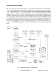
Figure 2-1 charts this dual-phase boot.
Figure 2-1 Dual-Phase Boot Flowchart
System Reset
Freescale Semiconductor, Inc...
Phase I: boot from on-board resources
Set OMR for boot from PCI and branch to bootstrap program
Phase II: boot from PCI (application code)
Run Application
2.2.1 Phase I: Boot From On-Board Resources
The Phase I boot is performed from on-board 24- or 8-byte wide memory or SCI, according to the
several operation modes present in the processor. The DSP hardware automatically starts executing the
bootstrap program according to the configuration of the MODA-D pins. Example 2-1 shows Phase I
boot code:
Example 2-1
INCLUDE "ioequ.asm"
INCLUDE "intequ.asm"
Phase I Boot Code
; X-Memory Mapped I/O Equates
; Interrupt Equates
PLL_INIT
EQU
$750012
;
;
;
;
PLL Initialization Word - 78.4 MHZ for a 33MHz
external crystal
PCI mode configuration MOD[D-A]=[1100]
Starting address of bootstrap code
PCI_OP_MODE
BOOT_START
EQU
EQU
$00000C
$ff0000
SIDR
SIVR
EQU
EQU
<system-dependent-value>; SIDR Value
<system-dependent-value>; SIVR Value
; PLL programming
movep
#PLL_INIT,x:M_PCTL
; HI32 Self-Configuration : Subsystem ID and Subsystem Vendor ID
move
#0,x0
; set constant
movep
#>$500000,x:M_DCTR
; Set Self Configuration Mode
rep #4
2-2
HI32 as a PCI Agent
For More Information On This Product,
Go to: www.freescale.com
Freescale Semiconductor, Inc.
Basics of HI32 PCI Usage
movep
x0,x:M_DPAR
movep
#SIDR,x:M_DPMC
movep
#SVID,x:M_DPAR
movep
x0,x:M_DCTR
jset
#M_ACT,x:M_DSR,*
; Transition to the Phase II Boot
move
omr,a
and
#$FFFFF0,a
or
#PCI_OP_MODE,a
move
a,omr
jmp
BOOT_START
;
;
;
;
;
set register pointer to SIDR/SVID
set SIDR value
set SVID value and write SIDR/SVID
personal software reset
wait for HACT = 0
; set PCI mode
; go to the bootstrap code start
Freescale Semiconductor, Inc...
As this example shows, the Phase I boot comprises the following steps:
1. Program the DSP internal PLL to achieve the minimum required DSP frequency for safe
HI32-PCI operation.
2. Program the HI32 configuration space while the HI32 is in Self-Configuration mode.1 In this step,
the Subsystem ID and Subsystem Vendor ID registers are programmed in case the system requires
them. In a self-configured system, other configuration space registers can also be programmed,
completing the self-configuration process. In a system with an external PCI configurator, any
other configuration space register programmed while the HI32 is in Self-Configuration mode may
be overwritten by the external configurator. The first four values written to HI32 configuration
space are irrelevant to the external configurator, which overwrites those values during its
configuration procedure.
3. Transition correctly to the Phase II boot from the host PCI bus through the HI32. This includes
changing the Chip Operation mode bits in the OMR Register to the corresponding value and
branching to the bootstrap program for the Phase II boot.
2.2.2 Phase II: Application Code Download From the PCI Bus
The second phase of the proposed dual-phase boot is a second run of the chipÕs bootstrap program, this
time in Host Bootstrap PCI Chip Operation mode. In this mode, the HI32 operates as a PCI target
(slave) with a 32-bit data transfer format.The bootstrap program reads one 32-bit word for the number
of program words to be downloaded, followed by another 32-bit word with the address of the location
to which the program should be downloaded, and then as many 32-bit words as are specified in the
first word received. Each 32-bit downloaded word contains a 24-bit DSP word in its three Least
Significant Bytes. The Most Significant Byte of the 32-bit word is ignored. At the end of the
downloading, the program runs, starting from the specified address.
The host can stop the downloading by setting the Host Flag 0. In this case, the downloaded code
executes from the starting address already specified. Section 3.9.2 addresses host flag usage.
Note:
For details on bootstrap modes and procedures, refer to the DSP userÕs manual for your
device.
1. See Section 2.4.1 for a broader explanation of Self-ConÞguration mode.
For More Information On This Product,
Go to: www.freescale.com
Freescale Semiconductor, Inc.
Basics of HI32 PCI Usage
2.3 PCI File Format
Freescale Semiconductor, Inc...
When using the sample drive/application provided in Appendix A, the program code to be
downloaded must be stored in an ASCII-data file with the following format:
¥
Each line contains a single 32-bit word in hexadecimal base.
¥
The 24-bit DSP word is right-aligned, zero extended, and mapped to a 32-bit word.
¥
The first line contains the number of program words in the program code (i.e. the number of
lines in the file minus two).
¥
The second line contains the destination DSP address of the code to be downloaded, which is
also the starting address at which execution begins after the bootstrap program executes.
¥
Every subsequent line contains only one program word, corresponding to a one 24-bit
hexadecimal program word for the DSP56301.
The HI32.PCI file provided with this application note presents this format.
2.4 PCI Configuration
HI32 configuration as a PCI agent requires programming of the HI32 Configuration Space registers.
This is achieved either by the HI32 Self-Configuration procedure or by an external configurator or by
a combination of both.
2.4.1 Self-Configured Systems
The HI32 Self-Configuration mode enables the interface to be configured as a PCI agent in systems
without an external configurator. It also enables the setting of some system-related PCI Configuration
Space fields (e.g., Subsystem ID) that may be needed by some systems, regardless of whether there is
an external configurator. Example 2-2 shows sample code that performs HI32 self-configuration.
Example 2-2
Self-Configuration Sample Code
INCLUDE "ioequ.asm"
INCLUDE "intequ.asm"
movep
#>$500000,x:M_DCTR
move
#$0,x0
movep
#CCMR_DATA,x:M_DPAR
movep
x0,x:M_DPAR
movep
#CLAT_DATA,x:M_DPAR
movep
#CBMA_DATA,x:M_DPAR
movep
#SIDR_DATA,x:M_DPMC
movep
#SVID_DATA,x:M_DPAR
movep
x0,x:M_DCTR
jset
#M_ACT,x:M_DSR,*
2-4
;
;
;
;
;
;
;
;
;
;
;
;
X-Memory Mapped I/O Equates
Interrupt Equates
HM=5 :
Self Configuration
write
dummy
write
write
to CCMR
write to (CCCR+CRID)
to CLAT
to CBMA
write to CSID
personal software reset
wait for HACT = 0
HI32 as a PCI Agent
For More Information On This Product,
Go to: www.freescale.com
Freescale Semiconductor, Inc.
Basics of HI32 PCI Usage
Note that writes to HI32 Configuration Space registers in Self-Configuration mode occur sequentially.
That is, all the configuration space registers in the sequence must be written, and none can be skipped.
Table 2.1 shows this sequence. Each write to DPAR accesses a register.
Table 2.1 Self-Configuration Mode Sequence
Freescale Semiconductor, Inc...
Sequential DPAR Write
Register
1
CSTR/CCMR
3
CHTY/CLAT
4
CBMA
5
CSID
2.4.2 Externally-Configured Systems
When PCI mode is set (HM = $1 in DCTR), an external configurator (e.g., a host computer) can
configure the HI32 as a PCI agent. During configuration, the host examines HI32 Configuration Space
registers for resource requirements and writes the HI32 configuration space with the corresponding
assigned resources and additional configuration settings.
We recommend that you do not directly change the configuration settings using the HI32 Self
Configuration mode (Section 2.4.1) unless it is guaranteed that the host can handle the new settings.
The host itself can safely make such changes during an interaction between the host configuration
software and the device driver.
The self-configuration procedure can be used to program Subsystem ID and Subsystem Vendor ID
prior to or concurrently with configuration space accesses by an external configurator. While the HI32
is not in PCI mode, any PCI access is retried by the HI32.
2.5 Reset Issues
Following are some considerations on host and DSP reset events:
¥
The HI32 reset (HRST pin) is decoupled from the DSP general reset (RESET pin). The
functionality of each of these pins is as follows:
Ñ HRST: Immediately floats PCI pins, resets the PCI state machines, and resets all
configuration space registers. It does not affect the data paths.
¥
¥
Ñ RESET: Completes the current PCI transaction, switches to HI32 mode 0, clears all the
FIFOs, and resets all DSP-side and host-side memory space status bits. It does not affect
PCI state machines or the configuration space registers.
The data status is reset only by a DSP general reset in order to maintain consistency of the data
status both on the DSP side and on the host side. Since all the FIFOs are cleared by this reset,
a DSP-host handshake should be accomplished to guarantee that data is not lost (if the
application requires it).
The host-side reset (HRST) does not reset the data status bits because a host-side reset does
not necessarily require a DSP-side reset. Therefore, the data in the FIFO should not be deleted.
If the data in the FIFOs must be cleared by a host-side reset, this reset should be achieved by
interaction between the host and the DSP applications (e.g., via the host commands
mechanism).
For More Information On This Product,
Go to: www.freescale.com
Freescale Semiconductor, Inc.
Freescale Semiconductor, Inc...
Basics of HI32 PCI Usage
2-6
HI32 as a PCI Agent
For More Information On This Product,
Go to: www.freescale.com
Freescale Semiconductor, Inc.
Data and Control Flow
3
Data and Control Flow
Freescale Semiconductor, Inc...
All data transfers through the HI32 are performed via three data FIFOs:
¥
Master DSP-to-host data FIFO (DSP Master Transmit/Host Master Receive Data FIFO
DTXM/HRXM), for DSP master operation.
¥
Slave DSP-to-host data FIFO (DSP Slave Transmit/Host Slave Receive Data FIFO
DTXS/HRXS), for DSP slave operation.
¥
Host-to-DSP data FIFO (DSP Receive/Host Transmit Data FIFO DRXR/HTXR) for both
master and slave operation.
Data synchronization between the DSP and host sides of the HI32 (data handshake) is achieved by
status bit polling, specific interrupts, or DMA requests. The relevant status bits that are polled on the
DSP side to synchronize data between the DSP and host sides of the HI32 are enumerated here:
¥
Slave operation:
¥
Ñ PCI Slave Transmit Data Request (STRQ) bit: indicates (when set to 1) that the DSP
Slave Transmit Data FIFO (DTXS) is not full and can be written.
Ñ PCI Slave Receive Data Request (SRRQ) bit: indicates (when set to 1) that the DSP
Receive Data FIFO (DRXR) is not empty and slave data can be read.
Master operation:
Ñ PCI Master Transmit Data Request (MTRQ) bit: indicates (when set to 1) that the DSP
Master Transmit Data FIFO (DTXM) is not full and can be written.
Ñ PCI Master Receive Data Request (MRRQ) bit: indicates (when set to 1) that the DSP
Receive Data FIFO (DRXR) is not empty and master data can be read).
3.1 DSP Side: Status Bits Polling Examples
In Example 3-1, both the SRRQ and STRQ bits in the DSR register are polled, and corresponding
duplex slave data transfers occur between the DSP56300 core and the DRXR and DTXS data FIFOs.
Note:
When data is written to a peripheral device, there is a two-cycle pipeline delay until any status
bits affected by this operation are updated. See the DSP56300 Family Manual for details on a
deviceÕs pipeline restrictions.
Example 3-1 Duplex Slave Data Transfers With Polling
READ_
WRITE_
brclr
movep
brclr
movep
#M_SRRQ,x:M_DSR,WRITE_
x:M_DRXR,x:(r0)+
#M_STRQ,x:M_DSR,READ_
y:(r1)+,x:M_DTXS
; Read data from FIFO
; Write data to FIFO
In Example 3-2, the MRRQ bit in the DPSR register is polled, and master data reads by the DSP56300
core occur from the DRXR FIFO.
Example 3-2 Master Data Receive With Polling
READ_
do
brclr
movep
#N,END_
#M_MRRQ,x:M_DPSR,READ_
x:M_DRXR,x:(r0)+
; Read N words
; Read data from FIFO
END_
For More Information On This Product,
Go to: www.freescale.com
Freescale Semiconductor, Inc.
Data and Control Flow
In Example 3-3, the MTRQ bit in the DPSR register is polled, and master data writes by the 56300
core occur to the DTXM FIFO.
Example 3-3 Master Data Transmit With Polling
do
brclr
movep
nop
nop
WRITE_
#N,END_
#M_MTRQ,x:M_DSR,WRITE_
y:(r1)+,x:M_DTXM
; Write N words
; Write data to FIFO
; NOPs are placed due to
; a two cycle pipeline delay
END_
Freescale Semiconductor, Inc...
The NOP instructions in this last example are inserted because of pipeline restrictions and can be
replaced by any other useful instructions.
In Example 3-4, both the SRRQ bit in the DSR register and the MRRQ bit in the DPSR register are
polled, and corresponding mixed master/slave data reads by the DSP56300 core occur from the DRXR
data FIFO.
Example 3-4 Mixed Master/Slave Data Transfers With Polling
SREAD_
brclr
movep
brclr
movep
MREAD_
#M_SRRQ,x:M_DSR,MREAD_
x:M_DRXR,x:(r0)+
#M_MRRQ,x:M_DSR,SREAD_
x:M_DRXR,y:(r1)+
; Read slave data
; Read master data
If the DTXS or DTXM data FIFO is empty (for example, after the personal software reset), then the
corresponding FIFO can be filled without STRQ or MTRQ status bit polling.
3.2 Host-Side Transfers: Status Polling
Three status bits in the HSTR register reflect the status of the HTXR and HRXS FIFOs:
Note:
¥
PCI Host Transmitter Ready (TRDY) bit: indicates (when set to 1) that the Host Transmit
Data FIFO (HTXR) is empty and can accept writes from the host.
¥
PCI Host Transmit Data Request (HTRQ) bit: indicates (when set to 1) that the Host Transmit
Data FIFO (HTXR) is not full and can accept writes from the host.
¥
PCI Host Receive Data Request (HRRQ) bit: indicates (when set to 1) that the Host Slave
Receive Data FIFO (HRXS) is not empty and can be read by the host.
These bits address HI32 slave data only.
In the PCI mode, these bits should not necessarily be polled. If the corresponding FIFO is not ready,
the HI32 hardware inserts wait states.
3.2.1 Host Side: Status Bit Polling Examples
The pseudo code examples in this section illustrate polling of the host-side status bit. Example 3-5
shows HTRQ polling for HI32 slave host-to-DSP data transfers, and Example 3-6 shows HRRQ
polling for HI32 slave DSP-to-host data transfers.
Example 3-5 HTRQ Polling (Pseudo Code)
Wait_For_HTRQ_Set
Write_HTXR
3-2
; FIFO is not full
; send Data
HI32 as a PCI Agent
For More Information On This Product,
Go to: www.freescale.com
Freescale Semiconductor, Inc.
Data and Control Flow
Example 3-6 HRRQ Polling (pseudo code)
Wait_For_HRRQ_Set
Write_HRXS
; FIFO is not empty
; read Data
Freescale Semiconductor, Inc...
The TRDY bit has two additional applications:
¥
If TRDY is set to one, the data written from the host processor to the HTXR is immediately
transferred to the DSP side of the HI32. This has many applications. For example, if the host
processor issues a host command that causes the DSP56300 core to read the DRXR, the host
processor is guaranteed that the data it transfers to the HI32 is received by the DSP56300 core
(see Example 3-7).
¥
High-speed data transfers (no wait states): if TRDY is set in PCI data transfers with HTF≠$0
(i.e., not in 32-bit mode), the HI32 does not insert wait states into the next six data transfers
written by the host to the HTXR. If TRDY is set in PCI data transfers with HTF=$0 (i.e.,
32-bit mode), the HI32 does not insert wait states into the next three data phases written by the
host to the HTXR.
Example 3-7 TRDY Polling: Host Command
Host Side (pseudo code):
Wait_For_TRDY_Set
Write_HTXR
Write_HCVR_With_HC_Set
; guarantees that DRXR is empty
; send Message
; send Host Command
DSP Side (Host Command Interrupt Service Routine):
HC_ISR
movep
jsr
x:M_DRXR,x0
<#LONG_ISR
;
;
;
;
read Message
SRRQ polling is not necessary
because protocol guarantees data
integrity
3.3 32-Bit and Non-32-Bit Mode Support
The DSP-side status bits should be tested for each transferred word (non-32-bit mode) or part of word
(32-bit mode).
3.4 DMA Usage
The DMA Request Source bits in the DMA Control registers (DRS4-DRS0) encode the source of
DMA requests that trigger the DMA transfers. For example, Table 3-1 shows the HI32-related DMA
request source encoding for the DSP56301. The DMA controller can transfer data to/from the HI32 at
a maximum rate of one word every two internal DSP clock cycles. To guarantee proper operation,
DMA should service the HI32 under the following restrictions:
¥
DMA should not service the DRXR FIFO in master/slave mixed mode because the master or
slave data may be fetched by the DMA channel(s) in the wrong order.
¥
The DMA data transfers should not be concurrent with the DSP56300 core data transfers
to/from the same HI32 data FIFO.
The DMA Transfer mode should be set to word transfer triggered by request because the DMA
controller should access the HI32 data register only when it is readyÑi.e., according to the
corresponding DMA request.
For More Information On This Product,
Go to: www.freescale.com
Freescale Semiconductor, Inc.
Data and Control Flow
Table 3-1HI32-Related DMA Request Source Encoding (for the DSP56301)
DMA Request Source Bits DRS4...DRS0
Requesting Device
11100
HI32 Slave Receive Data
11101
HI32 Master Receive Data
11110
HI32 Slave Transmit Data
11111
HI32 Master Transmit Data
3.4.1 Slave Operation
Freescale Semiconductor, Inc...
The slave transmit data DMA request is generated under the following conditions:
¥
The DMA channel is programmed to handle slave transmit data.
¥
The HI32 is in PCI mode.
¥
The DTXS is not full.
The slave receive data DMA request is generated under the following conditions:
¥
The DMA channel is programmed to handle slave receive data.
¥
The HI32 is in PCI mode.
¥
The DRXR contains slave data.
Example 3-8 shows DMA initialization for non 32-bit slave transmit data transfers.
Example 3-8 DMA Initialization: Slave Transmit (Non 32-Bit)
;
;
;
;
;
;
;
;
;
;
;
;
movep
#>Slave_Tx_ptr,x:M_DSR0
movep
#>M_DTXS,x:M_DDR0
movep
#>Word_Num,x:M_DCO0
movep
#>$8ef250,x:M_DCR0
DCR0 Bits:
DE=1: DMA enabled
DIE=0: DMA interrupt disabled;
DTM[2:0]=001: Triggered by request, word transfer
DPR[1:0]=11: Priority Level 3 (highest)
DCON=0: continuous mode disabled
DRS[4:0]=11110: HI32 Slave Transmit Data
D3D=0: three dimensional mode disabled
DAM[5:3]=100: destination address - no update
DAM[2:0]=101: source address - post-increment by 1
DDS[1:0]=00: destination memory space - X
DSS[1:0]=00: source memory space - X
; Word_Num = PCI_Word_Num - 1
Example 3-9 shows DMA initialization for 32-bit slave receive data transfers. Here the number of
words transferred by the DMA is twice the number of words transferred by the HI32 as a PCI master.
All 16-bit words (half words of the 32-bit words) are saved in DSP memory in the big-endian order as
shown in Table 3-2. (Slave_Rx_ptr should point to Address+1). Note that this organization is
achieved via DMA three-dimensional addressing mode. The usage of DMA linear addressing results
in data organized in DSP memory in little-endian order. Consult Appendix B for references on DMA
usage.
3-4
HI32 as a PCI Agent
For More Information On This Product,
Go to: www.freescale.com
Freescale Semiconductor, Inc.
Data and Control Flow
Freescale Semiconductor, Inc...
Example 3-9 DMA Initialization: Slave Receive (32-Bit, Big Endian Order)
;
;
;
;
;
;
;
;
;
;
;
;
movep
#>Slave_Rx_ptr,x:M_DDR0
movep
#>M_DRXR,x:M_DSR0
movep
#>(Word_Num<<12),x:M_DCO0
; Word_Num = (2 * PCI_Word_Num) + 1
movep
#-1,x:M_DOR2
movep
#3,x:M_DOR3
movep
#>$8ee640,x:M_DCR0
DCR0 Bits:
DE=1: DMA enabled
DIE=0: DMA interrupt disabled;
DTM[2:0]=001: Triggered by request, word transfer
DPR[1:0]=11: Priority Level 3 (highest)
DCON=0: continuous mode disabled
DRS[4:0]=11100: HI32 Slave Receive Data
D3D=1: three dimensional mode enabled
DAM[5:3]=100: source address - no update
DAM[2:0]=100: dest.address - three-dimensional (DOR2/3)
DDS[1:0]=00: destination memory space - X
DSS[1:0]=00: source memory space - X
Table 3-232-Bit Data Big Endian Order
Memory
Address
DMA
Transfer
Order
DSP Data
PCI Data
Address
Address+1
Address+2
Address+3
2
1
4
3
word1[31:16]
word1[15:0]
word2[31:16]
word2[15:0]
...
...
...
...
word1[31:0]
word2[31:0]
3.4.2 Master Operation
The master transmit data DMA request is generated under the following conditions:
¥
The DMA channel is programmed to handle master transmit data.
¥
The HI32 is in PCI mode.
¥
DTXM is not full.
The master receive data DMA request is generated under the following conditions:
¥
The DMA channel is programmed to handle master receive data.
¥
The HI32 is in PCI mode.
¥
DRXR contains master data.
Example 3-10 shows DMA initialization for 32-bit master transmit data transfers. Here the number of
words transferred by the DMA is twice the number of words transferred by the HI32 as a PCI master.
All 16-bit words (half words of the 32-bit words) are saved in the DSP memory in the little endian
order as shown in Table 3-3 (Master_Tx_ptr should point to Address).
For More Information On This Product,
Go to: www.freescale.com
Freescale Semiconductor, Inc.
Data and Control Flow
Freescale Semiconductor, Inc...
Example 3-10 DMA Initialization: Master Transmit (32-Bit, Little Endian Order)
;
;
;
;
;
;
;
;
;
;
;
;
movep
#>Master_Tx_ptr,x:M_DSR0
movep
#>M_DTXM,x:M_DDR0
movep
#>Word_Num,x:M_DCO0
movep
#>$8efa50,x:M_DCR0
DCR0 Bits:
DE=1: DMA enabled
DIE=0: DMA interrupt disabled;
DTM[2:0]=001: Triggered by request, word transfer
DPR[1:0]=11: Priority Level 3 (highest)
DCON=0: continuous mode disabled
DRS[4:0]=11111: HI32 Master Transmit Data
D3D=0: three dimensional mode disabled
DAM[5:3]=100: destination address - no update
DAM[2:0]=101: source address - post-increment by 1
DDS[1:0]=00: destination memory space - X
DSS[1:0]=00: source memory space - X
; Word_Num = (2 * PCI_Word_Num) + 1
Table 3-332-Bit Data Little Endian Order
Memory
Address
Address
Address+2
Address+3
1
2
3
4
word1[15:0]
word1[31:16]
word2[15:0]
word2[31:16]
DMA
Transfer
Order
DSP Data
Address+1
...
...
...
PCI Data
...
word1[31:0]
word2[31:0]
3.4.3 32-Bit And Non-32-Bit Mode Support
For 32-bit mode data transfer, two consecutive DMA requests per one PCI word are generated: first for
two least significant bytes of the 32-bit word and then for the two most significant bytes. The
corresponding DMA channel can be programmed to transfer parts of the 32-bit word in Ôlittle endianÕ
or Ôbig endianÕ order (see Example 3-9). For a non-32-bit mode data transfer, one DMA request per
PCI word is generated.
3.5 Interrupts
To simplify data handling, the HI32 supplies four separate interrupt service requests: Master Receive,
Master Transmit, Slave Receive and Slave Transmit. Data transfer interrupts can be either short or
long. A long interrupt executes if one of the interrupt instructions fetched is a JSR-type instruction. If
more than one interrupt request is pending when an instruction executes, the interrupt source with the
highest interrupt priority level (IPL) is serviced first. When multiple interrupt requests with the same
IPL are pending, a second fixed-priority structure within that IPL determines which interrupt source is
serviced. The fixed priority of interrupts sources within an IPL is shown in the userÕs manual for each
DSP56300 family device.
3-6
HI32 as a PCI Agent
For More Information On This Product,
Go to: www.freescale.com
Freescale Semiconductor, Inc.
Data and Control Flow
Any interrupt request can be disabled during the long interrupt in one of two ways:
¥
Clearing the corresponding interrupt enable bit in the DCTR or DPCR register
¥
Masking the interrupt in the SR register
To prevent an additional interrupt request, it should be disabled before the actual interrupt service (i.e.,
before the corresponding data register access).
Section 3.5.1 and Section 3.5.2 elaborate on the generation conditions of HI32 data transfer interrupt
requests.
3.5.1 Slave Operation
Freescale Semiconductor, Inc...
The slave transmit data interrupt request is generated under the following conditions:
¥
The HI32 is in PCI mode.
¥
The STRQ status bit is set in the DSR.
¥
The Slave Transmit Interrupt Enable (STIE) bit is set in the DCTR.
¥
The HI32 Interrupt Priority Level (HPL1-HPL0 in IPRP) is higher than the interrupt masking
level defined by bits I1-I0 in the SR.
The slave receive data interrupt request is generated under the following conditions:
¥
The HI32 is in PCI mode.
¥
The SRRQ status bit is set in the DSR.
¥
The Slave Receive Interrupt Enable (SRIE) bit is set in the DCTR.
¥
The HI32 Interrupt Priority Level (HPL1-HPL0 in IPRP) is higher than the interrupt masking
level defined by bits I1-I0 in the SR.
Example 3-11 shows how slave transmit and receive data transfer interrupts are handled.
Example 3-11 Slave Data Transfers Interrupt Handling
; HI32 Slave Receive Data short interrupt
org
p:I_HSR
movep
x:M_DRXR,x:(r0)+
nop
; Read data from FIFO
; HI32 Slave Transmit Data short interrupt
org
p:I_HST
movep
y:(r1)+,x:M_DTXS
; Write data to FIFO
nop
...
; Set interrupt priority and masking levels (initialization part of the code)
move
#$0,sr
; I1-I0 = $0
movep
#$3,x:M_IPRP
; HPL1-HPL0=$3
...
3.5.2 Master Operation
The master transmit data interrupt request is generated under the following conditions:
¥
The HI32 is in PCI mode.
¥
The MTRQ status bit is set in the DPSR.
For More Information On This Product,
Go to: www.freescale.com
Freescale Semiconductor, Inc.
Data and Control Flow
¥
The Master Transmit Interrupt Enable (MTIE) bit is set in the DPCR.
¥
The HI32 Interrupt Priority Level (HPL1-HPL0 in IPRP) is higher than the interrupt masking
level defined by bits I1-I0 in the SR.
Freescale Semiconductor, Inc...
The master receive data interrupt request is generated under the following conditions:
¥
The HI32 is in PCI mode.
¥
MRRQ status bit is set in the DPSR.
¥
The Master Receive Interrupt Enable (MRIE) bit is set in the DPCR.
¥
The HI32 Interrupt Priority Level (HPL1-HPL0 in IPRP) is higher than the interrupt masking
level defined by bits I1-I0 in SR.
Example 3-12 shows how master transmit data transfer long interrupts are handled. Here the interrupt
service is disabled after N data transfers.
Example 3-12 Master Data Transfers Interrupt Handling
; HI32 Master Transmit Data long interrupt (initialization part of the code)
org
p:I_HPMT
jsr
MTI_
; call interrupt service
nop
...
; Set interrupt priority and masking levels
move
#$0,sr
movep
#$3,x:M_IPRP
...
; HI32 Master Transmit Data long interrupt
; (stop interrupt generation after N transfers)
MTI_
move
r1,a
cmp
#N,a
jlt
READ_
bclr
#M_MTIE,x:M_DPCR
READ_
movep
y:(r1)+,x:M_DTXM
; I1-I0 = $0
; HPL1-HPL0=$3
; clear interrupt enable
; Write data to FIFO
rti
3.5.3 32-Bit And Non-32-Bit Mode Support
For 32-bit mode data transfers, two separate interrupt requests are generated: first for the two least
significant bytes of the 32-bit word, and then for the two most significant bytes. For non-32-bit mode
data transfers, one interrupt per word is generated.
3.6 Data Handling
3.6.1
DSP-to-Host Data Path
The data path between the DSP and the Host is composed of two FIFOs:
3-8
¥
DSP Master Transmit/Host Master Receive Data FIFO (DTXM/HRXM), for DSP master
operation;
¥
DSP Slave Transmit/Host Slave Receive Data FIFO (DTXS/HRXS), for DSP slave operation.
HI32 as a PCI Agent
For More Information On This Product,
Go to: www.freescale.com
Freescale Semiconductor, Inc.
Data and Control Flow
Table 3-4 summarizes the configurations for this path.
Table 3-4DSP to Host Data Path Summary
Freescale Semiconductor, Inc...
HI32 Master/Slave
32-/24-bit wide
FIFO
FIFOÕs Depth
See Figure
MASTER
24: FC[1:0]π ≠ 0
DTXM/HRXM
8
Figure 3-1
MASTER
32: FC[1:0]
=0
DTXM/HRXM
4
Figure 3-2
SLAVE
24: HRF
≠0
DTXS/HRXS
6
Figure 3-3
SLAVE
32: HRF
=0
DTXS/HRXS
3
Figure 3-4
Figure 3-1 DSP-To-Host Data Path (Master, 24-Bit Wide)
DSP DMA Bus
DSP Global Data Bus
24
24
DTXM
HRXM
24
data transfer command converter
(FC[1:0]π ≠ 0)
32
Host Bus
For More Information On This Product,
Go to: www.freescale.com
Freescale Semiconductor, Inc.
Data and Control Flow
Figure 3-2
DSP-To-Host Data Path (Master, 32-Bit Wide)
DSP DMA Bus
DSP Global Data Bus
24
24
DTXM
Freescale Semiconductor, Inc...
x
x
x
x
x
x
x
x
HRXM
32
data transfer command converter
(FC[1:0] = 0)
32
Host Bus
Figure 3-3
DSP-To-Host Data Path (Slave, 24-Bit Wide)
DSP DMA Bus
DSP Global Data Bus
24
24
DTXS
HRXS
24
data transfer command converter
(HRF[1:0] ≠ 0)
32
Host Bus
3-10
HI32 as a PCI Agent
For More Information On This Product,
Go to: www.freescale.com
Freescale Semiconductor, Inc.
Data and Control Flow
Figure 3-4 DSP-To-Host Data Path (Slave, 32-Bit Wide)
DSP DMA Bus
DSP Global Data Bus
24
24
DTXS
Freescale Semiconductor, Inc...
x
x
x
x
x
x
HRXS
32
data transfer command converter
(HRF[1:0] = 0)
32
Host Bus
HRXS and HRXM accesses are extended as follows:
¥
If the HI32 is the PCI target in a read transaction from the HRXS while it is empty and the
TWSD bit in the HCTR register is cleared, the HI32 inserts PCI wait states to extend the
current data phase until the data is transferred from the DSP side to the HRXS. Up to eight
wait states can be inserted before a target-initiated transaction termination (disconnect or
retry) is generated.
¥
If the HI32 is the target in a read transaction from the HRXS while it is empty and the TWSD
bit in HCTR register is set, the HI32 generates a target-initiated transaction termination
(disconnect or retry).
¥
If the HI32 is the active PCI master in a write transaction and the MWSD bit in the DPCR is
cleared, it inserts wait states to extend the current data phase if it cannot guarantee the
completion of the next data phase. The HI32 asserts the HIRDY pin and completes the current
data phase under one of the following circumstances:
¥
Note:
Ñ It can complete the next data phase (HRXM is not empty).
Ñ It has determined to terminate the transaction due to time-out, master abort, or target
disconnect.
Ñ It has determined to terminate the transaction due to burst completion.
If the HI32 is the active PCI master in a write transaction and the MWSD bit in the DPCR is
set, the HI32 does not insert wait states. If it cannot guarantee the completion of the next data
phase (HRXM is empty), the HI32 completes the current data phase and terminates the
transaction.
The HI32 does not initiate the transaction as a PCI master if it cannot guarantee the
completion of at least one data phase.
For More Information On This Product,
Go to: www.freescale.com
Freescale Semiconductor, Inc.
Data and Control Flow
The HI32 has separate master and slave DSP-to-host FIFOs for data retention, as illustrated in the
following scenario:
¥
The HI32 transmits to the host as a master, using DTXM/HRXM.
¥
The HI32 is interrupted by another master and temporarily becomes a slave, responding to the
new master using DTXS/HRXS.
¥
After the response is complete, the HI32 resumes the original transmission as a master, using
DTXM/HRXM. Any data previously inserted into this FIFO remains intact during the slave
transmission, so the HI32 can resume as a master from exactly where it stopped.
Freescale Semiconductor, Inc...
3.6.2 Host-to-DSP Data Path
The data path between the host and the DSP is implemented by the DSP Receive/Host Transmit Data
FIFO (DRXR/HTXR) for both master and slave operation. Table 3-5 summarizes the configuration
possibilities for this path.
Table 3-5Host-to-DSP Data Path Summary
HI32 Master/Slave
32-/24-bit wide
FIFO
FIFOÕs Depth
See Figure
MASTER
24: FC[1:0]
≠0
DRXR/HTXR
6
Figure 3-5
MASTER
32: FC[1:0]
=0
DRXR/HTXR
3
Figure 3-6
SLAVE
24: HTF
≠0
DTXS/HRXS
6
Figure 3-5
SLAVE
32: HTF
=0
DRXR/HTXR
3
Figure 3-6
Figure 3-5
Host-To-DSP Data Path (24-Bit Wide)
DSP DMA Bus
DSP Global Data Bus
24
24
DRXR
HTXR
24
data transfer command converter
(HTF[1:0] ≠ 0)
(FC[1:0] ≠ 0)
32
Host Bus
3-12
HI32 as a PCI Agent
For More Information On This Product,
Go to: www.freescale.com
Freescale Semiconductor, Inc.
Data and Control Flow
Figure 3-6 Host-To-DSP Data Path (32-Bit Wide)
DSP DMA Bus
DSP Global Data Bus
24
24
DRXR
Freescale Semiconductor, Inc...
0
0
0
0
0
0
HTXR
32
data transfer command converter
(HTF[1:0] = 0)
(FC[1:0] = 0)
32
Host Bus
HTXR accesses are extended as follows:
¥
If the HI32 is the PCI target in a write transaction to the HTXR while it is full and the TWSD
bit in the HCTR register is cleared, the HI32 inserts PCI wait states to extend the current data
phase. Wait states are inserted until the data is transferred from the HTXR to the DSP side. Up
to eight wait states can be inserted before a target-initiated transaction termination (disconnect
or retry) is generated.
¥
If the HI32 is the target in a write transaction to the HTXR while it is full and the TWSD bit in
the HCTR register is set, the HI32 generates a target-initiated transaction termination
(disconnect or retry).
¥
If the HI32 is the active PCI master in a read transaction and the MWSD bit in the DPCR
register is cleared, the HI32 inserts wait states to extend the current data phase if it cannot
guarantee the completion of the next data phase. The HI32 asserts the HIRDY pin and
completes the current data phase under one of the following circumstances:
¥
Ñ It can complete the next data phase (HTXR is not full).
Ñ It has determined to terminate the transaction due to time-out, master abort, or target
disconnect.
Ñ It has determined to terminate the transaction due to burst completion.
If the HI32 is the active PCI master in a read transaction and the MWSD bit in the DPCR
register is set, the HI32 does not insert wait states. If it cannot guarantee the completion of the
next data phase (HTXR is full), the HI32 completes the current data phase and terminates the
transaction.
For More Information On This Product,
Go to: www.freescale.com
Freescale Semiconductor, Inc.
Data and Control Flow
Note:
The HI32 does not initiate the transaction as a PCI master if it cannot guarantee the
completion of at least one data phase.
The HI32 uses the same FIFO to transmit master and slave data on the Host-to-DSP data path.
Simultaneous slave and master data transfers on the host-to-DSP data path must use the same data
format (see Section 3.8). Unless the HI32 acts only as a master or only as a slave for data transfers via
the DRXR/HTXR FIFO, the application must manage data in the FIFO so that master and slave data
can be distinguished. It must also manage data in the FIFO so that data simultaneously transferred
from different external masters can be distinguished.
Freescale Semiconductor, Inc...
3.6.2.1
Management of Mixed Master/Slave Data
Mixed slave and master data in the DRXR/HTXR FIFO is handled through the synchronization
mechanism (polling, interrupt or DMA) chosen for control of the data flow. Two guidelines must be
followed to guarantee proper operation:
¥
Polling and interrupt techniques should be used in any combination for distinguishing master
and slave data.
¥
DMA should be used only for non-mixed data (slave-only or master-only) present in the
DRXR/HTXR FIFO.
One way to manage mixed master/slave data is to use host commands and host flags for inter-process
communication, as discussed in Section 3.9.5, "Example: Master/Slave Data Mixing Management."
3.6.2.2 Management of Mixed Multiple External Masters Data
This section describes the use of the Receive Buffer Lock Enable (RBLE) bit and the Host Data
Transfer Complete (HDTC) bit. These bits prevent mixing of data from different external PCI masters
in the DRXR/HTXR FIFO (see Table 3-6). The RBLE bit can guarantee only that the data from
different external masters is not mixed in the HTXR/DRXR FIFO. It cannot guarantee that the slave
data (written by an external master) and master data (read by the HI32 as master) are not mixed. The
master and slave data are separated by polling the MRRQ and SRRQ bits or by interrupts.
With RBLE set, the data transfer from the host to the DSP is not complete until the DRXR FIFO has
been emptied by DSP core reads from the DSP side.
Table 3-6 Managing Multiple Master Data in the DRXR/HTXR FIFO
Event
Status
A personal software reset of
the HI32 is performed
RBLE = 0
HDTC = 0
The core sets RBLE, then enters
PCI mode (HM = $1)
RBLE = 1
HDTC = 0
3-14
Description
•
With RBLE is set, the DRXR/HTXR FIFO is protected
from containing data from more than one external master
write burst at any time. In terms of external masters only,
the DRXR/HTXR FIFO is locked and exclusive write
transactions can now be made to it.
•
No data transfer has completed, so HDTC = 0.
HI32 as a PCI Agent
For More Information On This Product,
Go to: www.freescale.com
Freescale Semiconductor, Inc.
Data and Control Flow
Freescale Semiconductor, Inc...
Table 3-6 Managing Multiple Master Data in the DRXR/HTXR FIFO (Continued)
Event
Status
Description
An external PCI master performs a
write transaction into the
DRXR/HTXR FIFO. The burst
completes but data remains in the
FIFO (the DSP may have read
some of it from DRXR, but it has
not yet read all the data out of the
FIFO).
RBLE = 1
HDTC = 0
•
All the data of the transaction has not yet been read by
the DSP core, so HDTC is still zero.
•
The HI32 issues a target retry to any external master that
attempts to initiate a new burst to the DSP (whether or
not the same master sent the just-completed burst to the
DSP).
The core reads all remaining data
from the DRXR/HTXR FIFO.
RBLE = 1
HDTC = 1
•
All the data of the transaction has been read by the DSP
core, so HDTC = 1. Since the reads from DRXR can be
done by an interrupt handler or by DMA, some core
control code may not be notified when the DRXR/HTXR
FIFO empties. Therefore, HDTC = 1 alerts the core
control code of the empty status.
•
Since the core control code has not acknowledged the
receipt of this status, the HI32 continues to issue a target
retry to any external master, which attempts to initiate a
new burst to the HTXR.
•
The core acknowledges that the PCI transaction is fully
received and fully read out of the HTXR/DRXR FIFO.
Thus, a new transaction into the HTXR can be accepted
if an external master initiates it.
Core clears HDTC by writing it “1”.
RBLE = 1
HDTC = 0
3.7 PCI-to-DSP Address Mapping
While the HTXR FIFO occupies 16377 (16K - 7) words of the PCI memory space, all the memory
writes to HTXR are transferred to the DRXR register as an output stage of the HTXR/DRXR FIFO. It
is the userÕs responsibility to define where the DRXR data is to be sent.
Some applications require dynamic PCI-to-DSP address mapping as a function of a PCI transaction
start address used for an HTXR register write. This mapping can be done in different ways, for
example:
¥
Host commands: Host commands can be sent before an HTXR access, defining the address
where DRXR data is to be written (either by the core or DMA).
¥
Address insertion feature: The DSP can read the PCI transaction address used for host-to-DSP
writes (through the HTXR) if the address insertion feature is enabled. This feature is
controlled by the IAE bit in the DPCR register. The first word (2 words in the 32-bit mode)
placed in the host-to-DSP FIFO (HTXR/DRXR) is really the PCI address. Software can use
this datum to define where DRXR data should be written in DSP memory.
3.8 Data Format Conversion
Since the PCI bus is 32 bits wide but the DSP internal registers/buses are 24 bits wide, the format
(width and alignment) of the data transferred between the HI32 and another PCI agent is
programmable. Data width and alignment are programmed for master, slave, and each data path
independently through the following bits:
For More Information On This Product,
Go to: www.freescale.com
Freescale Semiconductor, Inc.
Data and Control Flow
¥
For master operation Ñ DSP Data Transfer Format Control (FC[1:0]) bits in the DSP PCI
Master Control (DPMC) Register
¥
For slave operation Ñ Host Transmit Data Transfer Format (HTF[1:0]) bits and the Host
Receive Data Transfer Format (HRF[1:0]) bits in the HI32 Control Register (HCTR)
For all available data format options, refer to the userÕs manual for your device.
Freescale Semiconductor, Inc...
3.8.1 Slave Data Format Control
To switch between 32-bit and non-32 bit HI32 slave data width/alignment, change the Host
Transmit/Receive Data Transfer Format (HTF[1:0],HRF[1:0]) bits in the HI32 Control Register
(HCTR) from the host side. This can be done only after the HI32 is in personal software reset (PSR)
state and before the first use of the corresponding FIFO. For each of the three data paths, the
HTXR/DRXR, DTXS/HRXS, DTXM/HRXM data format can be changed independently. Table 3-7
and Table 3-8 present two possible approaches to switching the HI32 slave between 32-bit and
non-32-bit modes on the fly.
Table 3-7HINTA Signaling
DSP
Host
The DSP core clears HI32 mode (HM) bits and waits
until the HACT bit is zero (personal software reset).
The DSP asserts HINTA by setting the HINT bit in
DCTR to notify host that the HI32 is in personal software
reset (PSR) state. Note that the HI32 initiates PSR by
clearing HM, but it is not actually in the PSR state until
HACT is zero.
The host receives the interrupt and switches HTF/HRF
to the desired mode.
The host sends any host command (e.g. HC#1).
An interrupt service routine resulting (ISR) from the host
command (HC#1) clears the HINT bit in the DCTR,
causing HINTA deassertion.
Table 3-8Host Flag / Host Command Handshaking
DSP
HOST
HF3, which is used as PSR status to host, is initially
clear. Note that HF[5:3] are written from the DSP side of
the HI32, and HF[2:0] are written from the host side.
The host clears HF0, thus notifying the core of
a slave data format change status, sends a host command (e.g. HC#2) to request Personal Software Reset
(PSR), and waits for HF3 -> 1.
3-16
HI32 as a PCI Agent
For More Information On This Product,
Go to: www.freescale.com
Freescale Semiconductor, Inc.
Data and Control Flow
Table 3-8Host Flag / Host Command Handshaking (Continued)
DSP
HOST
The DSP receives host command (HC#2). Then the ISR
resulting from the host command initiates PSR (clears
HM[2:0] and waits for HACT -> 0). The ISR sets HF3
and then waits for HF0 -> 1.
Host reads HF3 = 1, changes HTF/HRF to the desired
mode, and then sets HF0.
Freescale Semiconductor, Inc...
The DSP reads HF0 = 1, clears HF3, and exits the ISR.
3.8.2 Master Data Format Control
The HI32 master data width/alignment is controlled from the DSP side, using the Format Control bits
(DPMC(FC[1:0])). The 32-bit to non-32-bit modification of FC[1:0] is subject to the same restriction
as the HTF/HRF. However, since the DSP can change both the FC[1:0] and HM[1:0] bits,
inter-processor communication is not needed in this case.
Note:
If master and slave data are mixed in the host-to-DSP FIFO, data of the same width and
alignment should be used for master and slave transfers.
3.9 Control Flow
The use of host commands, host flags, slave data, semaphores, the HINTA signal, or any combination
of them enables a flexible implementation of control protocol between the host and the DSP. Table
3-7 demonstrates use of the HINTA signal. This section discusses other control flow considerations.
3.9.1 Host Commands
HI32 host commands are a powerful way to control the DSP through the PCI bus by enabling the user
to define up to 128 programmable interrupt service routines (ISRs), which are set up by the host upon
writing to the HCVR. A host command interrupt can be generated as a Non-Maskable Interrupt by
setting the Host Non-Maskable Interrupt (HNMI) bit in the HCVR. The interrupt is then processed
with the highest priority, regardless of the current HI32 interrupt priority and HCIE bit status in the
DCTR.
3.9.2 Host Flags
The HI32 host flags are general-purpose flags for DSP-host intercommunication:
¥
HF[2:0] for host-to-DSP signalling: written by the host in the HCTR and read by the DSP in
the DSR
¥
HF[5:3] for DSP-to-host signalling: written by the DSP in the DCTR and read by the host in
the HSTR
For More Information On This Product,
Go to: www.freescale.com
Freescale Semiconductor, Inc.
Data and Control Flow
Figure 3-7 illustrates the use of host flags.
Figure 3-7
Host Flags Usage
DSP writes
DSP reads
DCTR
HF5
HF4
DSR
HF3
HF2
HSTR
HF0
HCTR
Host reads
Freescale Semiconductor, Inc...
HF1
Host writes
3.9.3 Slave Data
By polling the TRDY bit in the HSTR, the host can synchronize host commands with HI32 slave data
to be handled by the corresponding ISR. Refer to Section 3.2 for TRDY usage.
3.9.4 Semaphores
One common use of semaphores is to ensure unique access to the HI32 by an external master. With the
HI32 in PCI mode, unique access is achieved by an external master using the HLOCK signal to
perform a bus lock (locking the entire PCI bus) or a resource lock (locking a given PCI target or a
portion of its memory). The latter method is preferred because it allows more efficient use of the bus.
Locking is a two-tier process. The HLOCK signal updates the semaphore without interference. Then
the new semaphore value guarantees the current owner exclusive access to the protected resource. The
coding of the semaphore is implementation-dependent. A zero value in the semaphore can indicate that
the shared resource (in this case, the HI32) is available. In the remainder of this discussion, it is
assumed that this method is used. Locking works as follows:
3-18
¥
Setting the semaphore: A master is granted the bus and, noting that HLOCK is not asserted,
can assert HLOCK to lock the bus or resource. This is done in the transaction the master uses to
read the semaphore to prevent another master from changing the semaphore before this master
can write an update to the semaphore. During each transaction it makes as the lock owner, the
locking master must actually deassert HLOCK during the address phase and assert it during the
data phase(s). If HLOCK is asserted during an entire burst to a locked target (or any target, if
the entire bus is locked), the target notices that the initiator is not the locking master and issues
a retry to this initiator. The locking master (or operating system task within a master) writes its
signature code into the semaphore if the semaphore is currently zero. At the end of the burst,
this master unlocks the bus by deasserting HLOCK. If the semaphore is already non-zero, the
locking master must try the semaphore again later and re-check for zero.
¥
Accessing resource: If the locking master becomes the new semaphore owner, it can now
exclusively access the semaphore-protected resource.
¥
Releasing the resource: When the semaphore owner finishes using the protected resource, it
must clear the semaphore in the same way that it set it, except that the semaphore is cleared
instead of written with a signature value.
HI32 as a PCI Agent
For More Information On This Product,
Go to: www.freescale.com
Freescale Semiconductor, Inc.
Data and Control Flow
3.9.5 Example: Master/Slave Data Mixing Management
Example 3-13 shows how to solve the master/slave data mixing problem using a combination of host
commands and host flags. In this example, the following definitions apply:
¥
Host Command 1 (HC1) - host requests HTXR
¥
Host Command 2 (HC2) - host clears HF3
¥
Host Command 3 (HC3) - host releases HTXR
¥
Host Flag 3 (HF3) - DSP acknowledges HTXR grant
Table 3-8 shows an additional example of host flag/host command handshaking.
Freescale Semiconductor, Inc...
Example 3-13 Master/Slave Data Mixing Management
1. The host sends HC1, requesting the DSP to empty the HTXR/DRXR FIFO.
2. The DSP receives HC1. The DSP may be the active PCI master. HC1Õs ISR sets software flag
HostRequestedHTXR.
3. The MARQ ISR checks HostRequestedHTXR. If HostRequestedHTXR=0, start the next read
transaction as PCI master. If HostRequestedHTXR=1, do not start read transaction, mask MARQ
interrupt, empty DRXR, set DCTR(HF3), then RTI. HostRequestedHTXR does not affect the
HI32-master transactions transferring data from the DSP to the PCI.
4. The host checks HSTR(HF3). If HSTR(HF3)=0, do not write to HTXR. If HSTR(HF3)=1, send
HC2 (to clear HF3), write to HTXR. When host finishes the data write, send HC3, releasing the
HTXR/DRXR FIFO.
5. The DSP receives HC2. HC2Õs ISR clears DCTR(HF3).
6. The DSP receives data, then HC3. HC3Õs ISR waits for the DRXR/HTXR FIFO to empty, enables
MARQ interrupt, and clears HostRequestedHTXR.
3.10 Transaction Termination
Several HI32 status bits (in DPSR) can identify the cause of a PCI master transaction termination. In
addition, specific interrupts are available for these bits or groups of them. Status bit polling or interrupt
service routines or a combination of both can ascertain the cause of the termination. For the interrupts,
the order of the internal priority levels guarantees the correct identification. Table 3-9 summarizes the
status bits, the corresponding interrupts, and a handling policy for each case. Table 3-10 shows
terminations generated by the HI32 and their possible causes.
Note:
After the cause of a PCI termination is identified according to DPSR status bits and before a
new PCI transaction is initiated (by writing to the DPAR), these bits must be cleared in order
to accurately reflect the cause of the next possible termination. These bits are cleared by
writing Ò1Ó to them.
For More Information On This Product,
Go to: www.freescale.com
Freescale Semiconductor, Inc.
Data and Control Flow
Table 3-9Handling Terminations
Freescale Semiconductor, Inc...
Event
Status Bit in
DPSR
Interrupt
Handling Policy
Finished PCI
transaction
Master Address
Request (MARQ)
Master
Address Interrupt
Identify termination cause according to status bits. Initiate a new PCI master transaction or resume prematurely terminated one.
Successfully
Completed
Transaction
Master Data Transferred (MDT)
No interrupt
defined
HI32 can initiate a new PCI master transaction.
Master Abort
Master Abort
(MAB)
Transaction
Abort
Interrupt
Do not access the same target anymore.
Target Abort
Target Abort (TAB)
Target
Disconnect
Target Disconnect
(TDIS)
Transaction
Termination
Interrupt
Update address and burst length and resume transaction.
Time Out
Time Out (TO)
Target Retry
Target Retry
(TRTY)
Repeat terminated transaction.
Table 3-10HI32-Generated Terminations
Termination
Possible Causes
Master Abort
•
Target does not respond within 5 PCI clocks.
•
Master access with reserved command.
•
BL counter expired.
•
Transaction terminated by target (disconnect, retry, abort).
•
MWSD=1 and w.s. are needed to complete data phase.
•
MTT set by core.
Master Termination
Target Retry
3-20
•
HTXR is locked for memory write accesses with RBLE=1.
•
HI32 is accessed in non-PCI mode (HM=$0,$5).
•
IAE=1 and there is not enough space for address insertion in HTXR.
•
TWSD=1 and w.s. are needed to complete first data phase.
•
First data phase cannot be completed with < 8 w.s.
•
HDTC=1.
•
Locked by another master (HLOCK).
HI32 as a PCI Agent
For More Information On This Product,
Go to: www.freescale.com
Freescale Semiconductor, Inc.
Data and Control Flow
Table 3-10HI32-Generated Terminations (Continued)
Termination
Possible Causes
Target Disconnect
•
Initiated personal software reset.
•
Data phase cannot be completed with < 8 w.s.
•
TWSD=1 and w.s. are needed to complete data phase.
•
Last memory location is reached (different cases for configuration and memory
spaces).
•
Accessed with not aligned address (HAD[0:1] != 00).
•
Not supported.
Freescale Semiconductor, Inc...
Target Abort
3.11 PCI Master Burst Generation
To enable the HI32 for operation as a PCI master, you must configure the host-side and DSP-side HI32
registers, including the setting of the Bus Master Enable bit (BM in CCMR). Note that any changes to
the Data Format Control must be made when the HI32 is in Terminate and Reset mode, and not in PCI
mode.
After PCI configuration, the PCI bus arbiter must grant mastership to the HI32 (HGNT must be
asserted) just prior to the initiation of each burst transaction. Usually the arbiter asserts HGNT after the
HI32 requests bus mastership via HREQ assertion. The following example describes the steps
performed by the code executed by the DSP56300 core for each PCI burst.
Example 3-14 Transmit Burst
Housekeeping: before beginning a burst, check DPSR (DSP-side PCI Status Register) for reports of
any previously occurring special conditions (errors, time-outs, etc.) to ensure that they are dealt with as
desired.
Prepare for the first data phase:
1. If needed, flush the DTXM/HRXM (master transmit) FIFO. Flush this FIFO if there is a likelihood
that it contains undesired residual data from a previous burst (either an uninitiated burst or a
prematurely-terminated burst that is not to be resumed). To flush this FIFO:
¥ Wait until MARQ = 1 in the DPSR
¥
Set the CLRT bit in the DPCR
¥
Wait until CLRT = 0 (now DTXM can be written)
2. Write data to DTXM (DSP-side Master Transmit register), which is the input of the master
transmit FIFO, using one of the handshake methods (interrupt, polling, or DMA).
Set up and initiate the address phase:
3. Wait until the MARQ bit in the DPSR is set (PCI Master Address Request). This indicates that no
previous burst is still in progress (the MARQ interrupt can also be used).
4. Write to the DPMC (DSP-side PCI Master Control register):
¥
DSP master data width and alignment Format Control (FC[1:0]).
For More Information On This Product,
Go to: www.freescale.com
Freescale Semiconductor, Inc.
Data and Control Flow
¥
PCI Burst Length (BL[5:0]). Note that if the MACE bit in the DPCR register is clear (PCI
Master Access Counter Enable), the burst length is unlimited, and BL is ignored.
¥
PCI Transaction Address high half (AR[31:16]).
Note:
FC[1:0] can be changed to a new value only when the HI32 is in Terminate and Reset mode
HM[2:0] = 000, in DCTR, and HACT = 0 in DSR, that is, in personal software reset (PSR)
state. The data transfer format used when the HI32 is read as a PCI slave (target) is specified
by HRF[1:0] in the HCTR, which applies to the DTXS/HRXS FIFO (see Section 3.8.2).
Freescale Semiconductor, Inc...
5. Write to DPAR (DSP-side PCI Address Register), a write trigger that initiates the burst:
¥
PCI Command type (C[3:0]), which is used for the HC/HBE[3:0] pins during the address
phase. Use one of the supported PCI write command types.
¥
Byte Enabling (BE[3:0]), which is used for the HC/HBE[3:0] pins during the data phases.
A zero bit value results in a logic low (asserted) pin value. Note that while the HI32 drives the
byte lane enable pins (HBE[3:0]) to the target during the burst, it actually drives the data bytes
to the target according to the format control FC[1:0] in DPMC.
¥
PCI Transaction Address low half (AR[15:0]). Note that the burst order specified by AR[1:0]
has no effect on HI32 operations. The DMA or code run by the core must perform the
necessary addressing to obtain data items that it writes to the master transmit FIFO.
Complete any remaining data phases:
6. Repeat step 2 until the entire burst is complete (this is automatic if DMA is used):
¥
For efficient use of the PCI bus, DTXM should be written often enough to prevent additional
PCI wait states (the transaction is terminated if MWS = 1 and wait states must be inserted by
the HI32).
¥
An unlimited length burst (see Step 4) can be terminated using the MTT (Master Transaction
Termination) bit in the DPCR.
¥
If DMA is used, the DMA Transfer mode is typically DTM[2:0] = 001 in DCRn (transfer one
word for each DMA trigger and disable DMA at the end of the block).
7. If the burst is prematurely terminated (by a target retry, target disconnect, master latency time-out,
etc.), the hardware does not automatically restart or ÒresumeÓ the burst. In such a case, it is the
responsibility of the core software to explicitly perform this function. Note that when a burst is
ÒresumedÓ, a new and separate burst is actually used to resume the dataflow. A typical procedure
would be:
¥
If the TAB, TRTY, or MAB status bit is set in the DPSR, the transaction should be initiated
again with the same address and burst length by writing the DPAR with its previous value.
¥
If the MDT bit is cleared (not all the master data was transferred) at the end of a transaction
initiated by the HI32, the RDCQ and RDC[5:0] bits in the DPSR should be used to calculate
the burst length of the next transaction to the same target required to complete the data transfer
of the original transaction. This burst length should be calculated using the formula:
BL[5:0] = RDC[5:0] + RDCQ
¥
Note:
3-22
The address of this new transaction is calculated according to the new burst length.
If the Master Access Counter is disabled (MACE is cleared in the DPCR), the RDC[5:0] and
RDCQ bits are not valid.
HI32 as a PCI Agent
For More Information On This Product,
Go to: www.freescale.com
Freescale Semiconductor, Inc.
Data and Control Flow
For a receive burst as a PCI master, the process is the same as for the transmit case, except for the
following items shown in Example 3-15.
Example 3-15 Receive Burst
¥
Step 1 is not applicable.
¥
For Steps 2 and 6, use DRXR (DSP-side master/slave Receive Register), MRRQ (Master
Receive Request)Ñor, if needed, MRIE or a master receive data DMA trigger.
Freescale Semiconductor, Inc...
Note:
If polling is used in Step 2, it must be performed after Steps 3-5 are complete in order to give
data a chance to arrive from the PCI bus into the HTXR/DRXR (receive) FIFO.
¥
When the HI32 is written as a PCI slave, the data transfer format is specified by HTF[1:0] in
the HCTR. HTF should comply with FC[1:0] in terms of the resultant HTXR/DRXR FIFO
length. An HI32 FIFO is effectively half as long when used in a 32-bit PCI mode versus a
non-32-bit PCI mode. If there is no such compliance, then a personal software reset (PSR)
must be performed on the HI32 before the HTXR/DRXR FIFO length is changed. Such
demand is not relevant if the HTXR/DRXR is used only for the master or only for the slave
transfers.
¥
Step 5:
Ñ Use a PCI read (versus write) command type.
Ñ The burst order again has no effect on HI32 operations. The core code or DMA must
perform addressing for routing received data.
For More Information On This Product,
Go to: www.freescale.com
Freescale Semiconductor, Inc.
Freescale Semiconductor, Inc...
Data and Control Flow
3-24
HI32 as a PCI Agent
For More Information On This Product,
Go to: www.freescale.com
Freescale Semiconductor, Inc.
Application Sample
4
Application Sample
This chapter presents a Data Scatter and Gather application as an example of PCI bus-mastering with
the HI32. In this application, the HI32 connects a DSP56301 chip to a host PC through the PCI bus.
The hardware platform is a DSP56301ADM board plugged into a standard PCI connector.1 The application integrates three levels of software:
Freescale Semiconductor, Inc...
Note:
¥
DSP program that runs on a DSP56301
¥
Device driver (Windows 95 Virtual Device Driver)
¥
Host application (Windows 95 Application operated with a graphical interface).
All driver-related files, source code, executable files, and VxD type files are provided on an as
is basis as an example of implementation. They have not passed exhaustive verification and
validation on all PC platforms. It is the userÕs responsibility to resolve any Windows 95
software-related problems. Motorola provides technical support only for DSP56300-related
issues.
4.1 Scatter and Gather Mechanism
The Scatter and Gather Mechanism enables a bus master device to access system memory for read
(gather) and write (scatter) transactions on non-consecutive locations with a variable number of transfersÑall with minimal host intervention. The information defining these transactions is listed in the
Scatter and Gather Table (SGT), which is determined by the host. Each transaction is represented in
the SGT by a single Scatter and Gather command entry (SGCE). The following sections detail the
SGT, the SGCE, and their implementation for the application described in this chapter.
1. Refer to Section 1.3 for graphical user interface (GUI) installation guidelines.
For More Information On This Product,
Go to: www.freescale.com
Freescale Semiconductor, Inc.
Application Sample
4.1.1 Implementation of the Scatter and Gather Procedure
The Scatter and Gather procedure implemented in this example consists of four steps, which are summarized in Figure 4-1. Figure 4-2 shows the Scatter and Gather Mechanism workflow according to
this flowchart.
Figure 4-1. Scatter and Gather Procedure Flowchart
Freescale Semiconductor, Inc...
STEP 1: The host creates a Scatter and Gather
Table (SGT) in host memory and writes a single
entry to the DSP, corresponding to the
gathering of the SGT. The HI32 reads this
single entry as slave
STEP 2: HI32 performs the PCI master
transaction corresponding to the single entry
read in the previous step, copying the SGT
from host memory to DSP memory;
STEP 3: HI32 performs as PCI master all
the transactions defined in the SGT (read
or write transactions)
STEP 4: HI32 interrupts the host to tell that the
process was completed
4.1.2 Scatter and Gather Table
The Scatter and Gather Table (SGT) describes a list of data blocks in PC memory to be read from or
written to sequential locations in DSP memory. These data blocks can be scattered in many
different areas of host memory.
Every PCI master transaction performed by the HI32 follows the prescription of a Scatter and Gather
command entry (SGCE). Such a command is an entry in the SGT comprising two 32-bit words in host
memory. For each of these words, only the 24 least significant bits are valid, resulting in two 24-bit
words in DSP memory. These two words are the values written to the DPMC and DPAR registers on
the HI32 DSP side to initialize the PCI master transaction, as shown in Figure 4-3. These two words
determine:
4-2
¥
The transactions type (read/write)
¥
Host memory address of the data block
¥
Length of the data block
HI32 as a PCI Agent
For More Information On This Product,
Go to: www.freescale.com
Freescale Semiconductor, Inc.
Application Sample
¥
Byte enable bits
¥
HI32 (PCI Master) data transfer format
A zero SGCE (two consecutive zero words) signals the end of the SGT.
Figure 4-2. Scatter and Gather Mechanism
PC Memory
SGT execution, read transactions (gather)
Freescale Semiconductor, Inc...
DSP Memory
SGCE_N
SGCE_1
read by HI32 master (STEP 2)
SGCE_N
SGCE_1
SGCE_0
SGCE_0
SGCE_SGT
written to HI32 slave (STEP 1)
SGCE_SGT
Distributed data to be gathered from system memory
Gathered data in DSP memory
Figure 4-3. Scatter and Gather Command Entry
DPMC
Host MEMORY
DSP MEMORY
word1
word1
word2
word2
24 bits
32 bits
Scatter and Gather command entry
For More Information On This Product,
Go to: www.freescale.com
DPAR
Freescale Semiconductor, Inc.
Application Sample
In this example, the transaction referred to in step 2 of the implementation flowchart always reads 64
words (32 SGCEs) even if the SGT contains less valid SGCEs. The zero SGCE signals that subsequent
SGCEs are not valid. In practice, there is no limitation on SGT size.
Freescale Semiconductor, Inc...
A valid SGT for this implementation presents values in the following range:
¥
Burst Length: the same burst length is used for all the transactions in the SGT and is
user-determined in a range from 1 to 64 dwords1.
¥
The number of read transactions lies between 1 and 16; the same range, 1 to 16, is valid for the
number of write transactions. No relation between the number of read and write transactions is
required, although a number of writes greater than the number of reads may imply in garbage
writing in the host memory (this example performs buffer comparison at the end of the Scatter
and Gather procedure; this garbage may be identified by the routine as a fail scenario).
¥
The Data Transfer Format (FC bits) is the 32-bit data mode (FC=$0) for the SGT transactions
(step 3) and 24-bit (FC=$1) for the SGT load transaction (step 2).
¥
Byte Enable bits are always zeroes, enabling all four data lanes.
In practice, these parameters may differ from those used in the example discussed here. Also, they may
vary from one SGCE to another.
4.2 Application Workflow
Table 4-1 outlines the workflow in the three software levels of the application, in correspondence to
several events.
Table 4-1. Application Workflow
Event
Host (Application)
Host (VxD)
DSP
•
System RESET (Host
+ DSP)
•
INACTIVE
•
INACTIVE
•
Dual-Phase Boot: runs
phase 1, enters PCI
download mode
•
Run Application (GUI
Launching)
•
Launches GUI
•
INACTIVE
•
•
Gets HI32
Configuration (Base
Address, and Interrupt
Number)
Waits for data in PCI
download mode
Load VxD button
PRESSED (GUI)
•
Loads VXD
•
Loaded;
•
•
Searches for HI32
Device Node in
registry and gets HI32
Configuration
Waits for data in PCI
download mode
•
1. A dword is a 32-byte word.
4-4
HI32 as a PCI Agent
For More Information On This Product,
Go to: www.freescale.com
Freescale Semiconductor, Inc.
Application Sample
Freescale Semiconductor, Inc...
Table 4-1. Application Workflow (Continued)
Event
Host (Application)
•
•
Reads code from code
File (*.pci) and
calculates checksum
•
Writes code to DSP
through the HI32
•
Waits for checksum
value from DSP and
shows
PASSED/FAILED
message
Download DSP Code
button PRESSED
(GUI)
Host (VxD)
DSP
•
•
Downloads code from
host through
DRXR/HTXR FIFO
•
Calculate checksum
and send value to host
IDLE
•
BURST/READS/
WRITES sliders
moved (GUI)
•
Number of
transactions and burst
length determined
•
IDLE
•
Waits for host
commands
•
Scatter_Gather button
PRESSED (GUI)
•
Reads data from
output buffer data file
and fills corresponding
output buffer with it
•
Locks buffers and
SGT pages in host
memory
•
Receives host
command and enters
Download SGT mode
•
Sends SGT
parameters (defined
via GUI) to VxD
Builds SGT in host
memory
•
•
•
Sends to DSP host
command
Reads one Scatter
and Gathering entry
as PCI slave
(SGCE_SGT)
Waits for PCI interrupt
from DSP
•
Sends one Scatter
and Gathering entry
(SGCE_SGT) to DSP
•
Reads SGT as PCI
master
•
•
Waits for PCI interrupt
Begins Scattering and
Gathering Procedure
•
•
Scattering and
Gathering Procedure
Done (by DSP)
•
Waits for PCI interrupt
from DSP
•
Waits for PCI interrupt
from DSP
•
Interrupts host through
PCI interrupt line
•
HI32 PCI interrupt
occurred
•
Receives signal from
VxD that DSP PCI
interrupt occurred
•
Catches DSP PCI
interrupt
•
Waits for host
commands
•
Compares input data
versus output data
and shows result
Sends host command
to DSP acknowledging
the interrupt
•
•
•
Signals the application
that HI32 PCI interrupt
occurred
Deasserts PCI
Interrupt line upon
receiving
acknowledge from
host
•
Dump Host Buffers
button PRESSED
(GUI)
•
Dumps input buffer,
output buffer and SGT
to file
•
IDLE
•
Waits for host
commands
•
Host Side Registers
Get button PRESSED
(GUI)
•
Reads corresponding
HI32 register’s value
and shows it
•
IDLE
•
Waits for host
commands
•
Host Side Registers
Set button PRESSED
(GUI)
•
Gets user-defined
register’s value and
writes it to the register
•
IDLE
•
Waits for host
commands
•
OK button PRESSED
(GUI)
•
Exits (GUI closed)
•
Unloaded
•
Waits for host
commands
For More Information On This Product,
Go to: www.freescale.com
Freescale Semiconductor, Inc.
Application Sample
4.3 Data Flow
The Data Scatter and Gather mechanism for our application uses two data buffers in the host memory
and one data buffer in the DSP memory, as Figure 4-4 shows. Each host memory buffer is composed
of four 4Kbyte pages (1K dwords), while each page is considered as four 1/4K dword data blocks. The
VxD locks the physical memory pages corresponding to both input and output buffers in order to guarantee data consistency for HI32 master accesses. An additional host memory page is locked for holding the SGT. The DSP buffer size is 2K x 24-bit words, and every two 24-bit words hold one 32-bit
host word: the 16 least significant bits of the host word in the 16 least significant bits of the first 24-bit
word and the 16 most significant bits of the host word in the 16 least significant bits of the second
24-bit word.
Freescale Semiconductor, Inc...
Data flow is defined by the user-determined values for Burst Length (BL), Read Transactions (RD)
and Write Transactions (WR).
For each of the RD read transactions or WR write transactions, a separate SGCE is defined in the SGT.
According to each SGCE, the DSP initiates PCI master transactions to access the first BL dwords of
the host memory data block (specified by the SGCE).
For a read transaction, the HI32 reads the BL first words of the corresponding data block. For a write
transaction, data is written to the BL first words of the corresponding data block.
The DSP memory buffer is accessed sequentially. For a given read transaction, the BL words read by
the HI32 are written in 2 x BL 24-bit words in DSP memory, immediately after the last word corresponding to the previously read SGCE.Write transactions access the DSP memory buffer in the same
sequential way.
For the maximum BL value (64) and maximum allowed number of read/write transactions (16), the
size of DSP buffer is: 16 x 64 x 2 = 2K DSP words.
No transformation is done on data, i.e. the HI32 master dummy task moves the host output buffer data
to the host input buffer, through the DSP buffer.
4-6
HI32 as a PCI Agent
For More Information On This Product,
Go to: www.freescale.com
Freescale Semiconductor, Inc.
Application Sample
4.4 Host Side
Assuming that the DSP56301ADM board and the host-side application are already installed on the
host (Section 1.2 and Section 1.3) executing HI32.EXE file runs the host-side application. A graphical
user interface, as described in Section 4.4.1, is launched.
Figure 4-4. Scatter and Gather Example Data Flow
Host MEMORY
ut
bu
ffe
r
DSP MEMORY
tp
ou
gathering
ac
k
bu
f
fe
r
Output Buffer Data
File (read via GUI)
4Kbytes (page)
lo
op
-b
2K-words
pu
tb
uf
fe
r
scattering
in
Freescale Semiconductor, Inc...
1K word
addresses
24 bits
(16 LSB valid)
SGT
32 bits
Memory Data Dump
data block
(1/4K words)
1/4 K x 32-bit word
1K x 32-bit words
Host MEMORY PAGE (4Kbytes)
For More Information On This Product,
Go to: www.freescale.com
Freescale Semiconductor, Inc.
Application Sample
4.4.1 Graphical User Interface
Freescale Semiconductor, Inc...
The user controls the host-side application through a graphical user interface (GUI), shown in Figure
4-5, which has the following features:
¥
Device selection
¥
VxD loading
¥
DSP code download
¥
DSP host-side registers access
¥
Basic debugging features
¥
SGT parameters adjustment
¥
HI32 Slave loop-back mode
¥
Basic error messages
The following paragraphs describe the controls available through the GUI.
Figure 4-5. Graphical User Interface
4.4.1.1 Initialization: Load VxD
Pressing the Load VxD button loads the HI32VXD.VXD virtual device driver. The application sends
the Motorola Vendor ID number (1057) and user-defined Device ID numbers to the VxD, which proceeds with its initialization procedure as described in Section 4.5 . The Device ID number must be
entered by the user (1801 for DSP56301, 1802 for DSP56305).
4-8
HI32 as a PCI Agent
For More Information On This Product,
Go to: www.freescale.com
Freescale Semiconductor, Inc.
Application Sample
Figure 4-6. Loading HI32VXD.VXD
Press this button to load HI32VXD.VXD
Enter Device ID number in this field
4.4.1.2 Download DSP Code
Freescale Semiconductor, Inc...
The Download DSP Code button downloads DSP code from the host to the DSP. The code must be in
a file in the host disk directory from which the GUI is run. The application expects a file in the format
described in Section 2.3. The fileÕs name is typed into the corresponding edit box (see Figure 4-7).
Figure 4-7. Downloading Code to The DSP
Download DSP Code button
*.pci file to be downloaded
On the DSP side, the code is loaded through the Mode 4 bootstrap routine, host Bootstrap PCI Mode
(32-bit-wide), corresponding to the second phase of a dual-phase boot, as described in Section 2.2.2.
4.4.1.3 Host-Side Registers
You can read the HI32 host-side registers HCTR, HCVR, HSTR, and HRXS by pressing the corresponding Get buttons. You can write a user-determined value to registers HCTR, HCVR and HTXR
by entering the desired values into the associated edit boxes and pressing their Set buttons (Figure
4-8). Note that the registers are read-only when the Get buttons are pressed, so a value displayed is the
value that was current the last time the Get button was pressed, which is not necessarily the current
value for that register.
Figure 4-8. Getting and Setting HI32 Host Side Registers
Read/Write Values
Read Only Values
Get Buttons
For More Information On This Product,
Go to: www.freescale.com
Set Button
Freescale Semiconductor, Inc.
Application Sample
4.4.1.4 Scatter and Gather
The application permits you to configure, through three sliders, some parameters of the Data Scatter
and Gather to be performed by the HI32 (see Figure 4-9).
¥
The number of Read Transactions to be performed.
¥
The number of Write Transactions to be performed.
¥
The Burst Length for the transactions.
Freescale Semiconductor, Inc...
As described in Section 4.1, the range of Read/Write Transactions lies between 1 to 16, while the
Burst Length range is between 1 to 64 dwords. The default values are one-word burst, one read transaction, and one write transaction.
Figure 4-9. Setting Scatter and Gather Parameters
Burst Length Slider
Number of Read Transactions Slider
Number of Write Transactions Slider
Once Scatter and Gather parameters are determined, you can start the procedure by pressing the
Scatter_Gather button (Figure 4-10). This button fills the output buffer with data read from the output
buffer data file and then passes the Scatter and Gather parameters to the driver.
Figure 4-10. Starting Scatter and Gather Procedure
Scatter_Gather button
4.4.1.5 Output Buffer Data File
Before the beginning of the Scatter and Gather procedure, the 4K dwords of the output buffer are filled
with data read from the output buffer data file, defined by the user (Figure 4-11). This file must be in
the *.pci format described in Section 2.3.
Figure 4-11. Output Buffer Data File
data file to be copied to output buffer
4-10
HI32 as a PCI Agent
For More Information On This Product,
Go to: www.freescale.com
Freescale Semiconductor, Inc.
Application Sample
4.4.1.6 Dump Host Buffers
Pressing the Dump HOST Buffers button copies the host memory output and input buffers, as well as
the SGT, to the file defined in the edit box (Figure 4-12). The whole block copied presents a total of
nine pages (1 page = 4Kbytes):
¥
Four pages of output buffer
¥
Four pages of input buffer
¥
One page of SGT
Each line of the file has the following format:
Freescale Semiconductor, Inc...
aaaaaaaa: vvvvvvvv xxxxxxxx yyyyyyyy zzzzzzzz
Where:
¥
aaaaaaaa: Line offset in block;
¥
vvvvvvvv ... zzzzzzzz: four dwords, from offset aaaaaaaa to aaaaaaaa + 4.
Figure 4-12. Host Memory Data Dump
name of file to
receive host
buffers data dump
Press to dump buffers
4.4.1.7 Slave Loop Back Mode
An additional work mode of the application is the Slave Loop Back Mode. In this mode, the HI32 is a
PCI target (slave) and the DSP runs in a loop reading slave data from the input FIFO (DRXR/HTXR)
and writing read data to the slave output FIFO (DTXS/HRXS). The DSP enters this mode upon receiving the corresponding host command, which the host sends after you press the Slave Loop Back Mode
button (Figure 4-13).
Figure 4-13. Slave Loop Back Mode Button
Press to put DSP in Slave Loop Back Mode
For More Information On This Product,
Go to: www.freescale.com
Freescale Semiconductor, Inc.
Application Sample
4.4.1.8 Messages
The GUI presents a message box in which the application reports on events (see Figure 4-14). These
messages, their meaning, and the suggested actions to be taken once they are shown are summarized in
Figure 4-2.
Figure 4-14. Messages Box
Freescale Semiconductor, Inc...
Press this button to load HI32VXD.VXD
Enter Device ID number in this field
Table 4-2. Messages Summary
Message
Reason
Suggest Next Action
VxD Loaded: Bus Mastering
Enabled by CM
When the Load VxD button is
pressed, this message is shown in
case the VxD successfully loads
and finds the Bus Master Enable bit
already asserted by the Windows
Configuration Manager (enabling
bus mastering).
Go ahead!
VxD Loaded: Bus Mastering Disabled by CM. VxD Successfully
Set it
When the Load VxD button is
pressed, this message is shown in
case the VxD successfully loads
and finds the Bus Master Enable bit
NOT asserted by the Windows Configuration Manager (Bus Mastering
disabled). VxD has then asserted
this bit, enabling bus mastering.
Go ahead!
VxD Loaded: Bus Mastering Disabled by CM. VxD Could Not Set
it
When the Load VxD button is
pressed, this message is shown in
case the VxD successfully loads
and finds the Bus Master Enable bit
NOT asserted by the Windows Configuration Manager (Bus Mastering
disabled). VxD has then FAILED to
assert this bit. Bus Mastering is disabled.
A system error should have occurred.
Check your installation and
DSP56301ADM board PCI connections. The application can be used
only in its Slave Loop Back Mode,
since Bus Mastering is disabled.
Device Node:
<DEVICE_NODE_ID> NOT
FOUND
When the Load VxD button is
pressed, this message is shown in
case the VxD successfully loads
and cannot find any installed board
containing the Motorola device identified by <DEVICE_NODE_ID>.
Check the DEVICE ID number provided through the GUI.
Be sure there is ANY board containing
a Motorola’s device identified by
<DEVICE_NODE_ID> installed on
ANY PCI connector.
VxD FAILED to be loaded
When the application is run, this
message is shown in case VxD
loading failed.
Check whether HI32VXD.VXD exists
in directory C:\WINDOWS\SYSTEM.
4-12
HI32 as a PCI Agent
For More Information On This Product,
Go to: www.freescale.com
Freescale Semiconductor, Inc.
Application Sample
Freescale Semiconductor, Inc...
Table 4-2. Messages Summary (Continued)
Message
Reason
Suggest Next Action
CheckSum OK
When the Load Code to DSP button
is pressed, this message is shown
in case the checksum calculated by
the host matches that read from the
DSP (code successfully downloaded).
Go Ahead!!
Loop Back Mode Entered
Shown if Slave Loop Back Mode
Button was pressed and DSP program entered this mode
Write to HI32 slave by setting the
HTXR register and filling the FIFO;
then read the written values by getting
the HRXS register value.
SGT Passed
This message is shown if, at the end
of a Scatter and Gather run, the output and input buffers contents are
equal.
Dump buffers to <DUMP_FILE>.
SGT Failed: <n> errors
This message is shown if, at the end
of a Scatter and Gather run, the output and input buffers are different.
<n> stands for the number of different dwords found.
This message occurs if the number of
write transactions is greater than that
of read transactions, since the DSP
can write garbage on the extra writes.
If this is the case, dump buffers to
<DUMP_FILE> and check errors.
Alternatively, check the DSP56301
ADM board PCI connections.
Memory dumped to file:
<DUMP_FILE>
After the Dump Host Buffers button is pressed, this message
acknowledges the copying of the
host buffers to the <DUMP_FILE>
file.
<DUMP_FILE> file can be inspected
with any text editor.
Failed to load to PC
When the Load Code to DSP button is pressed, this message is
shown in case the application cannot read the <DSP_CODE> file.
Check if file <DSP_CODE> exists in
the same directory from where the
application was run;
Check also if its format complies with
*.pci format.
CheckSum FAILED
When the Load Code to DSP button is pressed, this message is
shown in case the checksum calculated by the host does not match
that read from the DSP.
Verify that the DSP56301ADM board
is configured to the correct bootstrap
mode.
Cannot write file: <DUMP>
After the Dump Host Buffers button is pressed, this message is
shown in case the file <DUMP> cannot be written.
Check your PC file system.
For More Information On This Product,
Go to: www.freescale.com
Freescale Semiconductor, Inc.
Application Sample
4.4.1.9 Usage Example
Figure 4-15 shows a typical action flow for GUI usage.
Figure 4-15. Usage Action Flow Example
Run HI32.EXE
GUI launched
Determine Device ID
END
Troubleshoot according to Messages
Description and RETRY
Freescale Semiconductor, Inc...
Press LoadVxD button
N
VxD successfully loaded
Y
Press LoadVxD button
Define DSP Code file
END
Troubleshoot (Table 4-2)
N
Checksum OK
Y
Define SGT parameters
Press Dump HOST Buffers button
Define data files
Data files available for inspection
Press Scatter_Gather button
END
S and G Finished (message shown)
4-14
HI32 as a PCI Agent
For More Information On This Product,
Go to: www.freescale.com
Freescale Semiconductor, Inc.
Application Sample
4.5 Virtual Device Driver (VXD)
This section describes the services provided by the Virtual Device Driver (VxD), which interacts with
the HI32. The Numbered Comment references in the following paragraphs address VXDÕs source
code. All VxD source code is available in Appendix A.
Note:
To simplify the driver coding, error checking is done in the VxD, and status communication
between the host application and the VxD is minimal. You can add these features using the
same DeviceIOControl API structure already implemented for the VxD services
The VxD provides the following services to the application:
Freescale Semiconductor, Inc...
¥
HI32 PCI configuration retrieval Ñ Configuration Manager services obtain the necessary
HI32 information to operate the HI32 as a PCI agent:
Ñ HI32 Memory Space Base Address (Numbered Comment: 3);
Ñ HI32 Interrupt Request Number (IRQ) (Numbered Comment: 5).
The linear address corresponding to the HI32 Memory Space Base Address (physical) is
locked to guarantee consistency of host application accesses to these addresses (Numbered
Comment: 4). In requests to the Configuration Manager, the VxD refers to the HI32 via a
Device Node Handle, which is obtained by searching the Windows 95 registry device tree for
the device node corresponding to the HI32 Vendor and Device IDs (Numbered Comment: 2).
Note:
The driver does not use Subsystem ID and Subsystem Vendor ID, which might be set at Phase
I Boot, for device identification. You can add this feature for more specific drivers by minor
modifications to the VxD code.
¥
HI32 Scatter and Gather control Ñ The host applications provides the user-defined Scatter
and Gather parameters to the driver, which immediately begins its Scatter and Gather
procedure (refer to Section 4.1):
Ñ Locks buffer and SGT pages in memory to guarantee address consistency (Numbered
Comment: 8).
Ñ Builds the SGT in host memory according to received parameters ((Numbered Comment:
9).
Ñ Sends Scatter and Gather host command (Numbered Comment: 10).
Ñ Writes a single SGCE to DSP (SGCE_SGT, corresponding to the SGT) (Numbered
Comment: 11).
Ñ Waits for HI32 PCI Interrupt.
¥
HI32 PCI interrupt service Ñ The VxD registers itself with the Windows Configuration
Manager to service the HI32 IRQ previously retrieved from the Configuration Manager
(Numbered Comment: 6). Once the HI32 IRQ occurs, the VxD services the interrupt by
(Numbered Comment: 1):
Ñ Clearing the IRQ.
Ñ Acknowledging the interrupt to the DSP through Deassert HINTA host command.
Ñ Signaling the event to the host application.
For More Information On This Product,
Go to: www.freescale.com
Freescale Semiconductor, Inc.
Application Sample
The host application and the VxD exchange data and control messages through the DeviceIOControl
API. Two functions are implemented in the VxD discussed here:
¥
Get HI32 Memory Space Base Address (Numbered Comment: 7)
¥
Scatter and Gather (Numbered Comment: 8)
Freescale Semiconductor, Inc...
4.6 DSP Side
Upon completion of the dual-phase boot, the DSP program calculates a checksum of the downloaded
code and writes this value to PCI Slave Output FIFO to be read by the host. The DSP then waits for
host commands interrupts through which all available tasks are performed. Figure 4-16 shows the
DSP program flowchart. The numbers in parentheses in the flowchart refer to assembly numbered
comments. The same reference is explicitly given in the following paragraphs. All assembly code is
available in Appendix A.
4.6.1 Host Command Interrupt Service Routines(ISRs)
The host controls the DSP operation through the following host commands:
¥
Download SGT Ñ This host command begins downloading of the SGT from host memory.
As described in Section 4.1, the DSP reads through a slave HI32 a single SGCE (SGCE_SGT)
corresponding to the SGT data and then reads the SGT itself through a master HI32. This host
commandÕs ISR initializes DMA channel 2 to service HI32 while reading the SGT and
returns. PCI terminations are handled by the Master Address ISR (Section 4.6.3).
(Numbered Comments: 1 to 7)
¥
Deassert HINTA Ñ The host sends this host command to acknowledge catching the HI32 PCI
interrupt. Upon receiving this host command, the DSP deasserts the HINTA line.
(Numbered Comments: 35 to 37)
¥
Slave Loop Back Mode Ñ On receiving this host command, the DSP reads six words from the
HI32 Input FIFO (written via the GUI) and writes these six words to the HI32 Slave Output
FIFO, which also can be read via the GUI.
(Numbered Comments: 8 to 11)
4.6.2 DMA Interrupt Service Routines
¥
DMA Channel 2 Ñ DMA Channel 2 is used for SGT downloading. Once DMA Channel 2
completes data transfers, the interrupt occurs.The corresponding ISR configures DMA for the
next steps of the Scatter and Gather Procedure as follows:
Ñ Calculates the number of 24-bit words to be read from the Master Input DRXR FIFO and
programs DMA Channel 1 to service corresponding PCI data transfer requests.
Ñ Calculates the number of 24-bit words to be written to the Master Output DTXM FIFO
and programs DMA Channel 0 to service corresponding PCI data transfer requests.
Ñ Enables DMA Channel 1 operation.
(Numbered Comments: 29 to 34)
¥
4-16
DMA Channel 1 Ñ DMA Channel 1 is used for the read transactions of the Scatter and Gather
Procedure (gathering). Once DMA Channel 1 finishes transferring gathered data from the
HI32 Receive FIFO to the DSP memory buffer, the corresponding interrupt occurs. In the ISR,
HI32 as a PCI Agent
For More Information On This Product,
Go to: www.freescale.com
Freescale Semiconductor, Inc.
Application Sample
DMA Channel 0 is enabled for servicing HI32 master write transactions, according to the
configuration done in DMA Channel 2 ISR.
(Numbered Comments: 27 and 28)
Freescale Semiconductor, Inc...
¥
DMA Channel 0 Ñ The DMA Channel 0 is used for the write transactions of the Scatter and
Gather Procedure (scattering). Once DMA Channel 0 finishes transferring data to the HI32
Master Transmit FIFO, the corresponding interrupt occurs. The Scatter and Gather Procedure
is over, however, only when the Master Address Interrupt is disabled. This is done in the
Master Address ISR after the last SGCE is handled. DMA Channel 0 ISR polls the MAIE bit
until it is disabled and then asserts the HI32 PCI interrupt line (HINTA), signaling the host
that the Scatter and Gather Procedure is completed. Note that the MAIE bit is used here as a
flag: it is cleared by Master Address ISR (Section 4.6.3) when the HI32 as a master has
transferred all the data.
(Numbered Comments: 24 to 26)
4.6.3 Master Address Interrupt Service Routine
The Master Address Interrupt occurs whenever the master address request (MARQ) status bit in the
DPSR register is set, meaning that the HI32 is not currently a PCI transaction initiator and thus that a
PCI master transaction can be initiated. The Master Address Interrupt occurs when the HI32 is first
configured to the PCI mode or completes a PCI master transaction. The initiation of all Scatter and
Gather transactions, including the SGCE that downloads the main SGT, are handled through this interrupt. When the HI32 as a master has transferred all the data, this ISR clears the MAIE bit.
(Numbered Comments: 12 to 23)
For More Information On This Product,
Go to: www.freescale.com
Freescale Semiconductor, Inc.
Application Sample
Figure 4-16. DSP Software Flowchart
DUAL-PHASE BOOT
Generate CHECKSUM and
Send to host (b)
Master Address Interrupt ISR
Handle Termination Cause (12 to 21)
Freescale Semiconductor, Inc...
Wait for Interrupts (c)
RTI (22,23)
host COMMAND ISRs
Loop Back Mode (8 to 10)
Deassert HINTA (35)
Download SGT
RTI (36)
Read one SGCE
as PCI SLAVE (1 to 3)
RTI (11)
Initiate Read SGT
as PCI MASTER (4 to 6)
(DMA #0)
DMA ISRs
RTI (7)
DMA #0
DMA #1
DMA #2
Wait for end of S and G (24)
Enable DMA#0
for WR SGCEs (27)
Initiate S and G (29 to 33)
RTI (34)
Assert HINTA (25)
RTI (28)
RTI (26)
4-18
HI32 as a PCI Agent
For More Information On This Product,
Go to: www.freescale.com
Freescale Semiconductor, Inc.
Source Code
A
Source Code
This appendix lists the DSP assembly code and equates and the Virtual Device Driver (VxD) C source
code, for the software part of this application example. The numbered comments (in bold typeface) in
the assembly program as well as in the VxD source code correspond to the indices referred to in
Sections 4.5 and 4.6.
Freescale Semiconductor, Inc...
A.1 Assembly Program
;-------------------------------------------------------------------------; EQUATES
;-------------------------------------------------------------------------START
equ
$100
; main program starting address
HOST_COMMAND_F7
equ
$f6
; Host Com. routines starting address
HOST_COMMAND_F9
equ
$f8
; Host Com. routines starting address
HOST_COMMAND_FB
equ
$fa
; Host Com. routines starting address
HOST_COMMAND_FF
equ
$fe
; Host Com. routines starting address
SGT_LNG_SAVE
equ
$300
SGT_ADD
equ
$400
; SGT Address
SLAVE_BUF_ADD
equ
$500
SINGLE_SGCE_ADD
equ
$600
; 1st single SGCE Address
WR_BASE_ADD
equ
$700
; Buffer address for WRITE (x mem)
;-------------------------------------------------------------------------;MACROS
;-------------------------------------------------------------------------; PCI personal reset, HI32 PCI-mode, HCIE set
SRESET
MACRO
movep
#>$000000,x:M_DCTR; HM=$0 (Personal s/w reset)
nop
nop
jset
#M_HACT,x:M_DSR,*
; wait for personal reset
movep
#>$000000,x:M_DPCR
movep
#>$100001,x:M_DCTR
; HM=$1 (PCI) ,HCIE=$1
ENDM
;-----------------------------; PCI personal reset, HI32 PCI-mode, MAIE and HCIE set
MRESET
MACRO
movep
#>$000000,x:M_DCTR
; HM=$0 (Personal s/w reset)
nop
nop
jset
#M_HACT,x:M_DSR,*
; wait for personal reset
movep
#>$040010,x:M_DPCR
; MACE=1 , MAIE = 1
movep
#>$100001,x:M_DCTR
; HM=$1 (PCI) ,HCIE=$1
ENDM
;-------------------------------------------------------------------------; start of program area
;-------------------------------------------------------------------------;-------------------------------------------------------------------------; interrupt vector space area start
;-------------------------------------------------------------------------org
p:I_RESET
;Hardware RESET
jmp
>START
dup
jmp
endm
(I_INTEND-*+1)
<*
;fill vector space
For More Information On This Product,
Go to: www.freescale.com
Freescale Semiconductor, Inc.
Source Code
Freescale Semiconductor, Inc...
;-------------------------------------------------------------------------; insert here your specific interrupt vectors
;-------------------------------------------------------------------------org
P:I_HPMA
jsr
<Master_Address_ISR
nop
org
jsr
nop
P:I_DMA0
<dma_int_0
org
jsr
nop
P:I_DMA1
<dma_int_1
org
jsr
nop
P:I_DMA2
<dma_int_2
;-------------------------------------------------------------------------; interrupt vector space area end
;-------------------------------------------------------------------------org
p:(I_INTEND+1)
dup
(START-I_INTEND-1)
;fill with nops
nop
endm
;-------------------------------------------------------------------------; Host Commands
;-------------------------------------------------------------------------org
P:HOST_COMMAND_F7
jsr
Slave_Reset
org
jsr
P:HOST_COMMAND_F9
Deassert_HINTA
org
jsr
P:HOST_COMMAND_FB
Download_SGT
org
P:HOST_COMMAND_FF
jsr
Loop_Back
;-------------------------------------------------------------------------; THE TEST BEGINS HERE
;-------------------------------------------------------------------------org
P:START
move
movep
movep
#$0,sr
#$000003,x:M_IPRP
#$03e000,x:M_IPRC
;
;
;
;
enable interrupts
HI32’s IPL=2
DMA’s IPL=2, channels #1 and #2
IPL = 1, channel #0
;a. PCI personal reset, HI32 PCI-mode, HCIE set
SRESET
;b. sum up checksum and sends to HOST
move
#0,r1
clr
a
clr
b
do
#the_end,loop1
move
p:(r1)+,b1
add
b,a
nop
A-2
HI32 as a PCI Agent
For More Information On This Product,
Go to: www.freescale.com
Freescale Semiconductor, Inc.
Source Code
nop
Freescale Semiconductor, Inc...
loop1
nop
nop
wait_for_request
brclr
#M_STRQ,x:M_DSR,wait_for_request ; Write data to FIFO
movep
a1,x:M_DTXS
nop
nop
nop
;c. wait for interrupts
jmp
*
nop
nop
nop
;-------------------------------------------------------------------------; INTERRUPT ROUTINES
;-------------------------------------------------------------------------;-------------------------------------------------------------------------; Download SGT from HOST
;-------------------------------------------------------------------------Download_SGT
;1. get single SGCE (two command words) from DRXR, as slave, for SGT download;
clr
b
brclr
#M_SRRQ,x:M_DSR,*
; Read first data from FIFO
movep
x:M_DRXR,b1
brclr
#M_SRRQ,x:M_DSR,*
; Read second data from FIFO
movep
x:M_DRXR,b0
;2. write single SGCE to memory
move
#SINGLE_SGCE_ADD,r0
clr
a
move
b1,p:(r0)+
move
b0,p:(r0)+
move
a0,p:(r0)+
move
a0,p:(r0)+
move
#SINGLE_SGCE_ADD,r0
;3. save schedule length (DPMC) for future DMA programming
move
b0,p:SGT_LNG_SAVE
;4. program DMA#2 to service Master data (SGT download)
movep
#SGT_ADD,x:M_DDR2
; initialize DMA #2 destination address
movep
#>M_DRXR,x:M_DSR2
move
#$3f,a0
; 64 transfers - 24bit mode
movep
a0,x:M_DCO2
;5. HI32 PCI Configuration as MASTER (MAI Enabled)
MRESET
;6. configure and enable DMA #2
movep
#>$ceeac8,x:M_DCR2
; configure and enable DMA #2
;7. return from interrupt
nop
rti
;-------------------------------------------------------------------------;-------------------------------------------------------------------------Loop_Back
;8. PCI personal reset, HI32 PCI-mode, HCIE set
SRESET
bclr
#$4,x:M_DPCR
; disable Master Address Interrupt
move
#SLAVE_BUF_ADD,r5
;9. read 6 words from Input FIFO
For More Information On This Product,
Go to: www.freescale.com
Freescale Semiconductor, Inc.
Source Code
Freescale Semiconductor, Inc...
do
brclr
movep
movem
nop
nop
#6,_read
#M_SRRQ,x:M_DSR,*
x:M_DRXR,b1
b1,p:(r5)+
; Read data from FIFO
_read
;10. write 6 words to Slave Output FIFO
move
#SLAVE_BUF_ADD,r5
do
#6,_write
brclr
#M_STRQ,x:M_DSR,*
movem
p:(r5)+,b1
movep
b1,x:M_DTXS
; Write data to FIFO
nop
_write
;11. return from interrupt
rti
;-------------------------------------------------------------------------Master_Address_ISR
;12. Analyze Master Address Interrupt Cause (termination cause/ first transaction)
clr
a
;13. Transaction succeeded, handle next SGCE
jset
#M_MDT,x:M_DPSR,process_schedule_entry
;14. Master abort, fatal
jset
#M_MAB,x:M_DPSR,fatal
;15. Target abort
jset
#M_TAB,x:M_DPSR,target_ab_dis_or_to
;16. Target retry
jset
#M_TRTY,x:M_DPSR,target_retry
;17. Time out
jset
#M_TO,x:M_DPSR,target_ab_dis_or_to
;18. First SGCE
jclr
#M_TDIS,x:M_DPSR,process_schedule_entry
;19. Handle Target Abort OR Target Disconnect OR Time Out
target_ab_dis_or_to
clr
b
move
p:-(r0),y0
; get current DPMC
clr
a
move
y0,b1
and
#$3f0000,b
; mask BL field
asr
#$10,b,b
; BL is now in B1
move
p:-(r0),y1
; get current DPAR
movep
x:M_DPSR,a1
asr
#$10,a,a
; put RDC field in A1
jclr
#M_RDCQ,x:M_DPSR,rdcq_zero
add
#$1,a
; add one if RDCQ is set
rdcq_zero
move
(r0)+
move
a1,x0
; X0 contains updated RDC
move
y1,a1
and
#$00ffff,a
; mask address LSBs
asr
#$10,a,a
move
y0,a1
and
#$00ffff,a
; mask address MSBs
asl
#$10,a,a
; A2:A1 contains 32-bit addr
sub
x0,b
; B1 contains n. of done tran
asl
#$2,b,b
; x4, for address alignement
add
b,a
; updated address in A
asr
#$10,a,a
; address’ MSBs in A1
A-4
HI32 as a PCI Agent
For More Information On This Product,
Go to: www.freescale.com
Freescale Semiconductor, Inc.
Freescale Semiconductor, Inc...
Source Code
clr
b
; building new DPMC
move
y0,b0
; get old DPMC
asr
#$16,b,b
; FC bits in B0
insert
#$006028,x0,a
insert
#$00202E,b0,a
; updated DPMC in A1
nop
move
a1,p:(r0)
; building new DPAR
move
y1,b0
; get old DPAR
asr
#$10,b,b
; BE and C bits in B0
asl
#$10,a,a
; address’ LSBs in A1
insert
#$008028,b0,a
; updated DPAR in A1
nop
move
a1,p:-(r0)
jmp
<process_schedule_entry
; process updated transfer
;20. Handle Target Retry
target_retry
; clear DPSR status bits
move
x:M_DPSR,b
or
#$000fe0,b
move
b1,x:M_DPSR
bclr
#0,x:M_DPAR
; repeat current transaction
jmp
<end_of_interrupt_process
;21. Handle one SGCE
process_schedule_entry
clr
a
move
p:(r0)+,a1
; read first field : DPAR
; verify if it’s the end of schedule or illegal command
tst
a
; test for END command
nop
nop
jne
<continue_process
; IF schedule NOT finished
bclr
#$4,x:M_DPCR
; disable Master Address Interrupt
jmp
<end_of_interrupt_process
continue_process
; read rest of schedule entry
move
p:(r0)+,a0
; read second field :DPMC
clear DPSR status bits
move
x:M_DPSR,b
or
#$000fe0,b
move
b1,x:M_DPSR\
; initiate trasnsaction
movep
a0,x:M_DPMC
movep
a1,x:M_DPAR
;22. End of Interrupt
end_of_interrupt_process
nop
rti
;23. Fatal event - Master Abort Termination
fatal
bclr
#$4,x:M_DPCR
; disable Master Address Interrupt
nop
rti
;-------------------------------------------------------------------------; DMA INTERRUPTS
;------------------------------------------------------------------------dma_int_0
;24. wait until Master Address Interrupt is DISABLED ---> SGT done
For More Information On This Product,
Go to: www.freescale.com
Freescale Semiconductor, Inc.
Freescale Semiconductor, Inc...
Source Code
brset
#$4,x:M_DPCR,*
;poll disable Master Address Interrupt Enable bit
;25. assert HINTA
bset
#6,x:M_DCTR
;26. return from interrupt
nop
rti
;------------------------------------------------------------------------dma_int_1
;27. configure and enable DMA #0
movep
#>$cefa52,x:M_DCR0
;28. return from interrupt
nop
rti
;-------------------------------------------------------------------------dma_int_2
move
#>SGT_ADD,r0
; r0 points to SGT’s 1st SGCE
;29. Proccess data for programming DMA to service SGT transactions
clr
b
move
p:SGT_LNG_SAVE,b0
move
#SGT_ADD,r1
asl
#8,b,b
and
#$00003f,b
add
#1,b
asr
#1,b,b
nop
move
b1,n3
; now N3 has the number of PCI transactions
clr
a
#0,x0
clr
b
#0,y0
move
#$10000,b1
do
n3,_rd_entry
move
p:(r1)+,a0
; get entry DPAR
move
p:(r1)+,a1
btst
#17,a0
nop
nop
brkcc
; end loop if end of SGT
brset
#16,a0,_write
and
#$3f0000,a
; mask BL field
add
b,a
asr
#$f,a,a
; 2 * BL is now in A1
add
x0,a
nop
move
a,x0
bra
<_end_wr
_write
and
#$3f0000,a
; mask BL field
add
b,a
asr
#$f,a,a
; 2 * BL is now in A1
add
y0,a
nop
move
a,y0
_end_wr
nop
nop
_rd_entry
clr
a
;30. Program DMA channel #1
movep
#>WR_BASE_ADD,x:M_DDR1
; initialize DMA #1 destination address
movep
#>M_DRXR,x:M_DSR1
A-6
HI32 as a PCI Agent
For More Information On This Product,
Go to: www.freescale.com
Freescale Semiconductor, Inc.
Freescale Semiconductor, Inc...
Source Code
move
x0,a0
dec
a
nop
movep
a0,x:M_DCO1
; initialize DMA #1 counter
;31. Program DMA channel #0
movep
#>M_DTXM,x:M_DDR0
; HI32 is master
movep
#>WR_BASE_ADD,x:M_DSR0
; initialize DMA #0 source address
move
y0,a0
dec
a
nop
movep
a0,x:M_DCO0
; initialize DMA #0 counter
;32. HI32 PCI Configuration as MASTER (MAI Enabled)
MRESET
;33. Enable DMA channel #1
movep
#>$ceeac8,x:M_DCR1
; configure and enable DMA #1
;34. return from interrupt
nop
rti
;-------------------------------------------------------------------------Deassert_HINTA
;35. Deassert HI32 PCI interrupt line (HINTA)
bclr
#6,x:M_DCTR
;36. return from interrupt
nop
rti
;37. End Of Code
;-------------------------------------------------------------------------Slave_Reset
SRESET
;return from interrupt
nop
rti
the_end
;--------------------------------------------------------------------------
A.2 Virtual Device Driver Code
// HI32VXD.c - main module for VxD HI32VXD
#define DEVICE_MAIN
#include “hi32vxd.h”
#undef
DEVICE_MAIN
Declare_Virtual_Device(HI32VXD)
CMCONFIG
HI32LogicalConfiguration;// Buffer for HI32’s Logical Configuration
// performed by the Configuration Manager
IRQHANDLE
HI32_IRQHandle;
// Handle for virtual IRQ
VPICD_HWInt_THUNK
HI32_Int_Thunk;
// Thunk for interrupt handler
CONFIGRET
DWORD
DWORD
DWORD
RetValue;
Zero;
TRY;
Status;
PCHAR
CHAR
ID1;
ID2[23];
For More Information On This Product,
Go to: www.freescale.com
Freescale Semiconductor, Inc.
Source Code
ULONG
DWORD
DEVNODE
PVOID
DWORD
DWORD
DWORD
DWORD
DWORD
DWORD
DWORD
size;
HI32MemSpaceFirstPage,// Physical Page Add of Base Add of HI32 Memory Space
HI32MemSpaceLinAddr; // Linear Page Add of Base Add of HI32 Memory Space
HI32MemSpaceLinAdLocked;// Locked Lin Page Add of Base Add of HI32 Mem Space
// Handle of HI32 Base Addr, to be passed to App
HI32DeviceNode;
// points to ADS56301/HI32 device node in Win95 Reg
PhysicalAddress;
// Generic Physical Address, for address manipulation
SGTPhysicalAddress;
// SGT Physical Address, for building SGT
SGTLinAddr;
// SGT-page Linear Address
NoOfTransRD; // Number of Read Transactions
NoOfTransWR; // Number of Write Transactions
BurstLength; // Burst Length for each Transaction
BurstLengthS; // Burst Length for each Transaction SHIFTED
TableLength; // SGT Table Length
DWORD
DWORD
CHAR
CHAR
DevID;
VenID;
cDevID[5];
cVenID[5];
Freescale Semiconductor, Inc...
HANDLE
DWORD
DWORD
DWORD*
DWORD*
DWORD*
DWORD
data,datal,datah,i;
// for manipulation
index;
// for SGT
HTXRAddress;
HSTRAddress;
HCVRAddress;
OutBufferLinearAddress,// Linear Address of buffer to be Gathered (1st pg)
OutBufferLockedLinAddress,//Locked Lin Addr of buffer to be Gathered (1st pg)
OutBufferPhysAddress;// Physical Addr of buffer to be Gathered (1st pg)
HANDLE
CommonEvent;
// Handle of Synchronization Event between App/VxD
DWORD
Message;
// Message sent by the app
///////////////////////////////////////////////////////////////////////////////
// Control Messages Handling
DefineControlHandler(SYS_DYNAMIC_DEVICE_INIT, OnSysDynamicDeviceInit);
DefineControlHandler(SYS_DYNAMIC_DEVICE_EXIT, OnSysDynamicDeviceExit);
DefineControlHandler(W32_DEVICEIOCONTROL, OnW32Deviceiocontrol);
BOOL __cdecl ControlDispatcher(
DWORD dwControlMessage,
DWORD EBX,
DWORD EDX,
DWORD ESI,
DWORD EDI,
DWORD ECX)
{
START_CONTROL_DISPATCH
ON_SYS_DYNAMIC_DEVICE_INIT(OnSysDynamicDeviceInit);
ON_SYS_DYNAMIC_DEVICE_EXIT(OnSysDynamicDeviceExit);
ON_W32_DEVICEIOCONTROL(OnW32Deviceiocontrol);
END_CONTROL_DISPATCH
return TRUE;
}
///////////////////////////////////////////////////////////////////////////////
// Check if BM bit in Configuration Space is set
BOOL BMisSet(DEVNODE Node)
A-8
HI32 as a PCI Agent
For More Information On This Product,
Go to: www.freescale.com
Freescale Semiconductor, Inc.
Source Code
{
Freescale Semiconductor, Inc...
DWORD* ConfBuf;
// read CSTR-CCMR
ConfBuf = 0;
CONFIGMG_Call_Enumerator_Function(Node,0,0x4,&ConfBuf,4,0);
TRY = (DWORD)ConfBuf;
if (TRY & 0x00000004) // BM bit
{
return TRUE;
}
else
{
return FALSE;
}
}
///////////////////////////////////////////////////////////////////////////////
// Set BM bit in Configuration Space
BOOL SetBM(DEVNODE Node)
{
DWORD* ConfBuf;
// read CSTR-CCMR
ConfBuf = 0;
CONFIGMG_Call_Enumerator_Function(Node,0,0x4,&ConfBuf,4,0);
TRY = (DWORD)ConfBuf;
TRY = (TRY | 0x00000004); // set BM bit
//
TRY = (TRY & 0xfffffffb); // reset BM bit
ConfBuf = TRY;
RetValue = CONFIGMG_Call_Enumerator_Function(Node,1,0x4,&ConfBuf,4,0);
if (RetValue == CR_SUCCESS)
{
return TRUE;
}
else
{
return FALSE;
}
}
///////////////////////////////////////////////////////////////////////////////
// Search Registry Tree function
VOID SearchHWTree(DEVNODE Node, DEVNODE* TargetNode)
{
DEVNODE Child, Sibling;
if (Node == 0)
{
CONFIGMG_Locate_DevNode(&Node, NULL, 0);
if (Node == 0)
return;
}
CONFIGMG_Get_Device_ID_Size(&size,Node, 0);
if (ID1=malloc(size+1))
CONFIGMG_Get_Device_ID(Node,ID1,size+1,0);
if (strncmp(ID1,ID2,strlen(ID2)))
{
}
For More Information On This Product,
Go to: www.freescale.com
Freescale Semiconductor, Inc.
Source Code
else
{
*TargetNode = Node;
}
if ( CONFIGMG_Get_Child(&Child, Node, 0) != CR_SUCCESS)
return;
else
{
Freescale Semiconductor, Inc...
SearchHWTree(Child,TargetNode);
while ( CONFIGMG_Get_Sibling(&Sibling, Child, 0) == CR_SUCCESS )
{
SearchHWTree(Sibling,TargetNode);
Child = Sibling;
}
}
}
//////////////////////////////////////////////////////////////////////////
// Interrupt Handler
BOOL __stdcall HI32_Int_Handler(VMHANDLE hVM, IRQHANDLE hIRQ)
{
///
/// 1
///
// tell VPICD to clear the interrupt
VPICD_Phys_EOI(hIRQ);
// signal app
if (CommonEvent)
_VWIN32_SetWin32Event(CommonEvent);
// send Host Command
HCVRAddress= (DWORD*)(HI32MemSpaceLinAdLocked) + 0x6;
*HCVRAddress = 0x000000f9;
return TRUE;
}
//////////////////////////////////////////////////////////////////////////
// Initial
BOOL
Initial()
{
// struct to pass to VPICD_Virtualize_IRQ
struct VPICD_IRQ_Descriptor IRQdesc;
///
/// 2
///
// Get device node ID for HI32 device ID
SearchHWTree((DEVNODE)NULL,&HI32DeviceNode);
// Get HI32 Logical Configuration Record
RetValue = CONFIGMG_Get_Alloc_Log_Conf(&HI32LogicalConfiguration,HI32DeviceNode,0);
///
/// 3
///
///
/// 3a
///
A-10
HI32 as a PCI Agent
For More Information On This Product,
Go to: www.freescale.com
Freescale Semiconductor, Inc.
Source Code
if (RetValue == CR_INVALID_DEVNODE)
return FALSE;
///
/// 3b
///
check if BM bit is ste
Freescale Semiconductor, Inc...
HI32MemSpaceFirstPage = (DWORD)HI32LogicalConfiguration.dMemBase[0] >> 12;
// Reserve one page’s linear add
HI32MemSpaceLinAddr = (DWORD) PageReserve(PR_SYSTEM,1,PR_FIXED);
// Commit reserved linear addresses to physical
PageCommitPhys(HI32MemSpaceLinAddr >> 12,1, HI32MemSpaceFirstPage,
PC_INCR | PC_WRITEABLE | PC_USER);
///
/// 4
///
// Lock linear pages
HI32MemSpaceLinAdLocked = (VOID*)LinPageLock(HI32MemSpaceLinAddr
>> 12, 1, PAGEMAPGLOBAL);
// Fill up the structure to pass to VPICD_Virtualize_IRQ
// IRQ to virtualize
///
/// 5
///
IRQdesc.VID_IRQ_Number = (DWORD)HI32LogicalConfiguration.bIRQRegisters[0];
// Flags
IRQdesc.VID_Options = 0x17;
// set address of handler
IRQdesc.VID_Hw_Int_Proc =
(DWORD)VPICD_Thunk_HWInt(HI32_Int_Handler, &HI32_Int_Thunk);
// The other callbacks are not used.
IRQdesc.VID_Virt_Int_Proc = 0;
IRQdesc.VID_EOI_Proc = 0;
IRQdesc.VID_Mask_Change_Proc = 0;
IRQdesc.VID_IRET_Proc = 0;
///
/// 6
///
// Now pass the structure to VPICD. VPICD returns the IRQ handle.
HI32_IRQHandle = VPICD_Virtualize_IRQ(&IRQdesc);
// unmask IRQ
VPICD_Physically_Unmask(HI32_IRQHandle);
return TRUE;
}
//////////////////////////////////////////////////////////////////////////
// Control Messages Handlers
BOOL OnSysDynamicDeviceInit()
{
//
Initial();
CommonEvent = 0;
return TRUE;
}
BOOL OnSysDynamicDeviceExit()
For More Information On This Product,
Go to: www.freescale.com
Freescale Semiconductor, Inc.
Source Code
{
if (CommonEvent)
{
_VWIN32_CloseVxDHandle(CommonEvent);
if (Status == 0)
{
VPICD_Physically_Mask(HI32_IRQHandle);
VPICD_Force_Default_Behavior(HI32_IRQHandle);
LinPageUnLock(OutBufferLockedLinAddress, 9, PAGEMAPGLOBAL);
LinPageUnLock(HI32MemSpaceLinAdLocked, 1, PAGEMAPGLOBAL);
}
Freescale Semiconductor, Inc...
}
return TRUE;
}
DWORD OnW32Deviceiocontrol(PIOCTLPARAMS p)
{
struct VPICD_IRQ_Descriptor IRQdesc;// struct to pass to VPICD_Virtualize_IRQ
switch (p->dioc_IOCtlCode)
{
case DIOC_OPEN:
case DIOC_CLOSEHANDLE:
return 0;
// user defined messages
case HI32_USER_MESSAGE:
CommonEvent =*(HANDLE*)p->dioc_InBuf;
if (CommonEvent)
{
Message = ((DWORD*)(p->dioc_InBuf))[1];
switch (Message)
{
///
/// 7
///
// Initialization Message
case1:
VenID = ((DWORD*)(p->dioc_InBuf))[2];
DevID = ((DWORD*)(p->dioc_InBuf))[3];
strcpy (ID2,”PCI\\VEN_”);
_ultoa(VenID, cVenID, 16);
strcat(ID2,cVenID);
strcat (ID2,”&DEV_”);
_ultoa(DevID, cDevID, 16);
strcat(ID2,cDevID);
// run initialization procedure and return values to app
Status = 0;
if (Initial())
{
A-12
HI32 as a PCI Agent
For More Information On This Product,
Go to: www.freescale.com
Freescale Semiconductor, Inc.
Freescale Semiconductor, Inc...
Source Code
((DWORD*)(p->dioc_OutBuf))[1] =
(DWORD)&HI32MemSpaceLinAdLocked;
if (BMisSet(HI32DeviceNode))
{
Status = (Status | BM_SET_BY_CM);
}
else
{
Status = (Status | BM_NOT_SET_BY_CM);
if (SetBM(HI32DeviceNode))
{
Status = (Status | BM_SET_BY_VXD);
}
else
{
Status = (Status | BM_NOT_SET_BY_VXD);
}
}
}
else
{
Status = (Status | DEVNODE_NOT_FOUND);
((DWORD*)(p->dioc_OutBuf))[1] =
(DWORD)0;
}
((DWORD*)(p->dioc_OutBuf))[0] = (DWORD)&Status;
*p->dioc_bytesret = 2*sizeof(DWORD);
return 0;
// Scatter/Gather Handling
case2:
///
/// 8
///
// Lock Data Buffers
// Get Buffer Linear Address from App
OutBufferLinearAddress= ((DWORD*)(p->dioc_InBuf))[2];
// Lock Linear Pages: 4 for IN buf, 4 for OUT buf, 1 for SGT=9
OutBufferLockedLinAddress= LinPageLock(OutBufferLinearAddress
>> 12,9, PAGEMAPGLOBAL);
// Retrieve correspondent Physical Address
CopyPageTable(OutBufferLinearAddress>> 12,1,&PhysicalAddress,0);
OutBufferPhysAddress=(((DWORD)PhysicalAddress & 0xfffff000)
| (OutBufferLinearAddress & 0x0fff));
// get SGT linear add
SGTLinAddr = OutBufferLinearAddress + 0x8000;// 9th page
// Retrieve correspondent Physical Address
CopyPageTable(SGTLinAddr>> 12,1,&PhysicalAddress,0);
SGTPhysicalAddress=(((DWORD)PhysicalAddress & 0xfffff000)
| (SGTLinAddr & 0x0fff));
///
/// 9
///
// Build SGT
index = 0;
NoOfTransRD= ((DWORD*)(p->dioc_InBuf))[3];
NoOfTransWR= ((DWORD*)(p->dioc_InBuf))[4];
For More Information On This Product,
Go to: www.freescale.com
Freescale Semiconductor, Inc.
Source Code
Freescale Semiconductor, Inc...
BurstLength= ((DWORD*)(p->dioc_InBuf))[5];
BurstLengthS = BurstLength - 1;
BurstLengthS = BurstLengthS << 16;
TableLength = 2*(NoOfTransRD + NoOfTransWR);
// build READ entries
data= (DWORD)OutBufferPhysAddress;
datal= data & 0x0000ffff;
datah= data & 0xffff0000;
for (i=0;i<NoOfTransRD;i++)
{
// Retrieve correspondent Physical Address
// 1Kbyte step (1/4 K dwords)
CopyPageTable((OutBufferLinearAddress + i*0x400)>> 12,
1,&PhysicalAddress,0);
OutBufferPhysAddress =(((DWORD)PhysicalAddress & 0xfffff000)
| ((OutBufferLinearAddress + i*0x400) & 0x0fff));
data= (DWORD)OutBufferPhysAddress;
datal= data & 0x0000ffff;
datah= data & 0xffff0000;
data= 0x00060000 | datal;
*((DWORD*)SGTLinAddr + index) = data;
index++;
data= datah >> 16;
data= BurstLengthS | data;
*((DWORD*)SGTLinAddr + index) = data;
index++;
}
// build WRITE entries
data= (DWORD)OutBufferPhysAddress;
datal= data & 0x0000ffff;
datah= data & 0xffff0000;
for (i=0;i<NoOfTransWR;i++)
{
// Retrieve correspondent Physical Address
// 1Kbyte step (1/4 K dwords)
CopyPageTable((OutBufferLinearAddress + 0x4000 +
i*0x400)>> 12,1,&PhysicalAddress,0);
OutBufferPhysAddress =(((DWORD)PhysicalAddress&0xfffff000)
| ((OutBufferLinearAddress + 0x4000 + i*0x400) & 0x0fff));
data= (DWORD)OutBufferPhysAddress;
datal= data & 0x0000ffff;
datah= data & 0xffff0000;
data= 0x00070000 | datal;
*((DWORD*)SGTLinAddr + index) = data;
index++;
data= datah >> 16;
data= BurstLengthS | data;
*((DWORD*)SGTLinAddr + index) = data;
index++;
}
//add zero SGCE to the end of the SGT (signals end of sgt)
*((DWORD*)SGTLinAddr + index) = 0;
index++;
*((DWORD*)SGTLinAddr + index) = 0;
// now program HI32 to download SGT
data = (DWORD)SGTPhysicalAddress;
datal= data & 0x0000ffff;
datah= data & 0xffff0000;
data= 0x00060000 | datal;
A-14
HI32 as a PCI Agent
For More Information On This Product,
Go to: www.freescale.com
Freescale Semiconductor, Inc.
Source Code
///
/// 10
///
// send Host
HCVRAddress=
HSTRAddress=
*HCVRAddress
Command
(DWORD*)(HI32MemSpaceLinAdLocked) + 0x6;
(DWORD*)(HI32MemSpaceLinAdLocked) + 0x5;
= 0x000000fb;
Freescale Semiconductor, Inc...
///
/// 11
///
}
}
// send first word
HTXRAddress= (DWORD*)(HI32MemSpaceLinAdLocked) + 0x100;
do {} while (!(*HSTRAddress & 0x00000002)); // HTRQ bit
*HTXRAddress = data;
data= datah >> 16;
data= 0x7f0000 | data; // FC=01 (24b-mode) , 64 dw burst
// send second word
do {} while (!(*HSTRAddress & 0x00000002)); // HTRQ bit
*HTXRAddress = data;
// Return Values to App
((DWORD*)(p->dioc_OutBuf))[0] =(DWORD)&OutBufferLinearAddress;
((DWORD*)(p->dioc_OutBuf))[1] = (DWORD)&OutBufferPhysAddress;
*p->dioc_bytesret = 2*sizeof(DWORD);
return 0;
// switch (Message)
// if (CommonEvent)
return 0;
default:
return-1;
} // switch (p->dioc_IOCtlCode)
return 0;
}
A.3 Virtual Device Driver C Header File
// HI32VXD.h - header file for VxD HI32VXD
#include <vtoolsc.h>
#define
#define
#define
#define
HI32VXD_Major
HI32VXD_Minor
HI32VXD_DeviceID
HI32VXD_Init_Order
1
0
UNDEFINED_DEVICE_ID
UNDEFINED_INIT_ORDER
#define
HI32_USER_MESSAGE
1
#define
#define
#define
#define
#define
BM_SET_BY_CM
BM_NOT_SET_BY_CM
BM_SET_BY_VXD
BM_NOT_SET_BY_VXD
DEVNODE_NOT_FOUND
0x00000001
0x00000002
0x00000004
0x00000008
0x00000010
For More Information On This Product,
Go to: www.freescale.com
Freescale Semiconductor, Inc.
Freescale Semiconductor, Inc...
Source Code
A-16
HI32 as a PCI Agent
For More Information On This Product,
Go to: www.freescale.com
Freescale Semiconductor, Inc.
References
B
References
Freescale Semiconductor, Inc...
The following specifications, manuals, and application notes may contain data pertinent to this
application. You can access them at the indicated Web sites:
¥
http://www.pcisig.com
¥
Ñ PCI Local Bus Specification. revision 2.1
http://www.mot.com/SPS/DSP/documentation/DSP56300.html
¥
Ñ DSP56300 Digital Signal Processor Family Manual
Ñ DSP56301 Digital Signal Processor User's Manual
Ñ DSP56301 Digital Signal Processor Data Sheet
http://www.mot.com/SPS/DSP/documentation/appnotes.html
Ñ DSP56300 Assembly Code Development Using the Motorola Toolsets (Application Note
: APR30/D)
¥
Ñ Using the DSP56300 Direct Memory Access Controller (Application Note : APR23/D)
http://www.mot.com/SPS/WIRELESS/dsptools/index.htm
Ñ DSP Software Development Tools
Ñ DSP Development Boards
For More Information On This Product,
Go to: www.freescale.com
Freescale Semiconductor, Inc.
Freescale Semiconductor, Inc...
References
B-2
HI32 as a PCI Agent
For More Information On This Product,
Go to: www.freescale.com
Freescale Semiconductor, Inc...
Freescale Semiconductor, Inc.
Document Order Number: AN1780/D
For More Information On This Product,
Go to: www.freescale.com
Freescale Semiconductor, Inc.
How to Reach Us:
Home Page:
www.freescale.com
Freescale Semiconductor, Inc...
E-mail:
[email protected]
USA/Europe or Locations Not Listed:
Freescale Semiconductor
Technical Information Center, CH370
1300 N. Alma School Road
Chandler, Arizona 85224
+1-800-521-6274 or +1-480-768-2130
[email protected]
Europe, Middle East, and Africa:
Freescale Halbleiter Deutschland GmbH
Technical Information Center
Schatzbogen 7
81829 Muenchen, Germany
+44 1296 380 456 (English)
+46 8 52200080 (English)
+49 89 92103 559 (German)
+33 1 69 35 48 48 (French)
[email protected]
Japan:
Freescale Semiconductor Japan Ltd.
Headquarters
ARCO Tower 15F
1-8-1, Shimo-Meguro, Meguro-ku,
Tokyo 153-0064
Japan
0120 191014 or +81 3 5437 9125
[email protected]
Asia/Pacific:
Freescale Semiconductor Hong Kong Ltd.
Technical Information Center
2 Dai King Street
Tai Po Industrial Estate
Tai Po, N.T., Hong Kong
+800 2666 8080
[email protected]
For Literature Requests Only:
Freescale Semiconductor Literature Distribution Center
P.O. Box 5405
Denver, Colorado 80217
1-800-441-2447 or 303-675-2140
Fax: 303-675-2150
[email protected]
Information in this document is provided solely to enable system and software
implementers to use Freescale Semiconductor products. There are no express or
implied copyright licenses granted hereunder to design or fabricate any integrated
circuits or integrated circuits based on the information in this document.
Freescale Semiconductor reserves the right to make changes without further notice to
any products herein. Freescale Semiconductor makes no warranty, representation or
guarantee regarding the suitability of its products for any particular purpose, nor does
Freescale Semiconductor assume any liability arising out of the application or use of
any product or circuit, and specifically disclaims any and all liability, including without
limitation consequential or incidental damages. “Typical” parameters which may be
provided in Freescale Semiconductor data sheets and/or specifications can and do
vary in different applications and actual performance may vary over time. All operating
parameters, including “Typicals” must be validated for each customer application by
customer’s technical experts. Freescale Semiconductor does not convey any license
under its patent rights nor the rights of others. Freescale Semiconductor products are
not designed, intended, or authorized for use as components in systems intended for
surgical implant into the body, or other applications intended to support or sustain life,
or for any other application in which the failure of the Freescale Semiconductor product
could create a situation where personal injury or death may occur. Should Buyer
purchase or use Freescale Semiconductor products for any such unintended or
unauthorized application, Buyer shall indemnify and hold Freescale Semiconductor
and its officers, employees, subsidiaries, affiliates, and distributors harmless against all
claims, costs, damages, and expenses, and reasonable attorney fees arising out of,
directly or indirectly, any claim of personal injury or death associated with such
unintended or unauthorized use, even if such claim alleges that Freescale
Semiconductor was negligent regarding the design or manufacture of the part.
For More Information On This Product,
Go to: www.freescale.com