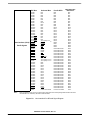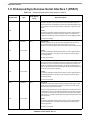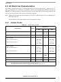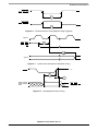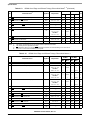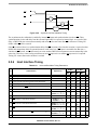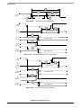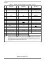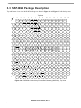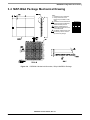
1
Freescale Semiconductor
Technical Data
DSP56301
Rev. 10, 7/2006
DSP56301
24-Bit Digital Signal Processor
52
6
6
3
Memory Expansion Area
Triple
Timer
Host
Interface
ESSI
SCI
X Data
Program
RAM
RAM
4096 × 24 bits 2048 × 24
bits
(Default)
(Default)
Y Data
RAM
2048 × 24
bits
(Default)
Peripheral
Expansion Area
24
External
Address
Bus
Switch
Bootstrap
ROM
DSP56300
Core
DDB
YDB
XDB
PDB
Power
Management
Clock
PLL
2
RESET
PINIT/NMI
Program
Interrupt
Controller
Program
Decode
Controller
Program
Address
Generator
Data ALU
24 × 24+56→ 56-bit MAC
Two 56-bit Accumulators
56-bit Barrel Shifter
JTAG
What’s New?
Rev. 10 includes the following
changes:
GDB
EXTAL
XTAL
24
External
Data
Bus
Data
Internal
Data
Bus
Switch
14
Control
External
Bus
Interface
and
I-Cache
Control
24-Bit
Address
YAB
XAB
PAB
DAB
Address
Generator
Unit
Six-Channel
DMA Unit
The DSP56301 is intended
for general-purpose digital
signal processing,
particularly in multimedia
and telecommunication
applications, such as video
conferencing and cellular
telephony.
6
• Removes all references to
Motorola. No specifications or
part numbers were changed.
OnCE™
MODD/IRQD
MODC/IRQC
MODB/IRQB
MODA/IRQA
Figure 1. DSP56301 Block Diagram
The DSP56301 is a member of the DSP56300 core family of programmable CMOS Digital Signal Processors
(DSPs). This family uses a high-performance, single clock cycle per instruction engine. Significant architectural
features of the DSP56300 core family include a barrel shifter, 24-bit addressing, instruction cache, and DMA. The
DSP56301 offers 80/100 MIPS using an internal 80/100 MHz clock at 3.0–3.6 volts. The DSP56300 core family
offers a rich instruction set and low power dissipation, as well as increasing levels of speed and power, enabling
wireless, telecommunications, and multimedia products.
© Freescale Semiconductor, Inc., 1996, 2006. All rights reserved.
Table of Contents
DSP56301 Features.............................................................................................................................................iii
Target Applications.............................................................................................................................................iv
Product Documentation ......................................................................................................................................iv
Chapter 1
Signals/Connections
1.1
1.2
1.3
1.4
1.5
1.6
1.7
1.8
1.9
1.10
1.11
1.12
Chapter 2
Specifications
2.1
2.2
2.3
2.4
2.5
Chapter 3
TQFP Package Description...............................................................................................................................3-2
TQFP Package Mechanical Drawing..............................................................................................................3-11
MAP-BGA Package Description ....................................................................................................................3-12
MAP-BGA Package Mechanical Drawing .....................................................................................................3-23
Design Considerations
4.1
4.2
4.3
4.4
4.5
Chapter A
Maximum Ratings.............................................................................................................................................2-1
Absolute Maximum Ratings .............................................................................................................................2-2
Thermal Characteristics ....................................................................................................................................2-2
DC Electrical Characteristics............................................................................................................................2-2
AC Electrical Characteristics............................................................................................................................2-4
Packaging
3.1
3.2
3.3
3.4
Chapter 4
Power ................................................................................................................................................................1-4
Ground ..............................................................................................................................................................1-4
Clock.................................................................................................................................................................1-5
Phase Lock Loop (PLL)....................................................................................................................................1-5
External Memory Expansion Port (Port A) ......................................................................................................1-6
Interrupt and Mode Control ..............................................................................................................................1-9
Host Interface (HI32)......................................................................................................................................1-10
Enhanced Synchronous Serial Interface 0 (ESSI0) ........................................................................................1-16
Enhanced Synchronous Serial Interface 1 (ESSI1) ........................................................................................1-18
Serial Communication Interface (SCI) ...........................................................................................................1-19
Timers .............................................................................................................................................................1-20
JTAG/OnCE Interface.....................................................................................................................................1-21
Thermal Design Considerations........................................................................................................................4-1
Electrical Design Considerations......................................................................................................................4-2
Power Consumption Considerations.................................................................................................................4-3
PLL Performance Issues ...................................................................................................................................4-4
Input (EXTAL) Jitter Requirements .................................................................................................................4-4
Power Consumption Benchmark
Index
Data Sheet Conventions
OVERBAR
Indicates a signal that is active when pulled low (For example, the RESET pin is active when
low.)
“asserted”
Means that a high true (active high) signal is high or that a low true (active low) signal is low
“deasserted”
Means that a high true (active high) signal is low or that a low true (active low) signal is high
Examples:
Signal/Symbol
Logic State
Signal State
Voltage
PIN
VIL/VOL
True
Asserted
PIN
VIH/VOH
False
Deasserted
PIN
VIH/VOH
True
Asserted
PIN
VIL/VOL
False
Deasserted
Note: Values for VIL, VOL, VIH, and VOH are defined by individual product specifications.
DSP56301 Technical Data, Rev. 10
ii
Freescale Semiconductor
DSP56301 Features
High-Performance DSP56300 Core
• 80/100 million instructions per second (MIPS) with a 80/100 MHz clock at 3.0–3.6 V
• Object code compatible with the DSP56000 core with highly parallel instruction set
• Data Arithmetic Logic Unit (Data ALU) with fully pipelined 24 × 24-bit parallel MultiplierAccumulator (MAC), 56-bit parallel barrel shifter (fast shift and normalization; bit stream
generation and parsing), conditional ALU instructions, and 24-bit or 16-bit arithmetic support
under software control
• Program Control Unit (PCU) with Position Independent Code (PIC) support, addressing modes
optimized for DSP applications (including immediate offsets), internal instruction cache
controller, internal memory-expandable hardware stack, nested hardware DO loops, and fast
auto-return interrupts
• Direct Memory Access (DMA) with six DMA channels supporting internal and external
accesses; one-, two-, and three-dimensional transfers (including circular buffering); end-ofblock-transfer interrupts; and triggering from interrupt lines and all peripherals
• Phase Lock Loop (PLL) allows change of low-power Divide Factor (DF) without loss of lock
and output clock with skew elimination
• Hardware debugging support including On-Chip Emulation (OnCE™) module, Joint Test Action
Group (JTAG) Test Access Port (TAP)
Internal Peripherals
• 32-bit parallel PCI/Universal Host Interface (HI32), PCI Rev. 2.1 compliant with glueless
interface to other DSP563xx buses or ISA interface requiring only 74LS45-style buffers
• Two enhanced synchronous serial interfaces (ESSI), each with one receiver and three
transmitters (allows six-channel home theater)
• Serial communications interface (SCI) with baud rate generator
• Triple timer module
• Up to forty-two programmable general-purpose input/output (GPIO) pins, depending on which
peripherals are enabled
Internal Memories
• 3 K × 24-bit bootstrap ROM
• 8 K × 24-bit internal RAM total
• Program RAM, Instruction Cache, X data RAM, and Y data RAM sizes are programmable:
Program RAM Instruction Cache
X Data RAM Size Y Data RAM Size
Size
Size
Instruction
Cache
Switch
Mode
4096 × 24 bits
0
2048 × 24 bits
2048 × 24 bits
disabled
disabled
3072 × 24 bits
1024 × 24-bit
2048 × 24 bits
2048 × 24 bits
enabled
disabled
2048 × 24 bits
0
3072 × 24 bits
3072 × 24 bits
disabled
enabled
1024 × 24 bits
1024 × 24-bit
3072 × 24 bits
3072 × 24 bits
enabled
enabled
DSP56301 Technical Data, Rev. 10
Freescale Semiconductor
iii
External Memory Expansion
• Data memory expansion to two 16 M × 24-bit word memory spaces in 24-Bit mode or two 64 K
× 16-bit memory spaces in 16-Bit Compatibility mode
• Program memory expansion to one 16 M × 24-bit words memory space in 24-Bit mode or 64 K ×
16-bit in 16-Bit Compatibility mode
• External memory expansion port
• Chip Select Logic for glueless interface to SRAMs
• Internal DRAM Controller for glueless interface to dynamic random access memory (DRAMs)
Reduced Power Dissipation
•
•
•
•
Very low-power CMOS design
Wait and Stop low-power standby modes
Fully static design specified to operate down to 0 Hz (dc)
Optimized power management circuitry (instruction-dependent, peripheral-dependent, and
mode-dependent)
Packaging
The DSP56301 is available in a 208-pin thin quad flat pack (TQFP) or a 252-pin molded array
process-ball grid array (MAP-BGA) package. Both packages are available in lead-bearing and
lead-free versions.
Target Applications
Examples of target applications include:
•
•
•
•
•
Wireless and wireline infrastructure applications
Multi-channel wireless local loop systems
DSP resource boards
High-speed modem banks
Packet telephony
Product Documentation
The three documents listed in the following table are required for a complete description of the
DSP56301 and are necessary to design properly with the part. Documentation is available from the
following sources. (See the back cover for detailed information.)
•
•
•
•
A local Freescale distributor
A Freescale semiconductor sales office
A Freescale Literature Distribution Center
The World Wide Web (WWW)
Table 1.
Name
DSP56301 Documentation
Description
Order Number
DSP56300 Family
Manual
Detailed description of the DSP56300 family processor core and
instruction set
DSP56300FM/AD
DSP56301 User’s
Manual
Detailed functional description of the DSP56301 memory
configuration, operation, and register programming
DSP56301UM/D
DSP56301
Technical Data
DSP56301 features list and physical, electrical, timing, and
package specifications
DSP56301
DSP56301 Technical Data, Rev. 10
iv
Freescale Semiconductor
1
Signals/Connections
The DSP56301 input and output signals are organized into functional groups, as shown in Table 1-1 and illustrated
in Figure 1-1. The DSP56301 operates from a 3 V supply; however, some of the inputs can tolerate 5 V. A special
notice for this feature is added to the signal descriptions of those inputs.
Table 1-1.
DSP56301 Functional Signal Groupings
Number of
Signals by
Package Type
Functional Group
Detailed Description
TQFP
MAPBGA
Power (VCC)1
25
45
Table 1-2
Ground (GND)1
26
38
Table 1-3
Clock
2
2
Table 1-4
PLL
3
3
Table 1-5
24
24
Table 1-6
Data Bus
24
24
Table 1-7
Bus Control
15
15
Table 1-8
Interrupt and Mode Control
5
5
Table 1-9
Port B3
52
52
Table 1-11
Ports C and D4
12
12
Table 1-12 and
Table 1-13
Port E5
3
3
Table 1-14
Timer
3
3
Table 1-15
JTAG/OnCE Port
6
6
Table 1-16
Address Bus
Port A2
Host Interface (HI32)
Enhanced Synchronous Serial Interface (ESSI)
Serial Communication Interface (SCI)
Notes:
1.
2.
3.
4.
5.
6.
The number of available power and ground signals is package-dependent. In the TQFP package specific pins are dedicated
internally to device subsystems. In the MAP-BGA package, power and ground connections (except those providing PLL
power) connect to internal power and ground planes, respectively.
Port A signals define the external memory interface port, including the external address bus, data bus, and control signals.
Port B signals are the HI32 port signals multiplexed with the GPIO signals.
Port C and D signals are the two ESSI port signals multiplexed with the GPIO signals.
Port E signals are the SCI port signals multiplexed with the GPIO signals.
Each device also includes several no connect (NC) pins. The number of NC connections is package-dependent: the TQFP
has 9 NCs and the MAP-BGA has 20 NCs. Do not connect any line, component, trace, or via to these pins. See Chapter 3
for details.
DSP56301 Technical Data, Rev. 10
Freescale Semiconductor
1-1
Signals/Connections
DSP56301
VCCP
VCCQ
VCCA
VCCD
VCCN
VCCH
VCCS
Power Inputs :
PLL
Internal Logic
Address Bus
Data Bus
Bus Control
HI32
ESSI/SCI/Timer
4
6
4
2
6
2
GNDP
GNDP1
GNDQ
GNDA
GNDD
GNDN
GNDH
GNDS
PCI Bus
Host
Interface
(HI32) Port2
Grounds1:
PLL
PLL
Internal Logic
Address Bus
Data Bus
Bus Control
HI32
ESSI/SCI/Timer
4
6
4
2
6
2
EXTAL
XTAL
Clock
CLKOUT
PCAP
PINIT/NMI
52
Extended Synchronous
Serial Interface Port 0
(ESSI0)3
3
Extended
Synchronous Serial
Interface Port 1
(ESSI1)3
3
Universal
Bus
A[0-23]
D[0-23]
AA[0–3]
RAS[0–3]
RD
WR
BS
TA
BR
BG
BB
BL
CAS
BCLK
BCLK
24
External
Address Bus
24
External
Data Bus
4
Serial
Communications
Interface (SCI) Port3
External
Bus
Control
Timers4
JTAG/OnC
E Port
1.
2.
3.
4.
Port B
GPIO
See Figure 1-2 for a listing of the
Host Interface/Port B Signals
SC[00-02]
SCK0
SRD0
STD0
Port C GPIO
PC[0-2]
PC3
PC4
PC5
SC[10-12]
SCK1
SRD1
STD1
Port D GPIO
PD[0-2]
PD3
PD4
PD5
RXD
TXD
SCLK
Port E GPIO
PE0
PE1
PE2
PLL
Port A
Notes:
MODA/IRQA
MODB/IRQB
MODC/IRQC
MODD/IRQD
RESET
Interrupt
/Mode
Control
1
TIO0
TIO1
TIO2
Timer GPIO
TIO0
TIO1
TIO2
TCK
TDI
TDO
TMS
TRST
DE
Power and ground connections are shown for the TQFP package. The MAP-BGA package uses one
VCCP for the PLL power input and 44 VCC pins that connect to an internal power plane. The MAPBGA package uses two ground connections for the PLL (GNDP and GNDP1) and 36 GND pins that
connect to an internal ground plane.
The HI32 port supports PCI and non-PCI bus configurations. Twenty-four HI32 signals can also be
configured as GPIO signals (PB[0–23]).
The ESSI0, ESSI1, and SCI signals are multiplexed with the Port C GPIO signals (PC[0–5]), Port D
GPIO signals (PD[0–5]), and Port E GPIO signals (PE[0–2]), respectively.
TIO[0–2] can be configured as GPIO signals.
Figure 1-1.
Signals Identified by Functional Group
DSP56301 Technical Data, Rev. 10
1-2
Freescale Semiconductor
DSP56301
Host Interface (HI32)/
Port B Signals
Note:
PCI Bus
Universal Bus
Port B GPIO
HAD0
HAD1
HAD2
HAD3
HAD4
HAD5
HAD6
HAD7
HAD8
HAD9
HAD10
HAD11
HAD12
HAD13
HAD14
HAD15
HC0/HBE0
HC1/HBE1
HC2/HBE2
HC3/HBE3
HTRDY
HIRDY
HDEVSEL
HLOCK
HPAR
HPERR
HGNT
HREQ
HSERR
HSTOP
HIDSEL
HFRAME
HCLK
HAD16
HAD17
HAD18
HAD19
HAD20
HAD21
HAD22
HAD23
HAD24
HAD25
HAD26
HAD27
HAD28
HAD29
HAD30
HAD31
HRST
HINTA
PVCL
HA3
HA4
HA5
HA6
HA7
HA8
HA9
HA10
HD0
HD1
HD2
HD3
HD4
HD5
HD6
HD7
HA0
HA1
HA2
Tie to pull-up or VCC
HDBEN
HDBDR
HSAK
HBS
HDAK
HDRQ
HAEN
HTA
HIRQ
HWR/HRW
HRD/HDS
Tie to pull-up or VCC
Tie to pull-up or VCC
HD8
HD9
HD10
HD11
HD12
HD13
HD14
HD15
HD16
HD17
HD18
HD19
HD20
HD21
HD22
HD23
HRST
HINTA
Leave unconnected
PB0
PB1
PB2
PB3
PB4
PB5
PB6
PB7
PB8
PB9
PB10
PB11
PB12
PB13
PB14
PB15
PB16
PB17
PB18
PB19
PB20
PB21
PB22
PB23
Internal disconnect
Internal disconnect
Internal disconnect
Internal disconnect
Internal disconnect
Internal disconnect
Internal disconnect
Internal disconnect
Internal disconnect
Internal disconnect
Internal disconnect
Internal disconnect
Internal disconnect
Internal disconnect
Internal disconnect
Internal disconnect
Internal disconnect
Internal disconnect
Internal disconnect
Internal disconnect
Internal disconnect
Internal disconnect
Internal disconnect
Internal disconnect
Internal disconnect
Internal disconnect
Internal disconnect
Leave unconnected
Host Port (HP)
Reference
HP0
HP1
HP2
HP3
HP4
HP5
HP6
HP7
HP8
HP9
HP10
HP11
HP12
HP13
HP14
HP15
HP16
HP17
HP18
HP19
HP20
HP21
HP22
HP23
HP24
HP25
HP26
HP27
HP28
HP29
HP30
HP31
HP32
HP33
HP34
HP35
HP36
HP37
HP38
HP39
HP40
HP41
HP42
HP43
HP44
HP45
HP46
HP47
HP48
HP49
HP50
PVCL
HPxx is a reference only and is not a signal name. GPIO references formerly designated as HIOxx have been
renamed PBxx for consistency with other Freescale DSPs.
Figure 1-2.
Host Interface/Port B Detail Signal Diagram
DSP56301 Technical Data, Rev. 10
Freescale Semiconductor
1-3
Signals/Connections
1.1 Power
Table 1-2.
Power Name
Power Inputs
Description
VCCP
PLL Power
Isolated power for the Phase Lock Loop (PLL). The voltage should be well-regulated and the input should be provided
with an extremely low impedance path to the VCC power rail.
VCCQ
Quiet Power
Isolated power for the internal processing logic. This input must be tied externally to all other chip power inputs. The
user must provide adequate external decoupling capacitors.
VCCA
Address Bus Power
Isolated power for sections of the address bus I/O drivers. This input must be tied externally to all other chip power
inputs. The user must provide adequate external decoupling capacitors.
VCCD
Data Bus Power
Isolated power for sections of the data bus I/O drivers. This input must be tied externally to all other chip power inputs.
The user must provide adequate external decoupling capacitors.
VCCN
Bus Control Power
Isolated power for the bus control I/O drivers. This input must be tied externally to all other chip power inputs. The user
must provide adequate external decoupling capacitors.
VCCH
Host Power
Isolated power for the HI32 I/O drivers. This input must be tied externally to all other chip power inputs. The user must
provide adequate external decoupling capacitors.
VCCS
ESSI, SCI, and Timer Power
Isolated power for the ESSI, SCI, and timer I/O drivers. This input must be tied externally to all other chip power inputs.
The user must provide adequate external decoupling capacitors.
Note:
These designations are package-dependent. Some packages connect all VCC inputs except VCCP to each other internally. On
those packages, all power input except VCCP are labeled VCC.
1.2 Ground
Table 1-3.
Ground Name
Grounds
Description
GNDP
PLL Ground
Ground dedicated for PLL use. The connection should be provided with an extremely low-impedance path to ground.
VCCP should be bypassed to GNDP by a 0.47 μF capacitor located as close as possible to the chip package.
GNDP1
PLL Ground 1
Ground dedicated for PLL use. The connection should be provided with an extremely low-impedance path to ground.
GNDQ
Quiet Ground
Isolated ground for the internal processing logic. This connection must be tied externally to all other chip ground
connections. The user must provide adequate external decoupling capacitors.
GNDA
Address Bus Ground
Isolated ground for sections of the address bus I/O drivers. This connection must be tied externally to all other chip
ground connections. The user must provide adequate external decoupling capacitors.
GNDD
Data Bus Ground
Isolated ground for sections of the data bus I/O drivers. This connection must be tied externally to all other chip ground
connections. The user must provide adequate external decoupling capacitors.
DSP56301 Technical Data, Rev. 10
1-4
Freescale Semiconductor
Clock
Table 1-3.
Ground Name
Grounds
Description
GNDN
Bus Control Ground
Isolated ground for the bus control I/O drivers. This connection must be tied externally to all other chip ground
connections. The user must provide adequate external decoupling capacitors.
GNDH
Host Ground
Isolated ground for the HI32 I/O drivers. This connection must be tied externally to all other chip ground connections.
The user must provide adequate external decoupling capacitors.
GNDS
ESSI, SCI, and Timer Ground
Isolated ground for the ESSI, SCI, and timer I/O drivers. This connection must be tied externally to all other chip ground
connections. The user must provide adequate external decoupling capacitors.
Note:
These designations are package-dependent. Some packages connect all GND inputs except GNDP and GNDP1 to each other
internally. On those packages, all ground connections except GNDP and GNDP1 are labeled GND.
1.3 Clock
Table 1-4.
Signal Name
Type
State During
Reset
Clock Signals
Signal Description
EXTAL
Input
Input
External Clock/Crystal Input
Interfaces the internal crystal oscillator input to an external crystal or an
external clock.
XTAL
Output
Chip-driven
Crystal Output
Connects the internal crystal oscillator output to an external crystal. If an
external clock is used, leave XTAL unconnected.
1.4 Phase Lock Loop (PLL)
Table 1-5.
Signal Name
CLKOUT
Type
Output
State During
Reset
Chip-driven
Phase Lock Loop Signals
Signal Description
Clock Output
Provides an output clock synchronized to the internal core clock phase.
If the PLL is enabled and both the multiplication and division factors equal one,
then CLKOUT is also synchronized to EXTAL.
If the PLL is disabled, the CLKOUT frequency is half the frequency of EXTAL.
PCAP
Input
Input
PLL Capacitor
Connects an off-chip capacitor to the PLL filter. Connect one capacitor
terminal to PCAP and the other terminal to VCCP.
If the PLL is not used, PCAP can be tied to VCC, GND, or left floating.
DSP56301 Technical Data, Rev. 10
Freescale Semiconductor
1-5
Signals/Connections
Table 1-5.
Signal Name
PINIT/NMI
Type
Input
Phase Lock Loop Signals (Continued)
State During
Reset
Signal Description
Input
PLL Initial/Non-Maskable Interrupt
During assertion of RESET, the value of PINIT/NMI is written into the PLL
Enable (PEN) bit of the PLL control register, determining whether the PLL is
enabled or disabled. After RESET deassertion and during normal instruction
processing, the PINIT/NMI Schmitt-trigger input is a negative-edge-triggered
Non-Maskable Interrupt (NMI) request internally synchronized to CLKOUT.
PINIT/NMI can tolerate 5 V.
1.5 External Memory Expansion Port (Port A)
Note: When the DSP56301 enters a low-power stand-by mode (Stop or Wait), it releases bus mastership and tristates the relevant Port A signals: A[0–23], D[0–23], AA0/RAS0–AA3/RAS3, RD, WR, BB, CAS, BCLK, and
BCLK. If hardware refresh of external DRAM is enabled, Port A exits the Wait mode to allow the refresh to
occur and then returns to the Wait mode.
1.5.1
External Address Bus
Table 1-6.
Signal Name
A[0–23]
1.5.2
Type
Output
State During
Reset
Tri-stated
Signal Description
Address Bus
When the DSP is the bus master, A[0–23] specify the address for external
program and data memory accesses. Otherwise, the signals are tri-stated. To
minimize power dissipation, A[0–23] do not change state when external
memory spaces are not being accessed.
External Data Bus
Table 1-7.
Signal Name
D[0–23]
External Address Bus Signals
Type
Input/Output
State During
Reset
Tri-stated
External Data Bus Signals
Signal Description
Data Bus
When the DSP is the bus master, D[0–23] provide the bidirectional data bus
for external program and data memory accesses. Otherwise, D[0–23] are tristated.
DSP56301 Technical Data, Rev. 10
1-6
Freescale Semiconductor
External Memory Expansion Port (Port A)
1.5.3
External Bus Control
Table 1-8.
Signal Name
Type
State During
Reset
External Bus Control Signals
Signal Description
AA0/RAS0–
AA3/RAS3
Output
Tri-stated
Address Attribute or Row Address Strobe
As AA, these signals function as chip selects or additional address lines.
Unlike address lines, however, the AA lines do not hold their state after a read
or write operation. As RAS, these signals can be used for Dynamic Random
Access Memory (DRAM) interface. These signals have programmable
polarity.
RD
Output
Tri-stated
Read Enable
When the DSP is the bus master, RD is asserted to read external memory on
the data bus (D[0–23]). Otherwise, RD is tri-stated.
WR
Output
Tri-stated
Write Enable
When the DSP is the bus master, WR is asserted to write external memory on
the data bus (D[0–23]). Otherwise, WR is tri-stated.
TA
Input
Ignored Input
Transfer Acknowledge
If the DSP56301 is the bus master and there is no external bus activity, or the
DSP56301 is not the bus master, the TA input is ignored. The TA input is a
Data Transfer Acknowledge (DTACK) function that can extend an external bus
cycle indefinitely. Any number of wait states (1, 2,..., infinity) can be added to
the wait states inserted by the BCR by keeping TA deasserted. In typical
operation, TA is deasserted at the start of a bus cycle, asserted to enable
completion of the bus cycle, and deasserted before the next bus cycle. The
current bus cycle completes one clock period after TA is asserted
synchronous to CLKOUT. The number of wait states is determined by the TA
input or by the Bus Control Register (BCR), whichever is longer. The BCR can
set the minimum number of wait states in external bus cycles.
To use the TA functionality, the BCR must be programmed to at least one wait
state. A zero wait state access cannot be extended by TA deassertion;
otherwise improper operation may result. TA can operate synchronously or
asynchronously, depending on the setting of the TAS bit in the Operating
Mode Register (OMR).
TA functionality cannot be used during DRAM-type accesses; otherwise
improper operation may result.
BR
Output
Output
(deasserted)
Bus Request
Asserted when the DSP requests bus mastership and deasserted when the
DSP no longer needs the bus. BR can be asserted or deasserted
independently of whether the DSP56301 is a bus master or a bus slave. Bus
“parking” allows BR to be deasserted even though the DSP56301 is the bus
master (see the description of bus “parking” in the BB signal description). The
Bus Request Hole (BRH) bit in the BCR allows BR to be asserted under
software control, even though the DSP does not need the bus. BR is typically
sent to an external bus arbitrator that controls the priority, parking and tenure
of each master on the same external bus. BR is affected only by DSP requests
for the external bus, never for the internal bus. During hardware reset, BR is
deasserted and the arbitration is reset to the bus slave state.
BG
Input
Ignored Input
Bus Grant
Must be asserted/deasserted synchronous to CLKOUT for proper operation.
An external bus arbitration circuit asserts BG when the DSP56301 becomes
the next bus master. When BG is asserted, the DSP56301 must wait until BB
is deasserted before taking bus mastership. When BG is deasserted, bus
mastership is typically given up at the end of the current bus cycle. This may
occur in the middle of an instruction that requires more than one external bus
cycle for execution.
DSP56301 Technical Data, Rev. 10
Freescale Semiconductor
1-7
Signals/Connections
Table 1-8.
Signal Name
BB
Type
Input/
Output
External Bus Control Signals (Continued)
State During
Reset
Input
Signal Description
Bus Busy
Indicates that the bus is active and must be asserted and deasserted
synchronous to CLKOUT. Only after BB is deasserted can the pending bus
master become the bus master (and then assert the signal again). The bus
master can keep BB asserted after ceasing bus activity, regardless of whether
BR is asserted or deasserted. This is called “bus parking” and allows the
current bus master to reuse the bus without re-arbitration until another device
requires the bus. BB is deasserted by an “active pull-up” method (that is, BB is
driven high and then released and held high by an external pull-up resistor).
BB requires an external pull-up resistor.
BL
Output
Driven high
(deasserted)
Bus Lock—BL is asserted at the start of an external divisible Read-ModifyWrite (RMW) bus cycle, remains asserted between the read and write cycles,
and is deasserted at the end of the write bus cycle. This provides an “early bus
start” signal for the bus controller. BL may be used to “resource lock” an
external multi-port memory for secure semaphore updates. Early deassertion
provides an “early bus end” signal useful for external bus control. If the
external bus is not used during an instruction cycle, BL remains deasserted
until the next external indivisible RMW cycle. The only instructions that assert
BL automatically are the BSET, CLR, and BCHG instructions when they are
used to modify external memory. An operation can also assert BL by setting
the BLH bit in the Bus Control Register.
CAS
Output
Tri-stated
Column Address Strobe
When the DSP is the bus master, DRAM uses CAS to strobe the column
address. Otherwise, if the Bus Mastership Enable (BME) bit in the DRAM
Control Register is cleared, the signal is tri-stated.
BCLK
Output
Tri-stated
Bus Clock
When the DSP is the bus master, BCLK is active when the OMR[ATE] is set.
When BCLK is active and synchronized to CLKOUT by the internal PLL, BCLK
precedes CLKOUT by one-fourth of a clock cycle.
BCLK
Output
Tri-stated
Bus Clock Not
When the DSP is the bus master, BCLK is the inverse of the BCLK signal.
Otherwise, the signal is tri-stated.
DSP56301 Technical Data, Rev. 10
1-8
Freescale Semiconductor
Interrupt and Mode Control
1.6 Interrupt and Mode Control
The interrupt and mode control signals select the chip’s operating mode as it comes out of hardware reset. After
RESET is deasserted, these inputs are hardware interrupt request lines.
Table 1-9.
Signal Name
Type
MODA
Input
IRQA
Input
State During
Reset
Input
Interrupt and Mode Control
Signal Description
Mode Select A
Selects the initial chip operating mode during hardware reset and becomes a
level-sensitive or negative-edge-triggered, maskable interrupt request input
IRQA during normal instruction processing. MODA, MODB, MODC, and
MODD select one of sixteen initial chip operating modes, latched into the OMR
when the RESET signal is deasserted.
External Interrupt Request A
Internally synchronized to CLKOUT. If IRQA is asserted synchronous to
CLKOUT, multiple processors can be re-synchronized using the WAIT
instruction and asserting IRQA to exit the Wait state. If the processor is in the
Stop stand-by state and IRQA is asserted, the processor exits the Stop state.
These inputs are 5 V tolerant.
MODB
Input
IRQB
Input
Input
Mode Select B
Selects the initial chip operating mode during hardware reset and becomes a
level-sensitive or negative-edge-triggered, maskable interrupt request input
IRQB during normal instruction processing. MODA, MODB, MODC, and
MODD select one of sixteen initial chip operating modes, latched into the OMR
when the RESET signal is deasserted.
External Interrupt Request B
Internally synchronized to CLKOUT. If IRQB is asserted synchronous to
CLKOUT, multiple processors can be re-synchronized using the WAIT
instruction and asserting IRQB to exit the Wait state. If the processor is in the
Stop stand-by state and IRQC is asserted, the processor will exit the Stop
state.
These inputs are 5 V tolerant.
MODC
Input
IRQC
Input
Input
Mode Select C
Selects the initial chip operating mode during hardware reset and becomes a
level-sensitive or negative-edge-triggered, maskable interrupt request input
IRQC during normal instruction processing. MODA, MODB, MODC, and
MODD select one of sixteen initial chip operating modes, latched into the OMR
when the RESET signal is deasserted.
External Interrupt Request C
Internally synchronized to CLKOUT. If IRQC is asserted synchronous to
CLKOUT, multiple processors can be re-synchronized using the WAIT
instruction and asserting IRQC to exit the Wait state. If the processor is in the
Stop stand-by state and IRQC is asserted, the processor exits the Stop state.
These inputs are 5 V tolerant.
DSP56301 Technical Data, Rev. 10
Freescale Semiconductor
1-9
Signals/Connections
Table 1-9.
Signal Name
Type
MODD
Input
IRQD
Input
Interrupt and Mode Control (Continued)
State During
Reset
Signal Description
Input
Mode Select D
Selects the initial chip operating mode during hardware reset and becomes a
level-sensitive or negative-edge-triggered, maskable interrupt request input
IRQD during normal instruction processing. MODA, MODB, MODC, and
MODD select one of sixteen initial chip operating modes, latched into the OMR
when the RESET signal is deasserted.
External Interrupt Request D
Internally synchronized to CLKOUT. If IRQD is asserted synchronous to
CLKOUT, multiple processors can be re-synchronized using the WAIT
instruction and asserting IRQD to exit the Wait state. If the processor is in the
Stop stand-by state and IRQD is asserted, the processor exits the Stop state.
These inputs are 5 V tolerant.
RESET
Input
Input
Reset
Deassertion of RESET is internally synchronized to the clock out (CLKOUT).
When asserted, the chip is placed in the Reset state and the internal phase
generator is reset. The Schmitt-trigger input allows a slowly rising input (such
as a capacitor charging) to reset the chip reliably. If RESET is deasserted
synchronous to CLKOUT, exact start-up timing is guaranteed, allowing
multiple processors to start synchronously and operate together in “lock-step.”
When the RESET signal is deasserted, the initial chip operating mode is
latched from the MODA, MODB, MODC, and MODD inputs. The RESET
signal must be asserted after power-up.
This input is 5 V tolerant.
1.7 Host Interface (HI32)
The Host Interface (HI32) provides fast parallel data to a 32-bit port directly connected to the host bus. The HI32
supports a variety of standard buses and directly connects to a PCI bus and a number of industry-standard
microcomputers, microprocessors, DSPs, and DMA hardware.
1.7.1
Host Port Usage Considerations
Careful synchronization is required when the system reads multiple-bit registers that are written by another
asynchronous system. This is a common problem when two asynchronous systems are connected (as they are in the
Host port). The considerations for proper operation are discussed in Table 1-10.
Table 1-10.
Action
Host Port Usage Considerations
Description
Asynchronous read of
receive byte registers
When reading the receive byte registers, Receive register High (RXH), Receive register Middle (RXM), or
Receive register Low (RXL), use interrupts or poll the Receive register Data Full (RXDF) flag that indicates
data is available. This assures that the data in the receive byte registers is valid.
Asynchronous write to
transmit byte registers
Do not write to the transmit byte registers, Transmit register High (TXH), Transmit register Middle (TXM), or
Transmit register Low (TXL), unless the Transmit register Data Empty (TXDE) bit is set, indicating that the
transmit byte registers are empty. This guarantees that the transmit byte registers transfer valid data to the
Host Receive (HRX) register.
DSP56301 Technical Data, Rev. 10
1-10
Freescale Semiconductor
Host Interface (HI32)
Table 1-10.
Host Port Usage Considerations (Continued)
Action
Description
Asynchronous write to host
vector
1.7.2
Change the Host Vector (HV) register only when the Host Command bit (HC) is clear. This practice
guarantees that the DSP interrupt control logic receives a stable vector.
Host Port Configuration
HI32 signal functions vary according to the programmed configuration of the interface as determined by the 24-bit
DSP Control Register (DCTR). Refer to the DSP56301 User’s Manual for details on HI32 configuration registers.
Table 1-11.
Signal Name
Type
State During
Reset
Tri-stated
Host Interface
Signal Description
HAD[0–7]
Input/Output
Host Address/Data 0–7
When the HI32 is programmed to interface with a PCI bus and the HI function
is selected, these signals are lines 0–7 of the Address/Data bus.
HA[3–10]
Input
Host Address 3–10
When HI32 is programmed to interface with a universal, non-PCI bus and the
HI function is selected, these signals are lines 3–10 of the Address bus.
PB[0–7]
Input or Output
Port B 0–7
When the HI32 is configured as GPIO through the DCTR, these signals are
individually programmed through the HI32 Data Direction Register (DIRH).
These inputs are 5 V tolerant.
HAD[8–15]
Input/Output
Tri-stated
Host Address/Data 8–15
When the HI32 is programmed to interface with a PCI bus and the HI function
is selected, these signals are lines 8–15 of the Address/Data bus.
HD[0–7]
Input/Output
Host Data 0–7
When HI32 is programmed to interface with a universal non-PCI bus and the
HI function is selected, these signals are lines 0–7 of the Data bus.
PB[8–15]
Input or Output
Port B 8–15
When the HI32 is configured as GPIO through the DCTR, these signals are
individually programmed through the HI32 DIRH.
These inputs are 5 V tolerant.
HC[0–3]/
HBE[0–3]
Input/Output
HA[0–2]
Input
Tri-stated
Command 0–3/Byte Enable 0–3
When the HI32 is programmed to interface with a PCI bus and the HI function
is selected, these signals are lines 0–7 of the Address/Data bus.
Host Address 0–2
When HI32 is programmed to interface with a universal, non-PCI bus and the
HI function is selected, these signals are lines 0–2 of the Address bus.
The fourth signal in this set should connect to a pull-up resistor or directly to
VCC when a non-PCI bus is used.
PB[16–19]
Input or Output
Port B 16–19
When the HI32 is configured as GPIO through the DCTR, these signals are
individually programmed through the HI32 DIRH.
These inputs are 5 V tolerant.
DSP56301 Technical Data, Rev. 10
Freescale Semiconductor
1-11
Signals/Connections
Table 1-11.
Signal Name
Type
Host Interface (Continued)
State During
Reset
Signal Description
HTRDY
Input/
Output
HDBEN
Output
Host Data Bus Enable
When HI32 is programmed to interface with a universal, non-PCI bus and the
HI function is selected, this is the Host Data Bus Enable signal.
PB20
Input or Output
Port B 20
When the HI32 is configured as GPIO through the DCTR, this signal is
individually programmed through the HI32 DIRH.
Tri-stated
Host Target Ready
When the HI32 is programmed to interface with a PCI bus and the HI function
is selected, this is the Host Target Ready signal.
This input is 5 V tolerant.
HIRDY
Input/
Output
Tri-stated
Host Initiator Ready
When the HI32 is programmed to interface with a PCI bus and the HI function
is selected, this is the Host Initiator Ready signal.
HDBDR
Output
Host Data Bus Direction
When HI32 is programmed to interface with a universal, non-PCI bus and the
HI function is selected, this is the Host Data Bus Direction signal.
PB21
Input or Output
Port B 21
When the HI32 is configured as GPIO through the DCTR, this signal is
individually programmed through the HI32 DIRH.
This input is 5 V tolerant.
HDEVSEL
Input/
Output
Tri-stated
Host Device Select
When the HI32 is programmed to interface with a PCI bus and the HI function
is selected, this is the Host Device Select signal.
HSAK
Output
Host Select Acknowledge
When HI32 is programmed to interface with a universal, non-PCI bus and the
HI function is selected, this is the Host Select Acknowledge signal.
PB22
Input or Output
Port B 22
When the HI32 is configured as GPIO through the DCTR, this signal is
individually programmed through the HI32 DIRH.
This input is 5 V tolerant.
HLOCK
Input
HBS
Input
Host Bus Strobe
When HI32 is programmed to interface with a universal, non-PCI bus and the
HI function is selected, this is the Host Bus Strobe Schmitt-trigger signal.
PB23
Input or Output
Port B 23
When the HI32 is configured as GPIO through the DCTR, this signal is
individually programmed through the HI32 DIRH.
Tri-stated
Host Lock
When the HI32 is programmed to interface with a PCI bus and the HI function
is selected, this is the Host Lock signal.
This input is 5 V tolerant.
DSP56301 Technical Data, Rev. 10
1-12
Freescale Semiconductor
Host Interface (HI32)
Table 1-11.
Signal Name
Type
HPAR
Input/
Output
HDAK
Input
Host Interface (Continued)
State During
Reset
Tri-stated
Signal Description
Host Parity
When the HI32 is programmed to interface with a PCI bus and the HI function
is selected, this is the Host Parity signal.
Host DMA Acknowledge
When HI32 is programmed to interface with a universal, non-PCI bus and the
HI function is selected, this is the Host DMA Acknowledge Schmitt-trigger
signal.
Port B
When the HI32 is configured as GPIO through the DCTR, this signal is
internally disconnected.
This input is 5 V tolerant.
HPERR
Input/
Output
HDRQ
Output
Tri-stated
Host Parity Error
When the HI32 is programmed to interface with a PCI bus and the HI function
is selected, this is the Host Parity Error signal.
Host DMA Request
When HI32 is programmed to interface with a universal, non-PCI bus and the
HI function is selected, this is the Host DMA Request output.
Port B
When the HI32 is configured as GPIO through the DCTR, this signal is
internally disconnected.
This input is 5 V tolerant.
HGNT
Input
HAEN
Input
Input
Host Bus Grant
When the HI32 is programmed to interface with a PCI bus and the HI function
is selected, this is the Host Bus Grant signal.
Host Address Enable
When HI32 is programmed to interface with a universal, non-PCI bus and the
HI function is selected, this is the Host Address Enable output signal.
Port B
When the HI32 is configured as GPIO through the DCTR, this signal is
internally disconnected.
This input is 5 V tolerant.
HREQ
Output
HTA
Output
Tri-stated
Host Bus Request
When the HI32 is programmed to interface with a PCI bus and the HI function
is selected, this is the Host Bus Request signal.
Host Transfer Acknowledge—When HI32 is programmed to interface with a
universal, non-PCI bus and the HI function is selected, this is the Host Data
Bus Enable signal. HTA can be programmed as active high or active low.
Port B
When the HI32 is configured as GPIO through the DCTR, this signal is
internally disconnected.
This input is 5 V tolerant.
DSP56301 Technical Data, Rev. 10
Freescale Semiconductor
1-13
Signals/Connections
Table 1-11.
Signal Name
Type
HSERR
Output, open
drain
HIRQ
Output, open
drain
Host Interface (Continued)
State During
Reset
Tri-stated
Signal Description
Host System Error
When the HI32 is programmed to interface with a PCI bus and the HI function
is selected, this is the Host System Error signal.
Host Interrupt Request
When HI32 is programmed to interface with a universal, non-PCI bus and the
HI function is selected, this is the Host Interrupt Request signal.
Port B
When the HI32 is configured as GPIO through the DCTR, this signal is
internally disconnected.
This input is 5 V tolerant.
HSTOP
Input/
Output
HWR/HRW
Input
Tri-stated
Host Stop
When the HI32 is programmed to interface with a PCI bus and the HI function
is selected, this is the Host Stop signal.
Host Write/Host Read-Write
When HI32 is programmed to interface with a universal, non-PCI bus and the
HI function is selected, this is the Host Write/Host Read-Write Schmitt-trigger
signal.
Port B
When the HI32 is configured as GPIO through the DCTR, this signal is
internally disconnected.
This input is 5 V tolerant.
HIDSEL
Input
HRD/HDS
Input
Input
Host Initialization Device Select
When the HI32 is programmed to interface with a PCI bus and the HI function
is selected, this is the Host Initialization Device Select signal.
Host Read/Host Data Strobe
When HI32 is programmed to interface with a universal, non-PCI bus and the
HI function is selected, this is the Host Data Read/Host Data Strobe Schmitttrigger signal.
Port B
When the HI32 is configured as GPIO through the DCTR, this signal is
internally disconnected.
This input is 5 V tolerant.
HFRAME
Input/
Output
Tri-stated
Host Frame
When the HI32 is programmed to interface with a PCI bus and the HI function
is selected, this is the Host cycle Frame signal.
Non-PCI bus
When HI32 is programmed to interface with a universal, non-PCI bus and the
HI function is selected, this signal must be connected to a pull-up resistor or
directly to VCC.
Port B
When the HI32 is configured as GPIO through the DCTR, this signal is
internally disconnected.
This input is 5 V tolerant.
DSP56301 Technical Data, Rev. 10
1-14
Freescale Semiconductor
Host Interface (HI32)
Table 1-11.
Signal Name
HCLK
Type
Input
Host Interface (Continued)
State During
Reset
Input
Signal Description
Host Clock
When the HI32 is programmed to interface with a PCI bus and the HI function
is selected, this is the Host Bus Clock input.
Non-PCI bus
When HI32 is programmed to interface a universal non-PCI bus and the HI
function is selected, this signal must be connected to a pull-up resistor or
directly to VCC.
Port B
When the HI32 is configured as GPIO through the DCTR, this signal is
internally disconnected.
This input is 5 V tolerant.
HAD[16–31]
Input/Output
HD[8–23]
Input/Output
Tri-stated
Host Address/Data 16–31
When the HI32 is programmed to interface with a PCI bus and the HI function
is selected, these signals are lines 16–31 of the Address/Data bus.
Host Data 8–23
When HI32 is programmed to interface with a universal, non-PCI bus and the
HI function is selected, these signals are lines 8–23 of the Data bus.
Port B
When the HI32 is configured as GPIO through the DCTR, these signals are
internally disconnected.
These inputs are 5 V tolerant.
HRST
Input
HRST
Input
Tri-stated
Hardware Reset
When the HI32 is programmed to interface with a PCI bus and the HI function
is selected, this is the Hardware Reset input.
Hardware Reset
When HI32 is programmed to interface with a universal, non-PCI bus and the
HI function is selected, this is the Hardware Reset Schmitt-trigger signal.
Port B
When the HI32 is configured as GPIO through the DCTR, this signal is
internally disconnected.
This input is 5 V tolerant.
HINTA
Output, open
drain
Tri-stated
Host Interrupt A
When the HI function is selected, this signal is the Interrupt A open-drain
output.
Port B
When the HI32 is configured as GPIO through the DCTR, this signal is
internally disconnected.
This input is 5 V tolerant.
PVCL
Input
Input
PCI Voltage Clamp
When the HI32 is programmed to interface with a PCI bus and the HI function
is selected and the PCI bus uses a 3 V signal environment, connect this pin to
VCC (3.3 V) to enable the high voltage clamping required by the PCI
specifications. In all other cases, including a 5 V PCI signal environment, leave
the input unconnected.
DSP56301 Technical Data, Rev. 10
Freescale Semiconductor
1-15
Signals/Connections
1.8 Enhanced Synchronous Serial Interface 0 (ESSI0)
Two synchronous serial interfaces (ESSI0 and ESSI1) provide a full-duplex serial port for serial communication
with a variety of serial devices, including one or more industry-standard codecs, other DSPs, microprocessors, and
peripherals that implement the Serial Peripheral Interface (SPI).
Table 1-12.
Signal Name
SC00
Type
Input or Output
Enhanced Synchronous Serial Interface 0 (ESSI0)
State During
Reset
Input
PC0
Signal Description
Serial Control 0
Functions in either Synchronous or Asynchronous mode. For Asynchronous
mode, this signal is the receive clock I/O (Schmitt-trigger input). For
Synchronous mode, this signal is either for Transmitter 1 output or Serial I/O
Flag 0.
Port C 0
The default configuration following reset is GPIO. For PC0, signal direction is
controlled through the Port Directions Register (PRR0). The signal can be
configured as ESSI signal SC00 through the Port Control Register (PCR0).
This input is 5 V tolerant.
SC01
Input/Output
PC1
Input or Output
Input
Serial Control 1
Functions in either Synchronous or Asynchronous mode. For Asynchronous
mode, this signal is the receiver frame sync I/O. For Synchronous mode, this
signal is either Transmitter 2 output or Serial I/O Flag 1.
Port C 1
The default configuration following reset is GPIO. For PC1, signal direction is
controlled through PRR0. The signal can be configured as an ESSI signal
SC01 through PCR0.
This input is 5 V tolerant.
SC02
Input/Output
PC2
Input or Output
Input
Serial Control Signal 2
The frame sync for both the transmitter and receiver in Synchronous mode,
and for the transmitter only in Asynchronous mode. When configured as an
output, this signal is the internally generated frame sync signal. When
configured as an input, this signal receives an external frame sync signal for
the transmitter (and the receiver in synchronous operation).
Port C 2
The default configuration following reset is GPIO. For PC2, signal direction is
controlled through PRR0. The signal can be configured as an ESSI signal
SC02 through PCR0.
This input is 5 V tolerant.
DSP56301 Technical Data, Rev. 10
1-16
Freescale Semiconductor
Enhanced Synchronous Serial Interface 0 (ESSI0)
Table 1-12.
Signal Name
SCK0
Type
Input/Output
Enhanced Synchronous Serial Interface 0 (ESSI0) (Continued)
State During
Reset
Input
Signal Description
Serial Clock
Provides the serial bit rate clock for the ESSI interface for both the transmitter
and receiver in Synchronous modes, or the transmitter only in Asynchronous
modes.
Although an external serial clock can be independent of and asynchronous to
the DSP system clock, it must exceed the minimum clock cycle time of 6 T
(that is, the system clock frequency must be at least three times the external
ESSI clock frequency). The ESSI needs at least three DSP phases inside
each half of the serial clock.
PC3
Input or Output
Port C 3
The default configuration following reset is GPIO. For PC3, signal direction is
controlled through PRR0. The signal can be configured as an ESSI signal
SCK0 through PCR0.
This input is 5 V tolerant.
SRD0
Input/Output
PC4
Input or Output
Input
Serial Receive Data
Receives serial data and transfers the data to the ESSI receive shift register.
SRD0 is an input when data is being received.
Port C 4
The default configuration following reset is GPIO. For PC4, signal direction is
controlled through PRR0. The signal can be configured as an ESSI signal
SRD0 through PCR0.
This input is 5 V tolerant.
STD0
Input/Output
PC5
Input or Output
Input
Serial Transmit Data
Transmits data from the serial transmit shift register. STD0 is an output when
data is being transmitted.
Port C 5
The default configuration following reset is GPIO. For PC5, signal direction is
controlled through PRR0. The signal can be configured as an ESSI signal
STD0 through PCR0.
This input is 5 V tolerant.
DSP56301 Technical Data, Rev. 10
Freescale Semiconductor
1-17
Signals/Connections
1.9 Enhanced Synchronous Serial Interface 1 (ESSI1)
Table 1-13.
Signal Name
SC10
Type
Input or Output
Enhanced Synchronous Serial Interface 1 (ESSI1)
State During
Reset
Input
PD0
Signal Description
Serial Control 0
Selection of Synchronous or Asynchronous mode determines function. For
Asynchronous mode, this signal is the receive clock I/O (Schmitt-trigger input).
For Synchronous mode, this signal is either Transmitter 1 output or Serial I/O
Flag 0.
Port D 0
The default configuration following reset is GPIO. For PD0, signal direction is
controlled through the Port Directions Register (PRR1). The signal can be
configured as an ESSI signal SC10 through the Port Control Register (PCR1).
This input is 5 V tolerant.
SC11
Input/Output
PD1
Input or Output
Input
Serial Control 1
Selection of Synchronous or Asynchronous mode determines function. For
Asynchronous mode, this signal is the receiver frame sync I/O. For
Synchronous mode, this signal is either Transmitter 2 output or Serial I/O Flag
1.
Port D 1
The default configuration following reset is GPIO. For PD1, signal direction is
controlled through PRR1. The signal can be configured as an ESSI signal
SC11 through PCR1.
This input is 5 V tolerant.
SC12
Input/Output
PD2
Input or Output
Input
Serial Control Signal 2
Frame sync for both the transmitter and receiver in Synchronous mode, for the
transmitter only in Asynchronous mode. When configured as an output, this
signal is the internally generated frame sync signal. When configured as an
input, this signal receives an external frame sync signal for the transmitter (and
the receiver in Synchronous operation).
Port D 2
The default configuration following reset is GPIO. For PD2, signal direction is
controlled through PRR1. The signal can be configured as an ESSI signal
SC12 through PCR1.
This input is 5 V tolerant.
SCK1
Input/Output
Input
Serial Clock
Provides the serial bit rate clock for the ESSI interface. Clock input or output
can be used by the transmitter and receiver in Synchronous modes, by the
transmitter only in Asynchronous modes.
Although an external serial clock can be independent of and asynchronous to
the DSP system clock, it must exceed the minimum clock cycle time of 6T (that
is, the system clock frequency must be at least three times the external ESSI
clock frequency). The ESSI needs at least three DSP phases inside each half
of the serial clock.
PD3
Input or Output
Port D 3
The default configuration following reset is GPIO. For PD3, signal direction is
controlled through PRR1. The signal can be configured as an ESSI signal
SCK1 through PCR1.
This input is 5 V tolerant.
DSP56301 Technical Data, Rev. 10
1-18
Freescale Semiconductor
Serial Communication Interface (SCI)
Table 1-13.
Signal Name
Type
SRD1
Input/Output
PD4
Input or Output
Enhanced Synchronous Serial Interface 1 (ESSI1) (Continued)
State During
Reset
Input
Signal Description
Serial Receive Data
Receives serial data and transfers it to the ESSI receive shift register. SRD1 is
an input when data is being received.
Port D 4
The default configuration following reset is GPIO. For PD4, signal direction is
controlled through PRR1. The signal can be configured as an ESSI signal
SRD1 through PCR1.
This input is 5 V tolerant.
STD1
Input/Output
PD5
Input or Output
Input
Serial Transmit Data
Transmits data from the serial transmit shift register. STD1 is an output when
data is being transmitted.
Port D 5
The default configuration following reset is GPIO. For PD5, signal direction is
controlled through PRR1. The signal can be configured as an ESSI signal
STD1 through PCR1.
This input is 5 V tolerant.
1.10 Serial Communication Interface (SCI)
The Serial Communication interface (SCI) provides a full duplex port for serial communication with other DSPs,
microprocessors, or peripherals such as modems.
Table 1-14.
Signal Name
Type
RXD
Input
PE0
Input or Output
Serial Communication Interface (SCI)
State During
Reset
Input
Signal Description
Serial Receive Data
Receives byte-oriented serial data and transfers it to the SCI receive shift
register.
Port E 0
The default configuration following reset is GPIO. When configured as PE0,
signal direction is controlled through the SCI Port Directions Register (PRR).
The signal can be configured as an SCI signal RXD through the SCI Port
Control Register (PCR).
This input is 5 V tolerant.
TXD
Output
PE1
Input or Output
Input
Serial Transmit Data
Transmits data from SCI transmit data register.
Port E 1
The default configuration following reset is GPIO. When configured as PE1,
signal direction is controlled through the SCI PRR. The signal can be
configured as an SCI signal TXD through the SCI PCR.
This input is 5 V tolerant.
DSP56301 Technical Data, Rev. 10
Freescale Semiconductor
1-19
Signals/Connections
Table 1-14.
Signal Name
Type
SCLK
Input/Output
PE2
Input or Output
Serial Communication Interface (SCI) (Continued)
State During
Reset
Input
Signal Description
Serial Clock
Provides the input or output clock used by the transmitter and/or the receiver.
Port E 2
The default configuration following reset is GPIO. For PE2, signal direction is
controlled through the SCI PRR. The signal can be configured as an SCI
signal SCLK through the SCI PCR.
This input is 5 V tolerant.
1.11 Timers
The DSP56301 has three identical and independent timers. Each can use internal or external clocking, interrupt the
DSP56301 after a specified number of events (clocks), or signal an external device after counting a specific number
of internal events.
Table 1-15.
Signal Name
TIO0
Type
Input or Output
Triple Timer Signals
State During
Reset
Input
Signal Description
Timer 0 Schmitt-Trigger Input/Output
As an external event counter or in Measurement mode, TIO0 is input. In
Watchdog, Timer, or Pulse Modulation mode, TIO0 is output.
The default mode after reset is GPIO input. This can be changed to output or
configured as a Timer Input/Output through the Timer 0 Control/Status
Register (TCSR0).
This input is 5 V tolerant.
TIO1
Input or Output
Input
Timer 1 Schmitt-Trigger Input/Output
As an external event counter or in Measurement mode, TIO1 is input. In
Watchdog, Timer, or Pulse Modulation mode, TIO1 is output.
The default mode after reset is GPIO input. This can be changed to output or
configured as a Timer Input/Output through the Timer 1 Control/Status
Register (TCSR1).
This input is 5 V tolerant.
TIO2
Input or Output
Input
Timer 2 Schmitt-Trigger Input/Output
As an external event counter or in Measurement mode, TIO2 is input. In
Watchdog, Timer, or Pulse Modulation mode, TIO2 is output.
The default mode after reset is GPIO input. This can be changed to output or
configured as a Timer Input/Output through the Timer 2 Control/Status
Register (TCSR2).
This input is 5 V tolerant.
DSP56301 Technical Data, Rev. 10
1-20
Freescale Semiconductor
JTAG/OnCE Interface
1.12 JTAG/OnCE Interface
Table 1-16.
Signal Name
TCK
Type
Input
JTAG/OnCE Interface
State During
Reset
Input
Signal Description
Test Clock
A test clock signal for synchronizing JTAG test logic.
This input is 5 V tolerant.
TDI
Input
Input
Test Data Input
A test data serial signal for test instructions and data. TDI is sampled on the
rising edge of TCK and has an internal pull-up resistor.
This input is 5 V tolerant.
TDO
Output
Tri-stated
Test Data Output
A test data serial signal for test instructions and data. TDO can be tri-stated.
The signal is actively driven in the shift-IR and shift-DR controller states and
changes on the falling edge of TCK.
This input is 5 V tolerant.
TMS
Input
Input
Test Mode Select
Sequences the test controller’s state machine, is sampled on the rising edge of
TCK, and has an internal pull-up resistor.
This input is 5 V tolerant.
TRST
Input
Input
Test Reset
Asynchronously initializes the test controller, has an internal pull-up resistor,
and must be asserted after power up.
This input is 5 V tolerant.
DE
Input/Output
Input
Debug Event
Provides a way to enter Debug mode from an external command controller (as
input) or to acknowledge that the chip has entered Debug mode (as output).
When asserted as an input, DE causes the DSP56300 core to finish the
current instruction, save the instruction pipeline information, enter Debug
mode, and wait for commands from the debug serial input line. When a debug
request or a breakpoint condition causes the chip to enter Debug mode, DE is
asserted as an output for three clock cycles. DE has an internal pull-up
resistor.
DE is not a standard part of the JTAG Test Access Port (TAP) Controller. It
connects to the OnCE module to initiate Debug mode directly or to provide a
direct external indication that the chip has entered the Debug mode. All other
interface with the OnCE module must occur through the JTAG port.
This input is 5 V tolerant.
DSP56301 Technical Data, Rev. 10
Freescale Semiconductor
1-21
Signals/Connections
DSP56301 Technical Data, Rev. 10
1-22
Freescale Semiconductor
2
Specifications
The DSP56301 is fabricated in high-density CMOS with Transistor-Transistor Logic (TTL) compatible inputs and outputs.
2.1 Maximum Ratings
CAUTION
This device contains circuitry protecting
against damage due to high static voltage or
electrical fields; however, normal precautions
should be taken to avoid exceeding maximum
voltage ratings. Reliability is enhanced if
unused inputs are tied to an appropriate logic
voltage level (for example, either GND or VCC).
Note: In the calculation of timing requirements, adding a maximum value of one specification to a minimum
value of another specification does not yield a reasonable sum. A maximum specification is calculated
using a worst case variation of process parameter values in one direction. The minimum specification is
calculated using the worst case for the same parameters in the opposite direction. Therefore, a “maximum”
value for a specification never occurs in the same device that has a “minimum” value for another
specification; adding a maximum to a minimum represents a condition that can never exist.
DSP56301 Technical Data, Rev. 10
Freescale Semiconductor
2-1
Specifications
2.2 Absolute Maximum Ratings
Table 2-1.
Maximum Ratings
Rating1
Symbol
Value1, 2
Unit
Supply Voltage
VCC
–0.3 to +4.0
V
All input voltages excluding “5 V tolerant” inputs3
VIN
GND – 0.3 to VCC + 0.3
V
All “5 V tolerant” input voltages3
VIN5
GND – 0.3 to VCC + 3.95
V
I
10
mA
TJ
–40 to +100
°C
TSTG
–55 to +150
°C
Current drain per pin excluding VCC and GND
Operating temperature range
Storage temperature
Notes:
1.
2.
3.
GND = 0 V, VCC = 3.3 V ± 0.3 V, TJ = –40°C to +100°C, CL = 50 pF
Absolute maximum ratings are stress ratings only, and functional operation at the maximum is not guaranteed. Stress
beyond the maximum rating may affect device reliability or cause permanent damage to the device.
CAUTION: All “5 V Tolerant” input voltages cannot be more than 3.95 V greater than the supply voltage; this restriction
applies to “power on,” as well as during normal operation. In any case, the input voltages must not be higher than 5.75 V. “5
V Tolerant” inputs are inputs that tolerate 5 V.
2.3 Thermal Characteristics
Table 2-2.
Thermal Characteristics
Symbol
TQFP
Value
PBGA3
Value
PBGA4
Value
Unit
Junction-to-ambient thermal resistance1
RθJA or θJA
49.5
48.4
25.2
°C/W
Junction-to-case thermal resistance2
RθJC or θJC
7.2
9
—
°C/W
Thermal characterization parameter
ΨJT
4.7
5
—
°C/W
Characteristic
Notes:
1.
2.
3.
4.
Junction-to-ambient thermal resistance is based on measurements on a horizontal single-sided printed circuit board per
JEDEC Specification JESD51-3.
Junction-to-case thermal resistance is based on measurements using a cold plate per SEMI G30-88, with the exception that
the cold plate temperature is used for the case temperature.
These are simulated values. See note 1 for test board conditions.
These are simulated values. The test board has two 2-ounce signal layers and two 1-ounce solid ground planes internal to
the test board.
2.4 DC Electrical Characteristics
Table 2-3.
Characteristics
Supply voltage
DC Electrical Characteristics6
Symbol
Min
Typ
Max
Unit
VCC
3.0
3.3
3.6
V
DSP56301 Technical Data, Rev. 10
2-2
Freescale Semiconductor
DC Electrical Characteristics
Table 2-3.
DC Electrical Characteristics6 (Continued)
Characteristics
Symbol
Min
Typ
Max
Unit
VIH
VIHP
2.0
2.0
—
—
VCC
5.25
V
V
VIHX
0.8 × VCC
—
VCC
V
VIL
VILP
VILX
–0.3
–0.3
–0.3
—
—
—
0.8
0.8
0.2 × VCC
V
V
V
Input leakage current
IIN
–10
—
10
μA
High impedance (off-state) input current (@ 2.4 V / 0.4 V)
ITSI
–10
—
10
μA
Output high voltage
• TTL (IOH = –0.4 mA)5,7
• CMOS (IOH = –10 μA)5
VOH
2.4
VCC – 0.01
—
—
—
—
V
V
Output low voltage
• TTL (IOL = 1.6 mA, open-drain pins IOL = 6.7 mA)5,7
• CMOS (IOL = 10 μA)5
VOL
—
—
—
—
0.4
0.01
V
V
—
—
—
mA
mA
μA
Input high voltage
• D[0–23], BG, BB, TA
• MOD1/IRQ1, RESET, PINIT/NMI and all
JTAG/ESSI/SCI/Timer/HI32 pins
• EXTAL8
Input low voltage
• D[0–23], BG, BB, TA, MOD1/IRQ1, RESET, PINIT
• All JTAG/ESSI/SCI/Timer/HI32 pins
• EXTAL8
Internal supply current2:
• In Normal mode
• In Wait mode3
• In Stop mode4
ICCI
ICCW
ICCS
PLL supply current
Input capacitance5
Notes:
1.
2.
3.
4.
5.
6.
7.
8.
CIN
—
—
—
80 MHz
102
6
100
100 MHz
127
7.5
100
—
1
2.5
mA
—
—
10
pF
Refers to MODA/IRQA, MODB/IRQB, MODC/IRQC, and MODD/IRQD pins.
Power Consumption Considerations on page 4-3 provides a formula to compute the estimated current requirements in
Normal mode. To obtain these results, all inputs must be terminated (that is, not allowed to float). Measurements are based on
synthetic intensive DSP benchmarks (see Appendix A). The power consumption numbers in this specification are 90 percent
of the measured results of this benchmark. This reflects typical DSP applications. Typical internal supply current is measured
with VCC = 3.0 V at TJ = 100°C.
To obtain these results, all inputs must be terminated (that is, not allowed to float).
To obtain these results, all inputs that are not disconnected at Stop mode must be terminated (that is, not allowed to float). PLL
and XTAL signals are disabled during Stop state.
Periodically sampled and not 100 percent tested.
VCC = 3.3 V ± 0.3 V; TJ = –40°C to +100 °C, CL = 50 pF
This characteristic does not apply to XTAL and PCAP.
Driving EXTAL to the low VIHX or the high VILX value may cause additional power consumption (DC current). To minimize
power consumption, the minimum VIHX should be no lower than
0.9 × VCC and the maximum VILX should be no higher than 0.1 × VCC.
DSP56301 Technical Data, Rev. 10
Freescale Semiconductor
2-3
Specifications
2.5 AC Electrical Characteristics
The timing waveforms shown in the AC electrical characteristics section are tested with a VIL maximum of 0.3 V
and a VIH minimum of 2.4 V for all pins except EXTAL, which is tested using the input levels shown in Note 6 of
Table 2-3. AC timing specifications, which are referenced to a device input signal, are measured in production with
respect to the 50 percent point of the respective input signal’s transition.
Note: Although the minimum value for the frequency of EXTAL is 0 MHz, the device AC test conditions are 15
MHz and rated speed.
All specifications for the high impedance state are guaranteed by design.
2.5.1
Internal Clocks
Table 2-4.
Internal Clocks, CLKOUT
Expression1, 2
Characteristics
Symbol
Min
Typ
Max
Internal operation frequency and CLKOUT with PLL enabled
f
—
(Ef × MF)/
(PDF × DF)
—
Internal operation frequency and CLKOUT with PLL disabled
f
—
Ef/2
—
TH
—
0.49 × ETC ×
PDF × DF/MF
ETC
—
—
0.51 × ETC ×
PDF × DF/MF
0.47 × ETC ×
PDF × DF/MF
—
0.53 × ETC ×
PDF × DF/MF
—
0.49 × ETC ×
PDF × DF/MF
ETC
—
—
0.51 × ETC ×
PDF × DF/MF
0.47 × ETC ×
PDF × DF/MF
—
0.53 × ETC ×
PDF × DF/MF
Internal clock and CLKOUT high period
• With PLL disabled
• With PLL enabled and MF ≤ 4
•
With PLL enabled and MF > 4
Internal clock and CLKOUT low period
• With PLL disabled
• With PLL enabled and MF ≤ 4
•
TL
With PLL enabled and MF > 4
Internal clock and CLKOUT cycle time with PLL enabled
TC
—
ETC ×
PDF ×
DF/MF
—
Internal clock and CLKOUT cycle time with PLL disabled
TC
—
2 × ETC
—
Instruction cycle time
Notes:
1.
2.
ICYC
—
TC
—
DF = Division Factor; Ef = External frequency; ETC = External clock cycle = 1/Ef;
MF = Multiplication Factor; PDF = Predivision Factor; TC = Internal clock cycle
See the PLL and Clock Generator section in the DSP56300 Family Manual for details on the PLL.
DSP56301 Technical Data, Rev. 10
2-4
Freescale Semiconductor
AC Electrical Characteristics
2.5.2
External Clock Operation
The DSP56301 system clock is derived from the on-chip oscillator or it is externally supplied. To use the on-chip
oscillator, connect a crystal and associated resistor/capacitor components to EXTAL and XTAL; examples are
shown in Figure 2-1.
EXTAL
XTAL
R
C
XTAL1
C
Note: Make sure that in
the PCTL Register:
• XTLD (bit 16) = 0
• If fOSC > 200 kHz,
XTLR (bit 15) = 0
Fundamental Frequency
Crystal Oscillator
Figure 2-1.
Suggested Component Values:
fOSC = 4 MHz
fOSC = 20 MHz
R = 680 kΩ ± 10%
R = 680 kΩ ± 10%
C = 56 pF ± 20%
C = 22 pF ± 20%
Calculations were done for a 4/20 MHz crystal
with the following parameters:
• CLof 30/20 pF,
• C0 of 7/6 pF,
• series resistance of 100/20 Ω, and
• drive level of 2 mW.
Crystal Oscillator Circuits
If an externally supplied square wave voltage source is used, disable the internal oscillator circuit during boot-up
by setting XTLD (PCTL Register bit 16 = 1—see the DSP56301 User’s Manual). The external square wave source
connects to EXTAL; XTAL is not physically connected to the board or socket. Figure 2-2 shows the relationship
between the EXTAL input and the internal clock and CLKOUT.
Midpoint
EXTAL
VILX
ETH
ETL
2
Note:
3
4
5
ETC
VIHX
The midpoint is
0.5 (VIHX + VILX).
5
CLKOUT with
PLL disabled
7
CLKOUT with
PLL enabled
6a
6b
Figure 2-2.
7
External Clock Timing
DSP56301 Technical Data, Rev. 10
Freescale Semiconductor
2-5
Specifications
Table 2-5.
Clock Operation
80 MHz
No.
Characteristics
100 MHz
Symbol
Min
Max
Min
Max
Ef
0
80.0 MHz
0
100.0 MHz
1
Frequency of EXTAL (EXTAL Pin Frequency)
The rise and fall time of this external clock should be 3 ns maximum.
2
EXTAL input high1, 2
• With PLL disabled (46.7%–53.3% duty cycle6)
• With PLL enabled (42.5%–57.5% duty cycle6)
ETH
5.84 ns
5.31 ns
∞
157.0 μs
4.67 ns
4.25 ns
∞
157.0 μs
EXTAL input low1, 2
• With PLL disabled (46.7%–53.3% duty cycle6)
• With PLL enabled (42.5%–57.5% duty cycle6)
ETL
5.84 ns
5.31 ns
∞
157.0 μs
4.67 ns
4.25 ns
∞
157.0 μs
EXTAL cycle time2
• With PLL disabled
• With PLL enabled
ETC
12.50 ns
12.50 ns
∞
273.1 μs
10.00 ns
10.00 ns
∞
273.1 μs
3
4
5
CLKOUT change from EXTAL fall with PLL disabled
4.3 ns
11.0 ns
4.3 ns
11.0 ns
6
a. CLKOUT rising edge from EXTAL rising edge with PLL enabled (MF
= 1 or 2 or 4, PDF = 1, Ef > 15 MHz)3,5
0.0 ns
1.8 ns
0.0 ns
1.8 ns
b. CLKOUT falling edge from EXTAL falling edge with PLL enabled (MF
≤ 4, PDF ≠ 1, Ef / PDF > 15 MHz)3,5
0.0 ns
1.8 ns
0.0 ns
1.8 ns
25.0 ns
12.50 ns
∞
8.53 μs
20.0 ns
10.00 ns
∞
8.53 μs
Instruction cycle time = ICYC = TC4
(see Table 2-4) (46.7%–53.3% duty cycle)
• With PLL disabled
• With PLL enabled
7
Notes:
1.
2.
3.
4.
5.
6.
2.5.3
ICYC
Measured at 50 percent of the input transition
The maximum value for PLL enabled is given for minimum VCO frequency (see Table 2-6) and maximum MF.
Periodically sampled and not 100 percent tested
The maximum value for PLL enabled is given for minimum VCO frequency and maximum DF.
The skew is not guaranteed for any other MF value.
The indicated duty cycle is for the specified maximum frequency for which a part is rated. The minimum clock high or low time
required for correction operation, however, remains the same at lower operating frequencies; therefore, when a lower clock
frequency is used, the signal symmetry may vary from the specified duty cycle as long as the minimum high time and low time
requirements are met.
Phase Lock Loop (PLL) Characteristics
Table 2-6.
PLL Characteristics
80 MHz
100 MHz
Characteristics
Unit
Voltage Controlled Oscillator (VCO) frequency when PLL
enabled (MF × Ef × 2/PDF)
PLL external capacitor (PCAP pin to VCCP) (CPCAP)
• @ MF ≤ 4
•
@ MF > 4
Note:
Min
Max
Min
Max
30
160
30
200
MHz
(MF × 580) −
100
MF × 830
(MF × 780) −
140
MF × 1470
(MF × 580) − 100
(MF × 780) − 140
pF
MF × 830
MF × 1470
pF
CPCAP is the value of the PLL capacitor (connected between the PCAP pin and VCCP). The recommended value in pF for CPCAP
can be computed from one of the following equations:
(680 × MF) – 120, for MF ≤ 4, or
1100 × MF, for MF > 4.
DSP56301 Technical Data, Rev. 10
2-6
Freescale Semiconductor
AC Electrical Characteristics
2.5.4
Reset, Stop, Mode Select, and Interrupt Timing
Table 2-7.
Reset, Stop, Mode Select, and Interrupt Timing6
80 MHz
No.
Characteristics
100 MHz
Expression
Unit
Min
Max
Min
Max
—
—
26.0
—
26.0
ns
8
Delay from RESET assertion to all pins at reset value3
9
Required RESET duration4
• Power on, external clock generator, PLL disabled
• Power on, external clock generator, PLL enabled
• Power on, internal oscillator
• During STOP, XTAL disabled (PCTL Bit 16 = 0)
• During STOP, XTAL enabled (PCTL Bit 16 = 1)
• During normal operation
50 × ETC
1000 × ETC
75000 × ETC
75000 × ETC
2.5 × TC
2.5 × TC
625.0
12.5
1.0
1.0
31.3
31.3
—
—
—
—
—
—
500.0
10.0
0.75
0.75
25.0
25.0
—
—
—
—
—
—
ns
μs
ms
ms
ns
ns
Delay from asynchronous RESET deassertion to first
external address output (internal reset deassertion)5
• Minimum
• Maximum
3.25 × TC + 2.0
20.25 TC + 10.0
42.6
—
—
263.1
34.5
—
—
212.5
ns
ns
7.4
—
—
12.5
5.9
—
—
10.0
ns
ns
41.6
—
—
258.1
33.5
—
—
207.5
ns
ns
Mode select setup time
30.0
—
30.0
—
ns
14
Mode select hold time
0.0
—
0.0
—
ns
15
Minimum edge-triggered interrupt request assertion width
8.25
—
6.6
—
ns
16
Minimum edge-triggered interrupt request deassertion
width
8.25
—
7.1
—
ns
17
Delay from IRQA, IRQB, IRQC, IRQD, NMI assertion to
external memory access address out valid
• Caused by first interrupt instruction fetch
• Caused by first interrupt instruction execution
4.25 × TC + 2.0
7.25 × TC + 2.0
55.1
92.6
—
—
44.5
74.5
—
—
ns
ns
130.0
—
105.0
—
ns
10
11
12
13
Synchronous reset setup time from RESET deassertion to
CLKOUT Transition 1
• Minimum
• Maximum
Synchronous reset deasserted, delay time from the
CLKOUT Transition 1 to the first external address output
• Minimum
• Maximum
TC
3.25 × TC + 1.0
20.25 × TC + 1.0
18
Delay from IRQA, IRQB, IRQC, IRQD, NMI assertion to
general-purpose transfer output valid caused by first
interrupt instruction execution
10 × TC + 5.0
19
Delay from address output valid caused by first interrupt
instruction execute to interrupt request deassertion for
level sensitive fast interrupts1
80 MHz:
—
3.75 × TC + WS × TC – 12.4
100 MHz:
3.75 × TC + WS × TC – 10.94
Note 8
Delay from RD assertion to interrupt request deassertion
for level sensitive fast interrupts1
80 MHz:
—
3.25 × TC + WS × TC – 12.4
100 MHz:
3.25 × TC + WS × TC – 10.94
Note 8
20
ns
—
Note 8
ns
ns
—
Note 8
ns
DSP56301 Technical Data, Rev. 10
Freescale Semiconductor
2-7
Specifications
Table 2-7.
Reset, Stop, Mode Select, and Interrupt Timing6 (Continued)
80 MHz
No.
21
Characteristics
Delay from WR assertion to interrupt request deassertion
for level sensitive fast interrupts1
• DRAM for all WS7
•
•
•
SRAM WS = 1
SRAM WS = 2, 3
SRAM WS ≥ 4
22
Synchronous interrupt setup time from IRQA, IRQB,
IRQC, IRQD, NMI assertion to the CLKOUT Transition 2
23
Synchronous interrupt delay time from the CLKOUT
Transition 2 to the first external address output valid
caused by the first instruction fetch after coming out of
Wait Processing state
• Minimum
• Maximum
24
Duration for IRQA assertion to recover from Stop state
25
Delay from IRQA assertion to fetch of first instruction
(when exiting Stop)2, 3
• PLL is not active during Stop (PCTL Bit 17 = 0) and
Stop delay is enabled (Operating Mode Register Bit 6
= 0)
•
•
26
•
27
PLL is not active during Stop (PCTL Bit 17 = 0) and
Stop delay is not enabled (Operating Mode Register
Bit 6 = 1)
80 MHz:
(WS + 3.5) × TC – 12.4
100 MHz:
(WS + 3.5) × TC – 10.94
80 MHz:
(WS + 3.5) × TC – 12.4
100 MHz:
(WS + 3.5) × TC – 10.94
80 MHz:
(WS + 3) × TC – 12.4
100 MHz:
(WS + 3) × TC – 10.94
80 MHz:
(WS + 2.5) × TC – 12.4
100 MHz:
(WS + 2.5) × TC – 10.94
8.25 × TC + 1.0
24.75 × TC + 5.0
PLC × ETC × PDF + (128 K −
PLC/2) × TC
Unit
Min
Max
—
Note 8
Min
ns
—
—
ns
ns
Note 8
Note 8
ns
ns
—
—
Note 8
Note 8
—
—
Max
Note 8
Note 8
ns
ns
—
Note 8
ns
7.4
TC
5.9
TC
ns
116.6
—
—
314.4
83.5
—
—
252.5
ns
ns
7.4
—
5.9
—
ns
1.6
17.0
1.3
13.6
ms
232.5
ns
12.3
ms
PLC × ETC × PDF + (23.75 ± 290.6 ns 15.4 ms
0.5) × TC
(9.25 ± 0.5) × TC
109.4
121.9
87.5
97.5
ns
PLC × ETC × PDF + (128K −
PLC/2) × TC
17.0
—
13.6
—
ms
PLC × ETC × PDF +
(20.5 ± 0.5) × TC
15.4
—
12.3
—
ms
5.5 × TC
68.8
—
55.0
—
ns
12 × TC
8 × TC
8 × TC
12 × TC
—
—
—
—
150.0
100.0
100.0
150.0
—
—
—
—
120.0
80.0
80.0
120.0
ns
ns
ns
ns
PLL is active during Stop (PCTL Bit 17 = 1) (Implies
No Stop Delay)
Duration of level sensitive IRQA assertion to ensure
interrupt service (when exiting Stop)2, 3
• PLL is not active during Stop (PCTL Bit 17 = 0) and
Stop delay is enabled (Operating Mode Register Bit 6
= 0)
•
100 MHz
Expression
PLL is not active during Stop (PCTL Bit 17 = 0) and
Stop delay is not enabled (Operating Mode Register
Bit 6 = 1)
PLL is active during Stop (PCTL Bit 17 = 1) (implies no
Stop delay)
Interrupt Request Rate
• HI32, ESSI, SCI, Timer
• DMA
• IRQ, NMI (edge trigger)
• IRQ, NMI (level trigger)
DSP56301 Technical Data, Rev. 10
2-8
Freescale Semiconductor
AC Electrical Characteristics
Table 2-7.
Reset, Stop, Mode Select, and Interrupt Timing6 (Continued)
80 MHz
No.
28
29
Characteristics
Delay from IRQA, IRQB, IRQC, IRQD, NMI assertion to
external memory (DMA source) access address out valid
1.
2.
3.
4.
5.
6.
7.
8.
Unit
Min
Max
Min
Max
6 × TC
7 × TC
2 × TC
3 × TC
—
—
—
—
75.0
87.5
25.0
37.5
—
—
—
—
60.0
70.0
20.0
30.0
ns
ns
ns
ns
4.25 × TC + 2.0
55.1
—
44.5
—
ns
DMA Request Rate
• Data read from HI32, ESSI, SCI
• Data write to HI32, ESSI, SCI
• Timer
• IRQ, NMI (edge trigger)
Notes:
100 MHz
Expression
When using fast interrupts and IRQA, IRQB, IRQC, and IRQD are defined as level-sensitive, timings 19 through 21 apply to
prevent multiple interrupt service. To avoid these timing restrictions, the deasserted Edge-triggered mode is recommended
when using fast interrupts. Long interrupts are recommended when using Level-sensitive mode.
This timing depends on several settings:
• For PLL disable, using internal oscillator (PLL Control Register (PCTL) Bit 16 = 0) and oscillator disabled during Stop (PCTL
Bit 17 = 0), a stabilization delay is required to assure that the oscillator is stable before programs are executed. Resetting the
Stop delay (Operating Mode Register Bit 6 = 0) provides the proper delay. While Operating Mode Register Bit 6 = 1 can be set,
it is not recommended, and these specifications do not guarantee timings for that case.
• For PLL disable, using internal oscillator (PCTL Bit 16 = 0) and oscillator enabled during Stop (PCTL Bit 17=1), no
stabilization delay is required and recovery is minimal (Operating Mode Register Bit 6 setting is ignored).
• For PLL disable, using external clock (PCTL Bit 16 = 1), no stabilization delay is required and recovery time is defined by the
PCTL Bit 17 and Operating Mode Register Bit 6 settings.
• For PLL enable, if PCTL Bit 17 is 0, the PLL is shutdown during Stop. Recovering from Stop requires the PLL to get locked.
The PLL lock procedure duration, PLL Lock Cycles (PLC), may be in the range of 0 to 1000 cycles. This procedure occurs in
parallel with the stop delay counter, and stop recovery ends when the last of these two events occurs. The stop delay counter
completes count or PLL lock procedure completion.
• PLC value for PLL disable is 0.
• The maximum value for ETC is 4096 (maximum MF) divided by the desired internal frequency (that is, for 66 MHz it is
4096/66 MHz = 62 μs). During the stabilization period, TC, TH, and TL is not constant, and their width may vary, so timing may
vary as well.
Periodically sampled and not 100 percent tested.
Value depends on clock source:
• For an external clock generator, RESET duration is measured while RESET is asserted, VCC is valid, and the EXTAL input is
active and valid.
• For an internal oscillator, RESET duration is measured while RESET is asserted and VCC is valid. The specified timing
reflects the crystal oscillator stabilization time after power-up. This number is affected both by the specifications of the crystal
and other components connected to the oscillator and reflects worst case conditions.
• When the VCC is valid, but the other “required RESET duration” conditions (as specified above) have not been yet met, the
device circuitry is in an uninitialized state that can result in significant power consumption and heat-up. Designs should
minimize this state to the shortest possible duration.
If PLL does not lose lock.
VCC = 3.3 V ± 0.3 V; TJ = –40°C to +100°C, CL = 50 pF.
WS = number of wait states (measured in clock cycles, number of TC).
Use the expression to compute a maximum value.
RESET
VIH
9
10
8
All Pins
Reset Value
First Fetch
A[0–23]
Figure 2-3.
Reset Timing
DSP56301 Technical Data, Rev. 10
Freescale Semiconductor
2-9
Specifications
CLKOUT
11
RESET
12
A[0–23]
Figure 2-4.
Synchronous Reset Timing
First Interrupt Instruction
Execution/Fetch
A[0–23]
RD
20
WR
21
IRQA, IRQB,
IRQC, IRQD,
NMI
17
19
a) First Interrupt Instruction Execution
General
Purpose
I/O
18
IRQA, IRQB,
IRQC, IRQD,
NMI
b) General-Purpose I/O
Figure 2-5.
External Fast Interrupt Timing
DSP56301 Technical Data, Rev. 10
2-10
Freescale Semiconductor
AC Electrical Characteristics
IRQA, IRQB,
IRQC, IRQD, NMI
15
IRQA, IRQB,
IRQC, IRQD, NMI
16
Figure 2-6.
External Interrupt Timing (Negative Edge-Triggered)
CLKOUT
IRQA, IRQB,
IRQC, IRQD,
NMI
22
23
A[0–23]
Figure 2-7.
Synchronous Interrupt from Wait State Timing
VIH
RESET
13
14
VIH
MODA, MODB,
MODC, MODD,
PINIT
VIH
IRQA, IRQB,
IRQC, IRQD, NMI
VIL
Figure 2-8.
VIL
Operating Mode Select Timing
DSP56301 Technical Data, Rev. 10
Freescale Semiconductor
2-11
Specifications
24
IRQA
25
First Instruction Fetch
A[0–23]
Figure 2-9.
Recovery from Stop State Using IRQA
26
IRQA
25
First IRQA Interrupt
Instruction Fetch
A[0–23]
Figure 2-10.
Recovery from Stop State Using IRQA Interrupt Service
DMA Source Address
A[0–23]
RD
WR
29
IRQA, IRQB,
IRQC, IRQD,
NMI
Figure 2-11.
2.5.5
First Interrupt Instruction Execution
External Memory Access (DMA Source) Timing
External Memory Expansion Port (Port A)
DSP56301 Technical Data, Rev. 10
2-12
Freescale Semiconductor
AC Electrical Characteristics
2.5.5.1 SRAM Timing
Table 2-8.
SRAM Read and Write Accesses3,6
80 MHz
No.
Characteristics
Symbol
100 MHz
Expression1
Unit
Min
Max
Min
Max
tRC, tWC
(WS + 1) × TC − 4.0 [1 ≤ WS ≤ 3]
(WS + 2) × TC − 4.0 [4 ≤ WS ≤ 7]
(WS + 3) × TC − 4.0 [WS ≥ 8]
21.0
71.0
133.5
—
—
—
16.0
56.0
106.0
—
—
—
ns
ns
ns
Address and AA valid to
WR assertion
tAS
0.25 × TC − 2.0 [WS = 1]
0.75 × TC − 2.0 [2 ≤ WS ≤ 3]
1.25 × TC − 2.0 [WS ≥ 4]
1.1
7.4
13.6
—
—
—
0.5
5.5
10.5
—
—
—
ns
ns
ns
102
WR assertion pulse width
tWP
1.5 × TC − 4.0 [WS = 1]
WS × TC − 4.0 [2 ≤ WS ≤ 3]
(WS − 0.5) × TC − 4.0 [WS ≥ 4]
14.8
21.0
39.8
—
—
—
11.0
16.0
31.0
—
—
—
ns
ns
ns
103
WR deassertion to
address not valid
tWR
0.25 × TC − 2.0 [1 ≤ WS ≤ 3]
1.25 × TC − 4.0 [4 ≤ WS ≤ 7]
2.25 × TC − 4.0 [WS ≥ 8]
1.1
11.6
24.1
—
—
—
0.5
8.5
18.5
—
—
—
ns
ns
ns
104
Address and AA valid to
input data valid
tAA, tAC
(WS + 0.75) × TC − 5.0 [WS ≥ 1]
—
16.9
—
12.5
ns
105
RD assertion to input data
valid
tOE
(WS + 0.25) × TC − 5.0 [WS ≥ 1]
—
10.6
—
7.5
ns
106
RD deassertion to data not
valid (data hold time)
tOHZ
0.0
—
0.0
—
ns
107
Address valid to WR
deassertion2
tAW
(WS + 0.75) × TC − 4.0 [WS ≥ 1]
17.9
—
13.5
—
ns
108
Data valid to WR
deassertion (data setup
time)
tDS (tDW)
(WS − 0.25) × TC − 3.0 [WS ≥ 1]
6.4
—
4.5
—
ns
109
Data hold time from WR
deassertion
tDH
0.25 × TC − 2.0 [1 ≤ WS ≤ 3]
1.25 × TC − 2.0 [4 ≤ WS ≤ 7]
2.25 × TC − 2.0 [WS ≥ 8]
1.1
13.6
26.1
—
—
—
0.5
10.5
20.5
—
—
—
ns
ns
ns
110
WR assertion to data
active
0.75 × TC − 3.7 [WS = 1]
0.25 × TC − 3.7 [2 ≤ WS ≤ 3]
−0.25 × TC − 3.7 [WS ≥ 4]
5.7
–0.6
–6.8
—
—
—
3.8
–1.2
–6.2
—
—
—
ns
ns
ns
111
WR deassertion to data
high impedance
0.25 × TC + 0.2 [1 ≤ WS ≤ 3]
1.25 × TC + 0.2 [4 ≤ WS ≤ 7]
2.25 × TC + 0.2 [WS ≥ 8]
—
—
—
3.3
15.8
28.3
—
—
—
2.7
12.7
22.7
ns
ns
ns
112
Previous RD deassertion
to data active (write)
1.25 × TC − 4.0 [1 ≤ WS ≤ 3]
2.25 × TC − 4.0 [4 ≤ WS ≤ 7]
3.25 × TC − 4.0 [WS ≥ 8]
11.6
24.1
36.6
—
—
—
8.5
18.5
28.5
—
—
—
ns
ns
ns
113
RD deassertion time
0.75 × TC − 4.0 [1 ≤ WS ≤ 3]
1.75 × TC − 4.0 [4 ≤ WS ≤ 7]
2.75 × TC − 4.0 [WS ≥ 8]
5.4
17.9
30.4
—
—
—
3.5
13.5
23.5
—
—
—
ns
ns
ns
114
WR deassertion time
0.5 × TC − 4.0 [WS = 1]
TC − 4.0 [2 ≤ WS ≤ 3]
2.5 × TC − 4.0 [4 ≤ WS ≤ 7]
3.5 × TC − 4.0 [WS ≥ 8]
2.3
8.5
27.3
39.8
—
—
—
—
1.0
6.0
21.0
31.0
—
—
—
—
ns
ns
ns
ns
100
Address valid and AA
assertion pulse width2
101
DSP56301 Technical Data, Rev. 10
Freescale Semiconductor
2-13
Specifications
Table 2-8.
SRAM Read and Write Accesses3,6 (Continued)
80 MHz
No.
Characteristics
100 MHz
Expression1
Symbol
Unit
Min
Max
Min
Max
0.5 × TC − 4.0
2.3
—
1.0
—
ns
(WS + 0.25) × TC −4.0
11.6
—
8.5
—
ns
115
Address valid to RD
assertion
116
RD assertion pulse width
117
RD deassertion to address
not valid
0.25 × TC − 2.0 [1 ≤ WS ≤ 3]
1.25 × TC − 2.0 [4 ≤ WS ≤ 7]
2.25 × TC − 2.0 [WS ≥ 8]
1.1
13.6
26.1
—
—
—
0.5
10.5
20.5
—
—
—
ns
ns
ns
118
TA setup before RD or WR
deassertion4
0.25 × TC + 2.0
5.1
—
4.5
—
ns
119
TA hold after RD or WR
deassertion
0
—
0
—
ns
Notes:
1.
2.
3.
4.
5.
6.
WS is the number of wait states specified in the BCR.
Timings 100, 107 are guaranteed by design, not tested.
All timings for 100 MHz are measured from 0.5 · Vcc to 0.5 · Vcc
Timing 118 is relative to the deassertion edge of RD or WR even if TA remains active.
Timings 110, 111, and 112, are not helpful and are not specified for 100 MHz.
VCC = 3.3 V ± 0.3 V; TJ = –40°C to +100°C, CL = 50 pF
100
A[0–23]
AA[0–3]
113
117
116
RD
105
106
WR
104
118
119
TA
Data
In
D[0–23]
Note: Address lines A[0–23] hold their state after a
read or write operation. AA[0–3] do not hold their
state after a read or write operation.
Figure 2-12.
SRAM Read Access
DSP56301 Technical Data, Rev. 10
2-14
Freescale Semiconductor
AC Electrical Characteristics
100
A[0–23]
AA[0–3]
107
101
102
103
WR
114
RD
119
118
TA
108
109
Data
Out
D[0–23]
Note: Address lines A[0–23] hold their state after a
read or write operation. AA[0–3] do not hold their
state after a read or write operation.
Figure 2-13.
SRAM Write Access
DSP56301 Technical Data, Rev. 10
Freescale Semiconductor
2-15
Specifications
2.5.5.2 DRAM Timing
The selection guides in Figure 2-14 and Figure 2-17 are for primary selection only. Final selection should be based
on the timing in the following tables. For example, the selection guide suggests that four wait states must be used
for 100 MHz operation in Page Mode DRAM. However, using the information in the appropriate table, a designer
could choose to evaluate whether fewer wait states might be used by determining which timing prevents operation
at 100 MHz, by running the chip at a slightly lower frequency (for example, 95 MHz), by using faster DRAM (if it
becomes available), and by manipulating control factors such as capacitive and resistive load to improve overall
system performance.
DRAM type
(tRAC ns)
Note:
This figure should be used for primary selection. For exact
and detailed timings see the following tables.
100
80
70
60
50
40
66
80
100
120
Chip frequency
(MHz)
1 Wait state
3 Wait states
2 Wait states
4 Wait states
Figure 2-14.
DRAM Page Mode Wait States Selection Guide
DSP56301 Technical Data, Rev. 10
2-16
Freescale Semiconductor
AC Electrical Characteristics
Table 2-9.
DRAM Page Mode Timings, Two Wait States1, 2, 3, 7
80 MHz
No.
Characteristics
131
Page mode cycle time for two consecutive accesses of the same
direction
132
CAS assertion to data valid (read)
133
134
Symbol
Expression
Unit
Min
Max
3 × TC
37.5
—
ns
tPC
2.75 × TC
34.4
—
ns
tCAC
1.5 × TC − 6.5
—
12.3
ns
Column address valid to data valid (read)
tAA
2.5 × TC − 6.5
—
24.8
ns
CAS deassertion to data not valid (read hold time)
tOFF
0.0
—
ns
Page mode cycle time for mixed (read and write) accesses
135
Last CAS assertion to RAS deassertion
tRSH
1.75 × TC − 4.0
17.9
—
ns
136
Previous CAS deassertion to RAS deassertion
tRHCP
3.25 × TC − 4.0
36.6
—
ns
137
CAS assertion pulse width
tCAS
1.5 × TC − 4.0
14.8
—
ns
Not supported
3.5 × TC − 6.0
4.5 × TC − 6.0
6.5 × TC − 6.0
—
37.8
50.3
75.3
—
—
—
—
ns
ns
ns
ns
138
Last CAS deassertion to RAS
BRW[1–0] = 00
BRW[1–0] = 01
BRW[1–0] = 10
BRW[1–0] = 11
deassertion5
tCRP
139
CAS deassertion pulse width
tCP
1.25 × TC − 4.0
11.6
—
ns
140
Column address valid to CAS assertion
tASC
TC − 4.0
8.5
—
ns
141
CAS assertion to column address not valid
tCAH
1.75 × TC − 4.0
17.9
—
ns
142
Last column address valid to RAS deassertion
tRAL
3 × TC − 4.0
33.5
—
ns
143
WR deassertion to CAS assertion
tRCS
1.25 × TC − 4
11.6
—
ns
144
CAS deassertion to WR assertion
tRCH
0.5 × TC − 3.7
2.6
—
ns
145
CAS assertion to WR deassertion
tWCH
1.5 × TC − 4.2
14.6
—
ns
146
WR assertion pulse width
tWP
2.5 × TC − 4.5
26.8
—
ns
147
Last WR assertion to RAS deassertion
tRWL
2.75 × TC − 4.3
30.1
—
ns
148
WR assertion to CAS deassertion
tCWL
2.5 × TC − 4.3
27.0
—
ns
149
Data valid to CAS assertion (write)
tDS
0.25 × TC − 3.0
0.1
—
ns
150
CAS assertion to data not valid (write)
tDH
1.75 × TC − 4.0
17.9
—
ns
151
WR assertion to CAS assertion
tWCS
TC − 4.3
8.2
—
ns
152
Last RD assertion to RAS deassertion
tROH
2.5 × TC − 4.0
27.3
—
ns
153
RD assertion to data valid
tGA
1.75 × TC − 6.5
—
15.4
ns
0.0
—
ns
154
RD deassertion to data not valid
6
155
WR assertion to data active
156
WR deassertion to data high impedance
Notes:
1.
2.
3.
4.
5.
6.
7.
tGZ
0.75 × TC − 1.5
7.9
—
ns
0.25 × TC
—
3.1
ns
The number of wait states for Page mode access is specified in the DCR.
The refresh period is specified in the DCR.
The asynchronous delays specified in the expressions are valid for the DSP56301.
All the timings are calculated for the worst case. Some of the timings are better for specific cases (for example, tPC equals 3 ×
TC for read-after-read or write-after-write sequences).
BRW[1–0] (DRAM Control Register bits) defines the number of wait states that should be inserted in each DRAM out-of-page
access.
RD deassertion always occurs after CAS deassertion; therefore, the restricted timing is tOFF and not tGZ.
At this time, there are no DRAMs fast enough to fit with two wait states Page mode @ 100MHz (see Table 2-14). However,
DRAM speeds are approaching two-wait-state compatibility.
DSP56301 Technical Data, Rev. 10
Freescale Semiconductor
2-17
Specifications
Table 2-10.
DRAM Page Mode Timings, Three Wait States1, 2, 3
80 MHz
No.
131
Characteristics
Symbol
Page mode cycle time for two consecutive accesses of the
same direction
100 MHz
Expression
Unit
Min
Max
Min
Max
4 × TC
50.0
—
40.0
—
ns
Page mode cycle time for mixed (read and write) accesses
tPC
3.5 × TC
43.7
—
35.0
—
ns
132
CAS assertion to data valid (read)
tCAC
2 × TC − 5.7
—
19.3
—
14.3
ns
133
Column address valid to data valid (read)
tAA
3 × TC − 5.7
—
31.8
—
24.3
ns
134
CAS deassertion to data not valid (read hold time)
tOFF
0.0
—
0.0
—
ns
135
Last CAS assertion to RAS deassertion
tRSH
2.5 × TC − 4.0
27.3
—
21.0
—
ns
136
Previous CAS deassertion to RAS deassertion
tRHCP
4.5 × TC − 4.0
52.3
—
41.0
—
ns
137
CAS assertion pulse width
tCAS
2 × TC − 4.0
21.0
—
16.0
—
ns
138
Last CAS deassertion to RAS assertion5
• BRW[1–0] = 00
• BRW[1–0] = 01
• BRW[1–0] = 10
• BRW[1–0] = 11
tCRP
Not supported
3.75 × TC − 6.0
4.75 × TC − 6.0
6.75 × TC − 6.0
—
40.9
53.4
78.4
—
—
—
—
—
31.5
41.5
61.5
—
—
—
—
ns
ns
ns
ns
139
CAS deassertion pulse width
tCP
1.5 × TC − 4.0
14.8
—
11.0
—
ns
140
Column address valid to CAS assertion
tASC
TC − 4.0
8.5
—
6.0
—
ns
141
CAS assertion to column address not valid
tCAH
2.5 × TC − 4.0
27.3
—
21.0
—
ns
142
Last column address valid to RAS deassertion
tRAL
4 × TC − 4.0
46.0
—
36.0
—
ns
143
WR deassertion to CAS assertion
tRCS
1.25 × TC − 4.0
11.6
—
8.5
—
ns
144
CAS deassertion to WR assertion
tRCH
0.75 × TC − 4.0
5.4
—
3.5
—
ns
145
CAS assertion to WR deassertion
tWCH
2.25 × TC − 4.2
23.9
—
18.3
—
ns
146
WR assertion pulse width
tWP
3.5 × TC − 4.5
39.3
—
30.5
—
ns
147
Last WR assertion to RAS deassertion
tRWL
3.75 × TC − 4.3
42.6
—
33.2
—
ns
148
WR assertion to CAS deassertion
tCWL
3.25 × TC − 4.3
36.3
—
28.2
—
ns
149
Data valid to CAS assertion (write)
tDS
0.5 × TC – 4.8
2.0
—
0.2
—
ns
150
CAS assertion to data not valid (write)
tDH
2.5 × TC − 4.0
27.3
—
21.0
—
ns
151
WR assertion to CAS assertion
tWCS
1.25 × TC − 4.3
11.3
—
8.2
—
ns
152
Last RD assertion to RAS deassertion
tROH
3.5 × TC − 4.0
39.8
—
31.0
—
ns
153
RD assertion to data valid
tGA
2.5 × TC − 5.7
—
25.6
—
19.3
ns
154
RD deassertion to data not valid6
tGZ
0.0
—
0.0
—
ns
155
WR assertion to data active
0.75 × TC – 1.5
7.9
—
6.0
—
ns
156
WR deassertion to data high impedance
0.25 × TC
—
3.1
—
2.5
ns
Notes:
1.
2.
3.
4.
5.
6.
The number of wait states for Page mode access is specified in the DCR.
The refresh period is specified in the DCR.
The asynchronous delays specified in the expressions are valid for DSP56301.
All the timings are calculated for the worst case. Some of the timings are better for specific cases (for example, tPC equals 4 ×
TC for read-after-read or write-after-write sequences).
BRW[1–0] (DRAM control register bits) defines the number of wait states that should be inserted in each DRAM out-of pageaccess.
RD deassertion always occurs after CAS deassertion; therefore, the restricted timing is tOFF and not tGZ.
DSP56301 Technical Data, Rev. 10
2-18
Freescale Semiconductor
AC Electrical Characteristics
Table 2-11.
DRAM Page Mode Timings, Four Wait States1, 2, 3
80 MHz
No.
131
Characteristics
Symbol
Unit
Min
Max
Min
Max
5 × TC
62.5
—
50.0
—
ns
tPC
4.5 × TC
56.2
—
45.0
—
ns
tCAC
2.75 × TC − 5.7
—
28.7
—
21.8
ns
3.75 × TC − 5.7
—
41.2
—
31.8
ns
0.0
—
0.0
—
ns
Page mode cycle time for two consecutive accesses of the
same direction
Page mode cycle time for mixed (read and write) accesses
100 MHz
Expression
132
CAS assertion to data valid (read)
133
Column address valid to data valid (read)
tAA
134
CAS deassertion to data not valid (read hold time)
tOFF
135
Last CAS assertion to RAS deassertion
tRSH
3.5 × TC − 4.0
39.8
—
31.0
—
ns
136
Previous CAS deassertion to RAS deassertion
tRHCP
6 × TC − 4.0
71.0
—
56.0
—
ns
137
CAS assertion pulse width
tCAS
2.5 × TC − 4.0
27.3
—
21.0
—
ns
138
Last CAS deassertion to RAS assertion5
• BRW[1–0] = 00
• BRW[1–0] = 01
• BRW[1–0] = 10
• BRW[1–0] = 11
tCRP
Not supported
4.25 × TC − 6.0
5.25 × TC − 6.0
7.25 × TC − 6.0
—
47.2
59.6
84.6
—
—
—
—
—
36.5
46.5
66.5
—
—
—
—
ns
ns
ns
ns
139
CAS deassertion pulse width
tCP
2 × TC − 4.0
21.0
—
16.0
—
ns
140
Column address valid to CAS assertion
tASC
TC − 4.0
8.5
—
6.0
—
ns
141
CAS assertion to column address not valid
tCAH
3.5 × TC − 4.0
39.8
—
31.0
—
ns
142
Last column address valid to RAS deassertion
tRAL
5 × TC − 4.0
58.5
—
46.0
—
ns
143
WR deassertion to CAS assertion
tRCS
1.25 × TC − 4.0
11.8
—
8.5
—
ns
144
CAS deassertion to WR assertion
tRCH
1.25 × TC – 3.7
11.9
—
8.8
—
ns
145
CAS assertion to WR deassertion
tWCH
3.25 × TC − 4.2
36.4
—
28.3
—
ns
146
WR assertion pulse width
tWP
4.5 × TC − 4.5
51.8
—
40.5
—
ns
147
Last WR assertion to RAS deassertion
tRWL
4.75 × TC − 4.3
55.1
—
43.2
—
ns
148
WR assertion to CAS deassertion
tCWL
3.75 × TC − 4.3
42.6
—
33.2
—
ns
149
Data valid to CAS assertion (write)
tDS
0.5 × TC – 4.8
1.5
—
0.2
—
ns
150
CAS assertion to data not valid (write)
tDH
3.5 × TC − 4.0
39.8
—
31.0
—
ns
151
WR assertion to CAS assertion
tWCS
1.25 × TC − 4.3
11.3
—
8.2
—
ns
152
Last RD assertion to RAS deassertion
tROH
4.5 × TC − 4.0
52.3
—
41.0
—
ns
153
RD assertion to data valid
tGA
3.25 × TC − 5.7
—
34.9
—
26.8
ns
154
RD deassertion to data not valid6
tGZ
0.0
—
0.0
—
ns
155
WR assertion to data active
0.75 × TC – 1.5
7.9
—
6.0
—
ns
156
WR deassertion to data high impedance
0.25 × TC
—
3.1
—
2.5
ns
Notes:
1.
2.
3.
4.
5.
6.
The number of wait states for Page mode access is specified in the DCR.
The refresh period is specified in the DCR.
The asynchronous delays specified in the expressions are valid for DSP56301.
All the timings are calculated for the worst case. Some of the timings are better for specific cases (for example, tPC equals
3 × TC for read-after-read or write-after-write sequences).
BRW[1–0] (DRAM control register bits) defines the number of wait states that should be inserted in each DRAM out-of-page
access. N/A = does not apply because 100 MHz requires a minimum of three wait states.
RD deassertion always occurs after CAS deassertion; therefore, the restricted timing is tOFF and not tGZ.
DSP56301 Technical Data, Rev. 10
Freescale Semiconductor
2-19
Specifications
RAS
136
131
135
CAS
137
139
138
140
141
A[0–23]
Column
Address
Column
Address
Row
Add
142
151
Last Column
Address
144
145
147
WR
146
RD
148
155
156
150
149
D[0–23]
Data Out
Figure 2-15.
Data Out
Data Out
DRAM Page Mode Write Accesses
RAS
136
131
135
CAS
137
139
140
A[0–23]
Row
Add
Column
Address
138
141
142
Last Column
Address
Column
Address
143
WR
132
133
152
153
RD
134
154
D[0–23]
Data In
Figure 2-16.
Data In
Data In
DRAM Page Mode Read Accesses
DSP56301 Technical Data, Rev. 10
2-20
Freescale Semiconductor
AC Electrical Characteristics
DRAM Type
(tRAC ns)
Note:
This figure should be used for primary selection. For
exact and detailed timings, see the following tables.
100
80
70
60
Chip Frequency
(MHz)
50
40
80
100
120
4 Wait States
11 Wait States
8 Wait States
15 Wait States
Figure 2-17.
Table 2-12.
66
DRAM Out-of-Page Wait States Selection Guide
DRAM Out-of-Page and Refresh Timings, Eight Wait States1, 2
80 MHz
Characteristics3
No.
Symbol
Expression
Unit
Min
Max
157
Random read or write cycle time
tRC
9 × TC
112.5
—
ns
158
RAS assertion to data valid (read)
tRAC
4.75 × TC − 6.5
—
52.9
ns
159
CAS assertion to data valid (read)
tCAC
2.25 × TC − 6.5
—
21.6
ns
160
Column address valid to data valid (read)
tAA
3 × TC − 6.5
—
31.0
ns
161
CAS deassertion to data not valid (read hold time)
tOFF
0.0
—
ns
162
RAS deassertion to RAS assertion
tRP
3.25 × TC − 4.0
36.6
—
ns
163
RAS assertion pulse width
tRAS
5.75 × TC − 4.0
67.9
—
ns
164
CAS assertion to RAS deassertion
tRSH
3.25 × TC − 4.0
36.6
—
ns
165
RAS assertion to CAS deassertion
tCSH
4.75 × TC − 4.0
55.4
—
ns
166
CAS assertion pulse width
tCAS
2.25 × TC − 4.0
24.1
—
ns
167
RAS assertion to CAS assertion
tRCD
2.5 × TC ± 2
29.3
33.3
ns
168
RAS assertion to column address valid
tRAD
1.75 × TC ± 2
19.9
23.9
ns
169
CAS deassertion to RAS assertion
tCRP
4.25 × TC − 4.0
49.1
—
ns
170
CAS deassertion pulse width
tCP
2.75 × TC − 6.0
28.4
—
ns
171
Row address valid to RAS assertion
tASR
3.25 × TC − 4.0
36.6
—
ns
DSP56301 Technical Data, Rev. 10
Freescale Semiconductor
2-21
Specifications
Table 2-12.
DRAM Out-of-Page and Refresh Timings, Eight Wait States1, 2 (Continued)
80 MHz
Characteristics3
No.
Symbol
Expression
Unit
Min
Max
172
RAS assertion to row address not valid
tRAH
1.75 × TC − 4.0
17.9
—
ns
173
Column address valid to CAS assertion
tASC
0.75 × TC − 4.0
5.4
—
ns
174
CAS assertion to column address not valid
tCAH
3.25 × TC − 4.0
36.6
—
ns
175
RAS assertion to column address not valid
tAR
5.75 × TC − 4.0
67.9
—
ns
176
Column address valid to RAS deassertion
tRAL
4 × TC − 4.0
46.0
—
ns
177
WR deassertion to CAS assertion
tRCS
2 × TC − 3.8
21.2
—
ns
178
CAS deassertion to WR4 assertion
tRCH
1.25 × TC − 3.7
11.9
—
ns
179
RAS deassertion to WR4 assertion
tRRH
0.25 × TC − 2.6
0.5
—
ns
180
CAS assertion to WR deassertion
tWCH
3 × TC − 4.2
33.3
—
ns
181
RAS assertion to WR deassertion
tWCR
5.5 × TC − 4.2
64.6
—
ns
182
WR assertion pulse width
tWP
8.5 × TC − 4.5
101.8
—
ns
183
WR assertion to RAS deassertion
tRWL
8.75 × TC − 4.3
105.1
—
ns
184
WR assertion to CAS deassertion
tCWL
7.75 × TC − 4.3
92.6
—
ns
185
Data valid to CAS assertion (write)
tDS
4.75 × TC − 4.0
55.4
—
ns
186
CAS assertion to data not valid (write)
tDH
3.25 × TC − 4.0
36.6
—
ns
187
RAS assertion to data not valid (write)
tDHR
5.75 × TC − 4.0
67.9
—
ns
188
WR assertion to CAS assertion
tWCS
5.5 × TC − 4.3
64.5
—
ns
189
CAS assertion to RAS assertion (refresh)
tCSR
1.5 × TC − 4.0
14.8
—
ns
190
RAS deassertion to CAS assertion (refresh)
tRPC
1.75 × TC − 4.0
17.9
—
ns
191
RD assertion to RAS deassertion
tROH
8.5 × TC − 4.0
102.3
—
ns
192
RD assertion to data valid
tGA
7.5 × TC − 6.5
—
87.3
ns
193
RD deassertion to data not valid3
tGZ
0.0
—
ns
194
WR assertion to data active
0.75 × TC − 1.5
7.9
—
ns
195
WR deassertion to data high impedance
0.25 × TC
—
3.1
ns
Notes:
1.
2.
3.
4.
The number of wait states for an out-of-page access is specified in the DCR.
The refresh period is specified in the DCR.
RD deassertion always occurs after CAS deassertion; therefore, the restricted timing is tOFF and not tGZ.
Either tRCH or tRRH must be satisfied for read cycles.
DSP56301 Technical Data, Rev. 10
2-22
Freescale Semiconductor
AC Electrical Characteristics
Table 2-13.
No.
DRAM Out-of-Page and Refresh Timings, Eleven Wait States1, 2
80 MHz
Characteristics3
Symbol
157
Random read or write cycle time
tRC
12 × TC
158
RAS assertion to data valid (read)
tRAC
80 MHz:
6.25 × TC − 6.5
100 MHz:
6.25 × TC − 7.0
159
160
CAS assertion to data valid (read)
tCAC
Column address valid to data valid (read)
tAA
100 MHz
Expression
80 MHz:
3.75 × TC − 6.5
100 MHz:
3.75 × TC − 7.0
80 MHz:
4.5 × TC − 6.5
100 MHz:
4.5 × TC − 7.0
Unit
Min
Max
Min
Max
150.0
—
120.0
—
ns
—
71.6
—
—
ns
—
—
—
55.5
ns
—
40.4
—
—
ns
—
—
—
30.5
ns
—
49.8
—
—
ns
—
—
—
38.0
ns
0.0
—
0.0
—
ns
161
CAS deassertion to data not valid (read hold time)
tOFF
162
RAS deassertion to RAS assertion
tRP
4.25 × TC − 4.0
49.1
—
38.5
—
ns
163
RAS assertion pulse width
tRAS
7.75 × TC − 4.0
92.9
—
73.5
—
ns
164
CAS assertion to RAS deassertion
tRSH
5.25 × TC − 4.0
61.6
—
48.5
—
ns
165
RAS assertion to CAS deassertion
tCSH
6.25 × TC − 4.0
74.1
—
58.5
—
ns
166
CAS assertion pulse width
tCAS
3.75 × TC − 4.0
42.9
—
33.5
—
ns
167
RAS assertion to CAS assertion
tRCD
2.5 × TC ± 4.0
27.3
35.3
21.0
29.0
ns
168
RAS assertion to column address valid
tRAD
1.75 × TC ± 4.0
17.9
25.9
13.5
21.5
ns
169
CAS deassertion to RAS assertion
tCRP
5.75 × TC − 4.0
67.9
—
53.5
—
ns
170
CAS deassertion pulse width
tCP
4.25 × TC – 6.0
49.1
—
36.5
—
ns
171
Row address valid to RAS assertion
tASR
4.25 × TC − 4.0
49.1
—
38.5
—
ns
172
RAS assertion to row address not valid
tRAH
1.75 × TC − 4.0
17.9
—
13.5
—
ns
173
Column address valid to CAS assertion
tASC
0.75 × TC − 4.0
5.4
—
3.5
—
ns
174
CAS assertion to column address not valid
tCAH
5.25 × TC − 4.0
61.6
—
48.5
—
ns
175
RAS assertion to column address not valid
tAR
7.75 × TC − 4.0
92.9
—
73.5
—
ns
176
Column address valid to RAS deassertion
tRAL
6 × TC − 4.0
71.0
—
56.0
—
ns
177
WR deassertion to CAS assertion
tRCS
3.0 × TC − 4.0
33.5
—
26.0
—
ns
178
CAS deassertion to WR4 assertion
tRCH
1.75 × TC – 3.7
17.9
—
13.8
—
ns
179
RAS deassertion to WR4 assertion
tRRH
80 MHz:
0.25 × TC − 2.6
100 MHz:
0.25 × TC − 2.0
0.5
—
—
—
ns
—
—
0.5
—
ns
180
CAS assertion to WR deassertion
tWCH
5 × TC − 4.2
58.3
—
45.8
—
ns
181
RAS assertion to WR deassertion
tWCR
7.5 × TC − 4.2
89.6
—
70.8
—
ns
182
WR assertion pulse width
tWP
11.5 × TC − 4.5
139.3
—
110.5
—
ns
183
WR assertion to RAS deassertion
tRWL
11.75 × TC − 4.3
142.7
—
113.2
—
ns
184
WR assertion to CAS deassertion
tCWL
10.25 × TC − 4.3
123.8
—
98.2
—
ns
185
Data valid to CAS assertion (write)
tDS
5.75 × TC − 4.0
67.9
—
53.5
—
ns
186
CAS assertion to data not valid (write)
tDH
5.25 × TC − 4.0
61.6
—
48.5
—
ns
DSP56301 Technical Data, Rev. 10
Freescale Semiconductor
2-23
Specifications
Table 2-13.
DRAM Out-of-Page and Refresh Timings, Eleven Wait States1, 2 (Continued)
80 MHz
Characteristics3
No.
Symbol
100 MHz
Expression
Unit
Min
Max
Min
Max
187
RAS assertion to data not valid (write)
tDHR
7.75 × TC − 4.0
92.9
—
73.5
—
ns
188
WR assertion to CAS assertion
tWCS
6.5 × TC − 4.3
77.0
—
60.7
—
ns
189
CAS assertion to RAS assertion (refresh)
tCSR
1.5 × TC − 4.0
14.8
—
11.0
—
ns
190
RAS deassertion to CAS assertion (refresh)
tRPC
2.75 × TC − 4.0
30.4
—
23.5
—
ns
191
RD assertion to RAS deassertion
tROH
11.5 × TC − 4.0
139.8
—
111.0
—
ns
192
RD assertion to data valid
tGA
80 MHz:
10 × TC − 6.5
100 MHz:
10 × TC − 7.0
—
118.5
—
—
ns
—
—
—
93.0
ns
0.0
—
0.0
—
ns
0.75 × TC – 1.5
9.1
—
6.0
—
ns
0.25 × TC
—
3.1
—
2.5
ns
3
193
RD deassertion to data not valid
194
WR assertion to data active
195
WR deassertion to data high impedance
Notes:
1.
2.
3.
4.
The number of wait states for an out-of-page access is specified in the DCR.
The refresh period is specified in the DCR.
RD deassertion always occurs after CAS deassertion; therefore, the restricted timing is tOFF and not tGZ.
Either tRCH or tRRH must be satisfied for read cycles.
Table 2-14.
No.
tGZ
DRAM Out-of-Page and Refresh Timings, Fifteen Wait States1, 2
80 MHz
Characteristics3
Symbol
157
Random read or write cycle time
tRC
16 × TC
158
RAS assertion to data valid (read)
tRAC
80 MHz:
8.25 × TC − 6.5
100 MHz:
8.25 × TC − 5.7
159
160
CAS assertion to data valid (read)
tCAC
Column address valid to data valid (read)
tAA
100 MHz
Expression
80 MHz:
4.75 × TC − 6.5
100 MHz:
4.75 × TC − 5.7
80 MHz:
5.5 × TC − 6.5
100 MHz:
5.5 × TC − 5.7
Unit
Min
Max
Min
Max
200.0
—
160.0
—
ns
—
96.6
—
—
ns
—
—
—
76.8
ns
—
52.9
—
—
ns
—
—
—
41.8
ns
—
62.3
—
—
ns
—
—
—
49.3
ns
161
CAS deassertion to data not valid (read hold time)
tOFF
0.0
0.0
—
0.0
—
ns
162
RAS deassertion to RAS assertion
tRP
6.25 × TC − 4.0
74.1
—
58.5
—
ns
163
RAS assertion pulse width
tRAS
9.75 × TC − 4.0
117.9
—
93.5
—
ns
164
CAS assertion to RAS deassertion
tRSH
6.25 × TC − 4.0
74.1
—
58.5
—
ns
165
RAS assertion to CAS deassertion
tCSH
8.25 × TC − 4.0
99.1
—
78.5
—
ns
166
CAS assertion pulse width
tCAS
4.75 × TC − 4.0
55.4
—
43.5
—
ns
167
RAS assertion to CAS assertion
tRCD
3.5 × TC ± 2
41.8
45.8
33.0
37.0
ns
168
RAS assertion to column address valid
tRAD
2.75 × TC ± 2.0
32.4
36.4
25.5
29.5
ns
169
CAS deassertion to RAS assertion
tCRP
7.75 × TC − 4.0
92.9
—
73.5
—
ns
DSP56301 Technical Data, Rev. 10
2-24
Freescale Semiconductor
AC Electrical Characteristics
Table 2-14.
DRAM Out-of-Page and Refresh Timings, Fifteen Wait States1, 2 (Continued)
80 MHz
Characteristics3
No.
Symbol
100 MHz
Expression
Unit
Min
Max
Min
Max
170
CAS deassertion pulse width
tCP
6.25 × TC – 6.0
74.1
—
56.5
—
ns
171
Row address valid to RAS assertion
tASR
6.25 × TC − 4.0
74.1
—
58.5
—
ns
172
RAS assertion to row address not valid
tRAH
2.75 × TC − 4.0
30.4
—
23.5
—
ns
173
Column address valid to CAS assertion
tASC
0.75 × TC − 4.0
5.4
—
3.5
—
ns
174
CAS assertion to column address not valid
tCAH
6.25 × TC − 4.0
74.1
—
58.5
—
ns
175
RAS assertion to column address not valid
tAR
9.75 × TC − 4.0
117.9
—
93.5
—
ns
176
Column address valid to RAS deassertion
tRAL
7 × TC − 4.0
83.5
—
66.0
—
ns
177
WR deassertion to CAS assertion
tRCS
5 × TC − 3.8
58.7
—
46.2
—
ns
178
CAS deassertion to WR4 assertion
tRCH
1.75 × TC – 3.7
18.2
—
13.8
—
ns
179
RAS deassertion to WR4 assertion
tRRH
80 MHz:
0.25 × TC − 2.6
100 MHz:
0.25 × TC − 2.0
0.5
—
—
—
ns
—
—
0.5
—
ns
180
CAS assertion to WR deassertion
tWCH
6 × TC − 4.2
70.8
—
55.8
—
ns
181
RAS assertion to WR deassertion
tWCR
9.5 × TC − 4.2
114.6
—
90.8
—
ns
182
WR assertion pulse width
tWP
15.5 × TC − 4.5
189.3
—
150.5
—
ns
183
WR assertion to RAS deassertion
tRWL
15.75 × TC − 4.3
192.6
—
153.2
—
ns
184
WR assertion to CAS deassertion
tCWL
14.25 × TC − 4.3
173.8
—
138.2
—
ns
185
Data valid to CAS assertion (write)
tDS
8.75 × TC − 4.0
105.4
—
83.5
—
ns
186
CAS assertion to data not valid (write)
tDH
6.25 × TC − 4.0
74.1
—
58.5
—
ns
187
RAS assertion to data not valid (write)
tDHR
9.75 × TC − 4.0
117.9
—
93.5
—
ns
188
WR assertion to CAS assertion
tWCS
9.5 × TC − 4.3
114.5
—
90.7
—
ns
189
CAS assertion to RAS assertion (refresh)
tCSR
1.5 × TC − 4.0
14.8
—
11.0
—
ns
190
RAS deassertion to CAS assertion (refresh)
tRPC
4.75 × TC − 4.0
55.4
—
43.5
—
ns
191
RD assertion to RAS deassertion
tROH
15.5 × TC − 4.0
189.8
—
151.0
—
ns
192
RD assertion to data valid
tGA
80 MHz:
14 × TC − 6.5
100 MHz:
14 × TC − 5.7
—
168.5
—
—
ns
—
—
—
134.3
ns
0.0
—
0.0
—
ns
0.75 × TC – 1.5
9.1
—
6.0
—
ns
0.25 × TC
—
3.1
—
2.5
ns
193
RD deassertion to data not valid3
194
WR assertion to data active
195
WR deassertion to data high impedance
Notes:
1.
2.
3.
4.
tGZ
The number of wait states for an out-of-page access is specified in the DCR.
The refresh period is specified in the DCR.
RD deassertion always occurs after CAS deassertion; therefore, the restricted timing is tOFF and not tGZ.
Either tRCH or tRRH must be satisfied for read cycles.
DSP56301 Technical Data, Rev. 10
Freescale Semiconductor
2-25
Specifications
157
163
162
162
165
RAS
167
164
169
168
170
166
CAS
171
173
174
175
A[0–23]
Row Address
Column Address
172
176
177
179
191
WR
178
160
159
RD
193
158
192
161
Data
In
D[0–23]
Figure 2-18.
DRAM Out-of-Page Read Access
DSP56301 Technical Data, Rev. 10
2-26
Freescale Semiconductor
AC Electrical Characteristics
157
162
163
162
165
RAS
167
169
164
168
166
170
CAS
173
171
174
172
176
Row Address
A[0–23]
Column Address
181
175
188
180
182
WR
184
183
RD
187
186
185
195
194
Data Out
D[0–23]
Figure 2-19.
DRAM Out-of-Page Write Access
157
162
162
163
RAS
190
170
165
189
CAS
177
WR
Figure 2-20.
DRAM Refresh Access
DSP56301 Technical Data, Rev. 10
Freescale Semiconductor
2-27
Specifications
2.5.5.3 Synchronous Timings (SRAM)
Table 2-15.
No.
Expression1,2
Characteristics
196
CLKOUT high to BS assertion
197
CLKOUT high to BS deassertion
198
External Bus Synchronous Timings (SRAM Access)3
CLKOUT high to address, and AA valid
4
invalid4
80 MHz
100 MHz
Unit
Min
Max
Min
Max
0.25 × TC +5.2/–0.5
2.6
8.3
2.0
7.7
ns
0.75 × TC +4.2/–1.0
8.4
13.6
6.5
11.7
ns
0.25 × TC + 2.5
—
5.6
—
5.0
ns
0.25 × TC – 0.7
2.4
—
1.8
—
ns
199
CLKOUT high to address, and AA
200
TA valid to CLKOUT high (setup time)
5.8
—
4.0
—
ns
201
CLKOUT high to TA invalid (hold time)
0.0
—
0.0
—
ns
202
CLKOUT high to data out active
0.25 × TC
3.1
—
2.5
—
ns
203
CLKOUT high to data out valid
80 MHz:
0.25 × TC + 4.5
100 MHz:
0.25 × TC + 4.0
—
7.6
—
—
ns
—
—
—
6.5
ns
3.1
—
2.5
—
ns
—
3.6
—
—
ns
—
—
—
2.5
ns
0.25 × TC
204
CLKOUT high to data out invalid
205
CLKOUT high to data out high impedance
80 MHz:
0.25 × TC + 0.5
100 MHz:
0.25 × TC
206
Data in valid to CLKOUT high (setup)
5.0
—
4.0
—
ns
207
CLKOUT high to data in invalid (hold)
0.0
—
0.0
—
ns
208
CLKOUT high to RD assertion
10.0
ns
ns
209
CLKOUT high to RD deassertion
210
CLKOUT high to WR assertion2
211
Notes:
maximum:
0.75 × TC + 2.5
0.5 × TC + 4.3
[WS = 1 or WS ≥ 4]
[2 ≤ WS ≤ 3]
CLKOUT high to WR deassertion
1.
2.
3.
4.
10.4
6.7
11.9
0.0
4.5
0.0
4.0
ns
7.6
10.6
4.5
9.3
ns
1.3
4.8
0.0
4.3
ns
0.0
4.3
0.0
3.8
ns
WS is the number of wait states specified in the BCR.
If WS > 1, WR assertion refers to the next rising edge of CLKOUT.
External bus synchronous timings should be used only for reference to the clock and not for relative timings.
T198 and T199 are valid for Address Trace mode if the ATE bit in the Operating Mode Register is set. Use the status of BR
(See T212) to determine whether the access referenced by A[0–23] is internal or external in this mode.
DSP56301 Technical Data, Rev. 10
2-28
Freescale Semiconductor
AC Electrical Characteristics
198
CLKOUT
A[0–23]
AA[0–3]
199
201
200
TA
211
WR
210
205
203
204
D[0–23]
Data Out
208
202
209
RD
207
206
D[0–23]
Data In
Note: Address lines A[0–23] hold their state after a read or write operation. AA[0–3] do not hold their state
after a read or write operation.
Figure 2-21.
Synchronous Bus Timings 1 WS (BCR Controlled)
CLKOUT
A[0–23]
AA[0–3]
199
198
201
201
200
TA
200
211
WR
210
205
203
204
Data Out
D[0–23]
202
208
209
RD
207
206
Data In
D[0–23]
Note: Address lines A[0–23] hold their state after a read or write operation. AA[0–3] do not hold their
state after a read or write operation.
Figure 2-22.
Synchronous Bus Timings 2 WS (TA Controlled)
DSP56301 Technical Data, Rev. 10
Freescale Semiconductor
2-29
Specifications
2.5.5.4 Arbitration Timings
Table 2-16.
Arbitration Bus Timings1.
80 MHz
No.
100 MHz
Expression2
Characteristics
Unit
Min
Max
Min
Max
212
CLKOUT high to BR assertion/deassertion3
1.0
4.5
0.0
4.0
ns
213
BG asserted/deasserted to CLKOUT high
(setup)
5.0
—
4.0
—
ns
214
CLKOUT high to BG deasserted/asserted
(hold)
0.0
—
0.0
—
ns
215
BB deassertion to CLKOUT high (input setup)
5.0
—
4.0
—
ns
216
CLKOUT high to BB assertion (input hold)
0.0
—
0.0
—
ns
217
CLKOUT high to BB assertion (output)
1.0
4.5
0.0
4.0
ns
218
CLKOUT high to BB deassertion (output)
1.0
4.5
0.0
4.0
ns
219
BB high to BB high impedance (output)
—
5.6
—
4.5
ns
220
CLKOUT high to address and controls active
0.25 × TC
3.1
—
2.5
—
ns
221
CLKOUT high to address and controls high
impedance
0.75 × TC
—
9.4
—
7.5
ns
222
CLKOUT high to AA active
0.25 × TC
3.1
—
2.5
—
ns
223
CLKOUT high to AA deassertion
maximum: 0.25 × TC + 4.0
4.1
7.1
2.0
6.5
ns
224
CLKOUT high to AA high impedance
0.75 × TC
—
9.4
—
7.5
ns
Notes:
1.
2.
3.
Synchronous Bus Arbitration is not recommended. Use Asynchronous mode whenever possible.
An expression is used to compute the maximum or minimum value listed, as appropriate. For timing 223, the minimum is an
absolute value.
T212 is valid for Address Trace mode when the ATE bit in the Operating Mode Register is set. BR is deasserted for internal
accesses and asserted for external accesses.
DSP56301 Technical Data, Rev. 10
2-30
Freescale Semiconductor
AC Electrical Characteristics
CLKOUT
BR
214
212
213
BG
216
215
217
BB
220
A[0–23]
RD, WR
222
AA[0–3]
Note: Address lines A[0–23] hold their state after a read or write operation. AA[0–3] do not hold their
state after a read or write operation.
Figure 2-23.
Bus Acquisition Timings
CLKOUT
BR
214
212
213
BG
219
218
BB
221
A[0–23]
RD, WR
224
223
AA[0–3]
Note: Address lines A[0–23] hold their state after a read or write operation. AA[0–3] do not hold their
state after a read or write operation.
Figure 2-24.
Bus Release Timings Case 1 (BRT Bit in Operating Mode Register Cleared)
DSP56301 Technical Data, Rev. 10
Freescale Semiconductor
2-31
Specifications
CLKOUT
212
BR
214
213
BG
219
218
BB
221
A[0–23]
RD, WR
224
223
AA[0–3]
Note: Address lines A[0–23] hold their state after a read or write operation. AA[0–3] do not hold their
state after a read or write operation.
Figure 2-25.
Bus Release Timings Case 2 (BRT Bit in Operating Mode Register Set)
2.5.5.5 Asynchronous Bus Arbitrations Timings
Table 2-17.
Asynchronous Bus Arbitration Timing1,3
80 MHz
No.
Characteristics
Expression
250
BB assertion window from BG input deassertion4
251
Delay from BB assertion to BG assertion4
Notes:
1.
2.
3.
4.
100 MHz2
Unit
Min
Max
Min
Max
2.5 × Tc + 5
—
25
—
30
ns
2 × Tc + 5
25
—
25
—
ns
Bit 13 in the Operating Mode Register must be set to enter Asynchronous Arbitration mode.
Asynchronous Arbitration mode is recommended for operation at 100 MHz.
If Asynchronous Arbitration mode is active, none of the timings in Table 2-16 is required.
In order to guarantee timings 250, and 251, BG inputs must be asserted to different DSP56300 devices on the same bus in
the non-overlap manner shown in Figure 2-26.
DSP56301 Technical Data, Rev. 10
2-32
Freescale Semiconductor
AC Electrical Characteristics
BG1
BB
250
BG2
251
250+251
Figure 2-26.
Asynchronous Bus Arbitration Timing
The asynchronous bus arbitration is enabled by internal BB inputs and synchronization circuits on BG. These
synchronization circuits add delay from the external signal until it is exposed to internal logic. As a result of this
delay, a DSP56300 part can assume mastership and assert BB, for some time after BG is deasserted. Timing 250
defines when BB can be asserted.
Once BB is asserted, there is a synchronization delay from BB assertion to the time this assertion is exposed to other
DSP56300 components which are potential masters on the same bus. If BG input is asserted before that time, a
situation of BG asserted, and BB deasserted, can cause another DSP56300 component to assume mastership at the
same time. Therefore, a non-overlap period between one BG input active to another BG input active is required.
Timing 251 ensures that such a situation is avoided.
2.5.6
Host Interface Timing
Table 2-18.
Universal Bus Mode Timing Parameters
80 MHz
No.
300
301
302
303
304
305
306
Characteristic
3 × TC
Access Cycle Time
HA[10–0], HAEN Setup to Data Strobe Assertion
HRW Valid Hold from HDS Deassertion
Data Strobe Deasserted Width
Data Strobe Asserted Pulse
2
1
Width1
HBS Asserted Pulse Width
308
HBS Assertion to Data Strobe Assertion1
310
311
312
1
Assertion2
307
309
1
HA[10–0], HAEN Valid Hold from Data Strobe Deassertion
HRW Setup to HDS
100 MHz
Expression
80 MHz: 2.5 × TC + 1.7
100 MHz: 2.5 × TC + 1.3
HBS Assertion to Data Strobe Deassertion1
HBS Deassertion to Data Strobe Deassertion1
Data Out Valid to TA Assertion (HBS Not Used—Tied to VCC)2
Unit
Min
Max
Min
Max
37.5
—
30.0
—
ns
5.8
—
4.6
—
ns
0.0
—
0.0
—
ns
5.8
—
4.6
—
ns
0.0
—
0.0
—
ns
4.1
—
3.3
—
ns
32.9
—
26.3
—
ns
ns
2.0
—
ns
—
6.0
ns
ns
27.3
—
ns
ns
17.6
—
ns
ns
10.8
—
ns
ns
1.3
—
ns
2.5
—
80 MHz: TC − 4.9
100 MHz: TC − 4.0
—
7.6
80 MHz: 2.5 × TC + 2.9
100 MHz: 2.5 × TC + 2.3
34.1
80 MHz: 1.5 × TC + 3.3
100 MHz: 1.5 × TC + 2.6
22.1
80 MHz: 2 × TC − 11.6
100 MHz: 2 × TC − 9.2
13.4
Data Out Active from Read Data Strobe Assertion3
1.7
—
—
—
—
DSP56301 Technical Data, Rev. 10
Freescale Semiconductor
2-33
Specifications
Table 2-18.
Universal Bus Mode Timing Parameters (Continued)
80 MHz
No.
Characteristic
313
Data Out Valid from Read Data Strobe Assertion
(No Wait States Inserted—HTA Asserted)3
314
Data Out Valid Hold from Read Data Strobe Deassertion3
315
316
317
318
319
Data Out High Impedance from Read Data Strobe Deassertion
Data In Valid Setup to Write Data Strobe Deassertion
Data In Valid Hold from Write Data Strobe
Unit
3
4
Deassertion4
HSAK Assertion from Data Strobe Assertion
1
HSAK Asserted Hold from Data Strobe Deassertion
1
Assertion1,2,5
Min
Max
Min
Max
—
18.9
—
16.9
ns
1.7
—
1.3
—
ns
—
12.0
—
9.6
ns
8.3
—
6.6
—
ns
0.0
—
0.0
—
ns
—
30.0
—
30.0
ns
2.0
—
2.0
—
ns
3.1
—
2.5
—
ns
—
32.2
—
ns
ns
32.2
—
ns
ns
320
HTA Active from Data Strobe
321
HTA Assertion from Data Strobe Assertion
(HBS Not Used—Tied to VCC)1,2,5
80 MHz: 2.0 × TC + 13.0
100 MHz: 2.0 × TC + 12.2
38.0
HTA Assertion from HBS Assertion2,5
80 MHz: 2.0 × TC + 13.0
100 MHz: 2.0 × TC + 12.2
38.0
322
323
324
325
HTA Deasserted from Data Strobe Assertion1,2,5
HTA Assertion to Data Strobe
100 MHz
Expression
—
17.1
—
15.0
ns
0.0
—
0.0
—
ns
—
15.3
—
12.2
ns
19.0
—
14.0
—
ns
0.0
—
0.0
—
ns
1.5 × TC
18.8
—
15.0
—
ns
55.9
—
46.5
ns
ns
—
46.5
ns
ns
Deassertion1,2
HTA High Impedance from Data Strobe Deassertion
—
1,2
(LT + 1) × TC − 6.0
7
326
HIRQ Asserted Pulse Width (HIRH = 0, HIRD = 1)
327
Data Strobe Deasserted Hold from HIRQ Deassertion
(HIRH = 0)1
328
HIRQ Asserted Hold from Data Strobe Assertion (HIRH = 1)1
329
HIRQ Deassertion from Data Strobe Assertion
(HIRH = 1, HIRD = 1)1
80 MHz: 2.5 × TC + 24.7
100 MHz: 2.5 × TC + 21.5
—
HIRQ High Impedance from Data Strobe Assertion
(HIRH = 1, HIRD = 0)1,6
80 MHz: 2.5 × TC + 24.7
100 MHz: 2.5 × TC + 21.5
—
2.5 × TC
31.3
—
25.0
—
ns
2.5 × TC
31.3
—
25.0
—
ns
1.5 × TC
18.8
—
15.0
—
ns
80 MHz: 2.5 × TC + 24.7
100 MHz: 2.5 × TC + 21.5
—
55.9
—
46.5
ns
ns
80 MHz: 2.5 × TC + 3.7
100 MHz: 2.5 × TC + 3.0
35.0
28.0
—
ns
ns
330
331
HIRQ Active from Data Strobe Deassertion
(HIRH = 1, HIRD = 0)1
332
HIRQ Deasserted Hold from Data Strobe Deassertion1
333
334
335
336
337
338
339
340
341
342
343
344
2
HDRQ Asserted Hold from Data Strobe Assertion
2
HDRQ Deassertion from Data Strobe Assertion
1
1
HDRQ2 Deasserted Hold from Data Strobe Deassertion1
HDAK Assertion to Data Strobe Assertion1
HDAK Asserted Hold from Data Strobe Deassertion
1
HDBEN Deasserted Hold from Data Strobe Assertion
HDBEN Assertion from Data Strobe Assertion
1
HDBEN Asserted Hold from Data Strobe Deassertion
HDBEN Deassertion from Data Strobe
1
1
Deassertion1
HDBDR High Hold from Read Data Strobe Assertion
HDBDR Low from Read Data Strobe Assertion
HDBDR Low Hold from Read Data Strobe
3
3
Deassertion3
55.9
—
5.8
—
4.6
—
ns
0.0
—
0.0
—
ns
2.5
—
2.0
—
ns
—
22.2
—
19.6
ns
2.5
—
2.0
—
ns
—
22.2
—
19.6
ns
2.5
—
2.0
—
ns
—
22.2
—
19.6
ns
2.5
—
2.0
—
ns
DSP56301 Technical Data, Rev. 10
2-34
Freescale Semiconductor
AC Electrical Characteristics
Table 2-18.
Universal Bus Mode Timing Parameters (Continued)
80 MHz
No.
Characteristic
100 MHz
Expression
Unit
Min
Max
Min
Max
345
HDBDR High from Read Data Strobe Deassertion3
—
22.2
—
19.6
ns
346
HRST Assertion to Host Port Pins High Impedance2
—
22.2
—
19.6
ns
Notes:
1.
2.
3.
4.
5.
6.
7.
8.
The Data Strobe is HRD or HWR in the Dual Data Strobe mode and HDS in the Single Data Strobe mode.
HTA, HDRQ, and HRST may be programmed as active-high or active-low. In the example timing diagrams, HDRQ and HRST
are shown as active-high and HTA is shown as active low.
The Read Data Strobe is HRD in the Dual Data Strobe mode and HDS in the Single Data Strobe mode.
The Write Data Strobe is HWR in the Dual Data Strobe mode and HDS in the Single Data Strobe mode.
HTA requires an external pull-down resistor if programmed as active high (HTAP = 0); or an external pull-up resistor if
programmed as active low (HTAP = 1). The resistor value should be consistent with the DC specifications.
HIRQ requires an external pull-up resistor if programmed as open drain (HIRD = 0). The resistor value should be consistent
with the DC specifications.
“LT” is the value of the latency timer register (CLAT) as programmed by the user during self configuration.
LT ≥ 1.
Values are valid for VCC = 3.3 ± 0.3V
Table 2-19.
Universal Bus Mode, Synchronous Port A Type Host Timing
80 MHz
No.
300
Characteristic
301
HA[10–0], HAEN Setup to Data Strobe Assertion
HA[10–0], HAEN Valid Hold from Data Strobe Deassertion1
307
HBS Asserted Pulse Width
308
309
310
Max
Min
Max
37.5
—
30.0
—
ns
5.8
—
4.6
—
ns
0.0
—
0.0
—
ns
4.1
—
3.3
—
ns
2.5
—
2.0
—
ns
80 MHz: TC − 4.9
100 MHz: TC − 4.0
—
7.6
—
6.0
ns
ns
80 MHz: 2.5 × TC + 2.9
100 MHz: 2.5 × TC + 2.3
34.1
27.3
—
ns
ns
80 MHz: 1.5 × TC + 3.3
100 MHz: 1.5 × TC + 2.6
22.1
17.6
—
ns
ns
1
302
Data Strobe Deasserted Width
Unit
Min
3 × TC
Access Cycle Time
305
1
HBS Assertion to Data Strobe Assertion
100 MHz
Expression
1
HBS Assertion to Data Strobe Deassertion1
HBS Deassertion to Data Strobe Deassertion1
—
—
312
Data Out Active from Read Data Strobe Assertion3
1.7
—
1.3
—
ns
313
Data Out Valid from Read Data Strobe Assertion
(No Wait States Inserted—HTA Asserted)3
—
18.9
—
16.9
ns
314
Data Out Valid Hold from Read Data Strobe Deassertion3
1.7
—
1.3
—
ns
—
12.0
—
9.6
ns
8.3
—
6.6
—
ns
0.0
—
0.0
—
ns
0.0
—
0.0
—
ns
—
15.3
—
12.2
ns
6.5
—
4.0
—
ns
0.0
—
0.0
—
ns
1.5 × TC
18.8
—
15.0
—
ns
80 MHz: 2.5 × TC + 24.7
100 MHz: 2.5 × TC + 21.5
—
55.9
—
46.5
ns
ns
315
316
Data Out High Impedance from Read Data Strobe
Data In Valid Setup to Write Data Strobe
Deassertion4
Deassertion4
317
Data In Valid Hold from Write Data Strobe
324
HTA Assertion to Data Strobe Deassertion1,2
325
Deassertion3
HTA High Impedance from Data Strobe Deassertion
1,2
326
HIRQ Asserted Pulse Width (HIRH = 0, HIRD = 1)
327
Data Strobe Deasserted Hold from HIRQ Deassertion
(HIRH = 0)1
328
HIRQ Asserted Hold from Data Strobe Assertion (HIRH = 1)1
329
HIRQ Deassertion from Data Strobe Assertion
(HIRH = 1, HIRD = 1)1
(LT + 1) × TC − 6.0
7
DSP56301 Technical Data, Rev. 10
Freescale Semiconductor
2-35
Specifications
Table 2-19.
Universal Bus Mode, Synchronous Port A Type Host Timing (Continued)
80 MHz
No.
330
Characteristic
100 MHz
Expression
HIRQ High Impedance from Data Strobe Assertion
(HIRH = 1, HIRD = 0)1,6
Unit
Min
Max
80 MHz: 2.5 × TC + 24.7
100 MHz: 2.5 × TC + 21.5
—
55.9
Min
Max
—
46.5
ns
ns
331
HIRQ Active from Data Strobe Deassertion
(HIRH = 1, HIRD = 0)1
2.5 × TC
31.3
—
25.0
—
ns
332
HIRQ Deasserted Hold from Data Strobe Deassertion1
2.5 × TC
31.3
—
25.0
—
ns
—
22.2
—
19.6
ns
346
HRST Assertion to Host Port Pins High
Impedance2
347
HBS Assertion to CLKOUT Rising Edge
4.3
—
3.4
—
ns
348
Data Strobe Deassertion to CLKOUT Rising Edge1
7.4
—
5.9
—
ns
Notes:
1.
2.
3.
4.
5.
6.
7.
8.
The Data Strobe is HRD or HWR in the Dual Data Strobe mode and HDS in the Single Data Strobe mode.
HTA, HDRQ, and HRST may be programmed as active-high or active-low. In the example timing diagrams, HDRQ and HRST
are shown as active-high and HTA is shown as active low.
The Read Data Strobe is HRD in the Dual Data Strobe mode and HDS in the Single Data Strobe mode.
The Write Data Strobe is HWR in the Dual Data Strobe mode and HDS in the Single Data Strobe mode.
HTA requires an external pull-down resistor if programmed as active high (HTAP = 0); or an external pull-up resistor if
programmed as active low (HTAP = 1). The resistor value should be consistent with the DC specifications.
HIRQ requires an external pull-up resistor if programmed as open drain (HIRD = 0). The resistor value should be consistent
with the DC specifications.
“LT” is the value of the latency timer register (CLAT) as programmed by the user during self configuration.
Values are valid for VCC = 3.3 ± 0.3V
HA[10–0]
301
HDS
HRD
HWR
302
305
307
308
HBS
310
309
332
329
HIRQ
(HIRD = 1,
HIRH = 1)
328
330
331
HIRQ
(HIRD = 0,
HIRH = 1)
Figure 2-27.
Universal Bus Mode I/O Access Timing
DSP56301 Technical Data, Rev. 10
2-36
Freescale Semiconductor
AC Electrical Characteristics
336
337
HDAK
HDS
HRD
HWR
305
334
335
HDRQ
333
Figure 2-28.
Universal Bus Mode DMA Access Timing
HRW
303
304
HDS
Figure 2-29.
HRW to HDS Timing
326
HIRQ
332
327
HDS
HRD
HWR
Figure 2-30.
HIRQ Pulse Width (HIRH = 0)
HRST
346
HI32
Outputs
Figure 2-31.
HRST Timing
DSP56301 Technical Data, Rev. 10
Freescale Semiconductor
2-37
Specifications
306
HDS
HRD
309
307
HBS
310
322
324
321
325
320
HTA
323
315
311
HD[23–0]
Valid (Output)
312
313
314
318
319
HSAK
343
345
342
344
HDBDR
339
341
HDBEN
338
340
Figure 2-32.
Read Timing
DSP56301 Technical Data, Rev. 10
2-38
Freescale Semiconductor
AC Electrical Characteristics
306
HDS
HRD
309
307
HBS
310
322
321
325
320
HTA
323
324
HD[23–0]
317
Valid (Input)
318
316
319
HSAK
339
HDBDR
340
338
341
HDBEN
Figure 2-33.
Write Timing
CLKOUT
347
HBS
Figure 2-34.
HBS Synchronous Timing
CLKOUT
348
HDS
HRD
HWR
Figure 2-35.
Data Strobe Synchronous Timing
DSP56301 Technical Data, Rev. 10
Freescale Semiconductor
2-39
Specifications
Table 2-20.
PCI Mode Timing Parameters1
80 MHz
Characteristic10
No.
100 MHz
Symbol
Unit
Min
Max
Min
Max
tVAL
2.0
11.0
2.0
11.0
ns
tVAL(ptp)
2.0
12.0
2.0
12.0
ns
349
HCLK to Signal Valid Delay—Bussed Signals
350
HCLK to Signal Valid Delay—Point to Point
351
Float to Active Delay
tON
2.0
—
2.0
—
ns
352
Active to Float Delay
tOFF
—
28.0
—
28.0
ns
353
Input Set Up Time to HCLK—Bussed Signals
tSU
7.0
—
7.0
—
ns
354
Input Set Up Time to HCLK—Point to Point
tSU(ptp)
10.0, 12.0
—
10.0, 12.0
—
ns
355
Input Hold Time from HCLK
tH
0.0
—
0.0
—
ns
356
Reset Active Time After Power Stable
tRST
1.0
—
1.0
—
ms
357
Reset Active Time After HCLK Stable
tRST-CLK
100.0
—
100.0
—
μs
358
Reset Active to Output Float Delay
tRST-OFF
—
40.0
—
40.0
ns
359
HCLK Cycle Time
tCYC
30.0
—
30.0
—
ns
360
HCLK High Time
tHIGH
11.0
—
11.0
—
ns
361
HCLK Low Time
tLOW
11.0
—
11.0
—
ns
Notes:
1.
2.
3.
For standard PCI timing, see the PCI Local Bus Specification, Rev. 2.0, especially Chapters 3 and 4.
The HI32 supports these timings for a PCI bus operating at 33 MHz for a DSP clock frequency of 56 MHz and above. The DSP
core operating frequency should be greater than 5/3 of the PCI bus frequency to maintain proper PCI operation.
HGNT has a setup time of 10 ns. HREQ has a setup time of 12 ns.
359
361
HCLK
360
349
350
OUTPUT
DELAY
High
Impedance
351
OUTPUT
352
INPUT
353
355
354
Figure 2-36.
PCI Timing
DSP56301 Technical Data, Rev. 10
2-40
Freescale Semiconductor
AC Electrical Characteristics
POWER
HCLK
357
356
HRST
358
PCI Signals
Figure 2-37.
2.5.7
PCI Reset Timing
SCI Timing
Table 2-21.
No.
SCI Timing
80 MHz
Characteristics1
Symbol
tSCC2
100 MHz
Expression
Unit
Min
Max
Min
Max
8 × TC
100.0
—
80.0
—
ns
400
Synchronous clock cycle
401
Clock low period
tSCC/2 − 10.0
40.0
—
30.0
—
ns
402
Clock high period
tSCC/2 − 10.0
40.0
—
30.0
—
ns
403
Output data setup to clock falling edge (internal
clock)
tSCC/4 + 0.5 × TC −17.0
14.3
—
8.0
—
ns
404
Output data hold after clock rising edge (internal
clock)
tSCC/4 − 0.5 × TC
18.8
—
15.0
—
ns
405
Input data setup time before clock rising edge
(internal clock)
tSCC/4 + 0.5 × TC + 25.0
56.3
—
50.0
—
ns
406
Input data not valid before clock rising edge
(internal clock)
tSCC/4 + 0.5 × TC − 5.5
—
25.8
—
19.5
ns
407
Clock falling edge to output data valid (external
clock)
—
32.0
—
32.0
ns
408
Output data hold after clock rising edge (external
clock)
20.5
—
18.0
—
ns
409
Input data setup time before clock rising edge
(external clock)
0.0
—
0.0
—
ns
410
Input data hold time after clock rising edge (external
clock)
9.0
—
9.0
—
ns
411
Asynchronous clock cycle
64 × TC
800.0
—
640.0
—
ns
412
Clock low period
tACC/2 − 10.0
390.0
—
310.0
—
ns
413
Clock high period
tACC/2 − 10.0
390.0
—
310.0
—
ns
414
Output data setup to clock rising edge (internal
clock)
tACC/2 − 30.0
370.0
—
290.0
—
ns
415
TC + 8.0
tACC3
Output data hold after clock rising edge (internal
clock)
tACC/2 − 30.0
370.0
—
290.0
—
ns
DSP56301 Technical Data, Rev. 10
Freescale Semiconductor
2-41
Specifications
Table 2-21.
80 MHz
Characteristics1
No.
SCI Timing (Continued)
Symbol
Unit
Min
Notes:
1.
2.
3.
100 MHz
Expression
Max
Min
Max
VCC = 3.3 V ± 0.3 V; TJ = −40°C to +100 °C, CL = 50 pF
tSCC = synchronous clock cycle time (For internal clock, tSCC is determined by the SCI clock control register and TC.)
tACC = asynchronous clock cycle time; value given for 1X Clock mode (For internal clock, tACC is determined by the SCI clock
control register and TC.)
400
402
401
SCLK
(Output)
403
404
Data Valid
TXD
405
406
Data
Valid
RXD
a) Internal Clock
400
402
401
SCLK
(Input)
407
408
TXD
Data Valid
409
410
Data Valid
RXD
b) External Clock
Figure 2-38.
SCI Synchronous Mode Timing
DSP56301 Technical Data, Rev. 10
2-42
Freescale Semiconductor
AC Electrical Characteristics
411
413
412
1X SCLK
(Output)
414
TXD
Data Valid
Figure 2-39.
2.5.8
415
SCI Asynchronous Mode Timing
ESSI0/ESSI1 Timing
Table 2-22.
80 MHz
Characteristics4, 5, 7
No.
ESSI Timings
Symbol
100 MHz
Expression
Min
Max
Min
Max
3 × TC
4 × TC
50.0
37.5
—
—
30.0
40.0
—
—
CondUnit
ition6
430
Clock cycle1
431
Clock high period
For internal clock
For external clock
2 × TC − 10.0
1.5 × TC
15.0
18.8
—
—
10.0
15.0
—
—
ns
ns
Clock low period
For internal clock
For external clock
2 × TC − 10.0
1.5 × TC
15.0
18.8
—
—
10.0
15.0
—
—
ns
ns
432
tSSICC
x ck
i ck
ns
433
RXC rising edge to FSR out (bl) high
—
—
37.0
22.0
—
—
37.0
22.0
x ck
i ck a
ns
434
RXC rising edge to FSR out (bl) low
—
—
37.0
22.0
—
—
37.0
22.0
x ck
i ck a
ns
435
RXC rising edge to FSR out (wr) high2
—
—
39.0
24.0
—
—
39.0
24.0
x ck
i ck a
ns
436
RXC rising edge to FSR out (wr) low2
—
—
39.0
24.0
—
—
39.0
24.0
x ck
i ck a
ns
437
RXC rising edge to FSR out (wl) high
—
—
36.0
21.0
—
—
36.0
21.0
x ck
i ck a
ns
438
RXC rising edge to FSR out (wl) low
—
—
37.0
22.0
—
—
37.0
22.0
x ck
i ck a
ns
439
Data in setup time before RXC (SCK in
Synchronous mode) falling edge
10.0
19.0
—
—
10.0
19.0
—
—
x ck
i ck
ns
440
Data in hold time after RXC falling edge
5.0
3.0
—
—
5.0
3.0
—
—
x ck
i ck
ns
441
FSR input (bl, wr) high before RXC falling edge2
1.0
23.0
—
—
1.0
23.0
—
—
x ck
i ck a
ns
442
FSR input (wl) high before RXC falling edge
3.5
23.0
—
—
3.5
23.0
—
—
x ck
i ck a
ns
443
FSR input hold time after RXC falling edge
3.0
0.0
—
—
3.0
0.0
—
—
x ck
i ck a
ns
444
Flags input setup before RXC falling edge
5.5
19.0
—
—
5.5
19.0
—
—
x ck
i ck s
ns
DSP56301 Technical Data, Rev. 10
Freescale Semiconductor
2-43
Specifications
Table 2-22.
No.
ESSI Timings (Continued)
80 MHz
Characteristics4, 5, 7
Symbol
100 MHz
Expression
Min
Max
Min
Max
CondUnit
ition6
445
Flags input hold time after RXC falling edge
6.0
0.0
—
—
6.0
0.0
—
—
x ck
i ck s
ns
446
TXC rising edge to FST out (bl) high
—
—
29.0
15.0
—
—
29.0
15.0
x ck
i ck
ns
447
TXC rising edge to FST out (bl) low
—
—
31.0
17.0
—
—
31.0
17.0
x ck
i ck
ns
448
TXC rising edge to FST out (wr) high2
—
—
31.0
17.0
—
—
31.0
17.0
x ck
i ck
ns
449
TXC rising edge to FST out (wr) low2
—
—
33.0
19.0
—
—
33.0
19.0
x ck
i ck
ns
450
TXC rising edge to FST out (wl) high
—
—
30.0
16.0
—
—
30.0
16.0
x ck
i ck
ns
451
TXC rising edge to FST out (wl) low
—
—
31.0
17.0
—
—
31.0
17.0
x ck
i ck
ns
452
TXC rising edge to data out enable from high
impedance
—
—
31.0
17.0
—
—
31.0
17.0
x ck
i ck
ns
453
TXC rising edge to Transmitter #0 drive enable
assertion
—
—
34.0
20.0
—
—
34.0
20.0
x ck
i ck
ns
454
TXC rising edge to data out valid8
—
—
20.0
10.0
—
—
20.0
10.0
x ck
i ck
ns
455
TXC rising edge to data out high impedance3
—
—
31.0
16.0
—
—
31.0
16.0
x ck
i ck
ns
456
TXC rising edge to Transmitter #0 drive enable
deassertion3
—
—
34.0
20.0
—
—
34.0
20.0
x ck
i ck
ns
457
FST input (bl, wr) setup time before TXC falling
edge2
2.0
21.0
—
—
2.0
21.0
—
—
x ck
i ck
ns
458
FST input (wl) to data out enable from high
impedance
—
27.0
—
27.0
—
ns
459
FST input (wl) to Transmitter #0 drive enable
assertion
—
31.0
—
31.0
—
ns
460
FST input (wl) setup time before TXC falling edge
2.5
21.0
—
—
2.5
21.0
—
—
x ck
i ck
ns
461
FST input hold time after TXC falling edge
4.0
0.0
—
—
4.0
0.0
—
—
x ck
i ck
ns
462
Flag output valid after TXC rising edge
—
—
32.0
18.0
—
—
32.0
18.0
x ck
i ck
ns
DSP56301 Technical Data, Rev. 10
2-44
Freescale Semiconductor
AC Electrical Characteristics
Table 2-22.
Characteristics4, 5, 7
No.
ESSI Timings (Continued)
80 MHz
Symbol
Min
Notes:
1.
2.
3.
4.
5.
6.
7.
8.
100 MHz
Expression
Max
Min
Max
CondUnit
ition6
For the internal clock, the external clock cycle is defined by the instruction cycle time (timing 7 in Table 2-5 on page 2-6) and
the ESSI control register.
The word-relative frame sync signal waveform relative to the clock operates the same way as the bit-length frame sync signal
waveform, but spreads from one serial clock before the first bit clock (same as Bit Length Frame Sync signal), until the one
before the last bit clock of the first word in frame.
Periodically sampled and not 100 percent tested
VCC = 3.3 V ± 0.3 V; TJ = −40°C to +100 °C, CL = 50 pF
TXC (SCK Pin) = Transmit Clock
RXC (SC0 or SCK Pin) = Receive Clock
FST (SC2 Pin) = Transmit Frame Sync
FSR (SC1 or SC2 Pin) Receive Frame Sync
i ck = Internal Clock
x ck = External Clock
i ck a = Internal Clock, Asynchronous Mode
(Asynchronous implies that TXC and RXC are two different clocks)
i ck s = Internal Clock, Synchronous Mode
(Synchronous implies that TXC and RXC are the same clock)
bl = bit length
wl = word length
wr = word length relative
If the DSP core writes to the transmit register during the last cycle before causing an underrun error, the delay is 20 ns + (0.5 ×
TC).
DSP56301 Technical Data, Rev. 10
Freescale Semiconductor
2-45
Specifications
430
431
432
TXC
(Input/
Output)
446
447
FST (Bit)
Out
450
451
FST (Word)
Out
454
454
452
455
Last Bit
First Bit
Data Out
459
Transmitter
#0 Drive
Enable
457
453
456
461
FST (Bit) In
458
461
460
FST (Word)
In
462
See Note
Flags Out
Note:
In Network mode, output flag transitions can occur at the start of each time slot within the frame. In
Normal mode, the output flag state is asserted for the entire frame period.
Figure 2-40.
ESSI Transmitter Timing
DSP56301 Technical Data, Rev. 10
2-46
Freescale Semiconductor
AC Electrical Characteristics
430
431
RXC
432
(Input/
Output)
433
434
FSR (Bit)
Out
437
438
FSR
(Word)
Out
440
439
Last Bit
First Bit
Data In
443
441
FSR (Bit)
In
443
442
FSR
(Word)
In
444
445
Flags In
Figure 2-41.
2.5.9
ESSI Receiver Timing
Timer Timing
Table 2-23.
Timer Timing
80 MHz
No.
Characteristics
100 MHz
Expression
Unit
Min
Max
Min
Max
480
TIO Low
2 × TC + 2.0
27.0
—
22.0
—
ns
481
TIO High
2 × TC + 2.0
27.0
—
22.0
—
ns
482
Timer setup time from TIO (Input) assertion to CLKOUT rising
edge
9.0
12.5
9.0
10.0
ns
483
Synchronous timer delay time from CLKOUT rising edge to the
external memory access address out valid caused by first interrupt
instruction execution
10.25 × TC + 1.0
129.1
—
103.5
—
ns
484
CLKOUT rising edge to TIO (Output) assertion
• Minimum
• Maximum
0.5 × TC + 0.5
0.5 × TC + 19.8
9.8
—
—
26.1
5.5
—
—
24.8
ns
ns
DSP56301 Technical Data, Rev. 10
Freescale Semiconductor
2-47
Specifications
Table 2-23.
Timer Timing (Continued)
80 MHz
No.
485
Note:
Characteristics
100 MHz
Expression
CLKOUT rising edge to TIO (Output) deassertion
• Minimum
• Maximum
0.5 × TC + 0.5
0.5 × TC + 19.8
Unit
Min
Max
Min
Max
9.8
—
—
26.1
5.5
—
—
24.8
ns
ns
VCC = 3.3 V ± 0.3 V; TJ = −40°C to +100 °C, CL = 50 pF
TIO
480
Figure 2-42.
481
TIO Timer Event Input Restrictions
CLKOUT
TIO (Input)
482
Address
483
First Interrupt Instruction Execution
Figure 2-43.
Timer Interrupt Generation
CLKOUT
TIO (Output)
484
Figure 2-44.
485
External Pulse Generation
2.5.10 GPIO Timing
Table 2-24.
GPIO Timing
80 MHz
No.
490
Characteristics
100 MHz
Expression
Unit
Min
Max
Min
Max
—
0.0
31.0
—
8.5
ns
—
0.0
—
ns
491
CLKOUT edge to GPIO out valid (GPIO out delay time)
CLKOUT edge to GPIO out not valid (GPIO out hold time)
492
GPIO In valid to CLKOUT edge (GPIO in set-up time)
8.5
—
8.5
—
ns
493
CLKOUT edge to GPIO in not valid (GPIO in hold time)
0.0
—
0.0
—
ns
494
Fetch to CLKOUT edge before GPIO change
84.4
—
67.5
—
ns
Note:
6.75 × TC
VCC = 3.3 V ± 0.3 V; TJ = −40°C to +100 °C, CL = 50 pF
DSP56301 Technical Data, Rev. 10
2-48
Freescale Semiconductor
AC Electrical Characteristics
CLKOUT
(Output)
490
491
GPIO
(Output)
492
GPIO
(Input)
493
Valid
A[0–23]
494
Fetch the instruction MOVE X0,X:(R0); X0 contains the new value of GPIO
and R0 contains the address of GPIO data register.
Figure 2-45.
GPIO Timing
Table 2-25.
JTAG Timing
2.5.11 JTAG Timing
Characteristics1,2
No.
All frequencies
Unit
Min
Max
500
TCK frequency of operation (1/(TC × 3); maximum 22 MHz)
0.0
22.0
MHz
501
TCK cycle time in Crystal mode
45.0
—
ns
502
TCK clock pulse width measured at 1.5 V
20.0
—
ns
503
TCK rise and fall times
0.0
3.0
ns
504
Boundary scan input data setup time
5.0
—
ns
505
Boundary scan input data hold time
24.0
—
ns
506
TCK low to output data valid
0.0
40.0
ns
507
TCK low to output high impedance
0.0
40.0
ns
508
TMS, TDI data setup time
5.0
—
ns
509
TMS, TDI data hold time
25.0
—
ns
510
TCK low to TDO data valid
0.0
44.0
ns
511
TCK low to TDO high impedance
0.0
44.0
ns
512
TRST assert time
100.0
—
ns
513
TRST setup time to TCK low
40.0
—
ns
Notes:
1.
2.
VCC = 3.3 V ± 0.3 V; TJ = −40°C to +100 °C, CL = 50 pF
All timings apply to OnCE module data transfers because it uses the JTAG port as an interface.
DSP56301 Technical Data, Rev. 10
Freescale Semiconductor
2-49
Specifications
501
VIH
TCK
(Input)
502
502
VM
VM
VIL
503
503
Figure 2-46.
TCK
(Input)
Test Clock Input Timing Diagram
VIH
VIL
504
Data
Inputs
505
Input Data Valid
506
Data
Outputs
Output Data Valid
507
Data
Outputs
506
Data
Outputs
Output Data Valid
Figure 2-47.
TCK
(Input)
Boundary Scan (JTAG) Timing Diagram
VIH
VIL
508
TDI
TMS
(Input)
509
Input Data Valid
510
TDO
(Output)
Output Data Valid
511
TDO
(Output)
510
TDO
(Output)
Output Data Valid
Figure 2-48.
Test Access Port Timing Diagram
DSP56301 Technical Data, Rev. 10
2-50
Freescale Semiconductor
AC Electrical Characteristics
TCK
(Input)
513
TRST
(Input)
512
Figure 2-49.
TRST Timing Diagram
2.5.12 OnCE Module TimIng
Table 2-26.
OnCE Module Timing
80 MHz
No.
Characteristics
100 MHz
Expression
Unit
Min
Max
Min
Max
500
TCK frequency of operation
1/(TC × 3),
max: 22.0 MHz
0.0
22.0
0.0
22.0
MHz
514
DE assertion time in order to enter Debug mode
1.5 × TC + 10.0
28.8
—
25.0
—
ns
515
Response time when DSP56301 is executing NOP
instructions from internal memory
5.5 × TC + 30.0
—
98.8
—
85.0
ns
516
Debug acknowledge assertion time
3 × TC – 5.0
47.5
—
25.0
—
ns
Note:
VCC = 3.3 V ± 0.3 V; TJ = −40°C to +100 °C, CL = 50 pF
DE
514
515
Figure 2-50.
516
OnCE—Debug Request
DSP56301 Technical Data, Rev. 10
Freescale Semiconductor
2-51
Specifications
DSP56301 Technical Data, Rev. 10
2-52
Freescale Semiconductor
3
Packaging
This section provides information on the available packages for the DSP56301, including diagrams of the package
pinouts and tables showing how the signals discussed in Section 1 are allocated for each package. The DSP56301
is available in two package types:
•
208-pin Thin Quad Flat Pack (TQFP)
•
252-pin Molded Array Process-Ball Grid Array (MAP-BGA)
Note: Both packages are available in lead-bearing and lead-free versions. Switching a design from a lead-bearing
package device to a lead-free package device may require a change in the board manufacturing process.
The lead-free package requires a higher solder flow temperature than the lead-bearing device. Refer to
Lead-Free BGA Solder Joint Assembly Evaluation (EB635) for manufacturing considerations when
incorporating lead-free package devices into a design.
DSP56301 Technical Data, Rev. 10
Freescale Semiconductor
3-1
Packaging
3.1 TQFP Package Description
157
Orientation Mark
(Top View)
53
NC
NC
MODB
MODA
D23
D22
D21
VCCD
GNDD
D20
D19
D18
D17
D16
D15
VCCD
GNDD
D14
D13
D12
D11
D10
D9
VCCD
GNDD
VCCQ
GNDQ
D8
D7
D6
D5
D4
D3
VCCD
GNDD
D2
D1
D0
A23
A22
VCCA
GNDA
A21
A20
A19
A18
VCCA
GNDA
A17
A16
NC
NC
AA0
AA1
VCCN
GNDN
CLKOUT
BCLK
CAS
TA
PINIT
RESET
VCCP
PCAP
GNDP
GNDP1
BB
BG
BR
VCCN
GNDN
AA2
AA3
WR
RD
XTAL
VCCQ
EXTAL
GNDQ
BCLK
A0
A1
GNDA
VCCA
A2
A3
A4
A5
GNDA
VCCA
A6
A7
A8
A9
GNDA
VCCA
A10
A11
A12
A13
GNDA
VCCA
A14
A15
1
NC
NC
HAD11
HAD10
HAD9
HAD8
HC0
HAD7
HAD6
HAD5
HAD4
GNDH
VCCH
HAD3
HAD2
HAD1
HAD0
TIO2
TIO1
TIO0
RXD
SCLK
VCCS
GNDS
HINTA
VCCQ
GNDQ
TXD
SC12
SC11
SC10
STD1
SCK1
SRD1
SRD0
SCK0
VCCS
GNDS
STD0
SC00
SC01
SC02
DE
TMS
TCK
TDI
TDO
TRST
BS
BL
NC
NC
105
105
VCCH
GNDH
HAD12
HAD13
HAD14
HAD15
HC1
HGNT
HCLK
HRST
HREQ
HPAR
VCCH
GNDH
HSERR
HPERR
HLOCK
HSTOP
HDEVS
PVCL
GNDH
VCCH
HTRDY
HIRDY
GNDQ
VCCQ
HFRAM
HIDSEL
HC2
HAD16
HAD17
HAD18
HAD19
GNDH
VCCH
HAD20
HAD21
HAD22
HAD23
HC3
HAD24
HAD25
HAD26
HAD27
GNDH
VCCH
HAD28
HAD29
HAD30
HAD31
MODD
MODC
Top and bottom views of the TQFP package are shown in Figure 3-1 and Figure 3-2 with their pin-outs.
Figure 3-1.
DSP56301 Thin Quad Flat Pack (TQFP), Top View
DSP56301 Technical Data, Rev. 10
3-2
Freescale Semiconductor
GNDQ
HIRDY
HTRDY
VCCH
GNDH
PVCL
HDEVSE
HSTOP
HLOCK
HPERR
HSERR
GNDH
VCCH
HPAR
HREQ
HRST
HCLK
HGNT
HC1
HAD15
HAD14
HAD13
HAD12
GNDH
VCCH
HFRAME
VCCQ
HAD16
HC2
HIDSEL
105
105
157
Orientation Mark
(On Top Side)
(Bottom View)
1
53
NC
NC
HAD11
HAD10
HAD9
HAD8
HC0
HAD7
HAD6
HAD5
HAD4
GNDH
VCCH
HAD3
HAD2
HAD1
HAD0
TIO2
TIO1
TIO0
RXD
SCLK
VCCS
GNDS
HINTA
VCCQ
GNDQ
TXD
SC12
SC11
SC10
STD1
SCK1
SRD1
SRD0
SCK0
VCCS
GNDS
STD0
SC00
SC01
SC02
DE
TMS
TCK
TDI
TDO
TRST
BS
BL
NC
NC
A15
A14
VCCA
GNDA
A13
A12
A11
A10
VCCA
GNDA
A9
A8
A7
A6
VCCA
GNDA
A5
A4
A3
A2
VCCA
GNDA
A1
A0
BCLK
GNDQ
EXTAL
VCCQ
XTAL
RD
WR
AA3
AA2
GNDN
VCCN
BR
BG
BB
GNDP1
GNDP
PCAP
VCCP
RESET
PINIT
TA
CAS
BCLK
CLKOUT
GNDN
VCCN
AA1
AA0
NC
NC
MODB
MODA
D23
D22
D21
VCCD
GNDD
D20
D19
D18
D17
D16
D15
VCCD
GNDD
D14
D13
D12
D11
D10
D9
VCCD
GNDD
VCCQ
GNDQ
D8
D7
D6
D5
D4
D3
VCCD
GNDD
D2
D1
D0
A23
A22
VCCA
GNDA
A21
A20
A19
A18
VCCA
GNDA
A17
A16
NC
NC
HAD17
MODC
MODD
HAD31
HAD30
HAD29
HAD28
VCCH
GNDH
HAD27
HAD26
HAD25
HAD24
HC3
HAD23
HAD22
HAD21
HAD20
VCCH
GNDH
HAD19
HAD18
TQFP Package Description
Figure 3-2.
DSP56301 Thin Quad Flat Pack (TQFP), Bottom View
DSP56301 Technical Data, Rev. 10
Freescale Semiconductor
3-3
Packaging
Table 3-1.
DSP56301 TQFP Signal Identification by Pin Number
Pin
No.
Signal Name
Pin
No.
Signal Name
Pin
No.
Signal Name
1
AA0/RAS0
26
EXTAL
51
A14
2
AA1/RAS1
27
GNDQ
52
A15
3
VCCN
28
BCLK
53
NC
4
GNDN
29
A0
54
NC
5
CLKOUT
30
A1
55
A16
6
BCLK
31
GNDA
56
A17
7
CAS
32
VCCA
57
GNDA
8
TA
33
A2
58
VCCA
9
PINIT/NMI
34
A3
59
A18
10
RESET
35
A4
60
A19
11
VCCP
36
A5
61
A20
12
PCAP
37
GNDA
62
A21
13
GNDP
38
VCCA
63
GNDA
14
GNDP1
39
A6
64
VCCA
15
BB
40
A7
65
A22
16
BG
41
A8
66
A23
17
BR
42
A9
67
D0
18
VCCN
43
GNDA
68
D1
19
GNDN
44
VCCA
69
D2
20
AA2/RAS2
45
A10
70
GNDD
21
AA3/RAS3
46
A11
71
VCCD
22
WR
47
A12
72
D3
23
RD
48
A13
73
D4
24
XTAL
49
GNDA
74
D5
25
VCCQ
50
VCCA
75
D6
DSP56301 Technical Data, Rev. 10
3-4
Freescale Semiconductor
TQFP Package Description
Table 3-1.
DSP56301 TQFP Signal Identification by Pin Number (Continued)
Pin
No.
Signal Name
Pin
No.
Signal Name
Pin
No.
Signal Name
76
D7
101
MODA/IRQA
126
HAD17 or HD9
77
D8
102
MODB/IRQB
127
HAD16 or HD8
78
GNDQ
103
NC
128
HC2/HBE2, HA2, or PB18
79
VCCQ
104
NC
129
HIDSEL or HRD/HDS
80
GNDD
105
MODC/IRQC
130
HFRAME
81
VCCD
106
MODD/IRQD
131
VCCQ
82
D9
107
HAD31 or HD23
132
GNDQ
83
D10
108
HAD30 or HD22
133
HIRDY, HDBDR, or PB21
84
D11
109
HAD29 or HD21
134
HTRDY, HDBEN, or PB20
85
D12
110
HAD28 or HD20
135
VCCH
86
D13
111
VCCH
136
GNDH
87
D14
112
GNDH
137
PVCL
88
GNDD
113
HAD27 or HD19
138
HDEVSEL, HSAK, or PB22
89
VCCD
114
HAD26 or HD18
139
HSTOP or HWR/HRW
90
D15
115
HAD25 or HD17
140
HLOCK, HBS, or PB23
91
D16
116
HAD24 or HD16
141
HPERR or HDRQ
92
D17
117
HC3/HBE3 or PB19
142
HSERR or HIRQ
93
D18
118
HAD23 or HD15
143
GNDH
94
D19
119
HAD22 or HD14
144
VCCH
95
D20
120
HAD21 or HD13
145
HPAR or HDAK
96
GNDD
121
HAD20 or HD12
146
HREQ or HTA
97
VCCD
122
VCCH
147
HRST or HRST
98
D21
123
GNDH
148
HCLK
99
D22
124
HAD19 or HD11
149
HGNT or HAEN
100
D23
125
HAD18 or HD10
150
HC1/HBE1, HA1, or PB17
DSP56301 Technical Data, Rev. 10
Freescale Semiconductor
3-5
Packaging
Table 3-1.
DSP56301 TQFP Signal Identification by Pin Number (Continued)
Pin
No.
Signal Name
Pin
No.
Signal Name
Pin
No.
Signal Name
151
HAD15, HD7, or PB15
171
HAD2, HA5, or PB2
191
SRD0 or PC4
152
HAD14, HD6, or PB14
172
HAD1, HA4, or PB1
192
SCK0 or PC3
153
HAD13, HD5, or PB13
173
HAD0, HA3, or PB0
193
VCCS
154
HAD12, HD4, or PB12
174
TIO2
194
GNDS
155
GNDH
175
TIO1
195
STD0 or PC5
156
VCCH
176
TIO0
196
SC00 or PC0
157
NC
177
RXD or PE0
197
SC01 or PC1
158
NC
178
SCLK or PE2
198
SC02 or PC2
159
HAD11, HD3, or PB11
179
VCCS
199
DE
160
HAD10, HD2, or PB10
180
GNDS
200
TMS
161
HAD9, HD1, or PB9
181
HINTA
201
TCK
162
HAD8, HD0, or PB8
182
VCCQ
202
TDI
163
HC0/HBE0, HA0, or PB16
183
GNDQ
203
TDO
164
HAD7, HA10, or PB7
184
TXD or PE1
204
TRST
165
HAD6, HA9, or PB6
185
SC12 or PD2
205
BS
166
HAD5, HA8, or PB5
186
SC11 or PD1
206
BL
167
HAD4, HA7, or PB4
187
SC10 or PD0
207
NC
168
GNDH
188
STD1 or PD5
208
NC
169
VCCH
189
SCK1 or PD3
170
HAD3, HA6, or PB3
190
SRD1 or PD4
Notes:
1.
2.
Signal names are based on configured functionality. Most pins supply a single signal. Some pins provide a signal with dual
functionality, such as the MODx/IRQx pins that select an operating mode after RESET is deasserted, but act as interrupt lines
during operation. Some pins have two or more configurable functions; names assigned to these pins indicate the function for a
specific configuration. For example, Pin 165 is address/data line HAD6 in PCI bus mode, address line HA9 in non-PCI bus
mode, or GPIO line PB6 when the GPIO function is enabled for this pin.
NC stands for Not Connected. These pins are reserved for future development. Do not connect any line, component, trace, or
via to these pins.
DSP56301 Technical Data, Rev. 10
3-6
Freescale Semiconductor
TQFP Package Description
Table 3-2.
DSP56301 TQFP Signal Identification by Name
Signal Name
Pin
No.
Signal Name
Pin
No.
Signal Name
Pin
No.
A0
29
AA3
21
D3
72
A1
30
BB
15
D4
73
A10
45
BCLK
6
D5
74
A11
46
BCLK
28
D6
75
A12
47
BG
16
D7
76
A13
48
BL
206
D8
77
A14
51
BR
17
D9
82
A15
52
BS
205
DE
199
A16
55
CAS
7
EXTAL
26
A17
56
CLKOUT
5
GNDP1
14
A18
59
D0
67
GNDA
31
A19
60
D1
68
GNDA
37
A2
33
D10
83
GNDA
43
A20
61
D11
84
GNDA
49
A21
62
D12
85
GNDA
57
A22
65
D13
86
GNDA
63
A23
66
D14
87
GNDD
70
A3
34
D15
90
GNDD
80
A4
35
D16
91
GNDD
88
A5
36
D17
92
GNDD
96
A6
39
D18
93
GNDH
112
A7
40
D19
94
GNDH
123
A8
41
D2
69
GNDH
136
A9
42
D20
95
GNDH
143
AA0
1
D21
98
GNDH
155
AA1
2
D22
99
GNDH
168
AA2
20
D23
100
GNDN
4
DSP56301 Technical Data, Rev. 10
Freescale Semiconductor
3-7
Packaging
Table 3-2.
DSP56301 TQFP Signal Identification by Name (Continued)
Signal Name
Pin
No.
Signal Name
Pin
No.
Signal Name
Pin
No.
GNDN
19
HAD14
152
HAEN
149
GNDP
13
HAD15
151
HBE0
163
GNDQ
27
HAD16
127
HBE1
150
GNDQ
78
HAD17
126
HBE2
128
GNDQ
132
HAD18
125
HBE3
117
GNDQ
183
HAD19
124
HBS
140
GNDQ
183
HAD2
171
HC0
163
GNDS
180
HAD20
121
HC1
150
GNDS
194
HAD21
120
HC2
128
HA0
163
HAD22
119
HC3
117
HA1
150
HAD23
118
HCLK
148
HA10
164
HAD24
116
HD0
162
HA2
128
HAD25
115
HD1
161
HA3
173
HAD26
114
HD10
125
HA4
172
HAD27
113
HD11
124
HA5
171
HAD28
110
HD12
121
HA6
170
HAD29
109
HD13
120
HA7
167
HAD3
170
HD14
119
HA8
166
HAD30
108
HD15
118
HA9
165
HAD31
107
HD16
116
HAD0
173
HAD4
167
HD17
115
HAD1
172
HAD5
166
HD18
114
HAD10
160
HAD6
165
HD19
113
HAD11
159
HAD7
164
HD2
160
HAD12
154
HAD8
162
HD20
110
HAD13
153
HAD9
161
HD21
109
DSP56301 Technical Data, Rev. 10
3-8
Freescale Semiconductor
TQFP Package Description
Table 3-2.
DSP56301 TQFP Signal Identification by Name (Continued)
Signal Name
Pin
No.
Signal Name
Pin
No.
Signal Name
Pin
No.
HD22
108
HRST/HRST
147
PB0
173
HD23
107
HRW
139
PB1
172
HD3
159
HSAK
138
PB10
160
HD4
154
HSERR
142
PB11
159
HD5
153
HSTOP
139
PB12
154
HD6
152
HTA
146
PB13
153
HD7
151
HTRDY
134
PB14
152
HD8
127
HWR
139
PB15
151
HD9
126
IRQA
101
PB16
163
HDAK
145
IRQB
102
PB17
150
HDBDR
133
IRQC
105
PB18
128
HDBEN
134
IRQD
106
PB19
117
HDEVSEL
138
MODA
101
PB2
171
HDRQ
141
MODB
102
PB20
134
HDS
129
MODC
105
PB21
133
HFRAME
130
MODD
106
PB22
138
HGNT
149
NC
28
PB23
140
HIDSEL
129
NC
53
PB3
170
HINTA
181
NC
54
PB4
167
HIRDY
133
NC
103
PB5
166
HIRQ
142
NC
104
PB6
165
HLOCK
140
NC
157
PB7
164
HPAR
145
NC
158
PB8
162
HPERR
141
NC
207
PB9
161
HRD
129
NC
208
PC0
196
HREQ
146
NMI
9
PC1
197
DSP56301 Technical Data, Rev. 10
Freescale Semiconductor
3-9
Packaging
Table 3-2.
Note:
DSP56301 TQFP Signal Identification by Name (Continued)
Signal Name
Pin
No.
Signal Name
Pin
No.
Signal Name
Pin
No.
PC2
198
SC02
198
VCCA
58
PC3
192
SC10
187
VCCA
64
PC4
191
SC11
186
VCCD
71
PC5
195
SC12
185
VCCD
81
PCAP
12
SCK0
192
VCCD
89
PD0
187
SCK1
189
VCCD
97
PD1
186
SCLK
178
VCCH
111
PD2
185
SRD0
191
VCCH
122
PD3
189
SRD1
190
VCCH
135
PD4
190
STD0
195
VCCH
144
PD5
188
STD1
188
VCCH
156
PE0
177
TA
8
VCCH
169
PE1
184
TCK
201
VCCN
3
PE2
178
TDI
202
VCCN
18
PINIT
9
TDO
203
VCCP
11
PVCL
137
TIO0
176
VCCQ
25
RAS0
1
TIO1
175
VCCQ
79
RAS1
2
TIO2
174
VCCQ
131
RAS2
20
TMS
200
VCCQ
182
RAS3
21
TRST
204
VCCS
179
RD
23
TXD
184
VCCS
193
RESET
10
VCCA
32
WR
22
RXD
177
VCCA
38
XTAL
24
SC00
196
VCCA
44
SC01
197
VCCA
50
NC stands for Not Connected. These pins are reserved for future development. Do not connect any line, component, or trace to
these pins.
DSP56301 Technical Data, Rev. 10
3-10
Freescale Semiconductor
TQFP Package Mechanical Drawing
3.2 TQFP Package Mechanical Drawing
G
0.2 T L-M N
4X
157
208
Pin 1
ident
0.2 T L-M N
4X 52 TIPS
1
P
CL
AB
156
X
X= L, M or N
AB
View Y
Plating
F
Base metal
J
3X
M
view Y
B
D
V
U
0.08 M T L-M N
L
Section AB-AB
rotated 900 clockwise
208 places
B1
V1
52
105
104
53
N
A1
S1
A
S
View AA
C
Notes:
1.Dimensioning and tolerancing per ANSI
Y14.5M, 1982.
2.Controlling dimension: millimeter.
3. Datum plane-H- is located at bottom of
lead and is coincident with the lead
where the lead exits the plastic body at
the bottom of the parting line.
4. Datums -L-, -M-, and -N- to be
determined at datum plane -H-.
5. Dimensions S and V to be determined
at seating place -T-.
6. Dimensions A and B do not include
mold protrusion. Allowable protrusion
is 0.25 per side. Dimensions A and B
do include mold mismatch and are
determined at datum plane -H-.
7. Dimension d does not include dambar
protrusion. Dambar protrusion shall
not cause the lead width to exceed
0.35 minimum space between
protrusion and adjacent lead 0.07.
Seating
plane
4X
(2)
q
0.08 T
T
0.05
(W)
2X R
R1
q1
0.25
C2
Gage
plane
(K)
C1
View AA
E
(Z)
q
CASE 998-01
Figure 3-3.
208X
DIM
A
A1
B
B1
C
C1
C2
D
E
F
G
J
K
P
R1
S
S1
U
V
V1
W
Z
q
q1
q2
Millimeters
MIN
MAX
28.00 BSC
14.00 BSC
28.00 BSC
14.00 BSC
--1.60
0.05
--1.35
1.45
0.17
0.27
0.45
0.75
0.17
0.23
0.50 BSC
0.09
0.20
0.50 REF
0.25 BSC
0.10
0.20
30.00 BSC
15.00 BSC
0.09
0.16
30.00 REF
15.00 REF
0.20 REF
1.00 REF
0
7
0
--12 REF
DSP56301 Mechanical Information, 208-pin TQFP Package
DSP56301 Technical Data, Rev. 10
Freescale Semiconductor
3-11
Packaging
3.3 MAP-BGA Package Description
Top and bottom views of the MAP-BGA package are shown in Figure 3-4 and Figure 3-5 with their pin-outs.
Top View
1
A
B
NC
2
3
4
5
6
7
8
9
10
11
12
13
14
15
16
NC
HAD15 HCLK
HPAR HPERR HIRDY HAD16 HAD17 HAD20 HAD23 HAD24 HAD27 HAD30
NC
NC
HAD14 HGNT
HRST HSERR HDEV HIDSEL
SEL
NC
NC
HC2
HAD19 HAD22 HAD25 HAD29 HAD31
C HAD8
HAD11 HAD12 HAD13
HC1
H
HREQ HLOCK FRAME HAD18 HAD21
HC3
HAD26 MODD
NC
NC
NC
D HAD5
HAD7
HAD9 HAD10
VCC
PVCL HSTOP HTRDY
HAD28 MODC
NC
MODB
D23
E HAD2
HAD4
HAD6
HC0
VCC
VCC
VCC
F HAD1
HAD0
HAD3
VCC
VCC
GND
G
RXD
TI02
VCC
VCC
H SCLK
HINTA
TI00
VCC
J SC11
SC12
TXD
K STD1
SCK1
L SRD1
VCC
VCC
VCC
VCC
VCC
VCC
VCC
VCC
VCC
MODA
D22
D21
GND
GND
GND
GND
GND
VCC
D18
D19
D20
D17
GND
GND
GND
GND
GND
GND
VCC
D12
D15
D16
D14
VCC
GND
GND
GND
GND
GND
GND
VCC
D11
D9
D13
D8
SC10
VCC
GND
GND
GND
GND
GND
GND
VCC
VCC
D5
D10
D7
SCK0
SRD0
VCC
GND
GND
GND
GND
GND
GND
VCC
VCC
D3
D6
D4
STD0
SC02
SC01
VCC
GND
GND
GND
GND
GND
GND
VCC
VCC
D0
D2
D1
M SC00
DE
TDO
TMS
VCC
VCC
VCC
VCC
VCC
VCC
VCC
VCC
A19
A21
A22
A23
N
TDI
NC
BL
TA
VCC
VCC
VCC
A1
A2
VCC
VCC
A16
A17
A20
NC
P TRST
BS
AA0
CLK
OUT
PINIT
GNDP
BG
AA3
EXTAL
A5
A8
A12
NC
A15
NC
A18
R
NC
AA1
CAS
VCCP
BB
AA2
XTAL
BCLK
A3
A6
A9
A11
A14
NC
NC
GNDP1
BR
WR
RD
A0
A4
A7
A10
A13
NC
T
TI01
TCK
NC
NC
BCLK RESET PCAP
Figure 3-4.
DSP56301 Molded Array Process-Ball Grid Array (MAP-BGA), Top View
DSP56301 Technical Data, Rev. 10
3-12
Freescale Semiconductor
MAP-BGA Package Description
Bottom View
16
15
14
13
12
11
10
9
8
7
6
5
4
3
2
NC
HAD30 HAD27 HAD24 HAD23 HAD20 HAD17 HAD16 HIRDY HPERR HPAR
HCLK HAD15
NC
NC
NC
HAD31 HAD29 HAD25 HAD22 HAD19
HIDSEL HDEV HSERR HRST
SEL
HGNT HAD14
NC
NC
NC
NC
MODD HAD26
HC3
D23
MODB
NC
MODC HAD28
VCC
VCC
VCC
D21
D22
MODA
VCC
VCC
VCC
VCC
VCC
VCC
VCC
VCC
VCC
HC0
D17
D20
D19
D18
VCC
GND
GND
GND
GND
GND
GND
VCC
D14
D16
D15
D12
VCC
GND
GND
GND
GND
GND
GND
D8
D13
D9
D11
VCC
GND
GND
GND
GND
GND
D7
D10
D5
VCC
VCC
GND
GND
GND
GND
D4
D6
D3
VCC
VCC
GND
GND
GND
D1
D2
D0
VCC
VCC
GND
GND
A23
A22
A21
A19
VCC
VCC
NC
A20
A17
A16
VCC
A18
NC
A15
NC
NC
NC
A14
NC
A13
Figure 3-5.
HC2
H
HAD21 HAD18 FRAME HLOCK HREQ
1
A
NC
B
HC1
HAD13 HAD12 HAD11
HAD8 C
VCC
HAD10 HAD9
HAD7
HAD5 D
HAD6
HAD4
HAD2 E
VCC
HAD3
HAD0
HAD1 F
VCC
VCC
TI02
RXD
GND
VCC
VCC
TI00
HINTA
SCLK H
GND
GND
VCC
SC10
TXD
SC12
SC11 J
GND
GND
GND
VCC
SRD0
SCK0
SCK1
STD1 K
GND
GND
GND
GND
VCC
SC01
SC02
STD0
SRD1 L
VCC
VCC
VCC
VCC
VCC
VCC
TMS
TDO
DE
SC00 M
VCC
A2
A1
VCC
VCC
VCC
TA
BL
NC
TDI
TCK
A12
A8
A5
EXTAL
AA3
BG
GNDP
PINIT
CLK
OUT
AA0
BS
A11
A9
A6
A3
BLCK
XTAL
AA2
BB
VCCP
CAS
AA1
NC
A10
A7
A4
A0
RD
WR
BR
GNDP1
HTRDY HSTOP PVCL
PCAP RESET BCLK
TI01
G
N
TRST P
NC
NC
R
T
DSP56301 Molded Array Process-Ball Grid Array (MAP-BGA), Bottom View
DSP56301 Technical Data, Rev. 10
Freescale Semiconductor
3-13
Packaging
Table 3-3.
DSP56301 MAP-BGA Signal Identification by Pin Number
Pin
No.
Signal Name
Pin
No.
Signal Name
Pin
No.
Signal Name
A2
NC
B12
HAD25 or HD17
D5
VCC
A3
HAD15, HD7, or PB15
B13
HAD29 or HD21
D6
PVCL
A4
HCLK
B14
HAD31 or HD23
D7
HSTOP or HWR/HRW
A5
HPAR or HDAK
B15
NC
D8
HTRDY, HDBEN, or PB20
A6
HPERR or HDRQ
B16
NC
D9
VCC
A7
HIRDY, HDBDR, or PB21
C1
HAD8, HD0, or PB8
D10
VCC
A8
HAD16 or HD8
C2
HAD11, HD3, or PB11
D11
VCC
A9
HAD17 or HD9
C3
HAD12, HD4, or PB12
D12
HAD28 or HD20
A10
HAD20 or HD12
C4
HAD13, HD5, or PB13
D13
MODC/IRQC
A11
HAD23 or HD15
C5
HC1/HBE1, HA1, or PB17
D14
NC
A12
HAD24 or HD16
C6
HREQ or HTA
D15
MODB/IRQB
A13
HAD27 or HD19
C7
HLOCK, HBS, or PB23
D16
D23
A14
HAD30 or HD22
C8
HFRAME
E1
HAD2, HA5, or PB2
A15
NC
C9
HAD18 or HD10
E2
HAD4, HA7, or PB4
B1
NC
C10
HAD21 or HD13
E3
HAD6, HA9, or PB6
B2
NC
C11
HC3/HBE3 or PB19
E4
HC0/HBE0, HA0, or PB16
B3
HAD14, HD6, or PB14
C12
HAD26 or HD18
E5
VCC
B4
HGNT or HAEN
C13
MODD/IRQD
E6
VCC
B5
HRST/HRST
C14
NC
E7
VCC
B6
HSERR or HIRQ
C15
NC
E8
VCC
B7
HDEVSEL, HSAK, or PB22
C16
NC
E9
VCC
B8
HIDSEL or HRD/HDS
D1
HAD5, HA8, or PB5
E10
VCC
B9
HC2/HBE2, HA2, or PB18
D2
HAD7, HA10, or PB7
E11
VCC
B10
HAD19 or HD11
D3
HAD9, HD1, or PB9
E12
VCC
B11
HAD22 or HD14
D4
HAD10, HD2, or PB10
E13
VCC
DSP56301 Technical Data, Rev. 10
3-14
Freescale Semiconductor
MAP-BGA Package Description
Table 3-3.
DSP56301 MAP-BGA Signal Identification by Pin Number (Continued)
Pin
No.
Signal Name
Pin
No.
Signal Name
Pin
No.
Signal Name
E14
MODA/IRQA
G7
GND
H16
D8
E15
D22
G8
GND
J1
SC11 or PD1
E16
D21
G9
GND
J2
SC12 or PD2
F1
HAD1, HA4, or PB1
G10
GND
J3
TXD or PE1
F2
HAD0, HA3, or PB0
G11
GND
J4
SC10 or PD0
F3
HAD3, HA6, or PB3
G12
VCC
J5
VCC
F4
VCC
G13
D12
J6
GND
F5
VCC
G14
D15
J7
GND
F6
GND
G15
D16
J8
GND
F7
GND
G16
D14
J9
GND
F8
GND
H1
SCLK or PE2
J10
GND
F9
GND
H2
HINTA
J11
GND
F10
GND
H3
TIO0
J12
VCC
F11
GND
H4
VCC
J13
VCC
F12
VCC
H5
VCC
J14
D5
F13
D18
H6
GND
J15
D10
F14
D19
H7
GND
J16
D7
F15
D20
H8
GND
K1
STD1 or PD5
F16
D17
H9
GND
K2
SCK1 or PD3
G1
TIO1
H10
GND
K3
SCK0 or PC3
G2
RXD or PE0
H11
GND
K4
SRD0 or PC4
G3
TIO2
H12
VCC
K5
VCC
G4
VCC
H13
D11
K6
GND
G5
VCC
H14
D9
K7
GND
G6
GND
H15
D13
K8
GND
DSP56301 Technical Data, Rev. 10
Freescale Semiconductor
3-15
Packaging
Table 3-3.
DSP56301 MAP-BGA Signal Identification by Pin Number (Continued)
Pin
No.
Signal Name
Pin
No.
Signal Name
Pin
No.
Signal Name
K9
GND
M2
DE
N11
VCC
K10
GND
M3
TDO
N12
VCC
K11
GND
M4
TMS
N13
A16
K12
VCC
M5
VCC
N14
A17
K13
VCC
M6
VCC
N15
A20
K14
D3
M7
VCC
N16
NC
K15
D6
M8
VCC
P1
TRST
K16
D4
M9
VCC
P2
BS
L1
SRD1 or PD4
M10
VCC
P3
AA0/RAS0
L2
STD0 or PC5
M11
VCC
P4
CLKOUT
L3
SC02 or PC2
M12
VCC
P5
PINIT/NMI
L4
SC01 or PC1
M13
A19
P6
GNDP
L5
VCC
M14
A21
P7
BG
L6
GND
M15
A22
P8
AA3/RAS3
L7
GND
M16
A23
P9
EXTAL
L8
GND
N1
TCK
P10
A5
L9
GND
N2
TDI
P11
A8
L10
GND
N3
NC
P12
A12
L11
GND
N4
BL
P13
NC
L12
VCC
N5
TA
P14
A15
L13
VCC
N6
VCC
P15
NC
L14
D0
N7
VCC
P16
A18
L15
D2
N8
VCC
R1
NC
L16
D1
N9
A1
R2
NC
M1
SC00 or PC0
N10
A2
R3
AA1/RAS1
DSP56301 Technical Data, Rev. 10
3-16
Freescale Semiconductor
MAP-BGA Package Description
Table 3-3.
DSP56301 MAP-BGA Signal Identification by Pin Number (Continued)
Pin
No.
Signal Name
Pin
No.
Signal Name
Pin
No.
Signal Name
R4
CAS
R13
A11
T7
BR
R5
VCCP
R14
A14
T8
WR
R6
BB
R15
NC
T9
RD
R7
AA2/RAS2
R16
NC
T10
A0
R8
XTAL
T2
NC
T11
A4
R9
BCLK
T3
BCLK
T12
A7
R10
A3
T4
RESET
T13
A10
R11
A6
T5
PCAP
T14
A13
R12
A9
T6
GNDP1
T15
NC
Notes:
1.
2.
Signal names are based on configured functionality. Most connections supply a single signal. Some connections provide a
signal with dual functionality, such as the MODx/IRQx pins that select an operating mode after RESET is deasserted, but act as
interrupt lines during operation. Some signals have configurable polarity; these names are shown with and without overbars,
such as HAS/HAS. Some connections have two or more configurable functions; names assigned to these connections indicate
the function for a specific configuration. For example, connection N2 is data line H7 in non-multiplexed bus mode, data/address
line HAD7 in multiplexed bus mode, or GPIO line PB7 when the GPIO function is enabled for this pin. Unlike the TQFP
package, most of the GND pins are connected internally in the center of the connection array and act as heat sink for the chip.
Therefore, except for GNDP and GNDP1 that support the PLL, other GND signals do not support individual subsystems in the
chip.
NC stands for Not Connected. The following pin groups are shorted to each other:
— pins A2, B1, and B2
— pins A15, B15, B16, C14, C15, C16, and D14
— pins N3, R1, R2, and T2
— pins N16, P13, P15, R15, R16, and T15
Do not connect any line, component, trace, or via to these pins.
DSP56301 Technical Data, Rev. 10
Freescale Semiconductor
3-17
Packaging
Table 3-4.
DSP56301 MAP-BGA Signal Identification by Name
Signal Name
Pin
No.
Signal Name
Pin
No.
Signal Name
Pin
No.
A0
T10
AA2
R7
D22
E15
A1
N9
AA3
P8
D23
D16
A10
T13
BB
R6
D3
K14
A11
R13
BCLK
T3
D4
K16
A12
P12
BCLK
R9
D5
J14
A13
T14
BG
P7
D6
K15
A14
R14
BL
N4
D7
J16
A15
P14
BR
T7
D8
H16
A16
N13
BS
P2
D9
H14
A17
N14
CAS
R4
DE
M2
A18
P16
CLKOUT
P4
EXTAL
P9
A19
M13
D0
L14
GND
F10
A2
N10
D1
L16
GND
F11
A20
N15
D10
J15
GND
F6
A21
M14
D11
H13
GND
F7
A22
M15
D12
G13
GND
F8
A23
M16
D13
H15
GND
F9
A3
R10
D14
G16
GND
G10
A4
T11
D15
G14
GND
G11
A5
P10
D16
G15
GND
G6
A6
R11
D17
F16
GND
G7
A7
T12
D18
F13
GND
G8
A8
P11
D19
F14
GND
G9
A9
R12
D2
L15
GND
H10
AA0
P3
D20
F15
GND
H11
AA1
R3
D21
E16
GND
H6
DSP56301 Technical Data, Rev. 10
3-18
Freescale Semiconductor
MAP-BGA Package Description
Table 3-4.
DSP56301 MAP-BGA Signal Identification by Name (Continued)
Signal Name
Pin
No.
Signal Name
Pin
No.
Signal Name
Pin
No.
GND
H7
HA10
D2
HAD23
A11
GND
H8
HA2
B9
HAD24
A12
GND
H9
HA3
F2
HAD25
B12
GND
J10
HA4
F1
HAD26
C12
GND
J11
HA5
E1
HAD27
A13
GND
J6
HA6
F3
HAD28
D12
GND
J7
HA7
E2
HAD29
B13
GND
J8
HA8
D1
HAD3
F3
GND
J9
HA9
E3
HAD30
A14
GND
K10
HAD0
F2
HAD31
B14
GND
K11
HAD1
F1
HAD4
E2
GND
K6
HAD10
D4
HAD5
D1
GND
K7
HAD11
C2
HAD6
E3
GND
K8
HAD12
C3
HAD7
D2
GND
K9
HAD13
C4
HAD8
C1
GND
L10
HAD14
B3
HAD9
D3
GND
L11
HAD15
A3
HAEN
B4
GND
L6
HAD16
A8
HBE0
E4
GND
L7
HAD17
A9
HBE1
C5
GND
L8
HAD18
C9
HBE2
B9
GND
L9
HAD19
B10
HBE3
C11
GNDP1
T6
HAD2
E1
HBS
C7
GNDP
P6
HAD20
A10
HC0
E4
HA0
E4
HAD21
C10
HC1
C5
HA1
C5
HAD22
B11
HC2
B9
DSP56301 Technical Data, Rev. 10
Freescale Semiconductor
3-19
Packaging
Table 3-4.
DSP56301 MAP-BGA Signal Identification by Name (Continued)
Signal Name
Pin
No.
Signal Name
Pin
No.
Signal Name
Pin
No.
HC3
C11
HD9
A9
HWR
D7
HCLK
A4
HDAK
A5
IRQA
E14
HD0
C1
HDBDR
A7
IRQB
D15
HD1
D3
HDBEN
D8
IRQC
D13
HD10
C9
HDEVSEL
B7
IRQD
C13
HD11
B10
HDRQ
A6
MODA
E14
HD12
A10
HDS
B8
MODB
D15
HD13
C10
HFRAME
C8
MODC
D13
HD14
B11
HGNT
B4
MODD
C13
HD15
A11
HIDSEL
B8
NC
A15
HD16
A12
HINTA
H2
NC
A2
HD17
B12
HIRDY
A7
NC
B1
HD18
C12
HIRQ
B6
NC
B15
HD19
A13
HLOCK
C7
NC
B16
HD2
D4
HPAR
A5
NC
B2
HD20
D12
HPERR
A6
NC
C14
HD21
B13
HRD
B8
NC
C15
HD22
A14
HREQ
C6
NC
C16
HD23
B14
HRST/HRST
B5
NC
D14
HD3
C2
HRW
D7
NC
N16
HD4
C3
HSAK
B7
NC
N3
HD5
C4
HSERR
B6
NC
P13
HD6
B3
HSTOP
D7
NC
P15
HD7
A3
HTA
C6
NC
R1
HD8
A8
HTRDY
D8
NC
R2
DSP56301 Technical Data, Rev. 10
3-20
Freescale Semiconductor
MAP-BGA Package Description
Table 3-4.
DSP56301 MAP-BGA Signal Identification by Name (Continued)
Signal Name
Pin
No.
Signal Name
Pin
No.
Signal Name
Pin
No.
NC
R15
PB6
E3
RAS3
P8
NC
R16
PB7
D2
RD
T9
NC
T2
PB8
C1
RESET
T4
NC
T15
PB9
D3
RXD
G2
NMI
P5
PC0
M1
SC00
M1
PB0
F2
PC1
L4
SC01
L4
PB1
F1
PC2
L3
SC02
L3
PB10
D4
PC3
K3
SC10
J4
PB11
C2
PC4
K4
SC11
J1
PB12
C3
PC5
L2
SC12
J2
PB13
C4
PCAP
T5
SCK0
K3
PB14
B3
PD0
J4
SCK1
K2
PB15
A3
PD1
J1
SCLK
H1
PB16
E4
PD2
J2
SRD0
K4
PB17
C5
PD3
K2
SRD1
L1
PB18
B9
PD4
L1
STD0
L2
PB19
C11
PD5
K1
STD1
K1
PB2
E1
PE0
G2
TA
N5
PB20
D8
PE1
J3
TCK
N1
PB21
A7
PE2
H1
TDI
N2
PB22
B7
PINIT
P5
TDO
M3
PB23
C7
PVCL
D6
TIO0
H3
PB3
F3
RAS0
P3
TIO1
G1
PB4
E2
RAS1
R3
TIO2
G3
PB5
D1
RAS2
R7
TMS
M4
DSP56301 Technical Data, Rev. 10
Freescale Semiconductor
3-21
Packaging
Table 3-4.
Note:
DSP56301 MAP-BGA Signal Identification by Name (Continued)
Signal Name
Pin
No.
Signal Name
Pin
No.
Signal Name
Pin
No.
TRST
P1
VCC
F5
VCC
M10
TXD
J3
VCC
G12
VCC
M11
VCC
D10
VCC
G4
VCC
M12
VCC
D11
VCC
G5
VCC
M5
VCC
D5
VCC
H12
VCC
M6
VCC
D9
VCC
H4
VCC
M7
VCC
E10
VCC
H5
VCC
M8
VCC
E11
VCC
J12
VCC
M9
VCC
E12
VCC
J13
VCC
N11
VCC
E13
VCC
J5
VCC
N12
VCC
E5
VCC
K12
VCC
N6
VCC
E6
VCC
K13
VCC
N7
VCC
E7
VCC
K5
VCC
N8
VCC
E8
VCC
L12
VCCP
R5
VCC
E9
VCC
L13
WR
T8
VCC
F12
VCC
L5
XTAL
R8
VCC
F4
NC stands for Not Connected. The following pin groups are shorted to each other:
—pins A2, B1, and B2
—pins A15, B15, B16, C14, C15, C16, and D14
—pins N3, R1, R2, and T2
—pins N16, P13, P15, R15, R16, and T15
Do not connect any line, component, trace, or via to these pins.
DSP56301 Technical Data, Rev. 10
3-22
Freescale Semiconductor
MAP-BGA Package Mechanical Drawing
3.4 MAP-BGA Package Mechanical Drawing
Notes:
1. Dimensions are in millimeters.
2. Interpret dimensions and
tolerances per ASME Y14.5M,
1994.
3. Dimension b is measured at the
maximum solder ball diameter,
parallel to datum plane Z.
4. Datum Z (seating plane) is
defined by the spherical crowns
of the solder balls.
5. Parallelism measurement shall
exclude any effect of mark on
top surface of package.
Figure 3-6.
DIM
A
A1
A2
b
D
E
e
Millimeters
MIN MAX
1.6
1.9
0.50 0.70
1.16 REF
0.60 0.90
21.00 BSC
21.00 BSC
1.27 BSC
DSP56301 Mechanical Information, 252-pin MAP-BGA Package
DSP56301 Technical Data, Rev. 10
Freescale Semiconductor
3-23
Packaging
DSP56301 Technical Data, Rev. 10
3-24
Freescale Semiconductor
Design Considerations
4
4.1 Thermal Design Considerations
An estimate of the chip junction temperature, TJ, in °C can be obtained from this equation:
Equation 1: TJ = T A + ( P D × R θ JA )
Where:
TA
RθJA
PD
=
=
=
ambient temperature °C
package junction-to-ambient thermal resistance °C/W
power dissipation in package
Historically, thermal resistance has been expressed as the sum of a junction-to-case thermal resistance and a caseto-ambient thermal resistance, as in this equation:
Equation 2: R θ JA = Rθ JC + R θ CA
Where:
RθJA
RθJC
RθCA
=
=
=
package junction-to-ambient thermal resistance °C/W
package junction-to-case thermal resistance °C/W
package case-to-ambient thermal resistance °C/W
RθJC is device-related and cannot be influenced by the user. The user controls the thermal environment to change
the case-to-ambient thermal resistance, RθCA. For example, the user can change the air flow around the device, add
a heat sink, change the mounting arrangement on the printed circuit board (PCB) or otherwise change the thermal
dissipation capability of the area surrounding the device on a PCB. This model is most useful for ceramic packages
with heat sinks; some 90 percent of the heat flow is dissipated through the case to the heat sink and out to the
ambient environment. For ceramic packages, in situations where the heat flow is split between a path to the case
and an alternate path through the PCB, analysis of the device thermal performance may need the additional
modeling capability of a system-level thermal simulation tool.
The thermal performance of plastic packages is more dependent on the temperature of the PCB to which the
package is mounted. Again, if the estimates obtained from RθJA do not satisfactorily answer whether the thermal
performance is adequate, a system-level model may be appropriate.
A complicating factor is the existence of three common ways to determine the junction-to-case thermal resistance
in plastic packages.
•
•
To minimize temperature variation across the surface, the thermal resistance is measured from the junction
to the outside surface of the package (case) closest to the chip mounting area when that surface has a
proper heat sink.
To define a value approximately equal to a junction-to-board thermal resistance, the thermal resistance is
measured from the junction to the point at which the leads attach to the case.
DSP56301 Technical Data, Rev. 10
Freescale Semiconductor
4-1
Design Considerations
•
If the temperature of the package case (TT) is determined by a thermocouple, thermal resistance is
computed from the value obtained by the equation (TJ – TT)/PD.
As noted earlier, the junction-to-case thermal resistances quoted in this data sheet are determined using the first
definition. From a practical standpoint, that value is also suitable to determine the junction temperature from a case
thermocouple reading in forced convection environments. In natural convection, the use of the junction-to-case
thermal resistance to estimate junction temperature from a thermocouple reading on the case of the package will
yield an estimate of a junction temperature slightly higher than actual temperature. Hence, the new thermal metric,
thermal characterization parameter or ΨJT, has been defined to be (TJ – TT)/PD. This value gives a better estimate
of the junction temperature in natural convection when the surface temperature of the package is used. Remember
that surface temperature readings of packages are subject to significant errors caused by inadequate attachment of
the sensor to the surface and to errors caused by heat loss to the sensor. The recommended technique is to attach a
40-gauge thermocouple wire and bead to the top center of the package with thermally conductive epoxy.
4.2 Electrical Design Considerations
CAUTION
This device contains protective circuitry to
guard against damage due to high static
voltage or electrical fields. However, normal
precautions are advised to avoid application
of any voltages higher than maximum rated
voltages to this high-impedance circuit.
Reliability of operation is enhanced if unused
inputs are tied to an appropriate logic voltage
level (for example, either GND or VCC).
Use the following list of recommendations to ensure correct DSP operation.
•
•
•
•
•
•
•
•
•
Provide a low-impedance path from the board power supply to each VCC pin on the DSP and from the
board ground to each GND pin.
Use at least six 0.01–0.1 μF bypass capacitors positioned as close as possible to the four sides of the
package to connect the VCC power source to GND.
Ensure that capacitor leads and associated printed circuit traces that connect to the chip VCC and GND pins
are less than 0.5 inch per capacitor lead.
Use at least a four-layer PCB with two inner layers for VCC and GND.
Because the DSP output signals have fast rise and fall times, PCB trace lengths should be minimal. This
recommendation particularly applies to the address and data buses as well as the IRQA, IRQB, IRQC, IRQD,
TA, and BG pins. Maximum PCB trace lengths on the order of 6 inches are recommended.
Consider all device loads as well as parasitic capacitance due to PCB traces when you calculate
capacitance. This is especially critical in systems with higher capacitive loads that could create higher
transient currents in the VCC and GND circuits.
All inputs must be terminated (that is, not allowed to float) by CMOS levels except for the three pins with
internal pull-up resistors (TRST, TMS, DE).
Take special care to minimize noise levels on the VCCP, GNDP, and GNDP1 pins.
The following pins must be asserted after power-up: RESET and TRST.
DSP56301 Technical Data, Rev. 10
4-2
Freescale Semiconductor
Power Consumption Considerations
•
•
•
If multiple DSP devices are on the same board, check for cross-talk or excessive spikes on the supplies due
to synchronous operation of the devices.
RESET must be asserted when the chip is powered up. A stable EXTAL signal should be supplied before
deassertion of RESET.
At power-up, ensure that the voltage difference between the 5 V tolerant pins and the chip VCC never
exceeds 3.5 V.
4.3 Power Consumption Considerations
Power dissipation is a key issue in portable DSP applications. Some of the factors affecting current consumption
are described in this section. Most of the current consumed by CMOS devices is alternating current (ac), which is
charging and discharging the capacitances of the pins and internal nodes.
Current consumption is described by this formula:
Equation 3: I = C × V × f
Where:
C
V
f
=
=
=
node/pin capacitance
voltage swing
frequency of node/pin toggle
Example 1. Current Consumption
For a Port A address pin loaded with 50 pF capacitance, operating at 3.3 V, with a 66 MHz clock, toggling at its maximum possible rate (33
MHz), the current consumption is expressed in Equation 4.
Equation 4:
I = 50 × 10
– 12
6
× 3.3 × 33 × 10 = 5.48 mA
The maximum internal current (ICCImax) value reflects the typical possible switching of the internal buses on bestcase operation conditions—not necessarily a real application case. The typical internal current (ICCItyp) value
reflects the average switching of the internal buses on typical operating conditions. Perform the following steps for
applications that require very low current consumption:
1.
2.
3.
4.
5.
6.
7.
Set the EBD bit when you are not accessing external memory.
Minimize external memory accesses, and use internal memory accesses.
Minimize the number of pins that are switching.
Minimize the capacitive load on the pins.
Connect the unused inputs to pull-up or pull-down resistors.
Disable unused peripherals.
Disable unused pin activity (for example, CLKOUT, XTAL).
One way to evaluate power consumption is to use a current-per-MIPS measurement methodology to minimize
specific board effects (that is, to compensate for measured board current not caused by the DSP). A benchmark
power consumption test algorithm is listed in Appendix A. Use the test algorithm, specific test current
measurements, and the following equation to derive the current-per-MIPS value.
DSP56301 Technical Data, Rev. 10
Freescale Semiconductor
4-3
Design Considerations
Equation 5:
I ⁄ MIPS = I ⁄ MHz = ( I typF2 – I typF1 ) ⁄ ( F2 – F1 )
Where:
ItypF2
ItypF1
F2
F1
=
=
=
=
current at F2
current at F1
high frequency (any specified operating frequency)
low frequency (any specified operating frequency lower than F2)
Note: F1 should be significantly less than F2. For example, F2 could be 66 MHz and F1 could be 33 MHz. The
degree of difference between F1 and F2 determines the amount of precision with which the current rating
can be determined for an application.
4.4 PLL Performance Issues
The following explanations should be considered as general observations on expected PLL behavior. There is no
test that replicates these exact numbers. These observations were measured on a limited number of parts and were
not verified over the entire temperature and voltage ranges.
4.4.1
Phase Skew Performance
The phase skew of the PLL is defined as the time difference between the falling edges of EXTAL and CLKOUT
for a given capacitive load on CLKOUT, over the entire process, temperature and voltage ranges. As defined in
Figure 2-2, External Clock Timing, on page -5 for input frequencies greater than 15 MHz and the MF ≤ 4, this
skew is greater than or equal to 0.0 ns and less than 1.8 ns; otherwise, this skew is not guaranteed. However, for MF
< 10 and input frequencies greater than 10 MHz, this skew is between −1.4 ns and +3.2 ns.
4.4.2
Phase Jitter Performance
The phase jitter of the PLL is defined as the variations in the skew between the falling edges of EXTAL and
CLKOUT for a given device in specific temperature, voltage, input frequency, MF, and capacitive load on
CLKOUT. These variations are a result of the PLL locking mechanism. For input frequencies greater than 15 MHz
and MF ≤ 4, this jitter is less than ±0.6 ns; otherwise, this jitter is not guaranteed. However, for MF < 10 and input
frequencies greater than 10 MHz, this jitter is less than ±2 ns.
4.4.3
Frequency Jitter Performance
The frequency jitter of the PLL is defined as the variation of the frequency of CLKOUT. For small MF (MF < 10)
this jitter is smaller than 0.5 per cent. For mid-range MF (10 < MF < 500) this jitter is between 0.5 per cent and
approximately 2 per cent. For large MF (MF > 500), the frequency jitter is 2–3 per cent.
4.5 Input (EXTAL) Jitter Requirements
The allowed jitter on the frequency of EXTAL is 0.5 percent. If the rate of change of the frequency of EXTAL is slow
(that is, it does not jump between the minimum and maximum values in one cycle) or the frequency of the jitter is
fast (that is, it does not stay at an extreme value for a long time), then the allowed jitter can be 2 percent. The phase
and frequency jitter performance results are valid only if the input jitter is less than the prescribed values.
DSP56301 Technical Data, Rev. 10
4-4
Freescale Semiconductor
Power Consumption Benchmark
A
The following benchmark program permits evaluation of DSP power usage in a test situation. It enables the PLL,
disables the external clock, and uses repeated multiply-accumulate (MAC) instructions with a set of synthetic DSP
application data to emulate intensive sustained DSP operation.
;**************************************************************************
;**************************************************************************
;*
*
;* CHECKS
Typical Power Consumption
*
;*
*
;**************************************************************************
page
200,55,0,0,0
nolist
I_VEC EQU$000000; Interrupt vectors for program debug only
START EQU$8000 ; MAIN (external) program starting address
INT_PROG EQU$100 ; INTERNAL program memory starting address
INT_XDAT EQU$0 ; INTERNAL X-data memory starting address
INT_YDAT EQU$0 ; INTERNAL Y-data memory starting address
INCLUDE "ioequ.asm"
INCLUDE "intequ.asm"
list
org
P:START
;
movep #$0123FF,x:M_BCR; BCR: Area 3 : 1 w.s (SRAM)
; Area 2 : 0 w.s (SSRAM)
; Default: 1 w.s (SRAM)
;
movep #$0d0000,x:M_PCTL; XTAL disable
; PLL enable
; CLKOUT disable
;
;Load the program
;
move
#INT_PROG,r0
move
#PROG_START,r1
do
#(PROG_END-PROG_START),PLOAD_LOOP
move
p:(r1)+,x0
move
x0,p:(r0)+
nop
PLOAD_LOOP
;
; Load the X-data
;
move
#INT_XDAT,r0
move
#XDAT_START,r1
DSP56301 Technical Data, Rev. 10
Freescale Semiconductor
A-1
Power Consumption Benchmark
do
#(XDAT_END-XDAT_START),XLOAD_LOOP
move
p:(r1)+,x0
move
x0,x:(r0)+
XLOAD_LOOP
;
;Load the Y-data
;
move
#INT_YDAT,r0
move
#YDAT_START,r1
do
#(YDAT_END-YDAT_START),YLOAD_LOOP
move
p:(r1)+,x0
move
x0,y:(r0)+
YLOAD_LOOP
;
jmp
PROG_START
move
move
move
move
;
clr
clr
move
move
move
move
bset
;
sbr
dor
mac
mac
add
mac
mac
move
_end
bra
nop
nop
nop
nop
PROG_END
nop
nop
XDAT_START
;
org
dc
dc
dc
dc
dc
dc
dc
dc
dc
dc
INT_PROG
#$0,r0
#$0,r4
#$3f,m0
#$3f,m4
a
b
#$0,x0
#$0,x1
#$0,y0
#$0,y1
#4,omr
; ebd
#60,_end
x0,y0,a x:(r0)+,x1
x1,y1,a x:(r0)+,x0
a,b
x0,y0,a x:(r0)+,x1
x1,y1,a
b1,x:$ff
y:(r4)+,y1
y:(r4)+,y0
y:(r4)+,y0
sbr
x:0
$262EB9
$86F2FE
$E56A5F
$616CAC
$8FFD75
$9210A
$A06D7B
$CEA798
$8DFBF1
$A063D6
DSP56301 Technical Data, Rev. 10
A-2
Freescale Semiconductor
dc
dc
dc
dc
dc
dc
dc
dc
dc
dc
dc
dc
dc
dc
dc
dc
dc
dc
dc
dc
dc
dc
dc
dc
dc
dc
dc
dc
dc
dc
dc
dc
dc
dc
dc
dc
dc
dc
dc
dc
dc
dc
dc
dc
dc
dc
dc
dc
dc
dc
dc
dc
dc
dc
XDAT_END
YDAT_START
;
org
dc
dc
$6C6657
$C2A544
$A3662D
$A4E762
$84F0F3
$E6F1B0
$B3829
$8BF7AE
$63A94F
$EF78DC
$242DE5
$A3E0BA
$EBAB6B
$8726C8
$CA361
$2F6E86
$A57347
$4BE774
$8F349D
$A1ED12
$4BFCE3
$EA26E0
$CD7D99
$4BA85E
$27A43F
$A8B10C
$D3A55
$25EC6A
$2A255B
$A5F1F8
$2426D1
$AE6536
$CBBC37
$6235A4
$37F0D
$63BEC2
$A5E4D3
$8CE810
$3FF09
$60E50E
$CFFB2F
$40753C
$8262C5
$CA641A
$EB3B4B
$2DA928
$AB6641
$28A7E6
$4E2127
$482FD4
$7257D
$E53C72
$1A8C3
$E27540
y:0
$5B6DA
$C3F70B
DSP56301 Technical Data, Rev. 10
Freescale Semiconductor
A-3
Power Consumption Benchmark
dc
dc
dc
dc
dc
dc
dc
dc
dc
dc
dc
dc
dc
dc
dc
dc
dc
dc
dc
dc
dc
dc
dc
dc
dc
dc
dc
dc
dc
dc
dc
dc
dc
dc
dc
dc
dc
dc
dc
dc
dc
dc
dc
dc
dc
dc
dc
dc
dc
dc
dc
dc
dc
dc
dc
dc
dc
dc
dc
dc
$6A39E8
$81E801
$C666A6
$46F8E7
$AAEC94
$24233D
$802732
$2E3C83
$A43E00
$C2B639
$85A47E
$ABFDDF
$F3A2C
$2D7CF5
$E16A8A
$ECB8FB
$4BED18
$43F371
$83A556
$E1E9D7
$ACA2C4
$8135AD
$2CE0E2
$8F2C73
$432730
$A87FA9
$4A292E
$A63CCF
$6BA65C
$E06D65
$1AA3A
$A1B6EB
$48AC48
$EF7AE1
$6E3006
$62F6C7
$6064F4
$87E41D
$CB2692
$2C3863
$C6BC60
$43A519
$6139DE
$ADF7BF
$4B3E8C
$6079D5
$E0F5EA
$8230DB
$A3B778
$2BFE51
$E0A6B6
$68FFB7
$28F324
$8F2E8D
$667842
$83E053
$A1FD90
$6B2689
$85B68E
$622EAF
DSP56301 Technical Data, Rev. 10
A-4
Freescale Semiconductor
dc
$6162BC
dc
$E4A245
YDAT_END
;**************************************************************************
;
;
EQUATES for DSP56301 I/O registers and ports
;
Reference: DSP56301 Specifications Revision 3.00
;
;
Last update: November 15 1993
;
Changes:
GPIO for ports C,D and E,
;
HI32
;
DMA status reg
;
PLL control reg
;
AAR
;
SCI registers address
;
SSI registers addr. + split TSR from SSISR
;
December 19 1993 (cosmetic - page and opt directives)
;
August
9 1994 ESSI and SCI control registers bit update
;
;**************************************************************************
page
opt
ioequ
ident
132,55,0,0,0
mex
1,0
;-----------------------------------------------------------------------;
;
EQUATES for I/O Port Programming
;
;-----------------------------------------------------------------------;
Register Addresses
M_DATH
M_DIRH
M_PCRC
M_PRRC
M_PDRC
M_PCRD
M_PRRD
M_PDRD
M_PCRE
M_PRRE
M_PDRE
M_OGDB
EQU
EQU
EQU
EQU
EQU
EQU
EQU
EQU
EQU
EQU
EQU
EQU
$FFFFCF ; Host port GPIO data Register
$FFFFCE; Host port GPIO direction Register
$FFFFBF; Port C Control Register
$FFFFBE; Port C Direction Register
$FFFFBD ; Port C GPIO Data Register
$FFFFAF ; Port D Control register
$FFFFAE ; Port D Direction Data Register
$FFFFAD; Port D GPIO Data Register
$FFFF9F; Port E Control register
$FFFF9E; Port E Direction Register
$FFFF9D; Port E Data Register
$FFFFFC; OnCE GDB Register
;-----------------------------------------------------------------------;
;
EQUATES for Host Interface
;
;-----------------------------------------------------------------------;
Register Addresses
M_DTXS
M_DTXM
M_DRXR
M_DPSR
EQU
EQU
EQU
EQU
$FFFFCD ; DSP SLAVE TRANSMIT DATA FIFO (DTXS)
$FFFFCC; DSP MASTER TRANSMIT DATA FIFO (DTXM)
$FFFFCB; DSP RECEIVE DATA FIFO (DRXR)
$FFFFCA; DSP PCI STATUS REGISTER (DPSR)
DSP56301 Technical Data, Rev. 10
Freescale Semiconductor
A-5
Power Consumption Benchmark
M_DSR EQU $FFFFC9; DSP STATUS REGISTER (DSR)
M_DPAR EQU $FFFFC8; DSP PCI ADDRESS REGISTER (DPAR)
M_DPMC EQU $FFFFC7; DSP PCI MASTER CONTROL REGISTER (DPMC)
M_DPCR EQU $FFFFC6; DSP PCI CONTROL REGISTER (DPCR)
M_DCTR EQU $FFFFC5 ; DSP CONTROL REGISTER (DCTR)
;
Host Control Register Bit Flags
M_HCIE EQU 0 ; Host Command Interrupt Enable
M_STIE EQU 1 ; Slave Transmit Interrupt Enable
M_SRIE EQU 2 ; Slave Receive Interrupt Enable
M_HF35 EQU $38 ; Host Flags 5-3 Mask
M_HF3 EQU 3
; Host Flag 3
M_HF4 EQU 4
; Host Flag 4
M_HF5 EQU 5
; Host Flag 5
M_HINT EQU 6 ; Host Interrupt A
M_HDSM EQU 13 ; Host Data Strobe Mode
M_HRWP EQU 14 ; Host RD/WR Polarity
M_HTAP EQU 15 ; Host Transfer Acknowledge Polarity
M_HDRP EQU 16 ; Host Dma Request Polarity
M_HRSP EQU 17 ; Host Reset Polarity
M_HIRP EQU 18 ; Host Interrupt Request Polarity
M_HIRC EQU 19 ; Host Interupt Request Control
M_HM0 EQU 20 ; Host Interface Mode
M_HM1 EQU 21 ; Host Interface Mode
M_HM2 EQU 22 ; Host Interface Mode
M_HM EQU $700000 ; Host Interface Mode Mask
;
Host PCI Control Register Bit Flags
M_PMTIE EQU 1 ;
M_PMRIE EQU 2 ;
M_PMAIE EQU 4 ;
M_PPEIE EQU 5 ;
M_PTAIE EQU 7 ;
M_PTTIE EQU 9 ;
M_PTCIE EQU 12
M_CLRT EQU 14 ;
M_MTT EQU 15 ;
M_SERF EQU 16 ;
M_MACE EQU 18 ;
M_MWSD EQU 19 ;
M_RBLE EQU 20 ;
M_IAE EQU 21 ;
;
PCI Master Transmit Interrupt Enable
PCI Master Receive Interrupt Enable
PCI Master Address Interrupt Enable
PCI Parity Error Interrupt Enable
PCI Transaction Abort Interrupt Enable
PCI Transaction Termination Interrupt Enable
; PCI Transfer Complete Interrupt Enable
Clear Transmitter
Master Transfer Terminate
HSERR~ Force
Master Access Counter Enable
Master Wait States Disable
Receive Buffer Lock Enable
Insert Address Enable
Host PCI Master Control Register Bit Flags
M_ARH EQU $00ffff; DSP PCI Transaction Address (High)
M_BL EQU $3f0000; PCI Data Burst Length
M_FC EQU $c00000; Data Transfer Format Control
;
Host PCI Address Register Bit Flags
M_ARL EQU $00ffff; DSP PCI Transaction Address (Low)
M_C EQU $0f0000; PCI Bus Command
M_BE EQU $f00000; PCI Byte Enables
;
DSP Status Register Bit Flags
M_HCP EQU 0
; Host Command pending
DSP56301 Technical Data, Rev. 10
A-6
Freescale Semiconductor
M_STRQ EQU 1 ;
M_SRRQ EQU 2 ;
M_HF02 EQU $38 ;
M_HF0 EQU 3
;
M_HF1 EQU 4
;
M_HF2 EQU 5
;
;
Slave Transmit Data Request
Slave Receive Data Request
Host Flag 0-2 Mask
Host Flag 0
Host Flag 1
Host Flag 2
DSP PCI Status Register Bit Flags
M_MWS EQU 0
; PCI Master Wait States
M_MTRQ EQU 1 ; PCI Master Transmit Data Request
M_MRRQ EQU 2 ; PCI Master Receive Data Request
M_MARQ EQU 4 ; PCI Master Address Request
M_APER EQU 5
; PCI Address Parity Error
M_DPER EQU 6
; PCI Data Parity Error
M_MAB EQU 7
; PCI Master Abort
M_TAB EQU 8
; PCI Target Abort
M_TDIS EQU 9
; PCI Target Disconnect
M_TRTY EQU 10
; PCI Target Retry
M_TO EQU 11
; PCI Time Out Termination
M_RDC EQU $3F0000; Remaining Data Count Mask (RDC5-RDC0)
M_RDC0 EQU 16
; Remaining Data Count 0
M_RDC1 EQU 17
; Remaining Data Count 1
M_RDC2 EQU 18
; Remaining Data Count 2
M_RDC3 EQU 19
; Remaining Data Count 3
M_RDC4 EQU 20
; Remaining Data Count 4
M_RDC5 EQU 21
; Remaining Data Count 5
M_HACT EQU 23
; Hi32 Active
;-----------------------------------------------------------------------;
;
EQUATES for Serial Communications Interface (SCI)
;
;-----------------------------------------------------------------------;
Register Addresses
M_STXH EQU $FFFF97; SCI Transmit Data Register (high)
M_STXM EQU $FFFF96; SCI Transmit Data Register (middle)
M_STXL EQU $FFFF95; SCI Transmit Data Register (low)
M_SRXH EQU $FFFF9A; SCI Receive Data Register (high)
M_SRXM EQU $FFFF99; SCI Receive Data Register (middle)
M_SRXL EQU $FFFF98; SCI Receive Data Register (low)
M_STXA EQU $FFFF94; SCI Transmit Address Register
M_SCR EQU $FFFF9C; SCI Control Register
M_SSR EQU $FFFF93; SCI Status Register
M_SCCR EQU $FFFF9B; SCI Clock Control Register
;
SCI Control Register Bit Flags
M_WDS EQU $7
M_WDS0 EQU 0
M_WDS1 EQU 1
M_WDS2 EQU 2
M_SSFTD EQU 3
M_SBK EQU 4
M_WAKE EQU 5
M_RWU EQU 6
M_WOMS EQU 7
; Word Select Mask (WDS0-WDS3)
; Word Select 0
; Word Select 1
; Word Select 2
; SCI Shift Direction
; Send Break
; Wakeup Mode Select
; Receiver Wakeup Enable
; Wired-OR Mode Select
DSP56301 Technical Data, Rev. 10
Freescale Semiconductor
A-7
Power Consumption Benchmark
M_SCRE EQU 8
M_SCTE EQU 9
M_ILIE EQU 10
M_SCRIE EQU 11
M_SCTIE EQU 12
M_TMIE EQU 13
M_TIR EQU 14
M_SCKP EQU 15
M_REIE EQU 16
;
SCI Status Register Bit Flags
M_TRNE EQU
M_TDRE EQU
M_RDRF EQU
M_IDLE EQU
M_OR EQU 4
M_PE EQU 5
M_FE EQU 6
M_R8 EQU 7
;
; SCI Receiver Enable
; SCI Transmitter Enable
; Idle Line Interrupt Enable
; SCI Receive Interrupt Enable
; SCI Transmit Interrupt Enable
; Timer Interrupt Enable
; Timer Interrupt Rate
; SCI Clock Polarity
; SCI Error Interrupt Enable (REIE)
0
1
2
3
;
;
;
;
; Transmitter Empty
; Transmit Data Register Empty
; Receive Data Register Full
; Idle Line Flag
Overrun Error Flag
Parity Error
Framing Error Flag
Received Bit 8 (R8) Address
SCI Clock Control Register
M_CD EQU $FFF
M_COD EQU 12
M_SCP EQU 13
M_RCM EQU 14
M_TCM EQU 15
; Clock Divider Mask (CD0-CD11)
; Clock Out Divider
; Clock Prescaler
; Receive Clock Mode Source Bit
; Transmit Clock Source Bit
;-----------------------------------------------------------------------;
;
EQUATES for Synchronous Serial Interface (SSI)
;
;-----------------------------------------------------------------------;
;
Register Addresses Of SSI0
M_TX00 EQU $FFFFBC; SSI0 Transmit Data Register 0
M_TX01 EQU $FFFFBB; SSIO Transmit Data Register 1
M_TX02 EQU $FFFFBA; SSIO Transmit Data Register 2
M_TSR0 EQU $FFFFB9; SSI0 Time Slot Register
M_RX0 EQU $FFFFB8; SSI0 Receive Data Register
M_SSISR0 EQU $FFFFB7; SSI0 Status Register
M_CRB0 EQU $FFFFB6; SSI0 Control Register B
M_CRA0 EQU $FFFFB5; SSI0 Control Register A
M_TSMA0 EQU $FFFFB4; SSI0 Transmit Slot Mask Register A
M_TSMB0 EQU $FFFFB3; SSI0 Transmit Slot Mask Register B
M_RSMA0 EQU $FFFFB2; SSI0 Receive Slot Mask Register A
M_RSMB0 EQU $FFFFB1; SSI0 Receive Slot Mask Register B
;
Register Addresses Of SSI1
M_TX10 EQU $FFFFAC; SSI1 Transmit Data Register 0
M_TX11 EQU $FFFFAB; SSI1 Transmit Data Register 1
M_TX12 EQU $FFFFAA; SSI1 Transmit Data Register 2
M_TSR1 EQU $FFFFA9; SSI1 Time Slot Register
M_RX1 EQU $FFFFA8; SSI1 Receive Data Register
M_SSISR1 EQU $FFFFA7; SSI1 Status Register
M_CRB1 EQU $FFFFA6; SSI1 Control Register B
M_CRA1 EQU $FFFFA5; SSI1 Control Register A
M_TSMA1 EQU $FFFFA4; SSI1 Transmit Slot Mask Register A
DSP56301 Technical Data, Rev. 10
A-8
Freescale Semiconductor
M_TSMB1 EQU $FFFFA3; SSI1 Transmit Slot Mask Register B
M_RSMA1 EQU $FFFFA2; SSI1 Receive Slot Mask Register A
M_RSMB1 EQU $FFFFA1; SSI1 Receive Slot Mask Register B
;
SSI Control Register A Bit Flags
M_PM EQU $FF
; Prescale Modulus Select Mask (PM0-PM7)
M_PSR EQU 11
; Prescaler Range
M_DC EQU $1F000 ; Frame Rate Divider Control Mask (DC0-DC7)
M_ALC EQU 18 ; Alignment Control (ALC)
M_WL EQU $380000; Word Length Control Mask (WL0-WL7)
M_SSC1 EQU 22 ; Select SC1 as TR #0 drive enable (SSC1)
;
SSI Control Register B Bit Flags
M_OF EQU $3
; Serial Output Flag Mask
M_OF0 EQU 0
; Serial Output Flag 0
M_OF1 EQU 1
; Serial Output Flag 1
M_SCD EQU $1C ; Serial Control Direction Mask
M_SCD0 EQU 2 ; Serial Control 0 Direction
M_SCD1 EQU 3
; Serial Control 1 Direction
M_SCD2 EQU 4
; Serial Control 2 Direction
M_SCKD EQU 5
; Clock Source Direction
M_SHFD EQU 6
; Shift Direction
M_FSL EQU $180 ; Frame Sync Length Mask (FSL0-FSL1)
M_FSL0 EQU 7 ; Frame Sync Length 0
M_FSL1 EQU 8 ; Frame Sync Length 1
M_FSR EQU 9
; Frame Sync Relative Timing
M_FSP EQU 10 ; Frame Sync Polarity
M_CKP EQU 11 ; Clock Polarity
M_SYN EQU 12 ; Sync/Async Control
M_MOD EQU 13 ; SSI Mode Select
M_SSTE EQU $1C000; SSI Transmit enable Mask
M_SSTE2 EQU 14 ; SSI Transmit #2 Enable
M_SSTE1 EQU 15 ; SSI Transmit #1 Enable
M_SSTE0 EQU 16 ; SSI Transmit #0 Enable
M_SSRE EQU 17 ; SSI Receive Enable
M_SSTIE EQU 18 ; SSI Transmit Interrupt Enable
M_SSRIE EQU 19 ; SSI Receive Interrupt Enable
M_STLIE EQU 20 ; SSI Transmit Last Slot Interrupt Enable
M_SRLIE EQU 21 ; SSI Receive Last Slot Interrupt Enable
M_STEIE EQU 22 ; SSI Transmit Error Interrupt Enable
M_SREIE EQU 23 ; SSI Receive Error Interrupt Enable
;
SSI Status Register Bit Flags
M_IF EQU $3
M_IF0 EQU 0
M_IF1 EQU 1
M_TFS EQU 2
M_RFS EQU 3
M_TUE EQU 4
M_ROE EQU 5
M_TDE EQU 6
M_RDF EQU 7
;
; Serial Input Flag Mask
; Serial Input Flag 0
; Serial Input Flag 1
; Transmit Frame Sync Flag
; Receive Frame Sync Flag
; Transmitter Underrun Error FLag
; Receiver Overrun Error Flag
; Transmit Data Register Empty
; Receive Data Register Full
SSI Transmit Slot Mask Register A
M_SSTSA EQU $FFFF
; SSI Transmit Slot Bits Mask A (TS0-TS15)
DSP56301 Technical Data, Rev. 10
Freescale Semiconductor
A-9
Power Consumption Benchmark
;
SSI Transmit Slot Mask Register B
M_SSTSB EQU $FFFF
;
SSI Receive Slot Mask Register A
M_SSRSA EQU $FFFF
;
; SSI Transmit Slot Bits Mask B (TS16-TS31)
; SSI Receive Slot Bits Mask A (RS0-RS15)
SSI Receive Slot Mask Register B
M_SSRSB EQU $FFFF
; SSI Receive Slot Bits Mask B (RS16-RS31)
;-----------------------------------------------------------------------;
;
EQUATES for Exception Processing
;
;------------------------------------------------------------------------
;
Register Addresses
M_IPRC EQU $FFFFFF; Interrupt Priority Register Core
M_IPRP EQU $FFFFFE; Interrupt Priority Register Peripheral
;
Interrupt Priority Register Core (IPRC)
M_IAL EQU $7
; IRQA Mode Mask
M_IAL0 EQU 0
; IRQA Mode Interrupt Priority Level (low)
M_IAL1 EQU 1
; IRQA Mode Interrupt Priority Level (high)
M_IAL2 EQU 2
; IRQA Mode Trigger Mode
M_IBL EQU $38
; IRQB Mode Mask
M_IBL0 EQU 3
; IRQB Mode Interrupt Priority Level (low)
M_IBL1 EQU 4
; IRQB Mode Interrupt Priority Level (high)
M_IBL2 EQU 5
; IRQB Mode Trigger Mode
M_ICL EQU $1C0
; IRQC Mode Mask
M_ICL0 EQU 6
; IRQC Mode Interrupt Priority Level (low)
M_ICL1 EQU 7
; IRQC Mode Interrupt Priority Level (high)
M_ICL2 EQU 8
; IRQC Mode Trigger Mode
M_IDL EQU $E00
; IRQD Mode Mask
M_IDL0 EQU 9
; IRQD Mode Interrupt Priority Level (low)
M_IDL1 EQU 10
; IRQD Mode Interrupt Priority Level (high)
M_IDL2 EQU 11
; IRQD Mode Trigger Mode
M_D0L EQU $3000 ; DMA0 Interrupt priority Level Mask
M_D0L0 EQU 12
; DMA0 Interrupt Priority Level (low)
M_D0L1 EQU 13
; DMA0 Interrupt Priority Level (high)
M_D1L EQU $C000 ; DMA1 Interrupt Priority Level Mask
M_D1L0 EQU 14
; DMA1 Interrupt Priority Level (low)
M_D1L1 EQU 15
; DMA1 Interrupt Priority Level (high)
M_D2L EQU $30000 ; DMA2 Interrupt priority Level Mask
M_D2L0 EQU 16
; DMA2 Interrupt Priority Level (low)
M_D2L1 EQU 17
; DMA2 Interrupt Priority Level (high)
M_D3L EQU $C0000 ; DMA3 Interrupt Priority Level Mask
M_D3L0 EQU 18
; DMA3 Interrupt Priority Level (low)
M_D3L1 EQU 19
; DMA3 Interrupt Priority Level (high)
M_D4L EQU $300000; DMA4 Interrupt priority Level Mask
M_D4L0 EQU 20
; DMA4 Interrupt Priority Level (low)
M_D4L1 EQU 21
; DMA4 Interrupt Priority Level (high)
DSP56301 Technical Data, Rev. 10
A-10
Freescale Semiconductor
M_D5L EQU $C00000; DMA5 Interrupt priority Level Mask
M_D5L0 EQU 22
; DMA5 Interrupt Priority Level (low)
M_D5L1 EQU 23
; DMA5 Interrupt Priority Level (high)
;
Interrupt Priority Register Peripheral (IPRP)
M_HPL EQU $3
M_HPL0 EQU 0
M_HPL1 EQU 1
M_S0L EQU $C
M_S0L0 EQU 2
M_S0L1 EQU 3
M_S1L EQU $30
M_S1L0 EQU 4
M_S1L1 EQU 5
M_SCL EQU $C0
M_SCL0 EQU 6
M_SCL1 EQU 7
M_T0L EQU $300
M_T0L0 EQU 8
M_T0L1 EQU 9
; Host Interrupt Priority Level Mask
; Host Interrupt Priority Level (low)
; Host Interrupt Priority Level (high)
; SSI0 Interrupt Priority Level Mask
; SSI0 Interrupt Priority Level (low)
; SSI0 Interrupt Priority Level (high)
; SSI1 Interrupt Priority Level Mask
; SSI1 Interrupt Priority Level (low)
; SSI1 Interrupt Priority Level (high)
; SCI Interrupt Priority Level Mask
; SCI Interrupt Priority Level (low)
; SCI Interrupt Priority Level (high)
; TIMER Interrupt Priority Level Mask
; TIMER Interrupt Priority Level (low)
; TIMER Interrupt Priority Level (high)
;-----------------------------------------------------------------------;
;
EQUATES for TIMER
;
;-----------------------------------------------------------------------;
Register Addresses Of TIMER0
M_TCSR0 EQU $FFFF8F; TIMER0 Control/Status Register
M_TLR0 EQU $FFFF8E; TIMER0 Load Reg
M_TCPR0 EQU $FFFF8D; TIMER0 Compare Register
M_TCR0 EQU $FFFF8C ; TIMER0 Count Register
;
Register Addresses Of TIMER1
M_TCSR1 EQU $FFFF8B; TIMER1 Control/Status Register
M_TLR1 EQU $FFFF8A; TIMER1 Load Reg
M_TCPR1 EQU $FFFF89; TIMER1 Compare Register
M_TCR1 EQU $FFFF88; TIMER1 Count Register
;
Register Addresses Of TIMER2
M_TCSR2 EQU $FFFF87; TIMER2 Control/Status Register
M_TLR2 EQU $FFFF8; TIMER2 Load Reg
M_TCPR2 EQU $FFFF85; TIMER2 Compare Register
M_TCR2 EQU $FFFF84 ; TIMER2 Count Register
M_TPLR EQU $FFFF83 ; TIMER Prescaler Load Register
M_TPCR EQU $FFFF82 ; TIMER Prescalar Count Register
;
Timer Control/Status Register Bit Flags
M_TE EQU 0
M_TOIE EQU 1
M_TCIE EQU 2
; Timer Enable
; Timer Overflow Interrupt Enable
; Timer Compare Interrupt Enable
DSP56301 Technical Data, Rev. 10
Freescale Semiconductor
A-11
Power Consumption Benchmark
M_TC EQU $F0
M_INV EQU 8
M_TRM EQU 9
M_DIR EQU 11
M_DI EQU 12
M_DO EQU 13
M_PCE EQU 15
M_TOF EQU 20
M_TCF EQU 21
;
; Timer Control Mask (TC0-TC3)
; Inverter Bit
; Timer Restart Mode
; Direction Bit
; Data Input
; Data Output
; Prescaled Clock Enable
; Timer Overflow Flag
; Timer Compare Flag
Timer Prescaler Register Bit Flags
M_PS EQU $600000 ; Prescaler Source Mask
M_PS0 EQU 21
M_PS1 EQU 22
;
M_TC0
M_TC1
M_TC2
M_TC3
Timer Control Bits
EQU 4
; Timer Control
EQU 5
; Timer Control
EQU 6
; Timer Control
EQU 7
; Timer Control
0
1
2
3
;-----------------------------------------------------------------------;
;
EQUATES for Direct Memory Access (DMA)
;
;-----------------------------------------------------------------------;
M_DSTR
M_DOR0
M_DOR1
M_DOR2
M_DOR3
;
M_DSR0
M_DDR0
M_DCO0
M_DCR0
;
M_DSR1
M_DDR1
M_DCO1
M_DCR1
;
M_DSR2
M_DDR2
M_DCO2
M_DCR2
;
Register Addresses Of DMA
EQU $FFFFF4; DMA Status Register
EQU $FFFFF3; DMA Offset Register
EQU $FFFFF2; DMA Offset Register
EQU $FFFFF1; DMA Offset Register
EQU $FFFFF0; DMA Offset Register
0
1
2
3
Register Addresses Of DMA0
EQU
EQU
EQU
EQU
$FFFFEF;
$FFFFEE;
$FFFFED;
$FFFFEC;
DMA0
DMA0
DMA0
DMA0
Source Address Register
Destination Address Register
Counter
Control Register
Register Addresses Of DMA1
EQU
EQU
EQU
EQU
$FFFFEB;
$FFFFEA;
$FFFFE9;
$FFFFE8;
DMA1
DMA1
DMA1
DMA1
Source Address Register
Destination Address Register
Counter
Control Register
Register Addresses Of DMA2
EQU
EQU
EQU
EQU
$FFFFE7;
$FFFFE6;
$FFFFE5;
$FFFFE4;
DMA2
DMA2
DMA2
DMA2
Source Address Register
Destination Address Register
Counter
Control Register
Register Addresses Of DMA4
DSP56301 Technical Data, Rev. 10
A-12
Freescale Semiconductor
M_DSR3
M_DDR3
M_DCO3
M_DCR3
;
M_DSR4
M_DDR4
M_DCO4
M_DCR4
;
EQU
EQU
EQU
EQU
$FFFFE3;
$FFFFE2;
$FFFFE1;
$FFFFE0;
DMA3
DMA3
DMA3
DMA3
Source Address Register
Destination Address Register
Counter
Control Register
Register Addresses Of DMA4
EQU
EQU
EQU
EQU
$FFFFDF;
$FFFFDE;
$FFFFDD;
$FFFFDC;
DMA4
DMA4
DMA4
DMA4
Source Address Register
Destination Address Register
Counter
Control Register
Register Addresses Of DMA5
M_DSR5
M_DDR5
M_DCO5
M_DCR5
EQU
EQU
EQU
EQU
$FFFFDB;
$FFFFDA;
$FFFFD9;
$FFFFD8;
DMA5
DMA5
DMA5
DMA5
Source Address Register
Destination Address Register
Counter
Control Register
;
DMA Control Register
M_DSS EQU $3 ; DMA Source Space Mask (DSS0-Dss1)
M_DSS0 EQU 0 ; DMA Source Memory space 0
M_DSS1 EQU 1 ; DMA Source Memory space 1
M_DDS EQU $C ; DMA Destination Space Mask (DDS-DDS1)
M_DDS0 EQU 2 ; DMA Destination Memory Space 0
M_DDS1 EQU 3 ; DMA Destination Memory Space 1
M_DAM EQU $3F0 ; DMA Address Mode Mask (DAM5-DAM0)
M_DAM0 EQU 4 ; DMA Address Mode 0
M_DAM1 EQU 5 ; DMA Address Mode 1
M_DAM2 EQU 6 ; DMA Address Mode 2
M_DAM3 EQU 7 ; DMA Address Mode 3
M_DAM4 EQU 8 ; DMA Address Mode 4
M_DAM5 EQU 9 ; DMA Address Mode 5
M_D3D EQU 10 ; DMA Three Dimensional Mode
M_DRS EQU $F800; DMA Request Source Mask (DRS0-DRS4)
M_DCON EQU 16 ; DMA Continuous Mode
M_DPR EQU $60000; DMA Channel Priority
M_DPR0 EQU 17 ; DMA Channel Priority Level (low)
M_DPR1 EQU 18 ; DMA Channel Priority Level (high)
M_DTM EQU $380000; DMA Transfer Mode Mask (DTM2-DTM0)
M_DTM0 EQU 19 ; DMA Transfer Mode 0
M_DTM1 EQU 20 ; DMA Transfer Mode 1
M_DTM2 EQU 21 ; DMA Transfer Mode 2
M_DIE EQU 22 ; DMA Interrupt Enable bit
M_DE EQU 23
; DMA Channel Enable bit
;
DMA Status Register
M_DTD EQU $3F ;
M_DTD0 EQU 0
M_DTD1 EQU 1
M_DTD2 EQU 2
M_DTD3 EQU 3
M_DTD4 EQU 4
M_DTD5 EQU 5
M_DACT EQU 8 ;
M_DCH EQU $E00 ;
M_DCH0 EQU 9 ;
Channel Transfer Done Status MASK (DTD0-DTD5)
; DMA Channel Transfer Done Status 0
; DMA Channel Transfer Done Status 1
; DMA Channel Transfer Done Status 2
; DMA Channel Transfer Done Status 3
; DMA Channel Transfer Done Status 4
; DMA Channel Transfer Done Status 5
DMA Active State
DMA Active Channel Mask (DCH0-DCH2)
DMA Active Channel 0
DSP56301 Technical Data, Rev. 10
Freescale Semiconductor
A-13
Power Consumption Benchmark
M_DCH1 EQU 10 ; DMA Active Channel 1
M_DCH2 EQU 11 ; DMA Active Channel 2
;-----------------------------------------------------------------------;
;
EQUATES for Phase Lock Loop (PLL)
;
;-----------------------------------------------------------------------;
Register Addresses Of PLL
M_PCTL EQU $FFFFFD; PLL Control Register
;
PLL Control Register
M_MF EQU $FFF
; Multiplication Factor Bits Mask (MF0-MF11)
M_DF EQU $7000 ; Division Factor Bits Mask (DF0-DF2)
M_XTLR EQU 15
; XTAL Range select bit
M_XTLD EQU 16
; XTAL Disable Bit
M_PSTP EQU 17
; STOP Processing State Bit
M_PEN EQU 18
; PLL Enable Bit
M_PCOD EQU 19
; PLL Clock Output Disable Bit
M_PD EQU $F00000; PreDivider Factor Bits Mask (PD0-PD3)
;-----------------------------------------------------------------------;
;
EQUATES for BIU
;
;-----------------------------------------------------------------------;
Register Addresses Of BIU
M_BCR EQU $FFFFFB; Bus Control Register
M_DCR EQU $FFFFFA; DRAM Control Register
M_AAR0 EQU $FFFFF9; Address Attribute Register
M_AAR1 EQU $FFFFF8; Address Attribute Register
M_AAR2 EQU $FFFFF7; Address Attribute Register
M_AAR3 EQU $FFFFF6; Address Attribute Register
M_IDR EQU $FFFFF5; ID Register
;
0
1
2
3
Bus Control Register
M_BA0W EQU $1F
; Area 0 Wait Control Mask (BA0W0-BA0W4)
M_BA1W EQU $3E0
; Area 1 Wait Control Mask (BA1W0-BA14)
M_BA2W EQU $1C00 ; Area 2 Wait Control Mask (BA2W0-BA2W2)
M_BA3W EQU $E000 ; Area 3 Wait Control Mask (BA3W0-BA3W3)
M_BDFW EQU $1F0000; Default Area Wait Control Mask (BDFW0-BDFW4)
M_BBS EQU 21
; Bus State
M_BLH EQU 22
; Bus Lock Hold
M_BRH EQU 23
; Bus Request Hold
;
DRAM Control Register
M_BCW EQU $3
M_BRW EQU $C
M_BPS EQU $300
M_BPLE EQU 11
; In Page Wait States Bits Mask (BCW0-BCW1)
; Out Of Page Wait States Bits Mask (BRW0-BRW1)
; DRAM Page Size Bits Mask (BPS0-BPS1)
; Page Logic Enable
DSP56301 Technical Data, Rev. 10
A-14
Freescale Semiconductor
M_BME EQU 12
; Mastership Enable
M_BRE EQU 13
; Refresh Enable
M_BSTR EQU 14
; Software Triggered Refresh
M_BRF EQU $7F8000; Refresh Rate Bits Mask (BRF0-BRF7)
M_BRP EQU 23
; Refresh prescaler
;
Address Attribute Registers
M_BAT EQU $3
; External Access Type and Pin Definition Bits Mask (BAT0-BAT1)
M_BAAP EQU 2
; Address Attribute Pin Polarity
M_BPEN EQU 3
; Program Space Enable
M_BXEN EQU 4
; X Data Space Enable
M_BYEN EQU 5
; Y Data Space Enable
M_BAM EQU 6
; Address Muxing
M_BPAC EQU 7 ; Packing Enable
M_BNC EQU $F00
; Number of Address Bits to Compare Mask (BNC0-BNC3)
M_BAC EQU $FFF000; Address to Compare Bits Mask (BAC0-BAC11)
;
control and status bits in SR
M_CP EQU $c00000 ; mask for CORE-DMA priority bits in SR
M_CA EQU 0
; Carry
M_V EQU 1
; Overflow
M_Z EQU 2
; Zero
M_N EQU 3
; Negative
M_U EQU 4
; Unnormalized
M_E EQU 5
; Extension
M_L EQU 6
; Limit
M_S EQU 7
; Scaling Bit
M_I0 EQU 8
; Interupt Mask Bit 0
M_I1 EQU 9
; Interupt Mask Bit 1
M_S0 EQU 10
; Scaling Mode Bit 0
M_S1 EQU 11
; Scaling Mode Bit 1
M_SC EQU 13
; Sixteen_Bit Compatibility
M_DM EQU 14
; Double Precision Multiply
M_LF EQU 15
; DO-Loop Flag
M_FV EQU 16
; DO-Forever Flag
M_SA EQU 17
; Sixteen-Bit Arithmetic
M_CE EQU 19
; Instruction Cache Enable
M_SM EQU 20
; Arithmetic Saturation
M_RM EQU 21
; Rounding Mode
M_CP0 EQU22
; bit 0 of priority bits in SR
M_CP1 EQU 23
; bit 1 of priority bits in SR
;
control and status bits in OMR
M_CDP EQU$300 ; mask for CORE-DMA priority bits in OMR
M_MA EQU 0
; Operating Mode A
M_MB EQU 1
; Operating Mode B
M_MC EQU 2
; Operating Mode C
M_MD EQU 3
; Operating Mode D
M_EBD EQU 4
; External Bus Disable bit in OMR
M_SD EQU 6
; Stop Delay
M_CDP0 EQU 8
; bit 0 of priority bits in OMR
M_CDP1 EQU 9
; bit 1 of priority bits in OMR
M_BEN EQU 10
; Burst Enable
M_TAS EQU 11
; TA Synchronize Select
M_BRT EQU 12
; Bus Release Timing
M_XYS EQU 16
; Stack Extension space select bit in OMR.
M_EUN EQU 17
; Extensed stack UNderflow flag in OMR.
M_EOV EQU 18
; Extended stack OVerflow flag in OMR.
DSP56301 Technical Data, Rev. 10
Freescale Semiconductor
A-15
Power Consumption Benchmark
;
M_WRP EQU 19
; Extended WRaP flag in OMR.
M_SEN EQU 20
; Stack Extension Enable bit in OMR.
;*************************************************************************
;
;
EQUATES for DSP56301 interrupts
;
Reference: DSP56301 Specifications Revision 3.00
;
;
Last update: November 15 1993 (Debug request & HI32 interrupts)
;
December 19 1993 (cosmetic - page and opt directives)
;
August 16 1994 (change interrupt addresses to be
relative to I_VEC)
;
;*************************************************************************
page
opt
intequ
I_VEC
ident
132,55,0,0,0
mex
1,0
if
@DEF(I_VEC)
;leave user definition as is.
else
equ
$0
endif
;-----------------------------------------------------------------------; Non-Maskable interrupts
;-----------------------------------------------------------------------I_RESET EQU I_VEC+$00
; Hardware RESET
I_STACK EQU I_VEC+$02
; Stack Error
I_ILL
EQU I_VEC+$04
; Illegal Instruction
I_DBG
EQU I_VEC+$06
; Debug Request
I_TRAP
EQU I_VEC+$08
; Trap
I_NMI
EQU I_VEC+$0A
; Non Maskable Interrupt
;-----------------------------------------------------------------------; Interrupt Request Pins
;-----------------------------------------------------------------------I_IRQA
EQU I_VEC+$10
; IRQA
I_IRQB
EQU I_VEC+$12
; IRQB
I_IRQC
EQU I_VEC+$14
; IRQC
I_IRQD
EQU I_VEC+$16
; IRQD
;-----------------------------------------------------------------------; DMA Interrupts
;-----------------------------------------------------------------------I_DMA0
EQU I_VEC+$18
; DMA Channel 0
I_DMA1
EQU I_VEC+$1A
; DMA Channel 1
I_DMA2
EQU I_VEC+$1C
; DMA Channel 2
I_DMA3
EQU I_VEC+$1E
; DMA Channel 3
I_DMA4
EQU I_VEC+$20
; DMA Channel 4
I_DMA5
EQU I_VEC+$22
; DMA Channel 5
;-----------------------------------------------------------------------; Timer Interrupts
;-----------------------------------------------------------------------I_TIM0C EQU I_VEC+$24
; TIMER 0 compare
I_TIM0OF EQU I_VEC+$26
; TIMER 0 overflow
DSP56301 Technical Data, Rev. 10
A-16
Freescale Semiconductor
I_TIM1C
I_TIM1OF
I_TIM2C
I_TIM2OF
EQU
EQU
EQU
EQU
I_VEC+$28
I_VEC+$2A
I_VEC+$2C
I_VEC+$2E
;
;
;
;
TIMER
TIMER
TIMER
TIMER
1
1
2
2
compare
overflow
compare
overflow
;-----------------------------------------------------------------------; ESSI Interrupts
;-----------------------------------------------------------------------I_SI0RD EQU I_VEC+$30
; ESSI0 Receive Data
I_SI0RDE EQU I_VEC+$32
; ESSI0 Receive Data With Exception Status
I_SI0RLS EQU I_VEC+$34
; ESSI0 Receive last slot
I_SI0TD EQU I_VEC+$36
; ESSI0 Transmit data
I_SI0TDE EQU I_VEC+$38
; ESSI0 Transmit Data With Exception Status
I_SI0TLS EQU I_VEC+$3A
; ESSI0 Transmit last slot
I_SI1RD EQU I_VEC+$40
; ESSI1 Receive Data
I_SI1RDE EQU I_VEC+$42
; ESSI1 Receive Data With Exception Status
I_SI1RLS EQU I_VEC+$44
; ESSI1 Receive last slot
I_SI1TD EQU I_VEC+$46
; ESSI1 Transmit data
I_SI1TDE EQU I_VEC+$48
; ESSI1 Transmit Data With Exception Status
I_SI1TLS EQU I_VEC+$4A
; ESSI1 Transmit last slot
;-----------------------------------------------------------------------; SCI Interrupts
;-----------------------------------------------------------------------I_SCIRD EQU I_VEC+$50
; SCI Receive Data
I_SCIRDE EQU I_VEC+$52
; SCI Receive Data With Exception Status
I_SCITD EQU I_VEC+$54
; SCI Transmit Data
I_SCIIL EQU I_VEC+$56
; SCI Idle Line
I_SCITM EQU I_VEC+$58
; SCI Timer
;-----------------------------------------------------------------------; HOST Interrupts
;-----------------------------------------------------------------------I_HPTT
EQU I_VEC+$60
; Host PCI Transaction Termination
I_HPTA
EQU I_VEC+$62
; Host PCI Transaction Abort
I_HPPE
EQU I_VEC+$64
; Host PCI Parity Error
I_HPTC
EQU I_VEC+$66
; Host PCI Transfer Complete
I_HPMR
EQU I_VEC+$68
; Host PCI Master Receive
I_HSR
EQU I_VEC+$6A
; Host Slave Receive
I_HPMT
EQU I_VEC+$6C
; Host PCI Master Transmit
I_HST
EQU I_VEC+$6E
; Host Slave Transmit
I_HPMA
EQU I_VEC+$70
; Host PCI Master Address
I_HCNMI EQU I_VEC+$72
; Host Command/Host NMI (Default)
;-----------------------------------------------------------------------; INTERRUPT ENDING ADDRESS
;-----------------------------------------------------------------------I_INTEND EQU I_VEC+$FF
; last address of interrupt vector space
DSP56301 Technical Data, Rev. 10
Freescale Semiconductor
A-17
Ordering Information
Consult a Freescale Semiconductor sales office or authorized distributor to determine product availability and place an order.
Part
Supply
Voltage
DSP56301
3.3 V
Package Type
Thin Quad Flat Pack (TQFP)
Pin
Count
Core
Frequency
(MHz)
Solder Spheres
Order Number
208
80
Lead-free
DSP56301AG80
Lead-bearing
DSP56301PW80
Lead-free
DSP56301AG100
Lead-bearing
DSP56301PW100
Lead-free
DSP56301VL80
100
Molded Array Process-Ball Grid
Array (MAP-BGA)
252
80
Lead-bearing
DSP56301VF80
Lead-free
DSP56301VL100
Lead-bearing
DSP56301VF100
100
How to Reach Us:
Home Page:
www.freescale.com
E-mail:
[email protected]
USA/Europe or Locations not listed:
Freescale Semiconductor
Technical Information Center, CH370
1300 N. Alma School Road
Chandler, Arizona 85224
+1-800-521-6274 or +1-480-768-2130
[email protected]
Europe, Middle East, and Africa:
Freescale Halbleiter Deutschland GMBH
Technical Information Center
Schatzbogen 7
81829 München, Germany
+44 1296 380 456 (English)
+46 8 52200080 (English)
+49 89 92103 559 (German)
+33 1 69 35 48 48 (French)
[email protected]
Japan:
Freescale Semiconductor Japan Ltd.
Headquarters
ARCO Tower 15F
1-8-1, Shimo-Meguro, Meguro-ku,
Tokyo 153-0064, Japan
0120 191014 or +81 3 5437 9125
[email protected]
Asia/Pacific:
Freescale Semiconductor Hong Kong Ltd.
Technical Information Center
2 Dai King Street
Tai Po Industrial Estate
Tai Po, N.T. Hong Kong
+800 2666 8080
[email protected]
For Literature Requests Only:
Freescale Semiconductor Literature Distribution Center
P.O. Box 5405
Denver, Colorado 80217
1-800-441-2447 or 303-675-2140
Fax: 303-675-2150
[email protected]
Document Order No.: DSP56301
Rev. 10
7/2006
Information in this document is provided solely to enable system and software implementers to
use Freescale Semiconductor products. There are no express or implied copyright licenses
granted hereunder to design or fabricate any integrated circuits or integrated circuits based on
the information in this document.
Freescale Semiconductor reserves the right to make changes without further notice to any
products herein. Freescale Semiconductor makes no warranty, representation or guarantee
regarding the suitability of its products for any particular purpose, nor does Freescale
Semiconductor assume any liability arising out of the application or use of any product or
circuit, and specifically disclaims any and all liability, including without limitation consequential
or incidental damages. “Typical” parameters which may be provided in Freescale
Semiconductor data sheets and/or specifications can and do vary in different applications and
actual performance may vary over time. All operating parameters, including “Typicals” must be
validated for each customer application by customer’s technical experts. Freescale
Semiconductor does not convey any license under its patent rights nor the rights of others.
Freescale Semiconductor products are not designed, intended, or authorized for use as
components in systems intended for surgical implant into the body, or other applications
intended to support or sustain life, or for any other application in which the failure of the
Freescale Semiconductor product could create a situation where personal injury or death may
occur. Should Buyer purchase or use Freescale Semiconductor products for any such
unintended or unauthorized application, Buyer shall indemnify and hold Freescale
Semiconductor and its officers, employees, subsidiaries, affiliates, and distributors harmless
against all claims, costs, damages, and expenses, and reasonable attorney fees arising out of,
directly or indirectly, any claim of personal injury or death associated with such unintended or
unauthorized use, even if such claim alleges that Freescale Semiconductor was negligent
regarding the design or manufacture of the part.
Freescale™ and the Freescale logo are trademarks of Freescale Semiconductor, Inc. All other
product or service names are the property of their respective owners.
© Freescale Semiconductor, Inc. 1996, 2006.