1
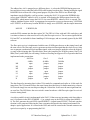
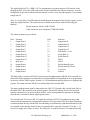
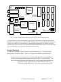
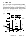
PCI INTERFACE BOARD
This User’s Manual describes the PCI interface board product number ARC-63, Revision 3B, dated
10/25/99. The board is designed to install in a Peripheral Component Interconnect bus that supports
32-bit, 33 MHz operation. A 3.3 volt power source to the board is not required. The board is clasiffied
as a short card, measuring 174.6 mm in length and 106.7 mm in width (4.20 x 6.875 inches), including
the edge connector, which has 124 pads. In the language of the PCI specification, the board receives
commands and parameters from the host computer as a target and writes image and reply data to the
host computer as an initiator, which is analogous to a DMA controller. A Motorola DSP56301 manages the on-board resources and serves as the PCI bus controller. The interface board communicates to
the controller over a fiber optics link. On-board memory consists of a small, fast FIFO memory and a
large, slower DRAM bank, both used for buffering incoming fiber optics data. Additional memory
consists of a boot EEPROM and memory internal to the DSP. Figure 1 shows a block diagram of the
board.
Fiber Rx
Fiber Optic
(50 MHz)
Receiver
8M X 24 bit
DRAM2
8M x 24 bit
DRAM0
Clock
Recovery
8M X 24 bit
DRAM3
PCI Edge
Connector
Clock, Data
Serial-Parallel
Converter
DRAM Controller
DSP56301
1k x 18 bit
FIFO
D0-D17
Port A
4096 x 24 bit
P: RAM
2048 x 24 bit
Fiber Tx
(4 MHz)
Fiber Optic
Transmitter
Ext. Reset
D0-D15, clock
RS-232 Tx, Rx
X:RAM
Misc.
26-pin
33 MHz
Control
AD0-31
2048 x 24 bit
Y:RAM
LEDs
Ext. Sync
Ext. LEDs (2)
ESSI0
PCI Interface
D0-D17
Parity
Connector
Boot EEPROM
8k x 8 bit
OnCE port
Power
ON
Reset
Software
Reset
Fig. 1 - Block diagram of the PCI interface board.
PCI Interface Board, pg. #1
Updated Dec. 2, 1999
Several documents and software packages are provided by Motorola that may be of interest to the user.
These are all available on the DSP website, accessible from www.mot.com. Several of the most useful
documents have been copied here, including the DSP56300 Family Manual (FamilyManual.pdf), the
DSP56301 User’s Manual (UsersManual.pdf), and the PCI application note AN1780 (PCI.pdf). Reference to these manuals will be made in this document.
Circuit Description
The DSP56301 operates at 3.3 volts, whereas the fiber optic parts operate at 5 volts. Toaccomodate the
two voltage requirements a 5 volt to 3.3 volts regulator is installed on the board, and only 5 volt power
is drawn from the edge connector. Several parts the EEPROM, FIFO and DRAM) were chosen in their
low voltage option. Two Cypress CY7C372I PALs operate from both 3.3 and 5 volt supplies and have
inputs that tolerate 5 volts and outputs that reach a maximum of 3.3 volts, providing a simple interface
between 3.3 and 5 volt parts.
The DSP is driven from the 33 MHz PCI bus clock, and employs an internal phase locked loop (PLL)
to multiply the input clock to its internal operating frequency of 78.4 MHz, s described in Section 2.1
of PCI.pdf, as follows PLL_INIT EQU
$750012
MOVEP #PLL_INIT,X:PCTL
; PLL = 33 MHz x 19 / 8 = 78.4 MHz
; Initialize PLL
The DSP boots from a 8k x 8 bit on-board EEPROM (Catalyst part number CAT28LV64P, any speed)
that operates at 3.3 volts. When the DSP RESET* signal makes a low to high transition the input lines
MODD to MODA are set to a 0001 by PAL U23 to cause the DSP to execute an internal program that
reads the DSP program from the EEPROM, and starts executing it from program address zero. The
RESET* line may be asserted low true by the host computer’s assertion of the PCIRST* line if the
jumper JP11 is installed. The Sun Microsystems Ultra 5 used for the interface board development
asserted this signal only during the power-up sequence and correctly released it several seconds prior
to accessing the interface board during the booting process. For host computers whose PCIRST* line
may not be well defined the jumper JP11 should be removed and booting accomplished instead from
a power-on reset circuit that asserts the RESET* line for several hundred milliseconds after the 5 volts
power has been turned on.
All DSP code executes from memory internal to the DSP, which must be loaded with the desired code.
There are three mechanisms for doing this. The boot code written to the EEPROM is generated with a
short script named "rom" that assembles and links a DSP source code file named "pciboot.asm"
written in assembly language with the assembler parameter DOWNLOAD=ROM to generate a
Motorola S-record file named "pci.s" that is loadable into an EEPROM burning machine. The script
"host" sets DOWNLOAD=HOST to generate a file named "pci.lod" that can be downloaded via the
host over the PCI bus to the DSP. The script "once" sets DOWNLOAD=ONCE to generate a file
named "pci.lod" that can be loaded into the DSP with the OnCE in-circuit emulator facility that
Motorola provides. The DSP source code file "pciboot.asm" has several conditional assembly
directives at the beginning to set execution and EEPROM load addresses to certain values depending
on the DOWNLOAD parameter, and to follow the protocol of the three different solftware loading
mechanisms. To summarize -
PCI Interface Board, pg. #2
Updated Dec. 2, 1999
script name
rom
host
once
DOWNLOAD
ROM
HOST
ONCE
Output file
pci.s
pci.lod
pci.lod
Start Adress
P:INIT_PCI
P:START
P:START
Functionality
Program the EEPROM externally
Download via host computer
Load via OnCE emulator
The beginning of the file "pciboot.asm" contains two routines located in an unused portion of the
vectored interrupt table. The first of these, INIT_PCI, initializes the DSP’s PCI controller, and is
executed only when the board boots from EEPROM on power-on. A few seconds after power on the
host computer interrogates the PCI bus to find out what boards are installed and configures this
inteface board. The booting procedure ends with program execution starting at address P:0, where the
EEPROM program inserts a JMP INIT_PCI instruction. INIT_PCI sets the phase lock loop parameter
as described above and does a self-configuration and personal software reset of the PCI controller in
the DSP, as described in Section 2.2 of PCI.pdf. After configuring the PCI controller the DSP program
overwrites the instruction at P:0 with JMP START to skip over the INIT_PCI routine, where the
START address begins configuring the DSP and processing commands. Similarly, the "host" and
"once" options place a JMP START instruction at P:0 to skip over the PCI_INIT routine. Executing
the INIT_PCI routine after the host computer has booted will cause the host computer to crash since
the host computer overwrites the configuration registers with its own values and doesn’t tolerate
foreign values.
The second routine is for downloading the file "pci.lod" generated with the script "host" to the DSP
via the PCI bus of the host computer. This is useful to allow development of interface board software
in the same machine as its being executed, and to download different software versions than are
resident in the ROM. The routine is labeled DOWNLOAD_PCI_DSP_CODE and uses DSP software
that is resident in DSP ROM for loading DSP code over the PCI bus, as described in Appendix A of
the User’s Manual. The PCI interface of the DSP is first placed in a mode where it does not insert PCI
addresses in the data stream (IAE=0, described below) and a sanity word is read from the PCI bus to
establish communication. The Operating Mode Register OMR is then set to $00000C to cause the PCI
loading software to be executed once the program jumps to the program resident in the DSP starting
at location $FF0000. The first two words of the file "pci.lod" contain the number of DSP words to be
loaded and the starting load address, which is also the address where the loading routine jumps to after
it is finished. These two words are set in the "pciboot.asm" file in the assembler directives; the starting
address is set to zero and a jump to the INIT routine is placed there so that the PCI self-configuration
and download DSP software will not be executed. Care should be exercised not to modify the
INIT_PCI and downloading routines when downloading DSP code because an error introduced in
either of them will necessitate the host computer being re-booted so correct software can be loaded
from the EEPROM.
The "once" script allows for the DSP to be loaded from the On Chip Emulator (OnCE) port that
Motorola has incorporated into the DSP. To use this port a Command Converter is connected via a
small ribbon connector to the OnCE connector on the interface board, and another ribbon cable is
connected between the Command Converter and a Motorola-supplied interface board in a Sun, PC or
Mac. These are marketed in the ADS, or Advanced Development System, line of products, and are
described in the Motorola Web site. A program on the computer hosting the ADS can read the
"pci.lod" file produced by the "host" script and load it into the DSP. This is particularly useful if
PCI Interface Board, pg. #3
Updated Dec. 2, 1999
extensive DSP code development is done by the user since the ADS incorporates many useful development tools such as breakpoint insertion, and register, memory and program inspection, program
assembly and disassembly. All the interface board software development was done in this mode.
A software reset button is located on the front panel of the PCI interface board. It does not assert the
hardware RESET* line to the DSP, which is only asserted on power-up, but rather asserts the interrupt
line IRQC* that causes the DSP program to jump to an interrupt service routine that sets the program
counter to the beginning of the program INIT and sets the stack pointer to the top of the stack. This
switch can be used to get out of locked up DSP code without having to reboot the host computer. The
switch on the board is OR’d with two pins from the external 26-pin connector so a switch external to
the host computer can be installed by the user.
Commands and parameters are transmitted to the controller timing board following the protocol
discussed in the timing board User’s Manual. The data words are all 33 bits long, containing a start bit,
a preamble bit (normally $AC, and $53 for resettting the timing board), and 24 bits of data. A fiber
optic transmitter is connected directly to the clock and data output lines of the Extended Synchronous
Serial Interface (ESS1) port 0 of the DSP, described in Chapter 7 of UserManual.pdf. It is
programmed for a clock rate close to 4 MHz and 8-bit per word operation. The XMT_WRD routine
transmits a byte at a time to the serial port data register, building up the start bit, preamble byte, data
bytes and trailing zeroes explicitly in software. It samples the Transmitter Data Register Empty (TDE
bit #6) of the ESSI0 Status Register before writing each byte to the transmitter Data register TX00.
The port is configured by writing to the Control Registers CRA0 and CRB0, where only the two lines
STD0 and SCK0 are configured as serial ports, the rest being used as general purpose I/O ports. The
comments in the source code of "pciboot.asm" that set the CRA0 and CRB0 registers describe the port
configuration.
A bank of dynamic random access memory (DRAM) parts is implemented to buffer images should the
host computer not be able to write images to user memory space fast enough to keep up with image
data from the controller. It consists of a total of nine page mode 8Meg x 8 bit memories grouped into
three memory spaces. Each group has common read, write and column access strobe signals generated
by the DSP, and separate row access enable lines RASn*. A common DRAM control register DCR is
programmed to the maximum time between refresh cycles, page logic enabled, and the appropriate
page size and wait states for the DRAM memory installed, as described in Sections 9.2.2 and 9.6.1 of
Family.Manual.pdf. The memory map to DSP space are controlled by the Address Attribute Register
AAR0, AAR2 and AAR3, and are programmed as follows Date memory Y: $800000 to $FFFFFF asserts DRAM access with AA0/RAS0*
Date memory Y: $000000 to $7FFFFF asserts DRAM access with AA2/RAS2*
Data memory X: $000000 to $7FFFFF asserts DRAM access with AA3/RAS3*
The memory spaces X:$0 to X:$000FFF and Y:$0 to Y:$000FFF are mapped to fast memory internal
to the DSP. These Y: locations are used for buffering images, while the X: space is used for parameter
storage and should not be overwritten with image data. Similarly the memory space at X:$FF0000 and
Y:$FF0000 are reserved and should not be used for image storage.
PCI Interface Board, pg. #4
Updated Dec. 2, 1999
The address line AA1 is mapped to two different places - it selects the EEPROM during power-on
boot and also selects reading the buffer FIFOs after booting has taken place. During booting the signal
ROM/FIFO derived from one of the general purpose I/O pins of the ESSI is in a default high
impedance state held high by a pull up resistor, causing the PAL U14 to assert the EEPROM chip
access signal CEROM* whenever AA1 is asserted. After booting the DSP program clears the line
ROM/FIFO, which instead causes the PAL U14 to assert RDFIFO* whenever AA1 is asserted. The
Address Attribute Register AAR1 is programmed to respond to accesses to data memory Y:$FFF000
to $Y:FFFFFF, so the memory location RFFIFO is simply set to $FFFFFF, and the simple instruction
MOVEP
Y:RDFIFO,X0
reads the FIFO contents into the data register X0. The FIFO is 18 bits wide and 1024 words deep, and
is written to whenever a data word is received by the fiber optic receiver. The two most significant bits
D16 and D17 are included for future handling of 18-bit images, and are currently ignored by the DSP
software.
The fiber optic receiver is implemented with the same 50 MHz parts that are on the timing board, and
the same circuit. The fiber optic receiver generates an electrical data signal that the clock recovery chip
uses to generate synchronized clock and data signals, with seven jumpers needed to select the frequency range of the incoming data. The table below shows the jumpering for 50 MHz systems (Gen II), 40
MHz (Gen I), and 4 MHz (for self testing). Neither self-testing nor support of Gen I operation has been
implemented at the present time.
Self-Test
Gen I
Gen II
4 MHz
40 MHz
50 MHz
M0
open
jumper
jumper
M1
open
jumper
jumper
M2
jumper
jumper
jumper
L0
open
open
jumper
L1
open
jumper
jumper
L2
jumper
jumper
jumper
N
jumper
open
open
The data format for incoming data is either 32-bit mode for commands and replies or 16-bit mode for
image data. The 32-bit mode follows the same format described above for data transmission, whereas
16-bit mode simply has one start bit preceeding the 16 data bits. In all cases the most significant bits
are sent first. The LED below the reset switch is turned on when a valid fiber optic signal is received
from the timing board.
A serial-to-parallel circuit is implemented in the PAL U14 that converts incoming serial data either to
two 16 bit entries in the FIFO (if MODE = 1) or a single entry in the FIFO for image data (MODE =
0). The PAL generates the write FIFO signal WRFIFO*. A signal named FSYNC* for frame synchronization is also generated following the same convention discussed in the timing board manual for
adaptive optics applications. It is routed to the DSP, and could be routed to the external connector on
special user request by re-programming the PAL.
PCI Interface Board, pg. #5
Updated Dec. 2, 1999
The signal labeled AUX1 = SRD0 = PC4 is programmed as a general purpose I/O bit and is wired
through the PAL U14 to the LED on the corner of the board and to the external connector. It can be
manipulated by the user to indicate that data transfer is active, or for any other purpose. It is presently
simply left off.
There is a 26-pin, three row DB connector installed on the front panel of the board to support several
input and output functions. The connectors are available from Newark, with the following part
numbers Board connector, female, AMP 5120262
Cable connector, male, Amphenol 174D026PAA000
The connector pinout is given below Pin #
1
2
3
4
5
6
7
8
9
10
11
12
13
Function
Output Data 1
Output Data 3
Output Data 5
Output Data 7
Output Data 9
Output Data 11
Output Data 13
Output Data 15
Input sync
Output Data 0
Output Data 2
Output Data 4
Output Data 6
Pin #
14
15
16
17
18
19
20
21
22
23
24
25
26
Function
Output Data 8
Output Data 10
Output Data 12
Output Data 14
Data Strobe = AA3
Serial Data Tx
Serial Data Rx
LED 1
LED 2
Switch normally open
Switch normally closed
5 volts out
Ground
The Data Strobe is just the AA3/RAS3* pin also used for addressing the DRAM. IF it is needed as a
data strobe for this application it cannot also be used for DRAM access and needs to be re-programmed
by the user with the AAR3 register. Section 9.6.1 of FamilyManual.pdf describes how to program this
register. The output data lines D0-D15 are buffered data lines from the DSP.
The input synchronization signal is connected to the PAL U23. Presently this is wired in the PAL to
the signal AUX3 that connects to the general purpose I/O pin PC0 and may be used for any input
function. Alternatively, on special request the PAL can be re-programmed to generate an interrupt
when the line is asserted to insure rapid response times.
The Serial Rx and Tx lines are RS-232 signal derived from a SN75155 asynchronous driver chip
connected to the synchronous communication interface (SCI) pins of the DSP. They allow bidirectional communication directly with the DSP for controlling or synchronizing with external hardware. Pads
are included on the interface board for the user to install filter capacitors C44 and C45 on the +/- 12
volt power supply lines if they are noisy. The LED pin 1 is connected to the PAL output pin driving
PCI Interface Board, pg. #6
Updated Dec. 2, 1999
the LED that indicates that the fiber optic receiver line has received a valid signal. The LED pin 2 is
connected through the PAL to the DSP general I/O pin AUX1 = PC4 discussed above. The two pins
for operating a switch can be wired to a remote switch that is more accessible than the one located on
the board for software resetting during development sessions. Finally, +5 volts and ground are made
available for powering any external circuitry that may the user may implement.
PCI interface
The PCI interface of the DSP56301 is described extensively in Chapter 6 of UserManual.pdf, and in
the application note named PCI.pdf. An extensive set of register accessible from the DSP program and
a smaller set of registers accessible from the host computer are used to control its operation. Below are
described some of the implementation details of the supplied DSP program.
Soon after booting the following code is executed to configure the PCI port:
MOVEP
NOP
BSET
BSET
NOP
#$100000,X:DCTR
; HI32 mode = PCI
#MACE,X:DPCR
#IAE,X:DPCR
; Master access counter enable
; Insert PCI address before data
; End of PCI programming
Writing the indicated value to the DSP Control Register DCTR)configures the HI32 port as a PCI
controller. Setting the Master Access Counter Enable MACE bit 18 in the DSP PCI Control Register
(DPCR) enables the burst mode counter so more than one word can be written to the PCI bus after
writing a single address. The Insert Address Enable IAE bit 21 being set causes the PCI address to be
written before the data is written whenever the host computer writes to the DSP, allowing the DSP
software to compute the DSP memory address where to put the data. This permits simple tables to be
memory mapped between the host computer and the DSP.
The PCI interface of the DSP contains a 6 x 24-bit FIFO for receiving data written by the host computer, called the DSP Receive Data FIFO DRXR. The DSP PCI Master control register DPMC has its bits
23-22 cleared on reset which sets the translation mode in transferring 32-bit PCI words to 24-bit DSP
such that each PCI word gets read as two 16-bit DSP words, occupying two locations of the FIFO.
Each word written to the interface board then occupies four of the six locations of the FIFO, two for
the PCI address and two for the data. To ensure that the FIFO does not lose data from being overfilled
the host computer must monitor the TRDY bit 0 in the Host interface Status Register HSTR for a one
to be sure the FIFO is empty before writing to it. The DSP program monitors the Slave Receive Data
Request SRRQ bit 2 of the DSP Status Register DSR to be set, which indicates that the host computer
has written to the receive FIFO and can be read. The following lines of code reads 32 bits of the PCI
word in two passes into the X0 and X1 register, then calls the SQUASH routine to compress it into a
single 24-bit DSP register, losing the eight most significant bits in the process:
JCLR
MOVEP
JCLR
#SRRQ,X:DSR,*
X:DRXR,X0
#SRRQ,X:DSR,*
; Wait for receiver to be not empty
; Get least significant word
PCI Interface Board, pg. #7
Updated Dec. 2, 1999
MOVEP
JSR
X:DRXR,X1
<SQUASH
; Get most significant word
; Convert 2 x 16-bit PCI words in X0 and X1 into one 24-bit DSP word in A1
SQUASH MOVE
X1,A
LSL
#16,A
ADD
X0,A
RTS
The DSP writes words to the PCI bus in a more involved procedure. The 16 least significant bits of the
DSP PCI Master Control Register DPMC contain the 16 most significant bits of the PCI address to be
written to. The bits 23-22 of the DPMC register specify that the DSP Master Transmit Data FIFO
DTXM will write two of its 16-bit data words into one 32-bit PCI word, similar to how the receiver
works. The burst length bits 21-16 are set to zero to write one word per address. The 16 least
significant bits of the DSP PCI Address Register DPAR contain the 16 least significant bits of the PCI
address to be written to. The DPAR bits 23-20 are set low to enable all four bytes, causing 32-bit
words to be written to the PCI bus, while the PCI command in bits 19-16 are set to a 0111 to mean
memory write. The 24-bit data word to be written is loaded 16 bits at a time to the DTXM if the Master
Transmit Request MTRQ bit 1 of the DSP PCI Status register DPSR is set. Once the DPMC and
DTXM register are loaded writing the value to the DPAR register initiates the write cycle onto the PCI
bus, as the DSP makes a PCI bus arbitration request, receives a grant, asserts the desired PCI address
on the multiplexed address/data lines AD31-0, after which the word is asserted on the same signal
lines. Monitoring of the Master Address Request MARQ bit 4 of the DPSR is also done to ensure that
the PCI bus is available for a new transaction. For writing image data the burst mode is enabled by
setting the appropriate bits of the DPMC register, and image data is written as two 16-bit image pixels
in a single 32-bit PCI word.
JCLR
MOVEP
JCLR
MOVEP
#MTRQ,X:DPSR,*
X0,X:DTXM
#MTRQ,X:DPSR,*
X1,X:DTXM
; Make sure the transmitter is not full
; Write least sig. word to transmitter
; Make sure the transmitter is not full
; Write most sig. word to transmitter
JCLR
MOVEP
MOVE
MOVE
OR
JCLR
MOVE
#MARQ,X:DPSR,*
; Wait for completion of PCI transaction
X:REPLY_ADR_MSW,X:DPMC ; Get reply address most sig. word
#$070000,A
X:REPLY_ADR_LSW,X0 ; Get reply address least sig. word
X0,A
#MARQ,X:DPSR,*
; Wait for completion of PCI transaction
A,X:DPAR
; Write word to PCI bus
The DSP mask number (3F48S) currently available From Motorola does not calculate parity correctly,
necessitating external circuitry to calculate it and insert it onto the bus when needed. A bank of four
9-bit parity chips sample the 32 multiplexed address/data lines AD00-AD31 and the four command
bits C0-C3 and connect the results to the parity PAL U23 to calculate a net parity. The address parity
PCI Interface Board, pg. #8
Updated Dec. 2, 1999
FO Test Points
PAL U14
PCI Reset
Fiber Optic Rx
FO Speed
24M x 24 bit DRAM
Serial-toParallel
Fiber Optic Tx
EEPROM
8k x 8 bit
Reset
OnCE
FO OK
Test Points
PAL U23
DSP56301
Parity
+3V Gnd +5V
External 26-pin
Connector
ARC-63
1
2
ASTRONOMICAL RESEARCH CAMERAS, INC.
PCI INTERFACE BOARD REV. 3B 10/25/99
Parity Select
Fig. 2 - Layout of the principal components of Rev. 3B of the PCI interface board.
is asserted on the PCI line PAR during the address phase if the interface board is the bus master as
determined by sampling the bus grant line GNT*. The data parity is asserted during the data phase if
a write cycle is underway, as determined by examining the command line C0, whether or not the
interface board is the bus master or not. Motorola has promised that future mask revisions of this DSP
will correct this flaw, but for now this workaround seems to work.
Jumper Summary
The principal components of the PCI interface board are shown in Fig. 2. The default jumper
placements are shown in the figure. Three sets of jumpers select different operating modes FO Speed selects the frequency range of incoming fiber optic data, as described above.
PCI Reset with a jumper installed connects the signal PCIRST* to the DSP RESET* line.
Parity Select when installed to the left between pins 1 and 2 connects the on-board parity
generation circuitry to the PCI parity line PAR. When the jumper is
installed to the right between pins 2 and 3 PAR is generated by the DSP.
PCI Interface Board, pg. #9
Updated Dec. 2, 1999