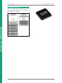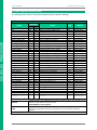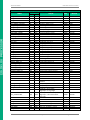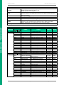
1
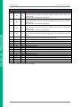
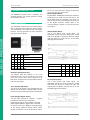
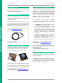
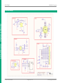
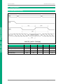
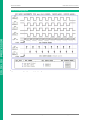
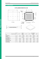
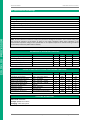
4D
SYSTEMS
TURNING TECHNOLOGY INTO ART
DATASHEET
GOLDELOX Processor
Embedded Graphics Processor
Document Date: 6th September 2012
Document Revision: 1.0
Uncontrolled Copy when printed or downloaded.
Please refer to the 4D Systems website for the latest Revision of this document
GOLDELOX PROCESSOR
Contents
1. Description...................................................................................................................................3
2. Features .......................................................................................................................................3
3. Applications .................................................................................................................................4
4. Pin Configuration and Summary ..................................................................................................5
5. Hardware Interface - Pins.............................................................................................................7
5.1. Display Interface .................................................................................................................................... 7
5.2. SPI Interface – Master Mode Only ......................................................................................................... 8
5.3. Serial Port - UART ................................................................................................................................... 8
5.4. General Purpose I/O Interface ............................................................................................................... 8
5.5. System Pins .......................................................................................................................................... 10
6. 4DGL - Software Language .........................................................................................................11
7. In Circuit Serial Programming ICSP .............................................................................................11
8. Memory Organisation ................................................................................................................12
9. System Registers Memory Map .................................................................................................13
10. Hardware Tools ........................................................................................................................16
10.1. 4D Programming Cable ...................................................................................................................... 16
10.2. Evaluation Display Modules ............................................................................................................... 16
11. 4D Systems - Workshop 4 IDE ..................................................................................................16
11.1. Workshop 4 – Designer Environment ................................................................................................ 16
11.2. Workshop 4 – ViSi Environment......................................................................................................... 17
11.3. Workshop 4 – Serial Environment...................................................................................................... 17
12. Reference Design .....................................................................................................................18
13. Timing Diagrams ......................................................................................................................19
13.1. Display Write Data Timing.................................................................................................................. 19
13.2. Display Read Data Timing ................................................................................................................... 20
13.3. SPI Timing Diagram ............................................................................................................................ 21
14. Package Details ........................................................................................................................22
15. PCB Land Pattern......................................................................................................................23
16. Specifications and Ratings........................................................................................................24
17. Legal Notice..............................................................................................................................25
18. Contact Information .................................................................................................................25
GOLDELOX PROCESSOR
4D SYSTEMS
GOLDELOX Processor
1. Description
2. Features
The GOLDELOX is a custom embedded graphics
controller designed to interface with many popular
OLED and LCD display panels. Powerful graphics,
text, image, animation and countless more
features are built right inside the chip. It offers a
simple plug-n-play interface to many 8bit 80-Series
colour LCD and OLED displays.
The chip is designed to work with minimal design
effort and all of the data and control signals are
provided by the chip to interface directly to the
display. Simply choose your display and interface it
to the GOLDELOX on your application board. This
offers enormous advantage to the designer in
development time and cost saving and takes away
all of the burden of low level design.
The GOLDELOX belongs to a family of processors
powered by a highly optimised soft core virtual
engine, EVE (Extensible Virtual Engine). EVE is a
proprietary, high performance virtual processor
with an extensive byte-code instruction set
optimised to execute compiled 4DGL programs.
4DGL (4D Graphics Language) was specifically
developed from ground up for the EVE engine
core. It is a high level language which is easy to
learn and simple to understand yet powerful
enough to tackle many embedded graphics
applications.
The device offers modest but comprehensive I/O
features and can interface to SPI, serial, analogue,
digital, buttons, joystick and Dallas 1-wire devices.
Provision is also made for creating complex sound
effects for audible user feedback with an extended
RTTTL tone generator.
All of the display built-in driver libraries implement
and share the same high-level function interface.
This allows your GUI application to be portable to
different display controller types.
4D Systems software development IDE called
Workshop 4 is FREE and there are no licensing
requirements.
The GOLDELOX offers one of the most flexible
embedded graphics solutions available.
© 2012 4D SYSTEMS
• Low-cost OLED, LCD and TFT display graphics
user interface solution.
• Ideal as a standalone embedded graphics
processor or interface to any host controller as a
graphics co-processor.
• Connect to any colour display that supports an
80-Series 8 bit wide CPU interface. All data and
control signals are provided.
• Built in high performance virtual processor
engine (EVE) with an extensive byte-code
instruction set optimised for 4DGL, the high
level 4D Graphics Language.
• 2 x GPIO ports supports:
• Digital I/O
• A/D converter with 8/10 bit resolution
• Complex sound generation
• Dedicated RTTTL tune engine
• Multi-Switch Joystick
• Dallas 1-Wire
• 10KB of Flash memory for user code storage
and 510 bytes (255 x 16bit vars) of RAM for user
variables.
• 1 x 32bit free running system timer with 1msec
resolution.
• 4 x 16bit user timers with 1msec resolution
• Asynchronous hardware Serial port with autobaud feature (300 to 256K baud).
• Hardware SPI port interface for micro-SD/microSDHC memory cards or Serial Flash memory
chips for storing of icons, images, animations,
etc.
• Comprehensive set of built in high level 4DGL
graphics functions and algorithms that can draw
lines, circles, text, and much more.
• Display full colour images, animations, icons and
video clips.
• 8x8 built-in system font and support for
unlimited user customisable fonts with fixed or
proportional spacing with the aid of a freely
provided Font-Tool.
• Single 3.3 Volt Supply @12mA typical.
• Available in a tiny 6mm x 6mm 28pin QFN.
Page 3 of 25
www.4dsystems.com.au
GOLDELOX PROCESSOR
4D SYSTEMS
GOLDELOX Processor
3. Applications
• Industrial (general).
• Test, measurement
instrumentation
and
general
purpose
• Elevator Control Systems.
• Point of Sale Terminals.
• Home Appliances (general).
• Security Systems.
• Access Control Systems.
• Air-conditioning Control Systems.
• Universal Remote Control.
• Automotive (general).
• Electronic Gauges and Meters.
• Portable ECG Systems.
• Portable Blood Pressure Monitors.
• Aviation (general).
• Gaming and Slot Machines.
• And much more..
© 2012 4D SYSTEMS
Page 4 of 25
www.4dsystems.com.au
GOLDELOX PROCESSOR
4D SYSTEMS
GOLDELOX Processor
4. Pin Configuration and Summary
Pin
Symbol
I/O
1
RD
O
2
WR
O
3
REF
P
4
RS
O
5
6
7
GND
CLK1
CLK2
P
I
O
8
SDCS
O
9
CS
O
10
RES
O
GOLDELOX Processor Pin Out
Description
Display Read strobe signal. GOLDELOX asserts this signal LOW when reading data
from the display. Connect this pin to the Read (RD) signal of the display.
Display Write strobe signal. GOLDELOX asserts this signal LOW when writing data
to the display. Connect this pin to the Write (WR) signal of the display.
Internal voltage regulator filter capacitor. Connect a 4.7uF to 10uF capacitor
from this pin to Ground.
Display Register Select.
LOW: Display index or status register is selected.
HIGH: Display GRAM or register data is selected.
Connect this pin to the Register Select (RS or A0 or C/D or similar naming
convention) signal of the display.
Ground.
System Clock input 1 of a 12MHz crystal.
System Clock input 2 of a 12MHz crystal.
SPI device Chip Select. Connect this pin to the Chip Enable (CE or CS) signal of the
external SPI device (SD/SDHC memory card, Serial Flash chip, etc.).
Display Chip Select. GOLDELOX asserts this signal LOW when accessing the
display. Connect this pin to the Chip Select (CS) signal of the display.
Display RESET. GOLDELOX initialises the display by strobing this pin LOW.
Connect this pin to the Reset (RES) signal of the display.
I = Input, O = Output, P = Power, A = Analogue
© 2012 4D SYSTEMS
Page 5 of 25
www.4dsystems.com.au
GOLDELOX PROCESSOR
4D SYSTEMS
GOLDELOX Processor
Pin
Symbol
I/O
11
SCK
O
12
SDI
I
13
SDO
O
14
TX0
O
15
RX0
I
16
17
18
19
20
21
22
23
24
25
26
27
28
PAD
GND
VCC
D0
D1
D2
D3
D4
D5
D6
D7
RESET
IO1
IO2
GND
P
P
I/O
I/O
I/O
I/O
I/O
I/O
I/O
I/O
I
I/O/A
I/O
P
GOLDELOX Processor Pin Out (continued…)
Description
SPI Serial Clock output. Connect this pin to the SPI Serial Clock (SCK) signal of the
external device. Nominally reserved for SD/SDHC memory card or serial flash
memory chip.
See Section 8.3 for detailed timing diagram.
SPI Serial Data Input. Connect this pin to the SPI Serial Data Out (SDO) signal of
the external device. Nominally reserved for SD/SDHC memory card or serial flash
memory chip.
See Section 8.3 for detailed timing diagram.
SPI Serial Data Output. Connect this pin to the SPI Serial Data In (SDI) signal of the
external device. Nominally reserved for SD/SDHC memory card or serial flash
memory chip.
See Section 8.3 for detailed timing diagram.
Asynchronous Serial Transmit pin. Output data is at TTL voltage levels. Connect
this pin to external device Serial Receive (Rx) signal. This pin is tolerant up to 5.0V
levels.
Asynchronous Serial Receive pin. Connect this pin to external device Serial
Transmit (Tx) signal. This pin is tolerant up to 5.0V levels.
Ground.
Positive supply with respect to GND pin.
Display Data Bus bit 0.
Display Data Bus bit 1.
Display Data Bus bit 2.
Display Data Bus bit 3.
Display Data Bus bit 4.
Display Data Bus bit 5.
Display Data Bus bit 6.
Display Data Bus bit 7.
Master Reset signal. Connect a 4.7K resistor from this pin to VCC.
General purpose IO1 pin. See Section 2.4 for more detail.
General purpose IO2 pin. See Section 2.4 for more detail.
Exposed metal pad under the package, must connect to GND.
I = Input, O = Output, P = Power, A = Analogue
© 2012 4D SYSTEMS
Page 6 of 25
www.4dsystems.com.au
GOLDELOX PROCESSOR
4D SYSTEMS
GOLDELOX Processor
5. Hardware Interface - Pins
The GOLDELOX provides both a hardware and
software interface. This section describes in detail
the hardware interface.
5.1. Display Interface
The GOLDELOX supports LCD and OLED displays
with an 80-Series 8 bit wide CPU data interface.
The connectivity to the display is easy and straight
forward. The chip generates all of the necessary
timing to drive the display.
Be sure to check with your display manufacturer
for the correct name and function.
RES pin (Display Reset):
Display RESET. GOLDELOX initialises the display by
strobing this pin LOW. Connect this pin to the
Reset (RES) signal of the display. This signal can
also be used to control the back-light of the LCD or
as the DC/DC converter enable. Refer to the
reference design in Section 7 in this document for
an example.
WR pin (Display Write):
This is the display write strobe signal. The
GOLDELOX asserts this signal LOW when writing
data to the display in conjunction with the display
data bus (D0-D7). Connect this pin to the Write
(WR) signal of the display.
CS
RS
RD WR Operation
0
0
0
1
Read Display Status Register
0
0
1
0
Write Display Index Register
0
1
0
1
Read Display GRAM Data
0
1
1
0
Write Register or GRAM Data
Item
1
X
X
X
No Operation
Display Operation Table
D0-D7 pins (Display Data Bus):
The Display Data Bus (D0-D7) is an 8 bit
bidirectional port and all data writes and reads
occur over this bus. Other control signals such as
RW, RD CS, and RS synchronise the data transfer to
and from the display.
CS pin (Display Chip Select):
The access to the display is only possible when the
Display Chip Select (CS) is asserted LOW. Connect
this pin to the Chip Select (CS) signal of the display.
Sym
Min
Typ Max Unit
Write Low Pulse
tWL
170
-
-
ns
Write High Pulse
tWH
85
-
-
ns
Write Bus Cycle Total
tWT
255
-
-
ns
Write Data Setup
tDS
85
-
-
ns
RD pin (Display Read):
This is the display read strobe signal. The
GOLDELOX asserts this signal LOW when reading
data from the display in conjunction with the
display data bus (D0-D7). Connect this pin to the
Read (RD) signal of the display.
RS pin (Display Register Select):
The RS signal determines whether a register
command or data is sent to the display.
LOW: Display index or status register is selected.
HIGH: Display GRAM or register data is selected.
Connect this pin to the Register Select (RS) signal
of the display. Different displays utilise various
naming conventions such as RS, A0, C/D or similar.
© 2012 4D SYSTEMS
Page 7 of 25
www.4dsystems.com.au
GOLDELOX PROCESSOR
4D SYSTEMS
GOLDELOX Processor
Item
Sym
Min
Typ
Max
Unit
Read Low Pulse
tRL
300
-
-
ns
Read High Pulse
tRH
300
-
-
ns
Read Bus Cycle Total
tRT
600
-
-
ns
Read Data Hold
tDH
150
-
-
ns
5.2. SPI Interface – Master Mode Only
The GOLDELOX supports micro-SD/micro-SDHC
memory cards as well as Serial Flash memory chips
via its hardware SPI interface. These storage
devices are used for all multimedia file storage
such as images, animations and movie clips. The
memory card can also be used as general purpose
storage for data logging applications. Support is
available for micro-SD with up to 2GB capacity and
for high capacity HC memory cards starting from
4GB and above. The GOLDELOX also supports any
other general purpose SPI serial device.
This is referred to as the COM0 module. The
primary features are:
• Full-Duplex 8 bit data transmission and
reception through the TX and RX pins.
• Data format: 8 bits, No Parity, 1 Stop bit.
• Auto Baud feature.
• Baud rates from 300 baud up to 256K baud.
• Single byte transmits and receives or a fully
buffered service. The buffered service
feature runs in the background capturing
and buffering serial data without the user
application having to constantly poll the
serial port. This frees up the application to
service other tasks.
The Serial port is also the primary interface for
downloading user application code (compiled
4DGL byte-code) into the GOLDELOX flash
program memory. Once the download is complete
the serial port is available for user application.
Note: Low level PmmC chip programming and
updates also take place via the serial port.
Refer to “Section 4. In-Circuit-Serial-Programming
(ICSP)” for further details.
SDI pin (SPI Serial Data In):
The SPI Serial Data Input (SDI). It connects to the
Serial Data Out (SDO) pin of external SPI device.
SDO pin (SPI Serial Data Out):
The SPI Serial Data Output (SDO). This pin connects
to the Serial Data In (SDI) signal of the external SPI
device.
SCK pin (SPI Serial Clock):
The SPI Serial Clock output (SCK). This pin connects
to the Serial Clock (SCK) signal of the external SPI
device.
SDCS pin (SPI Chip Select):
SPI device Chip Select (SDCS). Connect this pin to
the Chip Enable (CE or CS) signal of the external SPI
device.
Also refer to “Section 13.3 SPI Timing Diagram”
TX pin (Serial Transmit):
Asynchronous Serial port Transmit pin, TX.
Connect this pin to external serial device Serial
Receive (Rx) signal.
RX pin (Serial Receive):
Asynchronous Serial port Receive pin, RX. Connect
this pin to external serial device Serial Transmit
(Tx) signal.
5.4. General Purpose I/O Interface
There are 2 GPIO pins available, IO1 and IO2. Each
GPIO has a multitude of high level functions
associated with it and these can be selected within
4DGL user application code.
Refer to the separate document titled
“GOLDELOX-Internal-Functions.pdf”
for
a
complete set of built in 4DGL library functions.
IO1, IO2 pins (General Purpose Input Output):
General purpose IO1, IO2 pins. The table below
lists the available GPIO functions and features.
5.3. Serial Port - UART
The GOLDELOX has a dedicated hardware UART
that can communicate with external serial devices.
© 2012 4D SYSTEMS
Page 8 of 25
www.4dsystems.com.au
GOLDELOX PROCESSOR
4D SYSTEMS
GOLDELOX Processor
GPIO Functions and Features
Function
IO1
IO2
Digital Input
√
√
Digital Output
√
√
A/D Converter 8/10 bits
√
--
Dallas 1-Wire support
√
√
Sound Generation, RTTTL Tunes
√
√
Joystick – 5 position multi-switch
√
--
Input/Output:
Both IO1 and IO2 pins can be programmed to be
Inputs or Outputs. Diagram below shows a LED
connected to IO1 (programmed as an output) and
a button connected to IO2 (programmed as an
input).
Joystick - Multi Switch:
Multiple buttons or a multi-switch Joystick can be
connected to the IO1 pin. Up to 5 buttons or a 5
position multi-switch joystick connects to a
junction of a resistor ladder network that forms a
voltage divider. The A/D converter of the IO1 pin
internally reads the analogue value and decodes it
accordingly. This feature is supported by dedicated
4DGL library functions. The following diagrams
indicate how to connect up to 5 individual buttons
or a multi-switch joystick to the IO1 pin.
Analogue to Digital Converter:
The IO1 pin can be programmed as an A/D input.
Option is available to select 8 bit or 10 bit
resolution. Diagram below is a circuit of a Light
Dependant Resistor (LDR) connected to IO1 to
measure and record changes in ambient light.
Dallas 1-Wire:
The Dallas 1-Wire protocol is a form of serial
communications designed to operate over a single
data line plus ground reference. Multiple 1-Wire
devices can be attached to the same shared data
line to network many devices. One wire device
support is available on both the IO1 and the IO2
pins.
The diagram below depicts a typical 1-Wire
temperature sensor interface.
© 2012 4D SYSTEMS
Unused buttons do not need resistors to be
connected to the circuit. The table below lists the
buttons and corresponding resistor values.
Page 9 of 25
www.4dsystems.com.au
GOLDELOX PROCESSOR
4D SYSTEMS
GOLDELOX Processor
Number of
Buttons
Button Number
Resistor Value
1
SW1
22K
2
SW2
10K
3
SW3
4.7K
4
SW4
2.2K
5
SW5
1.2K
Sound Output:
The GOLDELOX is capable of generating complex
sounds and RTTTL tunes from its IO1 and IO2 pins.
A simple speaker circuit as shown below can be
utilised.
5.5. System Pins
VCC pin (Device Supply Voltage):
Device supply voltage pin. This pin must be
connected to a regulated supply voltage in the
range of 3.0 Volts to 3.6 Volts DC. Nominal
operating voltage is 3.3 Volts.
GND, PAD pins (Device Ground):
Device ground pins. These pins must be connected
to ground.
RESET pin (Device Master Reset):
Device Master Reset pin. An active low pulse of
greater than 2 micro-seconds will reset the device.
Connect a resistor (1K through to 10K, nominal
4.7K) from this pin to VCC. Only use open collector
type circuits to reset the device if an external reset
is required. This pin is not driven low by any
internal conditions.
CLK1, CLK2 pins (Device Oscillator Inputs):
CLK1 and CLK2 are the device oscillator pins.
Connect a 12MHz AT strip cut crystal with 22pF
capacitors from each pin to GND as shown in the
diagram below.
© 2012 4D SYSTEMS
Page 10 of 25
www.4dsystems.com.au
GOLDELOX PROCESSOR
4D SYSTEMS
GOLDELOX Processor
6. 4DGL - Software Language
7. In Circuit Serial Programming ICSP
The GOLDELOX graphics processor belongs to a
family of processors powered by a highly
optimised soft core virtual engine, EVE (Extensible
Virtual Engine).
The GOLDELOX processor can be re-programmed
with the latest PmmC configuration for updates
and future proofing. The chip-level configuration is
available as a PmmC (Personality-module-microCode) file and the programming must be
performed over the serial interface. The chipresident internal 4DGL functions are part of the
GOLDELOX PmmC configuration file so please
check regularly for the latest updates and
enhancements.
EVE is a proprietary, high performance virtualmachine with an extensive byte-code instruction
set optimised to execute compiled 4DGL
programs. 4DGL (4D Graphics Language) was
specifically developed from ground up for the EVE
engine core. It is a high level language which is
easy to learn and simple to understand yet
powerful enough to tackle many embedded
graphics applications.
4DGL is a graphics oriented language allowing
rapid application development, and the syntax
structure was designed using elements of popular
languages such as C, Basic, Pascal and others.
Programmers familiar with these languages will
feel right at home with 4DGL. It includes many
familiar instructions such as IF..ELSE..ENDIF,
WHILE..WEND, REPEAT..UNTIL, GOSUB..ENDSUB,
GOTO, PRINT as well as some specialised
instructions
SERIN,
SEROUT,
GFX_LINE,
GFX_CIRCLE and many more.
For detailed information pertaining to the 4DGL
language, please refer to the following documents:
“4DGL-Programmers-Reference-Manual.pdf”
“GOLDELOX-4DGL-Internal-Functions.pdf”
To assist with the development of 4DGL
applications, the Workshop 4 IDE combines a fullfeatured editor, a compiler, a linker and a
downloader into a single PC-based application. It's
all you need to code, test and run your
applications.
A PmmC file can only be programmed into the
device via its serial port and an access to this must
be provided for on the target application board.
This is referred to as In Circuit Serial Programming
(ICSP). Diagram below provides a typical
implementation for the ICSP interface.
ICSP Interface
The PmmC file is programmed into the device with
the aid of Workshop 4, the 4D Systems IDE
software (See Section 11). To provide a link
between the PC and the ICSP interface, a specific
4D Programming Cable is required and is available
from 4D Systems.
Using a non-4D programming interface could
damage your display, and void your Warranty.
Note: The GOLDELOX chip is shipped blank and it
must be programmed with the PmmC
configuration file.
© 2012 4D SYSTEMS
Page 11 of 25
www.4dsystems.com.au
4D SYSTEMS
GOLDELOX Processor
8. Memory Organisation
GOLDELOX PROCESSOR
The figure below illustrates how the GOLDELOX
internal memory is organised.
© 2012 4D SYSTEMS
Page 12 of 25
www.4dsystems.com.au
GOLDELOX PROCESSOR
4D SYSTEMS
GOLDELOX Processor
9. System Registers Memory Map
The following tables outline in detail the GOLDELOX system registers and flags.
LABEL
VX1
VY1
VX2
VY2
SYS_X_MAX
SYS_Y_MAX
WRITE_GRAM_REG
READ_GRAM_REG
IMAGE_WIDTH
IMAGE_HEIGHT
IMAGE_DELAY
IMAGE_MODE
CLIP_LEFT_POS
CLIP_TOP_POS
CLIP_RIGHT_POS
CLIP_BOTTOM_POS
CLIP_LEFT
CLIP_TOP
CLIP_RIGHT
CLIP_BOTTOM
FONT_TYPE
FONT_MAX
FONT_OFFSET
FONT_WIDTH
FONT_HEIGHT
TEXT_XMAG
TEXT_YMAG
TEXT_MARGIN
TEXT_DELAY
TEXT_X_GAP
TEXT_Y_GAP
GFX_XMAX
GFX_YMAX
GFX_SCREENMODE
reserved
*NOTES:
Table 5.1: System (BYTE Size) Registers Memory Map
ADDRESS
USAGE
SIZE
DEC HEX
128
129
130
131
132
133
134
135
136
137
138
139
140
141
142
143
144
145
146
147
148
149
150
151
152
153
154
155
156
157
158
159
160
161
162165
0x80
0x81
0x82
0x83
0x84
0x85
0x86
0x87
0x88
0x89
0x8A
0x8B
0x8C
0x8D
0x8E
0x8F
0x90
0x91
0x92
0x93
0x94
0x95
0x96
0x97
0x98
0x99
0x9A
0x9B
0x9C
0x9D
0x9E
0x9F
0xA0
0xA1
0xA20xA5
*NOTES
display hardware GRAM x1 pos
display hardware GRAM y1 pos
display hardware GRAM x2 pos
display hardware GRAM y2 pos
display hardware X res-1
display hardware Y res-1
display GRAM write address
display GRAM read address
loaded image/animation width
loaded image/animation height
frame delay (if animation)
image/animation colour mode
left clipping point setting
top clipping point setting
right clipping point setting
bottom clipping point setting
left clipping point active
top clipping point active
right clipping point active
bottom clipping point active
0 = fixed, 1 = proportional
number of chars in font set
ASCII offset (usually 0x20)
width of font (pixel units)
height of font (pixel units)
text width magnification
text height magnification
text place holder for CR
text delay effect (0-255msec)
X pixel gap between chars
Y pixel gap between chars
width of current orientation
height of current orientation
Current screen mode (0-3)
BYTE
BYTE
BYTE
BYTE
BYTE
BYTE
BYTE
BYTE
BYTE
BYTE
BYTE
BYTE
BYTE
BYTE
BYTE
BYTE
BYTE
BYTE
BYTE
BYTE
BYTE
BYTE
BYTE
BYTE
BYTE
BYTE
BYTE
BYTE
BYTE
BYTE
BYTE
BYTE
BYTE
BYTE
SYSTEM (R/O)
SYSTEM (R/O)
SYSTEM (R/O)
SYSTEM (R/O)
SYSTEM (R/O)
SYSTEM (R/O)
SYSTEM (R/O)
SYSTEM (R/O)
SYSTEM (R/O)
SYSTEM (R/O)
USER
SYSTEM (R/O)
USER
USER
USER
USER
USER
USER
USER
USER
SYSTEM (R/O)
SYSTEM (R/O)
SYSTEM (R/O)
SYSTEM (R/O)
SYSTEM (R/O)
USER
USER
SYSTEM (R/O)
USER
USER
USER
SYSTEM (R/O)
SYSTEM (R/O)
SYSTEM (R/O)
reserved
BYTE
SYSTEM (R/O)
SYSTEM registers are maintained by internal system functions and should not be
written to. They should only ever be read.
DO NOT WRITE to these registers.
USER registers are read/write (R/W) registers used to alter the system behaviour.
USER
Refer to the individual functions for information on the interaction with these
registers.
These registers are accessible with peekB and pokeB functions.
SYSTEM
© 2012 4D SYSTEMS
Page 13 of 25
www.4dsystems.com.au
GOLDELOX PROCESSOR
4D SYSTEMS
LABEL
GOLDELOX Processor
Table 5.2: System (WORD size) Registers Memory Map
ADDRESS
USAGE
SIZE
DEC HEX
SYS_OVERFLOW
SYS_COLOUR
SYS_RETVAL
GFX_BACK_COLOUR
GFX_OBJECT_COLOUR
GFX_TEXT_COLOUR
GFX_TEXT_BGCOLOUR
GFX_OUTLINE_COLOUR
GFX_LINE_PATTERN
IMG_PIXEL_COUNT
IMG_FRAME_COUNT
MEDIA_HEAD
SYS_OUTSTREAM
GFX_LEFT
GFX_TOP
GFX_RIGHT
GFX_BOTTOM
GFX_X1
GFX_Y1
GFX_X2
GFX_Y2
GFX_X_ORG
GFX_Y_ORG
RANDOM_LO
RANDOM_HI
MEDIA_ADDR_LO
MEDIA_ADDR_HI
SECTOR_ADDR_LO
SECTOR_ADDR_HI
SYSTEM_TIMER_LO
SYSTEM_TIMER_HI
TIMER0
TIMER1
TIMER2
TIMER3
83
84
85
86
87
88
89
90
91
92
93
94
95
96
97
98
99
100
101
102
103
104
105
106
107
108
109
110
111
112
113
114
115
116
117
0x53
0x54
0x55
0x56
0x57
0x58
0x59
0x5A
0x5B
0x5C
0x5D
0x5E
0x5F
0x60
0x61
0x62
0x63
0x64
0x65
0x66
0x67
0x68
0x69
0x6A
0x6B
0x6C
0x6D
0x6E
0x6F
0x70
0x71
0x72
0x73
0x74
0x75
INCVAL
118
0x76
TEMP_MEDIA_ADDRLO
TEMP_MEDIA_ADDRHI
GFX_TRANSPARENTCOLOUR
119
120
121
0x77
0x78
0x79
GFX_STRINGMETRIX
122
0x7A
GFX_TEMPSTORE1
123
0x7B
reserved
reserved
SYS_FLAGS1
SYS_FLAGS2
USR_SP
USR_MEM
SYS_STACK
124
125
126
127
128
129
384
0x7C
0x7D
0x7E
0x7F
0x80
0x81
0x180
© 2012 4D SYSTEMS
16bit overflow register
internal variable for colour
return value of last function
screen background colour
graphics object colour
text foreground colour
text background colour
circle/rectangle outline
line draw tessellation
count of pixels in image
count of frames in animation
media sector head position
Output stream handle
image left real point
image top real point
image right real point
image bottom real point
image left clipped point
image top clipped point
image right clipped point
image bottom clipped point
current X origin
current Y origin
random generator LO word
random generator HI word
media byte address LO
media byte address HI
media sector address LO
media sector address HI
1msec system timer LO word
1msec system timer HI word
1msec user timer 0
1msec user timer 1
1msec user timer 2
1msec user timer 3
predec/preinc/postdec/postinc
addend
temporary media address LO
temporary media address HI
Image transparency colour
Low byte = string width
High byte = string height
Low byte = last character printed
High byte = video frame timer
over-ride
reserved
reserved
system control flags word 0
system control flags word 1
User defined stack pointer
255 user variables / array(s)
128 level EVE machine stack
Page 14 of 25
*NOTES
WORD
WORD
WORD
WORD
WORD
WORD
WORD
WORD
WORD
WORD
WORD
WORD
WORD
WORD
WORD
WORD
WORD
WORD
WORD
WORD
WORD
WORD
WORD
WORD
WORD
WORD
WORD
WORD
WORD
WORD
WORD
WORD
WORD
WORD
WORD
USER
SYSTEM
SYSTEM
USER
USER
USER
USER
USER
USER
SYSTEM
SYSTEM
SYSTEM
SYSTEM
SYSTEM
SYSTEM
SYSTEM
SYSTEM
SYSTEM
SYSTEM
SYSTEM
SYSTEM
USER
USER
SYSTEM
SYSTEM
SYSTEM
SYSTEM
SYSTEM
SYSTEM
USER
USER
USER
USER
USER
USER
WORD
USER
WORD
WORD
WORD
SYSTEM
SYSTEM
USER
WORD
SYSTEM
WORD
SYSTEM
WORD
WORD
WORD
WORD
WORD
WORD
WORD
SYSTEM
SYSTEM
FLAGS
FLAGS
USERSTACK
MEMORY
SYSTEMSTACK
www.4dsystems.com.au
GOLDELOX PROCESSOR
4D SYSTEMS
GOLDELOX Processor
*NOTES:
SYSTEM registers are maintained by internal system functions and should not be
written to. They should only ever be read.
DO NOT WRITE to these registers.
USER registers are read/write (R/W) registers used to alter the system
USER
behaviour. Refer to the individual functions for information on the interaction
with these registers.
USERSTACK
Used by the debugging and system extension utilities
MEMORY
255 word size variables for users program
STACK
128 word EVE system stack (STACK grows upwards)
FLAGS are a mixture of bits that are either maintained by internal system
FLAGS
functions or set / cleared by various system functions. Refer to the FLAGS
Register Bit Map table, and individual functions for further details.
These registers are accessible with peekW and pokeW functions.
SYSTEM
REGISTER
SYS_FLAGS1
SYS_FLAGS2
ADDRESS
DEC HEX
Table 5.3: FLAG Registers Bit Map
NAME
126
0x7E
Bit 0
Bit 1
Bit 2
Bit 3
Bit 4
Bit 5
Bit 6
Bit 7
Bit 8
Bit 9
Bit 10
Bit 11
Bit 12
Bit 13
Bit 14
Bit 15
127
0x7F
_STREAMLOCK
_PENSIZE
_OPACITY
_OUTLINED
_BOLD
_ITALIC
_INVERSE
_UNDERLINED
_CLIPPING
_STRMODE
_SERMODE
_TXTMODE
_MEDIAMODE
_PATTERNED
_COLOUR8
_MEDIAFONT
Bit 0
_MEDIA_INSTALLED
Bit 1
Bit 2
Bit 3
Bit 4
Bit 5
Bit 6
Bit 7
Bit 8
Bit 9
Bit 10
Bit 11
Bit 12
Bit 13
Bit 14
Bit 15
_MEDIA_TYPE
_MEDIA_READ
_MEDIA_WRITE
_OW_PIN
_PTR_TYPE
_TEMP1
_TEMP2
_RUNMODE
_SIGNED
_RUNFLAG
_SINGLESTEP
_COMMINT
_DUMMY16
_DISP16
_PROPFONT
© 2012 4D SYSTEMS
USAGE
*NOTES
VALUE
* denotes auto reset
Used internally
Object, 0 = solid, 1 = outline
Text, 0 = transparent, 1 = opaque
box/circle outline 0 = off, 1 = on
* text, 0 = normal, 1 = bold
* Text, 0 = normal, 1 = italic
* Text, 0 = normal, 1 = inverse
* Text, 0 = normal, 1 = underlined
0 = clipping off, 1 = clipping on
Used internally
Used internally
Used internally
Used internally
Used internally
Display mode, 0 = 16bit, 1 = 8bit
0 = internal font, 1 = media font
SYSTEM
SYSTEM
SYSTEM
SYSTEM
SYSTEM
SYSTEM
SYSTEM
SYSTEM
SYSTEM
SYSTEM
SYSTEM
SYSTEM
SYSTEM
SYSTEM
SYSTEM
SYSTEM
0x0001
0x0002
0x0004
0x0008
0x0010
0x0020
0x0040
0x0080
0x0100
0x0200
0x0400
0x0800
0x1000
0x2000
0x4000
0x8000
SYSTEM
0x0001
SYSTEM
SYSTEM
SYSTEM
SYSTEM
SYSTEM
SYSTEM
SYSTEM
SYSTEM
SYSTEM
SYSTEM
SYSTEM
SYSTEM
SYSTEM
SYSTEM
SYSTEM
0x0002
0x0004
0x0008
0x0010
0x0020
0x0040
0x0080
0x0100
0x0200
0x0400
0x0800
0x1000
0x2000
0x4000
0x8000
SD or FLASH device is
detected/active
0 = SD, 1 = FLASH chip
1 = MEDIA read in progress
1 = MEDIA write in progress
0 = IO1, 1 = IO2 (Dallas OW Pin)
Used internally
Used internally
Used internally
1 = running pcode from media
0 = number printed '-' prepend
1 = EVE processor is running
1 = set breakpoint for debugger
1 = buffered coms active
1 = display needs 16bit dummy
1 = display is 16bit interface
1 = current font is proportional
Page 15 of 25
www.4dsystems.com.au
GOLDELOX PROCESSOR
4D SYSTEMS
GOLDELOX Processor
10. Hardware Tools
11. 4D Systems - Workshop 4 IDE
The following hardware tools are required for full
control of the GOLDELOX Processor.
Workshop 4 is a comprehensive software IDE that
provides an integrated software development
platform for all of the 4D family of processors and
modules. The IDE combines the Editor, Compiler,
Linker and Downloader to develop complete 4DGL
application code. All user application code is
developed within the Workshop 4 IDE.
10.1. 4D Programming Cable
The 4D Programming Cable is an essential
hardware tool to program, customise and test the
GOLDELOX Processor.
The 4D Programming Cable is used to program a
new Firmware/PmmC and downloading compiled
4DGL code into the module. It even serves as an
interface for communicating serial data to the PC.
The 4D Programming Cable is available from 4D
Systems, www.4dsystems.com.au
The Workshop 4 IDE supports multiple
development environments for the user, to cater
for different user requirements and skill level.
•
•
•
The Designer environment enables the user to
write 4DGL code in its natural form.
A visual programming experience, suitably
called ViSi, enables drag-and-drop type
placement of objects to assist with 4DGL code
generation and allows the user to visualise
how the display will look while being
developed.
A Serial environment is also provided to
transform the GOLDELOX Processor into a
slave serial module, allowing the user to
control the display from any host
microcontroller or device with a serial port.
The Workshop 4 IDE is available from the 4D
Systems website. www.4dsystems.com.au
10.2. Evaluation Display Modules
The following modules, available from 4D Systems,
can be used for evaluation purposes to discover
what the GOLDELOX processor has to offer.
For a comprehensive manual on the Workshop 4
IDE Software, refer to its documentation from the
4D Systems website.
“Workshop-4-IDE-User-Manual.pdf”
11.1. Workshop 4 – Designer Environment
Choose the Designer environment to write 4DGL
code in its raw form.
The Designer environment provides the user with
a simple yet effective programming environment
where pure 4DGL code can be written, compiled
and downloaded to the GOLDELOX.
μOLED-128-G2 - 1.5” Intelligent GOLDELOX Display
Other modules, such as the 0.96” and 1.7” OLED,
or 1.44” LCD versions are also available. Please
contact 4D Systems for more information, or visit
the 4D Systems website, www.4dsystems.com.au
© 2012 4D SYSTEMS
Page 16 of 25
www.4dsystems.com.au
GOLDELOX PROCESSOR
4D SYSTEMS
GOLDELOX Processor
downloaded to from the Serial Environment,
simple graphic commands can be sent from the
users host microcontroller to display primitives,
images, sound or even video.
Refer to the Serial Environment section in the
Workshop 4 user manual, for a complete listing of
all the supported serial commands
“Workshop-4-IDE-User-Manual.pdf”
By default, each module shipped from the 4D
Systems factory will come pre-programmed ready
for use in the Serial mode.
11.2. Workshop 4 – ViSi Environment
ViSi was designed to make the creation of
graphical displays a more visual experience.
ViSi is a great software tool that allows the user to
see the instant results of their desired graphical
layout. Additionally, there is a selection of inbuilt
dials, gauges and meters that can simply be placed
onto the simulated module display. From here
each object can have its properties edited, and at
the click of a button all relevant 4DGL code
associated with that object is produced in the user
program. The user can then write 4DGL code
around these objects to utilise them in the way
they choose.
11.3. Workshop 4 – Serial Environment
The Serial environment in the Workshop 4 IDE
provides the user the ability to transform the
GOLDELOX Processor into a slave serial graphics
controller.
This enables the user to use their favourite
microcontroller or serial device as the Host,
without having to learn 4DGL or program in a
separate IDE. Once the module is configured and
© 2012 4D SYSTEMS
Page 17 of 25
www.4dsystems.com.au
4D SYSTEMS
GOLDELOX Processor
GOLDELOX PROCESSOR
12. Reference Design
© 2012 4D SYSTEMS
Page 18 of 25
www.4dsystems.com.au
GOLDELOX PROCESSOR
4D SYSTEMS
GOLDELOX Processor
13. Timing Diagrams
13.1. Display Write Data Timing
Item
Symbol
Min.
Typ.
Max.
Unit
Write Low level pulse width
tWL
170
-
-
ns
Write High level pulse width
tWH
85
-
-
ns
Write Bus Cycle Total
tWT
255
-
-
ns
Write Data Setup
tDS
85
-
-
ns
© 2012 4D SYSTEMS
Page 19 of 25
www.4dsystems.com.au
GOLDELOX PROCESSOR
4D SYSTEMS
GOLDELOX Processor
13.2. Display Read Data Timing
Item
Symbol
Min.
Typ.
Max.
Unit
Read Low level pulse width
tRL
300
-
-
ns
Read High level pulse width
tRH
300
-
-
ns
Read Bus Cycle Total
tRT
600
-
-
ns
Read Data Hold
tDH
150
-
-
ns
© 2012 4D SYSTEMS
Page 20 of 25
www.4dsystems.com.au
GOLDELOX PROCESSOR
4D SYSTEMS
GOLDELOX Processor
13.3. SPI Timing Diagram
Figure 8.1: SPI Timing Diagram and spi_Init() usage
© 2012 4D SYSTEMS
Page 21 of 25
www.4dsystems.com.au
4D SYSTEMS
GOLDELOX Processor
GOLDELOX PROCESSOR
14. Package Details
© 2012 4D SYSTEMS
Page 22 of 25
www.4dsystems.com.au
4D SYSTEMS
GOLDELOX Processor
GOLDELOX PROCESSOR
15. PCB Land Pattern
© 2012 4D SYSTEMS
Page 23 of 25
www.4dsystems.com.au
GOLDELOX PROCESSOR
4D SYSTEMS
GOLDELOX Processor
16. Specifications and Ratings
ABSOLUTE MAXIMUM RATINGS
Operating ambient temperature ................................................................................................... -40°C to +80°C
Storage temperature ........................................................................................................................ -65°C +150°C
Voltage on any digital input pin with respect to GND ....................................................................... -0.3V to 6.0V
Voltage on SWITCH pin with respect to GND ................................................................................... -0.3V to 6.0V
Voltage on VCC with respect to GND ................................................................................................. -0.3V to 4.0V
Maximum current out of GND pin .............................................................................................................. 300mA
Maximum current into VCC pin .................................................................................................................. 250mA
Maximum output current sunk/sourced by any pin .................................................................................... 4.0mA
Total power dissipation .................................................................................................................................. 1.0W
NOTE: Stresses above those listed here may cause permanent damage to the device. This is a stress rating only
and functional operation of the device at those or any other conditions above those indicated in the
recommended operation listings of this specification is not implied. Exposure to maximum rating conditions
for extended periods may affect device reliability.
RECOMMENDED OPERATING CONDITIONS
Parameter
Supply Voltage (VCC)
Operating Temperature
External Crystal (Xtal)
Input Low Voltage (VIL)
Input High Voltage (VIH)
Conditions
VCC = 3.3V
VCC = 3.3V
Min
3.0
-40
-VGND
2.0
Typ
3.3
-12.00
---
Max
3.6
+80
-0.8
VCC
Units
V
°C
MHz
V
V
GLOBAL CHARACTERISTICS BASED ON OPERATING CONDITIONS
Parameter
Supply Current (ICC)
Conditions
VCC = 3.3V
Min
--
Typ
12
Max
26
Units
mA
Low Power Current(ICC)
Internal Operating Frequency
Output Low Voltage (VOL)
Output High Voltage (VOH)
A/D Converter Resolution
Capacitive Loading
Capacitive Loading
Flash Memory Endurance
VCC = 3.3V, Sleep Mode
Xtal = 12.00MHz
VCC = 3.3V, IOL = 3.4mA
VCC = 3.3V, IOL = -2.0mA
IO1 pin
CLK1, CLK2 pins
All other pins
PmmC/4DGL Programming
75
--2.4
-----
100
48.00
--8
--1000
--0.4
--15
50
--
uA
MHz
V
V
bits
pF
pF
E/W
ORDERING INFORMATION
Order Code: GOLDELOX
Package: QFN28, 6mm x 6mm
Packaging: Tubes of 61 pieces
© 2012 4D SYSTEMS
Page 24 of 25
www.4dsystems.com.au
GOLDELOX PROCESSOR
4D SYSTEMS
GOLDELOX Processor
17. Legal Notice
Proprietary Information
The information contained in this document is the property of 4D Systems Pty. Ltd. and may be the subject of
patents pending or granted, and must not be copied or disclosed without prior written permission.
4D Systems endeavours to ensure that the information in this document is correct and fairly stated but does
not accept liability for any error or omission. The development of 4D Systems products and services is
continuous and published information may not be up to date. It is important to check the current position with
4D Systems. 4D Systems reserves the right to modify, update or makes changes to Specifications or written
material without prior notice at any time.
All trademarks belong to their respective owners and are recognised and acknowledged.
Disclaimer of Warranties & Limitation of Liability
4D Systems makes no warranty, either expressed or implied with respect to any product, and specifically
disclaims all other warranties, including, without limitation, warranties for merchantability, non-infringement
and fitness for any particular purpose.
Information contained in this publication regarding device applications and the like is provided only for your
convenience and may be superseded by updates. It is your responsibility to ensure that your application meets
with your specifications.
Images and graphics used throughout this document are for illustrative purposes only. All images and graphics
used are possible to be displayed on the 4D Systems range of products, however the quality may vary.
In no event shall 4D Systems be liable to the buyer or to any third party for any indirect, incidental, special,
consequential, punitive or exemplary damages (including without limitation lost profits, lost savings, or loss of
business opportunity) arising out of or relating to any product or service provided or to be provided by 4D
Systems, or the use or inability to use the same, even if 4D Systems has been advised of the possibility of such
damages.
4D Systems products are not fault tolerant nor designed, manufactured or intended for use or resale as on line
control equipment in hazardous environments requiring fail – safe performance, such as in the operation of
nuclear facilities, aircraft navigation or communication systems, air traffic control, direct life support machines
or weapons systems in which the failure of the product could lead directly to death, personal injury or severe
physical or environmental damage (‘High Risk Activities’). 4D Systems and its suppliers specifically disclaim
any expressed or implied warranty of fitness for High Risk Activities.
Use of 4D Systems’ products and devices in 'High Risk Activities' and in any other application is entirely at the
buyer’s risk, and the buyer agrees to defend, indemnify and hold harmless 4D Systems from any and all
damages, claims, suits, or expenses resulting from such use. No licenses are conveyed, implicitly or otherwise,
under any 4D Systems intellectual property rights.
18. Contact Information
For Technical Support: [email protected]
For Sales Support: [email protected]
Website: www.4dsystems.com.au
Copyright 4D Systems Pty. Ltd. 2000-2012.
© 2012 4D SYSTEMS
Page 25 of 25
www.4dsystems.com.au