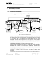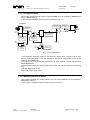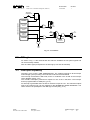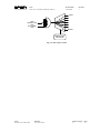
1
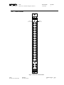
Technical
Information
Manual
Revision n. 1
27 August 2004
MOD. V977
16 CHANNEL
I/O Register (Status A)
MANUAL REV.1
NPO:
00118/01:V977X.MUTX/01
CAEN will repair or replace any product within the guarantee period if the Guarantor declares
that the product is defective due to workmanship or materials and has not been caused by
mishandling, negligence on behalf of the User, accident or any abnormal conditions or
operations.
CAEN declines all responsibility for damages or
injuries caused by an improper use of the Modules
due to negligence on behalf of the User. It is strongly
recommended to read thoroughly the CAEN User's
Manual before any kind of operation.
CAEN reserves the right to change partially or entirely the contents of this Manual at any time
and without giving any notice.
Document type:
User's Manual (MUT)
Title:
Mod. V977 16 Channel I/O Register (Status A)
Revision date:
27/08/2004
Revision:
1
TABLE OF CONTENTS
1.
OVERVIEW ............................................................................................................................................................................5
1.1.
2.
3.
SPECIFICATIONS ...............................................................................................................................................................6
2.1.
PACKAGING ...................................................................................................................................................................6
2.2.
EXTERNAL COMPONENTS............................................................................................................................................6
2.3.
INTERNAL COMPONENTS..............................................................................................................................................7
2.4.
POWER REQUIREMENTS...............................................................................................................................................7
2.5.
TECHNICAL SPECIFICATION TABLES..........................................................................................................................7
2.6.
FRONT PANEL................................................................................................................................................................8
OPERATING MODES .........................................................................................................................................................9
3.1.
4.
M ODULE DESCRIPTION.................................................................................................................................................5
FUNCTIONAL DESCRIPTION .........................................................................................................................................9
3.1.1.
I/O register mode........................................................................................................................................... 10
3.1.2.
Multihit pattern unit mode............................................................................................................................ 10
3.1.3.
Test channel .................................................................................................................................................... 11
3.2.
OR LOGIC.....................................................................................................................................................................12
3.3.
INTERRUPTER CAPABILITY ........................................................................................................................................12
VME INTERFACE ............................................................................................................................................................ 14
4.1.
A DDRESSING CAPABILITY .........................................................................................................................................14
4.2.
DATA TRANSFER CAPABILITY...................................................................................................................................14
4.3.
INPUT SET REGISTER...................................................................................................................................................15
4.4.
INPUT MASK REGISTER...............................................................................................................................................16
4.5.
INPUT READ REGISTER...............................................................................................................................................16
4.6.
SINGLE-HIT READ REGISTER......................................................................................................................................16
4.7.
M ULTI-HIT READ REGISTER.......................................................................................................................................16
4.8.
OUTPUT SET REGISTER...............................................................................................................................................17
4.9.
OUTPUT MASK REGISTER...........................................................................................................................................17
4.10.
INTERRUPT MASK.......................................................................................................................................................17
4.11.
OUTPUT CLEAR REGISTER..........................................................................................................................................17
NPO:
00118/01:V977X.MUTX/01
Filename:
V977_REV1.DOC
Number of pages:
21
Page:
3
Document type:
User's Manual (MUT)
Title:
Mod. V977 16 Channel I/O Register (Status A)
Revision date:
27/08/2004
Revision:
1
4.12.
SINGLEHIT READ-CLEAR REGISTER..........................................................................................................................18
4.13.
M ULTIHIT READ-CLEAR REGISTER...........................................................................................................................18
4.14.
TEST CONTROL REGISTER..........................................................................................................................................18
4.15.
INTERRUPT LEVEL.......................................................................................................................................................19
4.16.
INTERRUPT VECTOR....................................................................................................................................................19
4.17.
SERIAL NUMBER..........................................................................................................................................................19
4.18.
FIRMWARE REVISION..................................................................................................................................................19
4.19.
CONTROL REGISTER...................................................................................................................................................19
4.20.
DUMMY16....................................................................................................................................................................20
4.21.
SOFTWARE RESET .......................................................................................................................................................20
REFERENCES ............................................................................................................................................................................. 21
LIST OF FIGURES
FIG. 2.1: MOD. V977 FRONT PANEL ..............................................................................................................................................8
FIG. 3.1: MOD. V977 CHANNEL STRUCTURE.................................................................................................................................9
FIG. 3.2: I/O REGISTER MODE ........................................................................................................................................................10
FIG. 3.3: MULTIHIT PATTERN UNIT MODE....................................................................................................................................11
FIG. 3.4: TEST CHANNEL.................................................................................................................................................................12
FIG. 3.5: INTERRUPTER SCHEME ....................................................................................................................................................13
FIG. 4.1: MOD. V977 BASE ADDRESS SETTING AND OUTPUT SELECTION...............................................................................15
LIST OF TABLES
TABLE 2.1: POWER REQUIREMENTS................................................................................................................................................7
TABLE 2.2: TECHNICAL FEATURES..................................................................................................................................................7
TABLE 4.1: A DDRESS MAP FOR THE M OD. V977 .......................................................................................................................14
NPO:
00118/01:V977X.MUTX/01
Filename:
V977_REV1.DOC
Number of pages:
21
Page:
4
Document type:
User's Manual (MUT)
Title:
Mod. V977 16 Channel I/O Register (Status A)
Revision date:
27/08/2004
Revision:
1
1. Overview
1.1. Module description
The Mod. V977 is a 1-unit wide VME module that can work either as 16 channel general
purpose I/O Register or as Multihit Pattern Unit; the operating mode is selected via VME
and is signalled via front panel LED.
The module has 16 channels; each channel is provided with one input and one output
connector. Input signals can be indifferently NIM or TTL; an on-board switch allows to
select between NIM and TTL signals for the outputs.
2 LEDs signal the I/O status of each channel.
The module features an additional channel (TEST CHANNEL), which allows to send a
test pulse via a front panel pushbutton. The TEST output signal can be either NIM or TTL,
selected with the same on-board switch of the channels output.
Input signals can be individually masked via VME or globally via a front panel GATE
input. The channel status can be cleared either via VME or via the front panel common
CLEAR input. GATE and CLEAR signals can be indifferently NIM or TTL.
The channels global OR and /OR outputs are available as front panel signals and can be
eventually masked; OR and /OR can be either NIM or TTL, selected with the same onboard switch of the channels output.
The module houses also a fully programmable VME RORA INTERRUPTER that
generates a VME interrupt request when the OR of a selected set of output channels has
a TRUE status.
The module uses the VME P1 and P2 connectors, then it fits into both standard and V430
VMEbus crates.
All the models have a special circuitry that allows the board to be removed from and
inserted in a powered crate without switching the crate off (Live Insertion).
NPO:
00118/01:V977X.MUTX/01
Filename:
V977_REV1.DOC
Number of pages:
21
Page:
5
Document type:
User's Manual (MUT)
Title:
Mod. V977 16 Channel I/O Register (Status A)
Revision date:
27/08/2004
Revision:
1
2. Specifications
2.1. Packaging
1-unit wide VME unit. Height: 6U.
2.2. External components
CONNECTORS:
Function
Type
connector
CHANNELS INPUTS
NIM or TTL
LEMO 00
CHANNELS OUTPUTS
NIM or TTL (selectable) LEMO 00
TEST OUTPUT
NIM or TTL (selectable) LEMO 00
CLEAR INPUT
NIM or TTL
LEMO 00
GATE INPUT
NIM or TTL
LEMO 00
OR and NOT OR OUTPUT NIM or TTL (selectable) LEMO 00
Note
16
Name
I/O STATUS
Color
Green
16
I/O STATUS
1
DTACK
1
TEST
1
PATTERN
1
NIM/TTL
16
16
1
1
1
2
Logic
50 Ω impedance
50 Ω impedance
50 Ω impedance
LEDS
Function
Depends on the module’s programming
status (see § 3.1)
Depends on the module’s programming
status (see § 3.1)
DATA ACKNOWLEDGE command; lights up
each time a VME access is performed.
Lights up as a test signal is sent via
pushbutton
Indicates the module’s programming status;
lights up as the module is programmed in
PATTERN mode (see § 3.1)
Indicates the selected outputs level:
RED=NIM
GREEN=TTL
Green
Green
Green
Yellow
Red/Green
All LEDs also lights up for a while at power ON to indicate that the board is configuring.
PUSHBUTTON:
No.1, to send the TEST input pulse.
NPO:
00118/01:V977X.MUTX/01
Filename:
V977_REV1.DOC
Number of pages:
21
Page:
6
Document type:
User's Manual (MUT)
Title:
Mod. V977 16 Channel I/O Register (Status A)
Revision date:
27/08/2004
Revision:
1
2.3. Internal components
SWITCHES (see Fig. 4.1):
No.4, rotary switches for the module VME Base address selection.
No.1 jumper for the output signal type selection (up: NIM, down: TTL).
2.4. Power requirements
Table 2.1: Power requirements
Power supply
Current absorption
+5 V
2.3A
2.5. Technical specification tables
Table 2.2: Technical features
Packaging
1U-wide VME unit
16 NIM/TTL levels, 50 Ω impedance
16 NIM/TTL levels (selectable),
to be terminated on 50 Ω
Input channels
Output channels
Min. input width
2 ns
I/O delay
T.B.D.
Double pulse resolution
Output rise/fall time
NPO:
00118/01:V977X.MUTX/01
Filename:
V977_REV1.DOC
5 ns
NIM: 1/1 ns; TTL: 3/3 ns
Number of pages:
21
Page:
7
Document type:
User's Manual (MUT)
Title:
Mod. V977 16 Channel I/O Register (Status A)
Revision date:
27/08/2004
Revision:
1
2.6. Front Panel
Mod.
V977
DTACK
OUTPUT
CONNECTORS
INPUT
CONNECTORS
0
0
1
1
2
3
4
5
6
7
8
9
10
11
12
13
14
15
TST
CLR
GATE
PATTERN
OR
/OR
NIM/TTL
STATUS
16 CH A
I/O REGISTER
PATTERN UNIT
Fig. 2.1: Mod. V977 Front Panel
NPO:
00118/01:V977X.MUTX/01
Filename:
V977_REV1.DOC
Number of pages:
21
Page:
8
Document type:
User's Manual (MUT)
Title:
Mod. V977 16 Channel I/O Register (Status A)
Revision date:
27/08/2004
Revision:
1
3. Operating modes
3.1. Functional description
The Mod. V977 is a 16 channel general purpose I/O Register or as Multihit Pattern Unit
The following figure shows the simplified scheme of a single channel:
CONTROL
REGISTER
PATTERN BIT
1
0
OUTPUT MASK
VME REGISTER
D
1
OUTPUT SET
VME REGISTER
Q
1
0
INPUT MASK
VME REGISTER
AR
1
CH #n
OUTPUT
MULTIHIT READ
VME REGISTER
0
D
Q
CH #n
INPUT
SINGLE HIT READ
VME REGISTER
AR
INPUT READ
VME REGISTER
INPUT SET
VME REGISTER
INTERRUPT MASK
VME REGISTER
AR
OR
OUTPUT
GATE
INPUT
OR
OUTPUT
CLEAR
INPUT
CONTROL
REGISTER
GATE MASK BIT
CLEAR OUTPUT
VME REGISTER
TO IRQ
LOGIC
FROM TEST
CHANNEL
LOGIC
CONTROL
REGISTER
OR MASK BIT
Fig. 3.1: Mod. V977 channel structure
The core of each channel is composed by a couple of FLIP -FLOPs, which perform the
memory functions. The two cascaded FLIP -FLOPs, as shown in Fig. 3.1, allow to detect
the following events: none, one or two input hits. The FLIP-FLOPs status of all channels
can be read via VME, in the SINGLEHIT READ REGISTER and MULTIHIT READ
REGISTER, which are related respectively to the first and to the second cascaded
FLIP_FLOP. The content of such register can also be read by accessing the SINGLEHIT
READ-CLEAR REGISTER and MULTIHIT READ-CLEAR REGISTER: in this case the
FLIP -FLOPs are cleared after readout.
The FLIP-FLOPs of all channels can also be cleared both via VME, by accessing the
CLEAR OUTPUT REGISTER, and via the front panel CLEAR signal.
The FLIP FLOPs are set either via an input hit or via VME write access (INPUT SET
REGISTER). By accessing the CLEAR OUTPUT REGISTER, the INPUT SET
REGISTER is cleared.
The capabilty of receiving input hits can be masked via VME through the INPUT MASK
REGISTER (individually for each channel), or via the input GATE signal (common to all
channels), which can be masked in its turn.
The status of the inputs can also be read directly vi a VME in the INPUT READ
REGISTER.
The status of the channel LEDs and of the outputs depend on the module’s programming.
NPO:
00118/01:V977X.MUTX/01
Filename:
V977_REV1.DOC
Number of pages:
21
Page:
9
Document type:
User's Manual (MUT)
Title:
Mod. V977 16 Channel I/O Register (Status A)
Revision date:
27/08/2004
Revision:
1
3.1.1. I/O register mode
The module operates as I/O register if the PATTERN bit of the CONTROL REGISTER is
set to 0 (default setting).
In this case the simplified channel scheme is shown in Fig. 3.2.
PATTERN = 0
OUTPUT MASK
VME REGISTER
OUTPUT SET
VME REGISTER
INPUT MASK
VME REGISTER
1
CH #n
OUTPUT
D
Q
CH #n
INPUT
SINGLE HIT READ
VME REGISTER
AR
INPUT READ
VME REGISTER
INPUT SET
VME REGISTER
AR
to OR and IRQ
LOGIC
GATE
INPUT
CONTROL
REGISTER
GATE MASK BIT
CLEAR
INPUT
CLEAR OUTPUT
VME REGISTER
Fig. 3.2: I/O register mode
In this operating mode the output of one channel is active when a single hit (from front
panel or VME generated) is received. The output can also be set by a write access to the
OUTPUT SET REGISTER.
The outputs can also be masked, individually for each channel, through the OUTPUT
MASK REGISTER.
In this operating mode, the two channel LEDs identify the channel status in the following
way:
Left LED: input signal active;
Right LED: output signal active.
3.1.2. Multihit pattern unit mode
The module operates as multihit pattern unit if the PATTERN bit of the CONTROL
REGISTER is set to 1.
In this case the simplified channel scheme is shown in Fig 3.3.
NPO:
00118/01:V977X.MUTX/01
Filename:
V977_REV1.DOC
Number of pages:
21
Page:
10
Document type:
User's Manual (MUT)
Title:
Mod. V977 16 Channel I/O Register (Status A)
Revision date:
27/08/2004
OUTPUT MASK
VME REGISTER
PATTERN = 1
Revision:
1
OUTPUT SET
VME REGISTER
CH #n
OUTPUT
D
INPUT MASK
VME REGISTER
Q
AR
1
D
MULTIHIT READ
VME REGISTER
Q
CH #n
INPUT
SINGLE HIT READ
VME REGISTER
AR
INPUT READ
VME REGISTER
to OR and IRQ
LOGIC
INPUT SET
VME REGISTER
AR
GATE
INPUT
CONTROL
REGISTER
GATE MASK BIT
CLEAR
INPUT
CLEAR OUTPUT
VME REGISTER
Fig. 3.3: Multihit pattern unit mode
In this operating mode the output of one channel is active when a double hit (from front
panel or VME generated) is present. The output can also be set by a write access to the
OUTPUT SET REGISTER.
The outputs can also be masked, individually for each channel, through the OUTPUT
MASK REGISTER.
In this operating mode, the two channel LEDs identify the channel status in the following
way:
Left LED: single hit received;
Right LED: double hit received and output signal active.
3.1.3. Test channel
The module is provided with an extra channel (TEST CHANNEL), which differs from the
others since the input pulse is sent by a pushbutton. The TEST channel is completely
handled by the Test control register (see § 4.20).
NPO:
00118/01:V977X.MUTX/01
Filename:
V977_REV1.DOC
Number of pages:
21
Page:
11
Document type:
User's Manual (MUT)
Title:
Mod. V977 16 Channel I/O Register (Status A)
TEST INPUT
PUSHBUTTON
1
D
Revision date:
27/08/2004
Revision:
1
Q
1
AR
TEST CONTROL REGISTER
TEST CHANNEL
CLEAR BIT
TEST CHANNEL
MASK BIT
TEST
OUTPUT
TEST CHANNEL
READ BIT
FROM
CHANNELS
LOGIC
TEST CHANNEL
INTERRUPT
MASK BIT
OR
OUTPUT
OR
OUTPUT
TEST CHANNEL
OR MASK BIT
CONTROL
REGISTER
OR MASK BIT
TO IRQ
LOGIC
Fig. 3.4: Test channel
3.2. OR logic
As shown in Fig. 3.1 the channels OR and /OR are available as front panel signals and
can be eventually masked;
Also the TEST signal participates to the OR logic (it can also be masked).
3.3. Interrupter capability
The Mod. V977 house a VME INTERRUPTER. The module responds to D16 Interrupt
Acknowledge cycles providing a word whose 8 LSB are the STATUS/ID.
The interrupt STATUS/ID is 8-bit wide, and it is contained in the 8 LSB of the Interrupt
Vector Register (see § 4.16).
The module’s interrupter produces its request on one of the 7 IRQ lines. The interrupt
level is programmable via VME (see § 4.15).
An Interrupt is generated when the OR of channels’ output is True. The channels outputs
sent to the interrupt logic can be masked via the INTERRUPT MASK REGISTER. The
TEST channel can participate to the IRQ logic as well (see § 4.10)
NPO:
00118/01:V977X.MUTX/01
Filename:
V977_REV1.DOC
Number of pages:
21
Page:
12
Document type:
User's Manual (MUT)
Title:
Mod. V977 16 Channel I/O Register (Status A)
Revision date:
27/08/2004
Revision:
1
IRQ 1
FROM
CHANNELS LOGIC
FROM
TEST CHANNEL
LOGIC
IRQ7
INTERRUPT LEVEL
VME REGISTER
Fig. 3.5: Interrupter scheme
NPO:
00118/01:V977X.MUTX/01
Filename:
V977_REV1.DOC
Number of pages:
21
Page:
13
Document type:
User's Manual (MUT)
Title:
Mod. V977 16 Channel I/O Register (Status A)
Revision date:
27/08/2004
Revision:
1
4. VME Interface
4.1. Addressing capability
The module works in A32/A24 mode. This means that the module address must be
specified in a field of 32 or 24 bits. The Address Modifiers code recognized by the module
are:
AM=%39:
AM=%3D:
AM=%09:
AM=%0D:
A24
A24
A32
A32
non privileged data access
supervisory data access
non privileged data access
supervisory data access
The module's Base Address is fixed by 4 internal rotary switches housed on two piggyback boards plugged into the main printed circuit board (see Fig. 4.1).
The Base Address can be selected in the range:
0x000000
0x00000000
ßà
ßà
0xFF0000
0xFFFF0000
A24 mode
A32 mode
The address map of the page is shown in table 4.1.
4.2. Data transfer capability
The V977 registers are accessible in D16 mode
Table 4.1: Address Map for the Mod. V977
ADDRESS
REGISTER/CONTENT
ADDR
DATA
R/W
Base + %0000
Base + %0002
Base + %0004
Base + %0006
Base + %0008
Base + %000A
Base + %000C
Base + %000E
Base + %0010
Base + %0012
Base + %0014
Base + %0016
Base + %0018
Base + %001A
Base + %001C
Base + %001E
Base + %0020
Base + %0022
Base + %0024
Base + %0026
Base + %0028
Base + %002A
Base + %002C
Base + %002E
INPUT SET
INPUT MASK
INPUT READ
SINGLEHIT READ
MULTIHIT READ
OUTPUT SET
OUTPUT MASK
INTERRUPT MASK
CLEAR OUTPUT
RESERVED
RESERVED
SINGLEHIT READ-CLEAR
MULTIHIT READ-CLEAR
TEST CONTROL REGISTER
RESERVED
RESERVED
INTERRUPT LEVEL
INTERRUPT VECTOR
SERIAL NUMBER
FIRMWARE REVISION
CONTROL REGISTER
DUMMY REGISTER
RESERVED
SOFTWARE RESET
A24/A32
A24/A32
A24/A32
A24/A32
A24/A32
A24/A32
A24/A32
A24/A32
A24/A32
A24/A32
A24/A32
A24/A32
A24/A32
A24/A32
A24/A32
A24/A32
A24/A32
A24/A32
A24/A32
D16
D16
D16
D16
D16
D16
D16
D16
D16
D16
D16
D16
D16
D16
D16
D16
D16
D16
D16
read/write
read/write
read only
read only
read only
read/write
read/write
read/write
write only
read only
read only
read/write
read/write
read/write
read only
read only
read/write
read/write
write only
NPO:
00118/01:V977X.MUTX/01
Filename:
V977_REV1.DOC
Number of pages:
21
Page:
14
Document type:
User's Manual (MUT)
Title:
Mod. V977 16 Channel I/O Register (Status A)
Revision date:
27/08/2004
Revision:
1
7 8 9
2
BC D
F
0
E
6
A
3 4 5
Rotary switches for
VME address
selection
1
Base address bit <19~16>
Base address bit <23~20>
Base address bit <27~24>
Base address bit <31~28>
Jumper for
output type
selection
(SW2)
SW2
NIM
TTL
Fig. 4.1: Mod. V977 Base address setting and output selection
4.3. Input set register
(Base address + %0000 read/write)
Each register’s bit corresponds to one channel. If one bit is set to 1 the relevant channel
FLIP -FLOP (see § 3.1) is set, regardless the corresponding input connector’s status.
15 14 13 12 11 10 9
8
7 6
5 4 3
2
1 0
INPUT SET
In Multihit pattern unit mode, this register allows to obtain a “double hit” on a channel via
VME, by setting and then resetting two times the corresponding bit in this register.
This register default content is 0x0000.
NPO:
00118/01:V977X.MUTX/01
Filename:
V977_REV1.DOC
Number of pages:
21
Page:
15
Document type:
User's Manual (MUT)
Title:
Mod. V977 16 Channel I/O Register (Status A)
Revision date:
27/08/2004
Revision:
1
4.4. Input mask register
(Base address + %0002 read/write)
Each register’s bit corresponds to one channel. If one bit is set to 1, the related input
signal is “masked”; i.e. if a channel is masked the relevant FLIP -FLOP does not receive
the front panel signal. The FLIP -FLOPs’ Qs can be activated anyway via the relevant bit
in the INPUT SET register (see § 4.3).
15 14 13 12 11 10 9
8
7 6
5 4 3
2
1 0
INPUT MASK
This register default content is 0x0000: all channels inputs are enabled.
4.5. Input read register
(Base address + %0004 read only)
Each register’s bit corresponds to one channel: it reproduces the relevant input
connector’s logic level, regardless the INPUT MASK register’s status.
15 14 13 12 11 10 9
8
7 6
5 4 3
2
1 0
INPUT READ
4.6. Single-hit read register
(Base address + %0006 read only)
Each register’s bit corresponds to one channel: it reproduces the relevant FLIP-FLOPs’
Qs, regardless the OUTPUT MASK register’s status. Each bit is set to one as the
corresponding channel as received one hit (from front panel or VME generated).
15 14 13 12 11 10 9
8
7 6
5 4 3
2
1 0
SINGLEHIT READ
4.7. Multi-hit read register
(Base address + %0008 read only)
Each register’s bit corresponds to one channel. Each bit reproduces the relevant FLIPFLOPs’ Qs, regardless the OUTPUT MASK register’s status. This register is used only if
the module operates in multihit pattern unit mode and signals if one channel has received
a double input hit (from front panel or VME generated).
15 14 13 12 11 10 9
8
7
6
5
4
3
2
1
0
MULTIHIT READ
NPO:
00118/01:V977X.MUTX/01
Filename:
V977_REV1.DOC
Number of pages:
21
Page:
16
Document type:
User's Manual (MUT)
Title:
Mod. V977 16 Channel I/O Register (Status A)
Revision date:
27/08/2004
Revision:
1
4.8. Output set register
(Base address + %000A read/write)
Each register’s bit corresponds to one channel. If one bit is set to 1, the corresponding
channel output is active, regardless the corresponding input connector’s and FLIPFLOPs’ Qs status.
15 14 13 12 11 10 9
8
7 6
5 4 3
2
1 0
OUTPUT SET
This register default content is 0x0000.
4.9. Output mask register
(Base address + %000C read/write)
Each register’s bit corresponds to one channel. If one bit is set to 1, the relevant output is
“masked” and no output signal is produced regardless the FLIP FLOPs status. The output
signal can be produced anyway via the relevant bit in the OUTPUT SET register (see §
4.8).
15 14 13 12 11 10 9
8
7 6
5 4 3
2
1 0
OUTPUT MASK
This register default content is 0x0000: all channels outputs are enabled.
4.10. Interrupt mask
(Base address + %000E read/write)
Each register’s bit corresponds to one channel, and it is “masked” as the corresponding
bit is set to 1. The interrupt request (whose level is set by the INTERRUPT LEVEL
register value) is produced when the OR of the channels non mascherati has a TRUE
status.
15 14 13 12 11 10 9
8
7 6
5 4 3
2
1 0
INTERRUPT MASK
This register default content is 0x0000: all channels are unmasked.
4.11. Output clear register
(Base address + %0010 read/write)
A dummy write access to this register clears all the channels FLIP-FLOP.
NPO:
00118/01:V977X.MUTX/01
Filename:
V977_REV1.DOC
Number of pages:
21
Page:
17
Document type:
User's Manual (MUT)
Title:
Mod. V977 16 Channel I/O Register (Status A)
Revision date:
27/08/2004
Revision:
1
4.12. Singlehit read-clear register
(Base address + %0016 read only)
Each register’s bit corresponds to one channel. This is a different way to access the
SINGLE HIT READ REGISTER: a read access to this register clears the first FLIP -FLOP
(see § 3.1) of all channels.
15 14 13 12 11 10 9
8
7
6
5
4
3
2
1
0
SINGLEHIT READ-CLEAR
4.13. Multihit read-clear register
(Base address + %0018 read only)
Each register’s bit corresponds to one channel. This is a different way to access the
MULTI HIT READ REGISTER: a read access to this register clears the second FLIPFLOP (see § 3.1) of all channels.
15 14 13 12 11 10 9
8
7
6
5
4
3
2
1
0
MULTIHIT READ-CLEAR
4.14. Test control register
(Base address + %001A read/write)
This register handles all the TEST INPUT channel operations.
15 14 13 12 11 10 9
8 7
6
5 4
3
2
1
0
TEST CH CLEAR
TEST CH MASK
TEST CH OR MASK
TEST CH INTERRUPT MASK
TEST CH READ
CLEAR BIT: write only. By setting this bit to 1, the TEST CHANNEL FLIP-FLOP is
cleared.
MASK BIT: read/write. If this bit is set to 1, the TEST output is “masked”: it does not
produce an output signal (default setting = 0).
OR MASK BIT: read/write. If this bit is set to 1, the Q signal of the TEST channel is not
sent to the OR logic (default setting = 0).
INTERRUPT MASK BIT: read/write. If this bit is set to 1, the Q signal of the TEST
channel is not sent to the INTERRUPT logic (default setting = 0).
READ BIT: read only. It reproduces the pushbutton status, regardless the MASK bit
status.
NPO:
00118/01:V977X.MUTX/01
Filename:
V977_REV1.DOC
Number of pages:
21
Page:
18
Document type:
User's Manual (MUT)
Title:
Mod. V977 16 Channel I/O Register (Status A)
Revision date:
27/08/2004
Revision:
1
4.15. Interrupt level
(Base address + %0020 read/write)
The 3 LSB of this register contain the value of the interrupt level (Bits 3 to 15 are
meaningless).
15 14 13 12 11 10 9
8
7 6
5 4 3
2
1 0
LEVEL
Default setting is 0x0; in this case interrupt generation is disabled.
4.16. Interrupt vector
(Base address + %0022 read/write )
This register contains the STATUS-ID that the V977 places on the VME data bus during
the interrupt -acknowledge cycle (Bits 8 to 15 are meaningless ).
15 14 13 12 11 10 9
8
7 6
5 4 3
2
1 0
STATUS/ID
Default setting is 0xDD.
4.17. Serial number
(Base address + %0024 read only)
This word reproduces the module’s serial number.
15 14 13 12 11 10 9
8
7 6
5 4 3
2
1 0
SERIAL NUMBER
4.18. Firmware revision
(Base address + %0026 read only)
This word reproduces the module’s firmware revision in the Rev. X.Y format.
15 14 13 12 11 10 9
8
7 6
X
5 4 3
2
1 0
Y
4.19. Control register
(Base address + %0028 read/write)
This register controls the functions common to all channels.
NPO:
00118/01:V977X.MUTX/01
Filename:
V977_REV1.DOC
Number of pages:
21
Page:
19
Document type:
User's Manual (MUT)
Title:
Mod. V977 16 Channel I/O Register (Status A)
15 14 13 12 11 10 9
8
7
6
5
4
3
2
1
Revision date:
27/08/2004
Revision:
1
0
PATTERN
GATE MASK
OR MASK
PATTERN BIT: read/write;
= 0: the module works as I/O REGISTER (default setting);
= 1: the module works as a MULTIHIT PATTERN UNIT;
GATE MASK: read/write;
= 1: the GATE sent via FRONT PANEL signal is masked (default setting);
= 0: the GATE sent via FRONT PANEL signal is enabled; incoming hits are accepted only
as the GATE is active.
OR MASK: read/write;
= 0: the OR and /OR FRONT PANEL outputs are enabled (default setting);
= 1: the OR and /OR FRONT PANEL outputs are masked.
4.20. Dummy16
(Base address + %002A read/write)
This register allows to perform 16 bit test accesses for test purposes.
Default setting is 0x5555.
4.21. Software reset
(Base address + %002E write only)
A dummy write access to this register allows to generate a single shot RESET of the
module, which restores the default conditions.
NPO:
00118/01:V977X.MUTX/01
Filename:
V977_REV1.DOC
Number of pages:
21
Page:
20
Document type:
User's Manual (MUT)
Title:
Mod. V977 16 Channel I/O Register (Status A)
Revision date:
27/08/2004
Revision:
1
References
[1] VMEbus Specification Manual Revision C.1 October 1985
[2] VMEBus for Physics Application, Recommendations & Guidelines, Vita23-199x, draft 1.0, 22 May
1997.
NPO:
00118/01:V977X.MUTX/01
Filename:
V977_REV1.DOC
Number of pages:
21
Page:
21