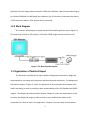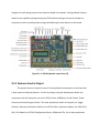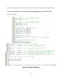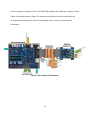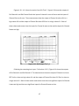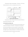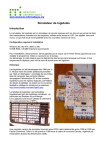
1
ANALOG TO VGA VIDEO INTERFACE BY GREGORY M. REDMAN A technical report submitted to the Graduate School In partial fulfillment of the requirements for the degree Master of Sciences, Engineering Specialization in: Electrical Engineering New Mexico State University Las Cruces, New Mexico March 2011 ”Analog to VGA Video Interface,” a project report prepared by Gregory M. Redman in partial fulfillment of the requirement for the degree, Master of Science in Electrical Engineering, has been approved and accepted by the following: Linda Lacey Dean of the Graduate School Paul M. Furth Chair of the Examining Committee Date Committee in charge: Dr. Paul M. Furth, Chair Dr. Steve Stochaj Patricia Sullivan ii DEDICATION Dedicated to all my supporters. To all my family and friends, past and present, who have loved and supported me throughout my life. iii ACKNOWLDEGEMENTS It has been just over 8 years since I started college at NMSU, working towards graduating with my graduate degree. I have learned many things in my time spent at NMSU. One important thing I learned about is time. It takes well spent time to become smarter and wiser, and in hind sight, that time generally flies. First of all, I would like to thank God for everything he has given me throughout my life: family, friendship, faith, and anything else I have needed to survive and succeed. I would like to thank my family for all the love and support they have given me, not only through these years of college, but throughout all the years of my life. Without that love and support I would never have succeeded in making it this far. I would like to thank all my friends for their friendship and support. Without you I would never have made it thru all the stressful times I have gone through, college would not have been as fun, and I would not have had as many wonderful experiences as I have had in my life so far. I would like to thank my advisor Dr. Paul M. Furth for his guidance and wonderful teaching abilities, from which I have learned so much. His deep faith in God is an inspiration to all. I would like to thank Dr. Steve Stochaj for agreeing to be a part of my committee. I would also like to thank Patricia Sullivan for also agreeing to be a part of my committee, for iv getting me help on my master’s project, and for helping to get me a job at White Sands when I graduated with my Bachelors. I would like to thank Mr. Marty Small from Calculex for getting someone to make the needed modifications to the daughter card used in this project. I would like to thank Mr. Alejandro Pena for fabricating a custom circuit board for me that I needed for this project. Lastly, I would like to thank Professor Lynn Kelly for taking the time to: answer my questions for this project when she could, giving me advice when I got stuck on the project, providing me with resources when I needed them, and teaching me new things in the area of Digital Design. v VITA Education 2003 – 2008 Bachelors of Science in Electrical Engineering New Mexico State University, Las Cruces, New Mexico Since 2008 Masters of Science in Electrical Engineering New Mexico State University, Las Cruces, New Mexico Field of Study Major Field: Electrical Engineering (Microelectronics / VLSI Design / Communications) vi ABSTRACT ANALOG TO VGA VIDEO INTERFACE BY GREGORY M. REDMAN Master of Science in Electrical Engineering New Mexico State University Las Cruces, New Mexico, 2011 Dr. Paul M. Furth, Chair Place: Thomas & Brown Room-207 Date: December 2, 2011 Time: 8:00 AM The main goal of this project is to design an easy-to-use interface that displays on a VGA monitor the image incident on a CMOS imager and provide signals needed to control the CMOS imager. The interface needs to take the input frame from the imager with a resolution of 80 x 60 pixels and output the frame onto a VGA monitor at a resolution of 640 x 480 pixels. The interface is implemented using an Altera DE2 Development Board with a Terasic THDB-ADA Daughter Card, and a custom circuit board used to allow access to unused pins on the two header connectors located on the DE2 board. Quartus II Design Software and SoPC Builder were the two main design tools used to program the interface. vii The design utilizes toggle switches and pushbutton switches on the DE2 board as the means of controlling the integration time and reset signals for the CMOS imager, respectively. The daughter card was modified so that it would not block dc voltages. The two D/A converter outputs and unused output pins on the header connectors are used as control outputs for the CMOS imager. After testing the interface design block by block, two of the three major stages of the interface can be shown as working properly. These stages are the input stage, and the VGA controller stage. The middle stage, where the frames from the imager use the SRAM as a buffer, partially works but still needs further improvement. viii TABLE OF CONTENTS LIST OF TABLES ................................................................................................................................................. xii LIST OF FIGURES ............................................................................................................................................. xiii 1 Introduction ................................................................................................................................................. 1 1.1 Motivation................................................................................................................................................ 1 1.2 Problem Statement .............................................................................................................................. 1 1.2.1 Definition of Interface ............................................................................................................ 2 1.2.2 Description of Project ............................................................................................................. 2 1.2.3 Block Diagram ........................................................................................................................... 3 1.3 Organization of Technical Report................................................................................................... 3 2 Background................................................................................................................................................... 5 2.1 Altera DE2 Development Board ...................................................................................................... 5 2.1.1 Main Features ............................................................................................................................ 5 2.1.2 Features Used in Project ........................................................................................................ 7 2.2 Terasic THDB-ADA Daughter Card ................................................................................................ 8 2.2.1 Main Features ............................................................................................................................ 8 2.2.2 Features Used in Project ..................................................................................................... 10 2.3 Software Tools .................................................................................................................................... 10 2.3.1 Quartus II .................................................................................................................................. 10 2.3.1.1 Description .............................................................................................................. 11 2.3.1.2 Purpose ..................................................................................................................... 13 2.3.2 SoPC Builder ............................................................................................................................ 13 2.3.2.1 Description .............................................................................................................. 14 2.3.2.2 Purpose ..................................................................................................................... 15 2.4 VGA Standard ...................................................................................................................................... 15 ix 2.4.1 Basic Operation ...................................................................................................................... 16 2.4.2 Synchronization Signals...................................................................................................... 17 2.5 CMOS Imagers ..................................................................................................................................... 19 2.5.1 Pixels .......................................................................................................................................... 20 2.5.2 Arrays......................................................................................................................................... 21 2.5.3 Readout and Timing ............................................................................................................. 21 3 Design and Implementation ............................................................................................................. 22 3.1 Requirements ...................................................................................................................................... 23 3.1.1 Problem Statement ............................................................................................................... 23 3.1.2 Constraints ............................................................................................................................... 23 3.1.3 Inputs and Outputs ............................................................................................................... 24 3.1.4 Block Diagram ........................................................................................................................ 25 3.2 VHDL and System Design................................................................................................................ 25 3.2.1 SoPC Design ............................................................................................................................. 25 3.2.2 VHDL Code ............................................................................................................................... 26 3.3 Hardware Design ............................................................................................................................... 28 3.3.1 Modifications to Development Board............................................................................ 29 3.3.2 Modifications to Daughter Card....................................................................................... 29 3.3.3 Final Design Block Diagram .............................................................................................. 30 4 Test Setup and Procedures ................................................................................................................ 32 4.1 Test Setup ............................................................................................................................................. 32 4.1.1 Required Equipment ............................................................................................................ 32 4.1.2 Interface setup........................................................................................................................ 33 4.2 System Test Procedures .................................................................................................................. 34 4.2.1 JTAG Programming ............................................................................................................... 34 4.2.2 Active Serial Mode Programming ................................................................................... 35 4.3 Subsystem Test Procedures........................................................................................................... 37 4.3.1 Testing D/A Converter ........................................................................................................ 37 x 4.3.1.1 D/A Test 1 ................................................................................................................ 38 4.3.1.2 D/A Test 2 ................................................................................................................ 39 4.3.2 Testing A/D Converter ........................................................................................................ 40 4.3.3 Testing VGA Controller ....................................................................................................... 44 4.3.4 Testing SRAM .......................................................................................................................... 44 4.4 Test Results .......................................................................................................................................... 44 4.4.1 Results from D/A and A/D tests ...................................................................................... 45 4.4.2 Results from interface test................................................................................................. 51 5 Discussion and Conclusions .............................................................................................................. 56 5.1 Discussion of Test Results .............................................................................................................. 56 5.1.1 A/D and D/A test ................................................................................................................... 56 5.1.2 Interface test ........................................................................................................................... 57 5.2 Summary of Work .............................................................................................................................. 58 5.3 Future Work......................................................................................................................................... 59 6 References .................................................................................................................................................. 61 xi LIST OF TABLES Table 2.1: DE2 Board Information from [16] ............................................................................................. 6 Table 2.2: Avalon Interfaces based on [18].............................................................................................. 15 Table 2.3: HSYNC & VSYNC Signal Regions based on [10] ................................................................. 17 xii LIST OF FIGURES Figure 1.1: Basic Interface System ................................................................................................................. 3 Figure 2.1: DE2 Peripherals Layout from [3] ............................................................................................. 7 Figure 2.2: Daughter Card Front View from [17] ..................................................................................... 9 Figure 2.3: Quartus II Design Flow from [5] ............................................................................................ 11 Figure 2.4: Quartus II Main Project Screen GUI...................................................................................... 12 Figure 2.5: SoPC Builder Project Main Screen GUI................................................................................ 13 Figure 2.6: VGA Screen Refresh Process from [10]............................................................................... 16 Figure 2.7: HSYNC Signals from [10] .......................................................................................................... 18 Figure 2.8: VSYNC Signals from [10] .......................................................................................................... 19 Figure 2.9: 4T APS Design based on [12] .................................................................................................. 20 Figure 2.10: APS Block Diagram from [12] .............................................................................................. 22 Figure 3.1: Interface Basic Diagram ............................................................................................................ 24 Figure 3.2: SoPC System .................................................................................................................................. 25 Figure 3.3: VHDL Code Excerpts .................................................................................................................. 27 Figure 3.5: THDB-ADA to DE2 Interface Layout .................................................................................... 29 Figure 3.4 : Daughter Card Header Connection Schematic from [19] ........................................... 29 Figure 3.6: Daughter Card Modifications Schematic based on [19] ............................................... 30 Figure 3.7: Interface Final Diagram ............................................................................................................ 31 xiii Figure 4.1: Programmer JTAG Screenshot ............................................................................................... 35 Figure 4.2: Programmer ASP Screenshot ................................................................................................. 36 Figure 4.3: ADA Utility Screenshot .............................................................................................................. 38 Figure 4.4: DAC Input Code ............................................................................................................................ 40 Figure 4.5: ADC out to DAC in Code ............................................................................................................ 41 Figure 4.6: ADA Utility CH A Input .............................................................................................................. 45 Figure 4.7: ADA Utility CH A Output ........................................................................................................... 45 Figure 4.8: ADA Utility CH B Input .............................................................................................................. 46 Figure 4.9: ADA Utility CH B Output ........................................................................................................... 46 Figure 4.10: D/A Output Test 2_1 ................................................................................................................ 47 Figure 4.11: D/A Output Test 2_2 ................................................................................................................ 48 Figure 4.12: A/D Test Output ........................................................................................................................ 48 Figure 4.13: A/D THDI_IN Measurement .................................................................................................... 49 Figure 4.14 : A/D THDIN Measurement ..................................................................................................... 49 Figure 4.15: A/D THDOUT Measurement.................................................................................................... 50 Figure 4.16: A/D RMSIN Measurement....................................................................................................... 50 Figure 4.17: A/D RMSOUT Measurement .................................................................................................... 50 Figure 4.18: A/D tdelay Measurement .......................................................................................................... 51 Figure 4.19: Interface Output for Sinusoidal Input ............................................................................... 52 xiv Figure 4.20: Interface Output for Positive Ramp Input....................................................................... 53 Figure 4.21: Reset Output ............................................................................................................................... 54 Figure 4.22: Clock Output ............................................................................................................................... 54 Figure 4.23: Integration Time Control Output........................................................................................ 55 xv 1 Introduction 1.1 Motivation The problem with testing custom imagers and only seeing voltage values for each pixel, is that creating an image in your mind with only voltages as a reference is a hard task to accomplish. Doing so while looking at the data of still shots is hard, but doing that with realtime data is next to impossible. What about actually being able to see what the imager is seeing? This project was conducted in order to provide that luxury of being able to “just see” the image, not, still shot by still shot, but in real-time. 1.2 Problem Statement Designing an interface in which a custom CMOS imager can be connected to show its data on a monitor, at first, can seem like an easy task. Take the pixel voltage values from the imager and point them to the corresponding pixels on the monitor. However, when you look at the problem more in-depth, a few issues will become apparent, thus turning this initial simple design problem into a complex project. First issue, the resolution of these custom imagers will be at a max of 80 pixels by 60 pixels, and a VGA monitor’s resolution is 640 pixels by 480 pixels. Therefore, streaming the data of each pixel straight to the monitor is out of the question. Secondly, since the imager resolution can vary from one imager to another, this interface needs to have the capability of easily varying the incoming resolution. Lastly, this interface will require the use of more than one clock so timing will be a big factor in getting the interface to work properly. 1 1.2.1 Definition of Interface According to the Merriam-Webster dictionary an interface is “the place at which independent and often unrelated systems meet and act on or communicate with each other [1].” 1.2.2 Description of Project This project was designed using two off-the-shelf circuit boards (an Altera DE2 Development board and a Terasic THDB-ADA Daughter Card) and one custom circuit board to implement the intended interface. This interface is broken up into three distinguishable blocks: input stage, memory, and output stage. The locations of each block are spread across all three circuit boards based on the resources located on each. The input stage is broken up between the DE2 board and the Daughter Card. The memory block is located on the DE2 board and the output stage is located amongst all three boards. Because there are issues causing the design of this interface to be difficult and not straightforward, a software tool was used called SoPC builder (System on a Programmable Chip) which is capable of simplifying portions of the design. Using its graphical user interface (GUI), this SoPC builder software allows the designer to plug together pre-designed and/or custom system components to build a system that meets their needs. This software will then generate a custom HDL (Hardware Description Language) code that is used to program the DE2 board to become the designed system. What this interface was designed to do is the following: provide the imager with a clock signal, reset signal, and integration time control signals for its operation; receive the output 2 pixel data from the imager whose resolution is 80 pixels x 60 pixels, take this data and enlarge it to a frame of 640 pixels by 480 pixels (the resolution of a VGA monitor), and output the data to a VGA connection where a VGA monitor will be connected. 1.2.3 Block Diagram This interface will belong to a system that will look something like the one in Figure 1.1. This system will include: a VGA monitor, VGA cable, CMOS imager and the Interface itself. Figure 1.2.3: Basic Interface System 1.3 Organization of Technical Report This document is divided into 4 major chapters: background information, design and implementation, test setup and procedures, and discussion and conclusions. The background information chapter, Chapter 2, covers an explanation of all components and software tools used in the design, as well as providing a basic understanding of the VGA Standard and CMOS Imagers. The design and implementation chapter, Chapter 3, covers the requirements of this interface, the design and program codes, as well as some modifications made to the components for them to work in this application. Chapter 4, the test setup and procedures 3 section, covers all of the tests conducted on the interface, the procedures for those tests and their results. The final chapter, Chapter 5, covers the discussion of the test results, conclusions, a summary of the work conducted in this project and some further discussion about future work to make improvements. 4 2 Background This chapter provides an overview of all the major components that make up this interface, including some information on the VGA standard. Another topic covered in this chapter is the software tools used in the design. Lastly, some information is provided on what makes up a CMOS imager and how it works. 2.1 Altera DE2 Development Board A development board is a printed circuit board on which an FPGA (Field Programmable Gate Array) and multiple hardware peripherals (Toggle Switches, 7-Segment Displays, SRAM, LEDs, etc.) reside. An FPGA is an integrated circuit made up of an array of logic devices where “the logic network can be programmed into the device after its manufacture [2].” FPGA’s are generally configured by writing code in a HDL (Hardware Description Language); this project was designed using VHDL (Very-high speed integrated circuit Hardware Description Language). On the development board, the peripheral devices are connected through the FPGA, thus allowing “the user to configure the FPGA to implement any system design [3]” of their choice. 2.1.1 Main Features The Altera DE2 board has a large variety of onboard hardware peripherals, all of which are listed in Table 2.1 and shown in Figure 2.1. With the amount of peripherals on this board one can only imagine the variety of systems that can be implemented. A user could build anything from a simple circuit that controls LEDs with toggle switches or displays a message on the LCD display, to a Karaoke Machine or Ethernet Transmitter/Receiver. With the onboard expansion headers and all the other I/O interfaces (USB, Ethernet, RS232, Video In/Out, etc.) 5 the possibilities only increase by providing the capability to easily connect an external device that can interface with the development board. DE2 Board Information Feature Description FPGA Cyclone II EP2C35F672C6 with EPCS16 16-Mbit serial configuration device I/O Interfaces Built-in USB-Blaster for FPGA configuration Line In/Out, Microphone In (24-bit Audio CODEC) Video Out (VGA 10-bit DAC) Video In (NTSC/PAL/Multi-format) RS232 Infrared port PS/2 mouse or keyboard port 10/100 Ethernet USB 2.0 (type A and type B) Expansion headers (two 40-pin headers) Memory 8 MB SDRAM, 512 KB SRAM, 4 MB Flash SD memory card slot Displays Eight 7-segment displays 16 x 2 LCD display Switches and LEDs 18 toggle switches 18 red LEDs 9 green LEDs Four debounced pushbutton switches Clocks 50 MHz clock 27 MHz clock External SMA clock input Table 2.1.1: DE2 Board Information from [16] The board provides the capability of using two different onboard clocks to run the designed systems, as well as a connection for an external clock source. This variability allows 6 designers to easily design systems that require multiple clock speeds. Having onboard memory allows for the capability of programming the FPGA without having to connect the board to a computer, as well as providing data storage and buffering for other devices on the board. Figure 2.1.1: DE2 Peripherals Layout from [3] 2.1.2 Features Used in Project This project does not require the use of all the peripheral components on the board but it does require multiple peripherals. As with any design using this development board, the components that will always be use are the FPGA, Clocks, USB Blaster Port & Chipset, Power Connector and Run/Program Switch. The other peripherals used in this project are: Toggle Switches, Debounce Pushbutton Switches, the SD Card Slot, Expansion Headers, the VGA 10-bit DAC, VGA Video Port, EPCS16 Configuration Device, SRAM and LEDs. All of these peripherals 7 can be seen in Figure 2.1, which shows the layout of the DE2 board and the locations of the hardware devices. 2.2 Terasic THDB-ADA Daughter Card A daughter card is a circuit board that is an extension of a mainboard. It usually only has a direct connection to the mainboard and doesn’t connect thru a general-purpose communications port, such as a USB or RS232 connection. In our case the daughter card connects to the mainboard (DE2) thru two 40-pin expansion headers. The purpose of a daughter card is to provide the user of a mainboard, such as the DE2, with extra peripherals that are not found on the mainboard. This particular daughter card is a High-speed ADC/DAC Card. 2.2.1 Main Features The THDB-ADA card has Dual ADC (Analog-to-Digital Conversion) channels “with 14-bit resolution and a data rate up to 65 MSPS [4]” and Dual DAC (Digital-to-Analog Conversion) channels “with 14-bit resolution and a data rate up to 125 MSPS [4].” The card runs on one of three clocks: 100MHz oscillator, external clock input or a PLL source from the GPIO (General Purpose Input/Output) interface. There are two different modes that the DAC can be operated in: Dual-Port Mode and Interleaved Mode. In Dual-Port Mode the converter is capable of transmitting different data on the two different ports with different update rates. In Interleaved mode, which is especially good for processing data in communication applications, an incoming data stream with 8 interleaved data (I1,Q1,I2,Q2,…) will be “demuxed into its original I and Q data and latched [4]” (Ch. 1 data stream- I1,I2,I3,…; Ch. 2 data stream-Q1,Q2,Q3,…). The ADC also has more than one mode of operation which is controlled by the input of an internal MUX. The ADC can either: have the input of channel A go directly to channel A and channel B input directly to channel B output, have the input of channel A go to the channel B output and the channel B input to the channel A output or have the channel A and B inputs both sent to the channel A output (e.g. Input A Data Stream: A1,A2,A3,…; Input B Data Stream: B1,B2,B3,…; Output A Data Stream: A1,B1,A2,B2,A3,B3,…) [4]. Figure 2.2.1: Daughter Card Front View from [17] 9 Some of the settings on this board are changed by moving jumpers and some of the settings are done by asserting certain input pins high or low. As you can see in Figure 2.2, there are a set of jumpers for the clock settings of each channel and a set of jumpers to control the MUX in the ADC. The other settings such as: Mode Select for the DAC, ADC output on or off, daughter card power on or off and input write signals for the DAC, are all controlled by asserting their corresponding enable pins high or low. 2.2.2 Features Used in Project This interface project only requires the use of one ADC channel using the PLL as the clock, where the channel A input is muxed directly to the channel A output and the channel B input is muxed directly to the channel B output. The DAC will be used in Dual-Port Mode where both outputs will be utilized and just like the ADC. The clock input will also be the PLL input. 2.3 Software Tools As stated earlier, FPGAs are generally configured by writing code in a HDL and the code is then programmed into the FPGA. Where is this code written? How is the FPGA programmed? That is where design software comes into the picture. Software such as Quartus II and one of its system integration tools, the SoPC builder. 2.3.1 Quartus II Altera’s “Quartus II design software is a multiplatform design environment that easily adapts [5]” to a variety of design needs. “It is a comprehensive environment for SoPC design [5].” This section will cover a basic understanding of the Quartus II design software. 10 Figure 2.3.1: Quartus II Design Flow from 2.3.1.1 Description Quartus II contains a host of system-level tools that allow the user the capability of using whatever tools that meet their needs beyond what Quartus itself offers. The four main system-level tools in this design environment are: ModelSim, DSP Builder, SoPC builder (more detail in Section 2.3.2) and Qsys [6]. ModelSim is a software tool that allows the user to simulate all of their FPGA designs. The DSP Builder software tool allows the user to use the “industry-standard MathWorks Simulink tools” to build Model Files and from that “generate VHDL files and Tcl scripts for synthesis, hardware implementation, and simulation [7] .” Both the SoPC builder and Qsys are “powerful system development tools. [8]“ They enable the user to “define and generate a complete SoPC in much less time than using traditional, manual 11 integration methods [8].” Qsys is the new and improved SoPC Builder tool. It performs better; it enables the user to better reuse designs, and has faster verification of circuits when compared to the SoPC builder [6]. Quartus II lets a user either use its GUI or Command-Line Interface when stepping thru phases of design in their projects. Figure 2.3 shows the design flow in Quartus II and Figure 2.4 shows the Quartus II GUI when a project is first opened. Figure 2.3.1.1: Quartus II Main Project Screen GUI 12 2.3.1.2 Purpose As previously stated in this section, Quartus II provides a variety of tools for use when designing a system using FPGAs. The DE2 board is also a product of Altera; thus, it is optimized for use with Altera’s Quartus II Design software. Since Quartus II provides a user friendly GUI and a variety of tutorials and demonstrations, it is a great choice of design software to help ease the design process. 2.3.2 SoPC Builder Section 2.3.1.1 of this text covers the system-level tools included in the Quartus II design environment, the SoPC builder is one of these tools. This section will cover the SoPC Builder in more detail. Figure 2.3.2: SoPC Builder Project Main Screen GUI 13 2.3.2.1 Description The SoPC Builder is a general-purpose tool for creating systems that may or may not contain a processor. What it does is to “automate the task of integrating hardware components [8].” Traditionally, a designer would have to manually write HDL code to create components needed for their system, as well as code that wires all the components together to create the system as a whole. In the SoPC Builder using a GUI, the user specifies the system components called IP cores (Intellectual Property cores) and the way they need to interconnect and the SoPC Builder will generate the HDL files “that define all component of the system, and a top-level HDL file that connects all the components together [8].” Figure 2.5 shows the SoPC Builder GUI when it is opened to a system. There are a variety of already-designed system components provided in the software tool, but there is also the capability of designing custom system components as well. Each system component is connected to each other physically by Avalon interfaces through what is called an Avalon interconnect fabric [8]. The Avalon interconnect fabric “is a flexible, partial crossbar fabric that connects master and slave components [9].” Different from a bus architecture, which requires all master components to fight for the bus regardless of the actual slave device to which it requires access, the partial crossbar system interconnect fabric allows for the arbiter to select “among all the requesting masters [9].” This means that if there isn’t more than one master trying to use a slave at the same time, there is no conflict that the arbiter has to resolve [9]. An Avalon interfaces behavior is described using properties. Table 2.2 shows all the various interfaces. 14 Interface Avalon Memory Mapped Interface (Avalon-MM) Avalon Streaming Interface (Avalon-ST) Description An address-based read/write interface typical of master–slave connections. An interface that supports the unidirectional flow of data, including multiplexed streams, packets, and DSP data. Avalon Memory Mapped Tristate An address-based read/write interface to support offInterface chip peripherals. Multiple peripherals can share data and address buses to reduce the pin count of an FPGA and the number of traces on the PCB. Avalon Clock An interface that drives or receives clock and reset signals to synchronize interfaces and provide reset connectivity. Avalon Interrupt An interface that allows components to signal events to other components. Avalon Conduit An interface that allows signals to be exported out at the top level of an SOPC Builder system where they can be connected to other modules of the design or FPGA pins. Table 2.3.2.1: Avalon Interfaces based on [18] 2.3.2.2 Purpose The previous section illustrates the fact that the SoPC Builder automates the process of integrating hardware components and it generates the required HDL files to configure the FPGA. Using the SoPC builder allows the user to create a design using a GUI which can typically prove to be easier and quicker than just writing code. The software also provides some good tutorials and demonstrations that illustrate the capabilities of the SoPC Builder which could allow the designer to use them as a template for their own design. 2.4 VGA Standard “VGA is a video display standard introduced in the late 1980s in IBM PCs and it is widely supported by PC graphics hardware and monitors [10].” Its original design was for use with CRT 15 (cathode ray tube) monitors; however, most modern LCDs (liquid crystal displays) include a VGA port. The resolution of these monitors is 640 pixel columns x 480 pixel rows. For these monitors to work, 5 signals are required [11]: horizontal sync, vertical sync, red analog signal (00.7 v), green analog signal (0-0.7 v) and a blue analog signal (0-0.7 v). By changing the voltages of the three RGB signals all the other colors are produced. 2.4.1 Basic Operation The VGA standard has a specific process for drawing the screen on a monitor. The process starts at the upper left corner of the monitor and moves one pixel at a time across the screen from left to right; this is called a horizontal scan. At the end of the first row of pixels the screen points to the next row of pixels starting again from the left most column of pixels, this is called a horizontal retrace [11] [10]. Once the entire screen is drawn, the whole process starts over again from the top left corner; this is called a vertical retrace. This whole refresh process is shown in Figure 2.6. Figure 2.4.1: VGA Screen Refresh Process from [10] 16 Region hsync vsync Region where the pixels are actually Region where the horizontal lines Display displayed on the screen. The length are actually displayed on the screen. of this region is 640 pixels. The length of this region is 480 lines. Region in which the column address Region that the row address returns returns to the left edge. The video to the top of the screen. The video Retrace signal should be disabled (i.e. black), signal should be disabled, and the and the length of this region is 96 length of the region is 2 lines. pixels Region that forms the right border Region that forms the bottom of the display region. It is known as border of the display region. It is Right Border (hsync) the front porch (i.e., porch before also known as the front porch (i.e., Bottom Border (vsync) retrace). The video signal should be porch before retrace). The video disabled, and the length of this signal should be disabled, and the region is 16 pixels. length of this region is 10 lines. Region that forms the left border of Region that forms the top border of the display region. It is also known the display region. It is also known Left Border (hsync) as the back porch (i.e., porch after as the back porch (i.e., porch after Top Border (vsync) retrace). The video signal should be retrace). The video signal should be disabled, and the length of this disabled, and the length of this region is 48 pixels. region is 33 lines. Table 2.4.1: HSYNC & VSYNC Signal Regions based on [10] 2.4.2 Synchronization Signals The two control signals: horizontal sync (hsync) and vertical sync (vsync) tell the monitor when to do a horizontal and vertical retrace respectively. One period of hsync and one period of vsync have 4 distinct regions, all of which are listed in Table 2.3 and can be seen in Figures 2.7 and 2.8, respectively. 17 Figure 2.4.2: HSYNC Signals from [10] When considering timing for the VGA synchronization signals some simple calculations are necessary. The pixel rate is determined from 3 factors: - # of pixels in a horizontal scan line, - # of lines in a screen, and - # of screens per second. with a resolution of 640 x 480 the pixel rate can be calculated as follows [10]: 18 . For VGA Figure 2.4.2: VSYNC Signals from [10] 2.5 CMOS Imagers Image sensors are devices that convert the apparent scene into electrical signals by means of an array of pixels. There are two basic kinds of CMOS imagers: passive and active. Passive-pixel sensors (PPS) generally carry a significant amount of noise due to the signal being carried thru several different components on chip prior to being amplified. Because of the noise additional processing is required to reduce the noise. Active-pixel sensors (APS) have a reduction in noise from passive-pixel sensors due to an extra amplifier in each pixel. Two measurements are generally made on each pixel: one when the imager is reset and the second after the image is captured. Taking the difference of these two measurements helps to cancel the noise associated with each pixel, and from this concept this type of CMOS Imager got its name [12]. 19 2.5.1 Pixels CMOS Image Sensors, both passive and active, have many different architectures. This interface design is mainly related to the 4T (4 Transistor) APS design. This design can be seen in Figure 2.9, it consists of 4 transistors, a MOScap and a photodiode. The photodiode senses the light incident on it and produces a photocurrent. This photocurrent is then converted to a voltage using a load. Figure 2.5.1: 4T APS Design based on [12] When reset is high, the pixel is in reset mode and the photo diode is pulled towards Vdd – Vthn, where Vthn is the nMOS threshold voltage. When reset is low, the pixel integrates at the rate set by the photo-current Iph and the capacitance C of the. The transfer gate is controlled by the signal Tx which sets the integration time. Tx stays high for the desired integration time and then goes low at the end of sampling mode where the value is stored (or held) on the MOScap. The MOScap is used to protect the data from being lost and to reduce thermal. “The 20 voltage on the MOScap is buffered through a source follower amplifier Msf” and then output to the column line thru the Msel transistor noise [12]. 2.5.2 Arrays As mentioned earlier, imagers are made up of arrays of N pixels x M pixels. The array of pixels acts like an analog memory array since it stores each pixel value within the cell itself. Based on the purpose of the imager and the type of process used to manufacture the imager, the size of the array can be varied. Based on the AMI 0.5µ process and a maximum chip size of 1.5mm x 1.5mm, in general, the size of the arrays will max out around N=80 pixels and M=60 pixels. 2.5.3 Readout and Timing The APS uses a principal known as correlated double sampling to get a better quality image [12]. Correlated double sampling is taking two samples from the same pixel – one immediately after reset and one after the voltage is stored (held) on the MOScap – and then subtracting the two values in order to reduce fixed-pattern noise. Most of the circuitry that controls the readout of an APS is digital, as can be seen in Figure 2.10. The Variable Integration logic block generates 3 different integration times and its outputs are controlled by a 4:1 MUX. The pixel values are read out using the MUX and decoder. When a row is selected by the decoder, one row at a time, each sampled value in that row is moved to the column line, and the value on the column line is then read out using the MUX. 21 Figure 2.5.3: APS Block Diagram from [12] 22 3 Design and Implementation This chapter provides an explanation of the design requirements and constraints, and illustrates the complete design of the analog to VGA video interface. 3.1 Requirements The main requirements of this design are as follows: design an easy to use interface that will show on a VGA monitor the image incident on a CMOS imager and provide the control signals needed to run the CMOS imager (clock, reset, integration time control). 3.1.1 Problem Statement This interface will have to accommodate having an input frame resolution with a max of 80 pixels x 60 pixels and an output frame resolution of 640 pixels x 480 pixels. The interface must allow for the size of the incoming frame resolution to be easily changed since different imagers may have different array sizes. The data input clock is going to be much less than the system clock and the data output clock (i.e. input clock ≈ 1MHz, system clock ≈ 50MHz and output clock ≈ 25MHz). 3.1.2 Constraints There are a few constraints on the design based on the available resources on the DE2 board. One constraint is the number of available pins we are able to physically get to when using the daughter card with the DE2 board. The daughter card takes up both 40 pin headers, which are the only way to connect to the FPGA pins based on the DE2 design. Another constraint is that the daughter card only has two ADC inputs; therefore we cannot use full RGB VGA and we will have to settle with monochrome VGA. The last constraint is with the daughter 23 card. The inputs and outputs on the card block DC, so anytime the inputs to the ADC or DAC are at a DC value, the outputs will be zero. 3.1.3 Inputs and Outputs For the video feed, the input from the imager will be an analog voltage signal between 0V and 0.7V. The output video feed from the interface should also be an analog voltage signal between 0V and 0.7V. The outputs for the integration time control signals should be either a 0V or 3.3V dc voltage controlled by toggle switches on the DE2 board. The reset signal will either be a 3.3V dc voltage or a 0V dc voltage controlled by a pushbutton switch on the DE2 board. The output clock for the imager will be a 50MHz or 27MHz clock signal that comes from the oscillator on the DE2 board. Figure 3.1.3: Interface Basic Diagram 24 3.1.4 Block Diagram Figure 3.1 shows an overall view of what the interface should look like based on the specifications mentioned earlier in this chapter. 3.2 VHDL and System Design The design of this interface consists of a SoPC builder system design and VHDL code that are used to program the DE2 Development Board. 3.2.1 SoPC Design Figure 3.2: SoPC System As mentioned earlier, the SoPC system consists of IP cores that are connected together to form some sort of system. Figure 3.2 shows the system used for this Interface project. There are 9 cores used: Nios II Processor, On-Chip Memory (RAM or ROM), Clock Signals for the DE-Series Board Peripherals, SRAM/SSRAM Controller, RGB Resampler, Scaler, Dual-Clock FIFO, and a VGA Controller. 25 The Nios II Processor is what controls the on chip memory, clocks, and SRAM Controller IP cores. It creates the clock signals needed for the DE2 board by telling the clock signal IP core what to do. It provides the instructions to the memory controller IP core that tells it when to write and read and where to point in memory for certain routines. The On-Chip Memory IP core is where the user designates what type of memory to use, how much, the data width, and anything else related to the memory settings. The clock signals IP core is what uses instructions from and processing power of the Nios II Processor to create all the clocks needed for the DE2 board. The SRAM Controller IP core is what controls the SRAM using the instruction signals from the Nios II Processor. The Pixel Buffer DMA Controller has an Avalon memory-mapped interface that is used to read video frames from memory and output them thru its Avalon streaming interface [13]. The RGB Resampler IP core takes the Avalon streaming data, 8-bit Grayscale, and converts it to a 30-bit RGB Avalon streaming signal. The Scaler IP core takes the 80 x 60 pixel frame and enlarges it by a scaling factor of 8 to a 640 x 480 pixel frame. The DualClock FIFO enables smooth communication between the Scaler IP core and the VGA controller IP core because the Scaler works on the system’s 50MHz clock, whereas the VGA controller “needs to use a 25MHz clock to properly display the image on a VGA screen [13].” Lastly, the VGA controller IP core generates all the timing signals required by the DE2’s VGA controller circuit, and provides it with the video data thru its Avalon Streaming Interface [13]. 3.2.2 VHDL Code This project contains multiple VHDL files: one for each device in the SoPC system; one that covers the connections of the whole SoPC system; and one top level file that encompasses 26 the inputs and outputs of the interface, the control signals for the daughter card, and anything else the user would like to have the development board do besides what the SoPC system generated code for. Figure 3.2.2: VHDL Code Excerpts 27 Figure 3.3 shows some excerpts of code from the top-level VHDL file of this project. Lines 68 through 86 are the control signals for the Daughter Card: Line 69 is the signal to turn the card on, lines 72 & 73 turn on the busses for the ADC, lines 76 through 79 are where the clocks for each of the ADCs and DACs are set, line 82 determines the mode that the D/A will be in, and lines 85 & 86 show the designation of the write clock for the D/A. Lines 111 through 148 show the code, or part of the code for bits 2 & 3, for setting the integration time control signals, and the clock & reset signals being output. Line 152 shows part of the port map code that tells which signals go out to the SoPC system and what variables to put signals into that come from the SoPC system. 3.3 Hardware Design As mentioned earlier the only way built onto the DE2 board to connect directly to any of the FPGA pins is through the two 40-pin header connectors. The only caveat with this design is that these headers are needed to connect the daughter card. In looking at the header connections schematic of the daughter card, Figure 3.4, we can see that there are two unconnected pins on each of the headers. One of these pins on each port is a V dd pin on the DE2 board so they are not any good for connecting to FPGA pins. However, one of these pins on each port is connected straight to an FPGA pin. The only feasible way of making these pins available for use is to fabricate a circuit board that will be an interface between the DE2 board and the daughter card, and pull out traces from the two unused pins to a BNC connector. This design can be seen in Figure 3.5 and its implementation can be seen in Figure 3.7. 28 Figure 3.3 : Daughter Card Header Connection Schematic from [19] Figure 3.3: THDB-ADA to DE2 Interface Layout As seen in Figure 3.5 there are also two other BNC connectors that were placed on the circuit board to allow for two other connections to be routed from the DE2 board. 3.3.1 Modifications to Development Board One slight modification was made to the DE2 board in order to provide two more connections to FPGA pins. The only other easily available connections to FPGA pins were the SD_DAT3 and the SD_CLK pins of the SD Card slot. A wire was soldered to each pin and these wires will be connected to the two available BNC connectors on the circuit board interface shown in Figure 3.5 and the implementation can be seen in Figure 3.7. 3.3.2 Modifications to Daughter Card As stated in section 3.1.2, the off-the-shelf design of the daughter card blocks dc signals into the A/Ds and out of the D/As. For video signals anytime the image frame was all a solid 29 color the output frame would be zero, and anytime the inputs to the D/A were constant voltages the outputs would be zero. This was not compatible with the requirements of the interface, so some modifications were in order. Figure 3.6 shows the schematic of the Inputs to the A/Ds and the Outputs of the D/As with the modifications. Figure 3.3.2: Daughter Card Modifications Schematic based on [19] The simple changes that were made to the daughter card in order to disable the transformers were as follows: Add a jumper from the A/D Channel A input to VINp_A and A/D Channel A input to VINp_B; remove C1, R4, R5, C7, R11 and R12; add a jumper from VINn_A and VINn_B to VREF; Remove T5 and T6, place a jumper in the spot of R60 and R62, replace C16 and C19 each with a 50Ω resistor. 3.3.3 Final Design Block Diagram The complete physical design of the Analog to VGA Video Interface, up to this point, is shown in Figure 3.7. All the inputs are shown in green, the outputs in orange, and the power 30 and reset buttons are shown in blue. The THDB-ADA Interface looks different in Figure 3.7 than it does in the design layout in Figure 3.5, because a modification had to be made after the circuit board was fabricated in order for the daughter card to connect to the interface connections. Figure 3.3.3: Interface Final Diagram 31 4 Test Setup and Procedures Many tests were run in order to demonstrate that each stage of the interface was working properly. This chapter will cover the test setups, procedures and provide the test results. 4.1 Test Setup The tests conducted on this interface provide results conclusive enough to show the performance of each subsystem. 4.1.1 Required Equipment Oscilloscope Signal Generator Digital Multimeter Computer with Quartus II Version 11.0 Altera DE2 Board with required modifications & cables DE2 documentation and supporting materials CD-ROM Terasic THDB-ADA daughter card with modifications Terasic Lab CD-ROM Custom DE2 – THDB-ADA Interface with modification Multiple BNC cables VGA Cable VGA Monitor SMA to BNC couplers 32 4.1.2 Interface setup When the interface is set-up it should look like Figure 3.7 only with all three boards connected together. The following are the steps that should be completed when setting up the Analog to VGA Video Interface for testing: 1. Connect THDB-ADA daughter card to custom DE2 – THDB-ADA Interface. 2. Remove the plexiglass protector from the DE2 board and connect custom DE2 – THDBADA Interface to DE2 Board. 3. Connect the wires from the SD card slot on the DE2 board into their proper connectors on the interface: blue wire to the pin connector for the SW0 BNC connector output, and green wire to the pin connector for the SW1 BNC connector output. 4. Connect DE2 power cord to DE2 Board and plug it in to power outlet. 5. Connect one end of the DE2 USB Programming cable to DE2 board USB Blaster port and the other end to the computer containing Quartus II. (USB-Blaster driver should be installed on computer, if not refer to the tutorial Getting Started with Altera’s DE2 Board, found on the DE2 CD-ROM) 6. Connect one end of the VGA cable to VGA port on DE2 board and the other end to the VGA monitor. 7. Connect SMA to BNC couplers to A/D inputs and D/A outputs on daughter card. 8. Make sure jumpers on the daughter card are in the correct places: JP1, JP2, JP4, JP5 all have a jumper on the PLL pins (1&2); JP3 has its jumper on the far right pins (1&2) so the MUX will be in the correct mode; and JP6 has a jumper between pins (1&2). 33 4.2 System Test Procedures The DE2 board can be configured in two different ways using Quartus II: JTAG (Joint Test Action Group) and AS (Active Serial) modes. The use of either of these modes is chosen by the RUN/PROG switch on the DE2 Board: RUN – JTAG mode and PROG – AS mode. In JTAG mode, “the configuration data is loaded directly into the FPGA device” and as long as the power to the device remains on the device will hold its configuration [14]. Otherwise, if power is shut off the device configuration will be lost. In AS mode, “a configuration device that includes some flash memory is used to store the configuration data [14].” The configuration data is stored into the configuration device and when the board is powered on or reconfigured the data will be loaded into the FPGA. Therefore, JTAG mode is best used for testing configurations, and AS mode is best used for final configurations. 4.2.1 JTAG Programming (Procedure based on [14]) 1. Flip the RUN/PROG switch into the RUN position. 2. In the project directory (for this project “Masters Project Interface”) open up the QPF (Quartus II Project File) file (for this project “Interface.qpf”). 3. In the Quartus II main project window open the programmer by going to: Tools > Programmer, which should bring you to the window shown in Figure 4.1. 4. In the Mode box make sure JTAG is selected and if USB-Blaster is not selected as the hardware (where it says No Hardware in Figure 4.1) press the Hardware Setup button and select the USB-Blaster in the window that pops up. 34 5. Make sure the correct .sof (SRAM Object File) file is listed in the screen shown in Figure 4.1 (for this project “interface.sof”). If the file is not already listed, click Add File and select the proper file. 6. Make sure the Program/Configure box is checked and press the Start button. An LED should be lit up on the DE2 board indicating the configuration data has been downloaded successfully. Figure 4.2.1: Programmer JTAG Screenshot 4.2.2 Active Serial Mode Programming (Procedure based on [14]) 1. Follow steps 1-3 of section 4.2.1 in this text except flip the RUN/PROG switch to the PROG position. 2. In the Mode box make sure Active Serial Programming is selected. If switching from JTAG mode a window will pop up asking if you want to clear all devices, click Yes. 35 3. The programming window should now look similar to Figure 4.1 but without any file or device and the Mode should be Active Serial Programming. 4. Press Add File and select the correct .pof (Programmer Object File) file (for this project “interface.pof”). The Programmer window should now look like Figure 4.2 except with USB-Blaster as the hardware being used. Figure 4.2.2: Programmer ASP Screenshot 5. Make sure the Program/Configure box is checked and press the Start button. An LED should be lit up on the DE2 board indicating the configuration data has been downloaded successfully. 6. Now that the configuration data is downloaded onto the device you may flip the RUN/PROG switch to the RUN position and test the designed circuit. 36 4.3 Subsystem Test Procedures There are four main component blocks to this interface design: Analog to Digital converter (video input), Digital to Analog converters (control outputs), VGA controller (video output), and SRAM memory. It is impossible to remove each component block from the whole interface; therefore, each component block has to be tested as a part of the interface as a whole. 4.3.1 Testing D/A Converter The D/A converters are used as a means of having access to two more pins on the DE2 board. They function as an output linked directly to 2 of the toggle-switches on the DE2 board. Therefore, the output of the D/A_A and D/A_B should correspond to the position of switches SW2 and SW3 respectively. To test the functionality of the D/A converters two different tests were conducted. One, to test its capability of converting a digital signal to an analog signal, and two, to test its capability of working with a DC input it will be receiving from the switches on the DE2 board. Test one is a demo that came with the daughter card and it sends a custom waveform into the D/A input using a software utility provided on the daughter cards CD-ROM, so the D/A output should look very close to the original input waveform. Test two is just a test of setting the inputs of the D/A to either zero or one to test how it performs with constant DC signal inputs versus an AC signal input like what was used in test one. 37 4.3.1.1 D/A Test 1 1. Make sure the interface is set up as stated in section 4.1.2 and connect the output of DA-Channel A to an oscilloscope. 2. Copy the directories named “ADA_Utility” and “DE2-ADA” to the computer being used that contains Quartus II. In the following directory “C:\altera\11.0\quartus\bin” copy the following two files “jtag_client.dll” and “dinkum_alt.dll” and paste them into the “ADA_Utility” directory that was just copied into the computer being used. 3. Following the steps laid out in section 4.2.1, open the “DE2_TOP.qpf” from the “DE2ADA” directory and program the “DE2_TOP.sof” file onto the DE2 board. 4. Open the “ADA_Utility.exe” program from the “ADA_Utility” directory. The window should open up to a window similar to the window shown in Figure 4.3. Figure 4.3.1.1: ADA Utility Screenshot 38 5. Set the waveform type to Custom and use the mouse to draw a custom waveform from left to right, a sample waveform can be seen in Figure 4.3. The waveform can be drug around or more points to be sampled can be added later on. 6. Set the frequency and amplitude, and press Play. Autoset can be pressed on the oscilloscope if necessary. [4] To test out Channel B, switch to CH B on the ADA_Utility screen, change the BNC cable from the oscilloscope to DA-Channel B, create the signal and press Play. 4.3.1.2 D/A Test 2 1. Make sure the interface is set up as stated in section 4.1.2 and connect the outputs of DA-Channel A and DA-Channel B to an oscilloscope. 2. Copy the directory named “Test_board” to the computer being used that contains Quartus II, and open the “test_ada.qpf” file. 3. In the Project Navigator utility window on the upper left hand corner of the Quartus II project window, double-click on the “test_ada.vhd” file, which will open the VHDL code for this test. 4. Figure 4.4 shows an excerpt of the code that sets the input values of the DACs. Lines 53 – 81 control the inputs to the DAC. The value inside the single quotes (i.e. ‘0’ or ‘1’) is the value set for that particular input, these values can be changed. If the values are changed, the code needs to be recompiled (move to step 5). If the values are unchanged (move to step 6). 39 Figure 4.3.1.2: DAC Input Code 5. Figure 2.4 shows the main project window in Quartus II, the toolbar on top contains multiple icons. Just to the right of the stop sign is a purple triangle. This button is used to start the compilation of the project. Press this button to start the compilation. Once compiled, a window will pop up saying compilation was completed. 6. Follow steps 3 – 6 of section 4.2.1 to program the DE2 board with the “test_ada.sof” file, making sure that the RUN/PROG switch is in the RUN position. 7. In order to see a change in the output, vary the values of the DAC inputs (e.g. set the 7 MSBs of the D/A Channel A to ones and the 7 LSBs of the D/A Channel A to zeros; and the 7 MSBs of the D/A Channel B to zeros and the 7 LSBs of the D/A Channel B to ones, or any combination of zeros and ones on either converter), and recompile & program the DE2 board. 4.3.2 Testing A/D Converter One of the A/D Converters is used as the video input to the interface. It is used to convert the analog video signal to its digital value. In order to test the functionality of the A/D converter, one test was run, but three main measurements were performed. This test setup routes the A/D outputs to the D/A inputs. A sinusoidal signal is generated and used as the input 40 to the circuit to measure the THD (Total Harmonic Distortion) and the gain of the circuit. A square wave is generated and used to measure the delay of the circuit. 1. Follow steps 1-3 of section 4.3.1.2. 2. Make sure lines 53 – 81 are commented and lines 85 – 113 are uncommented. Figure 4.5 shows an excerpt of the code that routes the outputs of the ADCs to the inputs of the DACs. Figure 4.3.2: ADC out to DAC in Code 3. Follow steps 5 – 6 of section 4.3.1.2 for compiling the code and programming the DE2 board. 4. Attach a BNC cable from a signal generator output to the input of AD-Channel A. Set up a 1.9Vp-p sinusoidal signal at a moderate frequency of 1kHz with 1V offset. The corresponding output signal on the oscilloscope should follow closely to the input signal. 5. Follow the procedure shown below to set the Stanford Research System (SRS) spectrum analyzer to measure THD (based on [15]): a. Turn ON the SRS network analyzer while holding the backspace button (←) till it runs all the tests. b. Connect the function generator to channel A of the SRC network analyzer using 1x probe. 41 c. On top right of the SRS network analyzer screen select the <span> soft-key and set its value (12.5KHz) d. Select <Auto Range> option under ENTRY. e. Under the Marker select <Max/Min>. This moves the marker to max value. f. Now set <Auto Scale> and then select <Analyze>. Use the soft keys on the right side of the screen to set fundamental frequency and Harmonics (10 harmonics). g. Select <Average> under MENU and set the <Number averages> to 100 using softkey. h. Hit <Start> under CONTROL option to compute the average. i. The THD of the signal is displayed on the left of the screen. 6. Connect the input signal from the function generator directly to the SRS network analyzer using a 1x probe to measure the THD. In order to make this measurement correlate to the other THD measurements (the A/D has a 50Ω termination resistor), cut the input signals amplitude and offset in half (reduce the signal’s amplitude to 950mVpp and the offset to 500mV). a. Hit <Auto Range> to turn off Auto Range. b. Hit <Auto Range> again to turn it back on. c. Hit <Auto Scale>. d. Hit <Start> under CONTROL option to compute the average. e. THDI_IN = __________ 42 7. Reset the input signal from the function generator to an amplitude of 1.9Vp-p and offset to 1V, and connect it to the AD-Channel A input using the same 1x probe. Using a Tee connector from the function generator, using a 1x probe, connect the input to the SRS network analyzer and measure the THD following steps a-d in step 6. e. THDIN = __________ 8. Now, using a 1x probe, connect the DA-Channel A output to the SRS network analyzer and measure the THD following steps a-d in step 6. e. THDOUT = __________ 9. Following the setup in step 7, using the 1x probe, connect the output of the function generator to the digital multimeter (digital multimeter is setup to measure AC voltage) to measure the input’s RMS voltage. a. RMSIN = __________ b. ( √ ) 10. Now, using a 1x probe, connect the DA-Channel A output to the digital multimeter to measure the output’s RMS voltage. a. RMSOUT = __________ b. ( √ ) 11. The gain of the circuit can be calculated as follows: 43 12. Following the setup in step 7, using the 1x probe, connect the output of the function generator to input 1 on the oscilloscope. Also using a 1x probe, connect the DA-Channel A output to input 2 on the oscilloscope. 13. Change the function generator signal type to a square wave, and using the cursors on the oscilloscope measure the delay time between the input and the output. Tdelay = __________ 4.3.3 Testing VGA Controller 1. Make sure the interface is set up as shown in section 4.1.2. 2. Follow steps 1 – 6 of section 4.2.1. 3. Attach a BNC cable from a signal generator output to the input of AD-Channel A. Set up a 700mVp-p sinusoidal signal at frequency of 500mHz with 0.4V offset. 4. Input signal type (e.g. triangular, square, etc.) can be changed to see a different pattern on the VGA monitor. 4.3.4 Testing SRAM In order to test the SRAM component of this interface, data has to be written to the SRAM and then read from the SRAM and compared to the initial input. This portion of testing was incomplete. 4.4 Test Results This section provides a summary of the test results based off the tests covered in section 4.3. All of the tests required the use of an oscilloscope; therefore, the results are presented as a snapshot of the oscilloscope. 44 4.4.1 Results from D/A and A/D tests Figures 4.6 – 4.9 show the results from D/A Test 1. Figure 4.6 shows the input waveform for Channel A, while Figure 4.7 shows the corresponding output on the oscilloscope. Figure 4.4.1: ADA Utility CH A Input Figure 4.4.1: ADA Utility CH A Output 45 Figure 4.8 shows the input waveform from the ADA-Utility for Channel B, while Figure 4.9 shows the corresponding output from the oscilloscope. Figure 4.4.1: ADA Utility CH B Input Figure 4.4.1: ADA Utility CH B Output 46 Figures 4.10 – 4.11 show the results from D/A Test 2. Figure 4.10 shows the outputs of DA-Channel A and DA-Channel B with the inputs of channel A set to all zeros and the inputs of Channel B set to all ones. The measurements show the output of Channel A to be at 0V or a logic value of 0 and the output of Channel B to be at 953.1mV or a logic value of 1. Both of these values make sense since the inputs for Channel A were set low and the inputs for Channel B were set high. Figure 4.4.1: D/A Output Test 2_1 Following the example given in part 7 of section 4.3.1.2, Figure 4.11 shows the outputs of DA-Channel A and DA-Channel B. The measurements show the output of Channel A to be at 937.5mV or close to a logic value of 1 and the output of Channel B to be at 31.25mV or close to a logic value of 0. Both of these values make sense since the most significant inputs for Channel A were set high and the most significant inputs for Channel B were set low. 47 Figure 4.4.1: D/A Output Test 2_2 Figures 4.12 – 4.18 show the results of the A/D test and its measurements. Figure 4.4.1: A/D Test Output The measurements in Figure 4.12 show that the frequency of the input and output are both 1kHz. 48 Figure 4.4.1: A/D THDI_IN Measurement The measurements in Figure 4.13 show that THDI_IN = 16.9 m%. Figure 4.4.1 : A/D THDIN Measurement The measurements in Figure 4.14 show that THDIN = 39.9 m%. 49 Figure 4.4.1: A/D THDOUT Measurement The measurements in Figure 4.15 show that THDOUT = 61.7 m%. Figure 4.4.1: A/D RMSIN Measurement The measurements in Figure 4.16 show that RMSIN = .668V and VINp-p = 1.89V. Figure 4.4.1: A/D RMSOUT Measurement 50 The measurements in Figure 4.17 show that RMSOUT = .317V and VOUTp-p = .897V. Using the values calculated for VINp-p and VOUTp-p the total gain of the circuit is .47v/v. Figure 4.4.1: A/D tdelay Measurement The measurements in Figure 4.18 show that for this circuit the delay time between the input signal and the output signal is tdelay = 206ns. 4.4.2 Results from interface test The results for this test are hard to show in report form since the video output is a realtime video stream being output on a VGA monitor. The integration time control signals are easier to show since the outputs are shown on the oscilloscope. The collection of images shown in Figures 4.19 – 4.20 are the consecutive screen shot of images of the VGA monitor when a signal is input to the interface; while Figures 4.21 – 4.23 shows the screenshots of the output clock signal & reset, and two of the integration time control signals. 51 Figure 4.4.2: Interface Output for Sinusoidal Input Figure 4.19 shows the consecutive screenshots of the VGA monitor when the input signal is a sinusoidal waveform. 52 Figure 4.4.2: Interface Output for Positive Ramp Input Figure 4.20 shows the consecutive screenshots of the VGA monitor when the input signal is a positive ramp waveform. 53 Figure 4.4.2: Reset Output Figure 4.21 shows a screenshot of the Reset signal when the Reset button is depressed. The measurements show that it starts at 3.25V when not depressed and goes to 0V when depressed. Figure 4.4.2: Clock Output 54 Figure 4.22 shows a screen shot of the clock signal. From the measurements it can be seen that the clock signal is running at approximately 50 MHz. Figure 4.4.2: Integration Time Control Output Figure 4.23 shows a screenshot of two of the integration time control signals. Signal V1 is the output of switch 1 and V2 is the output of switch 2. From the measurements it can be seen that when switch 1 is flipped the signal goes from 0V to 3.25V which is an output straight from the DE2 board; when switch 2 is flipped the signal goes from 0V to 937.5mV which is the output of DA – Channel A. 55 5 Discussion and Conclusions This chapter covers a discussion of the test results, summary of the work completed, a discussion about issues with the design and some possible resolutions, and future work to extend the project to and beyond completion. 5.1 Discussion of Test Results The aim of this project was to design and implement an interface that would take pixel data from a CMOS imager and show the image on a VGA monitor in real-time. The interface was designed using a DE2 board and THDB-ADA daughter card that were configured using Quartus II and its SoPC builder. Three out of the four main component blocks of the interface design were successfully designed and tested: A/D, D/As and the VGA Controller. The fourth component block, the SRAM memory, was not completely designed or tested. 5.1.1 A/D and D/A test After testing the D/A converters, the results clearly show that the DACs can handle either a continuous input or a DC input and provide a precise regeneration of the input signal. When comparing Figure 4.6 to Figure 4.7 and Figure 4.8 to Figure 4.9, to the naked eye, it is easily seen that the output was correctly generated to look like the input. When observing the output waveforms of Figures 4.10 – 4.11, especially the outputs of the second part of Test 2, based on the inputs, the DACs will adjust the output accurately enough for their purpose in this design. This design only needs for these inputs to provide a logic 1 or logic 0 and even with only the 7 MSBs being at the values needed the output will be easily discerned as being high or low. 56 After testing the A/D converter, looking at the graphs of the input signal and output signal of the test in Figure 4.12, without taking any measurements the graphs seem identical except for their amplitudes. When the measurements were completed more definite conclusions can be drawn. In comparing the THD measurements: THD I_IN = 16.9 m%, THDIN = 39.9 m%, THDOUT = 61.7 m%, the circuit adds some distortion to the input before it goes thru any of the circuit components and from the input to the output the distortion goes up by a factor of about 1.5. Regardless of this increase in distortion, the output is still fine since this distortion is comparatively very small. The delay from input to output is almost negligible at tdelay = 206ns when compared to the input signals period of 1ms. The one thing that could be problematic with this interface design is the gain of the circuit which is .47v/v, which drops the input by about half. With some research into documentation, and with observing the outputs of the D/A in the interface test, this attenuation is found to be most likely due to the output gain of the D/A. This attenuation should be easily improved with another modification to the daughter card. 5.1.2 Interface test Only one test of the interface was able to be completed, and this test was only able to prove that a change in the input of the interface could be seen on the output of the VGA monitor. When a known input signal was input to the interface no discernible pattern was output on the VGA monitor. However, the patterns that were output on the VGA monitor had a noticeable change in intensity closely correlated with the shape, amplitude, and frequency of the input signal. It is harder to make out from still shots of the VGA monitor in Figures 4.19 – 57 4.20, but watching the VGA monitor in real-time correlation is really apparent. As the amplitude smoothly increases and then decreases throughout the period of the sinusoidal signal, the intensity of the pattern on the VGA monitor (screenshots in Figure 4.19) smoothly increases and decreases in correlation to the input. As the amplitude smoothly increases then suddenly drops to zero throughout the period of the positive ramp signal, the intensity of the pattern on the VGA monitor (screenshots in Figure 4.20) smoothly increases then suddenly goes black. The integration time control signal outputs, reset output and clock output were all tested and worked as designed except for the two DAC outputs. When compared to the integration time control signals pulled straight from the DE2 board in Figure 4.23, the logic 1 signal from the output of the DAC is approximately 2.3 volts less than the logic 1 output straight from the DE2 board. This issue can either be taken care of outside of the interface or a modification can be made to the daughter card to alleviate this inconsistency. This test shows that at least some of the input signal is making its way all the way through the interface: from input, to memory, to output. However, since no discernible pattern can be seen at the output there seems to be a problem with the memory stage of the interface. 5.2 Summary of Work As mentioned throughout this report, an interface was designed to be implemented using an Altera DE2 Development Board and a Terasic THDB-ADA Daughter Card. Before the initial effort of creating an interface design, research was conducted on how VGA controllers worked. The initial idea of the design to configure the DE2 board and daughter card was 58 attempted solely by writing VHDL code. After receiving some pointers and doing some research into the Quartus II environment and its provided tools, the SoPC builder was adopted for use with creating the design. Further research was conducted into how the SoPC builder works and how the IP cores in the SoPC builder function. The current SoPC system was built under three assumptions: the input video frames need to be saved to the SRAM starting at the memory address stated in the system design, the memory addresses for the incoming data will automatically be generated and the timing of the read and write functions would automatically be taken care of. As mentioned at the end of the results in section 5.1.2, there seems to be an issue with the memory block of the interface design. The problem more than likely stems from the assumptions made of the SoPC system. One of two paths can be taken to correct the problem: 1) redesign how the incoming video frames get saved to memory by providing the memory addresses and/or provide stipulations on when the system can write to and read from memory; 2) figure out how to format the incoming video data into an Avalon Video Stream, which would allow the SoPC system to include an IP core that would automatically save the incoming data to memory in the correct format and location. 5.3 Future Work In trying to test some improvements to the design, a copy of the working project directory was made in order to have a known “working project directory”. Changes were made to the project copy and tested but no change to the design were apparent. A fresh copy of the working project directory was made and the changes were tested in the original working 59 directory. The changes did not show any improvement to the design so the changed files were trashed and replaced by the files in the copy of the “working project directory”. However, for some reason, the “working project directory” does not work properly anymore. Somehow changes were made to the untouched files of the “working project directory” copy, or some file paths got messed up, or some settings got changed in Quartus. The only remaining working files are the .sof and .pof configuration files in the copy of the “working project directory”, even though the vhdl file and the SoPC system look unchanged. Some possible future work to the project is listed below: 1. Modify the daughter card so the DAC outputs will not be attenuated. 2. Figure out why the “working project directory” no longer works properly. 3. Figure out how to save data to SRAM and update the project code to save incoming image data to the correct locations. (or) 4. Figure out how to format the video input as an Avalon Video Stream to try adding a DMA Controller to the SoPC system to automatically save the incoming video to memory. 5. Try using Qsys instead of the SoPC Builder. 6. Get a CMOS imager setup to test out the interface. 60 6 References [1] Merriam-Webster.com, "Interface," 2011. [Online]. Available: http://www.merriamwebster.com/dictionary/interface. [Accessed 15 November 2011]. [2] Dictionary.com, "Field-Programmable Gate Array," The Free On-line Dictionary of Computing, 2011. [Online]. Available: http://dictionary.reference.com/browse/FieldProgrammable Gate Array. [Accessed 15 November 2011]. [3] Altera Corporation, "Altera DE2 Development and Education Board User Manual," 2005. [4] Terasic Technologies, "THDB_ADA High-Speed A/D and D/A Development Kit User Guide," 2008. [5] Altera Corporation, "Introduction to the Quartus II Software Version 10.0," 2010. [Online]. Available: http://www.altera.com/literature/manual/archives/intro_to_quartus2.pdf. [Accessed 16 November 2011]. [6] Altera Corporation, "Quartus II Design Software Brochure," 2011. [Online]. Available: http://www.altera.com/literature/br/br-quartus2-software.pdf. [Accessed 16 November 2011]. [7] Altera Corporation, "DSP Builder," 1995-2011. [Online]. Available: http://www.altera.com/products/software/products/dsp/dsp-builder.html. [Accessed 16 November 2011]. [8] Altera Corporation, "SOPC Builder User Guide," December 2010. [Online]. Available: 61 http://www.altera.com/literature/ug/ug_sopc_builder.pdf. [Accessed 16 November 2011]. [9] Altera Corporation, "SOPC Builder Design Optimizations," July 2011. [Online]. Available: http://www.altera.com/literature/hb/nios2/edh_ed51007.pdf. [Accessed 16 November 2011]. [10] P. P. Chu, Embedded SoPC Design with Nios II Processor and VHDL Examples, New Jersey: John Wiley & Sons, Inc., 2011. [11] E. Sanchez, "A VGA display controller," [Online]. Available: http://lslwww.epfl.ch/pages/teaching/cours_lsl/ca_es/VGA.pdf. [Accessed 16 November 2011]. [12] N. N. Veludandi, "CMOS Active Pixel Sensor," Las Cruces, 2006. [13] Altera Corporation - University Program, "Video IP Cores for Altera DE-Series Boards," 2011. [14] Altera Corporation, "Quartus II Introduction Using VHDL Design," 2005. [15] C. Mohan, "A Low-Distortion Class-AB Audio Amplifier With High Power Efficiency," Las Cruces, 2011. [16] Altera Corporation, "DE2 Development and Education Board," 1995-2011. [Online]. Available: http://www.altera.com/education/univ/materials/boards/de2/unv-de2board.html. [Accessed 15 November 2011]. [17] Terasic Technologies, "Terasic," 2003-2009. [Online]. Available: http://www.terasic.com.tw/cgi62 bin/page/archive.pl?Language=English&CategoryNo=73&No=278&PartNo=1. [Accessed 16 November 2011]. [18] Altera Corporation, "Avalon Interface Specifications," August 2010. [Online]. Available: http://www.altera.com/literature/manual/mnl_avalon_spec_1_3.pdf. [Accessed 16 November 2011]. [19] Terasic Technologies Inc., "Terasic High-speed AD/DA Daughter Board Schematic," 2008. 63