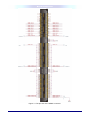
1
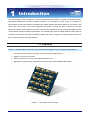
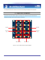
Terasic THDB-H2G
XTS
Terasic XTS Daughter Card
User Manual
Document Version 1.0
DEC. 29, 2009 by Terasic
Introduction
Page Index
INTRODUCTION ..............................................................................................................................................................................1
1-1 1.1 FEATURES .............................................................................................................................................................................1
1.2 ABOUT THE KIT............................................................................................................................................................................2
1-2 1.2 GETTING HELP ......................................................................................................................................................................2
ARCHITECTURE .............................................................................................................................................................................3
1-3 2.1 LAYOUT AND COMPONETS ....................................................................................................................................................3
1-4 2.2 BLOCK DIAGRAM ...................................................................................................................................................................5
BOARD COMPONENTS.................................................................................................................................................................6
1-5 3.1 HSMC EXPANSION CONNECTOR .........................................................................................................................................6
DEMONSTRATION........................................................................................................................................................................13
4.1 INTRODUCTION...........................................................................................................................................................................13
4.2 SYSTEM REQUIREMENTS ..........................................................................................................................................................14
4.3 SETUP THE DEMONSTRATION ....................................................................................................................................................14
4.4 DEMO OPERATION .....................................................................................................................................................................16
APPENDIX ......................................................................................................................................................................................17
5.1 REVISION HISTORY ....................................................................................................................................................................17
5.2 ALWAYS VISIT XTS W EBPAGE FOR NEW MAIN BOARD.............................................................................................................17
ii
Introduction
1
Introduction
The XTS daughter card is designed to convert FPGA transceiver channels to SMA connectors through a
High-Speed Mezzanine Connector (HSMC) interface. It is intended to allow users to evaluate the
performance of transceiver-based host boards with HMSC interface specifically Stratix IV GX, Stratix II GX,
Arria II GX, and Cyclone IV GX with integrated transceivers. Through the SMA connectors, the FPGA
transceiver signals can be easily connected to measurement instruments as well as allowing gigabit data rate
communication between multiple FPGA boards. The XTS daughter card is the ideal platform to allow users to
prototype and test their high-speed interfaces quickly and easily in support of transceiver performance for
jitter, protocol compliance, and equalization.
1.1 Features
1-1
Figure 1.1 shows the photo of the XTS card. The important functions of the XTS card are listed below:
•
Convert transceiver channels to SMA connectors through HSMC interface
•
Support 4 transceiver channels
•
SMA connectors for PLL input and output differential clock
•
Applicable for large volume applications that require high-speed (Gigabit) data transfer
Figure 1.1. The picture of the XTS card
1
Introduction
1.2 About the KIT
This section describes the package content
•
XTS Card x 1
•
System CD-ROM x 1
The CD contains technical documents of the XTS card
Figure 1.2 XTS Card Package
1.2 Getting Help
1-2
Here are some places to get help if you encounter any problem:
Email to [email protected]
Taiwan & China: +886-3-550-8800
Korea : +82-2-512-7661
Japan: +81-428-77-7000
2
Architecture
2
Architecture
This chapter describes the architecture of the XTS card including block diagram and components.
2.1 Layout and Componets
1-3
The picture of the XTS is shown in Figure 2.1 and Figure 2.2. It depicts the layout of the board and
indicates the locations of the connectors and key components.
TX SMAs
RX SMAs
Test-Point
Area
Test-Point
Area
SMA Output CLK
SMA Input CLK
Figure 2.1 The XTS Card PCB and component diagram
3
Architecture
Figure 2.2 The XTS card back side – HSMC connector view
The following components are provided on the XTS card :
•
HSMC expansion connector (J8)
•
TX SMAs (J9,J11,J13,J15,J17,J19,J21,J23)
•
RX SMAs (J10,J12,J14,J16,J18,J20,J22,J24)
•
SMA Output CLK (J25,J27)
•
SMA Input CLK (J26,J28)
4
Architecture
2.2 Block Diagram
1-4
Figure 2.3 shows the block diagram of the XTS card.
HSMC
Connector
Channel 1
Channel 2
4
Transceivers
4
Channel 3
Channel 4
Transceivers connected to SMA
connectors
Clock In/Out
Clock Inputs/Outputs to
SMA Connectors
Figure 2.3. The block diagram of the XTS Card
5
Board Components
3
Board Components
This section will describe the detailed information of the components, connector interfaces,
and the pin mappings on the XTS card.
3.1 HSMC Expansion Connector
1-5
This section describes the HSMC connector on the XTS card
The XTS card contains an Altera standard HSMC connector. All the other interfaces on the XTS card are
connected to the HSMC connector. Figure 3.1 shows the pin-outs of the HSMC connector and Table 3.1 lists
the description of each signals corresponding to the HSMC connector.
6
Board Components
Figure 3.1 The pin-outs of the HSMC connector.
7
Board Components
Table 3.1 below lists the HSMC signal direction and description
Pin
Name
Direction
Description
1
N.C.
N/A
Not Connect
2
N.C.
N/A
Not Connect
3
N.C.
N/A
Not Connect
4
N.C.
N/A
Not Connect
5
N.C.
N/A
Not Connect
6
N.C.
N/A
Not Connect
7
N.C.
N/A
Not Connect
8
N.C.
N/A
Not Connect
9
N.C.
N/A
Not Connect
10
N.C.
N/A
Not Connect
11
N.C.
N/A
Not Connect
12
N.C.
N/A
Not Connect
13
N.C.
N/A
Not Connect
14
N.C.
N/A
Not Connect
15
N.C.
N/A
Not Connect
16
N.C.
N/A
Not Connect
17
HSMC_TX_P3
Output
SMA Transceiver Output
18
HSMC_RX_P3
Input
SMA Transceiver Input
19
HSMC_TX_N3
Output
SMA Transceiver Output
20
HSMC_RX_N3
Input
SMA Transceiver Input
21
HSMC_TX_P2
Output
SMA Transceiver Output
22
HSMC_RX_P2
Input
SMA Transceiver Input
23
HSMC_TX_N2
Output
SMA Transceiver Output
24
HSMC_RX_N2
Input
SMA Transceiver Input
25
HSMC_TX_P1
Output
SMA Transceiver Output
26
HSMC_RX_P1
Input
SMA Transceiver Input
27
HSMC_TX_N1
Output
SMA Transceiver Output
28
HSMC_RX_N1
Input
SMA Transceiver Input
29
HSMC_TX_P0
Output
SMA Transceiver Output
30
HSMC_RX_P0
Input
SMA Transceiver Input
31
HSMC_TX_N0
Output
SMA Transceiver Output
32
HSMC_RX_N0
Input
SMA Transceiver Input
33
N.C.
N/A
Not Connect
34
N.C.
N/A
Not Connect
35
HSMC_TCK
Inout
JTAG
Numbers
8
Board Components
36
HSMC_TMS
Inout
JTAG
37
HSMC_TDO
Inout
JTAG
38
HSMC_TDI
Inout
JTAG
39
HSMC_CLKOUT0
N/A
CLKOUT0 Test-Point
40
HSMC_CLKIN0
N/A
CLKIN0 Test-Point
41
N.C.
N/A
Not Connect
42
N.C.
N/A
Not Connect
43
N.C.
N/A
Not Connect
44
N.C.
N/A
Not Connect
45
3V3
Power
Power 3.3V
46
12V
Power
Power 12V
47
N.C.
N/A
Not Connect
48
N.C.
N/A
Not Connect
49
N.C.
N/A
Not Connect
50
N.C.
N/A
Not Connect
51
3V3
Power
Power 3.3V
52
12V
Power
Power 12V
53
N.C.
N/A
Not Connect
54
N.C.
N/A
Not Connect
55
N.C.
N/A
Not Connect
56
N.C.
N/A
Not Connect
57
3V3
Power
Power 3.3V
58
12V
Power
Power 12V
59
N.C.
N/A
Not Connect
60
N.C.
N/A
Not Connect
61
N.C.
N/A
Not Connect
62
N.C.
N/A
Not Connect
63
3V3
Power
Power 3.3V
64
12V
Power
Power 12V
65
N.C.
N/A
Not Connect
66
N.C.
N/A
Not Connect
67
N.C.
N/A
Not Connect
68
N.C.
N/A
Not Connect
69
3V3
Power
Power 3.3V
70
12V
Power
Power 12V
71
N.C.
N/A
Not Connect
72
N.C.
N/A
Not Connect
73
N.C.
N/A
Not Connect
9
Board Components
74
N.C.
N/A
Not Connect
75
3V3
Power
Power 3.3V
76
12V
Power
Power 12V
77
N.C.
N/A
Not Connect
78
N.C.
N/A
Not Connect
79
N.C.
N/A
Not Connect
80
N.C.
N/A
Not Connect
81
3V3
Power
Power 3.3V
82
12V
Power
Power 12V
83
N.C.
N/A
Not Connect
84
N.C.
N/A
Not Connect
85
N.C.
N/A
Not Connect
86
N.C.
N/A
Not Connect
87
3V3
Power
Power 3.3V
88
12V
Power
Power 12V
89
N.C.
N/A
Not Connect
90
N.C.
N/A
Not Connect
91
N.C.
N/A
Not Connect
92
N.C.
N/A
Not Connect
93
3V3
Power
Power 3.3V
94
12V
Power
Power 12V
95
HSMC_CLKOUT_P1
N/A
Differential CLKOUT Test-Point
96
HSMC_CLKIN_P1.
N/A
Differential CLKIN Test-Point
97
HSMC_CLKOUT_N1
N/A
Differential CLKOUT Test-Point
98
HSMC_CLKIN_N1
N/A
Differential CLKIN Test-Point
99
3V3
Power
Power 3.3V
100
12V
Power
Power 12V
101
N.C.
N/A
Not Connect
102
N.C.
N/A
Not Connect
103
N.C.
N/A
Not Connect
104
N.C.
N/A
Not Connect
105
3V3
Power
Power 3.3V
106
12V
Power
Power 12V
107
N.C.
N/A
Not Connect
108
N.C.
N/A
Not Connect
109
N.C.
N/A
Not Connect
110
N.C.
N/A
Not Connect
111
3V3
Power
Power 3.3V
10
Board Components
112
12V
Power
Power 12V
113
N.C.
N/A
Not Connect
114
N.C.
N/A
Not Connect
115
N.C.
N/A
Not Connect
116
N.C.
N/A
Not Connect
117
3V3
Power
Power 3.3V
118
12V
Power
Power 12V
119
N.C.
N/A
Not Connect
120
N.C.
N/A
Not Connect
121
N.C.
N/A
Not Connect
122
N.C.
N/A
Not Connect
123
3V3
Power
Power 3.3V
124
12V
Power
Power 12V
125
N.C.
N/A
Not Connect
126
N.C.
N/A
Not Connect
127
N.C.
N/A
Not Connect
128
N.C.
N/A
Not Connect
129
3V3
Power
Power 3.3V
130
12V
Power
Power 12V
131
N.C.
N/A
Not Connect
132
N.C.
N/A
Not Connect
133
N.C.
N/A
Not Connect
134
N.C.
N/A
Not Connect
135
3V3
Power
Power 3.3V
136
12V
Power
Power 12V
137
N.C.
N/A
Not Connect
138
N.C.
N/A
Not Connect
139
N.C.
N/A
Not Connect
140
N.C.
N/A
Not Connect
141
3V3
Power
Power 3.3V
142
12V
Power
Power 12V
143
N.C.
N/A
Not Connect
144
N.C.
N/A
Not Connect
145
N.C.
N/A
Not Connect
146
N.C.
N/A
Not Connect
147
3V3
Power
Power 3.3V
148
12V
Power
Power 12V
149
N.C.
N/A
Not Connect
11
Board Components
150
N.C.
N/A
Not Connect
151
N.C.
N/A
Not Connect
152
N.C.
N/A
Not Connect
153
3V3
Power
Power 3.3V
154
12V
Power
Power 12V
155
HSMC_CLKOUT_P2
Output
SMA differential Output CLK
156
HSMC_CLKIN_P2
Input
SMA differential Input CLK
157
HSMC_CLKOUT_N2
Output
SMA differential Output CLK
158
HSMC_CLKIN_N2
Input
SMA differential Input CLK
159
3V3
Power
Power 3.3V
160
HSMC_PSNTn
Power
Power Ground
12
Demonstration
4
Demonstration
This chapter illustrates the reference design for the XTS HSMC card
4.1 Introduction
This section describes the functionality of the demonstration briefly.
The demonstration illustrates a loopback test for transceiver channels using the XTS daughter card and the
Stratix IV GX FPGA Development board. Figure 4.1 depicts the basic block diagram for this demonstration.
The demonstration is intended for users to provide a basic introduction to the XTS daughter card with the
procedures to control different hardware and software settings.
FPGA Host Board
XTS Board
HSMC Connector
TX
Transceiver
Channels
TX_Pattern
ALTGX
(Altera
Transceiver
Megafunction)
RX_Verify
TX
SMA Connector
SMA Cable
RX
Transceiver
Channels
RX
SMA Connector
Figure 4.1 Block diagram of the loopback test function
13
Demonstration
4.2 System Requirements
The following items are required for the XTS loopback demonstration.
•
XTS x 1
•
Stratix IV GX FPGA Development Board x 1
•
SMA Cable x 8
4.3 Setup the Demonstration
Figure 4.2, 4.3, 4.4 and 4.5 shows how to setup hardware for the XTS demonstration.
i.
Connect SMA Cable to J21 and J23 as shown in Figure 4.2 to short the positive signal of the
transceiver channel 0 (HSMC-TX0p).
Figure 4.2 Short J21 and J22 via SMA Cable
ii.
Connect SMA Cable to J22 and J24 as shown in Figure 4.3 to short the negative signal of the
transceiver channel 0 (HSMC-TX0n).
14
Demonstration
Figure 4.3 Short J23 and J24 via SMA Cable
iii.
Repeat steps i and ii to short the other transceiver channels as shown in Figure 4.4.
Figure 4.4 Short all the transceiver channels
iv.
Connect the XTS card to Stratix IV GX FPGA Development Board (See Figure 4.5).
15
Demonstration
Figure 4.5 Transceiver loopback test setup
Note: The XTS card must be connected to HSMC Slot “A” of the Stratix IV GX FPGA Development Board for
this demonstration
4.4 Demo Operation
This section describes the procedures of running the demonstration
FPGA Configuration
Demonstration Setup, File Locations, and Instructions
Transceiver Loopback Test Demo:
•
Project directory: xts_loopback_test_s4gfp
•
Bit Stream used: xts_loopback_test_s4gfp.sof
•
Stratix IV GX FPGA Development Kit Setup
•
Set SW4 switches 1, 2, 4 in the “up” position and switches 3, 5, 6, 8 in the “down” position
Set the rotary switch (SW2) to the 0 position
Power on the Stratix IV GX FPGA Development Board and download the SOF file
(xts_loopback_test_s4gfp.sof)
•
LED0~LED3 shows the test results for transceiver channels 0~3, respectively. If the LED is blinking, it
16
Appendix
indicates the test has passed.
•
Remove one of the SMA cable from one of the connector so that the loopback will fail.
indicated on the Stratix IV GX FPGA Dev Kit when the LED turns ON
•
To reset the board test system, press and release the PB0 reset button on the host board
•
Press and release PB1 can insert error pattern and create failure condition.
5
Appendix
5.1 Revision History
Date
Change Log
DEC 29, 2009
Initial Version
JAN 12, 2010
Added demonstration chapter
5.2 Always Visit XTS Webpage for New Main board
We will be continuing providing interesting examples and labs on our XTS
webpage. Please visit www.altera.com or xts.terasic.com for more information.
17
A Failure is