1
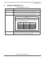
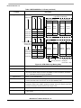
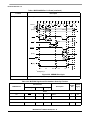
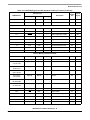
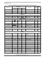
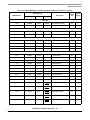
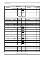
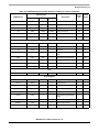
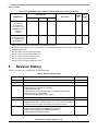
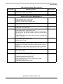
Freescale Semiconductor
User’s Manual Addendum
MCF5282UMAD
Rev. 15, 05/2007
MCF5282 User’s Manual Errata
by: Microcontroller Division
This errata document describes corrections to the
MCF5282 ColdFire Microcontroller User’s Manual,
order number MCF5282UM. For convenience, the
addenda items are grouped by revision. Please check our
website at http://www.freescale.com for the latest
updates.
© Freescale Semiconductor, Inc., 2007. All rights reserved.
Table of Contents
1
2
3
4
5
Errata for Revision 2.3 .........................................2
Errata for Revision 2.1 & 2.2 ...............................5
Errata for Revision 2.0 .........................................6
Errata for Revision 1.0 .........................................7
Revision History ................................................16
Errata for Revision 2.3
1
Errata for Revision 2.3
Table 1. MCF5282UM Rev 2.3 Errata
Location
Description
Table 2-1/Page 2-4
Remove last sentence in C bit field description.
Table 2-3/Page 2-7
Change PC’s Written with MOVEC entry to “No”.
Section 2.5/Page 2-8
Change last bullet to “Use of separate system stack pointers for user and supervisor
modes”
Section 2.5/Page 2-9
Change last sentence in fourth paragraph (step 2) to “The IACK cycle is mapped to special
locations within the interrupt controller's address space with the interrupt level encoded in
the address."
Figure 3-6/Page 3-8
Add minus sign to the exponent so that it is “–(i + 1 – N)”.
Table 4-3/Page 4-5
Change reset value of ACR0, ACR1 to “See Section” since some of the bits are undefined
after reset.
Figure 4-2/Page 4-6
Change CACR fields to R/W, since they may be read via the debug module.
Table 4-5/Page 4-8
For split instruction/data cache entry, swap text in parantheses in the description field.
Instruction cache uses the upper half of the arrays, while data cache uses the lower half.
Figure 4-3/Page 4-9
Change reset value of ACR: Bits 31-16, 14-13, 6-5, and 2 are undefined, and other bits are
cleared.
Change ACR fields to R/W, since they may be read via the debug module.
Section 4.4.2.2/Page 4-9
Change note to:
NOTE
Peripheral (IPSBAR) space should not be cached. The
combination of the CACR defaults and the two ACRn
registers must define the non-cacheable attribute for
this address space.
Figure 5-1/Page 5-2
Change RAMBAR fields to R/W, since they may be read via the debug module.
Table 5-1/Page 5-2
The PRI1/PRI2 text description does not match the table below it. It should be: “If a bit is
set, CPU has priority. If a bit is cleared, DMA has priority.”
Chapter 8
Remove any references to the core watchdog timer being able to reset the device. It is only
able to interrupt the processor. Use the peripheral watchdog timer described in
Chapter 18 if needing a watchdog timer to reset the device.
Table 9-4/Page 9-7
In the table for MFD bit definition, footnote (1) equation should read:
f ref × 2 ( MFD + 2 )
- ; f ref × 2 ( MFD + 2 ) ≤ f sys ( max ) ; fsys ≤ f sys ( max )
f sys = --------------------------------------------RFD
2
Where fsys(max) is the maximum system frequency for the particular MCF5282 device
(66MHz or 80MHz)
Section 10.3.6/Page 10-11 Include the following text in the section description and as a note in Figure 10-9.
“It is the responsibility of the software to program the ICRnx registers with unique and
non-overlapping level and priority definitions. Failure to program the ICRnx registers in
this manner can result in undefined behavior. If a specific interrupt request is completely
unused, the ICRnx value can remain in its reset (and disabled) state.”
Figure 10-6/Page 10-9
Interrupt Force Register Low (INTFRCLn) is illustrated as read-only in the figure. However,
this register should be read/write.
MCF5282 User’s Manual Errata, Rev. 15
2
Freescale Semiconductor
Errata for Revision 2.3
Table 1. MCF5282UM Rev 2.3 Errata (continued)
Location
Table 10-14/Page 10-15
Description
Change flag clearing mechanism for sources 24-26. They should read as follows:
Write ERR_INT = 1 after reading ERR_INT = 1
Write BOFF_INT = 1 after reading BOFF_INT = 1
Write WAKE_INT = 1 after reading WAKE_INT = 1
Table 12-7/Page 12-7
BAM bit field description, the first example should read “So, if CSAR0 = 0x0000 and
CSMR0[BAM] = 0x0001” instead of “So, if CSAR0 = 0x0000 and CSMR0[BAM] = 0x0008”.
Table 10-2/Page 10-4
In footnote, remove mention of the SWIACK register, as it is not supported in the global
IACK space.
Section 10.3.7/Page 10-16 Change last paragraph to: “In addition to the IACK registers within each interrupt controller,
there are global LnIACK registers. A read from one of the global LnIACK registers returns
the vector for the highest priority unmasked interrupt within a level for all interrupt
controllers. There is no global SWIACK register. However, reading the SWIACK register
from each interrupt controller returns the vector number of the highest priority unmasked
request within that controller.”
Table 15-1/Page 15-3
NOP command entry. Replace “SRAS asserted” with “SDRAM_CS[1:0] asserted”
Table 15-5/Page 15-7
Add the following note to the DACRn[CBM] field description:
Note: It is important to set CBM according to the location of the command bit.
Section 16.5/Page 16-11
Remove last sentence in this section starting with “BCRn decrements...” since SAA bit is
not supported.
Chapter 17
The maximum buffer size of the FEC is 2032 bytes. Replace any mention of the max size
being 2047 bytes with 2032 bytes.
Section 17.4.6/Page 17-7
Add the following subsection entitled “Duplicate Frame Transmission”:
The FEC fetches transmit buffer descriptors (TxBDs) and the corresponding transmit data
continuously until the transmit FIFO is full. It does not determine whether the TxBD to be
fetched is already being processed internally (as a result of a wrap). As the FEC nears the
end of the transmission of one frame, it begins to DMA the data for the next frame. In order
to remain one BD ahead of the DMA, it also fetches the TxBD for the next frame. It is
possible that the FEC will fetch from memory a BD that has already been processed but not
yet written back (that is, it is read a second time with the R bit still set). In this case, the data
is fetched and transmitted again.
Using at least three TxBDs fixes this problem for large frames, but not for small frames. To
ensure correct operation for either large or small frames, one of the following must be true:
• The FEC software driver ensures that there is always at least one TxBD with the ready
bit cleared.
• Every frame uses more than one TxBD and every TxBD but the last is written back
immediately after the data is fetched.
• The FEC software driver ensures a minimum frame size, n. The minimum number of
TxBDs is then (Tx FIFO Size ÷ (n + 4)) rounded up to the nearest integer (though the
result cannot be less than three). The default Tx FIFO size is 192 bytes; this size is
programmable.
Table 17-9/Page 17-17
Correct MIB block counters end addresses to IPSBAR + 0x12FF.
Table 17-11/Page 17-19
Add RMON_R_DROP with an IPSBAR Offset of 0x1280 and a description of ‘Count of
frames not counted correctly’.
Figure 17-26/Page 17-41
Change EMRBR register address from “IPSBAR + 0x11B8” to “IPSBAR + 0x1188”.
Section 20.5.13/Page 20-12 Deleted reference to nonexistent CF bits in the figure and bit descriptions for the GPTFLG2
register.
MCF5282 User’s Manual Errata, Rev. 15
Freescale Semiconductor
3
Errata for Revision 2.3
Table 1. MCF5282UM Rev 2.3 Errata (continued)
Location
Description
Figure 23-18/Page 23-18
Remove the two 16-bit divider blocks from timer input, as the divider is not available using
external clock sources.
Section 23.5.1.2.2/Page
23-19
Remove 16-bit divider from equation, as the divider is not available using external clock
sources.
Section 25.5.8/Page 25-25 Change end of last sentence from “...and can be written by the host to ‘0’.” to “...and can be
written by the host to ‘1’.”
Table 25-17/Page 25-29
Remove the following information from the BITERR and ACKERR descriptions as these
fields are read only: “To clear this bit, first read it as a one, then write it as a one. Writing
zero has no effect.” (This is a rescindment of a previous documentation errata.)
Change last sentence in ERRINT description from: “To clear this bit, first read it as a one,
then write as a zero. Writing a one has no effect.” to “To clear this bit, first read it as a
one, then write a one. Writing a zero has no effect.”
Add the following information to the BOFFINT and WAKEINT descriptions: “To clear this bit,
first read it as a one, then write it as a one. Writing zero has no effect.”
Table 25-17/Page 25-27
Definition of bits ERRINT and BOFFINT are incorrect for register ESTAT: ERRINT should
be bit 1, BOFFINT should be bit 2. They should be cleared by writing a one instead of a
zero.
Table 26-1/Page 26-5
Change description field for DTOUT1 from “DMA timer 1 output / Port TD[3]...” to “DMA
timer 1 output / Port TD[2]...”
Change description field for DTIN0 from “DMA timer 0 input / Port TD[3]...” to “DMA timer 1
output / Port TD[1]...”
Change description field for DTOUT0 from “DMA timer 0 output / Port TD[3]...” to “DMA
timer 1 output / Port TD[0]...”
Table 30-12/Page 30-14
Add the following note to the PBR[Address] field description:
Note: PBR[0] should always be loaded with a 0.
Table 30-20/Page 30-35
Change CSR’s initial state to 0x0000_0000.
Chapter 33
Add the following note:
“It is crucial during power-up that VDD never exceeds VDDH by more that ~0.3V. There
are diode devices between the two voltage domains, and violating this rule can lead to a
latch-up condition.”
Table 33-3/Page 33-3
In the VOH and VOL entries, change the respective IOH and IOL specs from “IOH = -2.0mA”
to “IOH = -5.0mA” and “IOL = +2.0mA” to “IOL = +5.0mA”
Table 33-8/Page 33-7
In the PLL Electrical Specifications table, only specs for the 80MHz MCF5282 device were
listed. Insert specs for the 66MHz device in the first 2 rows and also declare symbol
fsys(max), as shown below:
Max
Characteristic
Symbol
PLL Reference Frequency Range
Crystal reference
fref_crystal
fref_ext
External reference
1:1 Mode
fref_1:1
System Frequency 1
External Clock Mode
On-Chip PLL Frequency
Min
Unit
66MHz
80MHz
8.33
8.33
66.66
10.0
10.0
80
MHz
2
2
33.33
fsys
0
fref / 32
fsys(max) fsys(max) MHz
66.66
80
66.66
80
MCF5282 User’s Manual Errata, Rev. 15
4
Freescale Semiconductor
Errata for Revision 2.1 & 2.2
Table 1. MCF5282UM Rev 2.3 Errata (continued)
Location
Description
Table 33-8/Page 33-7
Change EXTAL Input High Voltage (VIHEXT) Crystal Mode minimum spec from “VDD - 1.0”
to “VXTAL + 0.4”.
Change EXTAL Input Low Voltage (VILEXT) Crystal Mode maximum spec from “1.0” to
“VXTAL - 0.4”.
Section 33.13.1/Page 33-21 Remove second sentence:
“There is no minimum frequency requirement.”
Section 33.13.2/Page 33-22 Remove second sentence:
“There is no minimum frequency requirement.”
Remove second paragraph as this feature is not supported on this device:
“The transmit outputs (ETXD[3:0], ETXEN, ETXER) can be programmed to
transition from either the rising or falling edge of ETXCLK, and the timing is the
same in either case. This options allows the use of non-compliant MII PHYs. Refer
to the Ethernet chapter for details of this option and how to enable it.”
Table A-3/Page A-4
2
The CSMR1 and CSCR1 register addresses are incorrect. They should be
IPSBAR + 0x090 and IPSBAR + 0x096 respectively
Errata for Revision 2.1 & 2.2
Table 2. MCF5282UM Rev 2.1 & 2.2 Errata
Location
Description
Figure 4-2/4-6
Changed bit 23 from DIDI to DISI
Table 4-6/4-9
Under ‘Configuration’ for ‘Instruction Cache’ the ‘Operation’ entry changed to “Invalidate
2 KByte data cache”
Table 4-6/4-9
Under ‘Configuration’ for ‘Data Cache’ the ‘Operation’ entry changed to “Invalidate 2 KByte
instruction cache”
Figure 6-3/6-6
Changed bit 8 to write-only instead of read/write
Table 6-10/6-15
Table 9-4/9-7
Removed “selected by BKSL[1:0]” as these are internal signal names not necessary for
end-user.
In the table for MFD bit definition, footnote (1) equation should read:
f ref × 2 ( MFD + 2 )
- ; f ref × 2 ( MFD + 2 ) ≤ f sys ( max ) ; fsys ≤ f sys ( max )
f sys = --------------------------------------------RFD
2
Where fsys(max) is the maximum system frequency for the particular MCF5282 device
(66MHz or 80MHz)
10.3.2/10-8
Add the following note: ‘If an interrupt source is being masked in the interrupt controller
mask register (IMR) or a module’s interrupt mask register while the interrupt mask in the
status register (SR[I]) is set to a value lower than the interrupt’s level, a spurious interrupt
may occur. This is because by the time the status register acknowledges this interrupt,
the interrupt has been masked. A spurious interrupt is generated because the CPU
cannot determine the interrupt source. To avoid this situation for interrupts sources with
levels 1-6, first write a higher level interrupt mask to the status register, before setting the
mask in the IMR or the module’s interrupt mask register. After the mask is set, return the
interrupt mask in the status register to its previous value. Since level seven interrupts
cannot be disabled in the status register prior to masking, use of the IMR or module
interrupt mask registers to disable level seven interrupts is not recommended.’
MCF5282 User’s Manual Errata, Rev. 15
Freescale Semiconductor
5
Errata for Revision 2.0
Table 2. MCF5282UM Rev 2.1 & 2.2 Errata (continued)
Location
Description
Chapter 17
The maximum buffer size of the FEC is 2032 bytes. Replace any mention of the max size
being 2047 bytes with 2032 bytes.
Table 17-2/17-5
Figure 17-23/17-39
25.4.10/25-16
In PALR/PAUR entry, delete “(only needed for full duplex flow control)”
Change FRSR to read/write instead of read-only.
Change CANICR to ICRn.
Table 25-17/25-29
Add the following information to BITERR and ACKERR descriptions: “To clear this bit, first
read it as a one, then write it as a one. Writing zero has no effect.”
Table 25-17/25-30
Change bit ordering: ERRINT should be bit 2 and BOFFINT should be bit 1.
Table 25-19/25-32
Change BUFnI field description from “To clear an interrupt flag, first read the flag as a one,
then write it as a zero” to “To clear an interrupt flag, first read the flag as a one, then write
it as a one.”
Chapter 33
It is crucial during power-up that VDD never exceeds VDDH by more that ~0.3V. There are
diode devices between the two voltage domains, and violating this rule can lead to a
latch-up condition.
Table 33-8/33-7
In the PLL Electrical Specifications table, only specs for the 80MHz MCF5282 device were
listed. Insert specs for the 66MHz device in the first 2 rows and also declare symbol
fsys(max), as shown below:
Max
Characteristic
Symbol
PLL Reference Frequency Range
Crystal reference
fref_crystal
External reference
fref_ext
1:1 Mode
fref_1:1
System Frequency 1
External Clock Mode
On-Chip PLL Frequency
3
Min
Unit
66MHz
80MHz
8.33
8.33
66.66
10.0
10.0
80
MHz
2
2
33.33
fsys
0
fref / 32
fsys(max) fsys(max) MHz
66.66
80
66.66
80
Errata for Revision 2.0
Table 3. MCF5282UM Rev 2.0 Errata
Location
Table 33-8/33-9
Description
Reference to ‘TA = TL to TH’ was not deleted. Delete.
MCF5282 User’s Manual Errata, Rev. 15
6
Freescale Semiconductor
Errata for Revision 1.0
4
Errata for Revision 1.0
Table 4. MCF5282UM Rev 1.0 Errata
Location
1.1/1-1
Description
Change ‘Real time debug support, with two user-visible hardware breakpoint registers’
To ‘Real time debug support, with one user-visible hardware breakpoint register’
Table 2-2/2-7
Change the I field description to read: “Interrupt level mask. Defines the current interrupt
level. Interrupt requests are inhibited for all priority levels less than or equal to the current
level, except the edge-sensitive level 7 request, which cannot be masked.”
Table 5-1/5-2
Replace the description of PRI1 and PRI2 with the following:
Description
Priority bit. PRI1 determines if DMA or CPU has priority in upper 32K bank of
memory. PRI2 determines if DMA or CPU has priority in lower 32K bank of
memory. If bit is set, DMA has priority. If bit is reset, CPU has priority. Priority is
determined according to the following table.
PRI[1:2]
Upper Bank
Priority
Lower Bank
Priority
00
01
10
11
DMA Accesses
DMA Accesses
CPU Accesses
CPU Accesses
DMA Accesses
CPU Accesses
DMA Accesses
CPU Accesses
NOTE: The Motorola-recommended setting for the priority bits is 00.
Table 5-1/5-3
Add the following note to the SPV bit description: “The BDE bit in the second RAMBAR
register must also be set to allow dual port access to the SRAM. For more information,
see Section 8.4.2, ‘Memory Base Address Register (RAMBAR).’”
MCF5282 User’s Manual Errata, Rev. 15
Freescale Semiconductor
7
Errata for Revision 1.0
Table 4. MCF5282UM Rev 1.0 Errata (continued)
Location
Figure 6-2/6-4
Description
Replace Figure 6-2, “CFM 512K Array Memory Map,” with the figure below.
Logical Block 1 (256 Kbytes)
0x0007 FFFF
Flash Physical Block 2
0x0004 000C
3H[1]
3L[1]
0x0004 0008
2H[1]
2L[1]
0x0004 0004
3H[0]
3L[0]
0x0004 0000
2H[0]
2L[0]
Flash Physical Block 3
2H[31]
2L[31]
3H[31]
3L[31]
Memory
Array 2H
Memory
Array 2L
Memory
Array 3H
Memory
Array 3L
2H[0]
2L[0]
3H[0]
3L[0]
0x0003 FFFF
Logical Block 0 (256 Kbytes)
Flash Physical Block 0
Configuration Field
(0x0000_0400–
0x0000_0417)
0x0000 000C
1H[1]
1L[1]
0x0000 0008
0H[1]
0L[1]
0x0000 0004
1H[1]
1L[1]
0x0000 0000
0H[0]
0L[0]
Flash Physical Block 1
0H[31]
0L[31]
1H[31]
1L[31]
Memory
Array 0H
Memory
Array 0L
Memory
Array 1H
Memory
Array 1L
0H[0]
0L[0]
1H[0]
1L[0]
Each memory array = 64 Kbytes
(16 bits wide × 32K)
Each physical block = 128 Kbytes
(32 bits wide × 32K)
Figure 6-2. CFM 512K Array Memory Map
Table 6-12/6-16
Change value for page erase verify command to 0x06.
Table 6-13/6-20
Change value for page erase verify command to 0x06.
Table 8-3/8-5
Add the following note the BDE bit description: “The SPV bit in the CPU’s RAMBAR must
also be set to allow dual port access to the SRAM. For more information, see Section
5.3.1, ‘SRAM Base Address Register (RAMBAR).’”
Figure 9-1/9-3
Remove ÷ 2 from CLKGEN block.
10.3.6/10-11
Add this text to the end of the first paragraph: “If a specific interrupt request is completely
unused, the ICRnx value can remain in its reset (and disabled) state.”
10.5/10-17
Add the following note: “The wakeup mask level taken from LPICR[6:4] is adjusted by
hardware to allow a level 7 IRQ to generate a wakeup. That is, the wakeup mask value
used by the interrupt controller must be in the range of 0–6.”
Figure 12-4/12-8
13.5/13-15
Change CSCRn to reflect that AA is set to ‘1’ at reset.
Remove final paragraph. The paragraph incorrectly states that the MCF5282 does not have
a bus monitor.
MCF5282 User’s Manual Errata, Rev. 15
8
Freescale Semiconductor
Errata for Revision 1.0
Table 4. MCF5282UM Rev 1.0 Errata (continued)
Location
Table 17-13/17-26
Description
Change encodings for bits 31–9 to:
0The corresponding interrupt source is masked.
1The corresponding interrupt source is not masked.
Chapter 19
Change PIT1–PIT4 to PIT0–PIT3 throughout chapter. When a timer is referenced
individually, PIT1 should be PIT0, PIT2 should be PIT1, PIT3 should be PIT2, and PIT4
should be PIT3. Other chapters in the user’s manual use the correct nomenclature:
PIT0–PIT3.
19.6.3/19-7
Change timeout period equation to the equation below.
PRE[3:0] × (PM[15:0] + 1) × 2
Timeout period = ----------------------------------------------------------------------------system clock
Figure 23-11
Change UISR bits 5–3 to reserved bits
24.6.1/24-11
Change ‘I2CR = 0xA’ to ‘I2CR = 0xA0.’
27.2.1/27-2
Change ‘When interfacing to 16-bit ports, the port C and D pins and PJ[7:6] (BS[3:2]) can
be configured as general-purpose input/output (I/O)’
To ‘When interfacing to 16-bit ports, the port C and D pins and PJ[5:4] (BS[1:0]) can be
configured as general-purpose input/output (I/O)’
32.2/32-7
Added additional device number order information to Table 32-2.
Table 32-2. Orderable Part Numbers
Motorola
Part Number
Description
MCF5280CVF66 MCF5280 RISC Microprocessor, 256 MAPBGA
MCF5280CVF80 MCF5280 RISC Microprocessor, 256 MAPBGA
MCF5281CVF66 MCF5281 RISC Microprocessor, 256 MAPBGA
MCF5281CVF80 MCF5281 RISC Microprocessor, 256 MAPBGA
MCF5282CVF66 MCF5282 RISC Microprocessor, 256 MAPBGA
MCF5282CVF80 MCF5282 RISC Microprocessor, 256 MAPBGA
Chapter 33
Speed
Temperature
66.67 MHz -40° to +85° C
80 MHz
-40° to +85° C
66.67 MHz -40° to +85° C
80 MHz
-40° to +85° C
66.67 MHz -40° to +85° C
80 MHz
-40° to +85° C
Delete references to ‘TA = TL to TH’.
Table 33-1/33-1
The Digital Input Voltage (VIN) absolute maximum rating should be -0.3 to 6.0 V
Table 33-6/33-8
The normal operation analog supply current (IDDA) maximum value has been changed to
5.0 mA.
MCF5282 User’s Manual Errata, Rev. 15
Freescale Semiconductor
9
Errata for Revision 1.0
Table 4. MCF5282UM Rev 1.0 Errata (continued)
Location
Description
Figure 33-5/33-16
Replace Figure 33-5, ‘SDRAM Read Cycle’ with the figure below.
0
1
2
3
4
5
6
7
8
9
10
11
12
13
CLKOUT
D3
D1
Row
A[23:0]
Column
D4
SRAS
D2
SCAS 1
D4
DRAMW
D5
D[31:0]
D6
SDRAM_CS[1:0]
D4
BS[3:0]
ACTV
NOP
NOP
READ
PRE
1 DACR[CASL] = 2
Figure 33-5. SDRAM Read Cycle
Table 14-3/14-11
Change ‘Internal Pull-Up’ column to pull-up indications in the table below.
Table 14-3. MCF5282 Signals and Pin Numbers Sorted by Function
Pin Functions
MAPBGA Pin
Description
Primary2
Secondary
Tertiary
Internal
Primary
Pull-up
I/O
1
Reset
R11
RSTI
—
—
Reset in
I
Yes
P11
RSTO
—
—
Reset out
O
—
External clock/crystal in
I
—
Clock
T8
EXTAL
—
—
MCF5282 User’s Manual Errata, Rev. 15
10
Freescale Semiconductor
Errata for Revision 1.0
Table 14-3. MCF5282 Signals and Pin Numbers Sorted by Function (continued)
Pin Functions
MAPBGA Pin
Description
Internal
Primary
Pull-up
I/O
1
Primary2
Secondary
Tertiary
R8
XTAL
—
—
Crystal drive
O
—
N7
CLKOUT
—
—
Clock out
O
—
Chip Configuration/Mode Selection
R14
CLKMOD0
—
—
Clock mode select
I
Yes
T14
CLKMOD1
—
—
Clock mode select
I
Yes
T11
RCON
—
—
Reset configuration enable
I
Yes
H1
D26
PA2
—
Chip mode
I/O
—
K2
D17
PB1
—
Chip mode
I/O
—
K3
D16
PB0
—
Chip mode
I/O
—
J4
D19
PB3
—
Boot device/data port size
I/O
—
K1
D18
PB2
—
Boot device/data port size
I/O
—
J2
D21
PB5
—
Output pad drive strength
I/O
—
External Memory Interface and Ports
C6:B6:A5
A[23:21]
PF[7:5]
CS[6:4]
Address bus
O
Yes
C4:B4:A4:B3:A3
A[20:16]
PF[4:0]
—
Address bus
O
Yes
A2:B1:B2:C1:
C2:C3:D1:D2
A[15:8]
PG[7:0]
—
Address bus
O
Yes
D3:D4:E1:E2:
E3:E4:F1:F2
A[7:0]
PH[7:0]
—
Address bus
O
Yes
F3:G1:G2:G3:
G4:H1:H2:H3
D[31:24]
PA[7:0]
—
Data bus
I/O
—
H4:J1:J2:J3:
J4:K1:K2:K3
D[23:16]
PB[7:0]
—
Data bus
I/O
—
L1:L2:L3:L4:
M1:M2:M3:M4
D[15:8]
PC[7:0]
—
Data bus
I/O
—
N1:N2:N3:P1:
N5:T6:R6:P6
D[7:0]
PD[7:0]
—
Data bus
I/O
—
P14:T15:R15:R16
BS[3:0]
PJ[7:4]
—
Byte strobe
I/O
Yes
N16
OE
PE7
—
Output enable
I/O
—
P16
TA
PE6
—
Transfer acknowledge
I/O
Yes
P15
TEA
PE5
—
Transfer error acknowledge
I/O
Yes
N15
R/W
PE4
—
Read/write
I/O
Yes
N14
SIZ1
PE3
SYNCA
Transfer size
I/O
Yes3
MCF5282 User’s Manual Errata, Rev. 15
Freescale Semiconductor
11
Errata for Revision 1.0
Table 14-3. MCF5282 Signals and Pin Numbers Sorted by Function (continued)
Pin Functions
MAPBGA Pin
Internal
Primary
Pull-up
I/O
1
Description
Primary2
Secondary
Tertiary
M16
SIZ0
PE2
SYNCB
Transfer size
I/O
Yes4
M15
TS
PE1
SYNCA
Transfer start
I/O
Yes
M14
TIP
PE0
SYNCB
Transfer in progress
I/O
Yes
Chip Selects
L16:L15:L14:L13
CS[3:0]
PJ[3:0]
—
Chip selects 3-0
I/O
Yes
C6:B6:A5
A[23:21]
PF[7:5]
CS[6:4]
Chip selects 6-4
O
Yes
SDRAM Controller
H15
SRAS
PSD5
—
SDRAM row address strobe
I/O
—
H16
SCAS
PSD4
—
SDRAM column
address strobe
I/O
—
G15
DRAMW
PSD3
—
SDRAM write enable
I/O
—
H13:G16
SDRAM_CS[1:0]
PSD[2:1]
—
SDRAM chip selects
I/O
—
H14
SCKE
PSD0
—
SDRAM clock enable
I/O
—
External interrupt request
I/O
—
External Interrupts Port
B15:B16:C14:C15:
C16: D14:D15
IRQ[7:1]
PNQ[7:1]
—
Ethernet
C10
EMDIO
PAS5
URXD2
Management channel
serial data
I/O
—
B10
EMDC
PAS4
UTXD2
Management channel clock
I/O
—
A8
ETXCLK
PEH7
—
MAC Transmit clock
I/O
—
D6
ETXEN
PEH6
—
MAC Transmit enable
I/O
—
D7
ETXD0
PEH5
—
MAC Transmit data
I/O
—
B11
ECOL
PEH4
—
MAC Collision
I/O
—
A10
ERXCLK
PEH3
—
MAC Receive clock
I/O
—
C8
ERXDV
PEH2
—
MAC Receive enable
I/O
—
D9
ERXD0
PEH1
—
MAC Receive data
I/O
—
A11
ECRS
PEH0
—
MAC Carrier sense
I/O
—
A7:B7:C7
ETXD[3:1]
PEL[7:5]
—
MAC Transmit data
I/O
—
D10
ETXER
PEL4
—
MAC Transmit error
I/O
—
A9:B9:C9
ERXD[3:1]
PEL[3:1]
—
MAC Receive data
I/O
—
B8
ERXER
PEL0
—
MAC Receive error
I/O
—
MCF5282 User’s Manual Errata, Rev. 15
12
Freescale Semiconductor
Errata for Revision 1.0
Table 14-3. MCF5282 Signals and Pin Numbers Sorted by Function (continued)
Pin Functions
MAPBGA Pin
Description
Primary2
Secondary
Tertiary
Internal
Primary
Pull-up
I/O
1
FlexCAN
D16
CANRX
PAS3
URXD2
FlexCAN Receive data
I/O
—
E13
CANTX
PAS2
UTXD2
FlexCAN Transmit data
I/O
—
I2C
E14
SDA
PAS1
URXD2
I2C Serial data
I/O
Yes5
E15
SCL
PAS0
UTXD2
I2C Serial clock
I/O
Yes6
QSPI
F13
QSPI_DOUT
PQS0
—
QSPI data out
I/O
—
E16
QSPI_DIN
PQS1
—
QSPI data in
I/O
—
F14
QSPI_CLK
PQS2
—
QSPI clock
I/O
—
G14:G13:F16:F15
QSPI_CS[3:0]
PQS[6:3]
—
QSPI chip select
I/O
—
UARTs
R7
URXD1
PUA3
—
U1 receive data
I/O
—
P7
UTXD1
PUA2
—
U1 transmit data
I/O
—
N6
URXD0
PUA1
—
U0 receive data
I/O
—
T7
UTXD0
PUA0
—
U0 transmit data
I/O
—
C10
EMDIO
PAS5
URXD2
U2 receive data
I/O
—
B10
EMDC
PAS4
UTXD2
U2 transmit data
I/O
—
D16
CANRX
PAS3
URXD2
U2 receive data
I/O
—
E13
CANTX
PAS2
UTXD2
U2 transmit data
I/O
—
E14
SDA
PAS1
URXD2
U2 receive data
I/O
Yes5
E15
SCL
PAS0
UTXD2
U2 transmit data
I/O
Yes6
K16
DTIN3
PTC3
URTS1/
URTS0
U1/U0 Request to Send
I/O
—
K15
DTOUT3
PTC2
URTS1/
URTS0
U1/U0 Request to Send
I/O
—
K14
DTIN2
PTC1
UCTS1/
UCTS0
U1/U0 Clear to Send
I/O
—
K13
DTOUT2
PTC0
UCTS1/
UCTS0
U1/U0 Clear to Send
I/O
—
J16
DTIN1
PTD3
URTS1/
URTS0
U1/U0 Request to Send
I/O
—
MCF5282 User’s Manual Errata, Rev. 15
Freescale Semiconductor
13
Errata for Revision 1.0
Table 14-3. MCF5282 Signals and Pin Numbers Sorted by Function (continued)
Pin Functions
MAPBGA Pin
Internal
Primary
Pull-up
I/O
1
Description
Primary2
Secondary
Tertiary
J15
DTOUT1
PTD2
URTS1/
URTS0
U1/U0 Request to Send
I/O
—
J14
DTIN0
PTD1
UCTS1/
UCTS0
U1/U0 Clear to Send
I/O
—
J13
DTOUT0
PTD0
UCTS1/
UCTS0
U1/U0 Clear to Send
I/O
—
General Purpose Timers
T13:R13:P13:N13
GPTA[3:0]
PTA[3:0]
—
Timer A IC/OC/PAI
I/O
Yes
T12:R12:P12:N12
GPTB[3:0]
PTB[3:0]
—
Timer B IC/OC/PAI
I/O
Yes
N14
SIZ1
PE3
SYNCA
Timer A synchronization input
I/O
Yes3
M16
SIZ0
PE2
SYNCB
Timer B synchronization input
I/O
Yes4
M15
TS
PE1
SYNCA
Timer A synchronization input
I/O
Yes
M14
TIP
PE0
SYNCB
Timer B synchronization input
I/O
Yes
DMA Timers
K16
DTIN3
PTC3
URTS1/
URTS0
Timer 3 in
I/O
—
K15
DTOUT3
PTC2
URTS1/
URTS0
Timer 3 out
I/O
—
K14
DTIN2
PTC1
UCTS1/
UCTS0
Timer 2 in
I/O
—
K13
DTOUT2
PTC0
UCTS1/
UCTS0
Timer 2 out
I/O
—
J16
DTIN1
PTD3
URTS1/
URTS0
Timer 1 in
I/O
—
J15
DTOUT1
PTD2
URTS1/
URTS0
Timer 1 out
I/O
—
J14
DTIN0
PTD1
UCTS1/
UCTS0
Timer 0 in
I/O
—
J13
DTOUT0
PTD0
UCTS1/
UCTS0
Timer 0 out
I/O
—
Queued Analog-to-Digital Converter (QADC)
T3
AN0
PQB0
ANW
Analog channel 0
I/O
—
R2
AN1
PQB1
ANX
Analog channel 1
I/O
—
T2
AN2
PQB2
ANY
Analog channel 2
I/O
—
R1
AN3
PQB3
ANZ
Analog channel 3
I/O
—
MCF5282 User’s Manual Errata, Rev. 15
14
Freescale Semiconductor
Errata for Revision 1.0
Table 14-3. MCF5282 Signals and Pin Numbers Sorted by Function (continued)
Pin Functions
MAPBGA Pin
Description
Internal
Primary
Pull-up
I/O
1
Primary2
Secondary
Tertiary
R4
AN52
PQA0
MA0
Analog channel 52
I/O
—
T4
AN53
PQA1
MA1
Analog channel 53
I/O
—
P3
AN55
PQA3
ETRIG1
Analog channel 55
I/O
—
R3
AN56
PQA4
ETRIG2
Analog channel 56
I/O
—
P4
VRH
—
—
High analog reference
I
—
T5
VRL
—
—
Low analog reference
I
—
Debug and JTAG Test Port Control
R9
JTAG_EN
—
—
JTAG Enable
I
—
P9
DSCLK
TRST
—
Debug clock / TAP reset
I
Yes7
T9
TCLK
—
—
TAP clock
I
Yes7
P10
BKPT
TMS
—
Breakpoint/TAP test mode
select
I
Yes7
R10
DSI
TDI
—
Debug data in / TAP data in
I
Yes7
T10
DSO
TDO
—
Debug data out / TAP data out
O
—
C12:D12:A13:B13
DDATA[3:0]
PDD[7:4]
—
Debug data
I/O
—
C13:A14:B14:A15
PST[3:0]
PDD[3:0]
—
Processor status data
I/O
—
Test mode pin
I
—
Test
N10
TEST
—
Power Supplies
R5
VDDA
—
—
Analog positive supply
I
—
P5:T1
VSSA
—
—
Analog ground
I
—
P2
VDDH
—
—
ESD positive supply
I
—
N8
VDDPLL
—
—
PLL positive supply
I
—
P8
VSSPLL
—
—
PLL ground
I
—
A6:C11
VPP
—
—
Flash (stress) programming
voltage
I
—
A12:C5:D5:D11
VDDF
—
—
Flash positive supply
I
—
B5:B12:
VSSF
—
—
Flash module ground
I
—
N11
VSTBY
—
—
Standby power
I
—
MCF5282 User’s Manual Errata, Rev. 15
Freescale Semiconductor
15
Revision History
Table 14-3. MCF5282 Signals and Pin Numbers Sorted by Function (continued)
Pin Functions
MAPBGA Pin
Description
Internal
Primary
Pull-up
I/O
1
Primary2
Secondary
Tertiary
E6-E11:F5:F7-F10:
F12:G5:G6:G11:
G12:H5:H6:H11:
H12:J5:J6:J11:J12:
K5:K6:K11:K12:L5:
L7-L10:L12:
M6-M11
VDD
—
—
Positive supply
I
—
A1:A16:E5:E12:F6:
F11:G7-G10:H7-H10:
J7-J10:K7-K10:L6:
L11:M5:M12:T16
VSS
—
—
Ground
I
—
NOTES:
1
Pull-ups are not active when GPIO functions are selected for the pins.
2 The primary functionality of a pin is not necessarily its default functionality. Pins that have GPIO functionality will
default to GPIO inputs.
3 Pull-up is active only with the SYNCA function.
4 Pull-up is active only with the SYNCB function.
5 Pull-up is active only with the SDA function.
6 Pull-up is active only with SCL function.
7 Pull-up is active when JTAG_EN is driven high.
5
Revision History
Table 5 provides a revision history for this document.
Table 5. Revision History Table
Rev. Number
Substantive Changes
Date of Release
0
Initial release.
07/2003
1
Added page erase verify errata for Chapter 6, “ColdFire Flash Module (CFM).”
09/2003
2
•
•
•
•
Added errata for UART interrupt status register.
Added errata for PIT timer timeout equation.
Added I2CR write errata.
Added errata for ‘Internal Pull-Up’ column in ‘MCF5282 Signals and Pin
Numbers Sorted by Function’ table.
• Added errata for “SDRAM Read Cycle’ figure.
11/2003
3
• Added errata for Chapter 19. PIT1–PIT4 should be PIT0–PIT3.
01/2004
4
• Added errata for spurious interrupt.
• Added errata for Table 33-8. Single instance of TA = TL to TH was overlooked
in revision 2.0 of the manual. This instance has now been removed.
03/2004
5
•
•
•
•
03/2004
Added errata for Section 25.4.10: change CANICR to ICRn.
Added errata for BITERR and ACKERR field descriptions.
Added errata for BOFFINT and ERRINT bit sequence.
Added errata for BUFnI field description.
MCF5282 User’s Manual Errata, Rev. 15
16
Freescale Semiconductor
Revision History
Table 5. Revision History Table (continued)
Rev. Number
Substantive Changes
Date of Release
6
• Added errata for Table 17-2
• Added errata for FRSR register diagram
11/2004
7
• Added errata for Figure 4-2, Table 4-6, Figure 6-3, and Table 6-10
11/2004
Added the below errata for MCF5282UM Rev 2.3
Added FEC max buffer size errata.
Added VDD/VDDH power-up requirement.
Added MFD bit definition footnote errata.
Added PLL spec table entries for 66MHz device.
01/2005
8
•
•
•
•
9
• Added INTFRCLn figure errata.
• Added BAM bit field example errata.
03/2005
10
• Added SDRAM NOP command errata.
• Added UART clock source errata.
07/2005
11
• Added PRI1/PRI2 text description errata.
• Added CSMR1/CSCR1 register address errata.
• Removed Table 23-5 errata that was added in revision 10 of this document,
as it was incorrect. Only the internal UART clock source is prescaled by the
16-bit divider.
• Added 2 UART external clock source errata, removing the 16-bit divider from
a figure and equation.
08/2005
12
• Added core watchdog unable to reset the device errata.
• Added EMRBR register address errata.
• Added IOH and IOL errata.
12/2005
13
• Added FlexCAN flag clearing mechanism errata in interrupt controller.
• Added FlexCAN ESTAT register description errata for various bits.
• Added ICRnx note regarding unique and non-overlapping level and priority
definitions.
• Added DTOUT1, DTIN0, DTOUT0 description field errata in GPIO chapter.
• Added FEC MII transmit and receive specification section errata.
08/2006
14
• Deleted reference to nonexistent CF bits in the figure and bit descriptions for
the GPTFLG2 register.
• Added RMON_R_DROP counter errata.
11/2006
15
•
•
•
•
•
•
•
05/2007
Added various core, EMAC, cache, SRAM and debug chapter errata.
Added VIH and VIL crystal mode spec changes.
Added DACRn[CBM] field description note.
Added FEC MIB counter memory map errata.
Added “Duplicate Frame Transmission” section to FEC chapter.
Added DMA SAA bit errata.
Added global IACK register space errata.
MCF5282 User’s Manual Errata, Rev. 15
Freescale Semiconductor
17
How to Reach Us:
Home Page:
www.freescale.com
E-mail:
[email protected]
USA/Europe or Locations Not Listed:
Freescale Semiconductor
Technical Information Center, CH370
1300 N. Alma School Road
Chandler, Arizona 85224
+1-800-521-6274 or +1-480-768-2130
[email protected]
Europe, Middle East, and Africa:
Freescale Halbleiter Deutschland GmbH
Technical Information Center
Schatzbogen 7
81829 Muenchen, Germany
+44 1296 380 456 (English)
+46 8 52200080 (English)
+49 89 92103 559 (German)
+33 1 69 35 48 48 (French)
[email protected]
Japan:
Freescale Semiconductor Japan Ltd.
Headquarters
ARCO Tower 15F
1-8-1, Shimo-Meguro, Meguro-ku,
Tokyo 153-0064, Japan
0120 191014 or +81 3 5437 9125
[email protected]
Asia/Pacific:
Freescale Semiconductor Hong Kong Ltd.
Technical Information Center
2 Dai King Street
Tai Po Industrial Estate
Tai Po, N.T., Hong Kong
+800 2666 8080
[email protected]
For Literature Requests Only:
Freescale Semiconductor Literature Distribution Center
P.O. Box 5405
Denver, Colorado 80217
1-800-441-2447 or 303-675-2140
Fax: 303-675-2150
[email protected]
Information in this document is provided solely to enable system and
software implementers to use Freescale Semiconductor products. There are
no express or implied copyright licenses granted hereunder to design or
fabricate any integrated circuits or integrated circuits based on the
information in this document.
Freescale Semiconductor reserves the right to make changes without further
notice to any products herein. Freescale Semiconductor makes no warranty,
representation or guarantee regarding the suitability of its products for any
particular purpose, nor does Freescale Semiconductor assume any liability
arising out of the application or use of any product or circuit, and specifically
disclaims any and all liability, including without limitation consequential or
incidental damages. “Typical” parameters that may be provided in Freescale
Semiconductor data sheets and/or specifications can and do vary in different
applications and actual performance may vary over time. All operating
parameters, including “Typicals”, must be validated for each customer
application by customer’s technical experts. Freescale Semiconductor does
not convey any license under its patent rights nor the rights of others.
Freescale Semiconductor products are not designed, intended, or authorized
for use as components in systems intended for surgical implant into the body,
or other applications intended to support or sustain life, or for any other
application in which the failure of the Freescale Semiconductor product could
create a situation where personal injury or death may occur. Should Buyer
purchase or use Freescale Semiconductor products for any such unintended
or unauthorized application, Buyer shall indemnify and hold Freescale
Semiconductor and its officers, employees, subsidiaries, affiliates, and
distributors harmless against all claims, costs, damages, and expenses, and
reasonable attorney fees arising out of, directly or indirectly, any claim of
personal injury or death associated with such unintended or unauthorized
use, even if such claim alleges that Freescale Semiconductor was negligent
regarding the design or manufacture of the part.
Freescale™ and the Freescale logo are trademarks of Freescale
Semiconductor, Inc. All other product or service names are the property
of their respective owners.© Freescale Semiconductor, Inc. 2007. All rights
reserved.
MCF5282UMAD
Rev. 15
05/2007