1
A Global-Local Optimization Framework for Simultaneous
Multi-Mode Multi-Corner Clock Skew Variation Reduction
Kwangsoo Han‡ , Andrew B. Kahng†‡ , Jongpil Lee∗ , Jiajia Li‡ and Siddhartha Nath†
† CSE and ‡ ECE Departments, UC San Diego, ∗ Samsung Electronics Co. Ltd.
{kwhan, abk, jil150, sinath}@ucsd.edu, [email protected]
ABSTRACT
As combinations of signoff corners grow in modern SoCs,
minimization of clock skew variation across corners is important.
Large skew variation can cause difficulties in multi-corner timing
closure because fixing violations at one corner can lead to
violations at other corners.
Such “ping-pong” effects lead
to significant power and area overheads and time to signoff.
We propose a novel framework encompassing both global
and local clock network optimizations to minimize the sum
of skew variations across different PVT corners between all
sequentially adjacent sink pairs. The global optimization uses
linear programming to guide buffer insertion, buffer removal and
routing detours. The local optimization is based on machine
learning-based predictors of latency change; these are used for
iterative optimization with tree surgery, buffer sizing and buffer
displacement operators. Our optimization achieves up to 22% total
skew variation reduction across multiple testcases implemented in
foundry 28nm technology, as compared to a best-practices CTS
solution using a leading commercial tool.
Categories and Subject Descriptors
B.7.2 [Hardware]: INTEGRATED CIRCUITS—Design Aids
General Terms
Algorithms, Design, Optimization
1.
INTRODUCTION
Modern SoCs typically exploit complex operating scenarios
to maximize performance and reduce power consumption. For
instance, techniques such as dynamic voltage and frequency scaling
(DVFS), split rail power supply, etc. are widely applied in SoC
designs to meet performance and power targets. However, these
techniques increase the number of modes and corners used for
timing closure, which will in turn lead to increased datapath
delay variation and clock skew variation across corners. Such
large timing variations increase area and power overheads, as
well as design turnaround time (TAT) due to a “ping-pong” effect
whereby fixing timing issues at one corner leads to violations
at other corners. To solve this issue, we can minimize either
datapath delay variation or clock skew variation across corners.
Given that datapath optimization is a local optimization and is
usually applied after the clock network optimization, what datapath
delay variation minimization can accomplish is limited. In other
words, datapath optimizations are practically less impactful than
minimizing clock skew variations in most cases. This is why
clock network optimization is a key first step during the physical
implementation flow for timing closure. Further, clock skew
variation can be achieved via both global and local optimizations
of the clock network. Therefore, minimizing clock skew variation
across corners is more effective for multi-corner timing closure. In
this work, we minimize clock skew variation.
Moreover, timing violations due to clock skew variation across
corners are typically reduced by (hold and/or setup) buffer
insertion, Vth -swapping and gate sizing on datapaths at later
Permission to make digital or hard copies of all or part of this work for personal or
classroom use is granted without fee provided that copies are not made or distributed
for profit or commercial advantage and that copies bear this notice and the full citation
on the first page. Copyrights for components of this work owned by others than
ACM must be honored. Abstracting with credit is permitted. To copy otherwise, or
republish, to post on servers or to redistribute to lists, requires prior specific permission
and/or a fee. Request permissions from [email protected].
DAC’15, June 07 - 11 2015, San Francisco, CA, USA.
Copyright 2015 ACM 978-1-4503-3520-1/15/06 ...$15.00.
http://dx.doi.org/10.1145/2744769.2744776.
design stages. Thus, clock skew variation between each pair of
sequentially adjacent sinks can lead to potential costs of area,
power and design TAT. We therefore minimize the sum of skew
variations between all sink pairs to minimize the overall physical
implementation costs (e.g., in area, power, TAT).
Although many commercial EDA tools are capable of multimode multi-corner clock network synthesis [21] [25], our
optimization framework can be applied as an incremental
optimization for further reduction of skew variations in light of
our robust interface to commercial P&R and STA tools. Moreover,
experimental results show that our proposed optimization is able to
achieve significant skew variation reduction on clock networks that
have been synthesized with a leading commercial tool.
Contributions of our work are as follows.
1. We are the first in the literature to study the problem of
minimizing the sum of clock skew variations across multiple
PVT corners.
2. We propose a novel global-local framework for clock
network optimizations to minimize the sum, over all pairs
of PVT corners, of skew variation between all sequentially
adjacent pairs.
3. We demonstrate that machine learning-based predictors of
latency change can provide accurate guidance on the best
moves to test during local optimization for minimization of
skew variation across corners.
4. Our optimization framework has a robust interface to
leading commercial P&R and STA tools and production
PDKs/libraries, and can be generalized to other clock
network optimization problems.
5. We achieve up to 22% reduction in the sum of skew
variations of clock trees in testcases that reflect high-speed
application processor and memory controller blocks.
2.
RELATED WORK
We classify previous works on clock skew optimization as (i)
works that target skew and/or delay optimization at single or
multiple corners, and (ii) works that optimize skew variation across
multiple PVT corners.
Several previous works optimize skew at one or more PVT
corners, but do not address skew variation across corners. Cao
et al. [4] minimize the worst skew in a clock tree by partitioning
the tree into different skew groups. The authors then greedily
minimize the worst skew in each skew group to minimize overall
local skew. Cho et al. [6] perform clock tree optimization that
is temperature-aware. The authors modify the deferred merge
embedding (DME) algorithm to include merging diamonds for
consideration of temperature variations to guide clock skew and
wirelength minimization. Lung et al. [10] perform multi-mode
multi-corner (MMMC) clock skew optimization by minimizing the
worst skew across all corners. They propose a methodology to
determine the delay correlation factor for clock buffers at 130nm,
90nm and 65nm and conclude that the correlation across corners
is linear. However, such an assumption might not be valid at
28nm and below. Lung et al. [11] perform chip-level as well
as module-level clock skew optimizations with multiple voltage
modes. The authors use power-mode-aware buffers for chip-level
clock tree optimization. For the module-level optimization, they
only consider the worst voltage corner.
Relatively fewer works exist that optimize skew variation across
multiple PVT corners. Restle et al. [18] propose a two-dimensional
nontree structure. They divide the nontree structure into two levels
– leaf level (close to clock sinks) and top level (close to clock
source). The top level is the same as the traditional clock tree
structure, but the leaf level is a mesh structure such that each sink
is connected to the nearest point on the mesh. Although this is
a very effective way to minimize skew variation across corners,
the mesh structure consumes enormous wire resources and power.
Su and Sapatnekar [20] use mesh structures for the top-level tree
which consumes less wire resource and power as compared to [18].
However, this consumes 59%-168% more wire resource than a tree
structure. Further, the authors do not optimize skew variation which
still exists in the bottom-level subtrees. Rajaram et al. [16] [17]
propose a nontree construction method to insert crosslinks1 in a
clock tree by estimating subtree delays using the Elmore delay
model. The authors verify their method with SPICE-based Monte
Carlo simulations and report skew variability reduction. However,
the approach consumes excess additional wire and power due to
crosslink insertions. Mittal and Koh [15] propose a greedy method
to insert crosslinks to reduce skew variation.
To our knowledge, there has been no systematic framework
for minimization of clock skew variation (across multiple signoff
corners) for clock trees. Our work exploits both global and local
iterative optimizations to minimize skew variations across different
PVT corners which is very important for high-speed processor and
multimedia blocks that operate at multiple modes/corners. Further,
instead of minimizing the maximum skew or skew variation, we
minimize the sum of skew variations over all sink pairs, which will
reduce the potential costs of gate sizing and buffer insertion for
multi-corner timing closure.
3.
4.
Figure 1: Overview of our optimization framework.
PROBLEM FORMULATION
The notations we use in this paper are given in Table 1.
4.1
Table 1: Description of notations used in our work.
Term
ck
αk
fi
Pi
c
skewi,ik0
Meaning
operating corner, (0 ≤ k ≤ K; c0 is the nominal corner)
normalization factor of corner ck with respect to c0
sink (e.g., flip-flop) in clock tree, (1 ≤ i ≤ N)
clock path from clock source to fi
clock skew between sink pair ( fi , fi0 ) at corner ck
sj
c
D jk
ck
∆j
ck
Dmax
ck ,ck0
vi,i0
arc (i.e., tree segment without branching) in clock tree, (1 ≤ j ≤ M)
original arc delay at corner ck
delay change of arc s j at corner ck from optimization
maximum latency of a clock path at corner ck
normalized skew variation across corner pair (ck , ck0 ) between ( fi , fi0 )
Vi,i0
worst normalized skew variation across all corner pairs between ( fi , fi0 )
For a corner pair (ck , ck0 ), we define the normalized skew
variation between sink pair ( fi , fi0 ) as
c ,ck0
c
= |αk · skewci,ik 0 − αk0 · skewi,ik 0 |
vi,ik 0
0
(1)
where skew
is defined as the latency difference between
capture and launch clock paths at ck . We emphasize that our
optimization is local skew-aware, so that we only optimize skews
between launch-capture sink pairs that have valid datapaths in
between them (i.e., we avoid the pessimism that would result from
use of global skew in the formulation). αk is the normalization
factor at corner ck with respect to the nominal corner. Note that
αk is an input parameter and can be determined by technology
information (e.g., ratio between buffer delays at ck and c0 ), clock
tree properties (e.g., Vth and sizes of buffers in the tree), etc.
Further, one can define specific αk values for each sink pair. In
our work, we define αk as the average skew ratio between c0 and
ck over all sink pairs.
We further define the maximum skew variation across corners,
for each sink pair ( fi , fi0 ), as
c ,ck0
∀(ck ,ck0 )
Global Optimization
We construct a linear program (LP) to reduce the sum of skew
variations between all sink pairs in a clock tree. Based on the
LP solution, we determine the desired delay changes of arcs at
all corners and perform buffer insertion and removal, as well as
routing detour, to accomplish the desired delay changes. We
determine number of buffers, buffer size and length of routing
detour based on lookup tables. However, the achievable delay
values are discrete due to the limited number of buffer sizes.
Further, placement legalization and routing congestion also lead to
discrepancy between desired delay and actual delay after ECOs in
the P&R tool. Therefore, to minimize the sum of skew variations
as well as to increase the likelihood that the solution is practically
implementable, we formulate the LP such that it minimizes the total
amount of delay changes with respect to an upper bound on sum of
skew variations. As a result, we implicitly minimize the number
of ECO changes. We then sweep this upper bound to search for
the achievable solution with minimum sum of skew variations. The
objective function is:
Minimize
(skewci,ik 0 )
Vi,i0 = max vi,ik 0
OPTIMIZATION FRAMEWORK
Figure 1 illustrates our optimization framework. We perform
global and local optimizations to reduce skew variations. The
global optimization constructs a linear program (LP) and uses
it to guide buffer insertion, buffer removal, and routing detours.
Local optimization is based on a machine learning-based predictor
of latency changes. It iteratively minimizes skew variation via
tree surgery (i.e., driver reassignment), buffer sizing, and buffer
displacement. The iterative optimization continues until there is no
further improvement or other stopping condition is reached.
|∆cjk |
∑
(4)
1≤ j≤M, 0≤k≤K
where ∆cjk is the latency change on arc s j at corner ck .2 The upper
bound U on the sum of skew variations is specified as
Vi,i0 ≤ U
∑
(5)
( fi , fi0 )
where Vi,i0 is the maximum normalized skew variation for the sink
pair ( fi , fi0 ) over all corner pairs (ck , ck0 ), and is calculated based
on the following constraint.
Vi,i0 ≥αk · (
(Dcjk0 + ∆cjk0 ) −
∑
c0
(D jk0
c0
+ ∆ jk0 ) −
∑
c0
(D jk0
c0
+ ∆ jk0 ) −
∑
(Dcjk0 + ∆cjk0 ) −
s j0 ∈Pi0
−αk0 · (
s j0 ∈Pi0
(2)
Vi,i0 ≥αk0 · (
s j0 ∈Pi0
Based on the above, we address the following problem formulation:
Skew Variation Reduction Problem. Given a routed clock tree,
minimize the sum over all sink pairs of the maximum normalized
skew variation across all corners.
−αk · (
∑ (Dcj
∑
s j0 ∈Pi0
k
s j ∈Pi
+ ∆cjk )
ck 0
+ ∆ jk ))
ck 0
+ ∆ jk ))
∑ (D j
s j ∈Pi
∑ (D j
s j ∈Pi
∑ (Dcj
s j ∈Pi
k
c
0
c
0
+ ∆cjk ))
(6)
(3)
We further constrain the optimization such that the solution
returned does not degrade (i) local skew at any corner, nor (ii) the
1 A crosslink is an additional wire between any two nodes of a given
formulate ∆cjk as positive and negative components to handle
the absolute values in our formulation.
Minimize
∑
Vi,i0
∀( fi , fi0 )
clock tree.
2 We
skew variation between corner pairs (ck , c0 ), for all arcs on clock
paths at all non-nominal corners ck .
∑
s j0 ∈Pi0
∑
s j ∈Pi
(Dcjk0 + ∆cjk0 ) −
(Dcjk
αk ·(
+ ∆cjk ) −
(Dcjk0
+ ∆cjk0 ) ≤ |
s j ∈Pi
∑
s j0 ∈Pi0
∑
(Dcj00 + ∆cj00 ) −
≤|αk · (
∑
s j0 ∈Pi0
∑
+ ∆cjk ) ≤ |
(Dcjk0 + ∆cjk0 ) −
s j0 ∈Pi0
s j0 ∈Pi0
k
∑
s j0 ∈Pi0
−
∑ (Dcj
(Dcj00
Dcjk0 −
+ ∆cj00 ) −
−αk · (
∑
s j0 ∈Pi0
≤|αk · (
∑
∑ (Dcj
s j ∈Pi
∑
s j ∈Pi
∑
s j ∈Pi
Dcjk0 −
∑
s j0 ∈Pi0
∑
s j0 ∈Pi0
(Dcj0
s j ∈Pi
∑
Dcjk0
s j0 ∈Pi0
−
∑
Dcjk |
∑
Dcjk | (7)
s j ∈Pi
s j ∈Pi
+ ∆cj0 )
Dcjk ) − (
Dcj00 −
∑
Dcj0 )|
∑
Dcj0 )|
s j ∈Pi
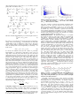
Figure 2: Delay ratios between (c1 , c0 ) and (c2 , c0 ), respectively.
c0 = (SS, 0.9V, -25◦ C, Cmax), c1 = (SS, 0.75V, -25◦ C, Cmax)
and c2 = (FF, 1.1V, 125◦ C, Cmin).
+ ∆cj0 )
(Dcjk0 + ∆cjk0 ) −
s j0 ∈Pi0
0
Dcjk0 −
+ ∆cjk ))
k
s j ∈Pi
∑ (Dcj
∑
∑ (Dcj
s j ∈Pi
Dcjk ) − (
k
+ ∆cjk ))
∑
s j0 ∈Pi0
Dcj00 −
s j ∈Pi
(8)
We also bound the maximum latency for each clock path as follows.
∑ (Dcj
s j ∈Pi
k
+ ∆cjk ) ≤ Dmax
(9)
For each arc, we specify the upper and lower bounds on the latency
k
change. The lower bound Dcmin
j is determined by the delay with
optimal buffer insertion, without any routing detour. The upper
bound of delay change is defined as β times of the original arc
delay, in which β can be selected empirically (we assume β = 1.2
in this work).
ck
ck
ck
k
Dcmin
j ≤ Dj +∆j ≤ β·Dj
(10)
To increase the likelihood that the LP solution is practically
implementable, we characterize lookup tables at each corner for
stage delays of inverter pairs3 with various gate sizes and routed
wirelengths between consecutive inverters. We define the stage
delay between inverter pairs as the sum of gate delays of the two
inverters in a pair and the delays of their fanout nets (Figure 3).
Based on the characterized lookup tables, we observe that for a
given stage delay per unit distance at c0 (i.e., the ratio between stage
delay and routed wirelength for an inverter pair), the stage delay
ratios between pairs of corners are limited by the buffer insertion
solutions in lookup tables. Figure 2 shows the stage delay ratios
between pairs of corners (c0 , c1 ) and (c0 , c2 ), respectively. In the
plot, each circle represents an inverter pair with a particular gate
size, routed wirelength between consecutive inverters, input slew
and load capacitance. We use polynomial fit to determine upper
ck ,ck0
ck ,ck0
(Wmax
) and lower (Wmin
) bounds of delay ratios for each pair
of corners, which are shown as the red curves. Any delay ratio
larger (smaller) than the upper (lower) bound is not achievable with
available buffer insertion solutions in lookup tables. Furthermore,
we assume that the delay per unit distance of an arc does not vary
significantly in our optimization due to Constraints (7)-(10). Thus,
we use delay per unit distance of an arc in the original clock tree
ck ,ck0
to estimate upper and lower bounds of delay ratios (Wmin,max
), and
apply these bounds in Constraint (11) to avoid LP solutions that are
not practically implementable by ECOs.
c ,c
0
k k
Wmin
≤
Dcjk + ∆cjk
c
0
c
D jk + ∆ jk
c ,c
0
k k
≤ Wmax
0
(11)
Complexity Analysis. The LP formulation (Equations (4)-(11))
has O(M · K) variables to indicate delay change on each arc at
each corner (∆cjk ); there are also O(N 2 ) (i.e., the number of
3 In this work, we assume that the buffers used to construct the clock
tree are comprised of inverter pairs. But, our methodologies apply
to clock trees with both inverting and non-inverting buffers.
sink pairs) variables to indicate the maximum normalized skew
variation across all corner pairs between each sink pair (Vi,i0 ).
There are C(K, 2) constraints to force Vi,i0 to be no less than
the maximum normalized skew variation between each sink pair
(Constraint (6)); (4 · K) constraints to prevent local skew and
skew variation degradations (Constraints (7)-(8)); N constraints to
specify the maximum latency (Constraint (9)); (2·M) constraints to
bound arc delay changes (Constraint (10)); and C(K, 2) constraints
to enhance ECO feasibility (Constraint (11)).
ECO Implementation. We apply ECO changes to accomplish
the desired arc delays at each corner, which are determined by
LP solution. Given that the buffer insertion problem is NPcomplete [19], although we apply several techniques to enhance
ECO feasibility, the LP formulation still cannot guarantee an
optimal solution that is practically implementable. Thus, our
target is to minimize the discrepancy between the desired delays
in the LP solution and those that actually result from ECOs. In
our ECO implementation, we first remove all original inverter
pairs on the arc. We then determine the solution (i.e., gate
size and routed wirelengths between consecutive inverters) of
inverter pair insertion based on the characterized lookup tables
with stage delays. Note that in this work, we always use one
gate size, and uniformly place inverter pairs, for each individual
arc. We place inverter pairs in a “U” shape when routing
detour is required. The lookup table contains stage delays with
five inverter sizes and routed wirelengths between consecutive
inverters varying from 10µm to 200µm with a step size of
5µm across different corners. Since these lookup tables are
technology-dependent, we only perform the characterization once
per technology. More specifically, we have two lookup tables: (i)
LUTdetail is characterized with different input slew and fanout load
capacitance, and is applied for the first and last inverter pairs of
a given arc, and (ii) LUTuni f orm is characterized based on average
stage delay of inverter pairs in an arc, and is applied for the inverter
pairs in the middle of an arc (Figure 3).
Figure 3: LUTdetail is characterized with various input slews
and fanout loads capacitance; LUTuni f orm contains average
stage delay with particular gate size and routed wirelengths
between consecutive inverters.
Algorithm 1 describes the flow to select solutions for inverter
pair insertions. For each combination of gate size and routed
wirelength between consecutive inverters, we estimate a range of
desired number of inverter pairs (i.e., [max(uest − 2, 0), uest + 2])
based on the average stage delay in LUTuni f orm at corner c0
k
(Lines 5-6). DcLP
is the required arc delay at corner ck in the
LP solution. We then assess error for each potential solution
(i.e., a combination of gate size, routed wirelength between
consecutive inverters and number of inverter pairs) and select the
solution with minimum error (Lines 7-16). We use p and q to
respectively index the gate size and the routed wirelength between
consecutive inverters. Dcestk is the estimated delay using LUTs.
Last, we implement ECO changes based on the selected solution
(Lines 19, 21).
Algorithm 1 LP-guided ECO flow.
1: for all s j to be optimized do
2: Remove current inverter pairs on s j
3: errmin ← +∞; sol ← 0/
4: for p := 1 to Nsize , q := 1 to NW L do
ck
ck
5:
uest ← round(DLP
/d(LUTuni f orm ) p,q
)
6:
for u := max(uest − 2, 0) to uest + 2 do
7:
err ← 0
8:
for k := 0 to K do c
ck
9:
err ← err + |Destk − DLP
|
10:
end for
11:
for all corner pair (ck , ck0 ) do
c 0
ck 0
c
ck
12:
err ← err + |(Destk − Destk ) − (DLP
− DLP
)|
13:
end for
14:
if err < errmin then
15:
errmin ← err; sol ← (p, q, u)
16:
end if
17:
end for
18: end for
19: Perform ECO inverter pair insertion based on sol
20: end for
21: Legalize all inserted inverters and perform ECO routing
4.2
Local Optimization
We apply local iterative optimization to further minimize the sum
of skew variations across corners. More specifically, we consider
three types of local moves, which are illustrated in Figure 4(b)-(d)
– (I) buffer sizing and/or buffer displacement, (II) displacement of
a buffer and gate sizing on one of its child buffers, and (III) tree
surgery (i.e., reassignment of a (child) node to a different (parent)
driver). However, performance of such iterative optimization is
usually limited by its large turnaround time. For instance, each
local move requires placement legalization, ECO routing, parasitic
extraction, and timing analysis in the golden timer.4 Given such
large turnaround time, it is practically impossible to explore all
possible local moves for a given design. Therefore, a fast and
accurate model to predict the impact of local moves is necessary.
Previous work [8] has demonstrated that machine learning-based
models are quite accurate for delay and slew estimation. In our
work, we apply a two-stage machine learning-based model for
prediction of arc delay changes with local moves. The overarching
goal is to be able to accurately predict delta-latency, i.e., the change
in post-ECO routing source-sink delays that results from a given
buffer’s resizing and/or placement perturbation.
Figure 4: Local optimization moves used in our flow. (a)
Initial subtree; (b) sizing and/or displacement, (c) displacement
and sizing of child node, and (d) tree surgery, i.e., driver
reassignment.
Machine Learning-Based Model. To predict the impact of a local
move, we first estimate new routing pattern (if the move contains
displacement or tree surgery) by constructing two types of trees –
FLUTE [3] tree and single-trunk Steiner tree. We approximate wire
delays correspondingly using Elmore delay and D2M [1] models.
4 In
our experiments, the runtime for each local move on a testcase
with 1.79M instances and 270K flip-flops, using one thread per
analysis corner on a 2.5GHz Intel Xeon server, is around 70
minutes (i.e., 30 minutes for ECO and parasitic extraction, and 40
minutes for timing analysis).
We then update the delay and output slew of the driver based
on the estimated wire capacitance and update pin capacitance (if
the move sizes the child node) by performing interpolation in the
Liberty table. Last, we perform slew propagation using PERI [14]
and update gate delays one and two stages downstream based on
Liberty tables.5 However, as observed in [8], the interpolated delay
values do not always match those from the golden timer’s analysis.
Further, the estimated routing pattern as well as wire delay can have
discrepancy with respect to the commercial router’s actual ECO
solution.
We therefore construct machine learning-based models to
minimize such discrepancy. We use Artificial Neural Networks
(ANN) [9], Support Vector Machines (SVM) with a Radial
Basis Function (RBF) kernel [9], and Hybrid Surrogate Modeling
(HSM) [13].6 In addition to the estimated delays based on {FLUTE
tree, single-trunk Steiner tree} × {Elmore delay, D2M}, the input
parameters to the machine learning-based model also include the
number of fanout cells, as well as the area and aspect ratio of
the bounding box which contains driving pin and fanout cells. To
generate training data, we construct artificial testcases (i.e., clock
trees) that resemble real designs with fanout ranging from 1-5 (2040 for last-stage buffers) and bounding box area and aspect ratio
of the driven pins ranging from 1000µm2 to 8000µm2 and from 0.5
to 1, respectively. We then place fanout cells or sinks randomly
within the bounding box. We generate 150 artificial testcases and
perform 450 moves on average to each testcase (the runtime for
one testcase is ∼1 hour). Note that we only construct one model
for each corner, and that this model is applied to all designs.
Figure 5: Examples of (a) predicted vs. actual latencies, and
(b) percentage error histograms from our model for c3 corner
in Table 3.
We create one delta-latency model for each corner used in our
experiments. Figure 5(a) shows the predicted vs. actual latencies
that we compute from the predicted delta latencies by our model
at corner c3 in Table 3. Figure 5(b) shows the corresponding
histogram of percentage errors. Across all the corners, our
modeling error is 2.8% on average. The absolute of maximum
and minimum errors are 21.98% and 16.21% respectively. The
modeling for each corner using the artificial testcases is a one-time
effort. On a 2.5GHz Intel Xeon server, the time to train a model
for each corner is around 5 hours with four threads. Models for
each corner can be trained in parallel, e.g., on a server with 24
threads, we can train six models in 5 hours. Our models generalize
to different testcases because (i) our training dataset generated
from the artificial testcases span ranges of parameters that are
typically seen in clock trees in SOC application processors and
memory controllers, and (ii) we prevent overfitting by performing
cross-validation. Our experimental results indicate that our models
are generalizable and accurate when applied to “unseen” testcases
during the model training phase. Figure 6 shows the accuracy
comparison between our learning-based model and analytical
models. We observe that with fewer attempts, our learning-based
model is able to identify the best move for more buffers.
Iterative Optimization Flow. Based on our model, we perform
iterative local optimization flow illustrated in Algorithm 2. We first
enumerate all candidate local moves and generate the input data
to our model (Line 1). The moves we consider in this work are
5 Our
analyses show that the delay and slew change of buffers
beyond two stages is <1ps, so we do not update timings of buffers
beyond two stages downstream.
6 Further details of the applied machine-learning techniques that we
use may be found in [9] and [13].
(ILMs) to resemble four cores of an application processor. These
are floorplanned in a rectangular block such that the utilization of
standard cells is ∼60% before placement.7 Figure 7(a) shows the
floorplan of CLS1v1. We implement the CLS1 class testcases at
corners c0 , c1 and c3 as shown in Table 4. Corners c0 and c1 are
setup-critical, and c3 is hold-critical. Table 4 summarizes various
post-synthesis metrics of these testcases.
Figure 6: Accuracy comparison between our learning-based
model and analytical models. An attempt is an ECO. There are
114 buffers, and each buffer has 45 candidate moves. In one
attempt, the learning-based model (resp. analytical models)
can identify best moves for 40% (resp. up to 20%) of the
buffers.
shown in Table 2. We predict the delta-latency resulting from each
move based on our model (Line 2). We then estimate the skew
variation reductions based on the predicted latency changes. Our
experimental results show that we are able to evaluate the impacts
of more than 160K moves at three corners in 17 min on a 2.5GHz
Intel Xeon server with 15 threads. We sort the candidate moves in
decreasing order of their predicted skew variation reductions, and
pick the top R (i.e., R = 5 in this work) moves to implement in R
individual threads (Line 3). Last, we perform timing analysis using
the golden timer to assess the actual skew variation changes (Line
4). If there is skew variation reduction, we update the database with
the minimum skew variation solution. Otherwise, we implement
the next R moves (Lines 5-9). The iteration terminates when there
is no move showing skew variation reduction according to our
predictor.
Algorithm 2 Iterative optimization flow.
1:
2:
3:
4:
5:
6:
7:
8:
9:
Enumerate all candidate moves and generate input data to model
Predict delta-latency and skew variation reductions
Implement R moves with maximum predicted skew variation reductions using R
threads
Assess actual skew variation reductions with the golden timer
if there is skew variation reduction then
Update database with the minimum skew variation solution
else
Implement the next R moves and go to Line 4
end if
Table 2: Candidate moves in our optimization.
Type
Candidate moves
I
displace {N, S, E, W, NE, NW, SE, SW} by 10µm × one-step up/down sizing
displace {N, S, E, W, NE, NW, SE, SW} by 10µm × one-step up/down sizing
II
on one child node
reassign to a new driver (i) at the same level as current driver, and (ii) within
III
bounding box of 50µm × 50µm
5.
EXPERIMENTAL RESULTS
Our experiments are implemented in foundry 28nm LP
technology. We construct the original clock tree and perform
ECO optimizations using Synopsys IC Compiler [25]. We use
Synopsys PrimeTime [26] and Synopsys PT-PX for timing and
power analyses, respectively. We construct the machine learningbased model using MATLAB [24]. The optimization flow is
implemented using C++ and Tcl scripts.
5.1
Testcase Description
We have developed two classes of testcase generators to validate
our proposed optimization framework. Class CLS1 corresponds
to clock networks typically observed in high-speed application
processors and graphics processors. Class CLS2 corresponds to
clock networks in memory controllers, which are typically used
in SoCs to interface SoC components with DRAM/eDRAM. We
implement our testcases at 28nm LP technology. The corners
used in our experiments are shown in Table 3. We use the
testcase generation methodology described in [5], and the toplevel structures of the testcases T1 and T2 in [5]. We modify
the floorplan and clock tree synthesis flow to develop two variants
of CLS1, CLS1v1 and CLS1v2. Each of CLS1v1 and CLS1v2
contains four identical 650µm × 650µm interface logic modules
Figure 7: Floorplans of (a) CLS1v1, and (b) CLS2v1. In yellow
are routed clock nets.
Table 3: Description of corners.
Corner Process Voltage Temperature Back-end-of-line
c0
ss
0.90V
-25◦ C
Cmax
c1
ss
0.75V
-25◦ C
Cmax
c2
ff
1.10V
125◦ C
Cmin
c3
ff
1.32V
125◦ C
Cmin
Table 4: Summary of testcases.
Testcase
CLS1v1
CLS1v2
CLS2v1
#Cells
0.4M
0.4M
1.79M
#Flip-flops
36K
35K
270K
Area
3.3mm2
3.4mm2
4.5mm2
Util
62%
60%
58%
Corners
c0 , c1 , c3
c0 , c1 , c3
c0 , c1 , c2
We also study a testcase CLS2v1 of class memory controller,
which is new as compared to [5]. Table 4 summarizes the
post-synthesis metrics of this testcase, and Figure 7(b) shows
its floorplan. We use the methodology described in [5] to
generate random logic and connect this logic to FFs; this includes
datapaths across different clock groups. The memory controller
is floorplanned in an L-shaped block with the controller at the
center and the interface logic in each of the top and bottom arms
of the L-shape. The interface logic has data and control signals
across memory, processor and other blocks. The control signals are
generated within the controller, and the FFs in the interface logic
and controller are separated by large distances (e.g., ∼1mm). The
large distance between sequentially adjacent sinks leads to large
clock skew, which the commercial tool tries to balance by inserting
buffers. However, these clock buffers lead to skew variations across
corners. We implement the CLS2v1 testcase at corners c0 , c1 and
c2 as shown in Table 4, where c0 and c1 are setup-critical and c2 is
hold-critical.
For implementations of all our testcases, we follow a production
methodology [23]. We set the skew target as 0ps in the CTS tools,
as our studies (with skew targets ranging from 0ps to 250ps, in
steps of 50ps) indicate that a target skew of 0ps steers the tool
to deliver the smallest skew at each corner. We perform clock
tree optimizations with both multi-corner multi-mode (MCMM)
scenario as well as multi-corner single-mode (MCSM) scenario at
each mode. We then select the optimized clock tree solution with
minimum skew variation as the input to our optimization.
5.2
Results
Table 5 shows the experimental results,8 where variation, skew,
#cells, power and area are respectively the sum of normalized
skew variations over union of top 10K critical sink pairs (in terms
of setup and hold timing slacks) at each corner,9 local skew at
each corner, total number of clock cells, clock tree power and
total area of clock cells. In the experiments, we apply three
7 We understand from our industry collaborators that best-practices
flows for high-speed and memory controller blocks start with 50%–
60% utilization before placement [23].
8 Our optimization does not create any maximum transition or
maximum capacitance violations.
9 The number of optimized sink pairs for CLS1v1, CLS1v2 and
CLS2v2 are respectively 15012, 14671 and 15142.
optimization flows to each of the testcases: (i) global is the
global optimization flow, (ii) local is the local iterative optimization
flow, and (iii) global-local performs global and local optimizations
in sequence. The global (local) optimization alone achieves up
to 16% (5%) reduction on the sum of skew variations. Since
local moves affect only a subset of sink pairs, they have smaller
impact than that of the global optimization. By combining the
two optimizations, we reduce the sum of skew variations by 22%
with negligible area and power overhead. The results also show
no degradation of local skews. Further, we observe that the local
iterative optimization reduces skew variations more when applied
after the global optimization, as compared to a standalone local
skew optimization (e.g., for CLS1v1, local optimization achieves
13ns more reduction with a prior global optimization, as compared
to the standalone local optimization).
Table 5: Experimental results.
Variation [norm]
(ns)
orig
512 [1.00]
global
431 [0.84]
CLS1v1
local
493 [0.96]
global-local
399 [0.78]
orig
585 [1.00]
global
518 [0.89]
CLS1v2
local
557 [0.95]
global-local
510 [0.87]
orig
972 [1.00]
global
888 [0.91]
CLS2v1
local
926 [0.95]
global-local
841 [0.87]
Testcase
Flow
Skew (ps)
Power
#Cells
c0 c1 c2,3
(mW )
214 530 226 2515 0.355
179 395 188 2553 0.356
214 529 223 2515 0.355
175 387 188 2553 0.356
272 594 259 2762 0.369
269 575 235 2762 0.369
258 545 259 2762 0.369
265 564 235 2762 0.369
179 192 282 5568 0.865
175 192 232 5574 0.866
180 190 282 5568 0.865
176 192 232 5574 0.866
Area
(µm2 )
3615
3705
3621
3706
3968
3975
3970
3975
8556
8577
8556
8557
Figure 8 shows the skew variation reduction during the local
iterative optimization. We observe that tree surgeries (type-I
moves) are more effective than sizing and displacement moves
(type-II and type-III moves), and are applied by our model in the
early iterations. For CLS1v1, we also show the results with 10
random moves (dots in black), where the gap between random
move and our optimization is 15ns. This validates the benefits
of our delta-latency model. The runtimes per iteration (with 15
threads) are 60 min, 80 min and 200 min for testcases CLS1v1,
CLS1v2 and CLS2v1, respectively.
Figure 8: Sum of skew variations reduces during the local
iterative optimization. In blue are type-I moves, in red are typeII moves, and in green are type-III moves.
Figure 9 shows the distributions of skew ratios between corner
pairs (c1 , c0 ) and (c3 , c0 ), over sink pairs, of the initial clock tree
and the optimized clock tree. We observe that our optimization
significantly reduces the variation and range of skew ratios between
corner pairs.
6.
CONCLUSION
In this work, we propose the first framework to minimize the
sum of skew variations over all sequentially adjacent sink pairs,
using both global and local optimizations. Our experimental results
show that the proposed flow achieves up to 22% reduction of the
sum of skew variations for testcases implemented in foundry 28nm
technology, as compared to a leading commercial tool. In the
global optimization, our LP formulation comprehends the ECO
feasibility based on characterized lookup tables of stage delays. In
the local optimization, we demonstrate that machine learning-based
predictors of latency changes can provide accurate estimation of
local move impacts.
Our future works include: (i) study of the resultant power and
area benefits of reduced skew variation; (ii) development of models
to predict a buffer location for minimum skew over a continuous
range of possible buffer locations; (iii) explorations, motivated by
our current results, of new library cells whose delay and slew are
Figure 9: Distribution of skew ratios between (c1 , c0 ) and (c3 ,
c0 ) of (i) original clock tree, and (ii) optimized clock tree for
CLS1v1.
less sensitive to corner variation so as to enable fine-grained ECOs
based on our LP solutions; and (iv) investigation of whether a worse
initial start point (clock network with large skew variations) can
enable us to achieve smaller skew variation across corners using
our optimization flow.
7.
REFERENCES
[1] C. J. Alpert, A. Devgan and C. Kashyap, “A Two Moment RC Delay Metric
for Performance Optimization”, Proc. ISPD, 2000, pp. 73-78.
[2] J. Bhasker and R. Chadha, Static Timing Analysis for Nanometer Designs: A
Practical Approach, Springer, 2009.
[3] C. Chu, “FLUTE: Fast Lookup Table Based Wirelength Estimation
Technique”, Proc. ICCAD, 2004, pp. 696-701.
[4] A. Cao, S.-M. Chang and D.-C. Yuan, “Local Clock Skew Optimization”, US
Patent No. 8,635,579, 2014.
[5] T.-B. Chan, K. Han, A. B. Kahng, J.-G. Lee and S. Nath, “OCV-Aware
Top-Level Clock Tree Optimization”, Proc. GLSVLSI, 2014, pp. 33-38.
[6] M. Cho, S. Ahmed and D. Z. Pan, “TACO: Temperature Aware Clock-tree
Optimization”, Proc. ICCAD, 2005, pp. 582-587.
[7] H.-M. Chou, H. Yu and S.-C. Chang, “Useful-Skew Clock Optimization for
Multi-Power Mode Designs”, Proc. ICCAD, 2011, pp. 647-650.
[8] S. S. Han, A. B. Kahng, S. Nath and A. Vydyanathan, “A Deep Learning
Methodology to Proliferate Golden Signoff Timing”, Proc. DATE, 2014, pp.
1-6.
[9] T. Hastie, R. Tibshirani and J. Friedman, The Elements of Statistical Learning:
Data Mining, Inference, and Prediction, Springer, 2009.
[10] C.-L. Lung, H.-C. Hsiao, Z.-Y. Zeng and S.-Y. Chang, “LP-Based Multi-Mode
Multi-Corner Clock Skew Optimization”, Proc. VLSI-DAT, 2010, pp. 335-338.
[11] C.-L. Lung, Z.-Y. Zeng, C.-H. Chou and S.-Y. Chang, “Clock Skew
Optimization Considering Complicated Power Modes”, Proc. DATE, 2010, pp.
1474-1479.
[12] A. B. Kahng, J. Lienig, I. L. Markov and J. Hu, VLSI Physical Design: From
Graph Partitioning to Timing Closure, Springer, 2011.
[13] A. B. Kahng, B. Lin and S. Nath, “Enhanced Metamodeling Techniques for
High-Dimensional IC Design Estimation Problems”, Proc. DATE, 2013, pp.
1861-1866.
[14] C. V. Kashyap, C. J. Alpert, F. Liu and A. Devgan, “PERI: A Technique for
Extending Delay and Slew Metrics to Ramp Inputs”, Proc. TAU, 2002, pp.
57-62.
[15] T. Mittal and C.-K. Koh, “Cross Link Insertion for Improving Tolerance to
Variations in Clock Network Synthesis”, Proc. ISPD, 2011, pp. 29-36.
[16] A. Rajaram, J. Hu and R. Mahapatra, “Reducing Clock Skew Variability via
Crosslinks”, Proc. DAC, 2004, pp. 18-23.
[17] A. Rajaram and D. Z. Pan, “Variation Tolerant Buffered Clock Network
Synthesis with Cross Links”, Proc. ISPD, 2006, pp. 157-164.
[18] P. J. Restle, T. G. McNamara, D. A. Webber, P. J. Camporese, K. F. Eng, K. A.
Jenkins, D. H. Allen, M. J. Rohn, M. P. Quaranta, D. W. Boerstler, C. J.
Alpert, C. A. Carter, R. N. Bailey, J. G. Petrovick, B. L. Krauter, and B. D.
McCredie, “A Clock Distribution Network for Microprocessors”, IEEE J.
Solid-State Circuits 36(5) (2001), pp. 792-799.
[19] W. Shi and Z. Li and C. Alpert, “Complexity Analysis and Speedup
Techniques for Optimal Buffer Insertion with Minimum Cost”, Proc.
ASPDAC, 2004, pp. 609-614.
[20] H. Su and S. S. Sapatnekar, “Hybrid Structured Clock Network Construction”,
Proc. ICCAD, 2001, pp. 333-336.
[21] S. Sunder and K. Scholtman, “Multi-Mode Multi-Corner Clocktree
Synthesis”, US Patent No. US20090217225 A1, 2009.
[22] G. Venkataraman, N. Jayakumar, J. Hu, P. Li and S. Khatri, “Practical
Techniques to Reduce Skew and Its Variations in Buffered Clock Networks”,
Proc. ICCAD, 2005, pp. 592-596.
[23] Samsung Electronics Corporation (System LSI application processor principal
engineer), personal communication, July 2014.
[24] “MATLAB.” http://www.mathworks.com/products/matlab/
[25] “Synopsys IC Compiler User Guide.”
[26] “Synopsys PrimeTime User’s Manual.”