1
ISSN: 2277-9655
[Sakhare, 2(4): April, 2013]
Dual Tone Multi Frequency Technology
I. Dual tone multi frequency technology uses
mixture of two pure tones to represent a digit pressed
on the phone keypad..The DTMF keypad is a 4×4
matrix, with each row representing a low frequency,
and each column representing a high frequency. On
pressing a single key (such as 1), a sinusoidal tone is
sent for each of the two frequencies (697 and
1209Hz). The tones are sent to a DTMF decoder
which converts these tones into corresponding 4 bit
BCD number. In our project, the user selects alert
options by pressing a key on the keypad. Received
DTMF tone is then decoded and processed by the
microcontroller to identify the alert option selected.
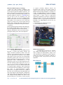
II. M-8870
M-8870 operating function include a band split filter
that separates the high and low tones of the received
pair, and a digital decoder that verifies both the
frequency and duration of the received tones before
passing the resulting 4-bit code to the output bus.
of registers providing enhanced features and
accelerated port access or the legacy group of
registers. We use GPIO pins to take the data from
DTMF decoder and then transmit it to computer via
UART1. The ARM7TDMI-S processor also employs
a unique architectural strategy known as THUMB,
which makes it ideally suited to high-volume
applications with memory restrictions, or applications
where code density is an issue. The key idea behind
THUMB is that of a super-reduced instruction set.
Essentially, the ARM7TDMI-S processor has two
instruction sets:
1. The standard 32-bit ARM instruction set.
2. 16-bit THUMB instruction set.
Microcontroller ARM LPC2148
In our project we have used ARM processor
LPC2148. A 128-bit wide memory interface and
unique accelerator architecture enable 32-bit code
execution at the maximum clock rate. For critical
code size applications, the alternative 16-bit Thumb
mode reduces code by more than 30 % with minimal
performance penalty. Due to their tiny size and low
power consumption, the LPC214x family is ideal for
applications where miniaturization is a key
requirement, such as access control and point-of-sale.
The CPU operating voltage ranges from 3.0 V to 3.6
V (3.3 V ± 10 %) with 5 V tolerant I/O pads. The
ARM architecture is based on Reduced Instruction
Set Computer (RISC) principles, and the instruction
set and related decode mechanism are much simpler
than those of Micro-programmed Complex
Instruction Set Computers. We use two UARTs of
LPC2148, one for interfacing with GSM module and
other with computer. Microcontroller communicates
with GSM module through RXD0 and TXD0 and
with computer through RXD1 and TXD1. Every
physical GPIO port is accessible via either the group
MAX 232 Serial Interface
A standard RS-232 interface for computer
uses voltage levels ranging from -12V to +12V. In
order to adjust the microcontroller voltage levels
(TTL standards) for compatibility with the computer,
voltage level converters are necessary. Max-232, is
an integrated circuit, that provides this necessary
adjustment.
http: // www.ijesrt.com
Block Diagram
(C) International Journal of Engineering Sciences & Research Technology[863-866]