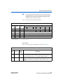
1
Nios II Processor Reference Handbook
101 Innovation Drive
San Jose, CA 95134
(408) 544-7000
http://www.altera.com
NII5V1-1.2
Copyright © 2003 Altera Corporation. All rights reserved. Altera, The Programmable Solutions Company, the stylized Altera logo, specific device designations, and all other words and logos that are identified as trademarks and/or service marks are, unless noted otherwise, the trademarks and
service marks of Altera Corporation in the U.S. and other countries. All other product or service names are the property of their respective holders. Altera products are protected under numerous U.S. and foreign patents and pending applications, maskwork rights, and copyrights. Altera warrants
performance of its semiconductor products to current specifications in accordance with Altera's standard warranty, but reserves the right to make
changes to any products and services at any time without notice. Altera assumes no responsibility or liability arising out of the application or use of any information, product, or service described herein except as expressly agreed to in writing by Altera
Corporation. Altera customers are advised to obtain the latest version of device specifications before relying on any published information and before placing orders for products or services.
Printed on recycled paper
ii
Altera Corporation
Contents
Chapter Revision Dates ........................................................................... xi
About This Handbook ............................................................................ xiii
Introduction ............................................................................................................................................ xiii
Assumptions about the Reader .................................................................................................. 1–xiii
How to Find Further Information ....................................................................................................... xiii
How to Contact Altera .......................................................................................................................... xiv
Typographical Conventions ................................................................................................................. xiv
Section I. Nios II Processor
Revision History ....................................................................................................................... Section I–2
Chapter 1. Introduction
Introduction ............................................................................................................................................ 1–1
Nios II Processor System Basics ..................................................................................................... 1–1
Getting Started with the Nios II Processor ................................................................................... 1–2
Customizing Nios II Processor Designs ........................................................................................ 1–3
Configurable Soft-Core Processor Concepts ...................................................................................... 1–3
Configurable Soft-Core Processor .................................................................................................. 1–4
Flexible Peripheral Set & Address Map ........................................................................................ 1–4
Custom Instructions ......................................................................................................................... 1–5
Automated System Generation ...................................................................................................... 1–5
Chapter 2. Processor Architecture
Introduction ............................................................................................................................................ 2–1
Processor Implementation .................................................................................................................... 2–2
Register File ............................................................................................................................................ 2–3
Arithmetic Logic Unit ........................................................................................................................... 2–3
Unimplemented Instructions .......................................................................................................... 2–4
Custom Instructions ......................................................................................................................... 2–4
Exception & Interrupt Controller ........................................................................................................ 2–4
Exception Controller ........................................................................................................................ 2–4
Integral Interrupt Controller ........................................................................................................... 2–4
Memory & I/O Organization .............................................................................................................. 2–5
Instruction & Data Buses ................................................................................................................. 2–6
Cache Memory .................................................................................................................................. 2–8
Address Map ..................................................................................................................................... 2–9
JTAG Debug Module .......................................................................................................................... 2–10
Altera Corporation
iii
Contents
JTAG Target Connection ...............................................................................................................
Download & Execute Software ....................................................................................................
Software Breakpoints .....................................................................................................................
Hardware Breakpoints ..................................................................................................................
Hardware Triggers .........................................................................................................................
Trace Capture ..................................................................................................................................
2–11
2–11
2–11
2–11
2–11
2–13
Chapter 3. Programming Model
Introduction ............................................................................................................................................ 3–1
General-Purpose Registers ................................................................................................................... 3–1
Control Registers ................................................................................................................................... 3–2
Operating Modes ................................................................................................................................... 3–4
Supervisor Mode .............................................................................................................................. 3–5
User Mode ......................................................................................................................................... 3–5
Debug Mode ...................................................................................................................................... 3–6
Changing Modes .............................................................................................................................. 3–6
Exception Processing ............................................................................................................................. 3–8
Exception Types ................................................................................................................................ 3–8
Determining the Cause of Exceptions ......................................................................................... 3–11
Nested Exceptions .......................................................................................................................... 3–13
Returning from an Exception ...................................................................................................... 3–13
Break Processing .................................................................................................................................. 3–13
Processing a Break .......................................................................................................................... 3–14
Returning from a Break ................................................................................................................. 3–14
Register Usage ................................................................................................................................ 3–14
Memory & Peripheral Access ............................................................................................................ 3–15
Addressing Modes ......................................................................................................................... 3–15
Cache Memory ................................................................................................................................ 3–15
Processor Reset State ........................................................................................................................... 3–16
Instruction Set Categories ................................................................................................................... 3–17
Data Transfer Instructions ............................................................................................................ 3–17
Arithmetic & Logical Instructions ............................................................................................... 3–18
Move Instructions ........................................................................................................................... 3–19
Comparison Instructions ............................................................................................................... 3–19
Shift & Rotate Instructions ............................................................................................................ 3–20
Program Control Instructions ....................................................................................................... 3–21
Other Control Instructions ............................................................................................................ 3–22
Custom Instructions ....................................................................................................................... 3–22
No-Operation Instruction ............................................................................................................. 3–22
Potential Unimplemented Instructions ....................................................................................... 3–23
Chapter 4. Implementing the Nios II Processor in SOPC Builder
Introduction ............................................................................................................................................ 4–1
Nios II Core Tab ..................................................................................................................................... 4–2
Core Setting ....................................................................................................................................... 4–2
Cache Settings ................................................................................................................................... 4–3
Multiply & Divide Settings ............................................................................................................. 4–3
iv
Nios II Processor Reference Handbook
Altera Corporation
Contents
JTAG Debug Module Tab .....................................................................................................................
Debug Level Settings .......................................................................................................................
On-Chip Trace Buffer Settings .......................................................................................................
Custom Instructions Tab ......................................................................................................................
4–4
4–5
4–6
4–7
Section II. Peripheral Support
Revision History ..................................................................................................................... Section II–2
Chapter 5. SDRAM Controller with Avalon Interface
Core Overview ....................................................................................................................................... 5–1
Functional Description .......................................................................................................................... 5–1
Avalon Interface ............................................................................................................................... 5–2
Off-Chip SDRAM Interface ............................................................................................................. 5–3
Performance Considerations .......................................................................................................... 5–4
Device & Tools Support ........................................................................................................................ 5–5
Instantiating the Core in SOPC Builder ............................................................................................. 5–6
Memory Profile Tab ......................................................................................................................... 5–7
Timing Tab ........................................................................................................................................ 5–8
Hardware Simulation Considerations ................................................................................................ 5–9
Example Configurations ..................................................................................................................... 5–11
Software Programming Model .......................................................................................................... 5–13
Chapter 6. DMA Controller with Avalon Interface
Core Overview ....................................................................................................................................... 6–1
Functional Description .......................................................................................................................... 6–1
Setting Up DMA Transactions ....................................................................................................... 6–2
The Master Read & Write Ports ...................................................................................................... 6–3
Address Incrementing ..................................................................................................................... 6–3
Instantiating the Core in SOPC Builder ............................................................................................. 6–4
DMA Parameters (Basic) ................................................................................................................. 6–4
Advanced Options ........................................................................................................................... 6–5
Software Programming Model ............................................................................................................ 6–5
HAL System Library Support ......................................................................................................... 6–5
Software Files .................................................................................................................................... 6–7
Register Map ..................................................................................................................................... 6–8
Interrupt Behavior .......................................................................................................................... 6–11
Chapter 7. PIO Core With Avalon Interface
Core Overview .......................................................................................................................................
Functional Description ..........................................................................................................................
Data Input & Output .......................................................................................................................
Edge Capture ....................................................................................................................................
IRQ Generation .................................................................................................................................
Example Configurations .......................................................................................................................
Avalon Interface ...............................................................................................................................
Altera Corporation
7–1
7–1
7–2
7–3
7–3
7–4
7–4
v
Nios II Processor Reference Handbook
Contents
Instantiating the PIO Core in SOPC Builder ...................................................................................... 7–4
Basic Settings ..................................................................................................................................... 7–5
Input Options .................................................................................................................................... 7–5
Device & Tools Support ........................................................................................................................ 7–6
Software Programming Model ............................................................................................................ 7–6
Software Files .................................................................................................................................... 7–6
Legacy SDK Routines ...................................................................................................................... 7–7
Register Map ..................................................................................................................................... 7–7
Interrupt Behavior ............................................................................................................................ 7–9
Software Files .................................................................................................................................... 7–9
Chapter 8. Timer Core with Avalon Interface
Core Overview ....................................................................................................................................... 8–1
Functional Description .......................................................................................................................... 8–1
Avalon Slave Interface ..................................................................................................................... 8–2
Device & Tools Support ........................................................................................................................ 8–3
Instantiating the Core in SOPC Builder ............................................................................................. 8–3
Timeout Period ................................................................................................................................. 8–3
Hardware Options ........................................................................................................................... 8–3
Configuring the Timer as a Watchdog Timer .............................................................................. 8–4
Software Programming Model ............................................................................................................ 8–5
HAL System Library Support ......................................................................................................... 8–5
Software Files .................................................................................................................................... 8–6
Register Map ..................................................................................................................................... 8–6
Interrupt Behavior ............................................................................................................................ 8–9
Chapter 9. JTAG UART Core with Avalon Interface
Core Overview ....................................................................................................................................... 9–1
Functional Description .......................................................................................................................... 9–1
Avalon Slave Interface & Registers ................................................................................................ 9–2
Read & Write FIFOs ......................................................................................................................... 9–2
JTAG Interface .................................................................................................................................. 9–3
Host-Target Connection .................................................................................................................. 9–3
Device Support & Tools ........................................................................................................................ 9–4
Instantiating the Core in SOPC Builder ............................................................................................. 9–4
Configuration Tab ............................................................................................................................ 9–4
Simulation Settings .......................................................................................................................... 9–6
Hardware Simulation Considerations ................................................................................................ 9–7
Software Programming Model ............................................................................................................ 9–7
HAL System Library Support ......................................................................................................... 9–7
Software Files .................................................................................................................................. 9–11
Accessing the JTAG UART Core via a Host PC ......................................................................... 9–11
Register Map ................................................................................................................................... 9–11
Interrupt Behavior .......................................................................................................................... 9–13
Chapter 10. UART Core with Avalon Interface
Core Overview ..................................................................................................................................... 10–1
vi
Nios II Processor Reference Handbook
Altera Corporation
Contents
Functional Description ........................................................................................................................ 10–2
Avalon Slave Interface & Registers .............................................................................................. 10–2
RS-232 Interface .............................................................................................................................. 10–3
Transmitter Logic ........................................................................................................................... 10–3
Receiver Logic ................................................................................................................................. 10–4
Baud Rate Generation .................................................................................................................... 10–4
Device Support & Tools ...................................................................................................................... 10–4
Instantiating the Core in SOPC Builder ........................................................................................... 10–4
Configuration Settings ................................................................................................................... 10–5
Simulation Settings ........................................................................................................................ 10–8
Hardware Simulation Considerations .............................................................................................. 10–9
Software Programming Model .......................................................................................................... 10–9
HAL System Library Support ....................................................................................................... 10–9
Software Files ................................................................................................................................ 10–13
Legacy SDK Routines .................................................................................................................. 10–13
Register Map ................................................................................................................................. 10–13
Interrupt Behavior ........................................................................................................................ 10–20
Chapter 11. SPI Core with Avalon Interface
Core Overview ..................................................................................................................................... 11–1
Functional Description ........................................................................................................................ 11–1
Example Configurations ................................................................................................................ 11–2
Transmitter Logic ........................................................................................................................... 11–3
Receiver Logic ................................................................................................................................. 11–4
Master & Slave Modes ................................................................................................................... 11–4
Avalon Interface ............................................................................................................................. 11–7
Instantiating the SPI Core in SOPC Builder ..................................................................................... 11–7
Master/Slave Settings .................................................................................................................... 11–7
Data Register Settings .................................................................................................................... 11–9
Timing Settings ............................................................................................................................... 11–9
Device & Tools Support .................................................................................................................... 11–10
Software Programming Model ........................................................................................................ 11–10
Hardware Access Routines ......................................................................................................... 11–10
Software Files ................................................................................................................................ 11–12
Legacy SDK Routines .................................................................................................................. 11–12
Register Map ................................................................................................................................. 11–12
Chapter 12. EPCS Device Controller Core with Avalon Interface
Core Overview .....................................................................................................................................
Functional Description ........................................................................................................................
Avalon Slave Interface & Registers ..............................................................................................
Device & Tools Support ......................................................................................................................
Instantiating the Core in SOPC Builder ...........................................................................................
Software Programming Model ..........................................................................................................
HAL System Library Support .......................................................................................................
Software Files ..................................................................................................................................
Altera Corporation
12–1
12–2
12–3
12–4
12–4
12–5
12–5
12–5
vii
Nios II Processor Reference Handbook
Contents
Chapter 13. Common Flash Interface Controller Core with Avalon Interface
Core Overview .....................................................................................................................................
Functional Description ........................................................................................................................
Device & Tools Support ......................................................................................................................
Instantiating the Core in SOPC Builder ...........................................................................................
Attributes Tab .................................................................................................................................
Timing Tab ......................................................................................................................................
Software Programming Model ..........................................................................................................
HAL System Library Support .......................................................................................................
Software Files ..................................................................................................................................
13–1
13–1
13–2
13–2
13–2
13–4
13–4
13–4
13–5
Chapter 14. System ID Core with Avalon Interface
Core Overview .....................................................................................................................................
Functional Description ........................................................................................................................
Device & Tools Support ......................................................................................................................
Instantiating the Core in SOPC Builder ...........................................................................................
Software Programming Model ..........................................................................................................
Software Files ..................................................................................................................................
14–1
14–1
14–2
14–2
14–2
14–4
Chapter 15. Character LCD (Optrex 16207) Controller with Avalon Interface
Core Overview ..................................................................................................................................... 15–1
Functional Description ........................................................................................................................ 15–1
Device & Tools Support ...................................................................................................................... 15–2
Instantiating the Core in SOPC Builder ........................................................................................... 15–2
Software Programming Model .......................................................................................................... 15–2
HAL System Library Support ....................................................................................................... 15–2
Displaying Characters on the LCD .............................................................................................. 15–3
Software Files .................................................................................................................................. 15–4
Register Map ................................................................................................................................... 15–4
Interrupt Behavior .......................................................................................................................... 15–4
Chapter 16. Mutex Core with Avalon Interface
Core Overview .................................................................................................................................... 16–1
Functional Description ........................................................................................................................ 16–1
Device and Tools Support .................................................................................................................. 16–2
Instantiating the Core in SOPC Builder ........................................................................................... 16–2
Software Programming Model .......................................................................................................... 16–3
Software Files .................................................................................................................................. 16–3
Hardware Mutex ............................................................................................................................ 16–3
Multiprocessor Synchronization .................................................................................................. 16–5
Interprocessor Mailbox .................................................................................................................. 16–8
Mutex API .......................................................................................................................................... 16–11
Section III. Appendixes
Revision History .................................................................................................................... Section III–1
viii
Nios II Processor Reference Handbook
Altera Corporation
Contents
Chapter 17. Nios II Core Implementation Details
Introduction .......................................................................................................................................... 17–1
Device Support ..................................................................................................................................... 17–3
Nios II/f Core ....................................................................................................................................... 17–3
Overview ......................................................................................................................................... 17–3
Register File ..................................................................................................................................... 17–4
Arithmetic Logic Unit .................................................................................................................... 17–4
Memory Access ............................................................................................................................... 17–6
Execution Pipeline .......................................................................................................................... 17–7
Instruction Performance ................................................................................................................ 17–9
Exception Handling ..................................................................................................................... 17–10
JTAG Debug Module ................................................................................................................... 17–11
Unsupported Features ................................................................................................................. 17–11
Nios II/s Core .................................................................................................................................... 17–11
Overview ....................................................................................................................................... 17–11
Register File ................................................................................................................................... 17–12
Arithmetic Logic Unit .................................................................................................................. 17–12
Memory Access ............................................................................................................................. 17–13
Execution Pipeline ........................................................................................................................ 17–14
Instruction Performance .............................................................................................................. 17–15
Exception Handling ..................................................................................................................... 17–16
JTAG Debug Module ................................................................................................................... 17–16
Unsupported Features ................................................................................................................. 17–17
Nios II/e Core .................................................................................................................................... 17–17
Overview ....................................................................................................................................... 17–17
Register File ................................................................................................................................... 17–17
Arithmetic Logic Unit .................................................................................................................. 17–18
Memory Access ............................................................................................................................. 17–18
Instruction Execution Stages ....................................................................................................... 17–18
Instruction Performance .............................................................................................................. 17–18
Exception Handling ..................................................................................................................... 17–19
JTAG Debug Module ................................................................................................................... 17–19
Unsupported Features ................................................................................................................. 17–19
Chapter 18. Nios II Processor Revision History
Introduction ..........................................................................................................................................
Nios II Versions ....................................................................................................................................
Architecture Revisions ........................................................................................................................
Core Revisions ......................................................................................................................................
Nios II/f Core .................................................................................................................................
Nios II/s Core .................................................................................................................................
Nios II/e Core .................................................................................................................................
JTAG Debug Module Revisions ........................................................................................................
18–1
18–1
18–2
18–2
18–2
18–3
18–3
18–4
Chapter 19. Application Binary Interface
Data Types ............................................................................................................................................ 19–1
Memory Alignment ............................................................................................................................. 19–1
Altera Corporation
ix
Nios II Processor Reference Handbook
Contents
Register Usage ...................................................................................................................................... 19–2
Endianess of Data ................................................................................................................................ 19–3
Stacks ................................................................................................................................................ 19–3
Frame Pointer Elimination ............................................................................................................ 19–4
Call Saved Registers ....................................................................................................................... 19–4
Further Examples of Stacks ........................................................................................................... 19–5
Function Prologs ............................................................................................................................. 19–6
Arguments & Return Values .............................................................................................................. 19–8
Arguments ....................................................................................................................................... 19–8
Return Values ................................................................................................................................. 19–8
Chapter 20. Instruction Set Reference
Introduction .......................................................................................................................................... 20–1
Word Formats ...................................................................................................................................... 20–1
I-Type ............................................................................................................................................... 20–1
R-Type .............................................................................................................................................. 20–1
J-Type ............................................................................................................................................... 20–2
Instruction Opcodes ............................................................................................................................ 20–2
Assembler Pseudo-instructions ......................................................................................................... 20–5
Assembler Macros ............................................................................................................................... 20–6
Instruction Set Reference .................................................................................................................... 20–7
Index
x
Nios II Processor Reference Handbook
Altera Corporation
Chapter Revision Dates
The chapters in this book, Nios II Processor Reference Handbook, were
revised on the following dates. Where chapters or groups of chapters are
available separately, part numbers are listed.
About This Handbook
Revised:
September 2004
Chapter 1. Introduction
Revised:
Part number:
September 2004
NII51001-1.1
Chapter 2. Processor Architecture
Revised:
December 2004
Part number: NII51002-1.2
Chapter 3. Programming Model
Revised:
December 2004
Part number: NII51003-1.2
Chapter 4. Implementing the Nios II Processor in SOPC Builder
Revised:
December 2004
Part number: NII51004-1.2
Chapter 5. SDRAM Controller with Avalon Interface
Revised:
September 2004
Part number: NII51005-1.1
Chapter 6. DMA Controller with Avalon Interface
Revised:
December 2004
Part number: NII51006-1.2
Chapter 7. PIO Core With Avalon Interface
Revised:
September 2004
Part number: NII51007-1.1
Chapter 8. Timer Core with Avalon Interface
Revised:
September 2004
Part number: NII51008-1.1
Altera Corporation
xi
Chapter Revision Dates
Chapter 9. JTAG UART Core with Avalon Interface
Revised:
December 2004
Part number: NII51009-1.2
Chapter 10. UART Core with Avalon Interface
Revised:
September 2004
Part number: NII51010-1.1
Chapter 11. SPI Core with Avalon Interface
Revised:
September 2004
Part number: NII51011-1.1
Chapter 12. EPCS Device Controller Core with Avalon Interface
Revised:
September 2004
Part number: NII51012-1.1
Chapter 13. Common Flash Interface Controller Core with Avalon Interface
Revised:
December 2004
Part number: NII51013-1.2
Chapter 14. System ID Core with Avalon Interface
Revised:
September 2004
Part number: NII51014-1.1
Chapter 15. Character LCD (Optrex 16207) Controller with Avalon Interface
Revised:
September 2004
Part number: NII51019-1.0
Chapter 16. Mutex Core with Avalon Interface
Revised:
December 2004
Part number: NII51020-1.0
Chapter 17. Nios II Core Implementation Details
Revised:
December 2004
Part number: NII51015-1.2
Chapter 18. Nios II Processor Revision History
Revised:
December 2004
Part number: NII51018-1.1
Chapter 19. Application Binary Interface
Revised:
May 2004
Part number: NII51016-1.0
xii
Nios II Processor Reference Handbook
Altera Corporation
Chapter Revision Dates
Chapter 20. Instruction Set Reference
Revised:
December 2004
Part number: NII51017-1.2
Index
Revised:
Altera Corporation
December 2004
xiii
Nios II Processor Reference Handbook
Chapter Revision Dates
xiv
Nios II Processor Reference Handbook
Altera Corporation
About This Handbook
Introduction
The handbook you are holding (the Nios II Processor Reference Handbook) is
the primary reference for the Nios® II family of embedded processors.
This handbook answers the question “What is the Nios II processor?”
from a high-level conceptual description to the low-level details of
implementation. The chapters in this handbook define the Nios II
processor architecture, the programming model, the instruction set,
information about peripherals, and more.
This handbook is part of a larger collection of documents covering the
Nios II processor and its usage. See “How to Find Further Information”
on page 1–xv.
Assumptions about the Reader
This handbook assumes you have a basic familiarity with embedded
processor concepts. You do not need to be familiar with any specific
Altera® technology or with Altera development tools. This handbook was
written intentionally to minimize discussion of hardware
implementation details of the processor system. That said, the Nios II
processor was designed for Altera field programmable gate array (FPGA)
devices, and FPGA implementation concepts will inevitably arise from
time to time. While familiarity with FPGA technology is not required, it
may give you a deeper understanding of the engineering tradeoffs that
went into the design and implementation of the Nios II processor.
How to Find
Further
Information
This handbook is one part of the complete Nios II processor
documentation. The following references are also available.
■
■
■
Altera Corporation
September 2004
The Nios II Processor Reference Handbook (this handbook) defines the
basic processor architecture and features.
The Nios II Software Developer’s Handbook describes the software
development environment, and discusses application programming
for the Nios II processor.
The Nios II integrated development environment (IDE) provides
online tutorials and complete reference for using the features of the
graphical user interface. The help system is available after launching
the Nios II IDE.
xv
How to Contact Altera
■
■
How to Contact
Altera
Altera’s on-line solutions database is an internet resource that offers
solutions to frequently asked questions via an easy-to-use search
engine. Go to the support center on www.altera.com and click on the
Find Answers link.
Altera application notes and tutorials offer step-by-step instructions
on using the Nios II processor for a specific application or purpose.
These documents are often installed with Altera development kits, or
can be obtained online from www.altera.com.
For the most up-to-date information about Altera products, go to the
Altera world-wide web site at www.altera.com. For technical support on
this product, go to www.altera.com/mysupport. For additional
information about Altera products, consult the sources shown below.
Information Type
Technical support
USA & Canada
All Other Locations
www.altera.com/mysupport/
www.altera.com/mysupport/
(800) 800-EPLD (3753)
(7:00 a.m. to 5:00 p.m. Pacific Time)
(408) 544-7000 (1)
(7:00 a.m. to 5:00 p.m. Pacific Time)
Product literature
www.altera.com
www.altera.com
Altera literature services
[email protected] (1)
[email protected] (1)
Non-technical customer
service
(800) 767-3753
(408) 544-7000
(7:30 a.m. to 5:30 p.m. Pacific Time)
FTP site
ftp.altera.com
ftp.altera.com
Note to table:
(1)
You can also contact your local Altera sales office or sales representative.
Typographical
Conventions
This document uses the typographic conventions shown below.
Visual Cue
Meaning
Bold Type with Initial
Capital Letters
Command names, dialog box titles, checkbox options, and dialog box options are
shown in bold, initial capital letters. Example: Save As dialog box.
Bold type
External timing parameters, directory names, project names, disk drive names,
filenames, filename extensions, and software utility names are shown in bold
type. Examples: fMAX, \qdesigns directory, d: drive, chiptrip.gdf file.
Italic Type with Initial Capital
Letters
Document titles are shown in italic type with initial capital letters. Example: AN
75: High-Speed Board Design.
xvi
Nios II Processor Reference Handbook
Altera Corporation
September 2004
About This Handbook
Visual Cue
Italic type
Meaning
Internal timing parameters and variables are shown in italic type.
Examples: tPIA, n + 1.
Variable names are enclosed in angle brackets (< >) and shown in italic type.
Example: <file name>, <project name>.pof file.
Initial Capital Letters
Keyboard keys and menu names are shown with initial capital letters. Examples:
Delete key, the Options menu.
“Subheading Title”
References to sections within a document and titles of on-line help topics are
shown in quotation marks. Example: “Typographic Conventions.”
Courier type
Signal and port names are shown in lowercase Courier type. Examples: data1,
tdi, input. Active-low signals are denoted by suffix n, e.g., resetn.
Anything that must be typed exactly as it appears is shown in Courier type. For
example: c:\qdesigns\tutorial\chiptrip.gdf. Also, sections of an
actual file, such as a Report File, references to parts of files (e.g., the AHDL
keyword SUBDESIGN), as well as logic function names (e.g., TRI) are shown in
Courier.
1., 2., 3., and
a., b., c., etc.
Numbered steps are used in a list of items when the sequence of the items is
important, such as the steps listed in a procedure.
■
Bullets are used in a list of items when the sequence of the items is not important.
●
•
v
The checkmark indicates a procedure that consists of one step only.
1
The hand points to information that requires special attention.
c
The caution indicates required information that needs special consideration and
understanding and should be read prior to starting or continuing with the
procedure or process.
w
The warning indicates information that should be read prior to starting or
continuing the procedure or processes
r
The angled arrow indicates you should press the Enter key.
f
The feet direct you to more information on a particular topic.
Altera Corporation
September 2004
xvii
Nios II Processor Reference Handbook
Typographical Conventions
xviii
Nios II Processor Reference Handbook
Altera Corporation
September 2004
Section I. Nios II
Processor
This section provides information about the Nios® II processor.
This section includes the following chapters:
Revision History
■
Chapter 1, Introduction
■
Chapter 2, Processor Architecture
■
Chapter 3, Programming Model
■
Chapter 4, Implementing the Nios II Processor in SOPC Builder
The following table shows the revision history for Chapters 1– 4. These
version numbers track the document revisions; they have no relationship
to the version of the Nios II development kits or Nios II processor cores
Chapter(s)
1
2
3
Date / Version
Changes Made
September 2004, v1.1
Updates for Nios II 1.01 release.
May 2004, v1.0
First publication.
December 2004, v1.2
Added new control register ctl5.
September 2004, v1.1
Updates for Nios II 1.01 release.
May 2004, v1.0
First publication.
September 2004, v1.1
●
●
4
May 2004, v1.0
First publication.
September 2004, v1.1
●
●
May 2004, v1.0
Altera Corporation
Added details for new control
register ctl5.
Updated details of debug
mode and break processing to
reflect new behavior of the
break instruction.
Updates to reflect new GUI
options in Nios II processor
version 1.1.
New details in section “Multiply
and Divide Settings.”
First publication.
Section I–1
Nios II Processor
Section I–2
Nios II Processor Reference Handbook
Altera Corporation
1. Introduction
NII51001-1.1
Introduction
This chapter is an introduction to the Nios® II embedded processor
family. This chapter will help both hardware and software engineers
understand the similarities and differences between the Nios II processor
and traditional embedded processors.
Nios II Processor System Basics
The Nios II processor is a general-purpose RISC processor core,
providing:
■
■
■
■
■
■
■
■
■
■
■
Full 32-bit instruction set, data path, and address space
32 general-purpose registers
32 external interrupt sources
Single-instruction 32 × 32 multiply and divide producing a 32-bit
result
Dedicated instructions for computing 64-bit and 128-bit products of
multiplication
Single-instruction barrel shifter
Access to a variety of on-chip peripherals, and interfaces to off-chip
memories and peripherals
Hardware-assisted debug module enabling processor start, stop,
step and trace under integrated development environment (IDE)
control
Software development environment based on the GNU C/C++ tool
chain and Eclipse IDE
Instruction set architecture (ISA) compatible across all Nios II
processor systems
Performance beyond 150 DMIPS
A Nios II processor system is equivalent to a microcontroller or
“computer on a chip” that includes a CPU and a combination of
peripherals and memory on a single chip. The term “Nios II processor
system” refers to a Nios II processor core, a set of on-chip peripherals, onchip memory, and interfaces to off-chip memory, all implemented on a
single Altera® chip. Like a microcontroller family, all Nios II processor
systems use a consistent instruction set and programming model.
Altera Corporation
September 2004
1–1
Introduction
Getting Started with the Nios II Processor
Getting started with the Nios II processor is similar to any other
microcontroller family. The easiest way to start designing effectively is to
purchase a development kit from Altera that includes a ready-made
evaluation board and all the software development tools necessary to
write Nios II software.
The Nios II software development environment is called The Nios II
integrated development environment (IDE). The Nios II IDE is based on
the GNU C/C++ compiler and the Eclipse IDE, and provides a familiar
and established environment for software development. Using the
Nios II IDE, designers can immediately begin developing and simulating
Nios II software applications. Using the Nios II hardware reference
designs included in an Altera development kit, designers can prototype
their application running on a board before building a custom hardware
platform. Figure 1–1 shows an example of a Nios II processor reference
design available in an Altera Nios II development kit.
Figure 1–1. Example of a Nios II Processor System
Reset
Clock
JTAG connection
to software debugger
JTAG
Debug Module
Data
Nios II
Processor Core
UART
TXD
RXD
Inst.
SDRAM
Controller
On-Chip ROM
Flash
Memory
Tristate bridge to
off-chip memory
SRAM
Memory
1–2
Nios II Processor Reference Handbook
Avalon Switch Fabric
Timer1
SDRAM
Memory
Timer2
LCD Display Driver
LCD
Screen
General-Purpose I/O
Buttons,
LEDs, etc.
Ethernet Interface
Ethernet
MAC/PHY
CompactFlash
Interface
Compact
Flash
Altera Corporation
September 2004
Introduction
If the prototype system adequately meets design requirements using an
Altera-provided reference design, the reference design can be copied and
used as-is in the final hardware platform. Otherwise, the designer can
customize the Nios II processor system until it meets cost or performance
requirements.
Customizing Nios II Processor Designs
Altera FPGAs provide flexibility to add features and enhance
performance of the processor system. Conversely, unnecessary processor
features and peripherals can be eliminated to fit the design in a smaller,
lower-cost device.
Because the pins and logic resources in Altera devices are programmable,
many customizations are possible:
■
The pins on the chip can be rearranged to make board design easier.
For example, address and data pins for external SDRAM memory
can be moved to any side of the chip to shorten board traces.
■
Extra pins and logic resources on the chip can be used for functions
unrelated to the processor. Extra resources can provide a few extra
gates and registers as “glue logic” for the board design; or extra
resources can implement entire systems. For example, a Nios II
processor system consumes only 5% of a large Altera FPGA, leaving
the rest of the chip’s resources available to implement other
functions.
■
Extra pins and logic on the chip can be used to implement additional
peripherals for the Nios II processor system. Altera offers a growing
library of peripherals that can be easily connected to Nios II
processor systems.
In practice, most FPGA designs do implement some extra logic in
addition to the Nios II processor system. Additional logic has no affect on
the programmer’s view of the Nios II processor.
Configurable
Soft-Core
Processor
Concepts
Altera Corporation
September 2004
This section introduces Nios II concepts that are unique or different from
discrete microcontrollers. The concepts described below are mentioned
here because they provide the background upon which other features are
documented.
1–3
Nios II Processor Reference Handbook
Configurable Soft-Core Processor Concepts
For the most part, these concepts relate to the flexibility for hardware
designers to fine-tune system implementation. Software programmers
generally are not affected by the hardware implementation details, and
can write programs without awareness of the configurable nature of the
Nios II processor core.
Configurable Soft-Core Processor
The Nios II processor is a configurable soft-core processor, as opposed to
a fixed, off-the-shelf microcontroller. In this context, “configurable”
means that features can be added or removed on a system-by-system
basis to meet performance or price goals. “Soft-core” means the CPU core
is offered in “soft” design form (i.e., not fixed in silicon), and can be
targeted to any Altera FPGA family. In other words, Altera does not sell
“Nios II chips”; Altera sells blank FPGAs. It is the users that configure the
Nios II processor and peripherals to meet their specifications, and then
program the system into an Altera FPGA.
Configurability does not mean that designers must create a new Nios II
processor configuration for every new design. Altera provides readymade Nios II system designs that system designers can use as-is. If these
designs meet the system requirements, there is no need to configure the
design further. In addition, software designers can use the Nios II
instruction set simulator to begin writing and debugging Nios II
applications before the final hardware configuration is determined.
Flexible Peripheral Set & Address Map
A flexible peripheral set is one of the most notable differences between
Nios II processor systems and fixed microcontrollers. Because of the softcore nature of the Nios II processor, designers can easily build made-toorder Nios II processor systems with the exact peripheral set required for
the target applications.
A corollary of flexible peripherals is a flexible address map. Software
constructs are provided to access memory and peripherals generically,
independently of address location. Therefore, the flexible peripheral set
and address map does not affect application developers.
Peripherals can be categorized into two broad classes: Standard
peripherals and custom peripherals.
1–4
Nios II Processor Reference Handbook
Altera Corporation
September 2004
Introduction
Standard Peripherals
Altera provides a set of peripherals commonly used in microcontrollers,
such as timers, serial communication interfaces, general-purpose I/O,
SDRAM controllers, and other memory interfaces. The list of available
peripherals continues to grow as Altera and third-party vendors release
new soft peripheral cores.
Custom Peripherals
Designers can also create their own custom peripherals and integrate
them into Nios II processor systems. For performance-critical systems
that spend most CPU cycles executing a specific section of code, it is a
common technique to create a custom peripheral that implements the
same function in hardware. This approach offers a double performance
benefit: the hardware implementation is faster than software; and the
processor is free to perform other functions in parallel while the custom
peripheral operates on data.
Custom Instructions
Like custom peripherals, custom instructions are a method to increase
system performance by augmenting the processor with custom
hardware. The soft-core nature of the Nios II processor enables designers
to integrate custom logic into the arithmetic logic unit (ALU). Similar to
native Nios II instructions, custom instruction logic can take values from
up to two source registers and optionally write back a result to a
destination register.
By using custom instructions, designers can fine tune the system
hardware to meet performance goals. Because the processor is
implemented on reprogrammable Altera FPGAs, software and hardware
engineers can work together to iteratively optimize the hardware and test
the results of software executing on real hardware.
From the software perspective, custom instructions appear as machinegenerated assembly macros or C functions, so programmers do not need
to know assembly in order to use custom instructions.
Automated System Generation
Altera’s SOPC Builder design tool fully automates the process of
configuring processor features and generating a hardware design that can
be programmed into an FPGA. The SOPC Builder graphical user interface
(GUI) enables hardware designers to configure Nios II processor systems
with any number of peripherals and memory interfaces. Entire processor
systems can be created without requiring the designer to perform any
Altera Corporation
September 2004
1–5
Nios II Processor Reference Handbook
Configurable Soft-Core Processor Concepts
schematic or hardware description-language (HDL) design entry. SOPC
Builder can also import a designer’s HDL design files, providing an easy
mechanism to integrate custom logic into a Nios II processor system.
After system generation, the design can be programmed into a board, and
software can be debugged executing on the board. Once the design is
programmed into a board, the processor architecture is fixed. Software
development proceeds in the same manner as for traditional, nonconfigurable processors.
1–6
Nios II Processor Reference Handbook
Altera Corporation
September 2004
2. Processor Architecture
NII51002-1.2
Introduction
This chapter describes the hardware structure of the Nios® II processor,
including a discussion of all the functional units of the Nios II architecture
and the fundamentals of the Nios II processor hardware implementation.
The Nios II architecture describes an instruction set architecture (ISA). The
ISA in turn necessitates a set of functional units that implement the
instructions. A Nios II processor core is a hardware design that implements
the Nios II instruction set and supports the functional units described in
this document. The processor core does not include peripherals or the
connection logic to the outside world. It includes only the circuits
required to implement the Nios II architecture.
Figure 2–1 shows a block diagram of the Nios II processor core.
Figure 2–1. Nios II Processor Core Block Diagram
Nios II Processor Core
reset
clock
JTAG interface to
software debugger
JTAG
Debug Module
Program
Controller
&
Address
Generation
General
Purpose
Registers
r0 to r31
Instruction
Cache
Instruction
Master
Port
Exception
Controller
irq[ 31..0 ]
Custom
I/O Signals
Altera Corporation
December 2004
Custom
Instruction
Logic
Interrupt
Controller
Control
Registers
ctl0 to ctl5
Arithmetic
Logic Unit
Data
Cache
Data
Master
Port
2–1
Processor Implementation
The Nios II architecture defines the following user-visible functional
units:
■
■
■
■
■
■
■
■
■
Register file
Arithmetic logic unit
Interface to custom instruction logic
Exception controller
Interrupt controller
Instruction bus
Data bus
Instruction and data cache memories
JTAG debug module
The following sections discuss hardware implementation details related
to each functional unit.
Processor
Implementation
The functional units of the Nios II architecture form the foundation for
the Nios II instruction set. However, this does not indicate that any unit
is implemented in hardware. The Nios II architecture describes an
instruction set, not a particular hardware implementation. A functional
unit can be implemented in hardware, emulated in software, or omitted
entirely.
A Nios II implementation is a set of design choices embodied by a
particular Nios II processor core. All implementations support the
instruction set defined in the Nios II Processor Reference Handbook. Each
implementation achieves specific objectives, such as smaller core size or
higher performance. This allows the Nios II architecture to adapt to the
needs of different target applications.
Implementation variables generally fit one of three trade-off patterns:
more-or-less of a feature; inclusion-or-exclusion of a feature; hardware
implementation or software emulation of a feature. An example of each
trade-off follows:
■
More or less of a feature—For example, to fine-tune performance,
designers can increase or decrease the amount of instruction cache
memory. A larger cache increases execution speed of large programs,
while a smaller cache conserves on-chip memory resources.
■
Inclusion or exclusion of a feature—For example, to reduce cost,
designers can choose to omit the JTAG debug module. This decision
conserves on-chip logic and memory resources, but it eliminates the
ability to use a software debugger to debug applications.
2–2
Nios II Processor Reference Handbook
Altera Corporation
December 2004
Processor Architecture
■
Hardware implementation or software emulation—For example, in
control applications that rarely perform complex arithmetic,
designers can choose for the division instruction to be emulated in
software. Removing the divide hardware conserves on-chip
resources but increases the execution time of division operations.
For details of which Nios II cores supports what features, refer to the
Chapter 17, Nios II Core Implementation Details. For complete details of
user-selectable parameters for the Nios II processor, see the chapter
Chapter 4, Implementing the Nios II Processor in SOPC Builder.
Register File
The Nios II architecture supports a flat register file, consisting of thirty
two 32-bit general-purpose integer registers, and six 32-bit control
registers. The architecture supports supervisor and user modes that allow
system code to protect the control registers from errant applications.
The Nios II architecture allows for the future addition of floating point
registers.
Arithmetic Logic
Unit
The Nios II arithmetic logic unit (ALU) operates on data stored in
general-purpose registers. ALU operations take one or two inputs from
registers, and store a result back in a register. The ALU supports the data
operations shown in Table 2–1:
Table 2–1. Operations Supported by the Nios II ALU
Category
Details
Arithmetic
The ALU supports addition, subtraction, multiplication, and division on signed and unsigned
operands.
Relational
The ALU supports the equal, not-equal, greater-than-or-equal, and less-than relational
operations ( ==, != >=, < ) on signed and unsigned operands.
Logical
The ALU supports AND, OR, NOR, and XOR logical operations.
Shift and Rotate
The ALU supports shift and rotate operations, and can shift/rotate data by 0 to 31 bit-positions
per instruction. The ALU supports arithmetic shift right and logical shift right/left. The ALU
supports rotate left/right.
To implement any other operation, software computes the result by
performing a combination of the fundamental operations in Table 2–1.
Altera Corporation
December 2004
2–3
Nios II Processor Reference Handbook
Exception & Interrupt Controller
Unimplemented Instructions
Some Nios II processor cores do not provide hardware to perform
multiplication or division operations. The following instructions are the
only operations that the processor core may emulate in software: mul,
muli, mulxss, mulxsu, mulxuu, div, divu. In such a core, these are
known as unimplemented instructions. All other instructions are
implemented in hardware.
The processor generates an exception whenever it issues an
unimplemented instruction, and the exception handler calls a routine that
emulates the operation in software. Therefore, unimplemented
instructions do not affect the programmer’s view of the processor.
Custom Instructions
The Nios II architecture supports user-defined custom instructions. The
Nios II ALU connects directly to custom instruction logic, enabling
designers to implement in hardware operations that are accessed and
used exactly like native instructions. For further information see the
Nios II Custom Instruction User Guide.
Exception &
Interrupt
Controller
Exception Controller
The Nios II architecture provides a simple, non-vectored exception
controller to handle all exception types. All exceptions, including
hardware interrupts, cause the processor to transfer execution to a single
exception address. The exception handler at this address determines the
cause of the exception and dispatches an appropriate exception routine.
The exception address is specified at system generation time.
Integral Interrupt Controller
The Nios II architecture supports thirty two external hardware interrupts.
The processor core has 32 level-sensitive interrupt request (IRQ) inputs,
irq0 through irq31, providing a unique input for each interrupt source.
IRQ priority is determined by software. The architecture supports nested
interrupts.
2–4
Nios II Processor Reference Handbook
Altera Corporation
December 2004
Processor Architecture
The software can enable and disable any interrupt source individually via
the ienable control register, which contains an interrupt-enable bit for
each of the IRQ inputs. Software can enable and disable interrupts
globally via the PIE bit of the status control register. A hardware interrupt
is generated if and only if all three of these conditions are true:
■
■
■
Memory & I/O
Organization
The PIE bit of the status register is 1
An interrupt-request input, irqn, is asserted
The corresponding bit n of the ienable register is 1
This section explains hardware implementation details of the Nios II
memory and I/O organization. The discussion covers both general
concepts true of all Nios II processor systems, as well as features that may
change from system to system.
The flexible nature of the Nios II memory and I/O organization may be
the most notable difference between Nios II processor systems and
traditional microcontrollers. Because Nios II processor systems are
configurable, the memories and peripherals vary from system to system.
As a result, the memory and I/O organization varies from system to
system.
The Nios II architecture hides the hardware details from the programmer,
so programmers can develop Nios II applications without awareness of
the hardware implementation. Details that affect programming issues are
discussed in Chapter 3, Programming Model.
Figure 2–2 shows a diagram of the memory and I/O organization for a
Nios II processor core.
Altera Corporation
December 2004
2–5
Nios II Processor Reference Handbook
Memory & I/O Organization
Figure 2–2. Nios II Memory & I/O Organization
Nios II Processor Core
GeneralPurpose
Register
File
Data Cache
Memory
Access
Program
Counter
Instruction
Cache
Instruction
Fetch
Peripheral
Access
M
M
Avalon
Switch
Fabric
S
Avalon
Slave
Peripheral
S
M Avalon
Master
Port
S Avalon
Slave
Port
Memory
Instruction & Data Buses
The Nios II architecture supports separate instruction and data buses,
classifying it as a Harvard architecture. Both the instruction and data
buses are implemented as Avalon™ master ports that adhere to the
Avalon interface specification. The data master port connects to both
memory and peripheral components, while the instruction master port
connects only to memory components.
f
Refer to the Avalon Interface Specification Reference Manual for details of
the Avalon interface.
Memory & Peripheral Access
The Nios II architecture provides memory-mapped I/O access. Both data
memory and peripherals are mapped into the address space of the data
master port. The Nios II architecture is little endian. Words and halfwords
are stored in memory with the more-significant bytes at higher addresses.
2–6
Nios II Processor Reference Handbook
Altera Corporation
December 2004
Processor Architecture
The Nios II architecture does not specify anything about the existence of
memory and peripherals; the quantity, type, and connection of memory
and peripherals are system-dependent. Typically, Nios II processor
systems contain a mix of fast on-chip memory and slower off-chip
memory. Peripherals typically reside on-chip, although interfaces to offchip peripherals also exist.
Instruction Master Port
The Nios II instruction bus is implemented as a 32-bit Avalon master port.
The instruction master port performs a single function: Fetch instructions
that will be executed by the processor. The instruction master port does
not perform any write operations.
The instruction master port is latency-aware and can perform pipelined
transfers with latent memory devices. In other words, the instruction
master port issues successive read requests before data has returned from
prior requests. The Nios II processor supports pre-fetching sequential
instructions, and may perform branch prediction to keep the instruction
pipe as active as possible. Support for Avalon transfers with latency
minimizes the impact of latent memory and increases the overall fMAX of
the system.
The instruction master port always retrieves 32 bits of data. The
instruction master port relies on dynamic bus-sizing logic contained in
the Avalon switch fabric that connects together the processor, memory
and peripherals. By virtue of dynamic bus sizing, every instruction fetch
returns a full instruction word, regardless of the width of the target
memory. Consequently, programs do not need to be aware of the widths
of memory in the Nios II processor system.
The Nios II architecture supports on-chip cache memory for improving
average instruction fetch performance when accessing slower memory.
See “Cache Memory” on page 2–8 for details.
Data Master Port
The Nios II data bus is implemented as a 32-bit Avalon master port. The
data master port performs two functions:
■
■
Altera Corporation
December 2004
Read data from memory or a peripheral when the processor executes
a load instruction
Write data to memory or a peripheral when the processor executes a
store instruction
2–7
Nios II Processor Reference Handbook
Memory & I/O Organization
Byte-enable signals on the master port specify which of the four bytelane(s) to write during store operations. The data master port does not
support Avalon transfers with latency, because it is not meaningful to
predict data addresses or to continue execution before data is retrieved.
Consequently, any memory latency is perceived by the data master port
as wait states. Load and store operations can complete in a single clockcycle when the data master port is connected to zero-wait-state memory.
The Nios II architecture supports on-chip cache memory for improving
average data transfer performance when accessing slower memory. See
“Cache Memory” for details.
Shared Memory for Instructions & Data
Usually the instruction and data master ports share a single memory that
contains both instructions and data. While the processor core has separate
instruction and data buses, the overall Nios II processor system may
present a single, shared instruction/data bus to the outside world. The
outside view of the Nios II processor system depends on the memory and
peripherals in the system and the structure of the Avalon switch fabric.
The data and instruction master ports never cause a gridlock condition in
which one port starves the other. For highest performance, the data
master port should be assigned higher arbitration priority on any
memory that is shared by both instruction and data master ports.
Cache Memory
The Nios II architecture supports cache memories on both the instruction
master port (instruction cache) and the data master port (data cache).
Cache memory resides on-chip as an integral part of the Nios II processor
core. The cache memories can improve the average memory access time
for Nios II processor systems that use slow off-chip memory such as
SDRAM for program and data storage.
The instruction and data caches are enabled perpetually at run-time, but
methods are provided for software to bypass the data cache so that
peripheral accesses do not return cached data. Cache management and
cache coherency are handled by software. The Nios II instruction set
provides instructions for cache management.
Configurable Cache Memory Options
The cache memories are optional. The need for higher memory
performance (and by association, the need for cache memory) is
application dependent. Many applications require the smallest possible
processor core, and can trade-off performance for size.
2–8
Nios II Processor Reference Handbook
Altera Corporation
December 2004
Processor Architecture
A Nios II processor core may include one, both, or neither of the cache
memories. Furthermore, for cores that provide data and/or instruction
cache, the sizes of the cache memories are user-configurable. The
inclusion of cache memory does not affect the functionality of programs,
but it does affect the speed at which the processor fetches instructions and
reads/writes data.
Effective Use of Cache Memory
The effectiveness of cache memory to improve performance is based on
the following premises:
■
■
■
Regular memory is located off-chip, and access time is long
compared to on-chip memory
The largest, performance-critical instruction loop is smaller than the
instruction cache
The largest block of performance-critical data is smaller than the data
cache
Optimal cache configuration is application specific, although designers
can make decisions that are effective across a range of applications. For
example, if a Nios II processor system includes only fast, on-chip memory
(i.e., it never accesses slow, off-chip memory), it is unlikely that
instruction or data caches will offer any performance gain. As another
example, if the critical loop of a program is 2 Kbytes, but the size of the
instruction cache is 1 Kbyte, the instruction cache will not improve
execution speed. In fact, performance will probably decrease.
Cache Bypass Method
The Nios II architecture provides load and store I/O instructions such as
ldio and stio that bypass the data cache and force an Avalon data
transfer to a specified address. Additional cache bypass methods may be
provided, depending on the processor core implementation.
Some Nios II processor cores support a mechanism called bit-31 cache
bypass to bypass the cache depending on the value of the most-significant
bit of the address. Refer to Chapter 17, Nios II Core Implementation
Details for details.
Address Map
The address map for memories and peripherals in a Nios II processor
system is design dependent. The designer specifies the address map at
system generation time.
Altera Corporation
December 2004
2–9
Nios II Processor Reference Handbook
JTAG Debug Module
There are three addresses that are part of the CPU and deserve special
mention:
■
■
■
reset address
exception address
break handler address
Programmers access memories and peripherals by using generic software
constructs. Therefore, the flexible address map does not affect application
developers.
JTAG Debug
Module
The Nios II architecture supports a JTAG debug module that provides onchip emulation features to control the processor remotely from a host PC.
PC-based software debugging tools communicate with the JTAG debug
module and provide facilities, such as:
■
■
■
■
■
Downloading programs to memory
Starting and stopping execution
Setting breakpoints and watchpoints
Analyzing registers and memory
Collecting real-time execution trace data
The debug module connects to the JTAG circuitry in an Altera® FPGA.
External debugging probes can then access the processor via the standard
JTAG interface on the FPGA. On the processor side, the debug module
connects to signals inside the processor core. The debug module has nonmaskable control over the processor, and does not require a software stub
linked into the application under test. All system resources visible to the
processor in supervisor mode are available to the debug module. For
trace data collection, the debug module stores trace data in memory
either on-chip or in the debug probe.
The debug module gains control of the processor either by asserting a
hardware break signal, or by writing a break instruction into program
memory to be executed. In both cases, the processor transfers control to a
routine located at the break address. The break address is specified at
system generation time.
Soft-core processors such as the Nios II processor offer unique debug
capabilities beyond the features of traditional, fixed processors. The softcore nature of the Nios II processor allows designers to debug a system in
development using a full-featured debug core, and later remove the
debug features to conserve logic resources. For the release version of a
product, the JTAG debug module functionality can be reduced, or
removed altogether.
2–10
Nios II Processor Reference Handbook
Altera Corporation
December 2004
Processor Architecture
The sections below describe the capabilities of the Nios II JTAG debug
module hardware. The usage of all hardware features is dependent on
host software, such as the Nios II IDE, which manages the connection to
the target processor and controls the debug process.
JTAG Target Connection
The JTAG target connection refers to the ability to connect to the CPU
through the standard JTAG pins on the Altera FPGA. This provides the
basic capabilities to start and stop the processor, and examine/edit
registers and memory. The JTAG target connection is also the minimum
requirement for the Nios II IDE flash programmer.
Download & Execute Software
Downloading software refers to the ability to download executable code
and data to the processor’s memory via the JTAG connection. After
downloading software to memory, the JTAG debug module can then exit
debug mode and transfer execution to the start of executable code.
Software Breakpoints
Software breakpoints provide the ability to set a breakpoint on
instructions residing in RAM. The software breakpoint mechanism writes
a break instruction into executable code stored in RAM. When the
processor executes the break instruction, control is transferred to the
JTAG debug module.
Hardware Breakpoints
Hardware breakpoints provide the ability to set a breakpoint on
instructions residing in nonvolatile memory, such as flash memory. The
hardware breakpoint mechanism continuously monitors the processor’s
current instruction address. If the instruction address matches the
hardware breakpoint address, the JTAG debug module takes control of
the processor.
Hardware breakpoints are implemented using the JTAG debug module’s
hardware trigger feature.
Hardware Triggers
Hardware triggers activate a debug action based on conditions on the
instruction or data bus during real-time program execution. Triggers can
do more than halt processor execution. For example, a trigger can be used
to enable trace data collection during real-time processor execution.
Altera Corporation
December 2004
2–11
Nios II Processor Reference Handbook
JTAG Debug Module
Table 2–2 lists all the conditions that can cause a trigger. Hardware trigger
conditions are based on either the instruction or data bus. Trigger
conditions on the same bus can be logically ANDed, enabling the JTAG
debug module to trigger, for example, only on write cycles to a specific
address.
Table 2–2. Trigger Conditions
Condition
Bus (1)
Description
Specific address
D, I
Trigger when the bus accesses a specific address.
Specific data value
D
Trigger when a specific data value appears on the bus.
Read cycle
D
Trigger on a read bus cycle.
Write cycle
D
Trigger on a write bus cycle.
Armed
D, I
Trigger only after an armed trigger event. See “Armed Triggers” on page 2–13.
Range
D
Trigger on a range of address values, data values, or both. See “Triggering on
Ranges of Values” on page 2–13.
Notes:
(1)
“I” indicates instruction bus, “D” indicates data bus.
When a trigger condition occurs during processor execution, the JTAG
debug module triggers an action, such as halting execution, or starting
trace capture. Table 2–3 lists the trigger actions supported by the Nios II
JTAG debug module.
Table 2–3. Trigger Actions
Action
Description
Break
Halt execution and transfer control to the JTAG debug module.
External trigger
Assert a trigger signal output. This trigger output can be used, for example, to trigger an
external logic analyzer.
Trace on
Turn on trace collection.
Trace off
Turn off trace collection.
Trace sample (1)
Store one sample of the bus to trace buffer.
Arm
Enable an armed trigger.
Notes:
(1)
Only conditions on the data bus can trigger this action.
2–12
Nios II Processor Reference Handbook
Altera Corporation
December 2004
Processor Architecture
Armed Triggers
The JTAG debug module provides a two-level trigger capability, called
armed triggers. Armed triggers enable the JTAG debug module to trigger
on event B, only after event A. In this example, event A causes a trigger
action that enables the trigger for event B.
Triggering on Ranges of Values
The JTAG debug module can trigger on ranges of data or address values
on the data bus. This mechanism uses two hardware triggers together to
create a trigger condition that activates on a range of values within a
specified range.
Trace Capture
Trace capture refers to ability to record the instruction-by-instruction
execution of the processor as it executes code in real-time. The JTAG
debug module offers the following trace features:
■
■
■
■
■
■
■
■
Capture execution trace (instruction bus cycles).
Capture data trace (data bus cycles).
For each data bus cycle, capture address, data, or both.
Start and stop capturing trace in real time, based on triggers.
Manually start and stop trace under host control.
Optionally stop capturing trace when trace buffer is full, leaving the
processor executing.
Store trace data in on-chip memory buffer in the JTAG debug
module. (This memory is accessible only via the JTAG connection.)
Store trace data to larger buffers in an off-chip debug probe.
Certain trace features require additional licensing or debug tools from
third-party debug providers. For example, an on-chip trace buffer is a
standard feature of the Nios II processor, but using an off-chip trace buffer
requires additional debug software and hardware provided by First
Silicon Solutions (FS2). For details, see www.fs2.com.
Execution vs. Data Trace
The JTAG debug module supports tracing the instruction bus (execution
trace), the data bus (data trace), or both simultaneously. Execution trace
records only the addresses of the instructions executed, enabling
designers to analyze where in memory (i.e., in which functions) code
executed. Data trace records the data associated with each load and store
operation on the data bus.
Altera Corporation
December 2004
2–13
Nios II Processor Reference Handbook
JTAG Debug Module
The JTAG debug module can filter the data bus trace in real time to
capture the following:
■
■
■
■
■
■
■
■
Load addresses only
Store addresses only
Both load and store addresses
Load data only
Load address and data
Store address and data
Address and data for both loads and stores
Single sample of the data bus upon trigger event
Trace Frames
A “frame” is a unit of memory allocated for collecting trace data.
However, a frame is not an absolute measure of the trace depth.
To keep pace with the processor executing in real time, execution trace is
optimized to store only selected addresses, such as branches, calls, traps,
and interrupts. From these addresses, host-side debug software can later
reconstruct an exact instruction-by-instruction execution trace.
Furthermore, execution trace data is stored in a compressed format, such
that one frame represents more than one instruction. As a result of these
optimizations, the actual start and stop points for trace collection during
execution may vary slightly from the user-specified start and stop points.
Data trace stores 100% of requested loads and stores to the trace buffer in
real time. When storing to the trace buffer, data trace frames have lower
priority than execution trace frames. Therefore, while data frames are
always stored in chronological order, execution and data trace are not
guaranteed to be exactly synchronized with each other.
2–14
Nios II Processor Reference Handbook
Altera Corporation
December 2004
3. Programming Model
NII51003-1.2
Introduction
This chapter describes the Nios® II programming model, covering
processor features at the assembly language level. The programmer’s
view of the following features are discussed in detail:
■
■
■
■
■
■
■
■
■
■
■
■
General-purpose registers, page 3–1
Control registers, page 3–2
Supervisor mode vs. user mode privileges, page 3–4
Hardware-assisted debug processing, page 3–13
Exception processing, page 3–8
Hardware interrupts, page 3–9
Unimplemented instructions, page 3–11
Memory and peripheral organization, page 3–15
Cache memory, page 3–15
Processor reset state, page 3–16
Instruction set categories, page 3–17
Custom instructions, page 3–22
High-level software development tools are not discussed here. See the
Nios II Software Developer’s Handbook for information about developing
software.
GeneralPurpose
Registers
Altera Corporation
December 2004
The Nios II architecture provides thirty-two 32-bit general-purpose
registers, r0 through r31. See Table 3–1 on page 2. Some registers have
names recognized by the assembler. The zero register (r0) always
returns the value 0, and writing to zero has no effect. The ra register
(r31) holds the return address used by procedure calls and is implicitly
accessed by call and ret instructions. C and C++ compilers use a
common procedure-call convention, assigning specific meaning to
registers r1 through r23 and r26 through r28. This convention is
documented in Chapter 19, Application Binary Interface.
3–1
Control Registers
Access to certain registers, such as et (r24), bt (r25), ea (r29), and ba
(r30) is limited to certain execution modes. For further information, see
“Operating Modes” on page 3–4.
Table 3–1. The Nios II Register File
General Purpose Registers
Register
Name
Function
Register
Name
Function
r0
zero
0x00000000
r16
r1
at
Assembler Temporary
r17
r2
Return Value
r18
r3
Return Value
r19
r4
Register Arguments
r20
r5
Register Arguments
r21
r6
Register Arguments
r22
r7
Register Arguments
r23
r8
Caller-Saved Register
r24
et
Exception Temporary (1)
r9
Caller-Saved Register
r25
bt
Breakpoint Temporary (2)
r10
Caller-Saved Register
r26
gp
Global Pointer
r11
Caller-Saved Register
r27
sp
Stack Pointer
r12
Caller-Saved Register
r28
fp
Frame Pointer
r13
Caller-Saved Register
r29
ea
Exception Return Address (1)
r14
Caller-Saved Register
r30
ba
Breakpoint Return Address (2)
r15
Caller-Saved Register
r31
ra
Return Address
Notes to Table 3–1:
(1)
(2)
This register is not available in user mode.
This register is not available in user mode or supervisor mode. It is used exclusively by the JTAG debug module.
Control
Registers
There are six 32-bit control registers, ctl0 through ctl5. All control
registers have names recognized by the assembler.
Control registers are accessed differently than the general-purpose
registers. The special instructions rdctl and wrctl provide the only
means to read and write to the control registers. Control registers can be
accessed only in supervisor mode; they are not accessible in user mode.
See “Operating Modes” on page 3–4 for further details.
3–2
Nios II Processor Reference Handbook
Altera Corporation
December 2004
Programming Model
Details of the control registers are shown in Table 3–2. For details on the
relationship between the control registers and exception processing, see
Figure 3–2 on page 3–10.
Table 3–2. Control Register & Bits
Register
Name
31…2
1
0
ctl0
status
Reserved
U
PIE
ctl1
estatus
Reserved
EU
EPIE
ctl2
bstatus
Reserved
BU
BPIE
ctl3
ienable
ctl4
ipending
ctl5
cpuid
Interrupt-enable bits
Pending-interrupt bits
Unique processor identifier
status (ctl0)
The value in the status register controls the state of the Nios II
processor. All status bits are cleared after processor reset. See “Processor
Reset State” on page 3–16. Two bits are defined: PIE and U, as shown in
Table 3–3.
Table 3–3. status Register Bits
Bit
Description
PIE bit
PIE is the processor interrupt-enable bit. When PIE is 0, external interrupts are ignored. When
PIE is 1, external interrupts can be taken, depending on the value of the ienable register.
U bit
U is the user-mode bit. 1 indicates user mode; 0 indicates supervisor mode.
estatus (ctl1)
The estatus register holds a saved copy of the status register during
exception processing. Two bits are defined: EPIE and EU. These are the
saved values of PIE and U, as defined in Table 3–3.
The exception handler can examine estatus to determine the preexception status of the processor. When returning from an interrupt, the
eret instruction causes the processor to copy estatus back to status,
restoring the pre-exception value of status.
f
Altera Corporation
December 2004
See “Exception Processing” on page 3–8 for more information.
3–3
Nios II Processor Reference Handbook
Operating Modes
bstatus (ctl2)
The bstatus register holds a saved copy of the status register during
debug break processing. Two bits are defined: BPIE and BU. These are the
saved values of PIE and U, as defined in Table 3–3 on page 3–3.
When a break occurs, the value of the status register is copied into
bstatus. Using bstatus, the status register can be restored to the
value it had prior to the break.
f
See “Debug Mode” on page 3–6 for more information.
ienable (ctl3)
The ienable register controls the handling of external hardware
interrupts. Each bit of the ienable register corresponds to one of the
interrupt inputs, irq0 through irq31. A bit value of 1 means that the
corresponding interrupt is enabled; a bit value of 0 means that the
corresponding interrupt is disabled.
f
See “Exception Processing” on page 3–8 for more information.
ipending (ctl4)
The value of the ipending register indicates which interrupts are
pending. A value of 1 in bit n means that the corresponding irqn input
is asserted, and that the corresponding interrupt is enabled in the
ienable register. The effect of writing a value to the ipending register
is undefined.
cpuid (ctl5)
The cpuid register holds a static value that uniquely identifies the
processor in a multi-processor system. The cpuid value is determined at
system generation time. Writing to the cpuid register has no effect.
f
Operating
Modes
See “Exception Processing” on page 3–8 for more information.
The Nios II processor has three operating modes:
■
■
■
Supervisor mode
User mode
Debug mode
3–4
Nios II Processor Reference Handbook
Altera Corporation
December 2004
Programming Model
The following sections define the modes and the transitions between
modes. This discussion makes a distinction between system code and
application code:
■
System code consists of routines that perform system-level functions,
such as an operating system (OS) or low-level hardware driver.
System code is generally provided as part of a run-time library or OS
kernel. System code typically executes in supervisor mode.
■
Application code consists of routines that run on top of the services
provided by system code. Application code is generally written by
programmers writing target applications.
Supervisor Mode
In supervisor mode all defined processor functions are available and
unrestricted. In general, system code executes in supervisor mode.
However, simple programs that do not use an operating system may
remain in supervisor mode indefinitely, and application code can run
normally under supervisor mode.
General-purpose registers bt (r25) and ba (r30) are not available in
supervisor mode. Programs are not prevented from storing values in
these registers, but if they do, the values could be changed by the debug
mode. The bstatus register (ctl2) is also unavailable in supervisor
mode.
When the processor is in supervisor mode, the U bit is 0. The processor is
in supervisor mode immediately after processor reset.
User Mode
User mode provides a restricted subset of supervisor-mode functionality.
User mode provides enhanced reliability for operating systems
supervising multiple tasks. System code may choose to switch to user
mode before passing control to application code.
In user mode, some processor features are not accessible, and attempting
to access them will generate an exception. The control registers are not
available in user mode. In addition, general-purpose registers et (r24),
bt (r25), ea (r29), and ba (r30) are not available. Programs executing
in user mode are not prevented from storing values in these registers, but
if they do, the values may be changed by exception routines in supervisor
mode or by the debug mode.
When the processor is in user mode, issuing any of the following
instructions will cause an exception:
Altera Corporation
December 2004
3–5
Nios II Processor Reference Handbook
Operating Modes
■
■
■
■
■
■
rdctl
wrctl
bret
eret
initd
initi
When the processor is in user mode, the U bit is 1.
Processor Implementation & User Mode Support
Some Nios II processor implementations do not support user mode. On
these cores, all code executes in supervisor mode, and the U bit is always
0. Therefore, application code should never be written such that it
depends on a particular value of the U bit in order to execute correctly.
Application code executes normally in both user mode or supervisor
mode. On Nios II processor cores that do not support user mode, system
code cannot rely on user mode or access violation exceptions for
protection of restricted resources.
f
Refer to Chapter 17, Nios II Core Implementation Details for complete
details of which processor cores support user mode.
Debug Mode
Debug mode is used by software debugging tools to implement features
such as breakpoints and watch-points. System code and application code
never execute in debug mode. The processor enters debug mode only
after the break instruction or after the JTAG debug module forces a break
via hardware.
In debug mode all processor functions are available and unrestricted to
the software debugging tool. In debug mode, the U bit is 0. Refer to
“Break Processing” on page 3–13 for further information.
Changing Modes
Figure 3–1 diagrams the transitions between user, supervisor and debug
modes.
3–6
Nios II Processor Reference Handbook
Altera Corporation
December 2004
Programming Model
Figure 3–1. Transitions Between Operating Modes
break condition
Reset
Supervisor
(U = = 0)
Debug
(U = = 0)
bret
exception
eret
bret
break
condition
User
(U = = 1)
The processor starts in supervisor mode after reset.
A program may switch from supervisor mode into user mode using an
eret (exception return) instruction. eret copies the value of the
estatus register (ctl1) to the status register (ctl0), and then
transfers control to the address in the ea register (r29). To enter user
mode for the first time after processor reset, system code must set up the
estatus and ea registers appropriately and then execute an eret
instruction.
The processor remains in user mode until an exception occurs, at which
point the processor reenters supervisor mode. All exceptions clear the U
bit to 0 and save the contents of status to estatus. Assuming the
exception routines do not modify the estatus register, using eret to
return from the exception will restore the pre-exception mode.
The processor enters debug mode only as directed by software debugging
tools. System code and application code have no control over when the
processor enters debug mode. The processor always returns to its prior
state when exiting from debug mode.
f
Altera Corporation
December 2004
For further details, refer to “Exception Processing” on page 3–8 and
“Break Processing” on page 3–13.
3–7
Nios II Processor Reference Handbook
Exception Processing
Exception
Processing
An exception is a transfer of control away from a program’s normal flow
of execution, caused by an event, either internal or external to the
processor, which requires immediate attention. Exception processing is
the act of responding to an exception, and then returning to the preexception execution state.
An exception causes the processor to take the following steps
automatically. The processor:
1.
Copies the contents of the status register (ctl0) to estatus
(ctl1) saving the processor’s pre-exception status
2.
Clears the U bit of the status register, forcing the processor into
supervisor mode
3.
Clears the PIE bit of the status register, disabling external
processor interrupts
4.
Writes the address of the instruction after the exception to the ea
register (r29)
5.
Transfers execution to the address of the exception handler that
determines the cause of the interrupt
The address of the exception handler is specified at system generation
time. At run-time this address is fixed, and it cannot be changed by
software. Programmers do not directly access the exception handler
address, and can write programs without awareness of the address.
The exception handler is a routine that determines the cause of each
exception, and then dispatches an appropriate exception routine to
respond to the interrupt.
f
For a detailed discussion of writing programs to take advantage of
exception and interrupt handling, see Chapter 6, Exception Handling in
the Nios II Software Developer’s Handbook.
Exception Types
Nios II exceptions fall into the following categories:
■
■
■
■
Hardware interrupt
Software trap
Unimplemented instruction
Other
Each exception type is described in detail in the following sections.
3–8
Nios II Processor Reference Handbook
Altera Corporation
December 2004
Programming Model
Hardware Interrupt
An external source such as a peripheral device can request a hardware
interrupt by asserting one of the processor’s 32 interrupt-request inputs,
irq0 through irq31. A hardware interrupt is generated if and only if all
three of these conditions are true:
■
■
■
The PIE bit of the status register (ctl0) is 1
An interrupt-request input, irqn, is asserted
The corresponding bit n of the ienable register (ctl3) is 1.
Upon hardware interrupt the PIE bit is set to 0, disabling further
interrupts. The value of the ipending register (ctl4) shows which
interrupt requests (IRQ) are pending. By peripheral design, an IRQ bit is
guaranteed to remain asserted until the processor explicitly responds to
the peripheral. Figure 3–2 shows the relationship between ipending,
ienable, PIE, and the generation of an interrupt.
Altera Corporation
December 2004
3–9
Nios II Processor Reference Handbook
Exception Processing
Figure 3–2. Relationship Between ienable, ipending, PIE & Hardware
Interrupts
31
0
ienable Register
IENABLE0
IENABLE1
IENABLE2
IENABLE31
irq0
irq1
irq2
irq31
External hardware
interrupt request
inputs irq[31..0]
...
31
0
ipending Register
IPENDING0
IPENDING1
IPENDING2
IPENDING31
...
...
PIE bit
Generate
Hardware
Interrupt
A software exception routine determines which of the pending interrupts
has the highest priority, and then transfers control to the appropriate
interrupt service routine (ISR). The ISR must stop the interrupt from being
visible (either by clearing it at the source or masking it using ienable)
before returning and/or before re-enabling PIE. The ISR must also save
estatus (ctl1) and ea (r29) before re-enabling PIE.
Interrupts can be re-enabled by writing 1 to the PIE bit, thereby allowing
the current ISR to be interrupted. Typically, the exception routine adjusts
ienable so that IRQs of equal or lower priority are disabled before reenabling interrupts.
3–10
Nios II Processor Reference Handbook
Altera Corporation
December 2004
Programming Model
f
See “Nested Exceptions” on page 3–13.
Software Trap
When a program issues the trap instruction, it generates a software trap
exception. A program typically issues a software trap when the program
requires servicing by the operating system. The exception handler for the
operating system determines the reason for the trap and responds
appropriately.
Unimplemented Instruction
When the processor issues a valid instruction that is not implemented in
hardware, an unimplemented instruction exception is generated. The
exception handler determines which instruction generated the exception.
If the instruction is not implemented in hardware, control is passed to an
exception routine that emulates the operation in software.
f
See “Potential Unimplemented Instructions” on page 3–23 for further
details.
1
Note that “unimplemented instruction” does not mean “invalid
instruction.” Processor behavior for undefined, i.e., invalid,
instruction words is dependent on the Nios II core. For most
Nios II core implementations, executing an invalid instruction
produces an undefined result. See Chapter 17, Nios II Core
Implementation Details for details.
Other Exceptions
The previous sections describe all of the exception types defined by the
Nios II architecture at the time of publishing. However, some processor
implementations may generate exceptions that do not fall into the above
categories. For example, a future implementation may provide a memory
management unit (MMU) that generates access violation exceptions.
Therefore, a robust exception handler should provide a safe response
(such as issuing a warning) in the event that it cannot exactly identify the
cause of an exception.
Determining the Cause of Exceptions
The exception handler must determine the cause of each exception and
then transfer control to an appropriate exception routine. Figure 3–3
shows an example of the process used to determine the exception source.
Altera Corporation
December 2004
3–11
Nios II Processor Reference Handbook
Exception Processing
Figure 3–3. Process to Determine the Cause of an Exception
Enter
Exception Handler
(EPIE == 1)&(ipending != 0)?
Yes
Process hardware
interrupt
Yes
Process
software trap
Yes
Process
unimplemented
instuction
No
Is Instruction at (ea-4) trap?
No
Is instruction at (ea-4)
div, mul, mulxuu, etc.?
No
Other exception
If the EPIE bit of the estatus register (ctl1) is 1 and the value of the
ipending register (ctl4) is non-zero, the exception was caused by an
external hardware interrupt. Otherwise, the exception may be caused by
a software trap or an unimplemented instruction. To distinguish between
software traps and unimplemented instructions, read the instruction at
address ea–4 (the Nios II data master must have access to the code
memory to read this address). If the instruction is trap, the exception is
a software trap. If the instruction at address ea-4 is one of the
instructions that may be implemented in software, the exception was
caused by an unimplemented instruction. See “Potential Unimplemented
Instructions” on page 3–23 for details. If none of the above conditions
apply, the exception type is unrecognized, and the exception handler
should report the condition.
3–12
Nios II Processor Reference Handbook
Altera Corporation
December 2004
Programming Model
Nested Exceptions
Exception routines must take special precautions before:
■
■
■
Issuing a trap instruction
Issuing an unimplemented instruction
Re-enabling hardware interrupts
Before allowing any of these actions, the exception routine must save
estatus (ctl1) and ea (r29), so that they can be restored properly
before returning.
Returning from an Exception
The eret instruction is used to resume execution from the pre-exception
address. Except for the et register (r24), any registers modified during
exception processing must be restored by the exception routine before
returning from exception processing.
When executing the eret instruction, the processor:
1.
Copies the contents of estatus (ctl1) to status (ctl0)
2.
Transfers program execution to the address in the ea register (r29)
Return Address
The return address requires some consideration when returning from
exception processing routines. After an exception occurs, ea contains the
address of the instruction after the point where the exception was
generated.
When returning from software trap and unimplemented instruction
exceptions, execution must resume from the instruction following the
software trap or unimplemented instruction. Therefore, ea contains the
correct return address.
On the other hand, hardware interrupt exceptions must resume execution
from the interrupted instruction itself. In this case, the exception handler
must subtract 4 from ea to point to the interrupted instruction.
Break
Processing
Altera Corporation
December 2004
A break is a transfer of control away from a program’s normal flow of
execution caused by a break instruction or the JTAG debug module.
Software debugging tools can take control of the Nios II processor via the
JTAG debug module. Only debugging tools control the processor when
executing in debug mode; application and system code never execute in
this mode.
3–13
Nios II Processor Reference Handbook
Break Processing
Break processing is the means by which software debugging tools
implement debug and diagnostic features, such as breakpoints and
watchpoints. Break processing is similar to exception processing, but the
break mechanism is independent from exception processing. A break can
occur during exception processing, enabling debug tools to debug
exception handlers.
Processing a Break
The processor enters the break processing state under the following
conditions:
■
■
The processor issues the break instruction
The JTAG debug module asserts a hardware break
A break causes the processor to take the following steps automatically.
The processor:
1.
Stores the contents of the status register (ctl0) to bstatus
(ctl2)
2.
Clears the U bit of the status register, forcing the processor into
supervisor mode
3.
Clears the PIE bit of the status register, disabling external
processor interrupts
4.
Writes the address of the instruction following the break to the ba
register (r30).
5.
Transfers execution to the address of the break handler. The address
of the break handler is specified at system generation time.
Returning from a Break
After performing break processing, the debugging tool releases control of
the processor by executing a bret instruction. The bret instruction
restores status and returns program execution to the address in ba.
Register Usage
The break handler may use bt (r25) to help save additional registers.
Aside from bt, all other registers are guaranteed to be returned to their
pre-break state after returning from the break-processing routine.
3–14
Nios II Processor Reference Handbook
Altera Corporation
December 2004
Programming Model
Memory &
Peripheral
Access
Nios II addresses are 32 bits, allowing access up to a 4 gigabyte address
space. However, many Nios II core implementations restrict addresses to
31 bits or fewer. For details, refer to Chapter 17, Nios II Core
Implementation Details. Peripherals, data memory, and program
memory are mapped into the same address space. The locations of
memory and peripherals within the address space are determined at
system generation time. Reading or writing to an address that does not
map to a memory or peripheral produces an undefined result.
The processor’s data bus is 32-bits wide. Instructions are available to read
and write byte, half-word (16-bit), or word (32-bit) data.
The Nios II architecture is little endian. For data wider than 8-bits stored
in memory, the more-significant bits are located in higher addresses.
Addressing Modes
The Nios II architecture supports the following addressing modes:
■
■
■
■
■
Register addressing
Displacement addressing
Immediate addressing
Register indirect addressing
Absolute addressing
In register addressing, all operands are registers, and results are stored
back to a register. In displacement addressing, the address is calculated as
the sum of a register and a signed, 16-bit immediate value. In immediate
addressing, the operand is a constant within the instruction itself.
Register indirect addressing uses displacement addressing, but the
displacement is the constant 0. Limited-range absolute addressing is
achieved by using displacement addressing with register r0, whose
value is always 0x00.
Cache Memory
The Nios II architecture and instruction set accommodate the presence of
data cache and instruction cache memories. Cache management is
implemented in software by using cache management instructions.
Instructions are provided to initialize the cache, flush the caches
whenever necessary, and to bypass the data cache to properly access
memory-mapped peripherals.
Some Nios II processor cores support a mechanism called bit-31 cache
bypass to bypass the cache depending on the value of the most-significant
bit of the address. The address space of these processor implementations
is 2 GBytes, and the high bit of the address controls the caching of data
Altera Corporation
December 2004
3–15
Nios II Processor Reference Handbook
Processor Reset State
memory accesses. Refer to Chapter 17, Nios II Core Implementation
Details for complete details of which processor cores support bit-31 cache
bypass.
Code written for a processor core with cache memory will behave
correctly on a processor core without cache memory. The reverse is not
true. Therefore, for a program to work properly on all Nios II processor
core implementations, the program must behave as if the instruction and
data caches exist. In systems without cache memory, the cache
management instructions perform no operation, and their effects are
benign. For a complete discussion of cache management, see the Nios II
Software Developer’s Handbook.
Some consideration is necessary to ensure cache coherency after
processor reset. See “Processor Reset State” on page 3–16 in this chapter
for details. For details on the cache architecture and the memory
hierarchy see Chapter 2, Processor Architecture.
Processor Reset
State
After reset, the Nios II processor:
1.
Clears the status register to 0x0.
2.
Invalidates the instruction-cache line associated with the reset
address, the address of the reset routine.
3.
Begins executing from the reset address.
Clearing status (ctl0) has the effect of putting the processor in
supervisor mode and disabling hardware interrupts. Invalidating the
reset cache line guarantees that instruction fetches for reset code will
come from uncached memory. The reset address is specified at system
generation time.
Aside from the instruction-cache line associated with the reset address,
the contents of the cache memories are indeterminate after reset. To
ensure cache coherency after reset, the reset routine must immediately
initialize the instruction cache. Next, either the reset routine or a
subsequent routine should proceed to initialize the data cache.
The reset state is undefined for all other system components, including
but not limited to:
■
■
■
General-purpose registers, except for zero (r0) which is
permanently zero.
Control registers, except for status (ctl0) which is reset to 0x0.
Instruction and data memory.
3–16
Nios II Processor Reference Handbook
Altera Corporation
December 2004
Programming Model
■
■
■
Instruction Set
Categories
Cache memory, except for the instruction-cache line associated with
the reset address.
Peripherals. Refer to the appropriate peripheral data sheet or
specification for reset conditions.
Custom instruction logic. Refer to the custom instruction
specification for reset conditions.
This section introduces the Nios II instructions categorized by type of
operation performed.
Data Transfer Instructions
The Nios II architecture is a load-store architecture. Load and store
instructions handle all data movement between registers, memory, and
peripherals. Memories and peripherals share a common address space.
Some Nios II processor cores use memory caching and/or write buffering
to improve memory bandwidth. The architecture provides instructions
for both cached and uncached accesses.
Table 3–4 describes the ldw, stw, ldwio, and stwio instructions.
Table 3–4. Data Transfer Instructions (ldw, stw, ldwio & stwio)
Instruction
ldw
stw
Description
The ldw and stw instructions load and store 32-bit data words from/to memory. The effective
address is the sum of a register's contents and a signed immediate value contained in the
instruction. Memory transfers may be cached or buffered to improve program performance. This
caching and buffering may cause memory cycles to occur out of order, and caching may suppress
some cycles entirely.
Data transfers for I/O peripherals should use ldwio and stwio.
ldwio
stwio
ldwio and stwio instructions load and store 32-bit data words from/to peripherals without
caching and buffering. Access cycles for ldwio and stwio instructions are guaranteed to occur
in instruction order and never will be suppressed.
Altera Corporation
December 2004
3–17
Nios II Processor Reference Handbook
Instruction Set Categories
The data-transfer instructions in Table 3–5 support byte and half-word
transfers.
Table 3–5. Data Transfer Instructions
Instruction
Description
ldb
ldbu
stb
ldh
ldhu
sth
ldb, ldbu, ldh and ldhu load a byte or half-word from memory to a register. ldb and ldh
sign-extend the value to 32 bits, and ldbu and ldhu zero-extend the value to 32 bits.
stb and sth store byte and half-word values, respectively.
Memory accesses may be cached or buffered to improve performance. To transfer data to I/O
peripherals, use the “io” versions of the instructions, described below.
ldbio
ldbuio
stbio
ldhio
ldhuio
sthio
These operations load/store byte and half-word data from/to peripherals without caching or
buffering.
Arithmetic & Logical Instructions
Logical instructions support and, or, xor, and nor operations.
Arithmetic instructions support addition, subtraction, multiplication,
and division operations. See Table 3–6.
Table 3–6. Arithmetic & Logical Instructions
Instruction
Description
and
or
xor
nor
These are the standard 32-bit logical operations. These operations take two register values and
combine them bit-wise to form a result for a third register.
andi
ori
xori
These operations are immediate versions of the and, or, and xor instructions. The 16-bit
immediate value is zero-extended to 32 bits, and then combined with a register value to form the
result.
andhi
orhi
xorhi
In these versions of and, or, and xor, the 16-bit immediate value is shifted logically left by 16
bits to form a 32-bit operand. Zeroes are shifted in from the right.
add
sub
mul
div
divu
These are the standard 32-bit arithmetic operations. These operations take two registers as input
and store the result in a third register.
3–18
Nios II Processor Reference Handbook
Altera Corporation
December 2004
Programming Model
Table 3–6. Arithmetic & Logical Instructions
Instruction
Description
addi
subi
muli
These instructions are immediate versions of the add, sub, and mul instructions. The
instruction word includes a 16-bit signed value.
mulxss
mulxuu
These instructions provide access to the upper 32 bits of a 32x32 multiplication operation. Choose
the appropriate instruction depending on whether the operands should be treated as signed or
unsigned values. It is not necessary to precede these instructions with a mul.
mulxsu
This instruction is used in computing a 128-bit result of a 64x64 signed multiplication.
Move Instructions
These instructions provide move operations to copy the value of a
register or an immediate value to another register. See Table 3–7.
Table 3–7. Move Instructions
Instruction
mov
movhi
movi
movui
movia
Description
mov copies the value of one register to another register. movi moves a 16-bit signed immediate
value to a register, and sign-extends the value to 32 bits. movui and movhi move an immediate
16-bit value into the lower or upper 16-bits of a register, inserting zeros in the remaining bit
positions. Use movia to load a register with an address.
Comparison Instructions
The Nios II architecture supports a number of comparison instructions.
All of these compare two registers or a register and an immediate value,
and write either 1 (if true) or 0 to the result register. These instructions
perform all the equality and relational operators of the C programming
language. See Table 3–8.
Table 3–8. Comparison Instructions (Part 1 of 2)
Instruction
Altera Corporation
December 2004
Description
cmpeq
==
cmpne
!=
cmpge
signed >=
cmpgeu
unsigned >=
cmpgt
signed >
cmpgtu
unsigned >
3–19
Nios II Processor Reference Handbook
Instruction Set Categories
Table 3–8. Comparison Instructions (Part 2 of 2)
Instruction
Description
cmple
unsigned <=
cmpleu
unsigned <=
cmplt
signed <
cmpltu
unsigned <
cmpeqi
cmpnei
cmpgei
cmpgeui
cmpgti
cmpgtui
cmplei
cmpleui
cmplti
cmpltui
These instructions are immediate versions of the comparison
operations. They compare the value of a register and a 16-bit
immediate value. Signed operations sign-extend the
immediate value to 32-bits. Unsigned operations fill the upper
bits with zero.
Shift & Rotate Instructions
Shift and rotate operations are provided by the following instructions.
The number of bits to rotate or shift can be specified in a register or an
immediate value. See Table 3–9.
Table 3–9. Shift & Rotate Instructions
Instruction
Description
rol
ror
roli
The rol and roli instructions provide left bit-rotation. roli uses an immediate value to
specify the number of bits to rotate. The ror instructions provides right bit-rotation.
There is no immediate version of ror, because roli can be used to implement the equivalent
operation.
sll
slli
sra
srl
srai
srli
These shift instructions implement the << and >> operators of the C programming language. The
sll, slli, srl, srli instructions provide left and right logical bit-shifting operations, inserting
zeros. The sra and srai instructions provide arithmetic right bit-shifting, duplicating the sign bit
in the most significant bit. slli, srli and srai use an immediate value to specify the number
of bits to shift.
3–20
Nios II Processor Reference Handbook
Altera Corporation
December 2004
Programming Model
Program Control Instructions
The Nios II architecture supports the unconditional jump and call
instructions listed in Table 3–10. These instructions do not have delay
slots.
Table 3–10. Unconditional Jump & Call Instructions
Instruction
Description
call
This instruction calls a subroutine using an immediate value as the subroutine's absolute address,
and stores the return address in register ra.
callr
This instruction calls a subroutine at the absolute address contained in a register, and stores the
return address in register ra. This instruction serves the roll of dereferencing a C function pointer.
ret
The ret instruction is used to return from subroutines called by call or callr. ret loads and
executes the instruction specified by the address in register ra.
jmp
The jmp instruction jumps to an absolute address contained in a register. jmp is used to
implement switch statements of the C programming language.
br
Branch relative to the current instruction. A signed immediate value gives the offset of the next
instruction to execute.
The conditional-branch instructions compare register values directly, and
branch if the expression is true. See Table 3–11. The conditional branches
support the equality and relational comparisons of the C programming
language:
■
■
■
== and !=
< and <= (signed and unsigned)
> and >= (signed and unsigned)
The conditional-branch instructions do not have delay slots.
Table 3–11. Conditional-Branch Instructions
Instruction
bge
bgeu
bgt
bgtu
ble
bleu
blt
bltu
beq
bne
Altera Corporation
December 2004
Description
These instructions provide relative branches that compare
two register values and branch if the expression is true.
See “Comparison Instructions” on page 3–19 for a
description of the relational operations implemented.
3–21
Nios II Processor Reference Handbook
Instruction Set Categories
Other Control Instructions
Table 3–12 shows other control instructions.
Table 3–12. Other Control Instructions
Instruction
Description
trap
eret
The trap and eret instructions generate and return from exceptions. These instructions are
similar to the call/ret pair, but are used for exceptions. trap saves the status register in
the estatus register, saves the return address in the ea register, and then transfers execution
to the exception handler. eret returns from exception processing by restoring status from
estatus, and executing the instruction specified by the address in ea.
break
bret
The break and bret instructions generate and return from breaks. break and bret are
used exclusively by software debugging tools. Programmers never use these instructions in
application code.
rdctl
wrctl
These instructions read and write control registers, such as the status register. The value is
read from or stored to a general-purpose register.
flushd
flushi
initd
initi
These instructions are used to manage the data and instruction cache memories.
flushp
This instruction flushes all pre-fetched instructions from the pipeline. This is necessary before
jumping to recently-modified instruction memory.
sync
This instruction ensures that all previously-issued operations have completed before allowing
execution of subsequent load and store operations.
Custom Instructions
The custom instruction provides low-level access to custom instruction
logic. The inclusion of custom instructions is specified at system
generation time, and the function implemented by custom instruction
logic is design dependent. For further details, see “Custom Instructions”
on page 2–4 of Chapter 2, Processor Architecture and the Nios II Custom
Instruction User Guide.
Machine-generated C functions and assembly macros provide access to
custom instructions, and hide implementation details from the user.
Therefore, most software developers never use the custom assembly
instruction directly.
No-Operation Instruction
The Nios II assembler provides a no-operation instruction, nop.
3–22
Nios II Processor Reference Handbook
Altera Corporation
December 2004
Programming Model
Potential Unimplemented Instructions
Some Nios II processor cores do not support all instructions in hardware.
In this case, the processor generates an exception after issuing an
unimplemented instruction. Only the following instructions may
generate an unimplemented-instruction exception:
■
■
■
■
■
■
■
mul
muli
mulxss
mulxsu
mulxuu
div
divu
All other instructions are guaranteed not to generate an unimplementedinstruction exception.
An exception routine must exercise caution if it uses these instructions,
because they could generate another exception before the previous
exception was properly handled. See “Unimplemented Instruction ” on
page 3–11 for details regarding unimplemented instruction processing.
Altera Corporation
December 2004
3–23
Nios II Processor Reference Handbook
Instruction Set Categories
3–24
Nios II Processor Reference Handbook
Altera Corporation
December 2004
4. Implementing the Nios II
Processor in SOPC Builder
NII51004-1.2
Introduction
This chapter describes the Nios® II configuration wizard in SOPC Builder.
The Nios II configuration wizard allows you to specify the processor
features for a particular Nios II hardware system. This chapter covers
only the features of the Nios II processor that can be configured via the
Nios II configuration wizard. It is not a user guide for creating complete
Nios II processor systems.
To get started using SOPC Builder to design custom Nios II systems, refer
to the Nios II Hardware Development Tutorial. Nios II development kits also
provide a number of ready-made example hardware designs that
demonstrate several different configurations of the Nios II processor.
The Nios II processor configuration wizard has several tabs. The
following sections describe the settings available on each tab.
w
Altera Corporation
December 2004
Due to evolution and improvement of the Nios II configuration
wizard, the figures in this chapter may not match the exact
screens that appear in SOPC Builder.
4–1
Nios II Core Tab
Nios II Core Tab
The Nios II Core tab presents the main settings for configuring the Nios II
processor core. An example of the Nios II Core tab is shown in
Figure 4–1.
Figure 4–1. Nios II Core Tab in the Nios II Configuration Wizard
Core Setting
The main purpose of the Nios II Core tab is to select the processor core.
The core you select on this tab affects other options available on this and
other tabs.
Currently, Altera offers three Nios II cores:
■
Nios II/f—The Nios II/f “fast” core is designed for fast performance.
As a result, this core presents the most configuration options
allowing you to fine-tune the processor for performance.
■
Nios II/s—The Nios II/s “standard” core is designed for small size
while maintaining performance.
■
Nios II/e—The Nios II/e “economy” core is designed to achieve the
smallest possible core size. As a result, this core has a limited feature
set, and many settings are not available when the Nios II/e core is
selected.
4–2
Nios II Processor Reference Handbook
Altera Corporation
December 2004
Implementing the Nios II Processor in SOPC Builder
As shown in Figure 4–1 on page 4–2, the Nios II Core tab displays a
“selector guide” table that lists the basic properties of each core. For
complete details of each core, see Chapter 17, Nios II Core
Implementation Details.
Cache Settings
For Nios II cores that support instruction and/or data cache, the Nios II
Core tab allows you to configure the cache settings. If a cache is present,
you can configure the size of the cache. Larger cache memories consume
more on-chip memory resources.
Optimal cache settings depend on the target application. In general, the
instruction cache should be configured larger than performance-critical
software loops, and the data cache should be configured large enough to
contain data buffers used in performance-critical software loops.
f
For details on programming using the Nios II cache memories, see the
Cache Memory chapter of the Nios II Software Developer’s Handbook.
Multiply & Divide Settings
The Nios II/s and Nios II/f cores offer different hardware multiply and
divide options. You can choose the best option to balance embedded
multiplier usage, logic element (LE) usage, and performance.
The Hardware Multiply setting provides the following options:
■
■
■
Include embedded multipliers (e.g., the DSP blocks in Stratix
devices) in the arithmetic logic unit (ALU). This is the default when
targeting devices that have embedded multipliers.
Include LE-based multipliers in the ALU. This option achieves high
multiply performance without consuming embedded multiplier
resources.
Omit hardware multiply. This option conserves logic resources by
eliminating multiply hardware. Multiply operations will be
emulated in software.
Turning on the Hardware Divide setting includes LE-based divide
hardware in the ALU. The Hardware Divide option achieves much
greater performance than software emulation.
f
Altera Corporation
December 2004
For details on the effects of the Hardware Multiply and Hardware
Divide options on performance, see the Nios II Core Implementation
Details chapter of the Nios II Processor Reference Handbook.
4–3
Nios II Processor Reference Handbook
JTAG Debug Module Tab
JTAG Debug
Module Tab
The JTAG Debug Module tab presents settings for configuring the JTAG
debug module on the Nios II core. You can select the debug features
appropriate for your target application.
Soft-core processors such as the Nios II processor offer unique debug
capabilities beyond the features of traditional-fixed processors. The softcore nature of the Nios II processor allows you to debug a system in
development using a full-featured debug core, and later remove the
debug features to conserve logic resources. For the release version of a
product, you may choose to reduce the JTAG debug module functionality,
or remove it altogether.
Table 4–1 describes the debug features available to you for debugging
your system.
Table 4–1. Debug Configuration Features
Feature
Description
JTAG Target
Connection
The ability to connect to the CPU through the standard JTAG pins on the Altera FPGA.
This provides the basic capabilities to start and stop the processor, and examine/edit
registers and memory.
Download Software
The ability to download executable code to the processor’s memory via the JTAG
connection.
Software Breakpoints
The ability to set a breakpoint on instructions residing in RAM
Hardware Breakpoints The ability to set a breakpoint on instructions residing in nonvolatile memory, such as
flash memory.
Data Triggers
The ability to trigger based on address value, data value, or read or write cycle. You can
use a trigger to halt the processor on specific events or conditions, or to activate other
events, such as starting execution trace, or sending a trigger signal to an external logic
analyzer. Two data triggers can be combined to form a trigger that activates on a range
of data or addresses.
On-Chip Trace
The ability to store execution trace data in on-chip memory.
Off-Chip Trace
The ability to store trace data in an external debug probe. Off-chip trace requires a
debug probe from First Silicon Solutions (FS2).
4–4
Nios II Processor Reference Handbook
Altera Corporation
December 2004
Implementing the Nios II Processor in SOPC Builder
Debug Level Settings
There are five debug levels in the JTAG Debug Module tab as shown in
Figure 4–2.
Figure 4–2. JTAG Debug Module Tab in the Nios II Configuration Wizard
Table 4–2 on page 4–6 is a detailed list of the characteristics of each debug
level. Different levels consume different amounts of on-chip resources.
Certain Nios II cores have restricted debug options, and certain options
require debug tools provided by First Silicon Solutions (FS2).
Altera Corporation
December 2004
4–5
Nios II Processor Reference Handbook
JTAG Debug Module Tab
f
For details on the Nios II debug features available from FS2, visit
www.fs2.com.
Table 4–2. JTAG Debug Module Levels
Debug Feature
No
Debug
Level 1
Level 2
Level 3
300 - 400 LEs 800 - 900 LEs 2,400 - 2,700 LEs
Level 4 (1)
Logic Usage
0
3,000 - 3,200 LEs
On-Chip Memory Usage
0
Two M4Ks
Two M4Ks
Four M4Ks
Four M4Ks
External I/O Pins Required
(2)
0
0
0
0
20
JTAG Target Connection
No
Yes
Yes
Yes
Yes
Download Software
No
Yes
Yes
Yes
Yes
Software Breakpoints
None
Unlimited
Unlimited
Unlimited
Unlimited
Hardware Execution
Breakpoints
0
None
2
2
4
Data Triggers
0
None
2
2
4
On-Chip Trace
0
None
None
Up to 64K
Frames (3)
Up to 64K Frames
Off-Chip Trace (4)
0
None
None
None
128K Frames
Notes to Table 4–2:
(1)
(2)
(3)
(4)
Level 4 requires the purchase of a software upgrade from FS2.
Not including the dedicated JTAG pins on the Altera FPGA.
An additional license from FS2 is required to use more than 16 frames.
Off-chip trace requires the purchase of additional hardware from FS2.
On-Chip Trace Buffer Settings
Debug levels 3 and 4 support trace data collection into an on-chip
memory buffer. The on-chip trace buffer size can be set to sizes from 128
to 64K trace frames.
Larger buffer sizes consume more on-chip M4K RAM blocks. Every M4K
RAM block can store up to 128 trace frames.
4–6
Nios II Processor Reference Handbook
Altera Corporation
December 2004
Implementing the Nios II Processor in SOPC Builder
Custom
Instructions Tab
The Custom Instructions tab allows you to connect custom instruction
logic to the Nios II arithmetic logic unit (ALU). You can achieve
significant performance improvements—often on the order of 10x to
100x—by implementing performance-critical operations in hardware
using custom-instruction logic. Figure 4–3 shows an example of the
Custom Instructions tab.
Figure 4–3. Custom Instructions Tab in the Nios II Configuration Wizard
f
Altera Corporation
December 2004
A complete discussion of the hardware and software design process for
custom instructions is beyond the scope of this chapter. For full details
on the topic of custom instructions, including working example designs,
see the Nios II Custom Instruction User Guide.
4–7
Nios II Processor Reference Handbook
Custom Instructions Tab
4–8
Nios II Processor Reference Handbook
Altera Corporation
December 2004
Section II. Peripheral
Support
This section provides information about the Nios® II peripherals.
This section includes the following chapters:
Altera Corporation
■
Chapter 5, SDRAM Controller with Avalon Interface
■
Chapter 6, DMA Controller with Avalon Interface
■
Chapter 7, PIO Core With Avalon Interface
■
Chapter 8, Timer Core with Avalon Interface
■
Chapter 9, JTAG UART Core with Avalon Interface
■
Chapter 10, UART Core with Avalon Interface
■
Chapter 11, SPI Core with Avalon Interface
■
Chapter 12, EPCS Device Controller Core with Avalon Interface
■
Chapter 13, Common Flash Interface Controller Core with Avalon
Interface
■
Chapter 14, System ID Core with Avalon Interface
■
Chapter 15, Character LCD (Optrex 16207) Controller with Avalon
Interface
■
Chapter 16, Mutex Core with Avalon Interface
Section II–1
Peripheral Support
Revision History
Nios II Processor Reference Handbook
The table below shows the revision history for Chapters 5 – 16. These
version numbers track the document revisions; they have no relationship
to the version of the Nios II development kits or Nios II processor cores
Chapter(s)
5
6
Date / Version
Changes Made
September 2004, v1.1
Updates for Nios II 1.01 release.
May 2004, v1.0
First publication.
December 2004, v1.2
●
●
7
8
9
10
11
12
13
14
Section II–2
Updated description of the GO
bit.
Updated descriptions of
ioctl() macros in table 6-2.
September 2004, v1.1
Updates for Nios II 1.01 release.
May 2004, v1.0
First publication.
September 2004, v1.1
Updates for Nios II 1.01 release.
May 2004, v1.0
First publication.
September 2004, v1.1
Updates for Nios II 1.01 release.
May 2004, v1.0
First publication.
December 2004, v1.2
Added Cyclone II support.
September 2004, v1.1
Updates for Nios II 1.01 release.
May 2004, v1.0
First publication.
September 2004, v1.1
Updates for Nios II 1.01 release.
May 2004, v1.0
First publication.
September 2004, v1.1
Updates for Nios II 1.01 release.
May 2004, v1.0
First publication.
September 2004, v1.1
Updates for Nios II 1.01 release.
May 2004, v1.0
First publication.
December 2004, v1.2
Added Cyclone II support.
September 2004, v1.1
Updates for Nios II 1.01 release.
May 2004, v1.0
First publication.
September 2004, v1.1
Updates for Nios II 1.01 release.
May 2004, v1.0
First publication.
Altera Corporation
Chapter(s)
Altera Corporation
Date / Version
Changes Made
15
September 2004, v1.0
First publication.
16
December 2004, v1.0
First publication.
4–3
Nios II Processor Reference Handbook
Peripheral Support
4–4
Nios II Processor Reference Handbook
Altera Corporation
5. SDRAM Controller with
Avalon Interface
NII51005-1.1
Core Overview
The SDRAM controller with Avalon™ interface provides an Avalon
interface to off-chip SDRAM. The SDRAM controller allows designers to
create custom systems in an Altera® FPGA that connect easily to SDRAM
chips. The SDRAM controller supports standard SDRAM as described in
the PC100 specification.
SDRAM is commonly used in cost-sensitive applications requiring large
amounts of volatile memory. While SDRAM is relatively inexpensive,
control logic is required to perform refresh operations, open-row
management, and other delays and command sequences. The SDRAM
controller connects to one or more SDRAM chips, and handles all
SDRAM protocol requirements. Internal to the FPGA, the core presents
an Avalon slave port that appears as linear memory (i.e., flat address
space) to Avalon master peripherals.
The core can access SDRAM subsystems with various data widths (8, 16,
32, or 64 bits), various memory sizes, and multiple chip selects. The
Avalon interface is latency-aware, allowing read transfers to be pipelined.
The core can optionally share its address and data buses with other offchip Avalon tristate devices. This feature is valuable in systems that have
limited I/O pins, yet must connect to multiple memory chips in addition
to SDRAM.
The SDRAM controller with Avalon Interface is SOPC Builder-ready and
integrates easily into any SOPC Builder-generated system.
Functional
Description
Altera Corporation
September 2004
Figure 5–1 shows a block diagram of the SDRAM controller core
connected to an external SDRAM chip.
5–1
Functional Description
Figure 5–1. SDRAM Controller with Avalon Interface Block Diagram
Altera FPGA
PLL
Clock Skew
Adjustment
SDRAM Controller
waitrequest
Control
Logic
readdatavalid
Interface to SDRAM pins
Avalon slave
interface
to on-chip
logic
Avalon
clock
address
data, control
Avalon Slave Port
clk
cke
addr
ba
cs
cas
ras
we
dq
dqm
PC 100
SDRAM
The following sections describe the components of the SDRAM controller
core in detail. All options are specified at system generation time, and
cannot be changed at run-time.
Avalon Interface
The Avalon slave port is the only user-visible part of the SDRAM
controller core. The slave port presents a flat, contiguous memory space
as large as the SDRAM chip(s). When accessing the slave port, the details
of the PC100 SDRAM protocol are entirely transparent. The Avalon
interface behaves as a simple memory interface. There are no memorymapped configuration registers.
The Avalon slave port supports peripheral-controlled wait-states for read
and write transfers. The slave port stalls the transfer until it can present
valid data. The slave port also supports read transfers with variable
latency, enabling high-bandwidth, pipelined read transfers. When a
master peripheral reads sequential addresses from the slave port, the first
data returns after an initial period of latency. Subsequent reads can
produce new data every clock cycle. However, data is not guaranteed to
return every clock cycle, because the SDRAM controller must pause
periodically to refresh the SDRAM.
5–2
Nios II Processor Reference Handbook
Altera Corporation
September 2004
SDRAM Controller with Avalon Interface
f
See the Avalon Interface Specification Reference Manual for details on
Avalon transfer types.
Off-Chip SDRAM Interface
The interface to the external SDRAM chip presents the signals defined by
the PC100 standard. These signals must be connected externally to the
SDRAM chip(s) via I/O pins on the Altera FPGA.
Signal Timing & Electrical Characteristics
The timing and sequencing of signals depends on the configuration of the
core. The hardware designer configures the core to match the SDRAM
chip chosen for the system. See “Instantiating the Core in SOPC Builder”
on page 5–6 for details. The electrical characteristics of the FPGA pins
depend on both the target device family and the assignments made in the
Quartus® II software. Some FPGA families support a wider range of
electrical standards, and therefore are capable of interfacing with a
greater variety of SDRAM chips. For details, see the handbook for the
target FPGA family.
Synchronization
The SDRAM chip is driven at the same clock rate as the Avalon interface.
As shown in Figure 5–1, an on-chip phase-locked loop (PLL) is often used
to alleviate clock skew between the SDRAM controller core and the
SDRAM chip. At lower clock speeds, the PLL may not be necessary. At
higher clock rates, a PLL becomes necessary to tune the SDRAM clock to
toggle within the window when signals are valid on the pins.
The PLL block is not an integral part of the SDRAM controller core. If the
PLL is necessary, the designer must manually instantiate the PLL outside
the SOPC Builder-generated system module. Different combinations of
Altera FPGA and SDRAM chip will require different PLL settings.
The SDRAM controller does not support clock-disable modes. The
SDRAM controller permanently asserts the cke pin.
f
The Nios® II development kit provides an example hardware design that
uses the SDRAM controller core in conjunction with a PLL.
Sharing Pins with Other Avalon Tristate Devices
If an Avalon tristate bridge is present in the SOPC Builder system, the
SDRAM controller core can share pins with the existing tristate bridge. In
this case, the core’s addr, dq (data) and dqm (byte-enable) pins are shared
with other devices connected to the Avalon tristate bridge. This feature
Altera Corporation
September 2004
5–3
Nios II Processor Reference Handbook
Functional Description
conserves I/O pins, which is valuable in systems that have multiple
external memory chips (e.g., flash, SRAM, in addition to SDRAM), but
too few pins to dedicate to the SDRAM chip. See “Performance
Considerations” on page 5–4 for details on how pin sharing affects
performance.
Performance Considerations
Under optimal conditions, the SDRAM controller core’s bandwidth
approaches one word per clock cycle. However, because of the overhead
associated with refreshing the SDRAM, it is impossible to reach one word
per clock cycle. Other factors affect the core’s performance, as described
below.
Open Row Management
SDRAM chips are arranged as multiple banks of memory, wherein each
bank is capable of independent open-row address management. The
SDRAM controller core takes advantage of open-row management for a
single bank. Continuous reads or writes within the same row and bank
will operate at rates approaching one word per clock. Applications that
frequently access different destination banks will require extra
management cycles for row closings and openings.
Sharing Data & Address Pins
When the controller shares pins with other tristate devices, average access
time usually increases while bandwidth decreases. When access to the
tristate bridge is granted to other devices, the SDRAM requires row open
and close overhead cycles. Furthermore, the SDRAM controller has to
wait several clock cycles before it is granted access again.
To maximize bandwidth, the SDRAM controller automatically maintains
control of the tristate bridge as long as back-to-back read or write
transactions continue within the same row and bank.
1
Note that this behavior may degrade the average access time for
other devices sharing the Avalon tristate bridge.
The SDRAM controller closes an open row whenever there is a break in
back-to-back transactions, or whenever a refresh transaction is required.
As a result:
■
■
The controller cannot permanently block access to other devices
sharing the tristate bridge.
The controller is guaranteed not to violate the SDRAM’s row open
time limit.
5–4
Nios II Processor Reference Handbook
Altera Corporation
September 2004
SDRAM Controller with Avalon Interface
Hardware Design & Target FPGA
The target FPGA affects the maximum achievable clock frequency of a
hardware design. Certain device families achieve higher fM A X
performance than other families. Furthermore, within a device family
faster speed grades achieve higher performance. The SDRAM controller
core can achieve 100 MHz in Altera’s high-performance device families,
such as Stratix® brand FPGAs. However, the core does not guarantee
100 MHz performance in all Altera FPGA families.
The fMAX performance also depends on the overall hardware design. The
master clock for the SOPC Builder system module drives both the
SDRAM controller core and the SDRAM chip. Therefore, the overall
system module’s performance determines the performance of the
SDRAM controller. For example, to achieve fMAX performance of
100 MHz, the system module must be designed for a 100-MHz clock rate,
and timing analysis in the Quartus II software must verify that the
hardware design is capable of 100-MHz operation.
Device & Tools
Support
Altera Corporation
September 2004
The SDRAM Controller with Avalon Interface core supports all Altera
FPGA families. Different FPGA families support different I/O standards,
which may affect the ability of the core to interface to certain SDRAM
chips. For details on supported I/O types, see the handbook for the target
FPGA family.
5–5
Nios II Processor Reference Handbook
Instantiating the Core in SOPC Builder
Instantiating the
Core in SOPC
Builder
Designers use the configuration wizard for the SDRAM controller in
SOPC Builder to specify hardware features and simulation features. The
SDRAM controller configuration wizard has two tabs: Memory Profile
and Timing. This section describes the options available on each tab.
The Presets list offers several pre-defined SDRAM configurations as a
convenience. If the SDRAM subsystem on the target board matches one
of the preset configurations, then the SDRAM controller core can be
configured easily by selecting the appropriate preset value. The following
preset configurations are defined:
■
■
■
■
■
■
■
Micron MT8LSDT1664HG module
Four SDR100 8 MByte x 16 chips
Single Micron MT48LC2M32B2-7 chip
Single Micron MT48LC4M32B2-7 chip
Single NEC D4564163-A80 chip (64 MByte x 16)
Single Alliance AS4LC1M16S1-10 chip
Single Alliance AS4LC2M8S0-10 chip
Selecting a preset configuration automatically changes values on the
Memory Profile and Timing tabs to match the specific configuration.
Altering a configuration setting on any tab changes the Preset value to
custom.
5–6
Nios II Processor Reference Handbook
Altera Corporation
September 2004
SDRAM Controller with Avalon Interface
Memory Profile Tab
The Memory Profile tab allows designers to specify the structure of the
SDRAM subsystem, such as address and data bus widths, the number of
chip select signals, and the number of banks. Table 5–1 lists the settings
available on the Memory Profile tab.
Table 5–1. Memory Profile Tab Settings
Settings
Data Width
Allowed
Values
Default
Values
Description
8, 16, 32,
64
32
SDRAM data bus width. This value determines the width of
the dq bus (data) and the dqm bus (byte-enable).
Chip Selects
1, 2, 4, 8
1
Number of independent chip selects in the SDRAM
subsystem. By using multiple chip selects, the SDRAM
controller can combine multiple SDRAM chips into one
memory subsystem.
Banks
2, 4
4
Number of SDRAM banks. This value determines the width
of the ba bus (bank address) that connects to the SDRAM.
The correct value is provided in the data sheet for the target
SDRAM.
Row
11, 12,
13, 14
12
Number of row address bits. This value determines the
width of the addr bus. The Row and Column values
depend on the geometry of the chosen SDRAM. For
example, an SDRAM organized as 4096 (212) rows by 512
columns has a Row value of 12.
Column
>= 8, and 8
less than
Row
value
Number of column address bits. For example, the SDRAM
organized as 4096 rows by 512 (29) columns has a Column
value of 9.
Controller shares
dq/dqm/addr I/O pins
Yes, No
No
When set to No, all pins are dedicated to the SDRAM chip.
When set to Yes, the addr, dq, and dqm pins can be
shared with a tristate bridge in the system. In this case,
SOPC Builder presents a new configuration tab that allows
the user to associate the SDRAM controller pins with a
specific tristate bridge.
Include a functional memory
model in the system
testbench
Yes, No
Yes
When this option is turned on, SOPC Builder creates a
functional simulation model for the SDRAM chip. This
default memory model accelerates the process of creating
and verifying systems that use the SDRAM controller. See
“Hardware Simulation Considerations” on page 5–9.
Architecture
Settings
Address
Width
Settings
Altera Corporation
September 2004
5–7
Nios II Processor Reference Handbook
Instantiating the Core in SOPC Builder
Based on the settings entered on the Memory Profile tab, the wizard
displays the expected memory capacity of the SDRAM subsystem in units
of megabytes, megabits, and number of addressable words. It is useful to
compare these expected values to the actual size of the chosen SDRAM to
verify that the settings are correct.
Timing Tab
The Timing tab allows designers to enter the timing specifications of the
SDRAM chip(s) used. The correct values are provided in the
manufacturer’s data sheet for the target SDRAM. Table 5–2 lists the
settings available on the Timing tab.
Table 5–2. Timing Tab Settings
Allowed
Values
Default
Values
1, 2, 3
3
Latency (in clock cycles) from a read command to data out.
1-8
2
This value specifies how many refresh cycles the SDRAM
controller will perform as part of the initialization sequence after
reset.
Issue one refresh
command every
–
15.625
µs
This value specifies how often the SDRAM controller refreshes
the SDRAM. A typical SDRAM requires 4,096 refresh
commands every 64 ms, which can be met by issuing one
refresh command every 64 ms / 4,096 = 15.625 µs.
Delay after power up,
before initialization
–
100 µs
The delay from stable clock and power to SDRAM initialization.
Duration of refresh
command (t_rfc)
–
70 ns
Auto Refresh period.
Duration of precharge
command (t_rp)
–
20 ns
Precharge command period.
ACTIVE to READ or
WRITE delay (t_rcd)
–
20 ns
ACTIVE to READ or WRITE delay.
Access time (t_ac)
–
17 ns
Access time from clock edge. This value may depend on CAS
latency.
Write recovery time
(t_wr, No auto
precharge)
–
14 ns
Write recovery if explicit precharge commands are issued. This
SDRAM controller always issues explicit precharge commands.
Settings
CAS latency
Initialization refresh
cycles
Description
Regardless of the exact timing values input by the user, the actual timing
achieved for each parameter will be integer multiples of the Avalon clock.
For the Issue one refresh command every parameter, the actual timing
will be the greatest number of clock cycles that does not exceed the target
5–8
Nios II Processor Reference Handbook
Altera Corporation
September 2004
SDRAM Controller with Avalon Interface
value. For all other parameters, the actual timing is the smallest number
of clock ticks that provides a value greater than or equal to the target
value.
Hardware
Simulation
Considerations
This section discusses considerations for simulating systems with
SDRAM. There are three major components required for simulation:
■
■
■
The simulation model for the SDRAM controller
The simulation model for the SDRAM chip(s), also called the
memory model
A simulation testbench that wires the memory model to the SDRAM
controller pins.
Some or all of these components are generated by SOPC Builder at system
generation time.
SDRAM Controller Simulation Model
The SDRAM controller design files generated by SOPC Builder are
suitable for both synthesis and simulation. Some simulation features are
implemented in the HDL using “translate on/off” synthesis directives
that make certain sections of HDL code invisible to the synthesis tool.
The simulation features are implemented primarily for easy simulation of
Nios and Nios II processor systems using the ModelSim simulator. There
is nothing ModelSim-specific about the SDRAM controller simulation
model. However, minor changes may be required to make the model
work with other simulators.
c
f
Altera Corporation
September 2004
If you change the simulation directives to create a custom
simulation flow, be aware that SOPC Builder overwrites
existing files during system generation. Take precaution so that
your changes are not overwritten.
Refer to AN 351: Simulating Nios II Processor Designs for a demonstration
of simulation of the SDRAM controller in the context of Nios II
embedded processor systems.
5–9
Nios II Processor Reference Handbook
Hardware Simulation Considerations
SDRAM Memory Model
There are two options for simulating a memory model of the SDRAM
chip(s), as described below.
Using the Generic Memory Model
If the Include a functional memory model the system testbench option
is enabled at system generation, then SOPC Builder generates an HDL
simulation model for the SDRAM memory. In the auto-generated system
testbench, SOPC Builder automatically wires this memory model to the
SDRAM controller pins.
Using the automatic memory model and testbench accelerates the process
of creating and verifying systems that use the SDRAM controller.
However, the memory model is a generic functional model that does not
reflect the true timing or functionality of real SDRAM chips. The generic
model is always structured as a single, monolithic block of memory. For
example, even for a system that combines two SDRAM chips, the generic
memory model is implemented as a single entity.
Using the SDRAM Manufacturer’s Memory Model
If the Include a functional memory model the system testbench option
is not enabled, the designer is responsible for obtaining a memory model
from the SDRAM manufacturer, and manually wiring the model to the
SDRAM controller pins in the system test bench.
5–10
Nios II Processor Reference Handbook
Altera Corporation
September 2004
SDRAM Controller with Avalon Interface
Example
Configurations
The following examples show how to connect the SDRAM controller
outputs to an SDRAM chip or chips. The bus labeled ctl is an aggregate of
the remaining signals, such as cas_n, ras_n, cke and we_n.
Figure 5–2 shows a single 128-Mbit SDRAM chip with 32-bit data.
Address, data and control signals are wired directly from the controller to
the chip. The result is a 128-Mbit (16-Mbyte) memory space.
Figure 5–2. Single 128-Mbit SDRAM Chip with 32-Bit Data
Altera FPGA
SDRAM
Controller
addr
ctl
cs_n
Avalon
interface
to
on-chip
logic
Altera Corporation
September 2004
data
32
128 Mbits
16 Mbytes
32 data width device
5–11
Nios II Processor Reference Handbook
Example Configurations
Figure 5–3 shows two 64-Mbit SDRAM chips, each with 16-bit data.
Address and control signals wire in parallel to both chips. Note that
chipselect (cs_n) is shared by the chips. Each chip provides half of the 32bit data bus. The result is a logical 128-Mbit (16-Mbyte) 32-bit data
memory.
Figure 5–3. Two 64-MBit SDRAM Chips Each with 16-Bit Data
Altera FPGA
addr
SDRAM
Controller
ctl
cs_n
64 Mbits
8 Mbytes
16 data width device
16
64 Mbits
8 Mbytes
16 data width device
16
Avalon
interface
to
on-chip
logic
data
5–12
Nios II Processor Reference Handbook
32
Altera Corporation
September 2004
SDRAM Controller with Avalon Interface
Figure 5–4 shows two 128-Mbit SDRAM chips, each with 32-bit data.
Control, address and data signals wire in parallel to the two chips. The
chipselect bus (cs_n[1:0]) determines which chip is selected. The result
is a logical 256-Mbit 32-bit wide memory.
Figure 5–4. Two 128-Mbit SDRAM Chips Each with 32-Bit Data
Altera FPGA
SDRAM
Controller
addr
ctl
cs_n [0]
Avalon
interface
to
on-chip
logic
128 Mbits
16 Mbytes
32 data width device
128 Mbits
16 Mbytes
32 data width device
32
32
cs_n [1]
data
Software
Programming
Model
Altera Corporation
September 2004
32
The SDRAM controller behaves like simple memory when accessed via
the Avalon interface. There are no software-configurable settings, and
there are no memory-mapped registers. No software driver routines are
required for a processor to access the SDRAM controller.
5–13
Nios II Processor Reference Handbook
Software Programming Model
5–14
Nios II Processor Reference Handbook
Altera Corporation
September 2004
6. DMA Controller with
Avalon Interface
NII51006-1.2
Core Overview
The Direct Memory Access (DMA) controller with Avalon™ interface
(“the DMA controller”) performs bulk data transfers, reading data from a
source address range and writing the data to a different address range.
An Avalon master peripheral, such as a CPU, can offload memory
transfer tasks to the DMA controller. While the DMA controller performs
memory transfers, the master is free to perform other tasks in parallel.
The DMA controller transfers data as efficiently as possible, reading and
writing data at the maximum pace allowed by the source or destination.
The DMA controller is capable of performing streaming Avalon transfers,
enabling it to automatically transfer data to or from a slow streaming
peripheral (e.g., a universal asynchronous receiver/transmitter [UART]),
at the maximum pace allowed by the peripheral.
The DMA controller is SOPC Builder-ready and integrates easily into any
SOPC Builder-generated system. For the Nios® II processor, device
drivers are provided in the HAL system library. See “Software
Programming Model” on page 6–5 for details of HAL support.
Functional
Description
The DMA controller is used to perform direct memory-access data
transfers from a source address-space to a destination address-space. The
source and destination may be either an Avalon slave peripheral (i.e., a
constant address) or an address range in memory. The DMA controller
can be used in conjunction with streaming-capable peripherals, which
allows data transactions of fixed or variable length. The DMA controller
can signal an interrupt request (IRQ) when a DMA transaction completes.
This document defines a transaction as a sequence of one or more Avalon
transfers initiated by the DMA controller core.
The DMA controller has two Avalon master ports—a master read port
and a master write port—and one Avalon slave port for controlling the
DMA as shown in Figure 6–1.
Altera Corporation
December 2004
6–1
Functional Description
Figure 6–1. X. DMA Controller Block Diagram
Addr,
data,
control
Avalon
slave
port
Register File
status
readaddress
Control
Port
IRQ
Read
master
port
writeaddress
length
control
Write
master
port
Seperate
avalon
master
ports
A typical DMA transaction proceeds as follows:
1.
A CPU prepares the DMA controller for a transaction by writing to
the control port.
2.
The CPU enables the DMA controller. The DMA controller then
begins transferring data without additional intervention from the
CPU. The DMA’s master read port reads data from the read address,
which may be a memory or a peripheral. The master write port
writes the data to the destination address, which can also be a
memory or peripheral. A shallow FIFO buffers data between the
read and write ports.
3.
The DMA transaction ends when a specified number of bytes are
transferred (i.e., a fixed-length transaction), or an end-of-packet
signal is asserted by either the sender or receiver (i.e., a variablelength transaction). At the end of the transaction, the DMA
controller generates an interrupt request (IRQ) if it was configured
by the CPU to do so.
4.
During or after the transaction, the CPU can determine if a
transaction is in progress, or if the transaction ended (and how) by
examining the DMA controller’s status register.
Setting Up DMA Transactions
An Avalon master peripheral sets up and initiates DMA transactions by
writing to registers via the control port. The master peripheral configures
the following options:
■
■
Read (source) address location
Write (destination) address location
6–2
Nios II Processor Reference Handbook
Altera Corporation
December 2004
DMA Controller with Avalon Interface
■
■
■
■
Size of the individual transfers: Byte (8-bit), halfword (16-bit), word
(32-bit), doubleword (64-bit) or quadword (128-bit)
Enable interrupt upon end of transaction
Enable source or destination to end the DMA transaction with endof-packet signal
Specify whether source and destination are memory or peripheral
The master peripheral then sets a bit in the control register to initiate
the DMA transaction.
The Master Read & Write Ports
The DMA controller reads data from the source address through the
master read port, and then writes to the destination address through the
master write port. There is a shallow FIFO buffer between the master read
and write ports. The default depth is 2, which makes the write action
depend on the data-available status of the FIFO, rather than on the status
of the master read port.
Both the read and write master ports are capable of performing Avalon
streaming transfers, which allows the slave peripheral to control the flow
of data and terminate the DMA transaction.
f
For details on streaming Avalon data transfers and streaming Avalon
peripherals, see the Avalon Interface Specification Reference Manual.
Address Incrementing
When accessing memory, the read (or write) address increments by 1, 2,
4, 8 or 16 after each access, depending on the width of the data. On the
other hand, a typical peripheral device (such as UART) has fixed register
locations. In this case, the read/write address is held constant throughout
the DMA transaction.
Altera Corporation
December 2004
6–3
Nios II Processor Reference Handbook
Instantiating the Core in SOPC Builder
The rules for address incrementing are, in order of priority:
■
■
If the control register’s RCON (or WCON) bit is set, the read (or write)
increment value is 0.
Otherwise, the read and write increment values are set according to
the transfer size specified in the control register, as shown in
Table 6–1.
Table 6–1. Address Increment Values
Instantiating the
Core in SOPC
Builder
Transfer Width
Increment
byte
1
halfword
2
word
4
doubleword
8
quadword
16
Designers use the DMA controller’s SOPC Builder configuration wizard
to specify hardware options for the target system. Instantiating the DMA
controller in SOPC Builder creates one slave port and two master ports.
The designer must specify which slave peripherals can be accessed by the
read and write master ports. Likewise, the designer must specify which
other master peripheral(s) can access the DMA control port and initiate
DMA transactions. The DMA controller does not export any signals to the
top level of the system module.
The configurable hardware features are described below.
DMA Parameters (Basic)
The following sections describe the basic parameters.
Width of the DMA Length Register
This option sets the minimum width of the DMA’s transaction length
register. The acceptable range is 1 to 32. The length register determines
the maximum number of transfers possible in a single DMA transaction.
By default, the length register is wide enough to span any of the slave
peripherals mastered by the read or write ports. Overriding the length
register may be necessary if the DMA master port (read or write) masters
only data peripherals, such as a UART. In this case, the address span of
each slave is small, but a larger number of transfers may be desired per
DMA transaction.
6–4
Nios II Processor Reference Handbook
Altera Corporation
December 2004
DMA Controller with Avalon Interface
Construct FIFO from Registers vs. Construct FIFO from Memory Blocks
This option controls the implementation of the FIFO buffer between the
master read and write ports. When Construct FIFO from Registers is
selected (the default), the FIFO is implemented using one register per
storage bit. This has a strong impact on logic utilization when the DMA
controller’s data width is large (see “Advanced Options” on page 6–5).
When Construct FIFO from Memory Blocks is selected, the FIFO is
implemented using embedded memory blocks available in the FPGA.
Advanced Options
This section describes the advanced options.
Allowed Transactions
The designer can choose the transfer data width(s) supported by the
DMA controller hardware. The following data-width options can be
enabled or disabled:
■
■
■
■
■
Byte
Halfword (two bytes)
Word (four bytes)
Doubleword (eight bytes)
Quadword (sixteen bytes)
Disabling unnecessary transfer widths reduces the amount of on-chip
logic resources consumed by the DMA controller core. For example, if a
system has both 16-bit and 32-bit memories, but the DMA controller will
only transfer data to the 16-bit memory, then 32-bit transfers could be
disabled to conserve logic resources.
Software
Programming
Model
This section describes the programming model for the DMA controller,
including the register map and software declarations to access the
hardware. For Nios II processor users, Altera provides HAL system
library drivers that enable you to access the DMA controller core using
the HAL API for DMA devices.
HAL System Library Support
The Altera-provided driver implements a HAL DMA device driver that
integrates into the HAL system library for Nios II systems. HAL users
should access the DMA controller via the familiar HAL API, rather than
accessing the registers directly.
Altera Corporation
December 2004
6–5
Nios II Processor Reference Handbook
Software Programming Model
c
If your program uses the HAL device driver to access the DMA
controller, accessing the device registers directly will interfere
with the correct behavior of the driver.
The HAL DMA driver provides both ends of the DMA process; the driver
registers itself as both a receive channel (alt_dma_rxchan) and a transmit
channel (alt_dma_txchan). The Nios II Software Developer’s Handbook
provides complete details of the HAL system library and the usage of
DMA devices.
ioctl() Operations
ioctl() operation requests are defined for both the receive and transmit
channels, which allows you to control the hardware-dependent aspects of
the DMA controller. Two ioctl() functions are defined for the receiver
driver and the transmitter driver: alt_dma_rxchan_ioctl() and
alt_dma_txchan_ioctl(). Table 6–2 lists the available operations.
These are valid for both the transmit and receive channels.
Table 6–2. Operations for alt_dma_rxchan_ioctl() & alt_dma_txchan_ioctl()
Request
Meaning
ALT_DMA_SET_MODE_8
Transfers data in units of 8 bits. The value of “arg” is ignored.
ALT_DMA_SET_MODE_16
Transfers data in units of 16 bits. The value of “arg” is ignored.
ALT_DMA_SET_MODE_32
Transfers data in units of 32 bits. The value of “arg” is ignored.
ALT_DMA_SET_MODE_64
Transfers data in units of 64 bits. The value of “arg” is ignored.
ALT_DMA_SET_MODE_128
Transfers data in units of 128 bits. The value of “arg” is ignored.
ALT_DMA_RX_ONLY_ON (1)
Sets a DMA receiver into streaming mode. In this case, data is read
continuously from a single location. The “arg” parameter specifies the
address to read from.
ALT_DMA_RX_ONLY_OFF (1)
Turns off streaming mode for a receive channel. The value of “arg” is
ignored.
ALT_DMA_TX_ONLY_ON (1)
Sets a DMA transmitter into streaming mode. In this case, data is written
continuously to a single location. The “arg” parameter specifies the address
to write to.
ALT_DMA_TX_ONLY_OFF (1)
Turns off streaming mode for a transmit channel. The value of “arg” is
ignored.
Note to Table 6–2:
(1)
These macro names changed in version 1.1 of the Nios II development kit. The old names
(ALT_DMA_TX_STREAM_ON, ALT_DMA_TX_STREAM_OFF, ALT_DMA_RX_STREAM_ON, and
ALT_DMA_RX_STREAM_OFF) are still valid, but new designs should use the new names.
6–6
Nios II Processor Reference Handbook
Altera Corporation
December 2004
DMA Controller with Avalon Interface
Limitations
Currently the Altera-provided drivers do not support 64-bit and 128-bit
DMA transactions.
This function is not thread safe. If you want to access the DMA controller
from more than one thread then you should use a semaphore or mutex to
ensure that only one thread is executing within this function at any time.
Software Files
The DMA controller is accompanied by the following software files.
These files define the low-level interface to the hardware. Application
developers should not modify these files.
■
■
altera_avalon_dma_regs.h—This file defines the core’s register map,
providing symbolic constants to access the low-level hardware. The
symbols in this file are used only by device driver functions.
altera_avalon_dma.h, altera_avalon_dma.c—These files implement
the DMA controller’s device driver for the HAL system library.
Register Map
Programmers using the HAL API never access the DMA controller
hardware directly via its registers. In general, the register map is only
useful to programmers writing a device driver.
c
The Altera-provided HAL device driver accesses the device
registers directly. If you are writing a device driver, and the
HAL driver is active for the same device, your driver will
conflict and fail to operate.
Table 6–3 shows the register map for the DMA controller. Device drivers
control and communicate with the hardware through five memorymapped 32-bit registers.
Table 6–3. DMA Controller Register Map
Off
set
Register
Name
Read
/Writ
e
0
status (1)
RW
1
readaddr
ess
RW
Altera Corporation
December 2004
31. . .11
1
0
9
8
(2)
7
6
5
4
LE
N
3
2
WEO REO
P
P
1
0
BU
SY
DO
NE
Read master start address
6–7
Nios II Processor Reference Handbook
Software Programming Model
Table 6–3. DMA Controller Register Map
Off
set
Read
/Writ
e
Register
Name
31. . .11
1
0
9
8
7
6
5
4
2
writeadd
ress
RW
Write master start address
3
length
RW
DMA transaction length (in bytes)
-
Reserved (3)
4
5
-
6
RW
control
7
3
2
1
0
GO
WOR
D
HW
BYT
E
Reserved (3)
(2)
(4 (5 WCO
) )
N
-
RCO
N
LEE WEE REE I_E
N
N
N
N
Reserved (3)
Notes:
(1)
(2)
(3)
(4)
(5)
Writing zero to the status register clears the LEN, WEOP, REOP, and DONE bits.
These bits are reserved. Read values are undefined. Write zero.
This register is reserved. Read values are undefined. The result of a write is undefined.
QUADWORD.
DOUBLEWORD.
status Register
The status register consists of individual bits that indicate conditions
inside the DMA controller. The status register can be read at any time.
Reading the status register does not change its value.
The status register bits are shown in Table 6–4.
Table 6–4. status Register Bits
Bit Number Bit Name
Read/Write/Clear
Description
DONE
R/C
A DMA transaction is completed. The DONE bit is set to 1 when
an end of packet condition is detected or the specified
transaction length is completed. Write zero to the status register
to clear the DONE bit.
1
BUSY
R
The BUSY bit is 1 when a DMA transaction is in progress.
2
REOP
R
The REOP bit is 1 when a transaction is completed due to an
end-of-packet event on the read side.
3
WEOP
R
The WEOP bit is 1 when a transaction is completed due to an
end of packet event on the write side.
4
LEN
R
The LEN bit is set to 1 when the length register decrements to
zero.
0
6–8
Nios II Processor Reference Handbook
Altera Corporation
December 2004
DMA Controller with Avalon Interface
readaddress Register
The readaddress register specifies the first location to be read in a DMA
transaction. The readaddress register width is determined at system
generation time. It is wide enough to address the full range of all slave
ports mastered by the read port.
writeaddress Register
The writeaddress register specifies the first location to be written in a
DMA transaction. The writeaddress register width is determined at
system generation time. It is wide enough to address the full range of all
slave ports mastered by the write port.
length Register
The length register specifies the number of bytes to be transferred from
the read port to the write port. The length register is specified in bytes.
For example, the value must be a multiple of 4 for word transfers, and a
multiple of 2 for halfword transfers.
The length register is decremented as each data value is written by the
write master port. When length reaches 0 the LEN bit is set. The length
register does not decrement below 0.
The length register width is determined at system generation time. It is at
least wide enough to span any of the slave ports mastered by the read or
write master ports, and it can be made wider if necessary.
control Register
The control register is composed of individual bits that control the DMA’s
internal operation. The control register’s value can be read at any time.
The control register bits determine which, if any, conditions of the DMA
transaction result in the end of a transaction and an interrupt request.
The control register bits are shown in Table 6–5.
Table 6–5. control Register Bits (Part 1 of 2)
Bit Number
Bit Name
Read/Write/Clear
0
BYTE
RW
Specifies byte transfers.
1
HW
RW
Specifies halfword (16-bit) transfers.
2
WORD
RW
Specifies word (32-bit) transfers.
Altera Corporation
December 2004
Description
6–9
Nios II Processor Reference Handbook
Software Programming Model
Table 6–5. control Register Bits (Part 2 of 2)
Bit Number
Bit Name
Read/Write/Clear
Description
3
GO
RW
Enables DMA transaction. When the GO bit is set to 0,
the DMA is prevented from executing transfers. When
the GO bit is set to 1 and the length register is non-zero,
transfers occur.
4
I_EN
RW
Enables interrupt requests (IRQ). When the I_EN bit is 1,
the DMA controller generates an IRQ when the status
register’s DONE bit is set to 1. IRQs are disabled when
the I_EN bit is 0.
5
REEN
RW
Ends transaction on read-side end-of-packet. When the
REEN bit is set to 1, a streaming slave port on the read
side may end the DMA transaction by asserting its endof-packet signal.
6
WEEN
RW
Ends transaction on write-side end-of-packet. When the
WEEN bit is set to 1, a streaming slave port on the write
side may end the DMA transaction by asserting its endof-packet signal.
7
LEEN
RW
Ends transaction when the length register reaches
zero. When the LEEN bit is 1, the DMA transaction ends
when the length register reaches 0. When this bit is 0,
length reaching 0 does not cause a transaction to
end. In this case, the DMA transaction must be
terminated by an end-of-packet signal from either the
read or write master port.
8
RCON
RW
Reads from a constant address. When RCON is 0, the
read address increments after every data transfer. This
is the mechanism for the DMA controller to read a range
of memory addresses. When RCON is 1, the read
address does not increment. This is the mechanism for
the DMA controller to read from a peripheral at a
constant memory address. For details, see “Address
Incrementing” on page 6–3.
9
WCON
RW
Writes to a constant address. Similar to the RCON bit,
when WCON is 0 the write address increments after
every data transfer; when WCON is 1 the write address
does not increment. For details, see “Address
Incrementing” on page 6–3.
10
DOUBLEWORD
RW
Specifies doubleword transfers.
11
QUADWORD
RW
Specifies quadword transfers.
The data width of DMA transactions is specified by the BYTE, HW,
WORD, DOUBLEWORD, and QUADWORD bits. Only one of these bits
can be set at a time. If more than one of the bits is set, the DMA controller
behavior is undefined. The width of the transfer is determined by the
6–10
Nios II Processor Reference Handbook
Altera Corporation
December 2004
DMA Controller with Avalon Interface
narrower of the two slaves read and written. For example, a DMA
transaction that reads from a 16-bit flash memory and writes to a 32-bit
on-chip memory requires a halfword transfer. In this case, HW must be
set to 1, and BYTE, WORD, DOUBLEWORD, and QUADWORD must be
set to 0.
To successfully perform transactions of a specific width, that width must
be enabled in hardware using the Allowed Transaction hardware option.
For example, the DMA controller behavior is undefined if quadword
transfers are disabled in hardware, but the QUADWORD bit is set during
a DMA transaction.
Interrupt Behavior
The DMA controller has a single IRQ output that is asserted when the
status register’s DONE bit equals 1 and the control register’s I_EN bit
equals 1.
Writing the status register clears the DONE bit and acknowledges the
IRQ. A master peripheral can read the status register and determine
how the DMA transaction finished by checking the LEN, REOP, and
WEOP bits.
Altera Corporation
December 2004
6–11
Nios II Processor Reference Handbook
Software Programming Model
6–12
Nios II Processor Reference Handbook
Altera Corporation
December 2004
7. PIO Core With Avalon
Interface
NII51007-1.1
Core Overview
The parallel input/output (PIO) core provides a memory-mapped
interface between an Avalon™ slave port and general-purpose I/O ports.
The I/O ports connect either to on-chip user logic, or to I/O pins that
connect to devices external to the FPGA.
The PIO core provides easy I/O access to user logic or external devices in
situations where a “bit banging” approach is sufficient. Some example
uses are:
■
■
■
■
Controlling LEDs
Acquiring data from switches
Controlling display devices
Configuring and communicating with off-chip devices, such as
application-specific standard products (ASSP)
The PIO core interrupt request (IRQ) output can assert an interrupt based
on input signals. The PIO core is SOPC Builder ready and integrates
easily into any SOPC Builder-generated system.
Functional
Description
Altera Corporation
September 2004
Each PIO core can provide up to 32 I/O ports. An intelligent host such as
a microprocessor controls the PIO ports by reading and writing the
register-mapped Avalon interface. Under control of the host, the PIO core
captures data on its inputs and drives data to its outputs. When the PIO
ports are connected directly to I/O pins, the host can tristate the pins by
writing control registers in the PIO core. Figure 7–1 shows an example of
a processor-based system that uses multiple PIO cores to blink LEDs,
capture edges from on-chip reset-request control logic, and control an offchip LCD display.
7–1
Functional Description
Figure 7–1. An Example System Using Multiple PIO Cores
Altera FPGA
4
PIO core
(output only)
LEDs
CPU
Avalon Switch Fabric
Program
and Data
Memory
PIO
core Edge
(input Capture
IRQ only)
PIO
core
(bidirectional)
Reset
request
logic
11
LCD
display
When integrated into an SOPC Builder-generated system, the PIO core
has two user-visible features:
■
■
A memory-mapped register space with four registers: data,
direction, interruptmask, and edgecapture.
1 to 32 I/O ports.
The I/O ports can be connected to logic inside the FPGA, or to device pins
that connect to off-chip devices. The registers provide an interface to the
I/O ports via the Avalon interface. See Table 7–2 on page 7–7 for a
description of the registers. Some registers are not necessary in certain
hardware configurations, in which case the unnecessary registers do not
exist. Reading a non-existent register returns an undefined value, and
writing a non-existent register has no effect.
Data Input & Output
The PIO core I/O ports can connect to either on-chip or off-chip logic. The
core can be configured with inputs only, outputs only, or both inputs and
outputs. If the core will be used to control bidirectional I/O pins on the
device, the core provides a bidirectional mode with tristate control.
7–2
Nios II Processor Reference Handbook
Altera Corporation
September 2004
PIO Core With Avalon Interface
The hardware logic is separate for reading and writing the data register.
Reading the data register returns the value present on the input ports (if
present). Writing data affects the value driven to the output ports (if
present). These ports are independent; reading the data register does not
return previously-written data.
Edge Capture
The PIO core can be configured to capture edges on its input ports. It can
capture low-to-high transitions, high-to-low transitions, or both.
Whenever an input detects an edge, the condition is indicated in the
edgecapture register. The type of edges to detect is specified at system
generation time, and cannot be changed via the registers.
IRQ Generation
The PIO core can be configured to generate an IRQ on certain input
conditions. The IRQ conditions can be either:
■
■
Level-sensitive—The PIO core hardware can detect a high level. A NOT
gate can be inserted external to the core to provide negative
sensitivity.
Edge-sensitive—The core’s edge capture configuration determines
which type of edge causes an IRQ
Interrupts are individually maskable for each input port. The interrupt
mask determines which input port can generate interrupts.
Altera Corporation
September 2004
7–3
Nios II Processor Reference Handbook
Example Configurations
Example
Configurations
Figure 7–2 shows a block diagram of the PIO core configured with input
and output ports, as well as support for IRQs.
Figure 7–2. PIO Core with Input & Output Ports & with IRQ Support
Avalon
interface
to on-chip
logic
address
in
data
data
out
control
32
32
interruptmask
IRQ
edgecapture
Figure 7–3 shows a block diagram of the PIO core configured in
bidirectional mode, without support for IRQs.
Figure 7–3. PIO Core with Bidirectional Ports
Avalon
interface
to on-chip
logic
address
data
control
in
data
32
out
direction
Avalon Interface
The PIO core’s Avalon interface consists of a single Avalon slave port. The
slave port is capable of fundamental Avalon read and write transfers. The
Avalon slave port provides an IRQ output so that the core can assert
interrupts.
Instantiating the
PIO Core in
SOPC Builder
The hardware feature set is configured via the PIO core’s SOPC Builder
configuration wizard. The following sections describe the available
options.
7–4
Nios II Processor Reference Handbook
Altera Corporation
September 2004
PIO Core With Avalon Interface
The configuration wizard has two tabs, Basic Settings and Input
Options.
Basic Settings
The Basic Settings tab allows the designer to specify the width and
direction of the I/O ports.
■
The Width setting can be any integer value between 1 and 32. For a
value of n, the I/O ports become n-bits wide.
■
The Direction setting has four options, as shown in Table 7–1.
Table 7–1. Direction Settings
Setting
Description
Bidirectional (tristate) ports
In this mode, each PIO bit shares one device pin for driving and capturing data.
The direction of each pin is individually selectable. To tristate an FPGA I/O pin, set
the direction to input.
Input ports only
In this mode the PIO ports can capture input only.
Output ports only
In this mode the PIO ports can drive output only.
Both input and output ports
In this mode, the input and output ports buses are separate, unidirectional buses
of n bits wide.
Input Options
The Input Options tab allows the designer to specify edge-capture and
IRQ generation settings. The Input Options tab is not available when
Output ports only is selected on the Basic Settings tab.
Edge Capture Register
When the Synchronously capture option is turned on, the PIO core
contains the edge capture register, edgecapture. The user must further
specify what type of edge(s) to detect:
■
■
■
Rising Edge
Falling Edge
Either Edge
The edge capture register allows the core to detect and (optionally)
generate an interrupt when an edge of the specified type occurs on an
input port.
Altera Corporation
September 2004
7–5
Nios II Processor Reference Handbook
Device & Tools Support
When the Synchronously capture option is turned off, the edgecapture
register does not exist.
Interrupt
When the Generate IRQ option is turned on, the PIO core is able to assert
an IRQ output when a specified event occurs on input ports. The user
must further specify the cause of an IRQ event:
■
■
Level—The core generates an IRQ whenever a specific input is high
and interrupts are enabled for that input in the interruptmask
register.
Edge—The core generates an IRQ whenever a specific bit in the edge
capture register is high and interrupts are enabled for that bit in the
interruptmask register.
When the Generate IRQ option is turned off, the interruptmask
register does not exist.
Device & Tools
Support
The PIO core supports all Altera® FPGA families.
Software
Programming
Model
This section describes the software programming model for the PIO core,
including the register map and software constructs used to access the
hardware. For Nios® II processor users, Altera provides the HAL system
library header file that defines the PIO core registers. The PIO core does
not match the generic device model categories supported by the HAL, so
it cannot be accessed via the HAL API or the ANSI C standard library.
f
The Nios II Development Kit provides several example designs that
demonstrate usage of the PIO core. In particular, the count_binary.c
example uses the PIO core to drive LEDs, and detect button presses
using PIO edge-detect interrupts.
Software Files
The PIO core is accompanied by one software file,
altera_avalon_pio_regs.h. This file defines the core’s register map,
providing symbolic constants to access the low-level hardware.
7–6
Nios II Processor Reference Handbook
Altera Corporation
September 2004
PIO Core With Avalon Interface
Legacy SDK Routines
The PIO core is supported by the legacy SDK routines for the firstgeneration Nios processor. For details on these routines, refer to the PIO
documentation that accompanied the first-generation Nios processor. For
details on upgrading programs based on the legacy SDK to the HAL
system library API, refer to AN 350: Upgrading Nios Processor Systems to the
Nios II Processor.
Register Map
An Avalon master peripheral, such as a CPU, controls and communicates
with the PIO core via the four 32-bit registers, shown in Table 7–2. The
table assumes that the PIO core’s I/O ports are configured to a width of n
bits.
Table 7–2. Register Map for the PIO Core
Offset
Register Name
R/W
(n-1)
...
read access
R
Data value currently on PIO inputs
W
New value to drive on PIO outputs
2
1
0
0
data
1
direction (1)
R/W
Individual direction control for each I/O port. A value of 0
sets the direction to input; 1 sets the direction to output.
2
interruptmask (1)
R/W
IRQ enable/disable for each input port. Setting a bit to 1
enables interrupts for the corresponding port.
3
edgecapture (1), (2)
R/W
Edge detection for each input port.
write access
Notes to Table 7–2:
(1)
(2)
This register may not exist, depending on the hardware configuration. If a register is not present, reading the
register returns an undefined value, and writing the register has no effect.
Writing any value to edgecapture clears all bits to 0.
data Register
Reading from data returns the value present at the input ports. If the PIO
core hardware is configured in output-only mode, reading from data
returns an undefined value.
Writing to data stores the value to a register that drives the output ports.
If the PIO core hardware is configured in input-only mode, writing to
data has no effect. If the PIO core hardware is in bidirectional mode, the
registered value appears on an output port only when the corresponding
bit in the direction register is set to 1 (output).
Altera Corporation
September 2004
7–7
Nios II Processor Reference Handbook
Software Programming Model
direction Register
The direction register controls the data direction for each PIO port,
assuming the port is bidirectional. When bit n in direction is set to 1,
port n drives out the value in the corresponding bit of the data register.
The direction register only exists when the PIO core hardware is
configured in bidirectional mode. The mode (input, output, or
bidirectional) is specified at system generation time, and cannot be
changed at runtime. In input-only or output-only mode, the direction
register does not exist. In this case, reading direction returns an
undefined value, writing direction has no effect.
After reset, all bits of direction are 0, so that all bidirectional I/O ports are
configured as inputs. If those PIO ports are connected to device pins, the
pins are held in a high-impedance state.
interruptmask Register
Setting a bit in the interruptmask register to 1 enables interrupts for
the corresponding PIO input port. Interrupt behavior depends on the
hardware configuration of the PIO core. See “Interrupt Behavior” on
page 7–9.
The interruptmask register only exists when the hardware is
configured to generate IRQs. If the core cannot generate IRQs, reading
interruptmask returns an undefined value, and writing to
interruptmask has no effect.
After reset, all bits of interruptmask are zero, so that interrupts are
disabled for all PIO ports.
edgecapture Register
Bit n in the edgecapture register is set to 1 whenever an edge is detected
on input port n. An Avalon master peripheral can read the edgecapture
register to determine if an edge has occurred on any of the PIO input
ports. Writing any value to edgecapture clears all bits in the register.
The type of edge(s) to detect is fixed in hardware at system generation
time. The edgecapture register only exists when the hardware is
configured to capture edges. If the core is not configured to capture edges,
reading from edgecapture returns an undefined value, and writing to
edgecapture has no effect.
7–8
Nios II Processor Reference Handbook
Altera Corporation
September 2004
PIO Core With Avalon Interface
Interrupt Behavior
The PIO core outputs a single interrupt-request (IRQ) signal that can
connect to any master peripheral in the system. The master can read
either the data register or the edgecapture register to determine which
input port caused the interrupt.
When the hardware is configured for level-sensitive interrupts, the IRQ is
asserted whenever corresponding bits in the data and interruptmask
registers are 1. When the hardware is configured for edge-sensitive
interrupts, the IRQ is asserted whenever corresponding bits in the
edgecapture and interruptmask registers are 1. The IRQ remains
asserted until explicitly acknowledged by disabling the appropriate bit(s)
in interruptmask, or by writing to edgecapture.
Software Files
The PIO core is accompanied by the following software file. This file
provide low-level access to the hardware. Application developers should
not modify the file.
■
Altera Corporation
September 2004
altera_avalon_pio_regs.h—This file defines the core’s register map,
providing symbolic constants to access the low-level hardware. The
symbols in this file are used by device driver functions.
7–9
Nios II Processor Reference Handbook
Software Programming Model
7–10
Nios II Processor Reference Handbook
Altera Corporation
September 2004
8. Timer Core with Avalon
Interface
NII51008-1.1
Core Overview
The timer core with Avalon™ interface core is a 32-bit interval timer for
Avalon-based processor systems, such as a Nios® II processor system. The
timer provides the following features:
■
■
■
■
■
■
■
Controls to start, stop, and reset the timer
Two count modes: count down once and continuous count-down
Count-down period register
Maskable interrupt request (IRQ) upon reaching zero
Optional watchdog timer feature that resets the system if timer ever
reaches zero
Optional periodic pulse generator feature that outputs a pulse when
timer reaches zero
Compatible with 32-bit and 16-bit processors
Device drivers are provided in the HAL system library for the Nios II
processor. The timer core is SOPC Builder-ready and integrates easily into
any SOPC Builder-generated system.
Functional
Description
Figure 8–1 shows a block diagram of the timer core.
Figure 8–1. Timer Core Block Diagram
Register File
status
Address, data,
etc.
control
periodl
periodh
Avalon
slave
interface
to on-chip
logic
snaph
IRQ
resetrequest
(watchdog)
Altera Corporation
September 2004
Counter
snapl
Control
Logic
timeout_pulse
8–1
Functional Description
The timer core has two user-visible features:
■
■
The Avalon interface that provides access to six 16-bit registers
An optional pulse output that can be used as a periodic pulse
generator
All registers are 16-bits wide, making the timer compatible with both 16bit and 32-bit processors. Certain registers only exist in hardware for a
given configuration. For example, if the timer is configured with a fixed
period, the period registers do not exist in hardware.
The basic behavior of the timer is described below:
■
■
■
■
■
■
An Avalon master peripheral, such as a Nios II processor, writes the
timer core’s control register to:
●
Start and stop the timer
●
Enable/disable the IRQ
●
Specify count-down once or continuous count-down mode
A processor reads the status register for information about current
timer activity.
A processor can specify the timer period by writing a value to the
period registers, periodl and periodh.
An internal counter counts down to zero, and whenever it reaches
zero, it is immediately reloaded from the period registers.
A processor can read the current counter value by first writing to
either snapl or snaph to request a coherent snapshot of the counter,
and then reading snapl and snaph for the full 32-bit value.
When the count reaches zero:
●
If IRQs are enabled, an IRQ is generated
●
The (optional) pulse-generator output is asserted for one clock
period
●
The (optional) watchdog output resets the system
Avalon Slave Interface
The timer core implements a simple Avalon slave interface to provide
access to the register file. The Avalon slave port uses the resetrequest
signal to implement watchdog timer behavior. This signal is a nonmaskable reset signal, and it drives the reset input of all Avalon
peripherals in the SOPC Builder system. When the resetrequest
signal is asserted, it forces any processor connected to the system to
reboot. See “Configuring the Timer as a Watchdog Timer” on page 8–4 for
further details.
8–2
Nios II Processor Reference Handbook
Altera Corporation
September 2004
Timer Core with Avalon Interface
Device & Tools
Support
The timer core supports all Altera® FPGA families.
Instantiating the
Core in SOPC
Builder
Designers use the timer’s SOPC Builder configuration wizard to specify
the hardware features. This section describes the options available in the
configuration wizard.
Timeout Period
The Timeout Period setting determines the initial value of the periodl
and periodh registers. When the Writeable period setting is enabled, a
processor can change the value of the period by writing periodl and
periodh. When the Writeable period setting (see below) is turned off,
the period is fixed and cannot be updated at runtime.
The Timeout Period setting can be specified in units of usec, msec, sec, or
clocks (number of clock cycles). The actual period achieved depends on
the system clock. If the period is specified in usec, msec or sec, the true
period will be the smallest number of clock cycles that is greater than or
equal to the specified Timeout Period.
Hardware Options
The following options affect the hardware structure of the timer core. As
a convenience, the Preset Configurations list offers several pre-defined
hardware configurations, such as:
■
■
■
Altera Corporation
September 2004
Simple periodic interrupt—This configuration is useful for systems
that require only a periodic IRQ generator. The period is fixed and
the timer cannot be stopped, but the IRQ can be disabled.
Full-featured—This configuration is useful for embedded processor
systems that require a timer with variable period that can be started
and stopped under processor control.
Watchdog—This configuration is useful for systems that require
watchdog timer to reset the system in the event that the system has
stopped responding. See “Configuring the Timer as a Watchdog
Timer” on page 8–4.
8–3
Nios II Processor Reference Handbook
Instantiating the Core in SOPC Builder
Register Options
Table 8–1 shows the settings that affect the timer core’s registers.
Table 8–1. Register Options
Option
Writeable
period
Description
When this option is enabled, a master peripheral can change the count-down period by writing
periodl and periodh. When disabled, the count-down period is fixed at the specified
Timeout Period, and the periodl and periodh registers do not exist in hardware.
Readable
snapshot
When this option is enabled, a master peripheral can read a snapshot of the current countdown. When disabled, the status of the counter is detectable only via other indicators, such as
the status register or the IRQ signal. In this case, the snapl and snaph registers do not
exist in hardware, and reading these registers produces an undefined value.
Start/Stop
control bits
When this option is enabled, a master peripheral can start and stop the timer by writing the
START and STOP bits in the control register. When disabled, the timer runs continuously.
When the System reset on timeout (watchdog) option is enabled, the START bit is also
present, regardless of the Start/Stop control bits option.
Output Signal Options
Table 8–2 shows the settings that affect the timer core’s output signals.
Table 8–2. Output Signal Options
Option
Timeout pulse (1
clock wide)
Description
When this option is enabled, the timer core outputs a signal timeout_pulse. This signal
pulses high for one clock cycle whenever the timer reaches zero. When disabled, the
timeout_pulse signal does not exist.
System reset on
When this option is enabled, the timer core’s Avalon slave port includes the
timeout (watchdog) resetrequest signal. This signal pulses high for one clock cycle (causing a systemwide reset) whenever the timer reaches zero. When this option is enabled, the internal
timer is stopped at reset. Explicitly writing the START bit of the control register starts the
timer. When this option is disabled, the resetrequest signal does not exist.
See “Configuring the Timer as a Watchdog Timer” on page 8–4.
Configuring the Timer as a Watchdog Timer
To configure the timer for use as a watchdog, in the configuration wizard
select Watchdog in the Preset Configurations list, or choose the following
settings:
■
■
■
Set the Timeout Period to the desired “watchdog” period.
Turn off the Writeable period option.
Turn off the Readable snapshot option.
8–4
Nios II Processor Reference Handbook
Altera Corporation
September 2004
Timer Core with Avalon Interface
■
■
■
Turn off the Start/Stop control bits option.
Turn off the Timeout pulse option.
Turn on the System reset on timeout (watchdog) option.
A watchdog timer wakes up (i.e., comes out of reset) stopped. A
processor later starts the timer by writing a 1 to the control register’s
START bit. Once started, the timer can never be stopped. If the internal
counter ever reaches zero, the watchdog timer resets the system by
generating a pulse on its resetrequest output. To prevent the system
from resetting, the processor must periodically reset the timer’s countdown value by writing either the periodl or periodh registers (the
written value is ignored). If the processor fails to access the timer because,
for example, software stopped executing normally, then the watchdog
timer resets the system and returns the system to a defined state.
Software
Programming
Model
The following sections describe the software programming model for the
timer core, including the register map and software declarations to access
the hardware. For Nios II processor users, Altera provides hardware
abstraction layer (HAL) system library drivers that enable you to access
the timer core using the HAL application programming interface (API)
functions.
HAL System Library Support
The Altera-provided drivers integrate into the HAL system library for
Nios II systems. When possible, HAL users should access the timer via
the HAL API, rather than accessing the timer registers.
Altera provides a driver for both the HAL timer device models: system
clock timer, and timestamp timer.
System Clock Driver
When configured as the system clock, the timer runs continuously in
periodic mode, using the default period set in SOPC builder. The system
clock services are then run as a part of the interrupt service routine for this
timer. The driver is interrupt-driven, and therefore must have its
interrupt signal connected in the system hardware.
The Nios II integrated development environment (IDE) allows you to
specify system library properties that determine which timer device will
be used as the system clock timer.
Altera Corporation
September 2004
8–5
Nios II Processor Reference Handbook
Software Programming Model
Timestamp Driver
The timer core may be used as a timestamp device if it meets the
following conditions:
■
■
The timer has a writeable snapshot register, as configured in SOPC
Builder.
The timer is not selected as the system clock.
The Nios II IDE allows you to specify system library properties that
determine which timer device will be used as the timestamp timer.
If the timer hardware is not configured with writeable period registers,
then calls to the alt_timestamp_start() API function will not reset
the timestamp counter. All other HAL API calls will perform as expected.
f
See the Nios II Software Developer’s Handbook for details on using the
system clock and timestamp features that use these drivers. The Nios II
development kit also provides several example designs that use the
timer core.
Limitations
The HAL driver for the timer core does not support the watchdog reset
feature of the timer core.
Software Files
The timer core is accompanied by the following software files. These files
define the low-level interface to the hardware, and provide the HAL
drivers. Application developers should not modify these files.
■
■
altera_avalon_timer_regs.h—This file defines the core’s register
map, providing symbolic constants to access the low-level hardware.
altera_avalon_timer.h, altera_avalon_timer_sc.c,
altera_avalon_timer_ts.c, altera_avalon_timer_vars.c—These files
implement the timer device drivers for the HAL system library.
Register Map
A programmer should never have to directly access the timer via its
registers if using the standard features provided in the HAL system
library for the Nios II processor. In general, the register map is only useful
to programmers writing a device driver.
8–6
Nios II Processor Reference Handbook
Altera Corporation
September 2004
Timer Core with Avalon Interface
c
The Altera-provided HAL device driver accesses the device
registers directly. If you are writing a device driver, and the
HAL driver is active for the same device, your driver will
conflict and fail to operate correctly.
Table 8–3 shows the register map for the timer.
Table 8–3. Register Map
Description of Bits
Offset
Name
R/W
15
...
4
3
2
1
RUN
TO
STOP
START
CONT
ITO
0
status
RW
1
control
RW
2
periodl
RW
Timeout Period – 1 (bits 15..0)
3
periodh
RW
Timeout Period – 1 (bits 31..16)
4
snapl
RW
Counter Snapshot (bits 15..0)
5
snaph
RW
Counter Snapshot (31..16)
(1)
(1)
0
Note to Table 8–3:
(1)
Reserved. Read values are undefined. Write zero.
status Register
The status register has two defined bits, as shown in Table 8–4.
Table 8–4. status Register Bits
Bit
Name
Read/
Write/
Clear
0
TO
RC
The TO (timeout) bit is set to 1 when the internal counter reaches zero. Once
set by a timeout event, the TO bit stays set until explicitly cleared by a master
peripheral. Write zero to the status register to clear the TO bit.
1
RUN
R
The RUN bit reads as 1 when the internal counter is running; otherwise this bit
reads as 0. The RUN bit is not changed by a write operation to the status
register.
Altera Corporation
September 2004
Description
8–7
Nios II Processor Reference Handbook
Software Programming Model
control Register
The control register has four defined bits, as shown in Table 8–5.
Table 8–5. control Register Bits
Bit
Name
Read/
Write/
Clear
0
ITO
RW
If the ITO bit is 1, the timer core generates an IRQ when the status
register’s TO bit is 1. When the ITO bit is 0, the timer does not generate
IRQs.
1
CONT
RW
The CONT (continuous) bit determines how the internal counter behaves
when it reaches zero. If the CONT bit is 1, the counter runs continuously until
it is stopped by the STOP bit. If CONT is 0, the counter stops after it reaches
zero. When the counter reaches zero, it reloads with the 32-bit value stored
in the periodl and periodh registers, regardless of the CONT bit.
2
START (1)
W
Writing a 1 to the START bit starts the internal counter running (counting
down). The START bit is an event bit that enables the counter when a write
operation is performed. If the timer is stopped, writing a 1 to the START bit
causes the timer to restart counting from the number currently held in its
counter. If the timer is already running, writing a 1 to START has no effect.
Writing 0 to the START bit has no effect.
3
STOP (1)
W
Writing a 1 to the STOP bit stops the internal counter. The STOP bit is an
event bit that causes the counter to stop when a write operation is
performed. If the timer is already stopped, writing a 1 to STOP has no effect.
Writing a 0 to the stop bit has no effect. Writing 0 to the STOP bit has no
effect.
If the timer hardware is configured with the Start/Stop control bits option
turned off, writing the STOP bit has no effect.
Description
Note:
(1)
Writing 1 to both START and STOP bits simultaneously produces an undefined result.
periodl & periodh Registers
The periodl and periodh registers together store the timeout period
value. periodl holds the least-significant 16 bits, and periodh holds
the most-significant 16 bits. The internal counter is loaded with the 32-bit
value stored in periodh and periodl whenever one of the following
occurs:
■
■
A write operation to either the periodh or periodl register
The internal counter reaches 0
The timer’s actual period is one cycle greater than the value stored in
periodh and periodl, because the counter assumes the value zero
(0x00000000) for one clock cycle.
8–8
Nios II Processor Reference Handbook
Altera Corporation
September 2004
Timer Core with Avalon Interface
Writing to either periodh or periodl stops the internal counter, except
when the hardware is configured with the Start/Stop control bits option
turned off. If the Start/Stop control bits option is turned off, writing
either register does not stop the counter. When the hardware is
configured with the Writeable period option disabled, writing to either
periodh or periodl causes the counter to reset to the fixed Timeout
Period specified at system generation time.
snapl & snaph Registers
A master peripheral may request a coherent snapshot of the current 32-bit
internal counter by performing a write operation (write-data ignored) to
either the snapl or snaph registers. When a write occurs, the value of the
counter is copied to snapl and snaph. snapl holds the least-significant
16 bits of the snapshot and snaph holds the most-significant 16 bits. The
snapshot occurs whether or not the counter is running. Requesting a
snapshot does not change the internal counter’s operation.
Interrupt Behavior
The timer core generates an IRQ whenever the internal counter reaches
zero and the ITO bit of the control register is set to 1. Acknowledge the
IRQ in one of two ways:
■
■
Altera Corporation
September 2004
Clear the TO bit of the status register
Disable interrupts by clearing the ITO bit of the control register
8–9
Nios II Processor Reference Handbook
Software Programming Model
8–10
Nios II Processor Reference Handbook
Altera Corporation
September 2004
9. JTAG UART Core with
Avalon Interface
NII51009-1.2
Core Overview
The JTAG universal asynchronous receiver/transmitter (UART) core
with Avalon™ interface implements a method to communicate serial
character streams between a host PC and an SOPC Builder system on an
Altera® FPGA. In many designs, the JTAG UART core eliminates the need
for a separate RS-232 serial connection to a host PC for character I/O. The
core provides a simple register-mapped Avalon interface that hides the
complexities of the JTAG interface from embedded software
programmers. Master peripherals (such as a Nios® II processor)
communicate with the core by reading and writing control and data
registers.
The JTAG UART core uses the JTAG circuitry built in to Altera FPGAs,
and provides host access via the JTAG pins on the FPGA. The host PC can
connect to the FPGA via any Altera JTAG download cable, such as the
USB-Blaster™ cable. Software support for the JTAG UART core is
provided by Altera. For the Nios II processor, device drivers are provided
in the HAL system library, allowing software to access the core using the
ANSI C Standard Library stdio.h routines. For the host PC, Altera
provides JTAG terminal software that manages the connection to the
target, decodes the JTAG data stream, and displays characters on screen.
The JTAG UART core is SOPC Builder-ready and integrates easily into
any SOPC Builder-generated system.
Functional
Description
Altera Corporation
December 2004
Figure 9–1 shows a block diagram of the JTAG UART core and its
connection to the JTAG circuitry inside an Altera FPGA. The following
sections describe the components of the core.
9–1
Functional Description
Figure 9–1. JTAG UART Core Block Diagram
TMS
TRST
TDI
Altera FPGA
TDO
TCK
JTAG Connection to Host PC
JTAG UART Core
JTAG
Controller
Registers
Avalon slave
interface
to on-chip
logic
Data
Write FIFO
Control
Read FIFO
JTAG
Hub
Interface
JTAG
Hub
IRQ
Other Nodes Using JTAG
Interface (e.g. Another JTAG UART)
Built-In Feature of Altera FPGA
Automatically Generated by Quartus II
Avalon Slave Interface & Registers
The JTAG UART core provides an Avalon slave interface to the JTAG
circuitry on an Altera FPGA. The user-visible interface to the JTAG UART
core consists of two 32-bit registers, data and control, that are accessed
through an Avalon slave port. An Avalon master, such as a Nios II
processor, accesses the registers to control the core and transfer data over
the JTAG connection. The core operates on 8-bit units of data at a time;
eight bits of the data register serve as a one-character payload.
The JTAG UART core provides an active-high interrupt output that can
request an interrupt when read data is available, or when the write FIFO
is ready for data. For further details see “Interrupt Behavior” on
page 9–13.
Read & Write FIFOs
The JTAG UART core provides bidirectional FIFOs to improve
bandwidth over the JTAG connection. The FIFO depth is parameterizable
to accommodate the available on-chip memory. The FIFOs can be
constructed out of memory blocks or registers, allowing designers to
trade off logic resources for memory resources, if necessary.
9–2
Nios II Processor Reference Handbook
Altera Corporation
December 2004
JTAG UART Core with Avalon Interface
JTAG Interface
Altera FPGAs contain built-in JTAG control circuitry that interfaces the
device’s JTAG pins to logic inside the device. The JTAG controller can
connect to user-defined circuits called “nodes” implemented in the
FPGA. Because there may be several nodes that need to communicate via
the JTAG interface, a JTAG hub (i.e., a multiplexer) becomes necessary.
During logic synthesis and fitting, the Quartus® II software automatically
generates the JTAG hub logic. No manual design effort is required to
connect the JTAG circuitry inside the device; it is presented here only for
clarity.
Host-Target Connection
Figure 9–2 shows the connection between a host PC and an SOPC
Builder-generated system containing a JTAG UART core.
Figure 9–2. Example System Using the JTAG UART Core
Altera FPGA
JTAG
Debug
Module
Host PC
Nios II
Processor
Debugger
JTAG
Server
JTAG Terminal
Download
Cable
Driver
PC
Interface
Altera
Download
Cable
JTAG
Avalon Switch Fabric
JTAG
Hub
C
JTAG
Controller
M
S
JTAG
UART
Debug Data
Character Stream
M
Avalon master port
S
Avalon slave port
S
On-Chip
Memory
The JTAG controller on the FPGA and the download cable driver on the
host PC implement a simple data-link layer between host and target. All
JTAG nodes inside the FPGA are multiplexed through the single JTAG
connection. JTAG server software on the host PC controls and decodes the
JTAG data stream, and maintains distinct connections with nodes inside
the FPGA.
Altera Corporation
December 2004
9–3
Nios II Processor Reference Handbook
Device Support & Tools
The example system in Figure 9–2 contains one JTAG UART core and a
Nios II processor. Both agents communicate to the host PC over a single
Altera download cable. Thanks to the JTAG server software, each host
application has an independent connection to the target. Altera provides
the JTAG server drivers and host software required to communicate with
the JTAG UART core.
1
Device Support
& Tools
Systems with multiple JTAG UART cores are possible, and all
cores communicate via the same JTAG interface. Only one
processor should communicate with each JTAG UART core to
maintain coherent data streams.
The JTAG UART core supports the Stratix®, Stratix II, Cyclone™ and
Cyclone II device families. The JTAG UART core is supported by the
Nios II hardware abstraction layer (HAL) system library. No software
support is provided for the first-generation Nios processor.
To view the character stream on the host PC, the JTAG UART core must
be used in conjunction with the JTAG terminal software provided by
Altera. Nios II processor users access the JTAG UART via the Nios II IDE
or the nios2-terminal command-line utility.
f
Instantiating the
Core in SOPC
Builder
For further details, refer to the Nios II Software Developer's Handbook or
the Nios II IDE online help
Designers use the JTAG UART core’s SOPC Builder configuration wizard
to specify the core features. The following sections describe the available
options in the configuration wizard.
Configuration Tab
The options on this tab control the hardware configuration of the JTAG
UART core. The default settings are pre-configured to behave optimally
with the Altera-provided device drivers and JTAG terminal software.
Most designers should not change the default values, except for the
Construct using registers instead of memory blocks option.
9–4
Nios II Processor Reference Handbook
Altera Corporation
December 2004
JTAG UART Core with Avalon Interface
Write FIFO Settings
The write FIFO buffers data flowing from the Avalon interface to the host.
The following settings are available:
■
Depth—The write FIFO depth can be set from 8 to 32,768 bytes. Only
powers of two are allowable. Larger values consume more on-chip
memory resources. A depth of 64 is generally optimal for
performance, and larger values are rarely necessary.
■
IRQ Threshold—The write IRQ threshold governs how the core
asserts its IRQ in response to the FIFO emptying. As the JTAG
circuitry empties data from the write FIFO, the core asserts its IRQ
when the number of characters remaining in the FIFO reaches this
threshold value. For maximum bandwidth efficiency, a processor
should service the interrupt by writing more data and preventing the
write FIFO from emptying completely. A value of 8 is typically
optimal. See “Interrupt Behavior” on page 9–13 for further details.
■
Construct using registers instead of memory blocks—Turning on
this option causes the FIFO to be constructed out of on-chip logic
resources. This option is useful when memory resources are limited.
Each byte consumes roughly 11 logic elements (LEs), so a FIFO depth
of 8 (bytes) consumes roughly 88 LEs.
Read FIFO Settings
The read FIFO buffers data flowing from the host to the Avalon interface.
Settings are available to control the depth of the FIFO and the generation
of interrupts.
Altera Corporation
December 2004
■
Depth—The read FIFO depth can be set from 8 to 32,768 bytes. Only
powers of two are acceptable. Larger values consume more on-chip
memory resources. A depth of 64 is generally optimal for
performance, and larger values are rarely necessary.
■
IRQ Threshold—The IRQ threshold governs how the core asserts its
IRQ in response to the FIFO filling up. As the JTAG circuitry fills up
the read FIFO, the core asserts its IRQ when the amount of space
remaining in the FIFO reaches this threshold value. For maximum
bandwidth efficiency, a processor should service the interrupt by
reading data and preventing the read FIFO from filling up
completely. A value of 8 is typically optimal. See “Interrupt
Behavior” on page 9–13 for further details.
9–5
Nios II Processor Reference Handbook
Instantiating the Core in SOPC Builder
■
Construct using registers instead of memory blocks—Turning on
this option causes the FIFO to be constructed out of logic resources.
This option is useful when memory resources are limited. Each byte
consumes roughly 11 LEs, so a FIFO depth of 8 (bytes) consumes
roughly 88 LEs.
Simulation Settings
At system generation time when SOPC Builder generates the logic for the
JTAG UART core, a simulation model is also constructed. The simulation
model offers features to simplify simulation of systems using the JTAG
UART core. Changes to the simulation settings do not affect the behavior
of the core in hardware; the settings affect only functional simulation.
Simulated Input Character Stream
You can enter a character stream that will be simulated entering the read
FIFO upon simulated system reset. The configuration wizard accepts an
arbitrary character string, which is later incorporated into the test bench.
After reset, this character string is pre-initialized in the read FIFO, giving
the appearance that an external JTAG terminal program is sending a
character stream to the JTAG UART core.
Prepare Interactive Windows
At system generation time, the JTAG UART core generator can create
ModelSim macros to open interactive windows during simulation. These
windows allow the user to send and receive ASCII characters via a
console, giving the appearance of a terminal session with the system
executing in hardware. The following options are available.
■
Do not generate ModelSim aliases for interactive windows—This
option does not create any ModelSim macros for character I/O.
■
Create ModelSim alias to open a window showing output as ASCII
text—This option creates a ModelSim macro to open a console
window that displays output from the write FIFO. Values written to
the write FIFO via the Avalon interface are displayed in the console
as ASCII characters.
■
Create ModelSim alias to open an interactive stimulus/response
window—This option creates a ModelSim macro to open a console
window that allows input and output interaction with the core.
Values written to the write FIFO via the Avalon interface are
displayed in the console as ASCII characters. Characters typed into
9–6
Nios II Processor Reference Handbook
Altera Corporation
December 2004
JTAG UART Core with Avalon Interface
the console are fed into the read FIFO, and can be read via the Avalon
interface. When this option is enabled, the simulated character input
stream option is ignored.
Hardware
Simulation
Considerations
The simulation features were created for easy simulation of Nios II
processor systems when using the ModelSim simulator. The simulation
model is implemented in the JTAG UART core’s top-level HDL file. The
synthesizable HDL and the simulation HDL are implemented in the same
file. Some simulation features are implemented using “translate on/off”
synthesis directives that make certain sections of HDL code visible only
to the synthesis tool.
1
Refer to AN 351: Simulating Nios II Processor Designs for complete
details of simulating the JTAG UART core in Nios II systems.
Other simulators can be used, but will require user effort to create a
custom simulation process. Designers can use the auto-generated
ModelSim scripts as reference to create similar functionality for other
simulators.
c
Software
Programming
Model
Do not edit the simulation directives if you are using Altera’s
recommended simulation procedures. If you change the
simulation directives to create a custom simulation flow, be
aware that SOPC Builder overwrites existing files during system
generation. Take precaution so that your changes are not
overwritten.
The following sections describe the software programming model for the
JTAG UART core, including the register map and software declarations to
access the hardware. For Nios II processor users, Altera provides HAL
system library drivers that enable you to access the JTAG UART using the
ANSI C standard library functions, such as printf() and getchar().
HAL System Library Support
The Altera-provided driver implements a HAL character-mode device
driver that integrates into the HAL system library for Nios II systems.
HAL users should access the JTAG UART via the familiar HAL API and
the ANSI C standard library, rather than accessing the JTAG UART
registers. ioctl() requests are defined that allow HAL users to control
the hardware-dependent aspects of the JTAG UART.
w
Altera Corporation
December 2004
If your program uses the Altera-provided HAL device driver to
access the JTAG UART hardware, accessing the device registers
directly will interfere with the correct behavior of the driver.
9–7
Nios II Processor Reference Handbook
Software Programming Model
For Nios II processor users, the HAL system library API provides
complete access to the JTAG UART core's features. Nios II programs treat
the JTAG UART core as a character mode device, and send and receive
data using the ANSI C standard library functions, such as getchar()
and printf().
“Printing Characters to a JTAG UART Core as stdout” demonstrates the
simplest possible usage, printing a message to stdout using printf(). In
this example, the SOPC Builder system contains a JTAG UART core, and
the HAL system library has been configured to use this JTAG UART
device for stdout.
Printing Characters to a JTAG UART Core as stdout
#include <stdio.h>
int main ()
{
printf("Hello world.\n");
return 0;
}
“Transmitting Characters to a JTAG UART Core” on page 9–9
demonstrates reading characters from and sending messages to a JTAG
UART core using the C standard library. In this example, the SOPC
Builder system contains a JTAG UART core named jtag_uart that is
not necessarily configured as the stdout device. In this case, the program
treats the device like any other node in the HAL file system.
9–8
Nios II Processor Reference Handbook
Altera Corporation
December 2004
JTAG UART Core with Avalon Interface
Transmitting Characters to a JTAG UART Core
/* A simple program that recognizes the characters 't' and 'v' */
#include <stdio.h>
#include <string.h>
int main ()
{
char* msg = "Detected the character 't'.\n";
FILE* fp;
char prompt = 0;
fp = fopen ("/dev/jtag_uart", "r+"); //Open file for reading and writing
if (fp)
{
while (prompt != 'v')
{ // Loop until we receive a 'v'.
prompt = getc(fp); // Get a character from the JTAG UART.
if (prompt == 't')
{ // Print a message if character is 't'.
fwrite (msg, strlen (msg), 1, fp);
}
if (ferror(fp))// Check if an error occurred with the file pointer
clearerr(fp);// If so, clear it.
}
fprintf(fp, "Closing the JTAG UART file handle.\n");
fclose (fp);
}
return 0;
}
In this example, the ferror(fp) is used to check if an error occurred on
the JTAG UART connection, such as a disconnected JTAG connection. In
this case, the driver detects that the JTAG connection is disconnected,
reports an error (EIO), and discards data for subsequent transactions. If
this error ever occurs, the C library latches the value until you explicitly
clear it with the clearerr() function.
The Nios II Software Developer's Handbook provides complete details of the
HAL system library. The Nios II development kit provides a number of
software example designs that use the JTAG UART core.
Driver Options: Fast vs. Small Implementations
To accommodate the requirements of different types of systems, the JTAG
UART driver provides two variants: A fast version and a small version.
The fast behavior will be used by default. Both the fast and small drivers
fully support the C standard library functions and the HAL API.
Altera Corporation
December 2004
9–9
Nios II Processor Reference Handbook
Software Programming Model
The fast driver is an interrupt-driven implementation, which allows the
processor to perform other tasks when the device is not ready to send or
receive data. Because the JTAG UART data rate is slow compared to the
processor, the fast driver can provide a large performance benefit for
systems that could be performing other tasks in the interim. In addition,
the fast version of the Altera Avalon JTAG UART monitors the connection
to the host. The driver discards characters if there is no host connected, or
if the host is not running an application that handles the I/O stream.
The small driver is a polled implementation that waits for the JTAG
UART hardware before sending and receiving each character. The
performance of the small driver is poor if you are sending large amounts
of data. The small version assumes that the host is always connected, and
will never discard characters. Therefore, the small driver will hang the
system if the JTAG UART hardware is ever disconnected from the host
while the program is sending or receiving data. There are two ways to
enable the small footprint driver:
■
Enable the small footprint setting for the HAL system library project.
This option affects device drivers for all devices in the system as well.
■
Specify the preprocessor option
-DALTERA_AVALON_JTAG_UART_SMALL. You can use this option if
you want the small, polled implementation of the JTAG UART
driver, but you do not want to affect the drivers for other devices.
ioctl() Operations
The fast version of the JTAG UART driver supports the ioctl() function
to allow HAL-based programs to request device-specific operations.
Specifically, you can use the ioctl() operations to control the timeout
period, and to detect whether or not a host is connected. The fast driver
defines the ioctl() operations shown in Table 9–1.
Table 9–1. JTAG UART ioctl() Operations for the Fast Driver Only
Request
Meaning
TIOCSTIMEOUT
Set the timeout (in seconds) after which the driver will
decide that the host is not connected. A timeout of 0
makes the target assume that the host is always
connected. The ioctl arg parameter passed in must
be a pointer to an integer.
TIOCGCONNECTED
Sets the integer arg parameter to a value that
indicates whether the host is connected and acting as
a terminal (1), or not connected (0). The ioctl arg
parameter passed in must be a pointer to an integer.
9–10
Nios II Processor Reference Handbook
Altera Corporation
December 2004
JTAG UART Core with Avalon Interface
f
Refer to the Nios II Software Developer's Handbook for details on the
ioctl() function.
Software Files
The JTAG UART core is accompanied by the following software files.
These files define the low-level interface to the hardware, and provide the
HAL drivers. Application developers should not modify these files.
■
■
altera_avalon_jtag_uart_regs.h—This file defines the core's register
map, providing symbolic constants to access the low-level hardware.
The symbols in this file are used only by device driver functions.
altera_avalon_jtag_uart.h, altera_avalon_jtag_uart.c—These files
implement the HAL system library device driver.
Accessing the JTAG UART Core via a Host PC
Host software is necessary for a PC to access the JTAG UART core. The
Nios II IDE supports the JTAG UART core, and displays character I/O in
a console window. Altera also provides a command-line utility called
nios2-terminal that opens a terminal session with the JTAG UART core.
f
For further details, refer to the Nios II Software Developer's Handbook and
the Nios II IDE online help.
Register Map
Programmers using the HAL API never access the JTAG UART core
directly via its registers. In general, the register map is only useful to
programmers writing a device driver for the core.
w
Altera Corporation
December 2004
The Altera-provided HAL device driver accesses the device
registers directly. If you are writing a device driver, and the
HAL driver is active for the same device, your driver will
conflict and fail to operate.
9–11
Nios II Processor Reference Handbook
Software Programming Model
Table 9–2 shows the register map for the JTAG UART core. Device drivers
control and communicate with the core through the two 32-bit memorymapped registers.
Table 9–2. JTAG UART Core Register Map
Register
Name
Offset
Bit Description
R/W
31
...
16
15
14 ... 11
0
data
RW
RAVAIL
RVALID
1
control
RW
WSPACE
(1)
10
9
8
7 ...
2
1
0
DATA
(1)
AC
WI RI
(1)
WE RE
Note to Table 9–2:
(1)
Reserved. Read values are undefined. Write zero.
Data Register
Embedded software accesses the read and write FIFOs via the data
register. Table 9–3 describes the function of each bit.
Table 9–3. data Register Bits
Bit Number
Bit/Field Name
Read/Write/Clear
Description
0 .. 7
DATA
R/W
The value to transfer to/from the JTAG core. When
writing, the DATA field is a character to be written to the
write FIFO. When reading, the DATA field is a character
read from the read FIFO.
15
RVALID
R
Indicates whether the DATA field is valid. If RVALID=1,
then the DATA field is valid, else DATA is undefined.
16 .. 32
RAVAIL
R
The number of characters remaining in the read FIFO
(after this read).
A read from the data register returns the first character from the FIFO (if
one is available) in the DATA field. Reading also returns information
about the number of characters remaining in the FIFO in the RAVAIL
field. A write to the data register stores the value of the DATA field in the
write FIFO. If the write FIFO is full, then the character is lost.
9–12
Nios II Processor Reference Handbook
Altera Corporation
December 2004
JTAG UART Core with Avalon Interface
Control Register
Embedded software controls the JTAG UART core’s interrupt generation
and reads status information via the control register. Table 9–4
describes the function of each bit.
Table 9–4. control Register Bits
Bit Number Bit/Field Name Read/Write/Clear
Description
0
RE
R/W
Interrupt-enable bit for read interrupts
1
WE
R/W
Interrupt-enable bit for write interrupts
8
RI
R
Indicates that the read interrupt is pending
9
WI
R
Indicates that the write interrupt is pending
10
AC
R/C
16 .. 32
WSPACE
R
Indicates that there has been JTAG activity since the bit
was cleared. Writing 1 to AC clears it to 0.
The number of spaces available in the write FIFO.
A read from the control register returns the status of the read and write
FIFOs. Writes to the register can be used to enable/disable interrupts, or
clear the AC bit.
The RE and WE bits enable interrupts for the read and write FIFOs,
respectively. The WI and RI bits indicate the status of the interrupt
sources, qualified by the values of the interrupt enable bits (WE and RE).
Embedded software can examine RI and WI to determine what condition
generated the IRQ. See “Interrupt Behavior” on page 9–13 for further
details.
The AC bit indicates that an application on the host PC has polled the
JTAG UART core via the JTAG interface. Once set, the AC bit remains set
until it is explicitly cleared via the Avalon interface. Writing 1 to AC clears
it. Embedded software can examine the AC bit to determine if a
connection exists to a host PC. If no connection exists, the software may
choose to ignore the JTAG data stream. When the host PC has no data to
transfer, it can choose to poll the JTAG UART core as infrequently as once
per second. Delays caused by other host software using the JTAG
download cable could cause delays of up to 10 seconds between polls.
Interrupt Behavior
The JTAG UART core generates an interrupt when either of the individual
interrupt conditions are pending and enabled.
Altera Corporation
December 2004
9–13
Nios II Processor Reference Handbook
Software Programming Model
1
Interrupt behavior is of concern to device driver programmers
concerned with the bandwidth performance to the host PC.
Example designs and the JTAG terminal program provided with
Nios II development kits are pre-configured with optimal
interrupt behavior.
The JTAG UART core has two kinds of interrupts: write interrupts and
read interrupts. The WE and RE bits in the control register
enable/disable the interrupts.
The core can assert a write interrupt whenever the write FIFO is nearly
empty. The “nearly empty” threshold, write_threshold, is specified at
system generation time and cannot be changed by embedded software.
The write interrupt condition is set whenever there are write_threshold or
fewer characters in the write FIFO. It is cleared by writing characters to
fill the write FIFO beyond the write_threshold. Embedded software should
only enable write interrupts after filling the write FIFO. If it has no
characters remaining to send, embedded software should disable the
write interrupt.
The core can assert a read interrupt whenever the read FIFO is nearly full.
The “nearly full” threshold value, read_threshold, is specified at system
generation time and cannot be changed by embedded software. The read
interrupt condition is set whenever the read FIFO has read_threshold or
fewer spaces remaining. The read interrupt condition is also set if there is
at least one character in the read FIFO and no more characters are
expected. The read interrupt is cleared by reading characters from the
read FIFO.
For optimum performance, the interrupt thresholds should match the
interrupt response time of the embedded software. For example, with a
10-MHz JTAG clock, a new character will be provided (or consumed) by
the host PC every 1µs. With a threshold of 8, the interrupt response time
must be less than 8µs. If the interrupt response time is too long, then
performance will suffer. If it is too short, then interrupts will occur too
frequently.
1
For Nios II processor systems, read and write thresholds of 8 are
an appropriate default.
9–14
Nios II Processor Reference Handbook
Altera Corporation
December 2004
10. UART Core with Avalon
Interface
NII51010-1.1
Core Overview
The universal asynchronous receiver/transmitter core with Avalon™
interface (“the UART core”) implements a method to communicate serial
character streams between an embedded system on an Altera® FPGA and
an external device. The core implements the RS-232 protocol timing, and
provides adjustable baud rate, parity, stop and data bits, and optional
RTS/CTS flow control signals. The feature set is configurable, allowing
designers to implement just the necessary functionality for a given
system.
The core provides a simple register-mapped Avalon slave interface that
allows Avalon master peripherals (such as a Nios® II processor) to
communicate with the core simply by reading and writing control and
data registers.
The UART core is SOPC Builder-ready and integrates easily into any
SOPC Builder-generated system.
Altera Corporation
September 2004
10–1
Functional Description
Functional
Description
Figure 10–1 shows a block diagram of the UART core.
Figure 10–1. Block Diagram of the UART Core in a Typical System
Altera FPGA
UART Core
baud rate divisor
clock
divisor
data
RXD
CTS
status
IRQ
txdata
endofpacket
dataavailable
shift register
control
TXD
RS - 232
Connector
Avalon
signals
connected
to on-chip
logic
shift register
Level
Shifter
rxdata
address
RTS
readyfordata
endofpacket
The core has two user-visible parts:
■
■
The register file, which is accessed via the Avalon slave port
The RS-232 signals, RXD, TXD, CTS, and RTS
Avalon Slave Interface & Registers
The UART core provides an Avalon slave interface to the internal register
file. The user interface to the UART core consists of six 16-bit registers:
control, status, rxdata, txdata, divisor, and endofpacket. A
master peripheral, such as a Nios II processor, accesses the registers to
control the core and transfer data over the serial connection.
The UART core provides an active-high interrupt request (IRQ) output
that can request an interrupt when new data has been received, or when
the core is ready to transmit another character. For further details see
“Interrupt Behavior” on page 10–20.
10–2
Nios II Processor Reference Handbook
Altera Corporation
May 2004
UART Core with Avalon Interface
The Avalon slave port is capable of streaming transfers. The UART core
can be used in conjunction with a streaming direct memory access (DMA)
peripheral to automate continuous data transfers between, for example,
the UART core and memory.
f
See Chapter 6, DMA Controller with Avalon Interface for details. See the
Avalon Interface Specification Reference Manual for details of the Avalon
interface.
RS-232 Interface
The UART core implements RS-232 asynchronous transmit and receive
logic. The UART core sends and receives serial data via the TXD and RXD
ports. The I/O buffers on most Altera FPGA families do not comply with
RS-232 voltage levels, and may be damaged if driven directly by signals
from an RS-232 connector. To comply with RS-232 voltage signaling
specifications, an external level-shifting buffer is required (e.g., Maxim
MAX3237) between the FPGA I/O pins and the external RS-232
connector.
The UART core uses a logic 0 for mark, and a logic 1 for space. An inverter
inside the FPGA can be used to reverse the polarity of any of the RS-232
signals, if necessary.
Transmitter Logic
The UART transmitter consists of a 7-, 8-, or 9-bit txdata holding register
and a corresponding 7-, 8-, or 9-bit transmit shift register. Avalon master
peripherals write the txdata holding register via the Avalon slave port.
The transmit shift register is automatically loaded from the txdata
register when a serial transmit shift operation is not currently in progress.
The transmit shift register directly feeds the TXD output. Data is shifted
out to TXD least-significant bit (LSB) first.
These two registers provide double buffering. A master peripheral can
write a new value into the txdata register while the previously written
character is being shifted out. The master peripheral can monitor the
transmitter’s status by reading the status register’s transmitter ready
(trdy), transmitter shift register empty (tmt), and transmitter overrun
error (toe) bits.
The transmitter logic automatically inserts the correct number of start,
stop, and parity bits in the serial TXD data stream as required by the
RS-232 specification.
Altera Corporation
May 2004
10–3
Nios II Processor Reference Handbook
Device Support & Tools
Receiver Logic
The UART receiver consists of a 7-, 8-, or 9-bit receiver-shift register and
a corresponding 7-, 8-, or 9-bit rxdata holding register. Avalon master
peripherals read the rxdata holding register via the Avalon slave port.
The rxdata holding register is loaded from the receiver shift register
automatically every time a new character is fully received.
These two registers provide double buffering. The rxdata register can
hold a previously received character while the subsequent character is
being shifted into the receiver shift register.
A master peripheral can monitor the receiver’s status by reading the
status register’s read-ready (rrdy), receiver-overrun error (roe), break
detect (brk), parity error (pe), and framing error (fe) bits. The receiver
logic automatically detects the correct number of start, stop, and parity
bits in the serial RXD stream as required by the RS-232 specification. The
receiver logic checks for four exceptional conditions in the received data
(frame error, parity error, receive overrun error, and break), and sets
corresponding status register bits (fe, pe, roe, or brk).
Baud Rate Generation
The UART core’s internal baud clock is derived from the Avalon clock
input. The internal baud clock is generated by a clock divider. The divisor
value can come from one of the following sources:
■
■
A constant value specified at system generation time
The 16-bit value stored in the divisor register
The divisor register is an optional hardware feature. If it is disabled at
system generation time, the divisor value is fixed, and the baud rate
cannot be altered.
Device Support
& Tools
The UART core can target all Altera FPGAs, including Stratix™ and
Cyclone™ device families.
Instantiating the
Core in SOPC
Builder
Instantiating the UART in hardware creates at least two I/O ports for
each UART core: An RXD input, and a TXD output. Optionally, the
hardware may include flow control signals, the CTS input and RTS
output.
The hardware feature set is configured via the UART core’s SOPC Builder
configuration wizard. The following sections describe the available
options.
10–4
Nios II Processor Reference Handbook
Altera Corporation
May 2004
UART Core with Avalon Interface
Configuration Settings
This section describes the configuration settings.
Baud Rate Options
The UART core can implement any of the standard baud rates for RS-232
connections. The baud rate can be configured in one of two ways:
■
■
1
Fixed rate—The baud rate is fixed at system generation time and
cannot be changed via the Avalon slave port.
Variable rate—The baud rate can vary, based on a clock divisor value
held in the divisor register. A master peripheral changes the baud
rate by writing new values to the divisor register.
The baud rate is calculated based on the clock frequency
provided by the Avalon interface. Changing the system clock
frequency in hardware without re-generating the UART core
hardware will result in incorrect signaling.
Baud Rate (bps) Setting
The Baud Rate setting determines the default baud rate after reset. The
Baud Rate option offers standard preset values (e.g., 9600, 57600, 115200
bps), or you can manually enter any baud rate.
The baud rate value is used to calculate an appropriate clock divisor
value to implement the desired baud rate. Baud rate and divisor values
are related as follows:
divisor = int( (clock frequency)/(baud rate) + 0.5 )
baud rate = (clock frequency)/(divisor + 1)
Baud Rate Can Be Changed By Software Setting
When this setting is on, the hardware includes a 16-bit divisor register
at address offset 4. The divisor register is writeable, so the baud rate can
be changed by writing a new value to this register.
When this setting is off, the UART hardware does not include a divisor
register. The UART hardware implements a constant (unchangeable)
baud divisor, and the value cannot be changed after system generation.
In this case, writing to address offset 4 has no effect, and reading from
address offset 4 produces an undefined result.
Altera Corporation
May 2004
10–5
Nios II Processor Reference Handbook
Instantiating the Core in SOPC Builder
Data Bits, Stop Bits, Parity
The UART core’s parity, data bits and stop bits are configurable. These
settings are fixed at system generation time; they cannot be altered via the
register file. The following settings are available.
Data Bits Setting
See Table 10–1.
Table 10–1. Data Bits Setting
Setting
Allowed Values
Data Bits
7, 8, 9
Description
This setting determines the widths of the txdata, rxdata, and
endofpacket registers.
Stop Bits
Parity
1, 2
This setting determines whether the core transmits 1 or 2 stop bits with every
character. The core always terminates a receive transaction at the first stop bit,
and ignores all subsequent stop bits, regardless of the Stop Bits setting.
None, Even, Odd This setting determines whether the UART transmits characters with parity
checking, and whether it expects received characters to have parity checking.
See below for further details.
Parity Setting
When Parity is set to None, the transmit logic sends data without
including a parity bit, and the receive logic presumes the incoming data
does not include a parity bit. When parity is None, the status register’s pe
(parity error) bit is not implemented; it always reads 0.
When Parity is set to Odd or Even, the transmit logic computes and
inserts the required parity bit into the outgoing TXD bitstream, and the
receive logic checks the parity bit in the incoming RXD bitstream. If the
receiver finds data with incorrect parity, the status register’s pe is set to 1.
When parity is Even, the parity bit is 1 if the character has an even number
of 1 bits; otherwise the parity bit is 0. Similarly, when parity is Odd, the
parity bit is 1 if the character has an odd number of 1 bits.
Flow Control
The following flow control option is available.
Include CTS/RTS pins & control register bits
When this setting is on, the UART hardware includes:
■
■
■
CTS_N (logic negative CTS) input port
RTS_N (logic negative RTS) output port
CTS bit in the status register
10–6
Nios II Processor Reference Handbook
Altera Corporation
May 2004
UART Core with Avalon Interface
■
■
■
DCTS bit in the status register
RTS bit in the control register
IDCTS bit in the control register
Based on these hardware facilities, an Avalon master peripheral can
detect CTS and transmit RTS flow control signals. The CTS input and RTS
output ports are tied directly to bits in the status and control
registers, and have no direct effect on any other part of the core.
When the Include CTS/RTS pins and control register bits setting is off,
the core does not include the hardware listed above. The control/status
bits CTS, DCTS, IDCTS, and RTS are not implemented; they always read
as 0.
Streaming Data (DMA) Control
The UART core’s Avalon interface optionally implements streaming
Avalon transfers. This allows an Avalon master peripheral to write data
only when the UART core is ready to accept another character, and to read
data only when the core has data available. The UART core can also
optionally include the end-of-packet register.
Include end-of-packet register
When this setting is on, the UART core includes:
■
■
■
■
A 7-, 8-, or 9-bit endofpacket register at address-offset 5. The data
width is determined by the Data Bits setting.
eop bit in the status register
ieop bit in the control register
endofpacket signal in the Avalon interface to support streaming
data transfers to/from other master peripherals in the system
End-of-packet (EOP) detection allows the UART core to terminate a
streaming data transaction with a streaming-capable Avalon master. EOP
detection can be used with a DMA controller, for example, to implement
a UART that automatically writes received characters to memory until a
specified character is encountered in the incoming RXD stream. The
terminating (end of packet) character’s value is determined by the
endofpacket register.
When the end-of-packet register is disabled, the UART core does not
include the resources listed above. Writing to the endofpacket register
has no effect, and reading produces an undefined value.
Altera Corporation
May 2004
10–7
Nios II Processor Reference Handbook
Instantiating the Core in SOPC Builder
Simulation Settings
When the UART core’s logic is generated, a simulation model is also
constructed. The simulation model offers features to simplify and
accelerate simulation of systems that use the UART core. Changes to the
simulation settings do not affect the behavior of the UART core in
hardware; the settings affect only functional simulation.
f
For examples of how to use the following settings to simulate Nios II
systems, refer to AN 351: Simulating Nios II Embedded Processor Designs.
Simulated RXD-Input Character Stream
You can enter a character stream that will be simulated entering the RXD
port upon simulated system reset. The UART core’s configuration wizard
accepts an arbitrary character string, which is later incorporated into the
UART simulation model. After reset in reset, the string is input into the
RXD port character-by-character as the core is able to accept new data.
Prepare Interactive Windows
At system generation time, the UART core generator can create ModelSim
macros that facilitate interaction with the UART model during
simulation. The following options are available:
Create ModelSim Alias to open streaming output window
A ModelSim macro is created to open a window that displays all output
from the TXD port.
Create ModelSim Alias to open interactive stimulus window
A ModelSim macro is created to open a window that accepts stimulus for
the RXD port. The window sends any characters typed in the window to
the RXD port.
Simulated Transmitter Baud Rate
RS-232 transmission rates are often slower than any other process in the
system, and it is seldom useful to simulate the functional model at the
true baud rate. For example, at 115,200 bps, it typically takes thousands of
clock cycles to transfer a single character. The UART simulation model
has the ability to run with a constant clock divisor of 2. This allows the
simulated UART to transfer bits at half the system clock speed, or roughly
one character per 20 clock cycles. You can choose one of the following
options for the simulated transmitter baud rate:
■
accelerated (use divisor = 2)—TXD emits one bit per 2 clock cycles in
simulation.
10–8
Nios II Processor Reference Handbook
Altera Corporation
May 2004
UART Core with Avalon Interface
■
Hardware
Simulation
Considerations
actual (use true baud divisor)—TXD transmits at the actual baud
rate, as determined by the divisor register.
The simulation features were created for easy simulation of Nios, Nios II
or Excalibur™ processor systems when using the ModelSim simulator.
The documentation for each processor documents the suggested usage of
these features. Other usages may be possible, but will require additional
user effort to create a custom simulation process.
The simulation model is implemented in the UART core’s top-level HDL
file; the synthesizable HDL and the simulation HDL are implemented in
the same file. The simulation features are implemented using
translate on and translate off synthesis directives that make
certain sections of HDL code visible only to the synthesis tool.
Do not edit the simulation directives if you are using Altera’s
recommended simulation procedures. If you do change the simulation
directives for your custom simulation flow, be aware that SOPC Builder
overwrites existing files during system generation. Take precaution so
that your changes are not overwritten.
f
Software
Programming
Model
For details on simulating the UART core in Nios II processor systems see
AN 351: Simulating Nios II Processor Designs. For details on simulating the
UART core in Nios embedded processor systems see AN 189: Simulating
Nios Embedded Processor Designs.
The following sections describe the software programming model for the
UART core, including the register map and software declarations to
access the hardware. For Nios II processor users, Altera provides
hardware abstraction layer (HAL) system library drivers that enable you
to access the UART core using the ANSI C standard library functions,
such as printf() and getchar().
HAL System Library Support
The Altera-provided driver implements a HAL character-mode device
driver that integrates into the HAL system library for Nios II systems.
HAL users should access the UART via the familiar HAL API and the
ANSI C standard library, rather than accessing the UART registers.
ioctl() requests are defined that allow HAL users to control the
hardware-dependent aspects of the UART.
Altera Corporation
May 2004
10–9
Nios II Processor Reference Handbook
Software Programming Model
w
If your program uses the HAL device driver to access the UART
hardware, accessing the device registers directly will interfere
with the correct behavior of the driver.
For Nios II processor users, the HAL system library API provides
complete access to the UART core's features. Nios II programs treat the
UART core as a character mode device, and send and receive data using
the ANSI C standard library functions.
The driver supports the CTS/RTS control signals when they are enabled
in SOPC Builder. See “Driver Options: Fast vs. Small Implementations”
on page 10–11.
The following code demonstrates the simplest possible usage, printing a
message to stdout using printf(). In this example, the SOPC Builder
system contains a UART core, and the HAL system library has been
configured to use this device for stdout.
Example: Printing Characters to a UART Core as stdout
#include <stdio.h>
int main ()
{
printf("Hello world.\n");
return 0;
}
The following code demonstrates reading characters from and sending
messages to a UART device using the C standard library. In this example,
the SOPC Builder system contains a UART core named uart1 that is not
necessarily configured as the stdout device. In this case, the program
treats the device like any other node in the HAL file system.
Example: Sending & Receiving Characters
/* A simple program that recognizes the characters 't' and 'v' */
#include <stdio.h>
#include <string.h>
int main ()
{
char* msg = "Detected the character 't'.\n";
FILE* fp;
char prompt = 0;
fp = fopen ("/dev/uart1", "r+"); //Open file for reading and writing
if (fp)
{
while (prompt != 'v')
{ // Loop until we receive a 'v'.
prompt = getc(fp); // Get a character from the UART.
if (prompt == 't')
{ // Print a message if character is 't'.
fwrite (msg, strlen (msg), 1, fp);
}
10–10
Nios II Processor Reference Handbook
Altera Corporation
May 2004
UART Core with Avalon Interface
}
fprintf(fp, "Closing the UART file.\n");
fclose (fp);
}
return 0;
}
The Nios II Software Developer's Handbook provides complete details of the
HAL system library.
Driver Options: Fast vs. Small Implementations
To accommodate the requirements of different types of systems, the
UART driver provides two variants: A fast version and a small version.
The fast behavior will be used by default. Both the fast and small drivers
fully support the C standard library functions and the HAL API.
The fast driver is an interrupt-driven implementation, which allows the
processor to perform other tasks when the device is not ready to send or
receive data. Because the UART data rate is slow compared to the
processor, the fast driver can provide a large performance benefit for
systems that could be performing other tasks in the interim.
The small driver is a polled implementation that waits for the UART
hardware before sending and receiving each character. There are two
ways to enable the small footprint driver:
f
■
Enable the small footprint setting for the HAL system library project.
This option affects device drivers for all devices in the system as well.
■
Specify the preprocessor option
-DALTERA_AVALON_UART_SMALL. You can use this option if you
want the small, polled implementation of the UART driver, but you
do not want to affect the drivers for other devices.
See the help system in the Nios II IDE for details on how to set HAL
properties and preprocessor options.
If the CTS/RTS flow control signals are enabled in hardware, the fast
driver automatically uses them. The small driver always ignores them.
Altera Corporation
May 2004
10–11
Nios II Processor Reference Handbook
Software Programming Model
ioctl() Operations
The UART driver supports the ioctl() function to allow HAL-based
programs to request device-specific operations. Table 10–2 defines
operation requests that the UART driver supports.
Table 10–2. UART ioctl() Operations
Request
Meaning
TIOCEXCL
Locks the device for exclusive access. Further calls to
open() for this device will fail until either this file descriptor
is closed, or the lock is released using the TIOCNXCL
ioctl request. For this request to succeed there can be no
other existing file descriptors for this device. The ioctl
"arg" parameter is ignored.
TIOCNXCL
Releases a previous exclusive access lock. See the
comments above for details. The ioctl "arg" parameter is
ignored.
Additional operation requests are also optionally available for the fast
driver only, as shown in Table 10–3. To enable these operations in your
program, you must set the preprocessor option
-DALTERA_AVALON_UART_USE_IOCTL.
Table 10–3. Optional UART ioctl() Operations for the Fast Driver Only
Request
Meaning
TIOCMGET
Returns the current configuration of the device by filling in
the contents of the input termios (1) structure. A pointer to
this structure is supplied as the value of the ioctl "opt"
parameter.
TIOCMSET
Sets the configuration of the device according to the values
contained in the input termios structure (1). A pointer to this
structure is supplied as the value of the ioctl "arg"
parameter.
Note to Table 10–3:
(1)
f
The termios structure is defined by the Newlib C standard library. You can find
the definition in the file <Nios II kit
path>/components/altera_hal/HAL/inc/sys/termios.h.
Refer to the Nios II Software Developer's Handbook for details on the
ioctl() function.
10–12
Nios II Processor Reference Handbook
Altera Corporation
May 2004
UART Core with Avalon Interface
Limitations
The HAL driver for the UART core does not support the endofpacket
register. See “Register Map” on page 10–13 for details.
Software Files
The UART core is accompanied by the following software files. These files
define the low-level interface to the hardware, and provide the HAL
drivers. Application developers should not modify these files.
■
■
altera_avalon_uart_regs.h—This file defines the core’s register map,
providing symbolic constants to access the low-level hardware. The
symbols in this file are used only by device driver functions.
altera_avalon_uart.h, altera_avalon_uart.c—These files implement
the UART core device driver for the HAL system library.
Legacy SDK Routines
The UART core is also supported by the legacy SDK routines for the firstgeneration Nios processor. For details on these routines, refer to the
UART documentation that accompanied the first-generation Nios
processor. For details on upgrading programs based on the legacy SDK to
the HAL system library API, refer to AN 350: Upgrading Nios Processor
Systems to the Nios II Processor.
Register Map
Programmers using the HAL API or the legacy SDK for the firstgeneration Nios processor never access the UART core directly via its
registers. In general, the register map is only useful to programmers
writing a device driver for the core.
w
Altera Corporation
May 2004
The Altera-provided HAL device driver accesses the device
registers directly. If you are writing a device driver, and the
HAL driver is active for the same device, your driver will
conflict and fail to operate.
10–13
Nios II Processor Reference Handbook
Software Programming Model
Table 10–4 shows the register map for the UART core. Device drivers
control and communicate with the core through the memory-mapped
registers.
Table 10–4. UART Core Register Map
Offset
Register
Name
Description/Register Bits
R/W
15 . . .13
12
11
10
9
8
7
6
5
4
0
rxdata
RO
(1)
(2) (2)
Receive Data
1
txdata
WO
(1)
(2) (2)
Transmit Data
2
status (3)
RW
(1)
eop cts dcts (1)
e
rrdy trdy
3
control
RW
(1)
ieo
p
ie
irrd
y
4
divisor (4)
RW
Baud Rate Divisor
5
endofpacket RW
(1)
rts idct
s
trb
k
(2) (2)
tmt
toe
3
2
roe
brk
itrdy itmt itoe iroe ibrk
1
0
fe pe
if
e
ip
e
End-of-Packet Value
(4)
Notes to Table 10–4:
(1)
(2)
(3)
(4)
These bits are reserved. Reading returns an undefined value. Write zero.
These bits may or may not exist, depending on the Data Width hardware option. If they do not exist, they read zero,
and writing has no effect.
Writing zero to the status register clears the dcts, e, toe, roe, brk, fe, and pe bits.
This register may or may not exist, depending on hardware configuration options. If it does not exist, reading
returns an undefined value and writing has no effect.
Some registers and bits are optional. These registers and bits exists in
hardware only if it was enabled at system generation time. Optional
registers and bits are noted below.
rxdata Register
The rxdata register holds data received via the RXD input. When a new
character is fully received via the RXD input, it is transferred into the
rxdata register, and the status register’s rrdy bit is set to 1. The
status register’s rrdy bit is set to 0 when the rxdata register is read. If
a character is transferred into the rxdata register while the rrdy bit is
already set (i.e., the previous character was not retrieved), a receiveroverrun error occurs and the status register’s roe bit is set to 1. New
characters are always transferred into the rxdata register, regardless of
whether the previous character was read. Writing data to the rxdata
register has no effect.
10–14
Nios II Processor Reference Handbook
Altera Corporation
May 2004
UART Core with Avalon Interface
txdata Register
Avalon master peripherals write characters to be transmitted into the
txdata register. Characters should not be written to txdata until the
transmitter is ready for a new character, as indicated by the TRDY bit in
the status register. The TRDY bit is set to 0 when a character is written
into the txdata register. The TRDY bit is set to 1 when the character is
transferred from the txdata register into the transmitter shift register. If
a character is written to the txdata register when TRDY is 0, the result is
undefined. Reading the txdata register returns an undefined value.
For example, assume the transmitter logic is idle and an Avalon master
peripheral writes a first character into the txdata register. The TRDY bit
is set to 0, then set to 1 when the character is transferred into the
transmitter shift register. The master can then write a second character
into the txdata register, and the TRDY bit is set to 0 again. However, this
time the shift register is still busy shifting out the first character to the TXD
output. The TRDY bit is not set to 1 until the first character is fully shifted
out and the second character is automatically transferred into the
transmitter shift register.
status Register
The status register consists of individual bits that indicate particular
conditions inside the UART core. Each status bit is associated with a
corresponding interrupt-enable bit in the control register. The status
register can be read at any time. Reading does not change the value of any
of the bits. Writing zero to the status register clears the DCTS, E, TOE,
ROE, BRK, FE, and PE bits.
Altera Corporation
May 2004
10–15
Nios II Processor Reference Handbook
Software Programming Model
The status register bits are shown in Table 10–5.
Table 10–5. status Register Bits (Part 1 of 3)
Bit
Bit
Name
Read/ Write/
Clear
0 (1)
PE
RC
Description
Parity error. A parity error occurs when the received parity bit has an
unexpected (incorrect) logic level. The PE bit is set to 1 when the core
receives a character with an incorrect parity bit. The PE bit stays set to 1 until
it is explicitly cleared by a write to the status register. When the PE bit is set,
reading from the rxdata register produces an undefined value.
If the Parity hardware option is not enabled, no parity checking is performed
and the PE bit always reads 0. See “Data Bits, Stop Bits, Parity” on
page 10–6.
1
FE
RC
Framing error. A framing error occurs when the receiver fails to detect a
correct stop bit. The FE bit is set to 1 when the core receives a character with
an incorrect stop bit. The FE bit stays set to 1 until it is explicitly cleared by
a write to the status register. When the FE bit is set, reading from the
rxdata register produces an undefined value.
2
BRK
RC
Break detect. The receiver logic detects a break when the RXD pin is held
low (logic 0) continuously for longer than a full-character time (data bits, plus
start, stop, and parity bits). When a break is detected, the BRK bit is set to
1. The BRK bit stays set to 1 until it is explicitly cleared by a write to the
status register.
3
ROE
RC
Receive overrun error. A receive-overrun error occurs when a newly
received character is transferred into the rxdata holding register before
the previous character is read (i.e., while the RRDY bit is 1). In this case, the
ROE bit is set to 1, and the previous contents of rxdata are overwritten
with the new character. The ROE bit stays set to 1 until it is explicitly cleared
by a write to the status register.
4
TOE
RC
Transmit overrun error. A transmit-overrun error occurs when a new
character is written to the txdata holding register before the previous
character is transferred into the shift register (i.e., while the TRDY bit is 0).
In this case the TOE bit is set to 1. The TOE bit stays set to 1 until it is
explicitly cleared by a write to the status register.
5
TMT
R
Transmit empty. The TMT bit indicates the transmitter shift register’s current
state. When the shift register is in the process of shifting a character out the
TXD pin, TMT is set to 0. When the shift register is idle (i.e., a character is
not being transmitted) the TMT bit is 1. An Avalon master peripheral can
determine if a transmission is completed (and received at the other end of a
serial link) by checking the TMT bit.
10–16
Nios II Processor Reference Handbook
Altera Corporation
May 2004
UART Core with Avalon Interface
Table 10–5. status Register Bits (Part 2 of 3)
Bit
Bit
Name
Read/ Write/
Clear
6
TRDY
R
Transmit ready. The TRDY bit indicates the txdata holding register’s
current state. When the txdata register is empty, it is ready for a new
character, and trdy is 1. When the txdata register is full, TRDY is 0. An
Avalon master peripheral must wait for TRDY to be 1 before writing new data
to txdata.
7
RRDY
R
Receive character ready. The RRDY bit indicates the rxdata holding
register’s current state. When the rxdata register is empty, it is not ready
to be read and rrdy is 0. When a newly received value is transferred into the
rxdata register, RRDY is set to 1. Reading the rxdata register clears
the RRDY bit to 0. An Avalon master peripheral must wait for RRDY to equal
1 before reading the rxdata register.
8
E
RC
Exception. The E bit indicates that an exception condition occurred. The E
bit is a logical-OR of the TOE, ROE, BRK, FE, and PE bits. The e bit and its
corresponding interrupt-enable bit (IE) bit in the control register provide
a convenient method to enable/disable IRQs for all error conditions.
Description
The E bit is set to 0 by a write operation to the status register.
10 (1)
DCTS
RC
Change in clear to send (CTS) signal. The DCTS bit is set to 1 whenever a
logic-level transition is detected on the CTS_N input port (sampled
synchronously to the Avalon clock). This bit is set by both falling and rising
transitions on CTS_N. The DCTS bit stays set to 1 until it is explicitly cleared
by a write to the status register.
If the Flow Control hardware option is not enabled, the DCTS bit always
reads 0. See “Flow Control” on page 10–6.
11 (1)
CTS
R
Clear-to-send (CTS) signal. The CTS bit reflects the CTS_N input’s
instantaneous state (sampled synchronously to the Avalon clock). Because
the CTS_N input is logic negative, the CTS bit is 1 when a 0 logic-level is
applied to the CTS_N input.
The CTS_N input has no effect on the transmit or receive processes. The
only visible effect of the CTS_N input is the state of the CTS and DCTS bits,
and an IRQ that can be generated when the control register’s idcts bit is
enabled.
If the Flow Control hardware option is not enabled, the CTS bit always
reads 0. See “Flow Control” on page 10–6.
Altera Corporation
May 2004
10–17
Nios II Processor Reference Handbook
Software Programming Model
Table 10–5. status Register Bits (Part 3 of 3)
Bit
Bit
Name
Read/ Write/
Clear
12 (1)
EOP
R
Description
End of packet encountered. The EOP bit is set to 1 by one of the following
events:
●
●
An EOP character is written to txdata
An EOP character is read from rxdata
The EOP character is determined by the contents of the endofpacket
register. The EOP bit stays set to 1 until it is explicitly cleared by a write to
the status register.
If the Include End-of-Packet Register hardware option is not enabled, the
EOP bit always reads 0. See “Streaming Data (DMA) Control” on page 10–7.
Note to Table 10–5:
(1)
This bit is optional and may not exist in hardware.
control Register
The control register consists of individual bits, each controlling an
aspect of the UART core’s operation. The value in the control register
can be read at any time.
Each bit in the control register enables an IRQ for a corresponding bit
in the status register. When both a status bit and its corresponding
interrupt-enable bit are 1, the core generates an IRQ. For example, the pe
bit is bit 0 of the status register, and the ipe bit is bit 0 of the control
register. An interrupt request is generated when both pe and ipe equal 1.
The control register bits are shown in Table 10–6.
Table 10–6. control Register Bits
Bit
Bit Name
Read/
Write
0
IPE
RW
Description
Enable interrupt for a parity error.
1
IFE
RW
Enable interrupt for a framing error.
2
IBRK
RW
Enable interrupt for a break detect.
3
IROE
RW
Enable interrupt for a receiver overrun error.
4
ITOE
RW
Enable interrupt for a transmitter overrun error.
5
ITMT
RW
Enable interrupt for a transmitter shift register empty.
6
ITRDY
RW
Enable interrupt for a transmission ready.
10–18
Nios II Processor Reference Handbook
Altera Corporation
May 2004
UART Core with Avalon Interface
Table 10–6. control Register Bits
Bit
Bit Name
Read/
Write
7
IRRDY
RW
Description
Enable interrupt for a read ready.
8
IE
RW
Enable interrupt for an exception.
9
TRBK
RW
Transmit break. The TRBK bit allows an Avalon master peripheral to transmit
a break character over the TXD output. The TXD signal is forced to 0 when the
TRBK bit is set to 1. The TRBK bit overrides any logic level that the transmitter
logic would otherwise drive on the TXD output. The TRBK bit interferes with
any transmission in process. The Avalon master peripheral must set the TRBK
bit back to 0 after an appropriate break period elapses.
10
IDCTS
RW
Enable interrupt for a change in CTS signal.
11 (1)
RTS
RW
Request to send (RTS) signal. The RTS bit directly feeds the RTS_N output.
An Avalon master peripheral can write the RTS bit at any time. The value of the
RTS bit only affects the RTS_N output; it has no effect on the transmitter or
receiver logic. Because the RTS_N output is logic negative, when the RTS bit
is 1, a low logic-level (0) is driven on the RTS_N output.
If the Flow Control hardware option is not enabled, the RTS bit always reads
0, and writing has no effect. See “Flow Control” on page 10–6.
12
IEOP
RW
Enable interrupt for end-of-packet condition.
Note to Table 10–6:
(1)
This bit is optional and may not exist in hardware.
divisor Register (Optional)
The value in the divisor register is used to generate the baud rate clock.
The effective baud rate is determined by the formula:
Baud Rate = (Clock frequency) / (divisor + 1)
The divisor register is an optional hardware feature. If the Baud Rate
Can Be Changed By Software hardware option is not enabled, then the
divisor register does not exist. In this case, writing divisor has no
effect, and reading divisor returns an undefined value. For more
information see “Baud Rate Options” on page 10–5.
endofpacket Register (Optional)
The value in the endofpacket register determines the end-of-packet
character for variable-length DMA transactions. After reset, the default
value is zero, which is the ASCII null character (\0). For more
information, see Table 10–5 on page 10–16 for the description for the eop
bit.
Altera Corporation
May 2004
10–19
Nios II Processor Reference Handbook
Software Programming Model
The endofpacket register is an optional hardware feature. If the
Include end-of-packet register hardware option is not enabled, then the
endofpacket register does not exist. In this case, writing endofpacket
has no effect, and reading returns an undefined value.
Interrupt Behavior
The UART core outputs a single IRQ signal to the Avalon interface, which
can connect to any master peripheral in the system, such as a Nios II
processor. The master peripheral must read the status register to
determine the cause of the interrupt.
Every interrupt condition has an associated bit in the status register
and an interrupt-enable bit in the control register. When any of the
interrupt conditions occur, the associated status bit is set to 1 and
remains set until it is explicitly acknowledged. The IRQ output is asserted
when any of the status bits are set while the corresponding interruptenable bit is 1. A master peripheral can acknowledge the IRQ by clearing
the status register.
At reset, all interrupt-enable bits are set to 0; therefore, the core cannot
assert an IRQ until a master peripheral sets one or more of the interruptenable bits to 1.
All possible interrupt conditions are listed with their associated status
and control (interrupt-enable) bits in Table 10–5 on page 10–16 and
Table 10–6 on page 10–18. Details of each interrupt condition are
provided in the status bit descriptions.
10–20
Nios II Processor Reference Handbook
Altera Corporation
May 2004
11. SPI Core with Avalon
Interface
NII51011-1.1
Core Overview
SPI is an industry-standard serial protocol commonly used in embedded
systems to connect microprocessors to a variety of off-chip sensor,
conversion, memory, and control devices. The SPI core with Avalon™
interface implements the SPI protocol and provides an Avalon interface
on the back end.
The SPI core can implement either the master or slave protocol. When
configured as a master, the SPI core can control up to 16 independent SPI
slaves. The width of the receive and transmit registers are configurable
between 1 and 16 bits. Longer transfer lengths (e.g., 24-bit transfers) can
be supported with software routines. The SPI core provides an interrupt
output that can flag an interrupt whenever a transfer completes.
The SPI core is SOPC Builder ready and integrates easily into any SOPC
Builder-generated system.
Functional
Description
The SPI core communicates using two data lines, a control line, and a
synchronization clock:
■
■
■
■
Master Out Slave In (mosi)—Output data from the master to the
inputs of the slaves
Master In Slave Out (miso)—Output data from a slave to the input
of the master
Serial Clock (sclk)—Clock driven by the master to slaves, used to
synchronize the data bits
Slave Select (ss_n)— Select signal (active low) driven by the master
to individual slaves, used to select the target slave
The SPI core has the following user-visible features:
■
■
A memory-mapped register space comprised of five registers:
rxdata, txdata, status, control, and slaveselect
Four SPI interface ports: sclk, ss_n, mosi, and miso
The registers provide an interface to the SPI core and are visible via the
Avalon slave port. The sclk, ss_n, mosi, and miso ports provide the
hardware interface to other SPI devices. The behavior of sclk, ss_n,
mosi, and miso depends on whether the SPI core is configured as a
master or slave.
Altera Corporation
September 2004
11–1
Functional Description
Figure 11–1 shows a block diagram of the SPI core in master mode.
Figure 11–1. SPI Core Block Diagram
Avalon
slave
interface
to on-chip
logic
clock
control
baud rate divisor*
sclk
data
rxdata
shift register
miso
txdata
shift register
mosi
status
ss_n0
ss_n1
control
IRQ
ss_n15
slaveselect*
*Not present on SPI slave
The SPI core logic is synchronous to the clock input provided by the
Avalon interface. When configured as a master, the core divides the
Avalon clock to generate the SCLK output. When configured as a slave,
the core's receive logic is synchronized to SCLK input. The core’s Avalon
interface is capable of streaming Avalon transfers. The SPI core can be
used in conjunction with a streaming DMA controller to automate
continuous data transfers between, for example, the SPI core and
memory. See Chapter 6, DMA Controller with Avalon Interface for
details.
Example Configurations
Two possible configurations are shown below. In Figure 11–2, the SPI core
provides a slave interface to an off-chip SPI master.
11–2
Nios II Processor Reference Handbook
Altera Corporation
September 2004
SPI Core with Avalon Interface
Figure 11–2. SPI Core Configured as a Slave
Altera FPGA
SPI
Master
Device
sclk
ss
mosi
miso
sclk
ss_n
mosi
miso
Avalon
interface
to on-chip
logic
SPI component
(configured as slave)
In Figure 11–3 the SPI core provides a master interface driving multiple
off-chip slave devices. Each slave device in Figure 11–3 must tristate its
miso output whenever its select signal is not asserted.
Figure 11–3. SPI Core Configured as a Master
Altera FPGA
SPI
Slave
Device0
Avalon
interface
to on-chip
logic
sclk
mosi
miso
ss_n0
ss_n1
ss_n2
sclk
mosi
miso
ss_n0
ss_n1
ss2
SPI component
(configured
as master)
SPI
Slave
Device1
SPI
Slave
Device2
The ss_n signal is active-low. However, any signal can be inverted inside
the FPGA, allowing the slave-select signals to be either active high or
active low.
Transmitter Logic
The SPI core transmitter logic consists of a transmit holding register
(txdata) and transmit shift register, each n bits wide. The register width
n is specified at system generation time, and can be any integer value
Altera Corporation
September 2004
11–3
Nios II Processor Reference Handbook
Functional Description
from 1 to 16. After a master peripheral writes a value to the txdata
register, the value is copied to the shift register and then transmitted
when the next operation starts.
The shift register and the txdata register provide double buffering
during data transmission. A new value can be written into the txdata
register while the previous data is being shifted out of the shift register.
The transmitter logic automatically transfers the txdata register to the
shift register whenever a serial shift operation is not currently in process.
In master mode, the transmit shift register directly feeds the mosi output.
In slave mode, the transmit shift register directly feeds the miso output.
Data shifts out least-significant bit (LSB) first or most-significant bit
(MSB) first, depending on the configuration of the SPI core.
Receiver Logic
The SPI core receive logic consists of a receive holding register (rxdata)
and receive shift register, each n bits wide. The register width n is
specified at system generation time, and can be any integer value from 1
to 16. A master peripheral reads received data from the rxdata register
after the shift register has captured a full n-bit value of data.
The shift register and the rxdata register provide double buffering
during data receiving. The rxdata register can hold a previously
received data value while subsequent new data is shifting into the shift
register. The receiver logic automatically transfers the shift register
content to the rxdata register when a serial shift operation completes.
In master mode, the shift register is fed directly by the miso input. In
slave mode, the shift register is fed directly by the mosi input. The
receiver logic expects input data to arrive least-significant bit (LSB) first
or most-significant bit (MSB) first, depending on the configuration of the
SPI core.
Master & Slave Modes
At system generation time, the designer configures the SPI core in either
master mode or slave mode. The mode cannot be switched at runtime.
11–4
Nios II Processor Reference Handbook
Altera Corporation
September 2004
SPI Core with Avalon Interface
Master Mode Operation
In master mode, the SPI ports behave as shown in Table 11–1.
Table 11–1. Master Mode Port Configurations
Name
Direction
Description
mosi
output
Data output to slave(s)
miso
input
Data input from slave(s)
sclk
output
Synchronization clock to all slaves
ss_nM
output
Slave select signal to slave M, where M is a number between 0 and 15.
Only an SPI master can initiate an operation between master and slave. In
master mode, an intelligent host (e.g., a microprocessor) configures the
SPI core using the control and slaveselect registers, and then writes
data to the txdata buffer to initiate a transaction. A master peripheral
can monitor the status of the transaction by reading the status register.
A master peripheral can enable interrupts to notify the host whenever
new data is received (i.e., a transfer has completed), or whenever the
transmit buffer is ready for new data.
The SPI protocol is full duplex, so every transaction both sends and
receives data at the same time. The master transmits a new data bit on the
mosi output and the slave drives a new data bit on the miso input for
each active edge of sclk. The SPI core divides the Avalon system clock
using a clock divider to generate the sclk signal.
When the SPI core is configured to interface with multiple slaves, the core
has one ss_n signal for each slave, up to a maximum of sixteen slaves.
During a transfer, the master asserts ss_n to each slave specified in the
slaveselect register. Note that there can be no more than one slave
transmitting data during any particular transfer, or else there will be a
conflict on the miso input. The number of slave devices is specified at
system generation time.
Altera Corporation
September 2004
11–5
Nios II Processor Reference Handbook
Functional Description
Slave Mode Operation
In slave mode, the SPI ports behave as shown in Table 11–2.
Table 11–2. Slave Mode Port Configurations
Name
Direction
Description
mosi
input
Data input from the master
miso
output
Data output to the master
sclk
input
Synchronization clock
ss_n
input
Select signal
In slave mode, the SPI core simply waits for the master to initiate
transactions. Before a transaction begins, the slave logic is continuously
polling the ss_n input. When the master asserts ss_n (drives it low), the
slave logic immediately begins sending the transmit shift register
contents to the miso output. The slave logic also captures data on the
mosi input, and fills the receive shift register simultaneously. Thus, a
read and write transaction are carried out simultaneously.
An intelligent host (e.g., a microprocessor) writes data to the txdata
registers, so that it will be transmitted the next time the master initiates an
operation. A master peripheral reads received data from the rxdata
register. A master peripheral can enable interrupts to notify the host
whenever new data is received, or whenever the transmit buffer is ready
for new data.
Multi-Slave Environments
When ss_n is not asserted, typical SPI cores set their miso output pins to
high impedance. The Altera®-provided SPI slave core drives an
undefined high or low value on its miso output when not selected.
Special consideration is necessary to avoid signal contention on the miso
output, if the SPI core in slave mode will be connected to an off-chip SPI
master device with multiple slaves. In this case, the ss_n input should be
used to control a tristate buffer on the miso signal. Figure 11–4 shows an
example of the SPI core in slave mode in an environment with two slaves.
11–6
Nios II Processor Reference Handbook
Altera Corporation
September 2004
SPI Core with Avalon Interface
Figure 11–4. SPI Core in a Multi-Slave Environment
Altera FPGA
SPI
Master
Device
sclk
mosi
miso
ss_n0
ss_n1
sclk
mosi
miso
ss_n
SPI component
(configured as slave)
sclk
mosi
miso
ss_n
SPI
Slave
Device
Avalon Interface
The SPI core’s Avalon interface consists of a single Avalon slave port. In
addition to fundamental slave read and write transfers, the SPI core
supports Avalon streaming read and write transfers.
Instantiating the
SPI Core in
SOPC Builder
The hardware feature set is configured via the SPI core’s SOPC Builder
configuration wizard. The following sections describe the available
options.
Master/Slave Settings
The designer can select either master mode or slave mode to determine
the role of the SPI core. When master mode is selected, the following
options are available: Generate Select Signals; SPI Clock Rate; and
Specify Delay.
Generate Select Signals
This setting specifies how many slaves the SPI master will connect to. The
acceptable range is 1 to 16. The SPI master core presents a unique ss_n
signal for each slave.
Altera Corporation
September 2004
11–7
Nios II Processor Reference Handbook
Instantiating the SPI Core in SOPC Builder
SPI Clock (sclk) Rate
This setting determines the rate of the sclk signal that synchronizes data
between master and slaves. The target clock rate can be specified in units
of Hz, kHz or MHz. The SPI master core uses the Avalon system clock and
a clock divisor to generate sclk.
The actual frequency of sclk may not exactly match the desired target
clock rate. The achievable clock values are:
<Avalon system clock frequency> / [2, 4, 6, 8, ...]
The actual frequency achieved will not be greater than the specified target
value. For example, if the system clock frequency is 50 MHz and the
target value is 25 MHz, then the clock divisor is 2 and the actual sclk
frequency achieves exactly 25 MHz. However, if the target frequency is
24 MHz, then the clock divisor is 4 and the actual sclk frequency
becomes 12.5 MHz.
Specify Delay
Turning on this option causes the SPI master to add a time delay between
asserting the ss_n signal and shifting the first bit of data. This delay is
required by certain SPI slave devices. If the delay option is turned on, the
designer must also specify the delay time in units of ns, us or ms. An
example is shown in Figure 11–5.
Figure 11–5. Time Delay Between Asserting ss_n & Toggling sclk
The delay generation logic uses a granularity of half the period of sclk.
The actual delay achieved is the desired target delay rounded up to the
nearest multiple of half the sclk period, as shown in the following
equations:
p = ½ * <period of sclk>
actual delay = ceiling( <desired delay> / p ) * p
11–8
Nios II Processor Reference Handbook
Altera Corporation
September 2004
SPI Core with Avalon Interface
Data Register Settings
The data register settings affect the size and behavior of the data registers
in the SPI core. There are two data register settings:
■
■
Width—This setting specifies the width of rxdata, txdata, and the
receive and transmit shift registers. Acceptable values are from 1 to
16.
Shift direction—This setting determines the direction that data shifts
(MSB first or LSB first) into and out of the shift registers.
Timing Settings
The timing settings affect the timing relationship between the ss_n,
sclk, mosi and miso signals. In this discussion the mosi and miso
signals are referred to generically as “data”. There are two timing settings:
■
■
Clock polarity—This setting can be 0 or 1. When clock polarity is set to
0, the idle state for sclk is low. When clock polarity is set to 1, the
idle state for sclk is high.
Clock phase—This setting can be 0 or 1. When clock phase is 0, data is
latched on the leading edge of sclk, and data changes on trailing
edge. When clock phase is 1, data is latched on the trailing edge of
sclk, and data changes on the leading edge.
Figures 11–6 through 11–9 demonstrate the behavior of signals in all
possible cases of clock polarity and clock phase.
Figure 11–6. Clock Polarity = 0, Clock Phase = 0
Figure 11–7. Clock Polarity = 0, Clock Phase = 1
Altera Corporation
September 2004
11–9
Nios II Processor Reference Handbook
Device & Tools Support
Figure 11–8. Clock Polarity = 1, Clock Phase = 0
Figure 11–9. Clock Polarity = 1, Clock Phase = 1
Device & Tools
Support
The SPI core can target all Altera FPGAs.
Software
Programming
Model
The following sections describe the software programming model for the
SPI core, including the register map and software constructs used to
access the hardware. For Nios II processor users, Altera provides the HAL
system library header file that defines the SPI core registers. The SPI core
does not match the generic device model categories supported by the
HAL, so it cannot be accessed via the HAL API or the ANSI C standard
library. Altera provides a routine to access the SPI hardware that is
specific to the SPI core.
Hardware Access Routines
Altera provides one access routine, alt_avalon_spi_command(), that
provides general-purpose access to an SPI core configured as a master.
11–10
Nios II Processor Reference Handbook
Altera Corporation
September 2004
alt_avalon_spi_command()
alt_avalon_spi_command()
Prototype:
int alt_avalon_spi_command(alt_u32 base, alt_u32 slave,
alt_u32 write_length,
const alt_u8* wdata,
alt_u32 read_length,
alt_u8* read_data,
alt_u32 flags)
Thread-safe:
No.
Available from ISR:
No.
Include:
<altera_avalon_spi.h>
Description:
alt_avalon_spi_command() is used to perform a control sequence on
the SPI bus. This routine is designed for SPI masters of 8-bit data width or less.
Currently, it does not support SPI hardware with data-width greater than 8 bits. A
single call to this function writes a data buffer of arbitrary length out the MOSI port,
and then reads back an arbitrary amount of data from the MISO port. The function
performs the following actions:
(1) Asserts the slave select output for the specified slave. The first slave select
output is numbered 0, the next is 1, etc.
(2) Transmits write_length bytes of data from wdata through the SPI
interface, discarding the incoming data on MISO.
(3) Reads read_length bytes of data, storing the data into the buffer
pointed to by read_data. MOSI is set to zero during the read transaction.
(4) Deasserts the slave select output, unless the flags field contains the value
ALT_AVALON_SPI_COMMAND_MERGE. If you want to transmit from
scattered buffers then you can call the function multiple times, specifying the
merge flag on all the accesses except the last.
This function is not thread safe. If you want to access the SPI bus from more than
one thread, then you should use a semaphore or mutex to ensure that only one
thread is executing within this function at any time.
Returns:
Altera Corporation
September 2004
The number of bytes stored in the read_data buffer.
11–11
Nios II Processor Reference Handbook
alt_avalon_spi_command()
Software Files
The SPI core is accompanied by the following software files. These files
provide a low-level interface to the hardware.
■
■
altera_avalon_spi.h—This file defines the core's register map,
providing symbolic constants to access the low-level hardware.
altera_avalon_spi.c—This file implements low-level routines to
access the hardware.
Legacy SDK Routines
The SPI core is also supported by the legacy SDK routines for the firstgeneration Nios processor. For details on these routines, refer to the SPI
documentation that accompanied the first-generation Nios processor. For
details on upgrading programs based on the legacy SDK to the HAL
system library API, refer to AN 350: Upgrading Nios Processor Systems to the
Nios II Processor.
Register Map
An Avalon master peripheral controls and communicates with the SPI
core via the six 16-bit registers, shown in Table 11–3. The table assumes an
n-bit data width for rxdata and txdata.
Table 11–3. Register Map for SPI Master Device
Internal
Register Name 15...11
Address
10
9
8
7
6
5
0
rxdata (1)
RXDATA (n-1..0)
1
txdata (1)
TXDATA (n-1..0)
2
status (2)
3
control
4
Reserved
5
E
sso (3)
RRDY
4
3
TRDY
TMT TOE
ROE
IE IRRDY ITRDY
ITOE
IROE
2
1
0
Slave Select Mask
slaveselect
(3)
Notes to Table 11–3:
(1)
(2)
(3)
Bits 15 to n are undefined when n is less than 16.
A write operation to the status register clears the
Present only in master mode.
roe, toe and e bits.
Reading undefined bits returns an undefined value. Writing to undefined
bits has no effect.
11–12
Nios II Processor Reference Handbook
Altera Corporation
September 2004
alt_avalon_spi_command()
rxdata Register
A master peripheral reads received data from the rxdata register. When
the receive shift register receives a full n bits of data, the status
register’s rrdy bit is set to 1 and the data is transferred into the rxdata
register. Reading the rxdata register clears the rrdy bit. Writing to the
rxdata register has no effect.
New data is always transferred into the rxdata register, whether or not
the previous data was retrieved. If rrdy is 1 when data is transferred into
the rxdata register (i.e., the previous data was not retrieved), a receiveoverrun error occurs and the status register’s roe bit is set to 1. In this
case, the contents of rxdata are undefined.
txdata Register
A master peripheral writes data to be transmitted into the txdata
register. When the status register’s trdy bit is 1, it indicates that the
txdata register is ready for new data. The trdy bit is set to 0 whenever
the txdata register is written. The trdy bit is set to 1 after data is
transferred from the txdata register into the transmitter shift register,
which readies the txdata holding register to receive new data.
A master peripheral should not write to the txdata register until the
transmitter is ready for new data. If trdy is 0 and a master peripheral
writes new data to the txdata register, a transmit-overrun error occurs
and the status register’s toe bit is set to 1. In this case, the new data is
ignored, and the content of txdata remains unchanged.
As an example, assume that the SPI core is idle (i.e., the txdata register
and transmit shift register are empty), when a CPU writes a data value
into the txdata holding register. The trdy bit is set to 0 momentarily, but
after the data in txdata is transferred into the transmitter shift register,
trdy returns to 1. The CPU writes a second data value into the txdata
register, and again the trdy bit is set to 0. This time the shift register is
still busy transferring the original data value, so the trdy bit remains at
0 until the shift operation completes. When the operation completes, the
second data value is transferred into the transmitter shift register and the
trdy bit is again set to 1.
status Register
The status register consists of bits that indicate status conditions in the
SPI core. Each bit is associated with a corresponding interrupt-enable bit
in the control register, as discussed in “control Register” on page 11–14.
Altera Corporation
September 2004
11–13
Nios II Processor Reference Handbook
alt_avalon_spi_command()
A master peripheral can read status at any time without changing the
value of any bits. Writing status does clear the roe, toe and e bits.
Table 11–4 describes the individual bits of the status register.
Table 11–4. status Register Bits
#
Name
Description
3
ROE
Receive-overrun error
The ROE bit is set to 1 if new data is received while the rxdata register is full (that is, while
the RRDY bit is 1). In this case, the new data overwrites the old. Writing to the status
register clears the ROE bit to 0.
4
TOE
Transmitter-overrun error
The TOE bit is set to 1 if new data is written to the txdata register while it is still full (that is,
while the TRDY bit is 0). In this case, the new data is ignored. Writing to the status register
clears the TOE bit to 0.
5
TMT
Transmitter shift-register empty
The TMT bit is set to 0 when a transaction is in progress and set to 1 when the shift register
is empty.
6
TRDY
Transmitter ready
The TRDY bit is set to 1 when the txdata register is empty.
7
RRDY
Receiver ready
The RRDY bit is set to 1 when the rxdata register is full.
8
E
Error
The E bit is the logical OR of the TOE and ROE bits. This is a convenience for the programmer
to detect error conditions. Writing to the status register clears the E bit to 0.
control Register
The control register consists of data bits to control the SPI core’s
operation. A master peripheral can read control at any time without
changing the value of any bits.
Most bits (IROE, ITOE, ITRDY, IRRDY, and IE) in the control register
control interrupts for status conditions represented in the status
register. For example, bit 1 of status is ROE (receiver-overrun error),
and bit 1 of control is IROE, which enables interrupts for the ROE
condition. The SPI core asserts an interrupt request when the
corresponding bits in status and control are both 1.
11–14
Nios II Processor Reference Handbook
Altera Corporation
September 2004
alt_avalon_spi_command()
The control register bits are shown in Table 11–5.
Table 11–5. control Register Bits
#
Name
Description
3
IROE
Setting IROE to 1 enables interrupts for receive-overrun errors.
4
ITOE
Setting ITOE to 1 enables interrupts for transmitter-overrun errors.
6
ITRDY
Setting ITRDY to 1 enables interrupts for the transmitter ready condition.
7
IRRDY
Setting IRRDY to 1 enables interrupts for the receiver ready condition.
8
IE
10
SSO
Setting IE to 1 enables interrupts for any error condition.
Setting SSO to 1 forces the SPI core to drive its ss_n outputs, regardless of whether a
serial shift operation is in progress or not. The slaveselect register controls which
ss_n outputs are asserted. sso can be used to transmit or receive data of arbitrary size
(i.e., greater than 16 bits).
After reset, all bits of the control register are set to 0. All interrupts are
disabled and no ss_n signals are asserted after reset.
slaveselect Register
The slaveselect register is a bit mask for the ss_n signals driven by
an SPI master. During a serial shift operation, the SPI master selects only
the slave device(s) specified in the slaveselect register.
The slaveselect register is only present when the SPI core is
configured in master mode. There is one bit in slaveselect for each
ss_n output, as specified by the designer at system generation time. For
example, to enable communication with slave device 3, set bit 3 of
slaveselect to 1.
A master peripheral can set multiple bits of slaveselect
simultaneously, causing the SPI master to simultaneously select multiple
slave devices as it performs a transaction. For example, to enable
communication with slave devices 1, 5, and 6, set bits 1, 5, and 6 of
slaveselect. However, consideration is necessary to avoid signal
contention between multiple slaves on their miso outputs.
Upon reset, bit 0 is set to 1, and all other bits are cleared to 0. Thus, after
a device reset, slave device 0 is automatically selected.
Altera Corporation
September 2004
11–15
Nios II Processor Reference Handbook
alt_avalon_spi_command()
11–16
Nios II Processor Reference Handbook
Altera Corporation
September 2004
12. EPCS Device Controller
Core with Avalon Interface
NII51012-1.1
Core Overview
The EPCS device controller core with Avalon™ interface (“the EPCS
controller”) allows Nios® II systems to access an Altera® EPCS serial
configuration device. Altera provides drivers that integrate into the Nios
II hardware abstraction layer (HAL) system library, allowing you to read
and write the EPCS device using the familiar HAL application program
interface (API) for flash devices.
Using the EPCS controller, Nios II systems can:
■
■
■
Store program code in the EPCS device. The EPCS controller
provides a boot-loader feature that allows Nios II systems to store the
main program code in an EPCS device.
Store nonvolatile program data, such as a serial number, a NIC
number, and other persistent data.
Manage the FPGA configuration data. For example, a networkenabled embedded system can receive new FPGA configuration data
over a network, and use the EPCS controller to program the new data
into an EPCS serial configuration device.
The EPCS controller is SOPC Builder-ready and integrates easily into any
SOPC Builder-generated system. The flash programmer utility in the
Nios II IDE allows you to manage and program data contents into the
EPCS device.
f
For information on the EPCS serial configuration device family, see the
Serial Configuration Devices (EPCS1 & EPCS4) Data Sheet. For details on
using the Nios II HAL API to read and write flash memory, see the
Nios II Software Developer’s Handbook. For details on managing and
programming the EPCS memory contents, see the Nios II Flash
Programmer User Guide.
1
Altera Corporation
September 2004
For Nios II processor users, the EPCS controller core supersedes
the Active Serial Memory Interface (ASMI) device. New designs
should use the EPCS controller instead of the ASMI core.
12–1
Functional Description
Functional
Description
Figure 12–1 shows a block diagram of the EPCS controller in a typical
system configuration. As shown in Figure 12–1, the EPCS device’s
memory can be thought of as two separate regions:
■
■
FPGA configuration memory—FPGA configuration data is stored in
this region.
General-purpose memory—If the FPGA configuration data does not fill
up the entire EPCS device, any left-over space can be used for
general-purpose data and system startup code.
Figure 12–1. Nios II System Integrating an EPCS Controller
Altera FPGA
EPCS Serial
Configuration
Device
Nios II CPU
Boot-Loader
ROM
GeneralPurpose
Memory
Avalon Switch Fabric
EPCS
Controller Core
Config
Memory
Other
On-Chip
Peripheral(s)
By virtue of the HAL generic device model for flash devices, accessing the
EPCS device using the HAL API is the same as accessing any flash
memory. The EPCS device has a special-purpose hardware interface, so
Nios II programs must read and write the EPCS memory using the
provided HAL flash drivers.
The EPCS controller core contains a 1 Kbyte on-chip memory for storing
a boot-loader program. The Nios II processor can be configured to boot
from the EPCS controller. In this case, after reset the CPU first executes
code from the boot-loader ROM, which copies data from the EPCS
general-purpose memory region into a RAM. Then, program control
transfers to the RAM. The Nios II IDE provides facilities to compile a
12–2
Nios II Processor Reference Handbook
Altera Corporation
September 2004
EPCS Device Controller Core with Avalon Interface
program for storage in the EPCS device, and create a programming file to
program into the EPCS device. See the Nios II Flash Programmer User
Guide.
The Altera EPCS configuration device connects to the FPGA through
dedicated pins on the FPGA, not through general-purpose I/O pins.
Therefore, the EPCS controller core does not create any I/O ports on the
top-level SOPC Builder system module. If the EPCS device and the FPGA
are wired together on a board for configuration using the EPCS device
(i.e. active serial configuration mode), no further connection is necessary
between the EPCS controller and the EPCS device. When you compile the
SOPC Builder system in the Quartus II software, the EPCS controller core
signals are automatically routed to the device pins for the EPCS device.
1
If you program the EPCS device using the Quartus® II
Programmer, all previous content is erased. To program the
EPCS device with a combination of FPGA configuration data
and Nios II program data, use the Nios II IDE flash programmer
utility.
Avalon Slave Interface & Registers
The EPCS controller core has a single Avalon slave interface that provides
access to both boot-loader code and registers that control the core. As
shown in Table 12–1 on page 12–4, the first 256 words are dedicated to the
boot-loader code, and the next 7 words are control and data registers. A
Nios II CPU can read 256 instruction words starting from the EPCS
controller’s base address as flat memory space, which enables the CPU to
reset into the EPCS controller’s address space.
Altera Corporation
September 2004
12–3
Nios II Processor Reference Handbook
Device & Tools Support
Table 12–1. EPCS Controller Register Map
Bit Description
Offset
Register Name
R/W
31...0
Boot ROM Memory
R
Boot Loader Code
0x100
Read Data
R
(1)
0x101
Write Data
W
(1)
0x102
Status
R/W
(1)
0x103
Control
R/W
(1)
0x104
Reserved
-
(1)
0x105
Slave Enable
R/W
(1)
0x106
End of Packet
R/W
(1)
0x000
...
0x0FF
Note to Table 12–1:
(1)
Altera does not publish the usage of the control and data registers. To access the EPCS device, you must use the
HAL drivers provided by Altera.
Device & Tools
Support
The EPCS controller supports all Altera FPGA families that support the
EPCS configuration device, such as the Cyclone™ device family. The
EPCS controller must be connected to a Nios II processor. The core
provides drivers for HAL-based Nios II systems, and the precompiled
boot loader code compatible with the Nios II processor. No software
support is provided for any other processor, including the firstgeneration Nios.
Instantiating the
Core in SOPC
Builder
Hardware designers use the EPCS controller’s SOPC Builder
configuration wizard to specify the core features. There is only one
available option in the configuration wizard.
■
Reference Designator—This setting is a drop-down menu that
allows you to select a reference designator on the current SOPC
Builder target board component, which associates the current EPCS
controller to the reference designator for an EPCS device on the
board. If no matching reference designator is found for the target
board (i.e., the board component does not declare an EPCS device),
12–4
Nios II Processor Reference Handbook
Altera Corporation
September 2004
EPCS Device Controller Core with Avalon Interface
then an EPCS controller cannot be added to the system. The reference
designator is used by the Nios II IDE flash programmer. For details
see the Nios II Flash Programmer User Guide.
Only one EPCS controller can be instantiated in each FPGA design.
Software
Programming
Model
This section describes the software programming model for the EPCS
controller. Altera provides HAL system library drivers that enable you to
erase and write the EPCS memory using the HAL API functions. Altera
does not publish the usage of the cores registers. Therefore, you must use
the HAL drivers provided by Altera to access the EPCS device.
HAL System Library Support
The Altera-provided driver implements a HAL flash device driver that
integrates into the HAL system library for Nios II systems. Programs call
the familiar HAL API functions to program the EPCS memory. You do not
need to know anything about the details of the underlying drivers to use
them.
f
The HAL API for programming flash, including C-code examples, is
described in detail in the Nios II Software Developer’s Handbook. For details
on managing and programming the EPCS device contents, see the Nios II
Flash Programmer User Guide.
Software Files
The EPCS controller provides the following software files. These files
provide low-level access to the hardware and drivers that integrate into
the Nios II HAL system library. Application developers should not
modify these files.
■
■
Altera Corporation
September 2004
altera_avalon_epcs_flash_controller.h,
altera_avalon_epcs_flash_controller.c—Header and source files
that define the drivers required for integration into the HAL system
library.
epcs_commands.h, epcs_commands.c—Header and source files
that directly control the EPCS device hardware to read and write the
device. These files also rely on the Altera SPI core drivers.
12–5
Nios II Processor Reference Handbook
Software Programming Model
12–6
Nios II Processor Reference Handbook
Altera Corporation
September 2004
13. Common Flash Interface
Controller Core with Avalon
Interface
NII51013-1.2
Core Overview
The common flash interface controller core with Avalon™ interface (“the
CFI controller”) allows you to easily connect SOPC Builder systems to
external flash memory that complies with the Common Flash Interface
(CFI) specification. The CFI controller is SOPC Builder-ready and
integrates easily into any SOPC Builder-generated system.
For the Nios® II processor, Altera provides hardware abstraction layer
(HAL) driver routines for the CFI controller. The drivers provide
universal access routines for CFI-compliant flash memories. Therefore,
you do not need to write any additional code to program CFI-compliant
flash devices. The HAL driver routines take advantage of the HAL
generic device model for flash memory, which allows you to access the
flash memory using the familiar HAL application programming interface
(API) and/or the ANSI C standard library functions for file I/O. For
details on how to read and write flash using the HAL API, refer to the
Nios II Software Developer’s Handbook.
Nios II development tools provide a flash programmer utility based on
the Nios II processor and the CFI controller. The flash programmer utility
can be used to program any CFI-compliant flash memory connected to an
Altera® FPGA. For details, refer to the Nios II Flash Programmer User Guide.
Further information on the Common Flash Interface specification is
available at www.intel.com/design/flash/swb/cfi.htm. As an example of
a flash device supported by the CFI controller, see the data sheet for the
AMD Am29LV065D-120R, available at www.amd.com.
The common flash interface controller core supersedes previous Altera
flash cores distributed with SOPC Builder or Nios development kits. All
flash chips associated with these previous cores comply with the CFI
specification, and therefore are supported by the CFI controller.
Functional
Description
Altera Corporation
December 2004
Figure 13–1 shows a block diagram of the CFI controller in a typical
system configuration. As shown in Figure 13–1, the Avalon interface for
flash devices is connected through an Avalon tristate bridge. The Avalon
tristate bridge creates an off-chip memory bus that allows the flash chip
to share address and data pins with other memory chips. It provides
separate chipselect, read, and write pins to each chip connected to the
memory bus. The CFI controller hardware is minimal: It is simply an
13–1
Device & Tools Support
Avalon tristate slave port configured with waitstates, setup, and hold
time appropriate for the target flash chip. This slave port is capable of
Avalon tristate slave read and write transfers.
Figure 13–1. An SOPC Builder System Integrating a CFI controller
chipselect,
read_n, write_n
Altera FPGA
S
Avalon Switch Fabric
Avalon
Master M
(e.g. CPU)
other
S
Avalon Tristate Bridge
flash
S
Flash
Memory
Chip
S
Other
Memory
M
chipselect,
read_n, write_n
S
On-Chip
Slave
Peripheral
M Avalon Master Port
S Avalon Slave Port
Avalon master ports can perform read transfers directly from the CFI
controller’s Avalon port. See “Software Programming Model” on
page 13–4 for more detail on writing/erasing flash memory.
Device & Tools
Support
The CFI controller supports the Stratix®, Stratix II, Cyclone™, and
Cyclone II device families. The CFI controller provides drivers for the
Nios II HAL system library. No software support is provided for the firstgeneration Nios processor.
Instantiating the
Core in SOPC
Builder
Hardware designers use the CFI controller’s SOPC Builder configuration
wizard to specify the core features. The following sections describe the
available options in the configuration wizard.
Attributes Tab
The options on this tab control the basic hardware configuration of the
CFI controller.
13–2
Nios II Processor Reference Handbook
Altera Corporation
December 2004
Common Flash Interface Controller Core with Avalon Interface
Presets Settings
The Presets setting is a drop-down menu of flash chips that have already
been characterized for use with the CFI controller. After you select one of
the chips in the Presets menu, the wizard updates all settings on both tabs
(except for the Board Info setting) to work with the specified flash chip.
If the flash chip on your target board does not appear in the Presets list,
you must configure the other settings manually.
Size Settings
The size setting specifies the size of the flash device. There are two
settings:
■
■
Address Width—The width of the flash chip’s address bus.
Data Width—The width of the flash chip’s data bus
The size settings cause SOPC Builder to allocate the correct amount of
address space for this device. SOPC Builder will automatically generate
dynamic bus sizing logic that appropriately connects the flash chip to
Avalon master ports of different data widths. See the Avalon Interface
Specification Reference Manual for details about dynamic bus sizing.
Board Info
The Board Info setting is used by the flash programmer utility provided
in Nios II development kits. This setting maps a CFI controller to a known
chip in a target system board component for the SOPC Builder system.
The Reference Designator (chip label) setting is a drop-down menu that
maps the current flash component to a reference designator on the target
board. This drop-down menu is only enabled if there are multiple flash
chips on the target board. If all flash chips on the board are represented
by other instances of the CFI controller, SOPC Builder displays an error.
f
Altera Corporation
December 2004
For details, see the Nios II Flash Programmer User Guide.
13–3
Nios II Processor Reference Handbook
Software Programming Model
Timing Tab
The options on this tab specify the timing requirements for read and write
transfers with the flash device. The settings available on the Timing page
are:
■
■
■
■
f
Software
Programming
Model
Setup—After asserting chipselect, the time required before
asserting the read or write signals.
Wait—The time required for the read or write signals to be
asserted for each transfer.
Hold—After deasserting the write signal, the time required before
deasserting the chipselect signal.
Units—The timing units used for the Setup, Wait, and Hold values.
Possible values include ns, us, ms, and clock cycles.
For more information about signal timing for the Avalon interface, see
the Avalon Interface Specification Reference Manual.
This section describes the software programming model for the CFI
controller. In general, any Avalon master in the system can read the flash
chip directly as a memory device. For Nios II processor users, Altera
provides HAL system library drivers that enable you to erase and write
the flash memory using the HAL API functions.
HAL System Library Support
The Altera-provided driver implements a HAL flash device driver that
integrates into the HAL system library for Nios II systems. Programs call
the familiar HAL API functions to program CFI-compliant flash memory.
You do not need to know anything about the details of the underlying
drivers.
f
The HAL API for programming flash, including C code examples, is
described in detail in the Nios II Software Developer’s Handbook. The
Nios II development kit also provides a reference design called Flash
Tests that demonstrates erasing, writing, and reading flash memory.
Limitations
Currently, the Altera-provided drivers for the CFI controller support only
AMD and Intel flash chips.
13–4
Nios II Processor Reference Handbook
Altera Corporation
December 2004
Common Flash Interface Controller Core with Avalon Interface
Software Files
The CFI controller provides the following software files. These files define
the low-level access to the hardware, and provide the routines for the
HAL flash device driver. Application developers should not modify these
files.
■
■
■
■
Altera Corporation
December 2004
altera_avalon_cfi_flash.h, altera_avalon_cfi_flash.c—The header
and source code for the functions and variables required to integrate
the driver into the HAL system library.
altera_avalon_cfi_flash_funcs.h, altera_avalon_cfi_flash_table.c—
The header and source code for functions concerned with accessing
the CFI table.
altera_avalon_cfi_flash_amd_funcs.h,
altera_avalon_cfi_flash_amd.c—The header and source code for
programming AMD CFI-compliant flash chips.
altera_avalon_cfi_flash_intel_funcs.h,
altera_avalon_cfi_flash_intel.c—The header and source code for
programming Intel CFI-compliant flash chips.
13–5
Nios II Processor Reference Handbook
Software Programming Model
13–6
Nios II Processor Reference Handbook
Altera Corporation
December 2004
14. System ID Core with
Avalon Interface
NII51014-1.1
Core Overview
The system ID core is a simple read-only device that provides SOPC
Builder systems with a unique identifier. Nios® II processor systems use
the system ID core to verify that an executable program was compiled
targeting the actual hardware image configured in the target FPGA. If the
expected ID in the executable does not match the system ID core in the
FPGA, it is possible that the software will not execute correctly.
Functional
Description
The system ID core provides a read-only Avalon™ slave interface. There
are two registers, as shown in Table 14–1.
Table 14–1. System ID Core Register Map
Offset
Register Name
R/W
Bit Description
31...0
0
id
R
SOPC Builder System ID (1)
1
timestamp
R
SOPC Builder Generation Time (1)
Note to Table 14–1:
(1)
Return value is constant.
The value of each register is determined at system generation time, and
always returns a constant value. The meaning of the values is:
■
id— A unique 32-bit value that is based on the contents of the SOPC
Builder system. The id is similar to a check-sum value; SOPC Builder
systems with different components and/or different configuration
options produce different id values.
■
timestamp—A unique 32-bit value that is based on the system
generation time. The value is equivalent to the number of seconds
after Jan. 1, 1970.
There are two basic ways to use the system ID core:
■
Altera Corporation
September 2004
Verify the system ID before downloading new software to a system.
This method is used by software development tools, such as the
Nios II integrated development environment (IDE). There is little
point in downloading a program to a target hardware system, if the
14–1
Device & Tools Support
program is compiled for different hardware. Therefore, the Nios II
IDE checks that the system ID core in hardware matches the expected
system ID of the software before downloading a program to run or
debug.
■
Check system ID after reset. If a program is running on hardware
other than the expected SOPC Builder system, then the program may
fail to function altogether. If the program does not crash, it can
behave erroneously in subtle ways that are difficult to debug. To
protect against this case, a program can compare the expected system
ID against the system ID core, and report an error if they do not
match.
Device & Tools
Support
The system ID core supports all device families supported by SOPC
Builder. The system ID core provides a device driver for the Nios II
hardware abstraction layer (HAL) system library. No software support is
provided for any other processor, including the first-generation Nios
processor.
Instantiating the
Core in SOPC
Builder
The System ID core has no user-settable features. The id and timestamp
register values are determined at system generation time based on the
configuration of the SOPC Builder system and the current time. You can
add only one system ID core to an SOPC Builder system, and its name is
always sysid.
After system generation, you can examine the values stored in the id and
timestamp registers by opening the System ID configuration wizard.
Hovering over the component in SOPC Builder also displays a tool-tip
showing the values.
Software
Programming
Model
This section describes the software programming model for the system ID
core. For Nios II processor users, Altera provides the HAL system library
header file that defines the system ID core registers. Altera provides one
access routine, alt_avalon_sysid_test(), that returns a value
indicating whether the system ID expected by software matches the
system ID core.
14–2
Nios II Processor Reference Handbook
Altera Corporation
September 2004
alt_avalon_sysid_test()
alt_avalon_sysid_test()
Prototype:
alt_32 alt_avalon_sysid_test(void)
Thread-safe:
No.
Available from ISR:
Yes.
Include:
<altera_avalon_sysid.h>
Description:
Returns 0 if the values stored in the hardware registers match the values
expected by software. Returns 1 if the hardware timestamp is greater than the
software timestamp. Returns -1 if the software timestamp is greater than the
hardware timestamp.
Altera Corporation
September 2004
14–3
Nios II Processor Reference Handbook
alt_avalon_sysid_test()
Software Files
The System ID core comes with the following software files. These files
provide low-level access to the hardware. Application developers should
not modify these files.
■
■
alt_avalon_sysid_regs.h—Defines the interface to the hardware
registers.
alt_avalon_sysid.c, alt_avalon_sysid.h—Header and source files
defining the hardware access functions.
14–4
Nios II Processor Reference Handbook
Altera Corporation
September 2004
15. Character LCD (Optrex
16207) Controller with Avalon
Interface
NII51019-1.0
Core Overview
The Character LCD (Optrex 16207) Controller with Avalon™ Interface
(“the LCD controller”) provides the hardware interface and software
driver required for a Nios® II processor to display characters on an Optrex
16207 (or equivalent) 16x2-character LCD panel. Device drivers are
provided in the HAL system library for the Nios II processor. Nios II
programs access the LCD controller as a character mode device using
ANSI C standard-library routines, such as printf(). The LCD
controller is SOPC Builder-ready, and integrates easily into any SOPC
Builder-generated system.
Nios II development kits include an Optrex LCD module and provide
several ready-made example designs that display text on the Optrex
16207 via the LCD controller. For details on the Optrex 16207 LCD
module, see the manufacturer's Dot Matrix Character LCD Module User’s
Manual available at http://www.optrex.com.
Functional
Description
The LCD controller hardware consists of two user-visible components:
1.
Eleven signals that connect to pins on the Optrex 16207 LCD panel –
These signals are defined in the Optrex 16207 data sheet.
●
●
●
●
2.
Altera Corporation
September 2004
E – Enable (output)
RS – Register Select (output)
R/W – Read or Write (output)
DB0 through DB7 – Data Bus (bidirectional)
An Avalon slave interface that provides access to 4 registers – The
HAL device drivers make it unnecessary for users to access the
registers directly. Therefore, Altera does not provide details on the
register usage. For further details, see “Software Programming
Model” on page 15–2.
15–1
Device & Tools Support
Figure 15–1 shows a block diagram of the LCD controller core.
Figure 15–1. LCD Controller Block Diagram
Altera FPGA
E
address
RS
Avalon slave
interface to
on-chip logic
data
control
LCD
Controller
R/W
Optrex 16207
LCD Module
DB0 .. DB7
Device & Tools
Support
The LCD controller hardware supports all Altera FPGA families. The
LCD controller drivers support the Nios II processor. The drivers do not
support the first-generation Nios processor.
Instantiating the
Core in SOPC
Builder
In SOPC Builder, the LCD controller component has the name Character
LCD (16x2, Optrex 16207). The LCD controller does not have any userconfigurable settings. The only choice to make in SOPC Builder is
whether or not to add an LCD controller to the system. For each LCD
controller included in the system, the top-level system module includes
the 11 signals that connect to the LCD module.
Software
Programming
Model
This section describes the software programming model for the LCD
controller.
HAL System Library Support
Altera provides HAL system library drivers for the Nios II processor that
enable you to access the LCD controller using the ANSI C standard
library functions. The Altera-provided drivers integrate into the HAL
system library for Nios II systems. The LCD driver is a standard
character-mode device, as described in the Nios II Software Developer's
Handbook. Therefore, using printf() is the easiest was to write
characters to the display.
15–2
Nios II Processor Reference Handbook
Altera Corporation
September 2004
Character LCD (Optrex 16207) Controller with Avalon Interface
The LCD driver requires that the HAL system library include the system
clock driver.
Displaying Characters on the LCD
The driver implements VT100 terminal-like behavior on a miniature scale
for the 16x2 screen. Characters written to the LCD controller are stored to
an 80-column x 2-row buffer maintained by the driver. As characters are
written, the cursor position is updated. Visible characters move the cursor
position to the right. Any visible characters written to the right of the
buffer are discarded. The line feed character (\n) moves the cursor down
one line and to the left-most column.
The buffer is scrolled up as soon as a printable character is written onto
the line below the bottom of the buffer. Rows do not scroll as soon as the
cursor moves down to allow the maximum useful information in the
buffer to be displayed.
If the visible characters in the buffer will fit on the display, then all
characters are displayed. If the buffer is wider than the display, then the
display scrolls horizontally to display all the characters. Different lines
scroll at different speeds, depending on the number of characters in each
line of the buffer.
The LCD driver understands a small subset of ANSI and VT100 escape
sequences which can be used to control the cursor position, and clear the
display as shown in Table 15–1.
Table 15–1. Escape Sequence Supported by the LCD Controller
Sequence
Meaning
BS
(\b)
Moves the cursor to the left by one character.
CR
(\r)
Moves the cursor to the start of the current line.
LF
(\n)
Moves the cursor to the start of the line and move it down one line.
ESC(
Starts a VT100 control sequence.
(\x1B)
ESC
[
ESC
[
ESC
[
<y>
;
<x>
H
Moves the cursor to the y, x position specified – positions are counted
from the top left which is 1;1.
Clears from current cursor position to end of line.
K
2
J
Clears the whole screen.
The LCD controller is an output-only device. Therefore, attempts to read
from it will return immediately indicating that no characters have been
received.
Altera Corporation
September 2004
15–3
Nios II Processor Reference Handbook
Software Programming Model
The LCD controller drivers are not included in the system library when
the Reduced device drivers option is enabled for the system library. If
you want to use the LCD controller while using small drivers for other
devices, then add the preprocessor option -DALT_USE_LCD_16207 to
the preprocessor options.
Software Files
The LCD controller is accompanied by the following software files. These
files define the low-level interface to the hardware and provide the HAL
drivers. Application developers should not modify these files.
■
■
altera_avalon_lcd_16207_regs.h — This file defines the core’s
register map, providing symbolic constants to access the low-level
hardware.
altera_avalon_lcd_16207.h, altera_avalon_lcd_16207.c — These files
implement the LCD controller device drivers for the HAL system
library.
Register Map
The HAL device drivers make it unnecessary for you to access the
registers directly. Therefore, Altera does not publish details on the
register map. For more information, the altera_avalon_lcd_16207_regs.h
file describes the register map, and the Dot Matrix Character LCD Module
User’s Manual from Optrex describes the register usage.
Interrupt Behavior
The LCD controller does not generate interrupts. However, the LCD
driver's text scrolling feature relies on the HAL system clock driver,
which uses interrupts for timing purposes.
15–4
Nios II Processor Reference Handbook
Altera Corporation
September 2004
16. Mutex Core with Avalon
Interface
NII51020- 1.0
Core Overview
Multiprocessor environments can use the mutex core with Avalon™
interface (the mutex core) to coordinate accesses to a shared resource. The
mutex core provides a protocol to ensure mutually exclusive ownership
of a shared resource.
The mutex core provides a hardware-based atomic test-and-set operation,
allowing software in a multiprocessor environment to determine which
processor owns the mutex. The mutex core can be used in conjunction
with shared memory to implement additional interprocessor
coordination features, such as mailboxes and software mutexes.
The mutex core is designed for use in Avalon-based processor systems,
such as a Nios® II processor system. Altera provides device drivers for the
Nios II processor to enable use of the hardware mutex.
The mutex core is SOPC Builder-ready and integrates easily into any
SOPC Builder-generated system.
Functional
Description
The mutex core has a simple Avalon slave interface that provides access
to two memory-mapped, 32-bit registers. Table 16–1 shows the registers.
Table 16–1. Mutex Core Register Map
Bit Description
Register
Name
R/W
0
mutex
RW
OWNER
1
reset
RW
–
Offset
31 … 16
15 … 1
0
VALUE
–
RESET
The mutex core has the following basic behavior. This description
assumes there are multiple processors accessing a single mutex core, and
each processor has a unique identifier (ID).
■
■
Altera Corporation
December 2004
When the VALUE field is 0x0000, the mutex is available (i.e,
unlocked). Otherwise, the mutex is unavailable (i.e., locked).
The mutex register is always readable. A processor (or any Avalon
master peripheral) can read the mutex register to determine its
current state.
16–1
Device & Tools Support
■
■
■
The mutex register is writeable only under specific conditions. A
write operation changes the mutex register only if one or both of the
following conditions is true:
●
The VALUE field of the mutex register is zero.
●
The OWNER field of the mutex register matches the OWNER
field in the data to be written.
A processor attempts to acquire the mutex by writing its ID to the
OWNER field, and writing a non-zero value to VALUE. The
processor then checks if the acquisition succeeded by verifying the
OWNER field.
After system reset, the RESET bit in the reset register is high.
Writing a one to this bit clears it.
Device & Tools
Support
The mutex core supports all Altera device families supported by SOPC
Builder, and provides device drivers for the Nios II hardware abstraction
layer (HAL) system library.
Instantiating the
Core in SOPC
Builder
Hardware designers use the mutex core's SOPC Builder configuration
wizard to specify the core's hardware features. The configuration wizard
provides the following settings:
■
■
Software
Programming
Model
Initial Value—the initial contents of the VALUE field after reset. If
the Initial Value setting is non-zero, you must also specify Initial
Owner.
Initial Owner—the initial contents of the OWNER field after reset.
When Initial Owner is specified, this owner must release the mutex
before it can be acquired by another owner.
The following sections describe the software programming model for the
mutex core, such as the software constructs used to access the hardware.
For Nios II processor users, Altera provides routines to access the mutex
core hardware. These functions are specific to the mutex core and directly
manipulate low-level hardware. The mutex core cannot be accessed via
the HAL API or the ANSI C standard library. In Nios II processor systems,
a processor locks the mutex by writing the value of its cpuid control
register to the OWNER field of the mutex register.
Software Files
Altera provides the following software files accompanying the mutex
core:
■
altera_avalon_mutex_regs.h—this file defines the core’s register
map, providing symbolic constants to access the low-level hardware.
16–2
Nios II Processor Reference Handbook
Altera Corporation
December 2004
Mutex Core with Avalon Interface
■
■
altera_avalon_mutex.h—this file defines data structures and
functions to access the mutex core hardware.
altera_avalon_mutex.c—this file contains the implementations of
the functions to access the mutex core
Hardware Mutex
This section describes the low-level software constructs for manipulating
the mutex core hardware.
The file altera_avalon_mutex.h declares a structure alt_mutex_dev
that represents an instance of a mutex device. It also declares functions for
accessing the mutex hardware structure, listed in Table 16–2.
Table 16–2. Hardware Mutex Functions
Function Name
Description
altera_avalon_mutex_open()
Claims a handle to a mutex, enabling all the other functions to
access the mutex core.
altera_avalon_mutex_trylock()
Tries to lock the mutex. Returns immediately if it fails to lock
the mutex.
altera_avalon_mutex_lock()
Locks the mutex. Will not return until it has successfully
claimed the mutex.
altera_avalon_mutex_unlock()
Unlocks the mutex.
altera_avalon_mutex_is_mine()
Determines if this CPU owns the mutex.
altera_avalon_mutex_first_lock()
Tests whether the mutex has been released since reset.
These routines coordinate access to the software mutex structure using a
hardware mutex core. For a complete description of each function, see
section “Mutex API” on page 16–5.
Altera Corporation
December 2004
16–3
Nios II Processor Reference Handbook
Software Programming Model
The following code demonstrates opening a mutex device handle and
locking a mutex:
Example: Opening and locking a mutex
#include <altera_avalon_mutex.h>
/* get the mutex device handle */
alt_mutex_dev* mutex = altera_avalon_mutex_open( “/dev/mutex” );
/* acquire the mutex, setting the value to one */
altera_avalon_mutex_lock( mutex, 1 );
/*
* Access a shared resource here.
*/
/* release the lock */
altera_avalon_mutex_unlock( mutex );
16–4
Nios II Processor Reference Handbook
Altera Corporation
December 2004
Mutex Core with Avalon Interface
Mutex API
Altera Corporation
December 2004
This section describes the application programming interface (API) for
the mutex core.
16–5
Nios II Processor Reference Handbook
altera_avalon_mutex_is_mine()
altera_avalon_mutex_is_mine()
Prototype:
int altera_avalon_mutex_is_mine(alt_mutex_dev* dev)
Thread-safe:
Yes.
Available from ISR:
No.
Include:
<altera_avalon_mutex.h>
Parameters:
dev—the mutex device to test.
Returns:
Returns non zero if the mutex is owned by this CPU.
Description:
altera_avalon_mutex_is_mine() determines if this CPU owns the mutex.
16–6
Nios II Processor Reference Handbook
Altera Corporation
December 2004
altera_avalon_mutex_first_lock()
altera_avalon_mutex_first_lock()
Prototype:
int altera_avalon_mutex_first_lock(alt_mutex_dev* dev)
Thread-safe:
Yes.
Available from ISR:
No.
Include:
<altera_avalon_mutex.h>
Parameters:
dev—the mutex device to test.
Returns:
Returns 1 if this mutex has not been released since reset, otherwise returns 0.
Description:
altera_avalon_mutex_first_lock() determines whether this mutex has been
released since reset.
Altera Corporation
December 2004
16–7
Nios II Processor Reference Handbook
altera_avalon_mutex_lock()
altera_avalon_mutex_lock()
Prototype:
void altera_avalon_mutex_lock(alt_mutex_dev* dev,
alt_u32 value)
Thread-safe:
Yes.
Available from ISR:
No.
Include:
<altera_avalon_mutex.h>
Parameters:
dev—the mutex device to acquire.
value—the new value to write to the mutex.
Returns:
–
Description:
altera_avalon_mutex_lock() is a blocking routine that acquires a hardware
mutex, and at the same time, loads the mutex with the value parameter.
16–8
Nios II Processor Reference Handbook
Altera Corporation
December 2004
altera_avalon_mutex_open()
altera_avalon_mutex_open()
Prototype:
alt_mutex_dev* alt_hardware_mutex_open(const char* name)
Thread-safe:
Yes.
Available from ISR:
No.
Include:
<altera_avalon_mutex.h>
Parameters:
name—the name of the mutex device to open.
Returns:
A pointer to the mutex device structure associated with the supplied name, or NULL if
no corresponding mutex device structure was found.
Description:
altera_avalon_mutex_open() retrieves a pointer to a hardware mutex device
structure.
Altera Corporation
December 2004
16–9
Nios II Processor Reference Handbook
altera_avalon_mutex_trylock()
altera_avalon_mutex_trylock()
Prototype:
int altera_avalon_mutex_trylock(alt_mutex_dev* dev,
alt_u32 value)
Thread-safe:
Yes.
Available from ISR: No.
Include:
<altera_avalon_mutex.h>
Parameters:
dev—the mutex device to lock.
value—the new value to write to the mutex.
Returns:
Zero if the mutex was successfully locked, or non zero if the mutex was not locked.
Description:
altera_avalon_mutex_trylock() tries once to lock the hardware mutex, and
returns immediately.
16–10
Nios II Processor Reference Handbook
Altera Corporation
December 2004
altera_avalon_mutex_unlock()
altera_avalon_mutex_unlock()
Prototype:
void altera_avalon_mutex_unlock(alt_mutex_dev* dev)
Thread-safe:
Yes.
Available from ISR: No.
Include:
<altera_avalon_mutex.h>
Parameters:
dev—the mutex device to unlock.
Returns:
-
Description:
altera_avalon_mutex_unlock() releases a hardware mutex device. Upon
release, the value stored in the mutex is set to zero. If the caller does not hold the mutex,
the behavior of this function is undefined.
Altera Corporation
December 2004
16–11
Nios II Processor Reference Handbook
altera_avalon_mutex_unlock()
16–12
Nios II Processor Reference Handbook
Altera Corporation
December 2004
Section III. Appendixes
This section provides additional information about the Nios® II processor.
This section includes the following chapters:
Revision History
■
Chapter 17, Nios II Core Implementation Details
■
Chapter 18, Nios II Processor Revision History
■
Chapter 19, Application Binary Interface
■
Chapter 20, Instruction Set Reference
The table below shows the revision history for Chapters 17 – 20. These
version numbers track the document revisions; they have no relationship
to the version of the Nios II development kits or Nios II processor cores
Chapter(s)
17
Date / Version
Changes Made
December 2004, v1.2
Updates to Multiple & Divide
Performance section for Nios II/f &
Nios II/s cores.
September 2004, v1.1
Updates for Nios II 1.01 release.
May 2004, v1.0
First publication.
December 2004, v1.1
Core updates for Nios II version 1.1
September 2004 ,v1.0
First publication.
19
May 2004, v1.0
First publication.
20
December 2004, v1.2
●
18
●
Altera Corporation
break instruction update.
srli instruction correction.
September 2004, v1.1
Updates for Nios II 1.01 release.
May 2004, v1.0
First publication.
Section III–1
Appendixes
Nios II Processor Reference Handbook
Section III–2
Altera Corporation
17. Nios II Core
Implementation Details
NII51015-1.2
Introduction
This document describes all of the Nios® II processor core
implementations available at the time of publishing. This document
describes only implementation-specific features of each processor core.
All cores support the Nios II instruction set architecture, as defined in the
Chapter 17: Instruction Set Reference.
For details on a specific core, see the appropriate section for that core:
■
■
■
Altera Corporation
December 2004
“Nios II/f Core” on page 17–3
“Nios II/s Core” on page 17–11
“Nios II/e Core” on page 17–17
17–1
Introduction
Table 17–1 compares the objectives and features of each Nios II processor
core. The table is designed to help system designers choose the core that
best suits their target application.
Table 17–1. Nios II Processor Cores (Part 1 of 2)
Feature
Objective
Performance
DMIPS/MHz (1)
Max. DMIPS (2)
Max. fM A X (2)
Area
Pipeline
External Address Space
Instruction
Bus
Data Bus
Arithmetic
Logic Unit
Cache
Nios II/e
Nios II/s
Nios II/f
Minimal core size
Small core size
Fast execution speed
0.15
0.74
1.16
31
127
218
200 MHz
165 MHz
185 MHz
< 700 LEs;
< 350 ALMs
< 1400 LEs;
< 700 ALMs
< 1800 LEs;
< 900 ALMs
1 Stage
5 Stages
6 Stages
2 Gbytes
2 GBytes
2 GBytes
–
512 bytes to 64
kbytes
512 bytes to 64 kbytes
Pipelined Memory Access
–
Yes
Yes
Branch Prediction
–
Static
Dynamic
Cache
–
–
512 bytes to 64 Kbytes
Pipelined Memory Access
–
–
–
Cache Bypass Methods
–
–
I/O instructions; bit-31
cache bypass
Hardware Multiply
–
3-Cycle (3)
1-Cycle (3)
Hardware Divide
–
Optional
Optional
1 Cycle-per-bit
3-Cycle Shift (3)
1-Cycle Barrel
Shifter (3)
Optional
Optional
Optional
–
Optional
Optional
Shifter
JTAG Debug JTAG interface, run
Module
control, software
breakpoints
Hardware Breakpoints
Off-Chip Trace Buffer
Exception
Handling
Core
Exception Types
Integrated Interrupt
Controller
17–2
Nios II Processor Reference Handbook
–
Optional
Optional
Software trap,
unimplemented
instruction,
hardware interrupt
Software trap,
unimplemented
instruction,
hardware interrupt
Software trap,
unimplemented
instruction,
hardware interrupt
Yes
Yes
Yes
Altera Corporation
December 2004
Nios II Core Implementation Details
Table 17–1. Nios II Processor Cores (Part 2 of 2)
Feature
Core
User Mode Support
Nios II/e
Nios II/s
Nios II/f
No; Permanently
in supervisor
mode
No; Permanently in
supervisor mode
No; Permanently in
supervisor mode
Yes
Yes
Yes
Custom Instruction Support
Notes to Table 17–1:
(1)
(2)
(3)
DMIPS performance for the Nios II/s and Nios II/f cores depends on the hardware multiply option.
Using the fastest hardware multiply option, and targeting a Stratix II FPGA in the fastest speed grade.
Multiply and shift performance depends on which hardware multiply option is used. If no hardware multiply
option is used, multiply operations are emulated in software, and shift operations require one cycle per bit. For
details, see the arithmetic logic unit description for each core.
Device Support
All Nios II cores support the following Altera FPGA families:
■
■
■
■
Nios II/f Core
Stratix®
Stratix II
CycloneTM
Cyclone II
The Nios II/f “fast” core is designed for high execution performance.
Performance is gained at the expense of core size, making the Nios II/f
core approximately 25% larger than the Nios II/s core. Altera designed
the Nios II/f core with the following design goals in mind:
■
■
Maximize the instructions-per-cycle execution efficiency
Maximize fMAX performance of the processor core
The resulting core is optimal for performance-critical applications, as well
as for applications with large amounts of code and/or data, such as
systems running a full-featured operating system.
Overview
The Nios II/f core:
■
■
■
■
■
Altera Corporation
December 2004
Has separate instruction and data caches
Can access up to 2 GBytes of external address space
Employs a 6-stage pipeline to achieve maximum DMIPS/MHz
Performs dynamic branch prediction
Provides hardware multiply, divide, and shift options to improve
arithmetic performance
17–3
Nios II Processor Reference Handbook
Nios II/f Core
■
■
■
Supports the addition of custom instructions
Supports the JTAG debug module
Supports optional JTAG debug module enhancements, including
hardware breakpoints and real-time trace
The following sections discuss the noteworthy details of the Nios II/f
core implementation. This document does not discuss low-level design
issues or implementation details that do not affect Nios II hardware or
software designers.
Register File
At system generation time, the cpuid control register (clt5) is assigned
a value that is guaranteed to be unique for each processor in the system.
Arithmetic Logic Unit
The Nios II/f core provides several arithmetic logic unit (ALU) options to
improve the performance of multiply, divide, and shift operations.
Multiply & Divide Performance
The Nios II/f core provides the following hardware multiplier options:
■
■
■
No hardware multiply — Does not include multiply hardware. In this
case, multiply operations are emulated in software.
Use embedded multipliers — Includes dedicated embedded multipliers
available on the target device. This option is available only on Altera
FPGAs that have embedded multipliers, such as the DSP blocks in
Stratix II FPGAs.
Use LE-based multipliers — Includes hardware multipliers built from
logic element (LE) resources.
The Nios II/f core also provides a hardware divide option that includes
LE-based divide circuitry in the ALU.
Including an ALU option improves the performance of one or more
arithmetic instructions. Note that the performance of the embedded
multipliers differ, depending on the target FPGA family.
17–4
Nios II Processor Reference Handbook
Altera Corporation
December 2004
Nios II Core Implementation Details
Table 17–2 lists the details of the hardware multiply and divide options.
Table 17–2. Hardware Multiply & Divide Details for the Nios II/f Core
ALU Option
Hardware Details
Cycles per
Instruction
Result Latency
Cycles
Supported
Instructions
No hardware multiply
or divide
Multiply & divide
instructions generate an
exception
–
–
None
LE-based multiplier
ALU includes 32 x 4-bit
multiplier
11
+2
mul, muli
Embedded multiplier
on Stratix and Stratix II
families
ALU includes 32 x 32-bit
multiplier
1
+2
mul, muli,
mulxss, mulxsu,
mulxuu
Embedded multiplier
on Cyclone II family
ALU includes 32 x 16-bit
multiplier
5
+2
mul, muli
Hardware divide
ALU includes multicycle
divide circuit
4 – 66
+2
div, divu
The cycles per instruction value determines the maximum rate at which
the ALU can dispatch instructions and produce each result. The latency
value determines when the result becomes available. If there is no data
dependency between the results and operands for back-to-back
instructions, then the latency does not affect throughput. However, if an
instruction depends on the result of an earlier instruction, then the
processor stalls through any result latency cycles until the result is ready.
In the code example below, a multiply operation (with 1 instruction cycle
and 2 result latency cycles) is followed immediately by an add operation
that uses the result of the multiply. On the Nios II/f core, the addi
instruction, like most ALU instructions, executes in a single cycle.
However, in this code example, execution of the addi instruction is
delayed by two additional cycles until the multiply operation completes.
mul r1, r2, r3
addi r1, r1, 100
; r1 = r2 * r3
; r1 = r1 + 100 (Depends on result of mul)
In contrast, the code below does not stall the processor.
mul r1, r2, r3
or r5, r5, r6
or r7, r7, r8
addi r1, r1, 100
Altera Corporation
December 2004
;
;
;
;
r1
No
No
r1
= r2 * r3
dependency on previous results
dependency on previous results
= r1 + 100 (Depends on result of mul)
17–5
Nios II Processor Reference Handbook
Nios II/f Core
Shift & Rotate Performance
The performance of shift operations depends on the hardware multiply
option. When a hardware multiplier is present, the ALU achieves shift
and rotate operations in a single clock cycle. Otherwise, the ALU includes
dedicated shift circuitry that achieves one-bit-per-cycle shift and rotate
performance.
Memory Access
The Nios II/f core provides both instruction and data caches. The cache
size for each is user-definable, between 512 bytes and 64 Kbytes. The Nios
II/f core supports the bit-31 cache bypass method for accessing I/O on
the data master port. Addresses are 31 bits wide to accommodate the bit31 cache bypass method.
Instruction Cache
The instruction cache memory has the following characteristics:
■
■
■
Direct-mapped cache implementation
Critical word first
32 bytes (8 words) per cache line
The instruction byte address is divided into the following fields:
.
tag
line
.
.
5
4
3
offset
2
1
0
0
0
The sizes of the line and tag fields depend on the size of the cache
memory, but the offset field is always three bits (i.e., an 8-word line). The
maximum instruction byte address size is 31 bits.
The instruction cache is enabled permanently and cannot be bypassed.
Data Cache
The data cache memory has the following characteristics:
■
■
■
■
Direct-mapped cache implementation
One word per line
Write-back
Write-allocate (i.e., store-type instructions that miss will allocate the
line for that address)
17–6
Nios II Processor Reference Handbook
Altera Corporation
December 2004
Nios II Core Implementation Details
The data byte address is divided into the following fields:
.
tag
.
.
line
2
1
0
offset
The size of the line and tag fields depend on the size of the cache memory,
but the offset field (i.e., the byte offset into a word) is always two bits. The
maximum data byte address size is 31 bits.
Cache Bypass
The normal method for bypassing the data cache is to use I/O load and
store instructions that bypass the cache. In addition, the Nios II/f core
also implements the bit-31 cache bypass method on the data master port.
This method uses bit 31 of the address as a tag that indicates whether the
processor should transfer data to/from cache, or bypass it. This is a
convenience for software, which may wish to cache certain addresses and
bypass others. Software can pass addresses as parameters between
functions, without having to specify any further information about
whether the addressed data is cached or not.
Software should not mix both cached and uncached accesses to the same
cache line. If it is necessary to mix cached and uncached data accesses,
flush the corresponding line of the data cache after completing the cached
accesses and before performing the uncached accesses.
Execution Pipeline
This section provides an overview of the pipeline behavior for the benefit
of performance-critical applications. Designers can use this information
to minimize unnecessary processor stalling. Most application
programmers never need to analyze the performance of individual
instructions, and live happy lives without ever studying the tables below.
The Nios II/f core employs a 6-stage pipeline. The pipeline stages are
listed in Table 17–3.
Table 17–3. Implementation Pipeline Stages for Nios II/f Core
Stage Letter
Altera Corporation
December 2004
Stage Name
F
Fetch
D
Decode
E
Execute
M
Memory
17–7
Nios II Processor Reference Handbook
Nios II/f Core
Table 17–3. Implementation Pipeline Stages for Nios II/f Core
Stage Letter
Stage Name
A
Align
W
Writeback
Up to one instruction is dispatched and/or retired per cycle. Instructions
are dispatched and retired in-order. Dynamic branch prediction is
implemented using a 2-bit branch history table. The pipeline stalls for the
following conditions:
■
■
■
■
Multi-cycle instructions
Avalon™ instruction master-port read accesses
Avalon data master-port read/write accesses
Data dependencies on long latency instructions (e.g., load, multiply,
shift).
Pipeline Stalls
The pipeline is set up so that if a stage stalls, no new values enter that
stage or any earlier stages. No “catching up” of pipeline stages is allowed,
even if a pipeline stage is empty.
Only the A-stage and D-stage are allowed to create stalls.
The A-stage stall occurs if any of the following conditions occurs:
■
■
■
■
An A-stage memory instruction is waiting for Avalon data master
requests to complete. Typically this happens when a load or store
misses in the data cache, or a flushd instruction needs to write back
a dirty line.
An A-stage shift/rotate instruction is still performing its operation.
This only occurs with the multi-cycle shift circuitry (i.e., when the
hardware multiplier is not available).
An A-stage divide instruction is still performing its operation. This
only occurs when the optional divide circuitry is available.
An A-stage multi-cycle custom instruction is asserting its stall signal.
This only occurs if the design includes multi-cycle custom
instructions.
The D-stage stall occurs if any of the following conditions occurs and no
M-stage pipeline flush is active:
17–8
Nios II Processor Reference Handbook
Altera Corporation
December 2004
Nios II Core Implementation Details
■
An instruction is trying to use the result of a late result instruction too
early. The late result instructions are loads, shifts, rotates, rdctl,
multiplies (if hardware multiply is supported), divides (if hardware
divide is supported), and multi-cycle custom instructions (if
present).
Instruction Performance
All instructions take one or more cycles to execute. Some instructions
have other penalties associated with their execution. Late result
instructions have a two cycle bubble placed between them and an
instruction that uses their result. Instructions that flush the pipeline cause
up to three instructions after them to be cancelled. This creates a threecycle penalty and an execution time of four cycles. Instructions that
require Avalon transfers are stalled until any required Avalon transfers
(up to one write and one read) are completed.
Altera Corporation
December 2004
17–9
Nios II Processor Reference Handbook
Nios II/f Core
Execution performance for all instructions is shown in Table 17–4.
Table 17–4. Instruction Execution Performance for Nios II/f Core
Instruction
Cycles
Normal ALU instructions (e.g., add, cmplt)
1
Combinatorial custom instructions
1
Multi-cycle custom instructions
1
Branch (correctly predicted, taken)
2
Penalties
Late result
Branch (correctly predicted, not taken)
1
Branch (mis-predicted)
4
Pipeline flush
trap, break, eret, bret, flushp, wrctl, and unimplemented instructions
4
Pipeline flush
call
2
jmp, ret, callr
3
rdctl
1
Late result
load (without Avalon transfer)
1
Late result
>1
Late result
load (with Avalon transfer)
1
store, flushd (without Avalon transfer)
store, flushd (with Avalon transfer)
>1
initd
1
flushi, initi
1
Multiply
(1)
Late result
Divide
(1)
Late result
1
Late result
1 - 32
Late result
Shift/rotate (with hardware multiply present)
Shift/rotate (without hardware multiply present)
All other instructions
1
Note to Table 17–4:
(1)
Depends on the hardware multiply or divide option. See Table 17–2 on page 5 for details.
Exception Handling
The Nios II/f core supports the following exception types:
■
■
■
Hardware interrupt
Software trap
Unimplemented instruction
17–10
Nios II Processor Reference Handbook
Altera Corporation
December 2004
Nios II Core Implementation Details
JTAG Debug Module
The Nios II/f core supports the JTAG debug module to provide a JTAG
interface to software debugging tools. The Nios II/f core supports an
optional enhanced interface that allows real-time trace data to be routed
out of the processor and stored in an external debug probe.
Unsupported Features
The Nios II/f core does not support user mode, as defined in Chapter 3,
Programming Model. This does not affect application code. However, it
may affect system code that relies on user mode to protect restricted
resources.
The Nios II/f core does not handle the execution of instructions with
undefined opcodes. If the processor issues an instruction word with an
undefined opcode, the resulting behavior is undefined.
Nios II/s Core
The Nios II/s “standard” core is designed for small core size. On-chip
logic and memory resources are conserved at the expense of execution
performance. The Nios II/s core uses approximately 20% less logic than
the Nios II/f core, but execution performance also drops by roughly 40%.
Altera designed the Nios II/s core with the following design goals in
mind:
■
■
Do not cripple performance for the sake of size.
Remove hardware features that have the highest ratio of resource
usage to performance impact.
The resulting core is optimal for cost-sensitive, medium-performance
applications. This includes applications with large amounts of code
and/or data, such as systems running an operating system where
performance is not the highest priority.
Overview
The Nios II/s core:
■
■
■
■
■
■
Altera Corporation
December 2004
Has instruction cache, but no data cache
Can access up to 2 GBytes of external address space
Employs a 5-stage pipeline
Performs static branch prediction
Provides hardware multiply, divide, and shift options to improve
arithmetic performance
Supports the JTAG debug module
17–11
Nios II Processor Reference Handbook
Nios II/s Core
■
Supports optional JTAG debug module enhancements, including
hardware breakpoints and real-time trace
The following sections discuss the noteworthy details of the Nios II/s
core implementation. This document does not discuss low-level design
issues, or implementation details that do not affect Nios II hardware or
software designers.
Register File
At system generation time, the cpuid control register (clt5) is assigned
a value that is guaranteed to be unique for each processor in the system.
Arithmetic Logic Unit
The Nios II/s core provides several ALU options to improve the
performance of multiply, divide, and shift operations.
Multiply & Divide Performance
The Nios II/s core provides the following hardware multiplier options:
■
■
■
No hardware multiply – Does not include multiply hardware. In this
case, multiply operations are emulated in software.
Use embedded multipliers – Includes dedicated embedded multipliers
available on the target device. This option is available only on Altera
FPGAs that have embedded multipliers, such as the DSP blocks in
Stratix II FPGAs.
Use LE-based multipliers – Includes hardware multipliers built from
logic element (LE) resources.
The Nios II/s core also provides a hardware divide option that includes
LE-based divide circuitry in the ALU.
Including an ALU option improves the performance of one or more
arithmetic instructions. Note that the performance of the embedded
multipliers differ, depending on the target FPGA family.
17–12
Nios II Processor Reference Handbook
Altera Corporation
December 2004
Nios II Core Implementation Details
Table 17–5 lists the details of the hardware multiply and divide options.
Table 17–5. Hardware Multiply & Divide Details for the Nios II/s Core
ALU Option
Hardware Details
Cycles per
instruction
Supported Instructions
No hardware multiply or
divide
Multiply & divide instructions
generate an exception
–
None
LE-based multiplier
ALU includes 32 x 4-bit
multiplier
11
mul, muli
Embedded multiplier on
Stratix and Stratix II families
ALU includes 32 x 32-bit
multiplier
3
mul, muli, mulxss,
mulxsu, mulxuu
Embedded multiplier on
Cyclone II family
ALU includes 32 x 16-bit
multiplier
5
mul, muli
Hardware divide
ALU includes multicycle
divide circuit
4 – 66
div, divu
Shift & Rotate Performance
The performance of shift operations depends on the hardware multiply
option. When a hardware multiplier is present, the ALU achieves shift
and rotate operations in three clock cycles. Otherwise, the ALU includes
dedicated shift circuitry that achieves one-bit-per-cycle shift and rotate
performance.
Memory Access
The Nios II/s core provides instruction cache, but no data cache. The
instruction cache size is user-definable, between 512 bytes and 64 Kbytes.
The Nios II/s core can address up to 2 Gbyte of external memory. The
Nios II/s core does not support bit-31 data cache bypass. The mostsignificant bit of addresses is ignored.
Instruction Cache
The instruction cache for the Nios II/s core is nearly identical to the
instruction cache in the Nios II/f core. The instruction cache memory has
the following characteristics:
■
■
■
Altera Corporation
December 2004
Direct-mapped cache implementation
Critical word first
32 bytes (8 words) per cache line
17–13
Nios II Processor Reference Handbook
Nios II/s Core
The instruction byte address is divided into the following fields:
.
tag
.
.
5
4
line
3
offset
2
1
0
0
0
The size of the line and tag fields depend on the size of the cache memory,
but the offset field is always three bits (i.e., an 8-word line). The maximum
instruction byte address size is 31 bits.
The instruction cache is enabled permanently and cannot be bypassed.
Execution Pipeline
This section provides an overview of the pipeline behavior for the benefit
of performance-critical applications. Designers can use this information
to minimize unnecessary processor stalling. Most application
programmers never need to analyze the performance of individual
instructions, and live happy lives without ever studying the tables below.
The Nios II/s core employs a 5-stage pipeline. The pipeline stages are
listed in Table 17–6.
Table 17–6. Implementation Pipeline Stages for Nios II/s Core
Stage Letter
Stage Name
F
Fetch
D
Decode
E
Execute
M
Memory
W
Writeback
Up to one instruction is dispatched and/or retired per cycle. Instructions
are dispatched and retired in-order. Static branch prediction is
implemented using the branch offset direction; a negative offset is
predicted as taken, and a positive offset is predicted as not-taken. The
pipeline stalls for the following conditions:
■
■
■
■
Multi-cycle instructions (e.g., shift/rotate without hardware
multiply)
Avalon instruction master-port read accesses
Avalon data master-port read/write accesses
Data dependencies on long latency instructions (e.g., load, multiply,
shift operations)
17–14
Nios II Processor Reference Handbook
Altera Corporation
December 2004
Nios II Core Implementation Details
Pipeline Stalls
The pipeline is set up so that if a stage stalls, no new values enter that
stage or any earlier stages. No “catching up” of pipeline stages is allowed,
even if a pipeline stage is empty.
Only the M-stage is allowed to create stalls.
The M-stage stall occurs if any of the following conditions occurs:
■
■
■
■
An M-stage load/store instruction is waiting for Avalon data master
transfer to complete.
An M-stage shift/rotate instruction is still performing its operation
when using the multi-cycle shift circuitry (i.e., when the hardware
multiplier is not available).
An M-stage shift/rotate/multiply instruction is still performing its
operation when using the hardware multiplier (which takes three
cycles).
An M-stage multi-cycle custom instruction is asserting its stall signal.
This only occurs if the design includes multi-cycle custom
instructions.
Instruction Performance
All instructions take one or more cycles to execute. Some instructions
have other penalties associated with their execution. Instructions that
flush the pipeline cause up to three instructions after them to be
cancelled. This creates a three-cycle penalty and an execution time of four
cycles. Instructions that require an Avalon transfer are stalled until the
transfer completes.
Altera Corporation
December 2004
17–15
Nios II Processor Reference Handbook
Nios II/s Core
Execution performance for all instructions is shown in Table 17–7.
Table 17–7. Instruction Execution Performance for Nios II/s Core
Instruction
Cycles
Normal ALU instructions (e.g., add, cmplt)
1
Combinatorial custom instructions
1
Multi-cycle custom instructions
1
Branch (correctly predicted taken)
2
Penalties
Branch (correctly predicted not taken)
1
Branch (mispredicted)
4
Pipeline flush
trap, break, eret, bret,
flushp, wrctl, unimplemented
4
Pipeline flush
jmp, ret, call, callr
4
Pipeline flush
1
rdctl
>1
load, store
1
flushi, initi
Multiply
(1)
Divide
(1)
Shift/rotate (with hardware multiply present)
Shift/rotate (without hardware multiply present)
All other instructions
3
1 to 32
1
Note to Table 17–7:
(1)
Depends on the hardware multiply or divide option. See Table 17–5 on page 13 for details.
Exception Handling
The Nios II/s core supports the following exception types:
■
■
■
Hardware interrupt
Software trap
Unimplemented instruction
JTAG Debug Module
The Nios II/s core supports the JTAG debug module to provide a JTAG
interface to software debugging tools. The Nios II/s core supports an
optional enhanced interface that allows real-time trace data to be routed
out of the processor and stored in an external debug probe.
17–16
Nios II Processor Reference Handbook
Altera Corporation
December 2004
Nios II Core Implementation Details
Unsupported Features
The Nios II/s core does not support user mode, as defined in Chapter 3,
Programming Model. This does not affect application code. However, it
may affect system code that relies on user mode to protect restricted
resources.
The Nios II/s core does not handle the execution of instructions with
undefined opcodes. If the processor issues an instruction word with an
undefined opcode, the resulting behavior is undefined.
Nios II/e Core
The Nios II/e “economy” core is designed to achieve the smallest
possible core size. Altera designed the Nios II/e core with a singular
design goal: Reduce resource utilization any way possible, while still
maintaining compatibility with the Nios II instruction set architecture.
Hardware resources are conserved at the expense of execution
performance. The Nios II/e core is roughly half the size of the Nios II/s
core, but the execution performance is substantially lower.
The resulting core is optimal for cost-sensitive applications, as well as
applications that require simple control logic.
Overview
The Nios II/e core:
■
■
■
■
■
■
Executes at most one instruction per six clock cycles
Can access up to 2 GBytes of external address space
Supports the JTAG debug module
Does not provide hardware support for potential unimplemented
instructions
Has no instruction cache or data cache
Does not perform branch prediction
The following sections discuss the noteworthy details of the Nios II/e
core implementation. This document does not discuss low-level design
issues, or implementation details that do not affect Nios II hardware or
software designers.
Register File
At system generation time, the cpuid control register (clt5) is assigned
a value that is guaranteed to be unique for each processor in the system.
Altera Corporation
December 2004
17–17
Nios II Processor Reference Handbook
Nios II/e Core
Arithmetic Logic Unit
The Nios II/e core does not provide hardware support for any of the
potential unimplemented instructions. All unimplemented instructions
are emulated in software.
The Nios II/e core employs dedicated shift circuitry to perform shift and
rotate operations. The dedicated shift circuitry achieves one-bit-per-cycle
shift and rotate operations.
Memory Access
The Nios II/e core does not provide instruction cache or data cache. All
memory and peripheral accesses generate an Avalon transfer. The
Nios II/e core can address up to 2 Gbytes of external memory. The core
does not support bit-31 data cache bypass. However, the most-significant
bit of addresses is ignored to maintain consistency with Nios II core
implementations that do support bit-31 cache bypass method.
Instruction Execution Stages
This section provides an overview of the pipeline behavior as a means of
estimating assembly execution time. Most application programmers
never need to analyze the performance of individual instructions, and
live happy lives without ever studying the tables below.
Instruction Performance
The Nios II/e core dispatches a single instruction at a time, and the
processor waits for an instruction to complete before fetching and
dispatching the next instruction. Because each instruction completes
before the next instruction is dispatched, branch prediction is not
necessary. This greatly simplifies the consideration of processor stalls.
Maximum performance is one instruction per six clock cycles. To achieve
six cycles, the Avalon instruction master-port must fetch an instruction in
one clock cycle. A stall on the Avalon instruction master-port directly
extends the execution time of the instruction.
17–18
Nios II Processor Reference Handbook
Altera Corporation
December 2004
Nios II Core Implementation Details
Execution performance for all instructions is shown in Table 17–8.
Table 17–8. Instruction Execution Performance for Nios II/e Core
Instruction
Cycles
Normal ALU instructions (e.g., add,
cmplt)
6
branch, jmp, ret, call, callr
6
trap, break, eret, bret,
flushp, wrctl, rdctl,
6
unimplemented
load word
6 + Duration of Avalon read transfer
load halfword
9 + Duration of Avalon read transfer
load byte
10 + Duration of Avalon read transfer
store
6 + Duration of Avalon write transfer
Shift, rotate
7 to 38
All other instructions
6
Combinatorial custom instructions
6
Multi-cycle custom instructions
≥6
Exception Handling
The Nios II/e core supports the following exception types:
■
■
■
Hardware interrupt
Software traps
Unimplemented instruction
JTAG Debug Module
The Nios II/e core supports the JTAG debug module to provide a JTAG
interface to software debugging tools. The JTAG debug module on the
Nios II/e core does not support hardware breakpoints or trace.
Unsupported Features
The Nios II/e core does not support user mode, as defined in Chapter 3,
Programming Model. This does not affect application code. However, it
may affect system code that relies on user mode to protect restricted
resources.
Altera Corporation
December 2004
17–19
Nios II Processor Reference Handbook
Nios II/e Core
The Nios II/e core does not handle the execution of instructions with
undefined opcodes. If the processor issues an instruction word with an
undefined opcode, the resulting behavior is undefined.
17–20
Nios II Processor Reference Handbook
Altera Corporation
December 2004
18. Nios II Processor
Revision History
NII51018-1.1
Introduction
Each release of the Nios® II development kit introduces improvements to
the Nios II processor, the kit’s development tools, or both. This document
catalogs the history of revisions to the Nios II processor; it does not track
revisions to development tools, such as the Nios II IDE.
Improvements to the Nios II processor may affect:
■
Features of the Nios II architecture – An example of an architecture
revision is adding instructions to support floating-point arithmetic.
■
Implementation of a specific Nios II core – An example of a core revision
is increasing the maximum possible size of the data cache memory
for the Nios II/f core.
■
Features of the JTAG debug module – An example of a JTAG debug
module revision is adding an additional trigger input to the JTAG
debug module, allowing it to halt processor execution on a new type
of trigger event.
Altera implements Nios II revisions such that code written for an existing
Nios II core also works on future revisions of the same core.
Nios II Versions
The number for any version of the Nios II processor is determined by the
version of the Nios II development kit. For example, in the Nios II
development kit version 1.01, all Nios II cores are also version 1.01.
Table 18–1 lists the version numbers of all releases of the Nios II
development kit.
Table 18–1. Nios II Development Kit Version History
Version
1.1
Release Date
December 2004
Notes
●
●
●
Altera Corporation
December 2004
Minor enhancements to the architecture:
Added cpuid control register, and updated
the break instruction.
Increased user control of multiply and shift
hardware in the arithmetic logic unit (ALU) for
Nios II/s & Nios II/f cores.
Minor bug fixes.
18–1
Architecture Revisions
1.01
September 2004
●
●
1.0
Architecture
Revisions
May2004
Verified Stratix™ II device support in hardware.
Minor bug fixes.
Initial release of the Nios processor.
Architecture revisions augment the fundamental capabilities of the Nios
II architecture, and affect all Nios II cores. A change in the architecture
mandates a revision to all Nios II cores to accommodate the new
architectural enhancement. For example, when Altera adds a new
instruction to the instruction set, Altera consequently must update all
Nios II cores to recognize the new instruction. Table 18–2 lists revisions to
the Nios II architecture.
Table 18–2. Nios II Architecture Revisions
Version
1.1
Notes
●
●
Core Revisions
Added cpuid control register.
Updated break instruction specification to accept an immediate
argument for use by debugging tools.
1.01
No changes.
1.0
Initial release of the Nios II processor architecture.
Core revisions introduce changes to an existing Nios II core. Core
revisions most commonly fix identified bugs, or add support for an
architecture revision. Not every Nios II core is revised with every release
of the Nios II development kit.
18–2
Nios II Processor Reference Handbook
Altera Corporation
December 2004
Nios II Processor Revision History
Nios II/f Core
Table 18–3 lists revisions to the Nios II/f core.
Table 18–3. Nios II/f Core Revisions
Version
1.1
Notes
●
Added user-configurable options affecting multiply and shift
operations. Now designers can choose one of three options:
Previously Available:
(1) Use embedded multiplier resources available in the target
device family.
New Options:
(2) Use logic elements to implement multiply and shift hardware.
(3) Omit multiply hardware. Shift operations take one cycle per bit
shifted; multiply operations are emulated in software.
1.01
●
Added cpuid control register.
●
Bug Fix:
Interrupts that were disabled by wrctl ienable remained
enabled for one clock cycle following the wrctl instruction. Now
the instruction following such a wrctl cannot be interrupted. (SPR
164828)
Verified Stratix II device support in hardware.
Bug Fixes:
● When a store to memory is followed immediately in the pipeline by
a load from the same memory location, and the memory location is
held in d-cache, the load may return invalid data.This situation can
occur in C code compiled with optimization off (-o0). (SPR 158904)
● The SOPC Builder top-level system module included an extra,
unnecessary output port for systems with very small address
spaces. (SPR 155871)
1.0
Altera Corporation
December 2004
Initial release of the Nios II/f core.
18–3
Nios II Processor Reference Handbook
Core Revisions
Nios II/s Core
Table 18–4 lists revisions to the Nios II/s core.
Table 18–4. Nios II/s Core Revisions
Version
1.1
Notes
●
Added user-configurable options affecting multiply and shift
operations. Now designers can choose one of three options:
Previously Available:
(1) Use embedded multiplier resources available in the target
device family.
New Options:
(2) Use logic elements to implement multiply and shift hardware.
(3) Omit multiply hardware. Shift operations take one cycle per bit
shifted; multiply operations are emulated in software.
1.01
●
Added user-configurable option to include divide hardware in the
ALU. Previously this option was available for only the Nios II/f core.
●
Added cpuid control register.
Verified Stratix II device support in hardware.
Bug Fix:
The SOPC Builder top-level system module included an extra,
unnecessary output port for systems with very small address spaces.
(SPR 155871)
1.0
Initial release of the Nios II/s core.
Nios II/e Core
Table 18–5 lists revisions to the Nios II/e core.
Table 18–5. Nios II/e Core Revisions
Version
Notes
1.1
Added cpuid control register.
1.01
Verified Stratix II device support in hardware.
Bug Fix:
The SOPC Builder top-level system module included an extra,
unnecessary output port for systems with very small address spaces.
(SPR 155871)
1.0
Initial release of the Nios II/e core.
18–4
Nios II Processor Reference Handbook
Altera Corporation
December 2004
Nios II Processor Revision History
JTAG Debug
Module
Revisions
JTAG debug module revisions augment the debug capabilities of the Nios
II processor, or fix bugs isolated within the JTAG debug module logic.
Table 18–6 lists revisions to the JTAG debug module.
Table 18–6. JTAG Debug Module Revisions
Version
Notes
1.1
Bug fix:
When using the Nios II/s and Nios II/f cores, hardware breakpoints may have falsely triggered
when placed on the instruction sequentially following a jmp, trap, or a branch instruction.
(SPR 158805)
1.01
Feature enhancements:
●
Added the ability to trigger based on the instruction address. Uses include triggering trace
control (trace on/off), sequential triggers (see below), and trigger in/out signal generation.
●
Enhanced trace collection such that collection can be stopped when the trace buffer is full
without halting the Nios II processor.
●
Armed triggers – Enhanced trigger logic to support two levels of triggers, or "armed
triggers"; enabling the use of "Event A then event B" trigger definitions.
Bug fixes:
●
●
●
1.0
On the Nios II/s core, trace data sometimes recorded incorrect addresses during interrupt
processing. (SPR 158033)
Under certain circumstances, captured trace data appeared to start earlier or later than
the desired trigger location. (SPR 154467)
During debug, the processor would hang if a hardware breakpoint and an interrupt
occurred simultaneously. (SPR 154097)
Initial release of the JTAG debug module.
Altera Corporation
December 2004
18–5
Nios II Processor Reference Handbook
JTAG Debug Module Revisions
18–6
Nios II Processor Reference Handbook
Altera Corporation
December 2004
19. Application Binary
Interface
NII51016-1.0
This section describes the Application Binary Interface (ABI) for the
Nios® II processor. The ABI describes:
■
■
■
Data Types
How data is arranged in memory
Behavior and structure of the stack
Function calling conventions
Table 19–1 shows the size and representation of the C/C++ data types for
the Nios II processor.
Table 19–1. Representation of Data Types
Type
char, signed char
Memory
Alignment
Altera Corporation
September 2004
Size (Bytes)
1
Representation
2s complement (ASCII)
unsigned char
1
binary (ASCII)
short, signed short
2
2s complement
unsigned short
2
binary
int, signed int
4
2s complement
unsigned int
4
binary
long, signed long
4
2s complement
unsigned long
4
binary
float
4
IEEE
double
8
IEEE
pointer
4
binary
long long
8
2s complement
unsigned long long
8
binary
Contents in memory are aligned as follows:
■
■
A function must be aligned to a minimum of 32-bit boundary.
The minimum alignment of a data element is its natural size. A data
element larger than 32-bits need only be aligned to a 32-bit boundary.
19–1
Register Usage
■
■
Register Usage
Structures, unions, and strings must be aligned to a minimum of
32 bits.
Bit-fields inside structures are always 32-bit aligned.
The ABI adds additional usage conventions to the Nios II register file
defined in Chapter 3, Programming Model. The ABI uses the registers as
shown in Table 19–2.
Table 19–2. Nios II ABI Register Usage (Part 1 of 2)
Register
Name
r0
zero
r1
at
Used by
Compiler
Callee Saved
(1)
v
Normal Usage
0x00000000
Assembler Temporary
r2
v
Return Value (Least-significant 32 bits)
r3
v
Return Value (Most-significant 32 bits)
r4
v
Register Arguments (First 32 bits)
r5
v
Register Arguments (Second 32 bits)
r6
v
Register Arguments (Third 32 bits)
r7
v
Register Arguments (Fourth 32 bits)
r8
v
Caller-Saved General-Purpose Registers
r9
v
r10
v
r11
v
r12
v
r13
v
r14
v
r15
v
r16
v
v
r17
v
v
r18
v
v
r19
v
v
r20
v
v
r21
v
v
r22
v
v
r23
v
v
r24
et
19–2
Nios II Processor Reference Handbook
Callee-Saved General-Purpose Registers
Exception Temporary
Altera Corporation
September 2004
Application Binary Interface
Table 19–2. Nios II ABI Register Usage (Part 2 of 2)
Register
Name
Used by
Compiler
Callee Saved
(1)
Normal Usage
Break Temporary
r25
bt
r26
gp
v
Global Pointer
r27
sp
v
Stack Pointer
r28
fp
v
Frame Pointer (2)
r29
ea
Exception Return Address
r30
ba
Break Return Address
r31
ra
v
Return Address
Notes to Table 19–2:
(1)
(2)
A function may use one of these registers if it saves it first. The function must restore the register's original value
before exiting.
If the frame pointer is not used, the register is available as a temporary. See “Frame Pointer Elimination” on
page 19–4.
Endianess of
Data
The endianess of values greater than 8-bits is little endian. The upper
8 bits of a value are stored at the higher byte address.
Stacks
The stack grows downward (i.e. towards lower addresses). The Stack
Pointer points to the last used slot. The frame grows upwards, which
means that the Frame Pointer points to the bottom of the frame.
Figure 19–1 shows an example of the structure of a current frame. In this
case, function a() calls function b(), and the stack is shown before the
call and after the prolog in the called function has completed.
Altera Corporation
September 2004
19–3
Nios II Processor Reference Handbook
Endianess of Data
Figure 19–1. Stack Pointer, Frame Pointer & the Current Frame
In Function a()
Just prior to calling b()
In Function b()
Just after executing prolog
Higher addresses
fp and sp
outgoing
stack
arguments
incoming
stack
arguments
Allocated and freed by a()
(i.e. the calling function)
saved
registers
space for
stack
temporaries
fp and sp
Allocated and freed by b()
(i.e. the current function)
space for
outgoing
stack
arguments
Lower addresses
Each section of the current frame is aligned to a 32-bit boundary. The ABI
requires the stack pointer be 32-bit aligned at all times.
Frame Pointer Elimination
Because, in the normal case, the frame pointer is the same as the stack
pointer, the information in the frame pointer is redundant. Therefore, to
achieve most optimal code, eliminating the frame pointer is desirable.
However, when the frame pointer is eliminated, because GDB has issues
locating the stack properly, debugging without a frame pointer is difficult
to do. When the frame pointer is eliminated, register fp becomes
available as a temporary.
Call Saved Registers
Implementation note: the compiler is responsible for saving registers that
need to be saved in a function. If there are any such registers, they are
saved on the stack in this order from high addresses: ra, fp, r2, r3, r4,
r5, r6, r7, r8, r9, r10, r11, r12, r13, r14, r15, r16, r17, r18, r19,
r20, r21, r22, r23, r24, r25, gp, and sp. Stack space is not allocated for
registers that are not saved.
19–4
Nios II Processor Reference Handbook
Altera Corporation
September 2004
Application Binary Interface
Further Examples of Stacks
There are a number of special cases for stack layout, which are described
in this section.
Stack Frame for a Function With alloca()
Figure 19–2 depicts what the frame looks like after alloca() is called.
The space allocated by alloca() replaces the outgoing arguments and the
outgoing arguments get new space allocated at the bottom of the frame.
Implementation note: the Nios II C/C++ compiler maintains a frame
pointer for any function that calls alloca(), even if –fomit-framepointer is specifed.
Figure 19–2. Stack Frame after Calling alloca()
Before
After calling alloca()
higher addresses
space for
outgoing
stack
arguments
sp
memory
allocated
by
alloca()
space for
outgoing
stack
arguments
sp
lower addresses
Stack Frame for a Function with Variable Arguments
Functions that take variable arguments still have their first 16-bytes of
arguments arriving in registers r4 through r7, just like other functions.
Implementation note: In order for varargs to work, functions that take
variable arguments will allocate 16 extra bytes of storage on the stack.
They will copy to the stack the first 16-bytes of their arguments from
registers r4 through r7 as shown in Figure 19–3.
Altera Corporation
September 2004
19–5
Nios II Processor Reference Handbook
Endianess of Data
Figure 19–3. Stack Frame Using Variable Arguments
In Function a()
Just Prior to Calling b()
In Function b()
Just after Executing Prolog
Higher addresses
fp and sp
outgoing
stack
arguments
incoming
stack
arguments
Allocated and freed by a()
(i.e. the calling function)
copy of r7
copy of r6
copy of r5
copy of r4
saved
registers
space for
stack
temporaries
fp and sp
Lower addresses
Allocated and freed by b()
(i.e. the current function)
space for
outgoing
stack
arguments
Stack Frame for a Function with Structures Passed By Value
Functions that take struct value arguments still have their first 16-bytes of
arguments arriving in registers r4 through r7, just like other functions.
Implementation note: if part of a structure is passed via registers, the
function may need to copy the register contents back to the stack. This is
similar to the variable arguments case as shown in Figure 19–3.
Function Prologs
The Nios II C/C++ compiler generates function prologs that allocate the
stack frame of a function for storage of stack temporaries and outgoing
arguments. In addition, each prolog is responsible for saving any state of
its calling function for variables marked callee-saved by the ABI. The
callee-saved register are listed in Table 19–2 on page 19–2. A function
prolog is required to save a callee saved register only if the function will
be using the register.
19–6
Nios II Processor Reference Handbook
Altera Corporation
September 2004
Application Binary Interface
Debuggers can use the knowledge of how the function prologs work to
disassemble the instructions to reconstruct state when doing a back trace.
Preferably, debuggers can use information stored in the DWARF2
debugging information to find out what a prolog has done.
The instructions found in a Nios II function prolog perform the following
tasks:
■
■
■
Adjust the SP (to allocate the frame)
Store registers to the frame.
Assign the SP to the FP
Figure 19–4 shows an example of a function prolog.
Figure 19–4. A function prolog
/* Adjust the stack pointer */
addisp, sp, -120/* make a 120 byte frame */
/* Store registers to the frame */
stw ra, 116(sp)/* store the return address */
stw fp, 112(sp)/* store the frame pointer*/
stw r16, 108(sp)/* store callee-saved register */
stw r17, 104(sp) /* store callee-saved register */
/* Set the new frame pointer */
mov fp, sp
Prolog Variations
The following variations can occur in a prolog:
■
■
■
■
■
Altera Corporation
September 2004
If the function’s frame size is greater than 32,767 bytes, extra
temporary registers will be used in the calculation of the new SP as
well as for the offsets of where to store callee-saved registers. This is
due to the maximum size of immediate values allowed by the Nios II
processor.
If the frame pointer is not in use, the move of the SP to FP will not
happen.
If variable arguments are used, there will be extra instructions to
store the argument registers to the stack.
If the function is a leaf function, the return address will not be saved.
If optimizations are on, especially instruction scheduling, the order
of the instructions may change and may become interlaced with
instructions located after the prolog.
19–7
Nios II Processor Reference Handbook
Arguments & Return Values
Arguments &
Return Values
This section discusses the details of passing arguments to functions and
returning values from functions.
Arguments
The first 16-bytes to a function are passed in registers r4 through r7. The
arguments are passed as if a structure containing the types of the
arguments was constructed, and the first 16-bytes of the structure are
located in r4 through r7.
A simple example:
int function (int a, int b);
The equivalent structure representing the arguments is:
struct { int a; int b; };
The first 16-bytes of the struct are assigned to r4 through r7. Therefore
r4 is assigned the value of a and r5 the value of b.
Variable Arguments
The first 16-bytes to a function taking variable arguments are passed the
same way as a function not taking variable arguments. It is the called
function’s responsibility to clean-up the stack as necessary to support the
variable arguments. See “Stack Frame for a Function with Variable
Arguments” on page 19–5.
Return Values
Return values of types up to 8-bytes are returned in r2 and r3. For return
values greater than 8-bytes, the caller must allocate memory for the result
and must pass the address of the result memory as a hidden zero
argument.
The hidden zero argument is best explained through an example.
Example: function a() calls function b(), which returns a struct.
/* b() computes a structure-type result and returns it */
STRUCT b(int i, int j)
{
...
return result;
}
void a(...)
{
19–8
Nios II Processor Reference Handbook
Altera Corporation
September 2004
Application Binary Interface
...
value = b(i, j);
}
In this example, as long as the result type is no larger than 8 bytes, b()
will return its result in r2 and r3.
If the return type is larger than 8 bytes, the Nios II C/C++ compiler treats
this program as if a() had passed a pointer to b(). The example below
shows how the Nios II C/C++ compiler sees the code above.
void b(STRUCT *p_result, int i, int j)
{
...
*p_result = result;
}
void a(...)
{
STRUCT value;
...
b(*value, i, j);
}
Altera Corporation
September 2004
19–9
Nios II Processor Reference Handbook
Arguments & Return Values
19–10
Nios II Processor Reference Handbook
Altera Corporation
September 2004
20. Instruction Set Reference
NII51017-1.2
Introduction
This section introduces the Nios® II instruction-word format and
provides a detailed reference of the Nios II instruction set.
Word Formats
The format of Nios II instruction words falls into three categories: I-type,
R-type, and J-type.
I-Type
The defining characteristic of the I-type instruction-word format is that it
contains an immediate value embedded within the instruction word. Itype instructions words contain:
■
■
■
A 6-bit opcode field "OP"
Two 5-bit register fields "A" and "B"
A 16 bit immediate data field "IMM16"
In most cases, fields A and IMM16 specify the source operands, and field
B specifies the destination register. IMM16 is considered signed except for
logical operations and unsigned comparisons.
I-type instructions include arithmetic and logical operations such as addi
and andi; branch operations; load and store operations; and cachemanagement operations.
The I-type instruction format is:
31 30 29 28 27 26 25 24 23 22 21 20 19 18 17 16 15 14 13 12 11 10 9 8 7 6 5 4 3 2 1 0
A
Altera Corporation
December 2004
B
IMM16
OP
20–1
Word Formats
R-Type
The defining characteristic of the R-type instruction-word format is that
all arguments and results are specified as registers. R-type instructions
contain:
■
■
■
A 6-bit opcode field "OP"
Three 5-bit register fields "A", "B", and "C"
An 11-bit opcode-extension field "OPX"
In most cases, fields A and B specify the source operands, and field C
specifies the destination register. Some R-Type instructions embed a small
immediate value in the low-order bits of OPX.
R-type instructions include arithmetic and logical operations such as add
and nor; comparison operations such as cmpeq and cmplt; the custom
instruction; and other operations that need only register operands.
The R-type instruction format is:
31 30 29 28 27 26 25 24 23 22
A
21
B
20–2
Nios II Processor Reference Handbook
20 19 18
C
17 16 15 14 13
12
11
OPX
10
9
8
7
6
5 4 3 2 1 0
OP
Altera Corporation
December 2004
Instruction Set Reference
J-Type
J-type instructions contain:
■
■
A 6-bit opcode field
A 26-bit immediate data field
The only J-type instruction is call.
The J-type instruction format is:
31 30 29 28 27 26 25 24 23 22
21
20 19
18
IMMED26
Altera Corporation
December 2004
17 16 15 14 13 12
11
10
9
8
7
6
5
4 3 2 1 0
OP
20–3
Nios II Processor Reference Handbook
Instruction Opcodes
Instruction
Opcodes
The OP field in the Nios II instruction word specifies the major class of an
opcode as shown in Table 20–1 and Table 20–2. Most values of OP are
encodings for I-type instructions. One encoding, OP = 0x00, is the J-type
instruction call. Another encoding, OP = 0x3a, is used for all R-type
instructions, in which case, the OPX field differentiates the instructions.
All unused encodings of OP and OPX are reserved.
Table 20–1. OP Encodings
OP
0x00
Instruction
call
0x01
0x02
OP
0x10
Instruction
cmplti
OP
0x20
0x11
0x21
Instruction
cmpeqi
OP
0x30
Instruction
cmpltui
0x31
0x12
0x22
0x32
custom
0x03
ldbu
0x13
0x23
ldbuio
0x33
initd
0x04
addi
0x14
0x24
muli
0x34
orhi
0x05
stb
0x15
stw
0x25
stbio
0x35
stwio
0x06
br
0x16
blt
0x26
beq
0x36
bltu
0x07
ldb
0x17
ldw
0x27
ldbio
0x37
ldwio
0x08
cmpgei
0x18
cmpnei
0x28
cmpgeui
0x38
0x09
ori
0x19
0x29
0x39
0x1A
0x2A
0x3A
R-Type
0x0B
ldhu
0x1B
0x2B
ldhuio
0x3B
flushd
0x0C
andi
0x1C
0x2C
andhi
0x3C
xorhi
0x0D
sth
0x1D
0x2D
sthio
0x3D
0x0E
bge
0x1E
0x2E
bgeu
0x3E
0x0F
ldh
0x1F
0x2F
ldhio
0x3F
0x0A
xori
bne
20–4
Nios II Processor Reference Handbook
Altera Corporation
December 2004
Instruction Set Reference
Table 20–2. OPX Encodings for R-Type Instructions
OPX
Instruction
0x00
OPX
0x10
Instruction
cmplt
OPX
0x20
Instruction
cmpeq
Instruction
0x30
cmpltu
0x31
add
0x01
eret
0x11
0x02
roli
0x12
slli
0x22
0x32
0x03
rol
0x13
sll
0x23
0x33
0x04
flushp
0x14
0x05
ret
0x15
0x06
nor
0x16
0x07
mulxuu
0x17
mulxsu
0x27
mul
0x37
0x08
cmpge
0x18
cmpne
0x28
cmpgeu
0x38
0x09
bret
0x19
0x29
initi
0x39
sub
0x0A
0x21
OPX
0x24
or
divu
0x34
0x25
div
0x35
0x26
rdctl
0x36
break
sync
0x1A
srli
0x2A
0x3A
srai
0x0B
ror
0x1B
srl
0x2B
0x3B
sra
0x0C
flushi
0x1C
nextpc
0x2C
0x3C
0x0D
jmp
0x1D
callr
0x2D
trap
0x3D
0x0E
and
0x1E
xor
0x2E
wrctl
0x3E
0x1F
mulxss
0x2F
0x0F
Altera Corporation
December 2004
0x3F
20–5
Nios II Processor Reference Handbook
Assembler Pseudo-instructions
Assembler
Pseudoinstructions
Table 20–3 lists pseudoinstructions available in Nios II assembly
language. Pseudoinstructions are used in assembly source code like
regular assembly instructions. Each pseudoinstruction is implemented at
the machine level using an equivalent instruction. The movia
pseudoinstruction is the only exception, being implemented with two
instructions. Most pseudoinstructions do not appear in disassembly
views of machine code.
Table 20–3. Assembler Pseudoinstructions
Pseudoinstruction
Equivalent Instruction
bgt rA, rB, label
blt rB, rA, label
bgtu rA, rB, label
bltu rB, rA, label
ble rA, rB, label
bge rB, rA, label
bleu rA, rB, label
bgeu rB, rA, label
cmpgt rC, rA, rB
cmplt rC, rB, rA
cmpgti rB, rA, IMMED
cmpgei rB, rA, (IMMED+1)
cmpgtu rC, rA, rB
cmpltu rC, rB, rA
cmpgtui rB, rA, IMMED
cmpgeui rB, rA, (IMMED+1)
cmple rC, rA, rB
cmpge rC, rB, rA
cmplei rB, rA, IMMED
cmplti rB, rA, (IMMED+1)
cmpleu rC, rA, rB
cmpgeu rC, rB, rA
cmpleui rB, rA, IMMED
cmpltui rB, rA, (IMMED+1)
mov rC, rA
add rC, rA, r0
movhi rB, IMMED
orhi rB, r0, IMMED
movi rB, IMMED
addi, rB, r0, IMMED
movia rB, label
orhi rB, r0, %hiadj(label)
addi, rB, r0, %lo(label)
movui rB, IMMED
ori rB, r0, IMMED
nop
add r0, r0, r0
subi, rB, rA, IMMED
addi rB, rA, IMMED
20–6
Nios II Processor Reference Handbook
Altera Corporation
December 2004
Instruction Set Reference
Assembler
Macros
The Nios II assembler provides macros to extract halfwords from labels
and from 32-bit immediate values. Table 20–4 lists the available macros.
These macros return 16-bit signed values or 16-bit unsigned values
depending on where they are used. When used with an instruction that
requires a 16-bit signed immediate value, these macros return a value
ranging from –32768 to 32767. When used with an instruction that
requires a 16-bit unsigned immediate value, these macros return a value
ranging from 0 to 65535.
Table 20–4. Assembler Macros
Macro
Description
Operation
%lo(immed32)
Extract bits [15..0] of immed32
immed32 & 0xffff
%hi(immed32)
Extract bits [31..16] of immed32
(immed32 >> 16) & 0xffff
%hiadj(immed32) Extract bits [31..16] and adds bit 15 of immed32 (immed32 >> 16) + 0xffff +
((immed32 >> 15) & 0x1)
%gprel(immed32) Replace the immed32 address with an offset
immed32 –_gp
from the global pointer (1)
Note to Table 20–4:
(1)
See Chapter 19, Application Binary Interface for more information about a global pointer.
Altera Corporation
December 2004
20–7
Nios II Processor Reference Handbook
Instruction Set Reference
Instruction Set
Reference
The following pages list all Nios II instruction mnemonics in alphabetical
order. Table 20–5 shows the notation conventions used to describe
instruction operation.
Table 20–5. Notation Conventions
Notation
Meaning
X←Y
X is written with Y
PC ← X
The program counter (PC) is written with address X; the
instruction at X will be the next instruction to execute
PC
The address of the assembly instruction in question
rA, rB, rC
One of the 32-bit general-purpose registers
IMMn
An n-bit immediate value, embedded in the instruction word
IMMED
An immediate value
Xn
The nth bit of X, where n = 0 is the LSB
Xn..m
Consecutive bits n through m of X
0xNNMM
Hexadecimal notation
X:Y
Bitwise concatenation
For example, (0x12 : 0x34) = 0x1234
σ(X)
The value of X after being sign-extended into a full registersized signed integer
X >> n
The value X after being right-shifted n bit positions
X << n
The value X after being left-shifted n bit positions
X&Y
Bitwise logical AND
X|Y
Bitwise logical OR
X^Y
Bitwise logical XOR
~X
Bitwise logical NOT (one’s complement)
Mem8[X]
The byte located in data memory at byte-address X
Mem16[X]
The halfword located in data memory at byte-address X
Mem32[X]
The word located in data memory at byte-address X
label
An address label specified in the assembly file
(signed) rX
The value of rX treated as a signed number
(unsigned) rX
The value of rX, treated as an unsigned number
20–8
Nios II Processor Reference Handbook
Altera Corporation
December 2004
add
add
Operation:
rC ← rA + rB
Assembler Syntax:
add rC, rA, rB
Example:
add r6, r7, r8
Description:
Calculates the sum of rA and rB. Stores the result in rC. Used for both signed and
unsigned addition.
Usage:
Carry Detection (unsigned operands):
Following an add operation, a carry out of the MSB can be detected by checking
whether the unsigned sum is less than one of the unsigned operands. The carry bit
can be written to a register, or a conditional branch can be taken based on the carry
condition. Both cases are shown below.
add rC, rA, rB
cmpltu rD, rC, rA
; The original add operation
; rD is written with the carry bit
add rC, rA, rB
bltu rC, rA, label
; The original add operation
; Branch if carry was generated
Overflow Detection (signed operands):
An overflow is detected when two positives are added and the sum is negative, or
when two negatives are added and the sum is positive. The overflow condition can
control a conditional branch, as shown below.
add
xor
xor
and
blt
rC,
rD,
rE,
rD,
rD,
rA, rB
rC, rA
rC, rB
rD, rE
r0,label
;
;
;
;
;
Instruction Type:
R
Instruction Fields:
A = Register index of operand rA
B = Register index of operand rB
C = Register index of operand rC
31
30
29
28
27
26
A
Altera Corporation
December 2004
25
24
B
23
22
21
20
19
C
18
17
16
15
14
The original add operation
Compare signs of sum and rA
Compare signs of sum and rB
Combine comparisons
Branch if overflow occurred
13
0x31
12
11
10
9
8
0
7
6
5
4
3
2
1
0
0x3a
20–9
Nios II Processor Reference Handbook
addi
addi
add immediate
Operation:
rB ← rA + σ (IMM16)
Assembler Syntax:
addi rB, rA, IMM16
Example:
addi r6, r7, -100
Description:
Sign-extends the 16-bit immediate value and adds it to the value of rA. Stores the sum
in rB.
Usage:
Carry Detection (unsigned operands):
Following an addi operation, a carry out of the MSB can be detected by checking
whether the unsigned sum is less than one of the unsigned operands. The carry bit
can be written to a register, or a conditional branch can be taken based on the carry
condition. Both cases are shown below.
addi rB, rA, IMM16
cmpltu rD, rB, rA
; The original add operation
; rD is written with the carry bit
addi rB, rA, IMM16
bltu rB, rA, label
; The original add operation
; Branch if carry was generated
Overflow Detection (signed operands):
An overflow is detected when two positives are added and the sum is negative, or
when two negatives are added and the sum is positive. The overflow condition can
control a conditional branch, as shown below.
addi rB, rA, IMM16
xor rC, rB, rA
xorhi rD, rB, IMM16
and rC, rC, rD
blt rC, r0,label
;
;
;
;
;
The original add operation
Compare signs of sum and rA
Compare signs of sum and IMM16
Combine comparisons
Branch if overflow occurred
Instruction Type:
I
Instruction Fields:
A = Register index of operand rA
B = Register index of operand rB
IMM16 = 16-bit signed immediate value
31
30
29
A
28
27
26
25
24
23
22
21
20
B
20–10
Nios II Processor Reference Handbook
19
18
17
16
15
14
13
IMM16
12
11
10
9
8
7
6
5
4
3
2
1
0
0x04
Altera Corporation
December 2004
and
and
bitwise logical and
Operation:
rC ← rA & rB
Assembler Syntax:
and rC, rA, rB
Example:
and r6, r7, r8
Description:
Calculates the bitwise logical AND of rA and rB and stores the result in rC.
Instruction Type:
R
Instruction Fields:
A = Register index of operand rA
B = Register index of operand rB
C = Register index of operand rC
31
30
29
28
27
26
A
Altera Corporation
December 2004
25
24
B
23
22
21
20
19
C
18
17
16
15
14
13
0x0e
12
11
10
9
8
0
7
6
5
4
3
2
1
0
0x3a
20–11
Nios II Processor Reference Handbook
andhi
andhi
bitwise logical and immediate into high halfword
Operation:
rB ← rA & (IMM16 : 0x0000)
Assembler Syntax:
andhi rB, rA, IMM16
Example:
andhi r6, r7, 100
Description:
Calculates the bitwise logical AND of rA and (IMM16 : 0x0000) and stores the result in
rB.
Instruction Type:
I
Instruction Fields:
A = Register index of operand rA
B = Register index of operand rB
IMM16 = 16-bit unsigned immediate value
31
30
29
A
28
27
26
25
24
23
22
21
20
B
20–12
Nios II Processor Reference Handbook
19
18
17
16
15
14
13
IMM16
12
11
10
9
8
7
6
5
4
3
2
1
0
0x2c
Altera Corporation
December 2004
andi
andi
bitwise logical and immediate
Operation:
rB ← rA & (0x0000 : IMM16)
Assembler Syntax:
andi rB, rA, IMM16
Example:
andi r6, r7, 100
Description:
Calculates the bitwise logical AND of rA and (0x0000 : IMM16) and stores the result in
rB.
Instruction Type:
I
Instruction Fields:
A = Register index of operand rA
B = Register index of operand rB
IMM16 = 16-bit unsigned immediate value
31
30
29
28
27
26
A
Altera Corporation
December 2004
25
24
B
23
22
21
20
19
18
17
16
15
14
13
IMM16
12
11
10
9
8
7
6
5
4
3
2
1
0
0x0c
20–13
Nios II Processor Reference Handbook
beq
beq
branch if equal
Operation:
if (rA == rB)
then PC ← PC + 4 + σ (IMM16)
else PC ← PC + 4
Assembler Syntax:
beq rA, rB, label
Example:
beq r6, r7, label
Description:
If rA == rB, then beq transfers program control to the instruction at label. In the
instruction encoding, the offset given by IMM16 is treated as a signed number of bytes
relative to the instruction immediately following beq. The two least-significant bits of
IMM16 are always zero, because instruction addresses must be word-aligned.
Instruction Type:
I
Instruction Fields:
A = Register index of operand rA
B = Register index of operand rB
IMM16 = 16-bit signed immediate value
31
30
29
A
28
27
26
25
24
23
22
21
20
B
20–14
Nios II Processor Reference Handbook
19
18
17
16
15
14
13
IMM16
12
11
10
9
8
7
6
5
4
3
2
1
0
0x26
Altera Corporation
December 2004
bge
bge
branch if greater than or equal signed
Operation:
if ((signed) rA >= (signed) rB)
then PC ← PC + 4 + σ (IMM16)
else PC ← PC + 4
Assembler Syntax:
bge rA, rB, label
Example:
bge r6, r7, top_of_loop
Description:
If (signed) rA >= (signed) rB, then bge transfers program control to the instruction at
label. In the instruction encoding, the offset given by IMM16 is treated as a signed
number of bytes relative to the instruction immediately following bge. The two leastsignificant bits of IMM16 are always zero, because instruction addresses must be
word-aligned.
Instruction Type:
I
Instruction Fields:
A = Register index of operand rA
B = Register index of operand rB
IMM16 = 16-bit signed immediate value
31
30
29
28
27
26
A
Altera Corporation
December 2004
25
24
B
23
22
21
20
19
18
17
16
15
14
13
IMM16
12
11
10
9
8
7
6
5
4
3
2
1
0
0x0e
20–15
Nios II Processor Reference Handbook
bgeu
bgeu
branch if greater than or equal unsigned
Operation:
if ((unsigned) rA >= (unsigned) rB)
then PC ← PC + 4 + σ (IMM16)
else PC ← PC + 4
Assembler Syntax:
bgeu rA, rB, label
Example:
bgeu r6, r7, top_of_loop
Description:
If (unsigned) rA >= (unsigned) rB, then bgeu transfers program control to the
instruction at label. In the instruction encoding, the offset given by IMM16 is treated as
a signed number of bytes relative to the instruction immediately following bgeu. The
two least-significant bits of IMM16 are always zero, because instruction addresses
must be word-aligned.
Instruction Type:
I
Instruction Fields:
A = Register index of operand rA
B = Register index of operand rB
IMM16 = 16-bit signed immediate value
31
30
29
A
28
27
26
25
24
23
22
21
20
B
20–16
Nios II Processor Reference Handbook
19
18
17
16
15
14
13
IMM16
12
11
10
9
8
7
6
5
4
3
2
1
0
0x2e
Altera Corporation
December 2004
bgt
bgt
branch if greater than signed
Operation:
if ((signed) rA > (signed) rB)
then PC ← label
else PC ← PC + 4
Assembler Syntax:
bgt rA, rB, label
Example:
bgt r6, r7, top_of_loop
Description:
If (signed) rA > (signed) rB, then bgt transfers program control to the instruction at
label.
Pseudoinstruction:
bgt is implemented with the blt instruction by swapping the register operands.
Altera Corporation
December 2004
20–17
Nios II Processor Reference Handbook
bgtu
bgtu
branch if greater than unsigned
Operation:
if ((unsigned) rA > (unsigned) rB)
then PC ← label
else PC ← PC + 4
Assembler Syntax:
bgtu rA, rB, label
Example:
bgtu r6, r7, top_of_loop
Description:
If (unsigned) rA > (unsigned) rB, then bgtu transfers program control to the
instruction at label.
Pseudoinstruction:
bgtu is implemented with the bltu instruction by swapping the register operands.
20–18
Nios II Processor Reference Handbook
Altera Corporation
December 2004
ble
ble
branch if less than or equal signed
Operation:
if ((signed) rA <= (signed) rB)
then PC ← label
else PC ← PC + 4
Assembler Syntax:
ble rA, rB, label
Example:
ble r6, r7, top_of_loop
Description:
If (signed) rA <= (signed) rB, then ble transfers program control to the instruction at
label.
Pseudoinstruction:
ble is implemented with the bge instruction by swapping the register operands.
Altera Corporation
December 2004
20–19
Nios II Processor Reference Handbook
bleu
bleu
branch if less than or equal to unsigned
Operation:
if ((unsigned) rA <= (unsigned) rB)
then PC ← label
else PC ← PC + 4
Assembler Syntax:
bleu rA, rB, label
Example:
bleu r6, r7, top_of_loop
Description:
If (unsigned) rA <= (unsigned) rB, then bleu transfers program counter to the
instruction at label.
Pseudoinstruction:
bleu is implemented with the bgeu instruction by swapping the register operands.
20–20
Nios II Processor Reference Handbook
Altera Corporation
December 2004
blt
blt
branch if less than signed
Operation:
if ((unsigned) rA < (unsigned) rB)
then PC ← PC + 4 + σ (IMM16)
else PC ← PC + 4
Assembler Syntax:
blt rA, rB, label
Example:
blt r6, r7, top_of_loop
Description:
If (unsigned) rA < (unsigned) rB, then blt transfers program control to the instruction
at label. In the instruction encoding, the offset given by IMM16 is treated as a signed
number of bytes relative to the instruction immediately following blt. The two leastsignificant bits of IMM16 are always zero, because instruction addresses must be
word-aligned.
Instruction Type:
I
Instruction Fields:
A = Register index of operand rA
B = Register index of operand rB
IMM16 = 16-bit signed immediate value
31
30
29
28
27
26
A
Altera Corporation
December 2004
25
24
B
23
22
21
20
19
18
17
16
15
14
13
IMM16
12
11
10
9
8
7
6
5
4
3
2
1
0
0x16
20–21
Nios II Processor Reference Handbook
bltu
bltu
branch if less than unsigned
Operation:
if ((unsigned) rA < (unsigned) rB)
then PC ← PC + 4 + σ (IMM16)
else PC ← PC + 4
Assembler Syntax:
bltu rA, rB, label
Example:
bltu r6, r7, top_of_loop
Description:
If (unsigned) rA < (unsigned) rB, then bltu transfers program control to the
instruction at label. In the instruction encoding, the offset given by IMM16 is treated as
a signed number of bytes relative to the instruction immediately following bltu. The
two least-significant bits of IMM16 are always zero, because instruction addresses
must be word-aligned.
Instruction Type:
I
Instruction Fields:
A = Register index of operand rA
B = Register index of operand rB
MM16 = 16-bit signed immediate value
31
30
29
A
28
27
26
25
24
23
22
21
20
B
20–22
Nios II Processor Reference Handbook
19
18
17
16
15
14
13
IMM16
12
11
10
9
8
7
6
5
4
3
2
1
0
0x36
Altera Corporation
December 2004
bne
bne
branch if not equal
Operation:
if (rA != rB)
then PC ← PC + 4 + σ (IMM16)
else PC ← PC + 4
Assembler Syntax:
bne rA, rB, label
Example:
bne r6, r7, top_of_loop
Description:
If rA != rB, then bne transfers program control to the instruction at label. In the
instruction encoding, the offset given by IMM16 is treated as a signed number of bytes
relative to the instruction immediately following bne.The two least-significant bits of
IMM16 are always zero, because instruction addresses must be word-aligned.
Instruction Type:
I
Instruction Fields:
A = Register index of operand rA
B = Register index of operand rB
IMM16 = 16-bit signed immediate value
31
30
29
28
27
26
A
Altera Corporation
December 2004
25
24
B
23
22
21
20
19
18
17
16
15
14
13
IMM16
12
11
10
9
8
7
6
5
4
3
2
1
0
0x1e
20–23
Nios II Processor Reference Handbook
br
br
unconditional branch
Operation:
PC ← PC + 4 + σ (IMM16)
Assembler Syntax:
br label
Example:
br top_of_loop
Description:
Transfers program control to the instruction at label. In the instruction encoding, the
offset given by IMM16 is treated as a signed number of bytes relative to the instruction
immediately following br. The two least-significant bits of IMM16 are always zero,
because instruction addresses must be word-aligned.
Instruction Type:
I
Instruction Fields:
IMM16 = 16-bit signed immediate value
31
30
29
0
28
27
26
25
24
23
22
21
20
0
20–24
Nios II Processor Reference Handbook
19
18
17
16
15
14
13
IMM16
12
11
10
9
8
7
6
5
4
3
2
1
0
0x06
Altera Corporation
December 2004
break
break
debugging breakpoint
bstatus ←status
Operation:
PIE ← 0
ba ← PC + 4
PC ← break handler address
Assembler Syntax:
break
break imm5
Example:
break
Description:
Breaks program execution and transfers control to the debugger break-processing
routine. Saves the address of the next instruction in register ba and saves the contents
of the status register in bstatus. Disables interrupts, then transfers execution to
the break handler.
The 5-bit immediate field imm5 is ignored by the processor, but it can be used by the
debugger.
break with no argument is the same as break 0.
Usage:
break is used by debuggers exclusively. Only debuggers should place break in a
user program, operating system, or exception handler. The address of the break
handler is specified at system generation time.
Some debuggers support break and break 0 instructions in source code. These
debuggers treat the break instruction as a normal breakpoint.
Instruction Type:
R
Instruction Fields:
IMM5 = Type of breakpoint
31
30
29
28
27
26
0
Altera Corporation
December 2004
25
24
0
23
22
21
20
19
0x1e
18
17
16
15
14
13
0x34
12
11
10
9
8
7
IMM5
6
5
4
3
2
1
0
0x3a
20–25
Nios II Processor Reference Handbook
bret
bret
breakpoint return
Operation:
status ← bstatus
PC ← ba
Assembler Syntax:
bret
Example:
bret
Description:
Copies the value of bstatus into the status register, then transfers execution to
the address in ba. In user mode, this instruction generates an access-violation
exception.
Usage:
bret is used by debuggers exclusively and should not appear in user programs,
operating systems, or exception handlers.
Instruction Type:
R
Instruction Fields:
None
31
30
29
0x1e
28
27
26
25
24
23
22
21
20
0
20–26
Nios II Processor Reference Handbook
19
0
18
17
16
15
14
13
0x09
12
11
10
9
8
0
7
6
5
4
3
2
1
0
0x3a
Altera Corporation
December 2004
call
call
call subroutine
ra ← PC + 4
Operation:
PC ← (PC31..28 : IMM26 × 4)
Assembler Syntax:
call label
Example:
call write_char
Description:
Saves the address of the next instruction in register ra, and transfers execution to the
instruction at address (PC31..28 : IMM26 × 4).
Usage:
call can transfer execution anywhere within the 256 MB range determined by
PC31..28. The linker must handle cases in which the address is out of this range.
Instruction Type:
J
Instruction Fields:
IMM26 = 26-bit unsigned immediate value
31
30
29
28
27
26
25
24
23
22
21
20
19
18
IMM26
Altera Corporation
December 2004
17
16
15
14
13
12
11
10
9
8
7
6
5
4
3
2
1
0
0
20–27
Nios II Processor Reference Handbook
callr
callr
call subroutine in register
Operation:
ra ← PC + 4
PC ← rA
Assembler Syntax:
callr rA
Example:
callr r6
Description:
Saves the address of the next instruction in the return-address register, and transfers
execution to the address contained in register rA.
Usage:
callr is used to dereference C-language function pointers.
Instruction Type:
R
Instruction Fields:
A = Register index of operand rA
31
30
29
A
28
27
26
25
24
0
23
22
21
20
19
0x1f
20–28
Nios II Processor Reference Handbook
18
17
16
15
14
13
0x1d
12
11
10
9
8
0
7
6
5
4
3
2
1
0
0x3a
Altera Corporation
December 2004
cmpeq
cmpeq
compare equal
Operation:
if (rA == rB)
then rC ← 1
else rC ← 0
Assembler Syntax:
cmpeq rC, rA, rB
Example:
cmpeq r6, r7, r8
Description:
If rA == rB, then stores 1 to rC; otherwise, stores 0 to rC.
Usage:
cmpeq performs the == operation of the C programming language. Also, cmpeq can
be used to implement the C logical-negation operator “!”.
cmpeq rC, rA, r0
; Implements rC = !rA
Instruction Type:
R
Instruction Fields:
A = Register index of operand rA
B = Register index of operand rB
C = Register index of operand rC
31
30
29
28
27
26
A
Altera Corporation
December 2004
25
24
B
23
22
21
20
19
C
18
17
16
15
14
13
0x20
12
11
10
9
8
0
7
6
5
4
3
2
1
0
0x3a
20–29
Nios II Processor Reference Handbook
cmpeqi
cmpeqi
compare equal immediate
Operation:
if (rA σ (IMM16))
then rB ← 1
else rB ← 0
Assembler Syntax:
cmpeqi rB, rA, IMM16
Example:
cmpeqi r6, r7, 100
Description:
Sign-extends the 16-bit immediate value IMM16 to 32 bits and compares it to the value
of rA. If rA == σ (IMM16), cmpeqi stores 1 to rB; otherwise stores 0 to rB.
Usage:
cmpeqi performs the == operation of the C programming language.
Instruction Type:
I
Instruction Fields:
A = Register index of operand rA
B = Register index of operand rB
IMM16 = 16-bit signed immediate value
31
30
29
A
28
27
26
25
24
23
22
21
20
B
20–30
Nios II Processor Reference Handbook
19
18
17
16
15
14
13
IMM16
12
11
10
9
8
7
6
5
4
3
2
1
0
0x20
Altera Corporation
December 2004
cmpge
cmpge
compare greater than or equal signed
Operation:
if ((signed) rA >= (signed) rB)
then rC ← 1
else rC ← 0
Assembler Syntax:
cmpge rC, rA, rB
Example:
cmpge r6, r7, r8
Description:
If rA >= rB, then stores 1 to rC; otherwise stores 0 to rC.
Usage:
cmpge performs the signed >= operation of the C programming language.
Instruction Type:
R
Instruction Fields:
A = Register index of operand rA
B = Register index of operand rB
C = Register index of operand rC
31
30
29
28
27
26
A
Altera Corporation
December 2004
25
24
B
23
22
21
20
19
C
18
17
16
15
14
13
0x08
12
11
10
9
8
0
7
6
5
4
3
2
1
0
0x3a
20–31
Nios II Processor Reference Handbook
cmpgei
cmpgei
compare greater than or equal signed immediate
Operation:
if ((signed) rA >= (signed) σ (IMM16))
then rB ← 1
else rB ← 0
Assembler Syntax:
cmpgei rB, rA, IMM16
Example:
cmpgei r6, r7, 100
Description:
Sign-extends the 16-bit immediate value IMM16 to 32 bits and compares it to the value
of rA. If rA >= σ(IMM16), then cmpgei stores 1 to rB; otherwise stores 0 to rB.
Usage:
cmpgei performs the signed >= operation of the C programming language.
Instruction Type:
R
Instruction Fields:
A = Register index of operand rA
B = Register index of operand rB
IMM16 = 16-bit signed immediate value
31
30
29
A
28
27
26
25
24
23
22
21
20
B
20–32
Nios II Processor Reference Handbook
19
18
17
16
15
14
13
IMM16
12
11
10
9
8
7
6
5
4
3
2
1
0
0x08
Altera Corporation
December 2004
cmpgeu
cmpgeu
compare greater than or equal unsigned
Operation:
if ((unsigned) rA >= (unsigned) rB)
then rC ← 1
else rC ← 0
Assembler Syntax:
cmpgeu rC, rA, rB
Example:
cmpgeu r6, r7, r8
Description:
If rA >= rB, then stores 1 to rC; otherwise stores 0 to rC.
Usage:
cmpgeu performs the unsigned >= operation of the C programming language.
Instruction Type:
R
Instruction Fields:
A = Register index of operand rA
B = Register index of operand rB
C = Register index of operand rC
31
30
29
28
27
26
A
Altera Corporation
December 2004
25
24
B
23
22
21
20
19
C
18
17
16
15
14
13
0x28
12
11
10
9
8
0
7
6
5
4
3
2
1
0
0x3a
20–33
Nios II Processor Reference Handbook
cmpgeui
cmpgeui
compare greater than or equal unsigned immediate
Operation:
if ((unsigned) rA >= (unsigned) (0x0000 : IMM16))
then rB ← 1
else rB ← 0
Assembler Syntax:
cmpgeui rB, rA, IMM16
Example:
cmpgeui r6, r7, 100
Description:
Zero-extends the 16-bit immediate value IMM16 to 32 bits and compares it to the value
of rA. If rA >= (0x0000 : IMM16), then cmpgeui stores 1 to rB; otherwise stores 0 to
rB.
Usage:
cmpgeui performs the unsigned >= operation of the C programming language.
Instruction Type:
I
Instruction Fields:
A = Register index of operand rA
B = Register index of operand rB
IMM16 = 16-bit unsigned immediate value
31
30
29
A
28
27
26
25
24
23
22
21
20
B
20–34
Nios II Processor Reference Handbook
19
18
17
16
15
14
13
IMM16
12
11
10
9
8
7
6
5
4
3
2
1
0
0x28
Altera Corporation
December 2004
cmpgt
cmpgt
compare greater than signed
Operation:
if ((signed) rA > (signed) rB)
then rC ← 1
else rC ← 0
Assembler Syntax:
cmpgt rC, rA, rB
Example:
cmpgt r6, r7, r8
Description:
If rA > rB, then stores 1 to rC; otherwise stores 0 to rC.
Usage:
cmpgt performs the signed > operation of the C programming language.
Pseudoinstruction:
cmpgt is implemented with the cmplt instruction by swapping its rA and rB
operands.
Altera Corporation
December 2004
20–35
Nios II Processor Reference Handbook
cmpgti
cmpgti
compare greater than signed immediate
Operation:
if ((signed) rA > (signed) IMMED)
then rB ← 1
else rB ← 0
Assembler Syntax:
cmpgti rB, rA, IMMED
Example:
cmpgti r6, r7, 100
Description:
Sign-extends the immediate value IMMED to 32 bits and compares it to the value of rA.
If rA > σ(IMMED), then cmpgti stores 1 to rB; otherwise stores 0 to rB.
Usage:
cmpgti performs the signed > operation of the C programming language. The
maximum allowed value of IMMED is 32766. The minimum allowed value is –32769.
Pseudoinstruction:
cmpgti is implemented using a cmpgei instruction with an immediate value
IMMED + 1.
20–36
Nios II Processor Reference Handbook
Altera Corporation
December 2004
cmpgtu
cmpgtu
compare greater than unsigned
Operation:
if ((unsigned) rA > (unsigned) rB)
then rC ← 1
else rC ← 0
Assembler Syntax:
cmpgtu rC, rA, rB
Example:
cmpgtu r6, r7, r8
Description:
If rA > rB, then stores 1 to rC; otherwise stores 0 to rC.
Usage:
cmpgtu performs the unsigned > operation of the C programming language.
Pseudoinstruction:
cmpgtu is implemented with the cmpltu instruction by swapping its rA and rB
operands.
Altera Corporation
December 2004
20–37
Nios II Processor Reference Handbook
cmpgtui
cmpgtui
compare greater than unsigned immediate
Operation:
if ((unsigned) rA > (unsigned) IMMED)
then rB ← 1
else rB ← 0
Assembler Syntax:
cmpgtui rB, rA, IMMED
Example:
cmpgtui r6, r7, 100
Description:
Zero-extends the immediate value IMMED to 32 bits and compares it to the value of
rA. If rA > IMMED, then cmpgtui stores 1 to rB; otherwise stores 0 to rB.
Usage:
cmpgtui performs the unsigned > operation of the C programming language. The
maximum allowed value of IMMED is 65534. The minimum allowed value is 0.
Pseudoinstruction:
cmpgtui is implemented using a cmpgeui instruction with an immediate value
IMMED + 1.
20–38
Nios II Processor Reference Handbook
Altera Corporation
December 2004
cmple
cmple
compare less than or equal signed
Operation:
if ((signed) rA <= (signed) rB)
then rC ← 1
else rC ← 0
Assembler Syntax:
cmple rC, rA, rB
Example:
cmple r6, r7, r8
Description:
If rA <= rB, then stores 1 to rC; otherwise stores 0 to rC.
Usage:
cmple performs the signed <= operation of the C programming language.
Pseudoinstruction:
cmple is implemented with the cmpge instruction by swapping its rA and rB
operands.
Altera Corporation
December 2004
20–39
Nios II Processor Reference Handbook
cmplei
cmplei
compare less than or equal signed immediate
Operation:
if ((signed) rA < (signed) IMMED)
then rB ← 1
else rB ← 0
Assembler Syntax:
cmplei rB, rA, IMMED
Example:
cmplei r6, r7, 100
Description:
Sign-extends the immediate value IMMED to 32 bits and compares it to the value of
rA. If rA <= σ(IMMED), then cmplei stores 1 to rB; otherwise stores 0 to rB.
Usage:
cmplei performs the signed <= operation of the C programming language. The
maximum allowed value of IMMED is 32766. The minimum allowed value is –32769.
Pseudoinstruction:
cmplei is implemented using a cmplti instruction with an immediate value
IMMED + 1.
20–40
Nios II Processor Reference Handbook
Altera Corporation
December 2004
cmpleu
cmpleu
compare less than or equal unsigned
Operation:
if ((unsigned) rA < (unsigned) rB)
then rC ← 1
else rC ← 0
Assembler Syntax:
cmpleu rC, rA, rB
Example:
cmpleu r6, r7, r8
Description:
If rA <= rB, then stores 1 to rC; otherwise stores 0 to rC.
Usage:
cmpleu performs the unsigned <= operation of the C programming language.
Pseudoinstruction:
cmpleu is implemented with the cmpgeu instruction by swapping its rA and rB
operands.
Altera Corporation
December 2004
20–41
Nios II Processor Reference Handbook
cmpleui
cmpleui
compare less than or equal unsigned immediate
Operation:
if ((unsigned) rA <= (unsigned) IMMED)
then rB ← 1
else rB ← 0
Assembler Syntax:
cmpleui rB, rA, IMMED
Example:
cmpleui r6, r7, 100
Description:
Zero-extends the immediate value IMMED to 32 bits and compares it to the value of
rA. If rA <= IMMED, then cmpleui stores 1 to rB; otherwise stores 0 to rB.
Usage:
cmpleui performs the unsigned <= operation of the C programming language. The
maximum allowed value of IMMED is 65534. The minimum allowed value is 0.
Pseudoinstruction:
cmpleui is implemented using a cmpltui instruction with an immediate value
IMMED + 1.
20–42
Nios II Processor Reference Handbook
Altera Corporation
December 2004
cmplt
cmplt
compare less than signed
Operation:
if ((signed) rA < (signed) rB)
then rC ← 1
else rC ← 0
Assembler Syntax:
cmplt rC, rA, rB
Example:
cmplt r6, r7, r8
Description:
If rA < rB, then stores 1 to rC; otherwise stores 0 to rC.
Usage:
cmplt performs the signed < operation of the C programming language.
Instruction Type:
R
Instruction Fields:
A = Register index of operand rA
B = Register index of operand rB
C = Register index of operand rC
31
30
29
28
27
26
A
Altera Corporation
December 2004
25
24
B
23
22
21
20
19
C
18
17
16
15
14
13
0x10
12
11
10
9
8
0
7
6
5
4
3
2
1
0
0x3a
20–43
Nios II Processor Reference Handbook
cmplti
cmplti
compare less than signed immediate
Operation:
if ((signed) rA < (signed) σ (IMM16))
then rB ← 1
else rB ← 0
Assembler Syntax:
cmplti rB, rA, IMM16
Example:
cmplti r6, r7, 100
Description:
Sign-extends the 16-bit immediate value IMM16 to 32 bits and compares it to the value
of rA. If rA < σ (IMM16), then cmplti stores 1 to rB; otherwise stores 0 to rB.
Usage:
cmplti performs the signed < operation of the C programming language.
Instruction Type:
I
Instruction Fields:
A = Register index of operand rA
B = Register index of operand rB
IMM16 = 16-bit signed immediate value
31
30
29
A
28
27
26
25
24
23
22
21
20
B
20–44
Nios II Processor Reference Handbook
19
18
17
16
15
14
13
IMM16
12
11
10
9
8
7
6
5
4
3
2
1
0
0x10
Altera Corporation
December 2004
cmpltu
cmpltu
compare less than unsigned
Operation:
if ((unsigned) rA < (unsigned) rB)
then rC ← 1
else rC ← 0
Assembler Syntax:
cmpltu rC, rA, rB
Example:
cmpltu r6, r7, r8
Description:
If rA < rB, then stores 1 to rC; otherwise stores 0 to rC.
Usage:
cmpltu performs the unsigned < operation of the C programming language.
Instruction Type:
R
Instruction Fields:
A = Register index of operand rA
B = Register index of operand rB
C = Register index of operand rC
31
30
29
28
27
26
A
Altera Corporation
December 2004
25
24
B
23
22
21
20
19
C
18
17
16
15
14
13
0x30
12
11
10
9
8
0
7
6
5
4
3
2
1
0
0x3a
20–45
Nios II Processor Reference Handbook
cmpltui
cmpltui
compare less than unsigned immediate
Operation:
if ((unsigned) rA < (unsigned) (0x0000 : IMM16))
then rB ← 1
else rB ← 0
Assembler Syntax:
cmpltui rB, rA, IMM16
Example:
cmpltui r6, r7, 100
Description:
Zero-extends the 16-bit immediate value IMM16 to 32 bits and compares it to the
value of rA. If rA < (0x0000 : IMM16), then cmpltui stores 1 to rB; otherwise stores
0 to rB.
Usage:
cmpltui performs the unsigned < operation of the C programming language.
Instruction Type:
I
Instruction Fields:
A = Register index of operand rA
B = Register index of operand rB
IMM16 = 16-bit unsigned immediate value
31
30
29
A
28
27
26
25
24
23
22
21
20
B
20–46
Nios II Processor Reference Handbook
19
18
17
16
15
14
13
IMM16
12
11
10
9
8
7
6
5
4
3
2
1
0
0x30
Altera Corporation
December 2004
cmpne
cmpne
compare not equal
Operation:
if (rA != rB)
then rC ← 1
else rC ← 0
Assembler Syntax:
cmpne rC, rA, rB
Example:
cmpne r6, r7, r8
Description:
If rA != rB, then stores 1 to rC; otherwise stores 0 to rC.
Usage:
cmpne performs the != operation of the C programming language.
Instruction Type:
R
Instruction Fields:
A = Register index of operand rA
B = Register index of operand rB
C = Register index of operand rC
31
30
29
28
27
26
A
Altera Corporation
December 2004
25
24
B
23
22
21
20
19
C
18
17
16
15
14
13
0x18
12
11
10
9
8
0
7
6
5
4
3
2
1
0
0x3a
20–47
Nios II Processor Reference Handbook
cmpnei
cmpnei
compare not equal immediate
Operation:
if (rA != σ (IMM16))
then rB ← 1
else rB ← 0
Assembler Syntax:
cmpnei rB, rA, IMM16
Example:
cmpnei r6, r7, 100
Description:
Sign-extends the 16-bit immediate value IMM16 to 32 bits and compares it to the value
of rA. If rA != σ (IMM16), then cmpnei stores 1 to rB; otherwise stores 0 to rB.
Usage:
cmpnei performs the != operation of the C programming language.
Instruction Type:
I
Instruction Fields:
A = Register index of operand rA
B = Register index of operand rB
IMM16 = 16-bit signed immediate value
31
30
29
A
28
27
26
25
24
23
22
21
20
B
20–48
Nios II Processor Reference Handbook
19
18
17
16
15
14
13
IMM16
12
11
10
9
8
7
6
5
4
3
2
1
0
0x18
Altera Corporation
December 2004
custom
custom
custom instruction
Operation:
if c == 1
then rC ← fN(rA, rB, A, B, C)
else Ø ← fN(rA, rB, A, B, C)
Assembler Syntax:
custom N, xC, xA, xB
Where xA means either general purpose register rA, or custom register cA.
Example:
custom 0, c6, r7, r8
Description:
The custom opcode provides access to up to 256 custom instructions allowed by the
Nios II architecture. The function implemented by a custom instruction is user-defined
and is specified at system generation time. The 8-bit immediate N field specifies which
custom instruction to use. Custom instructions can use up to two parameters, xA and
xB, and can optionally write the result to a register xC.
Usage:
To access a custom register inside the custom instruction logic, clear the bit readra,
readrb, or writerc that corresponds to the register field. In assembler syntax, the
notation cN refers to register N in the custom register file and causes the assembler
to clear the c bit of the opcode. For example, custom 0, c3, r5, r0 performs
custom instruction 0, operating on general-purpose registers r5 and r0, and stores the
result in custom register 3.
Instruction Type:
R
Instruction Fields:
A = Register index of operand A
B = Register index of operand B
C = Register index of operand C
N = 8-bit number that selects instruction
readra = 1 if instruction uses rA, 0 otherwise
readrb = 1 if instruction uses rB, 0 otherwise
writerc = 1 if instruction provides result for rC, 0 otherwise
31
30
29
28
27
26
A
25
24
B
23
22
21
20
19
18
17
16
C
15
14
13
12
11
10
9
N
8
7
6
5
4
3
2
1
0
0x32
readra
readrb
writerc
Altera Corporation
December 2004
20–49
Nios II Processor Reference Handbook
div
div
divide
Operation:
rC ← rA ÷ rB
Assembler Syntax:
div rC, rA, rB
Example:
div r6, r7, r8
Description:
Treating rA and rB as signed integers, this instruction divides rA by rB and then stores
the integer portion of the resulting quotient to rC. After attempted division by zero, the
value of rC is undefined. There is no divide-by-zero exception. After dividing
–2147483648 by –1, the value of rC is undefined (the number +2147483648 is not
representable in 32 bits). There is no overflow exception.
Nios II processors that do not implement the div instruction cause an
unimplemented-instruction exception.
Usage:
Remainder of Division:
If the result of the division is defined, then the remainder can be computed in rD using
the following instruction sequence:
div rC, rA, rB
mul rD, rC, rB
sub rD, rA, rD
;
The original div operation
;
rD = remainder
Instruction Type:
R
Instruction Fields:
A = Register index of operand rA
B = Register index of operand rB
C = Register index of operand rC
31
30
29
A
28
27
26
25
24
23
22
21
20
B
20–50
Nios II Processor Reference Handbook
19
C
18
17
16
15
14
13
0x25
12
11
10
9
8
0
7
6
5
4
3
2
1
0
0x3a
Altera Corporation
December 2004
divu
divu
divide unsigned
Operation:
rC ← rA ÷ rB
Assembler Syntax:
divu rC, rA, rB
Example:
divu r6, r7, r8
Description:
Treating rA and rB as unsigned integers, this instruction divides rA by rB and then
stores the integer portion of the resulting quotient to rC. After attempted division by
zero, the value of rC is undefined. There is no divide-by-zero exception.
Nios II processors that do not implement the divu instruction cause an
unimplemented-instruction exception.
Usage:
Remainder of Division:
If the result of the division is defined, then the remainder can be computed in rD using
the following instruction sequence:
divu rC, rA, rB
mul rD, rC, rB
sub rD, rA, rD
;
The original divu operation
;
rD = remainder
Instruction Type:
R
Instruction Fields:
A = Register index of operand rA
B = Register index of operand rB
C = Register index of operand rC
31
30
29
28
27
26
A
Altera Corporation
December 2004
25
24
B
23
22
21
20
19
C
18
17
16
15
14
13
0x24
12
11
10
9
8
0
7
6
5
4
3
2
1
0
0x3a
20–51
Nios II Processor Reference Handbook
eret
eret
exception return
Operation:
status ← estatus
PC ← ea
Assembler Syntax:
eret
Example:
eret
Description:
Copies the value of estatus into the status register, and transfers execution to the
address in ea. In user mode, this instruction generates an access-violation exception.
Usage:
Use eret to return from traps, external interrupts, and other exception-handling
routines. Note that before returning from hardware interrupt exceptions, the exception
handler must adjust the ea register.
Instruction Type:
R
Instruction Fields:
None
31
30
29
0x1d
28
27
26
25
24
23
22
21
20
0
20–52
Nios II Processor Reference Handbook
19
0
18
17
16
15
14
13
0x01
12
11
10
9
8
0
7
6
5
4
3
2
1
0
0x3a
Altera Corporation
December 2004
flushd
flushd
flush data cache line
Operation:
Flushes the data-cache line associated with address rA + σ (IMM16).
Assembler Syntax:
flushd IMM16(rA)
Example:
flushd -100(r6)
Description:
flushd computes the effective address specified by the sum of rA and the signed 16bit immediate value. Ignoring the tag, flushd identifies the data-cache line
associated with the computed effective address. Once flushd identifies the cache
line, flushd writes any dirty data in the cache line back to memory and invalidates
the line. Cache data is dirty when data in the cache line is modified by the processor,
but not written to memory.
If the Nios II processor core does not have a data cache, the flushd instruction
performs no operation.
For more information on data cache, see Chapter 7: Cache Memory in the Nios II
Software Developer's Handbook.
Instruction Type:
I
Instruction Fields:
A = Register index of operand rA
IMM16 = 16-bit signed immediate value
31
30
29
28
27
26
A
Altera Corporation
December 2004
25
24
0
23
22
21
20
19
18
17
16
15
14
13
IMM16
12
11
10
9
8
7
6
5
4
3
2
1
0
0x3b
20–53
Nios II Processor Reference Handbook
flushi
flushi
flush instruction cache line
Operation:
Flushes the instruction-cache line associated with address rA.
Assembler Syntax:
flushi rA
Example:
flushi r6
Description:
Ignoring the tag, flushi identifies the instruction-cache line associated with the byte
address in rA, and invalidates that line.
If the Nios II processor core does not have an instruction cache, the flushi
instruction performs no operation.
For more information on data cache, see Chapter 7: Cache Memory in the Nios II
Software Developer's Handbook.
Instruction Type:
R
Instruction Fields:
A = Register index of operand rA
31
30
29
A
28
27
26
25
24
23
22
21
20
0
20–54
Nios II Processor Reference Handbook
19
0
18
17
16
15
14
13
0x0c
12
11
10
9
8
0
7
6
5
4
3
2
1
0
0x3a
Altera Corporation
December 2004
flushp
flushp
flush pipeline
Operation:
Flushes the processor pipeline of any pre-fetched instructions.
Assembler Syntax:
flushp
Example:
flushp
Description:
Ensures that any instructions pre-fetched after the flushp instruction are removed
from the pipeline.
Usage:
Use flushp before transferring control to newly updated instruction memory.
Instruction Type:
R
Instruction Fields:
None
31
30
29
28
27
26
0
Altera Corporation
December 2004
25
24
0
23
22
21
20
19
0
18
17
16
15
14
13
0x04
12
11
10
9
8
0
7
6
5
4
3
2
1
0
0x3a
20–55
Nios II Processor Reference Handbook
initd
initd
initialize data cache line
Operation:
Initializes the data-cache line associated with address rA + σ (IMM16).
Assembler Syntax:
initd IMM16(rA)
Example:
initd 0(r6)
Description:
initd computes the effective address specified by the sum of rA and the signed 16bit immediate value. Ignoring the tag, initd indentifies the data-cache line
associated with the effective address, and then initd invalidates that line.
If the Nios II processor core does not have a data cache, the initd instruction
performs no operation.
In user mode, this instruction generates an access-violation exception.
Usage:
The instruction is used to initialize the processor’s data cache. After processor reset
and before accessing data memory, use initd to invalidate each line of the data
cache.
For more information on data cache, see Chapter 7: Cache Memory in the Nios II
Software Developer's Handbook.
Instruction Type:
I
Instruction Fields:
A = Register index of operand rA
IMM16 = 16-bit signed immediate value
31
30
29
A
28
27
26
25
24
23
22
21
20
0
20–56
Nios II Processor Reference Handbook
19
18
17
16
15
14
13
IMM16
12
11
10
9
8
7
6
5
4
3
2
1
0
0x33
Altera Corporation
December 2004
initi
initi
initialize instruction cache line
Operation:
Initializes the instruction-cache line associated with address rA.
Assembler Syntax:
initi rA
Example:
initi r6
Description:
Ignoring the tag, initi identifies the instruction-cache line associated with the byte
address in ra, and initi invalidates that line.
If the Nios II processor core does not have an instruction cache, the initi instruction
performs no operation.
In user mode, this instruction generates an access-violation exception.
Usage:
This instruction is used to initialize the processor’s instruction cache. Immediately after
processor reset, use initi to invalidate each line of the instruction cache.
For more information on data cache, see Chapter 7: Cache Memory in the Nios II
Software Developer's Handbook.
Instruction Type:
R
Instruction Fields:
A = Register index of operand rA
31
30
29
28
27
26
A
Altera Corporation
December 2004
25
24
0
23
22
21
20
19
0
18
17
16
15
14
13
0x29
12
11
10
9
8
0
7
6
5
4
3
2
1
0
0x3a
20–57
Nios II Processor Reference Handbook
jmp
jmp
computed jump
Operation:
PC ← rA
Assembler Syntax:
jmp rA
Example:
jmp r12
Description:
Transfers execution to the address contained in register rA.
Usage:
It is illegal to jump to the address contained in register r31. To return from subroutines
called by call or callr, use ret instead of jmp.
Instruction Type:
R
Instruction Fields:
A = Register index of operand rA
31
30
29
A
28
27
26
25
24
23
22
21
20
0
20–58
Nios II Processor Reference Handbook
19
0
18
17
16
15
14
13
0x0d
12
11
10
9
8
0
7
6
5
4
3
2
1
0
0x3a
Altera Corporation
December 2004
ldb / ldbio
ldb / ldbio
load byte from memory or I/O peripheral
Operation:
rB ← σ (Mem8[rA + σ (IMM16)])
Assembler Syntax:
ldb rB, byte_offset(rA)
ldbio rB, byte_offset(rA)
Example:
ldb r6, 100(r5)
Description:
Computes the effective byte address specified by the sum of rA and the instruction's
signed 16-bit immediate value. Loads register rB with the desired memory byte, sign
extending the 8-bit value to 32 bits. In Nios II processor cores with a data cache, this
instruction may retrieve the desired data from the cache instead of from memory.
Usage:
Use the ldbio instruction for peripheral I/O. In processors with a data cache, ldbio
bypasses the cache and is guaranteed to generate an Avalon data transfer. In
processors without a data cache, ldbio acts like ldb.
For more information on data cache, see Chapter 7: Cache Memory in the Nios II
Software Developer's Handbook.
Instruction Type:
I
Instruction Fields:
A = Register index of operand rA
B = Register index of operand rB
IMM16 = 16-bit signed immediate value
31
30
29
28
27
26
25
A
24
23
22
21
20
19
18
17
16
15
B
14
13
12
11
10
9
8
7
6
5
4
IMM16
3
2
1
0
1
0
0x07
Instruction format for ldb
31
30
29
28
27
26
A
25
24
B
23
22
21
20
19
18
17
16
15
14
13
12
11
IMM16
10
9
8
7
6
5
4
3
2
0x27
Instruction format for ldbio
Altera Corporation
December 2004
20–59
Nios II Processor Reference Handbook
ldbu / ldbuio
ldbu / ldbuio
load unsigned byte from memory or I/O peripheral
Operation:
rB ← 0x000000 : Mem8[rA + σ (IMM16)]
Assembler Syntax:
ldbu rB, byte_offset(rA)
ldbuio rB, byte_offset(rA)
Example:
ldbu r6, 100(r5)
Description:
Computes the effective byte address specified by the sum of rA and the instruction's
signed 16-bit immediate value. Loads register rB with the desired memory byte, zero
extending the 8-bit value to 32 bits.
Usage:
In processors with a data cache, this instruction may retrieve the desired data from the
cache instead of from memory. Use the ldbuio instruction for peripheral I/O. In
processors with a data cache, ldbuio bypasses the cache and is guaranteed to
generate an Avalon data transfer. In processors without a data cache, ldbuio acts
like ldbu.
For more information on data cache, see Chapter 7: Cache Memory in the Nios II
Software Developer's Handbook.
Instruction Type:
I
Instruction Fields:
A = Register index of operand rA
B = Register index of operand rB
IMM16 = 16-bit signed immediate value
31
30
29
28
27
26
25
A
24
23
22
21
20
19
18
17
16
15
B
14
13
12
11
10
9
8
7
6
5
4
IMM16
3
2
1
0
1
0
0x03
Instruction format for ldbu
31
30
29
A
28
27
26
25
24
23
22
21
20
B
19
18
17
16
15
14
13
12
11
IMM16
10
9
8
7
6
5
4
3
2
0x23
Instruction format for ldbuio
20–60
Nios II Processor Reference Handbook
Altera Corporation
December 2004
ldh / ldhio
ldh / ldhio
load halfword from memory or I/O peripheral
Operation:
rB ← σ (Mem16[rA + σ (IMM16)])
Assembler Syntax:
ldh rB, byte_offset(rA)
ldhio rB, byte_offset(rA)
Example:
ldh r6, 100(r5)
Description:
Computes the effective byte address specified by the sum of rA and the instruction's
signed 16-bit immediate value. Loads register rB with the memory halfword located at
the effective byte address, sign extending the 16-bit value to 32 bits. The effective byte
address must be halfword aligned. If the byte address is not a multiple of 2, the
operation is undefined.
Usage:
In processors with a data cache, this instruction may retrieve the desired data from the
cache instead of from memory. Use the ldhio instruction for peripheral I/O. In
processors with a data cache, ldhio bypasses the cache and is guaranteed to
generate an Avalon data transfer. In processors without a data cache, ldhio acts like
ldh.
For more information on data cache, see Chapter 7: Cache Memory in the Nios II
Software Developer's Handbook.
Instruction Type:
I
Instruction Fields:
A = Register index of operand rA
B = Register index of operand rB
IMM16 = 16-bit signed immediate value
31
30
29
28
27
26
25
A
24
23
22
21
20
19
18
17
16
15
B
14
13
12
11
10
9
8
7
6
5
4
IMM16
3
2
1
0
1
0
0x0f
Instruction format for ldh
31
30
29
28
27
26
A
25
24
B
23
22
21
20
19
18
17
16
15
14
13
12
11
IMM16
10
9
8
7
6
5
4
3
2
0x2f
Instruction format for ldhio
Altera Corporation
December 2004
20–61
Nios II Processor Reference Handbook
ldhu / ldhuio
ldhu / ldhuio
load unsigned halfword from memory or I/O peripheral
Operation:
rB ← 0x0000 : Mem16[rA + σ (IMM16)]
Assembler Syntax:
ldhu rB, byte_offset(rA)
ldhuio rB, byte_offset(rA)
Example:
ldhu r6, 100(r5)
Description:
Computes the effective byte address specified by the sum of rA and the instruction's
signed 16-bit immediate value. Loads register rB with the memory halfword located at
the effective byte address, zero extending the 16-bit value to 32 bits. The effective byte
address must be halfword aligned. If the byte address is not a multiple of 2, the
operation is undefined.
Usage:
In processors with a data cache, this instruction may retrieve the desired data from the
cache instead of from memory. Use the ldhuio instruction for peripheral I/O. In
processors with a data cache, ldhuio bypasses the cache and is guaranteed to
generate an Avalon data transfer. In processors without a data cache, ldhuio acts
like ldhu.
For more information on data cache, see Chapter 7: Cache Memory in the Nios II
Software Developer's Handbook.
Instruction Type:
I
Instruction Fields:
A = Register index of operand rA
B = Register index of operand rB
IMM16 = 16-bit signed immediate value
31
30
29
28
27
26
25
A
24
23
22
21
20
19
18
17
16
15
B
14
13
12
11
10
9
8
7
6
5
4
IMM16
3
2
1
0
1
0
0x0b
Instruction format for ldhu
31
30
29
A
28
27
26
25
24
23
22
21
20
B
19
18
17
16
15
14
13
12
11
IMM16
10
9
8
7
6
5
4
3
2
0x2b
Instruction format for ldhuio
20–62
Nios II Processor Reference Handbook
Altera Corporation
December 2004
ldw / ldwio
ldw / ldwio
load 32-bit word from memory or I/O peripheral
Operation:
rB ← Mem32[rA + σ (IMM14)]
Assembler Syntax:
ldw rB, byte_offset(rA)
ldwio rB, byte_offset(rA)
Example:
ldw r6, 100(r5)
Description:
Computes the effective byte address specified by the sum of rA and the instruction's
signed 16-bit immediate value. Loads register rB with the memory word located at the
effective byte address. The effective byte address must be word aligned. If the byte
address is not a multiple of 4, the operation is undefined.
Usage:
In processors with a data cache, this instruction may retrieve the desired data from the
cache instead of from memory. Use the ldwio instruction for peripheral I/O. In
processors with a data cache, ldwio bypasses the cache and memory. Use the
ldwio instruction for peripheral I/O. In processors with a data cache, ldwio
bypasses the cache and is guaranteed to generate an Avalon data transfer. In
processors without a data cache, ldwio acts like ldw.
For more information on data cache, see Chapter 7: Cache Memory in the Nios II
Software Developer's Handbook.
Instruction Type:
I
Instruction Fields:
A = Register index of operand rA
B = Register index of operand rB
IMM16 = 16-bit signed immediate value
31
30
29
28
27
26
25
A
24
23
22
21
20
19
18
17
16
15
B
14
13
12
11
10
9
8
7
6
5
4
IMM16
3
2
1
0
1
0
0x17
Instruction format for ldw
31
30
29
28
27
26
A
25
24
B
23
22
21
20
19
18
17
16
15
14
13
12
11
IMM16
10
9
8
7
6
5
4
3
2
0x37
Instruction format for ldwio
Altera Corporation
December 2004
20–63
Nios II Processor Reference Handbook
mov
mov
move register to register
Operation:
rC ← rA
Assembler Syntax:
mov rC, rA
Example:
mov r6, r7
Description:
Moves the contents of rA to rC.
Pseudoinstruction:
mov is implemented as add rC, rA, r0.
20–64
Nios II Processor Reference Handbook
Altera Corporation
December 2004
movhi
movhi
move immediate into high halfword
Operation:
rB ← (IMMED : 0x0000)
Assembler Syntax:
movhi rB, IMMED
Example:
movhi r6, 0x8000
Description:
Writes the immediate value IMMED into the high halfword of rB, and clears the lower
halfword of rB to 0x0000.
Usage:
The maximum allowed value of IMMED is 65535. The minimum allowed value is 0. To
load a 32-bit constant into a register, first load the upper 16 bits using a movhi
pseudoinstruction. The %hi() macro can be used to extract the upper 16 bits of a
constant or a label. Then, load the lower 16 bits with an ori instruction. The %lo()
macro can be used to extract the lower 16 bits of a constant or label as shown below.
movhi rB, r0, %hi(value)
ori rB, r0, %lo(value)
An alternative method to load a 32-bit constant into a register uses the %hiadj() macro
and the addi instruction as shown below.
movhi rB, r0, %hiadj(value)
addi rB, r0, %lo(value)
Pseudoinstruction:
Altera Corporation
December 2004
movhi is implemented as orhi rB, r0, IMMED.
20–65
Nios II Processor Reference Handbook
movi
movi
move signed immediate into word
Operation:
rB ← σ (IMMED)
Assembler Syntax:
movi rB, IMMED
Example:
movi r6, -30
Description:
Sign-extends the immediate value IMMED to 32 bits and writes it to rB.
Usage:
The maximum allowed value of IMMED is 32767. The minimum allowed value is
–32768. To load a 32-bit constant into a register, see the movhi instruction.
Pseudoinstruction:
movi is implemented as addi rB, r0, IMMED.
20–66
Nios II Processor Reference Handbook
Altera Corporation
December 2004
movia
movia
move immediate address into word
Operation:
rB ← label
Assembler Syntax:
movia rB, label
Example:
movia r6, function_address
Description:
Writes the address of label to rB.
Pseudoinstruction:
movia is implemented as:
orhi rB, r0, %hiadj(label)
addi rB, r0, %lo(label)
Altera Corporation
December 2004
20–67
Nios II Processor Reference Handbook
movui
movui
move unsigned immediate into word
Operation:
rB ← (0x0000 : IMMED)
Assembler Syntax:
movui rB, IMMED
Example:
movui r6, 100
Description:
Zero-extends the immediate value IMMED to 32 bits and writes it to rB.
Usage:
The maximum allowed value of IMMED is 65535. The minimum allowed value is 0. To
load a 32-bit constant into a register, see the movhi instruction.
Pseudoinstruction:
movui is implemented as ori rB, r0, IMMED.
20–68
Nios II Processor Reference Handbook
Altera Corporation
December 2004
mul
mul
multiply
Operation:
rC ← (rA × rB) 31..0
Assembler Syntax:
mul rC, rA, rB
Example:
mul r6, r7, r8
Description:
Multiplies rA times rB and stores the 32 low-order bits of the product to rC. The result
is the same whether the operands are treated as signed or unsigned integers.
Nios II processors that do not implement the mul instruction cause an
unimplemented-instruction exception.
Usage:
Carry Detection (unsigned operands):
Before or after the multiply operation, the carry out of the MSB of rC can be detected
using the following instruction sequence:
mul rC, rA, rB
mulxuu rD, rA, rB
cmpne rD, rD, r0
; The mul operation (optional)
; rD is non-zero if carry occurred
; rD is 1 if carry occurred, 0 if not
The mulxuu instruction writes a non-zero value into rD if the multiplication of unsigned
numbers will generate a carry (unsigned overflow). If a 0/1 result is desired, follow the
mulxuu with the cmpne instruction.
Overflow Detection (signed operands):
After the multiply operation, overflow can be detected using the following instruction
sequence:
mul rC, rA, rB
cmplt rD, rC, r0
mulxss rE, rA, rB
add rD, rD, rE
cmpne rD, rD, r0
; The original mul operation
; rD is non-zero if overflow
; rD is 1 if overflow, 0 if not
The cmplt–mulxss–add instruction sequence writes a non-zero value into rD if the
product in rC cannot be represented in 32 bits (signed overflow). If a 0/1 result is
desired, follow the instruction sequence with the cmpne instruction.
Instruction Type:
R
Instruction Fields:
A = Register index of operand rA
B = Register index of operand rB
C = Register index of operand rC
31
30
29
28
27
26
A
Altera Corporation
December 2004
25
24
B
23
22
21
20
19
C
18
17
16
15
14
13
0x27
12
11
10
9
8
0
7
6
5
4
3
2
1
0
0x3a
20–69
Nios II Processor Reference Handbook
muli
muli
multiply immediate
Operation:
rB ← (rA × σ(IMM16)) 31..0
Assembler Syntax:
muli rB, rA, IMM16
Example:
muli r6, r7, -100
Description:
Sign-extends the 16-bit immediate value IMM16 to 32 bits and multiplies it by the value
of rA. Stores the 32 low-order bits of the product to rB. The result is independent of
whether rA is treated as a signed or unsigned number.
Nios II processors that do not implement the muli instruction cause an
unimplemented-instruction exception.
Carry Detection and Overflow Detection:
For a discussion of carry and overflow detection, see the mul instruction.
Instruction Type:
I
Instruction Fields:
A = Register index of operand rA
B = Register index of operand rB
IMM16 = 16-bit signed immediate value
31
30
29
A
28
27
26
25
24
23
22
21
20
B
20–70
Nios II Processor Reference Handbook
19
18
17
16
15
14
13
IMM16
12
11
10
9
8
7
6
5
4
3
2
1
0
0x24
Altera Corporation
December 2004
mulxss
mulxss
multiply extended signed/signed
Operation:
rC ← ((signed) rA) × ((signed) rB)) 63..32
Assembler Syntax:
mulxss rC, rA, rB
Example:
mulxss r6, r7, r8
Description:
Treating rA and rB as signed integers, mulxss multiplies rA times rB, and stores the
32 high-order bits of the product to rC.
Nios II processors that do not implement the mulxss instruction cause an
unimplemented-instruction exception.
Usage:
Use mulxss and mul to compute the full 64-bit product of two 32-bit signed integers.
Furthermore, mulxss can be used as part of the calculation of a 128-bit product of
two 64-bit signed integers. Given two 64-bit integers, each contained in a pair of 32bit registers, (S1 : U1) and (S2 : U2), their 128-bit product is (U1 × U2) + ((S1 × U2)
<< 32) + ((U1 × S2) << 32) + ((S1 × S2) << 64). The mulxss and mul instructions
are used to calculate the 64-bit product S1 × S2.
Instruction Type:
R
Instruction Fields:
A = Register index of operand rA
B = Register index of operand rB
C = Register index of operand rC
31
30
29
28
27
26
A
Altera Corporation
December 2004
25
24
B
23
22
21
20
19
C
18
17
16
15
14
13
0x1f
12
11
10
9
8
0
7
6
5
4
3
2
1
0
0x3a
20–71
Nios II Processor Reference Handbook
mulxsu
mulxsu
multiply extended signed/unsigned
Operation:
rC ← ((signed) rA) × ((unsigned) rB)) 63..32
Assembler Syntax:
mulxsu rC, rA, rB
Example:
mulxsu r6, r7, r8
Description:
Treating rA as a signed integer and rB as an unsigned integer, mulxsu multiplies rA
times rB, and stores the 32 high-order bits of the product to rC.
Nios II processors that do not implement the mulxsu instruction cause an
unimplemented-instruction exception.
Usage:
mulxsu can be used as part of the calculation of a 128-bit product of two 64-bit signed
integers. Given two 64-bit integers, each contained in a pair of 32-bit registers, (S1 :
U1) and (S2 : U2), their 128-bit product is: (U1 × U2) + ((S1 × U2) << 32) + ((U1 × S2)
<< 32) + ((S1 × S2) << 64). The mulxsu and mul instructions are used to calculate
the two 64-bit products S1 × U2 and U1 × S2.
Instruction Type:
R
Instruction Fields:
A = Register index of operand rA
B = Register index of operand rB
C = Register index of operand rC
31
30
29
A
28
27
26
25
24
23
22
21
20
B
20–72
Nios II Processor Reference Handbook
19
C
18
17
16
15
14
13
0x17
12
11
10
9
8
0
7
6
5
4
3
2
1
0
0x3a
Altera Corporation
December 2004
mulxuu
mulxuu
multiply extended unsigned/unsigned
Operation:
rC ← ((unsigned) rA) × ((unsigned) rB)) 63..32
Assembler Syntax:
mulxuu rC, rA, rB
Example:
mulxuu r6, r7, r8
Description:
Treating rA and rB as unsigned integers, mulxuu multiplies rA times rB and
stores the 32 high-order bits of the product to rC.
Nios II processors that do not implement the mulxss instruction cause an
unimplemented-instruction exception.
Usage:
Use mulxuu and mul to compute the 64-bit product of two 32-bit unsigned
integers. Furthermore, mulxuu can be used as part of the calculation of a 128bit product of two 64-bit signed integers. Given two 64-bit signed integers, each
contained in a pair of 32-bit registers, (S1 : U1) and (S2 : U2), their 128-bit product
is (U1 × U2) + ((S1 × U2) << 32) + ((U1 × S2) << 32) + ((S1 × S2) << 64). The
mulxuu and mul instructions are used to calculate the 64-bit product U1 × U2.
mulxuu also can be used as part of the calculation of a 128-bit product of two
64-bit unsigned integers. Given two 64-bit unsigned integers, each contained in
a pair of 32-bit registers, (T1 : U1) and (T2 : U2), their 128-bit product is (U1 ×
U2) + ((U1 × T2) << 32) + ((T1 × U2) << 32) + ((T1 × T2) << 64). The mulxuu
and mul instructions are used to calculate the four 64-bit products U1 × U2, U1
× T2, T1 × U2, and T1 × T2.
Instruction Type:
R
Instruction Fields:
A = Register index of operand rA
B = Register index of operand rB
C = Register index of operand rC
31
30
29
28
27
26
A
Altera Corporation
December 2004
25
24
B
23
22
21
20
19
C
18
17
16
15
14
13
0x07
12
11
10
9
8
0
7
6
5
4
3
2
1
0
0x3a
20–73
Nios II Processor Reference Handbook
nextpc
nextpc
get address of following instruction
Operation:
rC ← PC + 4
Assembler Syntax:
nextpc rC
Example:
nextpc r6
Description:
Stores the address of the next instruction to register rC.
Usage:
A relocatable code fragment can use nextpc to calculate the address of its data
segment. nextpc is the only way to access the PC directly.
Instruction Type:
R
Instruction Fields:
C = Register index of operand rC
31
30
29
0
28
27
26
25
24
23
22
21
20
0
20–74
Nios II Processor Reference Handbook
19
C
18
17
16
15
14
13
0x1c
12
11
10
9
8
0
7
6
5
4
3
2
1
0
0x3a
Altera Corporation
December 2004
nop
nop
no operation
Operation:
None
Assembler Syntax:
nop
Example:
nop
Description:
nop does nothing.
Pseudoinstruction:
nop is implemented as add r0, r0, r0.
Altera Corporation
December 2004
20–75
Nios II Processor Reference Handbook
nor
nor
bitwise logical nor
Operation:
rC ← ~(rA | rB)
Assembler Syntax:
nor rC, rA, rB
Example:
nor r6, r7, r8
Description:
Calculates the bitwise logical NOR of rA and rB and stores the result in rC.
Instruction Type:
R
Instruction Fields:
A = Register index of operand rA
B = Register index of operand rB
C = Register index of operand rC
31
30
29
A
28
27
26
25
24
23
22
21
20
B
20–76
Nios II Processor Reference Handbook
19
C
18
17
16
15
14
13
0x06
12
11
10
9
8
0
7
6
5
4
3
2
1
0
0x3a
Altera Corporation
December 2004
or
or
bitwise logical or
Operation:
rC ← rA | rB
Assembler Syntax:
or rC, rA, rB
Example:
or r6, r7, r8
Description:
Calculates the bitwise logical OR of rA and rB and stores the result in rC.
Instruction Type:
R
Instruction Fields:
A = Register index of operand rA
B = Register index of operand rB
C = Register index of operand rC
31
30
29
28
27
26
A
Altera Corporation
December 2004
25
24
B
23
22
21
20
19
C
18
17
16
15
14
13
0x16
12
11
10
9
8
0
7
6
5
4
3
2
1
0
0x3a
20–77
Nios II Processor Reference Handbook
orhi
orhi
bitwise logical or immediate into high halfword
Operation:
rB ← rA | (IMM16 : 0x0000)
Assembler Syntax:
orhi rB, rA, IMM16
Example:
orhi r6, r7, 100
Description:
Calculates the bitwise logical OR of rA and (IMM16 : 0x0000) and stores the result in
rB.
Instruction Type:
I
Instruction Fields:
A = Register index of operand rA
B = Register index of operand rB
IMM16 = 16-bit signed immediate value
31
30
29
A
28
27
26
25
24
23
22
21
20
B
20–78
Nios II Processor Reference Handbook
19
18
17
16
15
14
13
IMM16
12
11
10
9
8
7
6
5
4
3
2
1
0
0x34
Altera Corporation
December 2004
ori
ori
bitwise logical or immediate
Operation:
rB ← rA | (0x0000 : IMM16)
Assembler Syntax:
ori rB, rA, IMM16
Example:
ori r6, r7, 100
Description:
Calculates the bitwise logical OR of rA and (0x0000 : IMM16) and stores the result in
rB.
Instruction Type:
I
Instruction Fields:
A = Register index of operand rA
B = Register index of operand rB
IMM16 = 16-bit unsigned immediate value
31
30
29
28
27
26
A
Altera Corporation
December 2004
25
24
B
23
22
21
20
19
18
17
16
15
14
13
IMM16
12
11
10
9
8
7
6
5
4
3
2
1
0
0x14
20–79
Nios II Processor Reference Handbook
rdctl
rdctl
read from control register
Operation:
rC ← ctlN
Assembler Syntax:
rdctl rC, ctlN
Example:
rdctl r3, ctl31
Description:
Reads the value contained in control register ctlN and writes it to register rC. In user
mode, this instruction generates an access-violation exception.
Instruction Type:
R
Instruction Fields:
C = Register index of operand rC
N = Control register index of operand ctlN
31
30
29
0
28
27
26
25
24
23
22
21
20
0
20–80
Nios II Processor Reference Handbook
19
C
18
17
16
15
14
13
0x26
12
11
10
9
8
N
7
6
5
4
3
2
1
0
0x3a
Altera Corporation
December 2004
ret
ret
return from subroutine
Operation:
PC ← ra
Assembler Syntax:
ret
Example:
ret
Description:
Transfers execution to the address in ra.
Usage:
Any subroutine called by call or callr must use ret to return.
Instruction Type:
R
Instruction Fields:
None
31
30
29
28
27
26
0x1f
Altera Corporation
December 2004
25
24
0
23
22
21
20
19
0
18
17
16
15
14
13
0x05
12
11
10
9
8
0
7
6
5
4
3
2
1
0
0x3a
20–81
Nios II Processor Reference Handbook
rol
rol
rotate left
Operation:
rC ← rA rotated left rB4..0 bit positions
Assembler Syntax:
rol rC, rA, rB
Example:
rol r6, r7, r8
Description:
Rotates rA left by the number of bits specified in rB4..0 and stores the result in rC. The
bits that shift out of the register rotate into the least-significant bit positions. Bits 31–5
of rB are ignored.
Instruction Type:
R
Instruction Fields:
A = Register index of operand rA
B = Register index of operand rB
C = Register index of operand rC
31
30
29
A
28
27
26
25
24
23
22
21
20
B
20–82
Nios II Processor Reference Handbook
19
C
18
17
16
15
14
13
0x03
12
11
10
9
8
0
7
6
5
4
3
2
1
0
0x3a
Altera Corporation
December 2004
roli
roli
rotate left immediate
Operation:
rC ← rA rotated left IMM5 bit positions
Assembler Syntax:
roli rC, rA, IMM5
Example:
roli r6, r7, 3
Description:
Rotates rA left by the number of bits specified in IMM5 and stores the result in rC. The
bits that shift out of the register rotate into the least-significant bit positions.
Usage:
In addition to the rotate-left operation, roli can be used to implement a rotate-right
operation. Rotating left by (32 – IMM5) bits is the equivalent of rotating right by IMM5
bits.
Instruction Type:
R
Instruction Fields:
A = Register index of operand rA
C = Register index of operand rC
IMM5 = 5-bit unsigned immediate value
31
30
29
28
27
26
A
Altera Corporation
December 2004
25
24
0
23
22
21
20
19
C
18
17
16
15
14
13
0x02
12
11
10
9
8
7
IMM5
6
5
4
3
2
1
0
0x3a
20–83
Nios II Processor Reference Handbook
ror
ror
rotate right
Operation:
rC ← rA rotated right rB4..0 bit positions
Assembler Syntax:
ror rC, rA, rB
Example:
ror r6, r7, r8
Description:
Rotates rA right by the number of bits specified in rB4..0 and stores the result in rC. The
bits that shift out of the register rotate into the most-significant bit positions. Bits 31– 5
of rB are ignored.
Instruction Type:
R
Instruction Fields:
A = Register index of operand rA
B = Register index of operand rB
C = Register index of operand rC
31
30
29
A
28
27
26
25
24
23
22
21
20
B
20–84
Nios II Processor Reference Handbook
19
C
18
17
16
15
14
13
0x0b
12
11
10
9
8
0
7
6
5
4
3
2
1
0
0x3a
Altera Corporation
December 2004
sll
sll
shift left logical
Operation:
rC ← rA << (rB4..0)
Assembler Syntax:
sll rC, rA, rB
Example:
sll r6, r7, r8
Description:
Shifts rA left by the number of bits specified in rB4..0 (inserting zeroes), and then stores
the result in rC. sll performs the << operation of the C programming language.
Instruction Type:
R
Instruction Fields:
A = Register index of operand rA
B = Register index of operand rB
C = Register index of operand rC
31
30
29
28
27
26
A
Altera Corporation
December 2004
25
24
B
23
22
21
20
19
C
18
17
16
15
14
13
0x13
12
11
10
9
8
0
7
6
5
4
3
2
1
0
0x3a
20–85
Nios II Processor Reference Handbook
slli
slli
shift left logical immediate
Operation:
rC ← rA << IMM5
Assembler Syntax:
slli rC, rA, IMM5
Example:
slli r6, r7, 3
Description:
Shifts rA left by the number of bits specified in IMM5 (inserting zeroes), and then stores
the result in rC.
Usage:
slli performs the << operation of the C programming language.
Instruction Type:
R
Instruction Fields:
A = Register index of operand rA
C = Register index of operand rC
IMM5 = 5-bit unsigned immediate value
31
30
29
A
28
27
26
25
24
23
22
21
20
0
20–86
Nios II Processor Reference Handbook
19
C
18
17
16
15
14
13
0x12
12
11
10
9
8
7
IMM5
6
5
4
3
2
1
0
0x3a
Altera Corporation
December 2004
sra
sra
shift right arithmetic
Operation:
rC ← (signed) rA >> ((unsigned) rB4..0)
Assembler Syntax:
sra rC, rA, rB
Example:
sra r6, r7, r8
Description:
Shifts rA right by the number of bits specified in rB4..0 (duplicating the sign bit), and then
stores the result in rC. Bits 31–5 are ignored.
Usage:
sra performs the signed >> operation of the C programming language.
Instruction Type:
R
Instruction Fields:
A = Register index of operand rA
B = Register index of operand rB
C = Register index of operand rC
31
30
29
28
27
26
A
Altera Corporation
December 2004
25
24
B
23
22
21
20
19
C
18
17
16
15
14
13
0x3b
12
11
10
9
8
0
7
6
5
4
3
2
1
0
0x3a
20–87
Nios II Processor Reference Handbook
srai
srai
shift right arithmetic immediate
Operation:
rC ← (signed) rA >> ((unsigned) IMM5)
Assembler Syntax:
srai rC, rA, IMM5
Example:
srai r6, r7, 3
Description:
Shifts rA right by the number of bits specified in IMM5 (duplicating the sign bit), and
then stores the result in rC.
Usage:
srai performs the signed >> operation of the C programming language.
Instruction Type:
R
Instruction Fields:
A = Register index of operand rA
C = Register index of operand rC
IMM5 = 5-bit unsigned immediate value
31
30
29
A
28
27
26
25
24
23
22
21
20
0
20–88
Nios II Processor Reference Handbook
19
C
18
17
16
15
14
13
0x3a
12
11
10
9
8
7
IMM5
6
5
4
3
2
1
0
0x3a
Altera Corporation
December 2004
srl
srl
shift right logical
Operation:
rC ← (unsigned) rA >> ((unsigned) rB4..0)
Assembler Syntax:
srl rC, rA, rB
Example:
srl r6, r7, r8
Description:
Shifts rA right by the number of bits specified in rB4..0 (inserting zeroes), and then
stores the result in rC. Bits 31–5 are ignored.
Usage:
srl performs the unsigned >> operation of the C programming language.
Instruction Type:
R
Instruction Fields:
A = Register index of operand rA
B = Register index of operand rB
C = Register index of operand rC
31
30
29
28
27
26
A
Altera Corporation
December 2004
25
24
B
23
22
21
20
19
C
18
17
16
15
14
13
0x1b
12
11
10
9
8
0
7
6
5
4
3
2
1
0
0x3a
20–89
Nios II Processor Reference Handbook
srli
srli
shift right logical immediate
Operation:
rC ← (unsigned) rA >> ((unsigned) IMM5)
Assembler Syntax:
srli rC, rA, IMM5
Example:
srli r6, r7, 3
Description:
Shifts rA right by the number of bits specified in IMM5 (inserting zeroes), and then
stores the result in rC.
Usage:
srli performs the unsigned >> operation of the C programming language.
Instruction Type:
R
Instruction Fields:
A = Register index of operand rA
C = Register index of operand rC
IMM5 = 5-bit unsigned immediate value
31
30
29
A
28
27
26
25
24
23
22
21
20
0
20–90
Nios II Processor Reference Handbook
19
C
18
17
16
15
14
13
0x1a
12
11
10
9
8
7
IMM5
6
5
4
3
2
1
0
0x3a
Altera Corporation
December 2004
stb / stbio
stb / stbio
store byte to memory or I/O peripheral
Operation:
Mem8[rA + σ (IMM16)] ← rB7..0
Assembler Syntax:
stb rB, byte_offset(rA)
stbio rB, byte_offset(rA)
Example:
stb r6, 100(r5)
Description:
Computes the effective byte address specified by the sum of rA and the instruction's
signed 16-bit immediate value. Stores the low byte of rB to the memory byte specified
by the effective address.
Usage:
In processors with a data cache, this instruction may not generate an Avalon bus cycle
to non-cache data memory immediately. Use the stbio instruction for peripheral I/O.
In processors with a data cache, stbio bypasses the cache and is guaranteed to
generate an Avalon data transfer. In processors without a data cache, stbio acts like
stb.
Instruction Type:
I
Instruction Fields:
A = Register index of operand rA
B = Register index of operand rB
IMM16 = 16-bit signed immediate value
31
30
29
28
27
26
25
A
24
23
22
21
20
19
18
17
16
15
B
14
13
12
11
10
9
8
7
6
5
4
IMM16
3
2
1
0
1
0
0x05
Instruction format for stb
31
30
29
28
27
26
A
25
24
B
23
22
21
20
19
18
17
16
15
14
13
12
11
IMM16
10
9
8
7
6
5
4
3
2
0x25
Instruction format for stbio
Altera Corporation
December 2004
20–91
Nios II Processor Reference Handbook
sth / sthio
sth / sthio
store halfword to memory or I/O peripheral
Operation:
Mem16[rA + σ (IMM16)] ← rB15..0
Assembler Syntax:
sth rB, byte_offset(rA)
sthio rB, byte_offset(rA)
Example:
sth r6, 100(r5)
Description:
Computes the effective byte address specified by the sum of rA and the instruction's
signed 16-bit immediate value. Stores the low halfword of rB to the memory location
specified by the effective byte address. The effective byte address must be halfword
aligned. If the byte address is not a multiple of 2, the operation is undefined.
Usage:
In processors with a data cache, this instruction may not generate an Avalon data
transfer immediately. Use the sthio instruction for peripheral I/O. In processors with a
data cache, sthio bypasses the cache and is guaranteed to generate an Avalon data
transfer. In processors without a data cache, sthio acts like sth.
Instruction Type:
I
Instruction Fields:
A = Register index of operand rA
B = Register index of operand rB
IMM16 = 16-bit signed immediate value
31
30
29
28
27
26
25
A
24
23
22
21
20
19
18
17
16
15
B
14
13
12
11
10
9
8
7
6
5
4
IMM16
3
2
1
0
1
0
0x0d
Instruction format for sth
31
30
29
A
28
27
26
25
24
23
22
21
20
19
B
18
17
16
15
14
13
12
IMM16
11
10
9
8
7
6
5
4
3
2
0x2d
Instruction format for sthio
20–92
Nios II Processor Reference Handbook
Altera Corporation
December 2004
stw / stwio
stw / stwio
store word to memory or I/O peripheral
Operation:
Mem32[rA + σ (IMM16)] ← rB
Assembler Syntax:
stw rB, byte_offset(rA)
stwio rB, byte_offset(rA)
Example:
stw r6, 100(r5)
Description:
Computes the effective byte address specified by the sum of rA and the instruction's
signed 16-bit immediate value. Stores rB to the memory location specified by the
effective byte address. The effective byte address must be word aligned. If the byte
address is not a multiple of 4, the operation is undefined.
Usage:
In processors with a data cache, this instruction may not generate an Avalon data
transfer immediately. Use the stwio instruction for peripheral I/O. In processors with
a data cache, stwio bypasses the cache and is guaranteed to generate an Avalon
bus cycle. In processors without a data cache, stwio acts like stw.
Instruction Type:
I
Instruction Fields:
A = Register index of operand rA
B = Register index of operand rB
IMM16 = 16-bit signed immediate value
31
30
29
28
27
26
25
A
24
23
22
21
20
19
18
17
16
15
B
14
13
12
11
10
9
8
7
6
5
4
IMM16
3
2
1
0
1
0
0x15
Instruction format for stw
31
30
29
28
27
26
A
25
24
B
23
22
21
20
19
18
17
16
15
14
13
12
11
IMM16
10
9
8
7
6
5
4
3
2
0x35
Instruction format for stwio
Altera Corporation
December 2004
20–93
Nios II Processor Reference Handbook
sub
sub
subtract
Operation:
rC ← rA – rB
Assembler Syntax:
sub rC, rA, rB
Example:
sub r6, r7, r8
Description:
Subtract rB from rA and store the result in rC.
Usage:
Carry Detection (unsigned operands):
The carry bit indicates an unsigned overflow. Before or after a sub operation, a carry
out of the MSB can be detected by checking whether the first operand is less than
the second operand. The carry bit can be written to a register, or a conditional branch
can be taken based on the carry condition. Both cases are shown below.
sub rC, rA, rB
cmpltu rD, rA, rB
; The original sub operation (optional)
; rD is written with the carry bit
sub rC, rA, rB
; The original sub operation (optional)
bltu rA, rB, label ; Branch if carry was generated
Overflow Detection (signed operands):
Detect overflow of signed subtraction by comparing the sign of the difference that is
written to rC with the signs of the operands. If rA and rB have different signs, and the
sign of rC is different than the sign of rA, an overflow occurred. The overflow condition
can control a conditional branch, as shown below.
sub
xor
xor
and
blt
rC,
rD,
rE,
rD,
rD,
rA,
rA,
rA,
rD,
r0,
rB
rB
rC
rE
label
;
;
;
;
;
The original sub operation
Compare signs of rA and rB
Compare signs of rA and rC
Combine comparisons
Branch if overflow occurred
Instruction Type:
R
Instruction Fields:
A = Register index of operand rA
B = Register index of operand rB
C = Register index of operand rC
31
30
29
A
28
27
26
25
24
23
22
21
20
B
20–94
Nios II Processor Reference Handbook
19
C
18
17
16
15
14
13
0x39
12
11
10
9
8
0
7
6
5
4
3
2
1
0
0x3a
Altera Corporation
December 2004
subi
subi
subtract immediate
Operation:
rB ← rA – σ (IMMED)
Assembler Syntax:
subi rB, rA, IMMED
Example:
subi r8, r8, 4
Description:
Sign-extends the immediate value IMMED to 32 bits, subtracts it from the value of rA
and then stores the result in rB.
Usage:
The maximum allowed value of IMMED is 32768. The minimum allowed value is
–32767.
Pseudoinstruction:
subi is implemented as addi rB, rA, -IMMED
Altera Corporation
December 2004
20–95
Nios II Processor Reference Handbook
sync
sync
memory synchronization
Operation:
None
Assembler Syntax:
sync
Example:
sync
Description:
Forces all pending memory accesses to complete before allowing execution of
subsequent instructions. In processor cores that support in-order memory accesses
only, this instruction performs no operation.
Instruction Type:
R
Instruction Fields:
None
31
30
29
0
28
27
26
25
24
23
22
21
20
0
20–96
Nios II Processor Reference Handbook
19
0
18
17
16
15
14
13
0x36
12
11
10
9
8
0
7
6
5
4
3
2
1
0
0x3a
Altera Corporation
December 2004
trap
trap
estatus ← status
Operation:
PIE ← 0
ea ← PC + 4
PC ← exception handler address
Assembler Syntax:
trap
Example:
trap
Description:
Saves the address of the next instruction in register ea, saves the contents of the
status register in estatus, disables interrupts, forces the processor into
supervisor mode, and transfers execution to the exception handler. The address of the
exception handler is specified at system generation time.
Usage:
To return from the exception handler, execute an eret instruction.
Instruction Type:
R
Instruction Fields:
None
31
30
29
28
27
26
0
Altera Corporation
December 2004
25
24
0
23
22
21
20
19
0x1d
18
17
16
15
14
13
0x2d
12
11
10
9
8
0
7
6
5
4
3
2
1
0
0x3a
20–97
Nios II Processor Reference Handbook
wrctl
wrctl
write to control register
Operation:
ctlN ← rA
Assembler Syntax:
wrctl ctlN, rA
Example:
wrctl ctl6, r3
Description:
Writes the value contained in register rA to the control register ctlN. wrctl generates
an access-violation exception if issued in user mode.
Instruction Type:
R
Instruction Fields:
A = Register index of operand rA
N = Control register index of operand ctlN
31
30
29
A
28
27
26
25
24
23
22
21
20
0
20–98
Nios II Processor Reference Handbook
19
0
18
17
16
15
14
13
0x2e
12
11
10
9
8
N
7
6
5
4
3
2
1
0
0x3a
Altera Corporation
December 2004
xor
xor
bitwise logical exclusive or
Operation:
rC ← rA ^ rB
Assembler Syntax:
xor rC, rA, rB
Example:
xor r6, r7, r8
Description:
Calculates the bitwise logical exclusive XOR of rA and rB and stores the result in rC.
Instruction Type:
R
Instruction Fields:
A = Register index of operand rA
B = Register index of operand rB
C = Register index of operand rC
31
30
29
28
27
26
A
Altera Corporation
December 2004
25
24
B
23
22
21
20
19
C
18
17
16
15
14
13
0x1e
12
11
10
9
8
0
7
6
5
4
3
2
1
0
0x3a
20–99
Nios II Processor Reference Handbook
xorhi
xorhi
bitwise logical exclusive or immediate into high halfword
Operation:
rB ← rA ^ (IMM16 : 0x0000)
Assembler Syntax:
xorhi rB, rA, IMM16
Example:
xorhi r6, r7, 100
Description:
Calculates the bitwise logical exclusive XOR of rA and (IMM16 : 0x0000) and stores
the result in rB.
Instruction Type:
I
Instruction Fields:
A = Register index of operand rA
B = Register index of operand rB
IMM16 = 16-bit unsigned immediate value
31
30
29
A
28
27
26
25
24
23
22
21
20
B
20–100
Nios II Processor Reference Handbook
19
18
17
16
15
14
13
IMM16
12
11
10
9
8
7
6
5
4
3
2
1
0
0x3c
Altera Corporation
December 2004
xori
xori
bitwise logical exclusive or immediate
Operation:
rB ← rA ^ (0x0000 : IMM16)
Assembler Syntax:
xori rB, rA, IMM16
Example:
xori r6, r7, 100
Description:
Calculates the bitwise logical exclusive or of rA and (0x0000 : IMM16) and stores the
result in rB.
Instruction Type:
I
Instruction Fields:
A = Register index of operand rA
B = Register index of operand rB
IMM16 = 16-bit unsigned immediate value
31
30
29
28
27
26
A
Altera Corporation
December 2004
25
24
B
23
22
21
20
19
18
17
16
15
14
13
IMM16
12
11
10
9
8
7
6
5
4
3
2
1
0
0x1c
20–101
Nios II Processor Reference Handbook
xori
20–102
Nios II Processor Reference Handbook
Altera Corporation
December 2004
Index
A
ABI 19–1
arguments 19–8
data types 19–1
endian data 19–3
memory alignment 19–1
register usage 19–2
return values 19–8
add 3–18, 20–9
addi 3–19, 20–10
address incrementing, DMA controller with
Avalon interface 6–3
address map 1–4, 2–9
addressing modes
memory & peripheral 3–15
advanced options, DMA controller with Avalon
interface 6–5
allowed transactions, DMA controller with Avalon interface 6–5
alt_avalon_spi_command, SPI core with Avalon
interface 11–10, 11–11
alt_avalon_sysid_test, System ID core with Avalon interface 14–3
altera_avalon_mutex_first_lock() 16–7
altera_avalon_mutex_is_mine() 16–6
altera_avalon_mutex_lock() 16–8
altera_avalon_mutex_open() 16–9
altera_avalon_mutex_trylock() 16–10
altera_avalon_mutex_unlock() 16–11
ALU 2–3, 4–7, 17–2
custom instructions 2–4
Nios II/e 17–18
Nios II/f 17–4
Nios II/s 17–12
supported operations 2–3
unimplemented instructions 2–4
and 3–18, 20–11
andhi 3–18, 20–12
andi 3–18, 20–13
ANSI C library support
common flash interface controller core with
Altera Corporation
December 2004
Avalon interface 13–4
API
mutex core with Avalon interface 16–5
altera_avalon_mutex_first_lock() 16–7
altera_avalon_mutex_is_mine() 16–6
altera_avalon_mutex_lock() 16–8
altera_avalon_mutex_open() 16–9
altera_avalon_mutex_trylock() 16–10
altera_avalon_mutex_unlock() 16–11
application binary interface (see ABI) 19–1
application code 3–5
architecture 2–1
Harvard 2–6
arguments 19–8
arithmetic instructions 3–18
arithmetic logic unit (see ALU) 2–3
assembler macros 20–6, 20–7
assembler pseudoinstructions 20–6
automated system generation 1–5
Avalon interface
PIO core with Avalon interface 7–4
SDRAM controller with Avalon
interface 5–2
SPI core with Avalon interface 11–7
Avalon registers
JTAG UART core with Avalon interface 9–2
UART core with Avalon interface 10–2
Avalon slave interface
JTAG UART core with Avalon interface 9–2
timer core with Avalon interface 8–2
UART core with Avalon interface 10–2
B
basic settings, PIO core with Avalon
interface 7–5
baud rate options
UART core with Avalon interface
baud rate, UART core with Avalon
interface 10–4
beq 3–21, 20–14
10–5
Index–1
Nios II Processor Rererence Handbook
bge 3–21, 20–15
bgeu 3–21, 20–16
bgt 3–21, 20–17
bgtu 3–21, 20–18
bit-31 cache bypass 3–15
ble 3–21, 20–19
bleu 3–21, 20–20
block diagram
character LCD controller with Avalon
interface 15–2
DMA controller with Avalon interface 6–2
JTAG UART core with Avalon interface 9–2
SDRAM controller with Avalon
interface 5–2
SPI core with Avalon interface 11–2
timer 8–1
UART core with Avalon interface 10–2
blt 3–21, 20–21
bltu 3–21, 20–22
bne 3–21, 20–23
br 3–21, 20–24
break 3–22, 20–25
break address 2–10
Break processing 3–13
break processing 3–14
breakpoints 2–10
bret 3–22, 20–26
bstatus (ctl2) 3–4
C
cache memory 2–8, 3–15
cache settings 4–3
call 3–21, 20–27
callr 3–21, 20–28
changing modes 3–6
character LCD controller with Avalon
interface 15–1, 15–2
block diagram 15–2
device support & tools 15–2
functional description 15–1
instantiating in SOPC Builder 15–2
overview 15–1
cmpeq 3–19, 20–29
cmpeqi 3–20, 20–30
cmpge 3–19, 20–31
cmpgei 3–20, 20–32
Index–2
cmpgeu 3–19, 20–33
cmpgeui 3–20, 20–34
cmpgt 3–19, 20–35
cmpgti 3–20, 20–36
cmpgtu 3–19, 20–37
cmpgtui 3–20, 20–38
cmple 3–20, 20–39
cmplei 3–20, 20–40
cmpleu 3–20, 20–41
cmpleui 3–20, 20–42
cmplt 3–20, 20–43
cmplti 3–20, 20–44
cmpltu 3–20, 20–45
cmpltui 3–20, 20–46
cmpne 3–19, 20–47
cmpnei 3–20, 20–48
common flash interface controller core with Avalon interface 13–1
device support & tools 13–2
functional description 13–1
instantiating in SOPC Builder 13–2
overview 13–1
software programming model 13–4
comparison instructions 3–19
components, JTAG debug module 2–10
concepts 1–3
conditional branch instructions 3–21
configurable soft-core 1–3
configuration settings, UART core with Avalon
interface 10–5
configuration tab, JTAG UART core with Avalon
interface 9–4
control
DMA controller with Avalon interface 6–9
JTAG UART core with Avalon
interface 9–13
SPI core with Avalon interface 11–14
timer core with Avalon interface 8–8
UART core with Avalon interface 10–18
control register bits 3–3
control register bits, DMA controller with Avalon interface 6–9
control registers 2–3, 3–2
core block diagram 2–1
core setting 4–2
cpuid (ctl5) 3–4
custom 20–49
Altera Corporation
December 2004
custom instructions 1–5, 3–22
custom instructions tab 4–7
custom peripherals 1–5
customizing designs 1–3
D
data
JTAG UART core with Avalon
interface 9–12
PIO core with Avalon interface 7–7
data bits, UART core with Avalon
interface 10–6
data bus 17–2
data input & output, PIO core with Avalon
interface 7–2
data master port 2–7
data register settings
SPI core with Avalon interface 11–9
data transfer instructions 3–17
data triggers 4–4
data type representations 19–1
data types 19–1
debug configuration features 4–4
debug mode 3–6
break processing 3–14
register usage 3–14
return from break 3–14
designs, customizing 1–3
development environment 1–2
development kits 1–2
device support & tools 15–2
common flash interface controller core with
Avalon interface 13–2
EPCS device controller core with Avalon
interface 12–4
JTAG UART core with Avalon interface 9–4
mutex core with Avalon interface 16–2
PIO core with Avalon interface 7–6
SDRAM controller with Avalon
interface 5–5
SPI core with Avalon interface 11–10
system ID core with Avalon interface 14–2
timer core with Avalon interface 8–3
UART core with Avalon interface 10–4
direction, PIO core with Avalon interface 7–8
div 3–18, 20–50
Altera Corporation
December 2004
divide settings 4–3
divisor, UART core with Avalon
interface 10–19
divu 3–18, 20–51
DMA controller with Avalon interface 6–1
address incrementing 6–3
block diagram 6–2
functional description 6–1
instantiating in SOPC Builder 6–4
master read & write ports 6–3
overview 6–1
software files 6–7
software programming model 6–5
DMA length register width, DMA controller
with Avalon interface 6–4
DMA parameters, DMA controller with Avalon
interface 6–4
DMA transactions, DMA controller with Avalon
interface 6–2
download software 4–4
driver options
JTAG UART core with Avalon interface 9–9
UART core with Avalon interface 10–11
E
edge capture, PIO core with Avalon
interface 7–3
edgecapture, PIO core with Avalon
interface 7–8
electrical characteristics, SDRAM controller with
Avalon interface 5–3
endian data 19–3
endofpacket, UART core with Avalon
interface 10–19
EPCS device controller core with Avalon
interface 12–1
device support & tools 12–4
functional description 12–2
instantiating in SOPC Builder 12–4
overview 12–1
software files 12–5
software programming model 12–5
eret 3–22, 20–52
estatus (ctl1) 3–3
examples
JTAG UART core with Avalon interface 9–3
Index–3
Nios II Processor Rererence Handbook
PIO core with Avalon interface 7–2, 7–4
SDRAM controller with Avalon
interface 5–11
SPI core with Avalon interface 11–2
exception & interrupt controller 2–4
exception handler 3–8
exception handling 17–2
Nios II/e 17–19
Nios II/f 17–10
Nios II/s 17–16
exception processing 3–8
exception causes 3–11
hardware interrupt 3–9
nested exceptions 3–13
other 3–11
return address 3–13
returning from an exception 3–13
software trap 3–11
exception return address 3–13
exception types 3–8
execution pipeline
Nios II/f 17–7
Nios II/s 17–14
execution trace 2–13, 4–6
external address space 17–2
F
fast core 17–3
fast vs. small
JTAG UART core with Avalon interface 9–9
UART core with Avalon interface 10–11
FIFO from memory block 6–5
FIFO from registers, DMA controller with Avalon interface 6–5
fine-tune 2–2
fine-tune hardware 1–5
flow control, UART core with Avalon
interface 10–6
flushd 3–22, 20–53
flushi 3–22, 20–54
flushp 3–22, 20–55
frame pointer elimination 19–4
function prologs 19–6
functional description
character LCD controller with Avalon
interface 15–1
Index–4
common flash interface controller core with
Avalon interface 13–1
DMA controller with Avalon interface 6–1
EPCS device controller core with Avalon
interface 12–2
JTAG UART core with Avalon interface 9–1
PIO core with Avalon interface 7–1
SDRAM controller with Avalon
interface 5–1
SPI core with Avalon interface 11–1
system ID core with Avalon interface 14–1
timer core with Avalon interface 8–1
UART core with Avalon interface 10–2
G
General 3–1
general-purpose registers 2–3, 3–1, 3–2
generic memory model, SDRAM controller with
Avalon interface 5–10
getting started 1–2
H
HAL library support
common flash interface controller core with
Avalon interface 13–4
DMA controller with Avalon interface 6–5
EPCS device controller core with Avalon
interface 12–5
JTAG UART core with Avalon interface 9–7
timer core with Avalon interface 8–5
UART core with Avalon interface 10–9
handbook
about 1–xv
more information 1–xv
typographical conventions 1–xvi
who should read 1–xv
hardware access routines
SPI core with Avalon interface 11–10
hardware breakpoints 4–4
hardware design
SDRAM controller with Avalon
interface 5–4
hardware design, SDRAM controller with Avalon interface 5–5
hardware interrupt 3–9
Altera Corporation
December 2004
hardware mutex 16–3
functions 16–3
hardware options, timer core with Avalon
interface 8–3
hardware simulation
JTAG UART core with Avalon interface 9–7
SDRAM controller with Avalon
interface 5–9
UART core with Avalon interface 10–9
hardware, fine-tuning 1–5
Harvard architecture 2–6
host-target connection, JTAG UART core with
Avalon interface 9–3
I
I/O 2–5
ienable (ctl3) 3–4
inactive windows, JTAG UART core with Avalon interface 9–6
initd 3–22, 20–56
initi 3–22, 20–57
input options, PIO core with Avalon
interface 7–5
instantiating in SOPC Builder
character LCD controller with Avalon
interface 15–2
common flash interface controller core with
Avalon interface 13–2
DMA controller with Avalon interface 6–4
EPCS device controller core with Avalon
interface 12–4
JTAG UART core with Avalon interface 9–4
PIO core with Avalon interface 7–4
SDRAM controller with Avalon
interface 5–6
SPI core with Avalon interface 11–7
system ID core with Avalon interface 14–2
timer core with Avalon interface 8–3
UART core with Avalon interface 10–4
instruction & data buses 2–6
instruction bus 17–2
instruction execution, Nios II/e 17–18
instruction master port 2–7
instruction opcodes 20–4
instruction performance
Nios II/e 17–18
Altera Corporation
December 2004
Nios II/f 17–9
Nios II/s 17–15
instruction set 20–1
add 20–9
addi 20–10
and 20–11
andhi 20–12
andi 20–13
arithmetic 3–18
beq 20–14
bge 20–15
bgeu 20–16
bgt 20–17
bgtu 20–18
ble 20–19
bleu 20–20
blt 20–21
bltu 20–22
bne 20–23
br 20–24
break 20–25
bret 20–26
call 20–27
callr 20–28
cmpeq 20–29
cmpeqi 20–30
cmpge 20–31
cmpgei 20–32
cmpgeu 20–33
cmpgeui 20–34
cmpgt 20–35
cmpgti 20–36
cmpgtu 20–37
cmpgtui 20–38
cmple 20–39
cmplei 20–40
cmpleu 20–41
cmpleui 20–42
cmplt 20–43
cmplti 20–44
cmpltu 20–45
cmpltui 20–46
cmpne 20–47
cmpnei 20–48
comparison 3–19
conditional branch
custom 20–49
3–21
Index–5
Nios II Processor Rererence Handbook
custom instructions 3–22
data transfer 3–17
div 20–50
divu 20–51
eret 20–52
flushd 20–53
flushi 20–54
flushp 20–55
initd 20–56
initi 20–57
instruction word formats 20–1
introduction 20–1
I-type 20–1
jmp 20–58
J-type 20–3
ldb / ldbio 20–59
ldbu / ldbuio 20–60
ldh / ldhio 20–61
ldhu / ldhuio 20–62
ldw / ldwio 20–63
logical 3–18
mov 20–64
move 3–19
movhi 20–65
movi 20–66
movia 20–67
movui 20–68
mul 20–69
muli 20–70
mulxss 20–71
mulxsu 20–72
mulxuu 20–73
nextpc 20–74
no-operation 3–22
nop 20–75
nor 20–76
notation conventions 20–8
operation categories 3–17
or 20–77
orhi 20–78
ori 20–79
other 3–22
program control 3–21
rdctl 20–80
reference 20–1
ret 20–81
rol 20–82
Index–6
roli 20–83
ror 20–84
R-type 20–2
shift & rotate 3–20
sll 20–85
slli 20–86
sra 20–87
srai 20–88
srl 20–89
srli 20–90
stb / stbio 20–91
sth / sthio 20–92
stw / stwio 20–93
sub 20–94
subi 20–95
sync 20–96
trap 20–97
unimplemented instructions 3–23
wrctl 20–98
xor 20–99
xorhi 20–100
xori 20–101
instruction set architecture 2–1
instruction word formats 20–1
interrupt behavior
DMA controller with Avalon interface 6–11
JTAG UART core with Avalon
interface 9–13
PIO core with Avalon interface 7–9
timer core with Avalon interface 8–9
UART core with Avalon interface 10–20
interruptmask, PIO core with Avalon
interface 7–8
introduction 1–1
ioctl
DMA controller with Avalon interface 6–6
JTAG UART core with Avalon
interface 9–10
UART core with Avalon interface 10–12
ipending (ctl4) 3–4
IRQ generation, PIO core with Avalon
interface 7–3
I-type 20–1
J
jmp 3–21, 20–58
Altera Corporation
December 2004
JTAG debug module 2–10, 17–2
Hardware triggers
armed triggers 2–13
range of values 2–13
Nios II/e 17–19
Nios II/f 17–11
Nios II/s 17–16
revision history 18–5
JTAG debug module configuration options 4–6
JTAG debug module tab 4–4
JTAG interface, JTAG UART core with Avalon
interface 9–3
JTAG target connection 4–4
JTAG UART core with Avalon interface 9–1,
9–4
accessing via host PC 9–11
block diagram 9–2
device support & tools 9–4
example 9–3
functional descirption 9–1
hardware simulation 9–7
instantiating in SOPC Builder 9–4
overview 9–1
software files 9–11
software programming model 9–7
J-type 20–3
L
ldb 3–18
ldb / ldbio 20–59
ldbio 3–18
ldbu 3–18
ldbu / ldbuio 20–60
ldbuio 3–18
ldh 3–18
ldh / ldhio 20–61
ldhio 3–18
ldhu 3–18
ldhu / ldhuio 20–62
ldhuio 3–18
ldw 3–17
ldw / ldwio 20–63
ldwio 3–17
legacy SDK routines
PIO core with Avalon interface 7–7
SPI core with Avalon interface 11–12
Altera Corporation
December 2004
UART core with Avalon interface 10–13
length, DMA controller with Avalon
interface 6–9
logical instructions 3–18
M
macros
assembler 20–6
macros,assembler 20–7
manufacturer’s memory model, SDRAM controller with Avalon interface 5–10
master mode, SPI core with Avalon
interface 11–4
master read & write ports, DMA controller with
Avalon interface 6–3
master settings, SPI core with Avalon
interface 11–7
memory 2–5
cache 2–8
cache bypass 2–9
cache options 2–8
effective cache use 2–9
memory & peripheral access 2–6, 3–15
addressing modes 3–15
cache memory 3–15
memory access
Nios II/e 17–18
Nios II/f 17–6
Nios II/s 17–13
memory alignment 19–1
memory model
generic for SDRAM controller with Avalon
interface 5–10
manufacturer’s for SDRAM controller with
Avalon interface 5–10
memory profile tab settings, SDRAM controller
with Avalon interface 5–7
memory profile tab, SDRAM controller with
Avalon interface 5–7
mode instructions 3–19
model, programming 3–1
ModelSim settings 9–6
modes
changing 3–6
debug 3–6
user 3–5
Index–7
Nios II Processor Rererence Handbook
more information 1–xv
mov 3–19, 20–64
movhi 3–19, 20–65
movi 3–19, 20–66
movia 3–19, 20–67
movui 3–19, 20–68
mul 3–18, 20–69
muli 3–19, 20–70
multiply & divide settings 4–3
multiply settings 4–3
mulxss 3–19, 20–71
mulxsu 3–19, 20–72
mulxuu 3–19, 20–73
mutex Core with Avalon interface
overview 16–1
mutex core with Avalon interface 16–1
device support & tools 16–2
functional description 16–1
hardware mutex functions 16–3
instantiating in SOPC Builder 16–2
mutex API 16–5
software programming model 16–2
N
nested exceptions 3–13
nextpc 20–74
Nios II
address map 1–4
ALU 2–3
area 17–2
basic overview 1–xv
basics 1–1
concepts 1–3
configurable processor 1–4
core block diagram 2–1
core implementation details 17–1
custom instruction 1–5
custom peripherals 1–5
customizing 1–3
definitions 1–1
example reference design 1–2
exception & interrupt controller 2–4
getting started 1–2
I/O orgranization 2–5
instruction set 20–1
introduction 1–1
Index–8
memory organization 2–5
performance 1–1, 17–2
peripherals 1–4
processor architecture 2–1
processor implementation 2–2
register file 2–3
revision history 18–1
SOPC Builder implementation 4–1
standard peripherals 1–5
system generation 1–5
Nios II core tab 4–2
Nios II/e 4–2, 17–2, 17–17
ALU 17–2, 17–18
exception handling 17–19
instruction execution 17–18
instruction performance 17–18
JTAG debug module 17–19
memory access 17–18
overview 17–17
revision history 18–4
unsupported features 17–19
Nios II/f 4–2, 17–2, 17–3
ALU 17–2, 17–4
divide settings 4–3
exception handling 17–10
execution pipeline 17–7
instruction performance 17–9
JTAG debug module 17–11
memory access 17–6
multiply settings 4–3
overview 17–3
revision history 18–3
unsupported features 17–11
Nios II/s 4–2, 17–2, 17–11
ALU 17–2, 17–12
divide settings 4–3
exception handling 17–16
execution pipeline 17–14
instruction performance 17–15
JTAG debug module 17–16
memory access 17–13
multiply settings 4–3
overview 17–11
revision history 18–4
unsupported features 17–17
nios2-terminal 9–11
no-operation instruction 3–22
Altera Corporation
December 2004
nop 3–22, 20–75
nor 3–18, 20–76
notation conventions, instruction set
20–8
O
off-chip SDRAM interface, SDRAM controller
with Avalon interface 5–3
off-chip trace 4–4
on-chip trace 4–4
OP encodings 20–4
opcodes 20–4
open row management, SDRAM controller with
Avalon interface 5–4
operating modes 3–4
OPX encodings 20–5
or 3–18, 20–77
orhi 3–18, 20–78
ori 3–18, 20–79
other exceptions 3–11
output signal options, timer core with Avalon
interface 8–4
overview
character LCD controller with Avalon
interface 15–1
common flash interface controller core with
Avalon interface 13–1
DMA controller with Avalon interface 6–1
EPCS device controller core with Avalon
interface 12–1
JTAG UART core with Avalon interface 9–1
Nios II/e 17–17
Nios II/f 17–3
Nios II/s 17–11
PIO core with Avalon interface 7–1
SDRAM controller with Avalon
interface 5–1
SPI core with Avalon interface 11–1
system ID core with Avalon interface 14–1
timer core with Avalon interface 8–1
UART core with Avalon interface 10–1
P
parity, UART core with Avalon interface 10–6
performance 1–1
Nios II 17–2
Altera Corporation
December 2004
SDRAM controller with Avalon
interface 5–4
periodh, timer core with Avalon interface 8–8
periodl, timer core with Avalon interface 8–8
peripherals 1–4
PIO core with Avalon interface 7–1
device support & tools 7–6
example 7–2
functional description 7–1
instantiating in SOPC Builder 7–4
overview 7–1
software files 7–6
software programming model 7–6
pipeline 17–2
processor
architecture 2–1
concepts 1–3
cores 17–2
implementation 2–2
reset state 3–16
program control instructions 3–21
programming model 3–1
programming model, software
SDRAM controller with Avalon
interface 5–13
R
rdctl 3–22, 20–80
read FIFO, JTAG UART core with Avalon
interface 9–2, 9–5
receiver logic, UART core with Avalon
interface 10–4
receiver, SPI core with Avalon interface 11–4
reference design example 1–2
register
control 2–3
control bits 3–3
general purpose 2–3
status bits 3–3
register file 2–3, 3–2
register map
DMA controller with Avalon interface 6–7
JTAG UART core with Avalon
interface 9–11
mutex core with Avalon interface 16–1
PIO core with Avalon interface 7–7
Index–9
Nios II Processor Rererence Handbook
SPI core with Avalon interface 11–12
timer core with Avalon interface 8–6
register options, timer core with Avalon
interface 8–4
register usage 19–2
registers
control 3–2
general-purpose 3–1, 3–2
registers, call saved 19–4
reset, processor 3–16
resource usage, Nios II 17–2
ret 3–21, 20–81
return from exceptions 3–13
return values 19–8
rol 20–82
roli 20–83
ror 20–84
RS-232 interface, UART core with Avalon
interface 10–3
R-type 20–2
rxdata
SPI core with Avalon interface 11–13
UART core with Avalon interface 10–14
S
SDRAM controller simulation model, SDRAM
controller with Avalon interface 5–9
SDRAM controller with Avalon interface 5–1
Avalon interface 5–2
block diagram 5–2
device support & tools 5–5
examples 5–11
functional description 5–1
hardware simulation 5–9
instantiating in SOPC Builder 5–6
overview 5–1
performance 5–4
software programming model 5–13
SDRAM memory mode, SDRAM controller with
Avalon interface 5–10
shared memory for instructions & data 2–8
sharing data & address pins
SDRAM controller with Avalon
interface 5–4
sharing data & address pins, SDRAM controller
with Avalon interface 5–4
Index–10
sharing pins with other avalon tristate devices,
SDRAM controller with Avalon
interface 5–3
shift & rotate instructions 3–20
signal timing, SDRAM controller with Avalon
interface 5–3
simulated input character stream, JTAG UART
core with Avalon interface 9–6
simulation model, SDRAM controller 5–9
simulation settings
JTAG UART core with Avalon interface 9–6
UART core with Avalon interface 10–8
slave mode, SPI core with Avalon
interface 11–4
slave settings, SPI core with Avalon
interface 11–7
slaveselect, SPI core with Avalon
interface 11–15
sll 20–85
slli 20–86
snaph, timer core with Avalon interface 8–9
snapl,timer core with Avalon interface 8–9
soft core 1–4
software breakpoints 4–4
software files
DMA controller with Avalon interface 6–7
EPCS device controller core with Avalon
interface 12–5
JTAG UART core with Avalon
interface 9–11
mutex core with Avalon interface 16–2
PIO core with Avalon interface 7–6, 7–9
SPI core with Avalon interface 11–12
system ID core with Avalon interface 14–4
timer core with Avalon interface 8–6
UART core with Avalon interface 10–13
software programming model
common flash interface controller core with
Avalon interface 13–4
DMA controller with Avalon interface 6–5
EPCS device controller core with Avalon
interface 12–5
JTAG UART core with Avalon interface 9–7
mutex core with Avalon interface 16–2
PIO core with Avalon interface 7–6
SDRAM controller with Avalon
interface 5–13
Altera Corporation
December 2004
SPI core with Avalon interface 11–10
system ID core with Avalon interface 14–2
timer core with Avalon interface 8–5
UART core with Avalon interface 10–9
software trap 3–11
SOPC Builder 9–4
common flash interface controller core with
Avalon interface 13–2
DMA controller with Avalon interface 6–4
EPCS device controller core with Avalon
interface 12–4
mutex core with Avalon interface 16–2
PIO core with Avalon interface 7–4
SDRAM controller with Avalon
interface 5–6
SPI core with Avalon interface 11–7
system ID core with Avalon interface 14–2
timer core with Avalon interface 8–3
UART core with Avalon interface 10–4
SOPC Builder implementation 4–1
custom instructions tab 4–7
introduction 4–1
JTAG debug module tab 4–4
Nios II core tab 4–2
SPI core with Avalon interface 11–1
block diagram 11–2
device support & tools 11–10
example configuration 11–2
functional description 11–1
instantiating in SOPC Builder 11–7
overview 11–1
software files 11–12
software programming model 11–10
sra 20–87
srai 20–88
srl 20–89
srli 20–90
stacks 19–3
stacks, examples 19–5
standard peripherals 1–5
status
DMA controller with Avalon interface 6–8
SPI core with Avalon interface 11–13
timer core with Avalon interface 8–7
UART core with Avalon interface 10–15
status (ctl0) 3–3
status register bits 3–3
Altera Corporation
December 2004
stb 3–18
stb / stbio 20–91
stbio 3–18
sth 3–18
sth / sthio 20–92
sthio 3–18
stop bits, UART core with Avalon
interface 10–6
streaming data control, UART core with Avalon
interface 10–7
stw 3–17
stw / stwio 20–93
stwio 3–17
sub 3–18, 20–94
subi 3–19, 20–95
sync 3–22, 20–96
synchronization, SDRAM controller with Avalon interface 5–3
system clock driver, timer core with Avalon
interface 8–5
system code 3–5
system generation 1–5
system ID core with Avalon interface 14–1
device support & tools 14–2
functional description 14–1
instantiating in SOPC Builder 14–2
overview 14–1
software files 14–4
software programming model 14–2
T
target FPGA
SDRAM controller with Avalon
interface 5–4, 5–5
timeout, timer core with Avalon interface 8–3
timer core with Avalon interface 8–1
block diagram 8–1
device support & tools 8–3
functional description 8–1
instantiating in SOPC Builder 8–3
overview 8–1
software files 8–6
software programming model 8–5
watchdog timer 8–4
timer, watchdog 8–4
timestamp driver, timer core with Avalon
Index–11
Nios II Processor Rererence Handbook
interface 8–6
timing settings, SPI core with Avalon
interface 11–9
timing tab settings, SDRAM controller with Avalon interface 5–8
timing tab, SDRAM controller with Avalon
interface 5–8
trace
execution vs. data trace 2–13
frames 2–14
transactions, allowed 6–5
transmitter logic, UART core with Avalon
interface 10–3
transmitter, SPI core with Avalon
interface 11–3
trap 3–22, 20–97
txdata
SPI core with Avalon interface 11–13
UART core with Avalon interface 10–15
typographical conventions 1–xvi
hardware simulation 10–9
instantiating in SOPC Builder 10–4
overview 10–1
software files 10–13
software programming model 10–9
unimplemented instructions 3–23
unsupported features
Nios II/e 17–19
Nios II/f 17–11
Nios II/s 17–17
user mode 3–5
W
watchdog timer 8–4
watchpoints 2–10
wrctl 3–22, 20–98
write FIFO, JTAG UART core with Avalon
interface 9–2, 9–5
writeaddress, DMA controller with Avalon
interface 6–9
U
UART core with Avalon interface
block diagram 10–2
device support & tools 10–4
functional description 10–2
Index–12
10–1
X
xor 3–18, 20–99
xorhi 3–18, 20–100
xori 3–18, 20–101
Altera Corporation
December 2004