1
Embedded Peripherals IP User Guide
Subscribe
Send Feedback
UG-01085
2015.11.06
101 Innovation Drive
San Jose, CA 95134
www.altera.com
TOC-2
Contents
Embedded IP Peripherals User Guide Introduction.......................................... 1-1
Tool Support.................................................................................................................................................1-1
Obsolescence.................................................................................................................................................1-1
Device Support............................................................................................................................................. 1-2
Document Revision History....................................................................................................................... 1-2
SDRAM Controller Core.....................................................................................2-1
Core Overview..............................................................................................................................................2-1
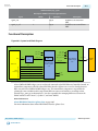
Functional Description............................................................................................................................... 2-1
Avalon-MM Interface......................................................................................................................2-2
Off-Chip SDRAM Interface............................................................................................................2-2
Board Layout and Pinout Considerations.................................................................................... 2-3
Performance Considerations..........................................................................................................2-4
Configuration............................................................................................................................................... 2-4
Memory Profile Page....................................................................................................................... 2-5
Timing Page...................................................................................................................................... 2-6
Hardware Simulation Considerations.......................................................................................................2-7
SDRAM Controller Simulation Model......................................................................................... 2-7
SDRAM Memory Model.................................................................................................................2-7
Example Configurations............................................................................................................................. 2-8
Software Programming Model...................................................................................................................2-9
Clock, PLL and Timing Considerations................................................................................................... 2-9
Factors Affecting SDRAM Timing.............................................................................................. 2-10
Symptoms of an Untuned PLL.....................................................................................................2-10
Estimating the Valid Signal Window.......................................................................................... 2-10
Example Calculation......................................................................................................................2-12
Document Revision History.....................................................................................................................2-14
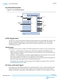
Tri-State SDRAM................................................................................................ 3-1
Feature Description..................................................................................................................................... 3-1
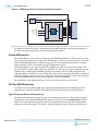
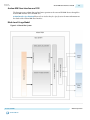
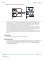
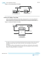
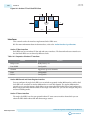
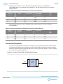
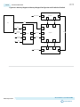
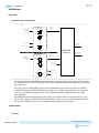
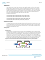
Block Diagram..................................................................................................................................3-2
Configuration Parameter............................................................................................................................ 3-2
Memory Profile Page....................................................................................................................... 3-2
Timing Page...................................................................................................................................... 3-2
Interface.........................................................................................................................................................3-3
Reset and Clock Requirements.................................................................................................................. 3-8
Architecture.................................................................................................................................................. 3-8
Avalon-MM Slave Interface and CSR........................................................................................... 3-9
Block Level Usage Model................................................................................................................ 3-9
Document Revision History.....................................................................................................................3-10
Altera Corporation
TOC-3
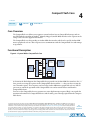
Compact Flash Core............................................................................................ 4-1
Core Overview..............................................................................................................................................4-1
Functional Description............................................................................................................................... 4-1
Required Connections.................................................................................................................................4-2
Software Programming Model...................................................................................................................4-3
HAL System Library Support......................................................................................................... 4-3
Software Files.................................................................................................................................... 4-3
Register Maps................................................................................................................................... 4-4
Document Revision History....................................................................................................................... 4-5
EPCS Serial Flash Controller Core..................................................................... 5-1
Core Overview..............................................................................................................................................5-1
Functional Description............................................................................................................................... 5-2
Avalon-MM Slave Interface and Registers................................................................................... 5-3
Configuration..............................................................................................................................................5-4
Software Programming Model...................................................................................................................5-4
HAL System Library Support......................................................................................................... 5-4
Software Files.................................................................................................................................... 5-4
Document Revision History....................................................................................................................... 5-5
JTAG UART Core................................................................................................6-1
Core Overview..............................................................................................................................................6-1
Functional Description............................................................................................................................... 6-1
Avalon Slave Interface and Registers.............................................................................................6-2
Read and Write FIFOs.....................................................................................................................6-2
JTAG Interface................................................................................................................................. 6-2
Host-Target Connection................................................................................................................. 6-2
Configuration............................................................................................................................................... 6-3
Configuration Page.......................................................................................................................... 6-3
Simulation Settings.......................................................................................................................... 6-4
Hardware Simulation Considerations.......................................................................................................6-5
Software Programming Model...................................................................................................................6-5
HAL System Library Support......................................................................................................... 6-5
Software Files.................................................................................................................................... 6-8
Accessing the JTAG UART Core via a Host PC..........................................................................6-9
Register Map..................................................................................................................................... 6-9
Interrupt Behavior......................................................................................................................... 6-10
Document Revision History.....................................................................................................................6-11
UART Core.......................................................................................................... 7-1
Core Overview..............................................................................................................................................7-1
Functional Description............................................................................................................................... 7-1
Avalon-MM Slave Interface and Registers................................................................................... 7-2
RS-232 Interface............................................................................................................................... 7-2
Altera Corporation
TOC-4
Transmitter Logic.............................................................................................................................7-2
Receiver Logic...................................................................................................................................7-2
Baud Rate Generation..................................................................................................................... 7-3
Instantiating the Core..................................................................................................................................7-3
Configuration Settings.................................................................................................................... 7-3
Simulation Settings.......................................................................................................................... 7-6
Simulation Considerations......................................................................................................................... 7-7
Software Programming Model...................................................................................................................7-8
HAL System Library Support......................................................................................................... 7-8
Software Files..................................................................................................................................7-11
Register Map...................................................................................................................................7-11
Interrupt Behavior......................................................................................................................... 7-16
Document Revision History.....................................................................................................................7-16
16550 UART........................................................................................................ 8-1
Core Overview..............................................................................................................................................8-1
Feature Description..................................................................................................................................... 8-1
Unsupported Features..................................................................................................................... 8-2
Interface.............................................................................................................................................8-2
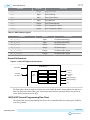
General Architecture....................................................................................................................... 8-4
16550 UART General Programming Flow Chart........................................................................8-4
Configuration Parameters.............................................................................................................. 8-6
DMA Support................................................................................................................................... 8-6
FPGA Resource Usage.....................................................................................................................8-7
Timing and Fmax.............................................................................................................................8-8
Avalon-MM Slave............................................................................................................................ 8-8
Overrun/Underrun Conditions..................................................................................................... 8-9
Hardware Auto Flow-Control......................................................................................................8-10
Clock and Baud Rate Selection.................................................................................................... 8-11
Software Programming Model.................................................................................................................8-11
Overview......................................................................................................................................... 8-11
Supported Features........................................................................................................................ 8-11
Unsupported Features...................................................................................................................8-12
Configuration................................................................................................................................. 8-12
16550 UART API........................................................................................................................... 8-13
Driver Examples.............................................................................................................................8-17
Address Map and Register Descriptions ............................................................................................... 8-21
rbr_thr_dll.......................................................................................................................................8-22
ier_dlh..............................................................................................................................................8-24
iir...................................................................................................................................................... 8-26
fcr......................................................................................................................................................8-27
lcr......................................................................................................................................................8-29
mcr................................................................................................................................................... 8-31
lsr...................................................................................................................................................... 8-33
msr................................................................................................................................................... 8-36
scr..................................................................................................................................................... 8-39
16550 UART Release Information.......................................................................................................... 8-39
Document Revision History.....................................................................................................................8-40
Altera Corporation
TOC-5
SPI Core............................................................................................................... 9-1
Core Overview..............................................................................................................................................9-1
Functional Description............................................................................................................................... 9-1
Example Configurations................................................................................................................. 9-2
Transmitter Logic.............................................................................................................................9-2
Receiver Logic...................................................................................................................................9-3
Master and Slave Modes..................................................................................................................9-3
Avalon-MM Interface......................................................................................................................9-5
Configuration............................................................................................................................................... 9-5
Master/Slave Settings.......................................................................................................................9-5
Data Register Settings......................................................................................................................9-6
Timing Settings................................................................................................................................ 9-6
Software Programming Model...................................................................................................................9-7
Hardware Access Routines............................................................................................................. 9-7
Software Files.................................................................................................................................... 9-8
Register Map..................................................................................................................................... 9-9
Document Revision History.....................................................................................................................9-11
Optrex 16207 LCD Controller Core..................................................................10-1
Core Overview............................................................................................................................................10-1
Functional Description............................................................................................................................. 10-1
Software Programming Model.................................................................................................................10-2
HAL System Library Support.......................................................................................................10-2
Displaying Characters on the LCD..............................................................................................10-2
Software Files..................................................................................................................................10-3
Register Map...................................................................................................................................10-3
Interrupt Behavior......................................................................................................................... 10-3
Document Revision History.....................................................................................................................10-3
PIO Core............................................................................................................ 11-1
Core Overview............................................................................................................................................11-1
Functional Description............................................................................................................................. 11-1
Data Input and Output................................................................................................................. 11-2
Edge Capture.................................................................................................................................. 11-2
IRQ Generation..............................................................................................................................11-2
Example Configurations........................................................................................................................... 11-3
Avalon-MM Interface....................................................................................................................11-3
Configuration............................................................................................................................................. 11-3
Basic Settings.................................................................................................................................. 11-3
Input Options................................................................................................................................. 11-4
Simulation....................................................................................................................................... 11-5
Software Programming Model.................................................................................................................11-5
Software Files..................................................................................................................................11-5
Register Map...................................................................................................................................11-5
Interrupt Behavior......................................................................................................................... 11-7
Altera Corporation
TOC-6
Software Files..................................................................................................................................11-8
Document Revision History.....................................................................................................................11-8
Avalon-ST Serial Peripheral Interface Core..................................................... 12-1
Core Overview............................................................................................................................................12-1
Functional Description............................................................................................................................. 12-1
Interfaces......................................................................................................................................... 12-1
Operation........................................................................................................................................ 12-2
Timing............................................................................................................................................. 12-2
Limitations...................................................................................................................................... 12-3
Configuration............................................................................................................................................. 12-3
Document Revision History.....................................................................................................................12-3
PCI Lite Core..................................................................................................... 13-1
Core Overview............................................................................................................................................13-1
Performance and Resource Utilization...................................................................................................13-1
Functional Description............................................................................................................................. 13-2
PCI-Avalon Bridge Blocks............................................................................................................ 13-2
Avalon-MM Ports..........................................................................................................................13-3
Prefetchable Avalon-MM Master................................................................................................ 13-3
Non-Prefectchable Avalon-MM Master.....................................................................................13-3
I/O Avalon-MM Master................................................................................................................13-4
PCI Bus Access Slave..................................................................................................................... 13-4
Control Register Access (CRA) Avalon-MM Slave...................................................................13-4
Master and Target Performance.................................................................................................. 13-5
PCI-to-Avalon Address Translation........................................................................................... 13-5
Avalon-to-PCI Address Translation........................................................................................... 13-6
Avalon-To-PCI Read and Write Operation...............................................................................13-7
Ordering of Requests.....................................................................................................................13-9
PCI Interrupt................................................................................................................................ 13-10
Configuration........................................................................................................................................... 13-10
PCI Timing Constraint Files...................................................................................................... 13-12
Simulation Considerations..................................................................................................................... 13-13
Master Transactor (mstr_tranx)................................................................................................13-13
Simulation Flow........................................................................................................................... 13-14
Document Revision History...................................................................................................................13-16
Avalon-ST Single-Clock and Dual-Clock FIFO Cores..................................... 14-1
Avalon-ST Single-Clock and Dual-Clock FIFO Cores.........................................................................14-1
Core Overview................................................................................................................................14-1
Functional Description............................................................................................................................. 14-1
Interfaces......................................................................................................................................... 14-2
Operating Modes........................................................................................................................... 14-3
Fill Level.......................................................................................................................................... 14-3
Thresholds.......................................................................................................................................14-3
Parameters.................................................................................................................................................. 14-4
Altera Corporation
TOC-7
Register Description.................................................................................................................................. 14-5
Document Revision History.....................................................................................................................14-6
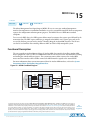
MDIO Core........................................................................................................ 15-1
Functional Description............................................................................................................................. 15-1
MDIO Frame Format (Clause 45)............................................................................................... 15-2
MDIO Clock Generation.............................................................................................................. 15-3
Interfaces......................................................................................................................................... 15-3
Operation........................................................................................................................................ 15-3
Parameter.................................................................................................................................................... 15-4
Configuration Registers............................................................................................................................ 15-4
Document Revision History.....................................................................................................................15-5
On-Chip FIFO Memory Core............................................................................16-1
Core Overview............................................................................................................................................16-1
Functional Description............................................................................................................................. 16-1
Avalon-MM Write Slave to Avalon-MM Read Slave............................................................... 16-1
Avalon-ST Sink to Avalon-ST Source.........................................................................................16-2
Avalon-MM Write Slave to Avalon-ST Source......................................................................... 16-2
Avalon-ST Sink to Avalon-MM Read Slave...............................................................................16-4
Status Interface............................................................................................................................... 16-5
Clocking Modes............................................................................................................................. 16-5
Configuration............................................................................................................................................. 16-5
FIFO Settings.................................................................................................................................. 16-5
Interface Parameters......................................................................................................................16-6
Software Programming Model.................................................................................................................16-7
HAL System Library Support.......................................................................................................16-7
Software Files..................................................................................................................................16-7
Programming with the On-Chip FIFO Memory...................................................................................16-7
Software Control............................................................................................................................ 16-8
Software Example........................................................................................................................ 16-11
On-Chip FIFO Memory API..................................................................................................................16-12
altera_avalon_fifo_init()............................................................................................................. 16-12
altera_avalon_fifo_read_status()............................................................................................... 16-12
altera_avalon_fifo_read_ienable().............................................................................................16-13
altera_avalon_fifo_read_almostfull()........................................................................................16-13
altera_avalon_fifo_read_almostempty().................................................................................. 16-13
altera_avalon_fifo_read_event()................................................................................................16-14
altera_avalon_fifo_read_level()................................................................................................. 16-14
altera_avalon_fifo_clear_event()............................................................................................... 16-14
altera_avalon_fifo_write_ienable()........................................................................................... 16-15
altera_avalon_fifo_write_almostfull()...................................................................................... 16-15
altera_avalon_fifo_write_almostempty()................................................................................. 16-15
altera_avalon_write_fifo().......................................................................................................... 16-16
altera_avalon_write_other_info()............................................................................................. 16-16
altera_avalon_fifo_read_fifo()................................................................................................... 16-17
Document Revision History...................................................................................................................16-17
Altera Corporation
TOC-8
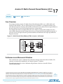
Avalon-ST Multi-Channel Shared Memory FIFO Core................................... 17-1
Core Overview............................................................................................................................................17-1
Performance and Resource Utilization...................................................................................................17-1
Functional Description............................................................................................................................. 17-3
Interfaces......................................................................................................................................... 17-3
Operation........................................................................................................................................ 17-4
Parameters.................................................................................................................................................. 17-4
Software Programming Model.................................................................................................................17-6
HAL System Library Support.......................................................................................................17-6
Register Map...................................................................................................................................17-6
Document Revision History.....................................................................................................................17-8
SPI Slave/JTAG to Avalon Master Bridge Cores.............................................. 18-1
Core Overview............................................................................................................................................18-1
Functional Description............................................................................................................................. 18-1
Parameters.................................................................................................................................................. 18-3
Document Revision History.....................................................................................................................18-3
Avalon Streaming Channel Multiplexer and Demultiplexer Cores.................19-1
Avalon Streaming Channel Multiplexer and Demultiplexer Cores................................................... 19-1
Core Overview............................................................................................................................................19-1
Resource Usage and Performance............................................................................................... 19-1
Multiplexer..................................................................................................................................................19-2
Functional Description................................................................................................................. 19-2
Parameters...................................................................................................................................... 19-3
Demultiplexer.............................................................................................................................................19-4
Functional Description................................................................................................................. 19-4
Parameters...................................................................................................................................... 19-5
Hardware Simulation Considerations.................................................................................................... 19-6
Software Programming Model.................................................................................................................19-6
Document Revision History.....................................................................................................................19-7
Avalon-ST Bytes to Packets and Packets to Bytes Converter Cores................ 20-1
Functional Description............................................................................................................................. 20-1
Interfaces......................................................................................................................................... 20-2
Operation—Avalon-ST Bytes to Packets Converter Core....................................................... 20-2
Operation—Avalon-ST Packets to Bytes Converter Core....................................................... 20-3
Document Revision History.....................................................................................................................20-3
Avalon Packets to Transactions Converter Core..............................................21-1
Core Overview............................................................................................................................................21-1
Functional Description............................................................................................................................. 21-1
Interfaces......................................................................................................................................... 21-1
Operation........................................................................................................................................ 21-2
Altera Corporation
TOC-9
Document Revision History.....................................................................................................................21-3
Avalon-ST Round Robin Scheduler Core......................................................... 22-1
Avalon-ST Round Robin Scheduler Core.............................................................................................. 22-1
Core Overview............................................................................................................................................22-1
Performance and Resource Utilization...................................................................................................22-1
Functional Description............................................................................................................................. 22-2
Interfaces......................................................................................................................................... 22-3
Operations.......................................................................................................................................22-3
Parameters.................................................................................................................................................. 22-4
Document Revision History.....................................................................................................................22-4
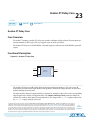
Avalon-ST Delay Core....................................................................................... 23-1
Avalon-ST Delay Core.............................................................................................................................. 23-1
Core Overview............................................................................................................................................23-1
Functional Description............................................................................................................................. 23-1
Reset.................................................................................................................................................23-2
Interfaces......................................................................................................................................... 23-2
Parameters.................................................................................................................................................. 23-2
Document Revision History.....................................................................................................................23-4
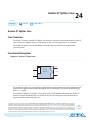
Avalon-ST Splitter Core.................................................................................... 24-1
Avalon-ST Splitter Core............................................................................................................................24-1
Core Overview............................................................................................................................................24-1
Functional Description............................................................................................................................. 24-1
Backpressure................................................................................................................................... 24-2
Interfaces......................................................................................................................................... 24-2
Parameters.................................................................................................................................................. 24-2
Document Revision History.....................................................................................................................24-4
Scatter-Gather DMA Controller Core.............................................................. 25-1
Core Overview............................................................................................................................................25-1
Example Systems............................................................................................................................25-1
Comparison of SG-DMA Controller Core and DMA Controller Core.................................25-2
Resource Usage and Performance........................................................................................................... 25-2
Functional Description............................................................................................................................. 25-3
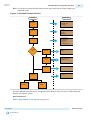
Functional Blocks and Configurations....................................................................................... 25-3
DMA Descriptors...........................................................................................................................25-6
Error Conditions............................................................................................................................25-7
Parameters.................................................................................................................................................. 25-9
Simulation Considerations....................................................................................................................... 25-9
Software Programming Model...............................................................................................................25-10
HAL System Library Support.....................................................................................................25-10
Software Files................................................................................................................................25-10
Register Maps............................................................................................................................... 25-10
Altera Corporation
TOC-10
DMA Descriptors.........................................................................................................................25-14
Timeouts....................................................................................................................................... 25-16
Programming with SG-DMA Controller............................................................................................. 25-16
Data Structure.............................................................................................................................. 25-16
SG-DMA API............................................................................................................................... 25-17
alt_avalon_sgdma_do_async_transfer()...................................................................................25-18
alt_avalon_sgdma_do_sync_transfer().....................................................................................25-18
alt_avalon_sgdma_construct_mem_to_mem_desc()............................................................ 25-19
alt_avalon_sgdma_construct_stream_to_mem_desc()..........................................................25-20
alt_avalon_sgdma_construct_mem_to_stream_desc()..........................................................25-21
alt_avalon_sgdma_enable_desc_poll().....................................................................................25-22
alt_avalon_sgdma_disable_desc_poll().................................................................................... 25-23
alt_avalon_sgdma_check_descriptor_status().........................................................................25-23
alt_avalon_sgdma_register_callback()......................................................................................25-23
alt_avalon_sgdma_start()........................................................................................................... 25-24
alt_avalon_sgdma_stop()............................................................................................................25-24
alt_avalon_sgdma_open().......................................................................................................... 25-25
Document Revision History...................................................................................................................25-25
Altera Modular Scatter-Gather DMA............................................................... 26-1
Overview..................................................................................................................................................... 26-1
Feature Description................................................................................................................................... 26-1
mSGDMA Interfaces and Parameters.........................................................................................26-4
mSGDMA Descriptors..................................................................................................................26-8
Programming Model................................................................................................................... 26-13
Register Map of mSGDMA........................................................................................................ 26-14
Modular Scatter-Gather DMA Prefetcher Core.................................................................................. 26-17
Feature Description..................................................................................................................... 26-17
Functional Description............................................................................................................... 26-17
Driver Implementation........................................................................................................................... 26-33
alt_msgdma_standard_descriptor_async_transfer.................................................................26-33
alt_msgdma_extended_descriptor_async_transfer................................................................ 26-34
alt_msgdma_descriptor_async_transfer...................................................................................26-35
alt_msgdma_standard_descriptor_sync_transfer...................................................................26-36
alt_msgdma_extended_descriptor_sync_transfer.................................................................. 26-37
alt_msgdma_descriptor_sync_transfer.................................................................................... 26-38
alt_msgdma_construct_standard_st_to_mm_descriptor......................................................26-39
alt_msgdma_construct_standard_mm_to_st_descriptor......................................................26-40
alt_msgdma_construct_standard_mm_to_mm_descriptor................................................. 26-41
alt_msgdma_construct_standard_descriptor.......................................................................... 26-42
alt_msgdma_construct_extended_st_to_mm_descriptor..................................................... 26-43
alt_msgdma_construct_extended_mm_to_st_descriptor..................................................... 26-44
alt_msgdma_construct_extended_mm_to_mm_descriptor.................................................26-45
alt_msgdma_construct_extended_descriptor......................................................................... 26-46
alt_msgdma_register_callback...................................................................................................26-47
alt_msgdma_open........................................................................................................................26-48
alt_msgdma_write_standard_descriptor..................................................................................26-49
alt_msgdma_write_extended_descriptor................................................................................. 26-50
Altera Corporation
TOC-11
alt_avalon_msgdma_init............................................................................................................ 26-51
Document Revision History...................................................................................................................26-52
DMA Controller Core....................................................................................... 27-1
Core Overview............................................................................................................................................27-1
Functional Description............................................................................................................................. 27-1
Setting Up DMA Transactions.....................................................................................................27-2
The Master Read and Write Ports............................................................................................... 27-2
Addressing and Address Incrementing...................................................................................... 27-3
Parameters.................................................................................................................................................. 27-3
DMA Parameters (Basic).............................................................................................................. 27-3
Advanced Options......................................................................................................................... 27-4
Software Programming Model.................................................................................................................27-5
HAL System Library Support.......................................................................................................27-5
Software Files..................................................................................................................................27-6
Register Map...................................................................................................................................27-6
Interrupt Behavior......................................................................................................................... 27-9
Document Revision History...................................................................................................................27-10
Video Sync Generator and Pixel Converter Cores........................................... 28-1
Core Overview............................................................................................................................................28-1
Video Sync Generator............................................................................................................................... 28-1
Functional Description................................................................................................................. 28-1
Parameters...................................................................................................................................... 28-2
Signals.............................................................................................................................................. 28-3
Timing Diagrams........................................................................................................................... 28-4
Pixel Converter...........................................................................................................................................28-5
Functional Description................................................................................................................. 28-5
Parameters...................................................................................................................................... 28-5
Signals.............................................................................................................................................. 28-5
Hardware Simulation Considerations.................................................................................................... 28-6
Document Revision History.....................................................................................................................28-6
Interval Timer Core...........................................................................................29-1
Core Overview............................................................................................................................................29-1
Functional Description............................................................................................................................. 29-1
Avalon-MM Slave Interface..........................................................................................................29-2
Configuration............................................................................................................................................. 29-2
Timeout Period.............................................................................................................................. 29-2
Counter Size....................................................................................................................................29-3
Hardware Options......................................................................................................................... 29-3
Configuring the Timer as a Watchdog Timer........................................................................... 29-4
Software Programming Model.................................................................................................................29-4
HAL System Library Support.......................................................................................................29-4
Software Files..................................................................................................................................29-5
Register Map...................................................................................................................................29-5
Altera Corporation
TOC-12
Interrupt Behavior......................................................................................................................... 29-8
Document Revision History.....................................................................................................................29-8
Mutex Core........................................................................................................ 30-1
Core Overview............................................................................................................................................30-1
Functional Description............................................................................................................................. 30-1
Configuration............................................................................................................................................. 30-2
Software Programming Model.................................................................................................................30-2
Software Files..................................................................................................................................30-2
Hardware Access Routines........................................................................................................... 30-2
Mutex API...................................................................................................................................................30-3
altera_avalon_mutex_is_mine().................................................................................................. 30-3
altera_avalon_mutex_first_lock()............................................................................................... 30-3
altera_avalon_mutex_lock().........................................................................................................30-4
altera_avalon_mutex_open()....................................................................................................... 30-4
altera_avalon_mutex_trylock()....................................................................................................30-4
altera_avalon_mutex_unlock().................................................................................................... 30-5
Document Revision History.....................................................................................................................30-5
Vectored Interrupt Controller Core................................................................. 31-1
Core Overview............................................................................................................................................31-1
Functional Description............................................................................................................................. 31-3
External Interfaces......................................................................................................................... 31-3
Functional Blocks...........................................................................................................................31-4
Register Maps............................................................................................................................................. 31-6
Parameters................................................................................................................................................ 31-11
Altera HAL Software Programming Model......................................................................................... 31-12
Software Files................................................................................................................................31-12
Macros........................................................................................................................................... 31-12
Data Structure.............................................................................................................................. 31-13
VIC API.........................................................................................................................................31-13
Run-time Initialization................................................................................................................31-16
Board Support Package............................................................................................................... 31-16
Document Revision History...................................................................................................................31-22
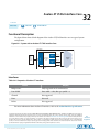
Avalon-ST JTAG Interface Core....................................................................... 32-1
Functional Description............................................................................................................................. 32-1
Interfaces......................................................................................................................................... 32-1
Core Behavior.................................................................................................................................32-2
Parameters...................................................................................................................................... 32-3
Document Revision History.....................................................................................................................32-3
System ID Core.................................................................................................. 33-1
Core Overview............................................................................................................................................33-1
Functional Description............................................................................................................................. 33-1
Altera Corporation
TOC-13
Configuration............................................................................................................................................. 33-2
Software Programming Model.................................................................................................................33-2
alt_avalon_sysid_test()..................................................................................................................33-2
Document Revision History.....................................................................................................................33-2
Performance Counter Core............................................................................... 34-1
Core Overview............................................................................................................................................34-1
Functional Description............................................................................................................................. 34-1
Section Counters............................................................................................................................ 34-1
Global Counter...............................................................................................................................34-2
Register Map...................................................................................................................................34-2
System Reset................................................................................................................................... 34-3
Configuration............................................................................................................................................. 34-3
Define Counters............................................................................................................................. 34-3
Multiple Clock Domain Considerations.....................................................................................34-3
Hardware Simulation Considerations.................................................................................................... 34-3
Software Programming Model.................................................................................................................34-3
Software Files..................................................................................................................................34-3
Using the Performance Counter..................................................................................................34-3
Interrupt Behavior......................................................................................................................... 34-6
Performance Counter API........................................................................................................................34-6
PERF_RESET()...............................................................................................................................34-6
PERF_START_MEASURING().................................................................................................. 34-6
PERF_STOP_MEASURING()..................................................................................................... 34-7
PERF_BEGIN().............................................................................................................................. 34-7
PERF_END().................................................................................................................................. 34-7
perf_print_formatted_report().................................................................................................... 34-8
perf_get_total_time().................................................................................................................... 34-8
perf_get_section_time()................................................................................................................34-9
perf_get_num_starts()...................................................................................................................34-9
alt_get_cpu_freq()....................................................................................................................... 34-10
Document Revision History...................................................................................................................34-10
Avalon Streaming Test Pattern Generator and Checker Cores....................... 35-1
Avalon Streaming Test Pattern Generator and Checker Cores.......................................................... 35-1
Core Overview................................................................................................................................35-1
Resource Utilization and Performance...................................................................................................35-1
Test Pattern Generator..............................................................................................................................35-2
Functional Description................................................................................................................. 35-2
Configuration................................................................................................................................. 35-3
Test Pattern Checker................................................................................................................................. 35-4
Functional Description................................................................................................................. 35-4
Configuration................................................................................................................................. 35-5
Hardware Simulation Considerations.................................................................................................... 35-6
Software Programming Model.................................................................................................................35-6
HAL System Library Support.......................................................................................................35-6
Software Files..................................................................................................................................35-6
Altera Corporation
TOC-14
Register Maps................................................................................................................................. 35-6
Test Pattern Generator API....................................................................................................................35-10
data_source_reset()..................................................................................................................... 35-10
data_source_init()........................................................................................................................35-11
data_source_get_id()...................................................................................................................35-11
data_source_get_supports_packets()........................................................................................35-11
data_source_get_num_channels()............................................................................................ 35-11
data_source_get_symbols_per_cycle()..................................................................................... 35-12
data_source_set_enable()........................................................................................................... 35-12
data_source_get_enable()...........................................................................................................35-12
data_source_set_throttle()..........................................................................................................35-13
data_source_get_throttle()......................................................................................................... 35-13
data_source_is_busy().................................................................................................................35-13
data_source_fill_level()...............................................................................................................35-13
data_source_send_data()............................................................................................................35-14
Test Pattern Checker API....................................................................................................................... 35-14
data_sink_reset()..........................................................................................................................35-14
data_sink_init()............................................................................................................................35-15
data_sink_get_id()....................................................................................................................... 35-15
data_sink_get_supports_packets()............................................................................................35-15
data_sink_get_num_channels()................................................................................................ 35-16
data_sink_get_symbols_per_cycle()......................................................................................... 35-16
data_sink_set enable().................................................................................................................35-16
data_sink_get_enable()............................................................................................................... 35-16
data_sink_set_throttle()..............................................................................................................35-17
data_sink_get_throttle()............................................................................................................. 35-17
data_sink_get_packet_count()...................................................................................................35-17
data_sink_get_symbol_count()................................................................................................. 35-17
data_sink_get_error_count()..................................................................................................... 35-18
data_sink_get_exception()......................................................................................................... 35-18
data_sink_exception_is_exception().........................................................................................35-18
data_sink_exception_has_data_error()....................................................................................35-19
data_sink_exception_has_missing_sop().................................................................................35-19
data_sink_exception_has_missing_eop()................................................................................ 35-19
data_sink_exception_signalled_error()....................................................................................35-19
data_sink_exception_channel().................................................................................................35-20
Document Revision History...................................................................................................................35-20
Avalon Streaming Data Pattern Generator and Checker Cores...................... 36-1
Avalon Streaming Data Pattern Generator and Checker Cores..........................................................36-1
Data Pattern Generator.............................................................................................................................36-1
Functional Description................................................................................................................. 36-1
Configuration................................................................................................................................. 36-3
Data Pattern Checker................................................................................................................................ 36-3
Functional Description................................................................................................................. 36-3
Configuration................................................................................................................................. 36-5
Hardware Simulation Considerations.................................................................................................... 36-5
Software Programming Model.................................................................................................................36-5
Altera Corporation
TOC-15
Register Maps................................................................................................................................. 36-5
Document Revision History...................................................................................................................36-10
PLL Cores...........................................................................................................37-1
Core Overview............................................................................................................................................37-1
Functional Description............................................................................................................................. 37-2
ALTPLL Megafunction................................................................................................................. 37-2
Clock Outputs................................................................................................................................ 37-2
PLL Status and Control Signals....................................................................................................37-2
System Reset Considerations........................................................................................................37-3
Instantiating the Avalon ALTPLL Core..................................................................................................37-3
Instantiating the PLL Core....................................................................................................................... 37-3
Hardware Simulation Considerations.................................................................................................... 37-4
Register Definitions and Bit List..............................................................................................................37-5
Status Register................................................................................................................................ 37-5
Control Register............................................................................................................................. 37-6
Phase Reconfig Control Register................................................................................................. 37-6
Document Revision History.....................................................................................................................37-7
Altera MSI to GIC Generator............................................................................38-1
Overview..................................................................................................................................................... 38-1
Background.................................................................................................................................................38-1
Feature Description................................................................................................................................... 38-1
Interrupt Servicing Process.......................................................................................................... 38-2
Registers of Component................................................................................................................38-3
Unsupported Feature.................................................................................................................... 38-4
Document Revision History.....................................................................................................................38-5
Altera Interrupt Latency Counter.....................................................................39-1
Overview..................................................................................................................................................... 39-1
Feature Description................................................................................................................................... 39-2
Avalon-MM Compliant CSR Registers.......................................................................................39-2
32-bit Counter................................................................................................................................ 39-4
Interrupt Detector..........................................................................................................................39-5
Component Interface................................................................................................................................ 39-5
Component Parameterization..................................................................................................................39-5
Software Access.......................................................................................................................................... 39-6
Routine for Level Sensitive Interrupts........................................................................................ 39-6
Routine for Edge/Pulse Sensitive Interrupts.............................................................................. 39-6
Implementation Details............................................................................................................................ 39-7
Interrupt Latency Counter Architecture.................................................................................... 39-7
IP Caveats....................................................................................................................................................39-8
Document Revision History.....................................................................................................................39-8
Altera GMII to RGMII Adapter........................................................................40-1
Altera Corporation
TOC-16
Overview..................................................................................................................................................... 40-1
Feature Description................................................................................................................................... 40-1
Supported Features........................................................................................................................ 40-1
Unsupported Features...................................................................................................................40-1
Parameters.................................................................................................................................................. 40-2
IP Configuration Parameter......................................................................................................... 40-2
Altera GMII to RGMII Adapter Core Interface.................................................................................... 40-2
Functional Description............................................................................................................................. 40-5
Architecture.................................................................................................................................... 40-6
Altera HPS EMAC Interface Splitter Core............................................................................................. 40-7
Parameter........................................................................................................................................ 40-7
Document Revision History...................................................................................................................40-14
Altera Generic Quad SPI Controller.................................................................41-1
Overview..................................................................................................................................................... 41-1
Functional Description............................................................................................................................. 41-1
Parameters.................................................................................................................................................. 41-2
Configuration Device Types.........................................................................................................41-2
I/O Mode.........................................................................................................................................41-2
Chip Selects.....................................................................................................................................41-2
Interface Signals............................................................................................................................. 41-2
Registers...................................................................................................................................................... 41-5
Register Memory Map...................................................................................................................41-5
Register Descriptions.....................................................................................................................41-5
Valid Sector Combination for Sector Protect and Sector Erase Command........................ 41-10
Nios II Tools Support..............................................................................................................................41-11
Booting Nios II from Flash.........................................................................................................41-11
Nios II HAL Driver......................................................................................................................41-13
Document Revision History...................................................................................................................41-13
Altera Serial Flash Controller........................................................................... 42-1
Overview..................................................................................................................................................... 42-1
Functional Description............................................................................................................................. 42-1
Parameters.................................................................................................................................................. 42-2
Configuration Device Types.........................................................................................................42-2
I/O Mode.........................................................................................................................................42-2
Chip Selects.....................................................................................................................................42-2
Interface Signals............................................................................................................................. 42-2
Registers...................................................................................................................................................... 42-5
Register Memory Map...................................................................................................................42-5
Register Descriptions.....................................................................................................................42-5
Valid Sector Combination for Sector Protect and Sector Erase Command........................ 42-10
Nios II Tools Support..............................................................................................................................42-11
Booting Nios II from Flash.........................................................................................................42-11
Nios II HAL Driver......................................................................................................................42-13
Document Revision History...................................................................................................................42-13
Altera Corporation
TOC-17
Altera Avalon Mailbox (simple)........................................................................43-1
Overview..................................................................................................................................................... 43-1
Functional Description............................................................................................................................. 43-1
Message Sending and Retrieval Process......................................................................................43-2
Registers of Component................................................................................................................43-2
Interface.......................................................................................................................................................43-4
Component Interface.................................................................................................................... 43-4
Component Parameterization......................................................................................................43-5
HAL Driver................................................................................................................................................. 43-6
Feature Description....................................................................................................................... 43-6
Document Revision History...................................................................................................................43-11
Document Revision History............................................................................... A-1
Altera Corporation
1
Embedded IP Peripherals User Guide
Introduction
2014.07.24
UG-01085
Subscribe
Send Feedback
This user guide describes the IP cores provided by Altera® that are included in the Quartus® II design
software.
The IP cores are optimized for Altera devices and can be easily implemented to reduce design and test
time. You can use the IP parameter editor from Qsys to add the IP cores to your system, configure the
cores, and specify their connectivity.
Altera's Qsys system integration tool is available in the Quartus II software subcription edition version
15.0.
Before using Qsys, review the (Quartus II software Version 15.0 Release Notes) for known issues and
limitations. To submit general feedback or technical support, click Feedback on the Quartus II software
Help menu and also on all Altera technical documentation.
Related Information
•
•
•
•
Quartus II Handbook Volume 1: Design and Synthesis
Quartus II Handbook Volume 2: Design Implementation and Optimization
Quartus II Handbook Volume 3: Verification
Quartus II Software and Device Support Release Notes Version 15.0
Tool Support
Qsys is a system-level integration tool which is included as part of the Quartus II software. Qsys leverages
the easy-to-use interface of SOPC Builder and provides backward compatibility for easy migration of
existing embedded systems.You can implement a design using the IP cores from the Qsys component
library.
All the IP cores described in this user guide are supported by Qsys except for the following cores which
are only supported by SOPC Builder.
• Common Flash Interface Controller Core
• SDRAM Controller Core (pin-sharing mode)
• System ID Core
Obsolescence
The following IP cores are scheduled for product obsolescence and discontinued support:
© 2015 Altera Corporation. All rights reserved. ALTERA, ARRIA, CYCLONE, ENPIRION, MAX, MEGACORE, NIOS, QUARTUS and STRATIX words and logos are
trademarks of Altera Corporation and registered in the U.S. Patent and Trademark Office and in other countries. All other words and logos identified as
trademarks or service marks are the property of their respective holders as described at www.altera.com/common/legal.html. Altera warrants performance
of its semiconductor products to current specifications in accordance with Altera's standard warranty, but reserves the right to make changes to any
products and services at any time without notice. Altera assumes no responsibility or liability arising out of the application or use of any information,
product, or service described herein except as expressly agreed to in writing by Altera. Altera customers are advised to obtain the latest version of device
specifications before relying on any published information and before placing orders for products or services.
www.altera.com
101 Innovation Drive, San Jose, CA 95134
ISO
9001:2008
Registered
1-2
UG-01085
2014.07.24
Device Support
• PCI Lite Core
• Mailbox Core
Altera recommends that you do not use these cores in new designs.
For more information about Altera’s current IP offering, refer to Altera’s Intellectual Property website.
Related Information
Altera's Intellectual Property
Device Support
The IP cores described in this user guide support all Altera device families except the cores listed in the
table below.
Table 1-1: Device Support
IP Cores
Device Support
Off-Chip Interfaces
EPCS Serial Flash Controller Core
All device families except HardCopy® series.
On-Chip Interfaces
On-Chip FIFO Memory Core
All device families except HardCopy series.
Different device families support different I/O standards, which may affect the ability of the core to
interface to certain components. For details about supported I/O types, refer to the device handbook for
the target device family.
Document Revision History
Table 1-2: Document Revision History
Date
Version
Changes
June 2015
2015.06.12
Updated for 15.0
July 2014
2014.07.24
Removed mention of SOPC Builder, updated to Qsys
December 2013
v13.1.0
Removed listing of the DMA Controller core in the Qsys unsupported
list. The DMA controller core is now supported in Qsys.
Removed listing of the MDIO core in Device Support Table. The
MDIO core support all device families that the 10-Gbps Ethernet
MAC MegaCore Function supports.
December 2010
Altera Corporation
v10.1.0
Initial release.
Embedded IP Peripherals User Guide Introduction
Send Feedback
2
SDRAM Controller Core
2014.07.24
UG-01085
Subscribe
Send Feedback
Core Overview
The SDRAM controller core with Avalon ®interface provides an Avalon Memory-Mapped (Avalon-MM)
interface to off-chip SDRAM. The SDRAM controller allows designers to create custom systems in an
Altera device that connect easily to SDRAM chips. The SDRAM controller supports standard SDRAM as
described in the PC100 specification.
SDRAM is commonly used in cost-sensitive applications requiring large amounts of volatile memory.
While SDRAM is relatively inexpensive, control logic is required to perform refresh operations, open-row
management, and other delays and command sequences. The SDRAM controller connects to one or more
SDRAM chips, and handles all SDRAM protocol requirements. Internal to the device, the core presents an
Avalon-MM slave port that appears as linear memory (flat address space) to Avalon-MM master
peripherals.
The core can access SDRAM subsystems with various data widths (8, 16, 32, or 64 bits), various memory
sizes, and multiple chip selects. The Avalon-MM interface is latency-aware, allowing read transfers to be
pipelined. The core can optionally share its address and data buses with other off-chip Avalon-MM tristate devices. This feature is valuable in systems that have limited I/O pins, yet must connect to multiple
memory chips in addition to SDRAM.
Functional Description
The diagram below shows a block diagram of the SDRAM controller core connected to an external
SDRAM chip.
© 2015 Altera Corporation. All rights reserved. ALTERA, ARRIA, CYCLONE, ENPIRION, MAX, MEGACORE, NIOS, QUARTUS and STRATIX words and logos are
trademarks of Altera Corporation and registered in the U.S. Patent and Trademark Office and in other countries. All other words and logos identified as
trademarks or service marks are the property of their respective holders as described at www.altera.com/common/legal.html. Altera warrants performance
of its semiconductor products to current specifications in accordance with Altera's standard warranty, but reserves the right to make changes to any
products and services at any time without notice. Altera assumes no responsibility or liability arising out of the application or use of any information,
product, or service described herein except as expressly agreed to in writing by Altera. Altera customers are advised to obtain the latest version of device
specifications before relying on any published information and before placing orders for products or services.
www.altera.com
101 Innovation Drive, San Jose, CA 95134
ISO
9001:2008
Registered
2-2
UG-01085
2014.07.24
Avalon-MM Interface
Figure 2-1: SDRAM Controller with Avalon Interface Block Diagram
Altera FPGA
Clock
Source
PLL
SDRAM Clock
Phase Shift
Controller Clock
Avalon-MM slave
interface
to on-chip
logic
address
data, control
waitrequest
readdatavalid
Control
Logic
SDRAM Chip
(PC100)
Interface to SDRAM pins
clock
Avalon-MM Slave Port
SDRAM Controller Core
clk
cke
addr
ba
cs
cas
ras
we
dq
dqm
The following sections describe the components of the SDRAM controller core in detail. All options are
specified at system generation time, and cannot be changed at runtime.
Avalon-MM Interface
The Avalon-MM slave port is the user-visible part of the SDRAM controller core. The slave port presents
a flat, contiguous memory space as large as the SDRAM chip(s). When accessing the slave port, the details
of the PC100 SDRAM protocol are entirely transparent. The Avalon-MM interface behaves as a simple
memory interface. There are no memory-mapped configuration registers.
The Avalon-MM slave port supports peripheral-controlled wait states for read and write transfers. The
slave port stalls the transfer until it can present valid data. The slave port also supports read transfers with
variable latency, enabling high-bandwidth, pipelined read transfers. When a master peripheral reads
sequential addresses from the slave port, the first data returns after an initial period of latency. Subsequent
reads can produce new data every clock cycle. However, data is not guaranteed to return every clock cycle,
because the SDRAM controller must pause periodically to refresh the SDRAM.
For details about Avalon-MM transfer types, refer to the Avalon Interface Specifications.
Off-Chip SDRAM Interface
The interface to the external SDRAM chip presents the signals defined by the PC100 standard. These
signals must be connected externally to the SDRAM chip(s) through I/O pins on the Altera device.
Signal Timing and Electrical Characteristics
The timing and sequencing of signals depends on the configuration of the core. The hardware designer
configures the core to match the SDRAM chip chosen for the system. See the Configuration section for
details. The electrical characteristics of the device pins depend on both the target device family and the
®
assignments made in the Quartus II software. Some device families support a wider range of electrical
Altera Corporation
SDRAM Controller Core
Send Feedback
UG-01085
2014.07.24
Synchronizing Clock and Data Signals
2-3
standards, and therefore are capable of interfacing with a greater variety of SDRAM chips. For details,
refer to the device handbook for the target device family.
Synchronizing Clock and Data Signals
The clock for the SDRAM chip (SDRAM clock) must be driven at the same frequency as the clock for the
Avalon-MM interface on the SDRAM controller (controller clock). As in all synchronous designs, you
must ensure that address, data, and control signals at the SDRAM pins are stable when a clock edge
arrives. As shown in the above SDRAM Controller with Avalon Interface block diagram, you can use an
on-chip phase-locked loop (PLL) to alleviate clock skew between the SDRAM controller core and the
SDRAM chip. At lower clock speeds, the PLL might not be necessary. At higher clock rates, a PLL is
necessary to ensure that the SDRAM clock toggles only when signals are stable on the pins. The PLL block
is not part of the SDRAM controller core. If a PLL is necessary, you must instantiate it manually. You can
instantiate the PLL core interface or instantiate an ALTPLL megafunction outside the Qsys system
module.
If you use a PLL, you must tune the PLL to introduce a clock phase shift so that SDRAM clock edges
arrive after synchronous signals have stabilized. See Clock, PLL and Timing Considerations sections for
details.
For more information about instantiating a PLL, refer to PLL Cores chapter. The Nios II development
tools provide example hardware designs that use the SDRAM controller core in conjunction with a PLL,
which you can use as a reference for your custom designs.
®
The Nios II development tools are available free for download from www.Altera.com.
Clock Enable (CKE) not Supported
The SDRAM controller does not support clock-disable modes. The SDRAM controller permanently
asserts the CKE signal on the SDRAM.
Sharing Pins with other Avalon-MM Tri-State Devices
If an Avalon-MM tri-state bridge is present, the SDRAM controller core can share pins with the existing
tri-state bridge. In this case, the core’s addr, dq (data) and dqm (byte-enable) pins are shared with other
devices connected to the Avalon-MM tri-state bridge. This feature conserves I/O pins, which is valuable in
systems that have multiple external memory chips (for example, flash, SRAM, and SDRAM), but too few
pins to dedicate to the SDRAM chip. See Performance Considerations section for details about how pin
sharing affects performance.
The SDRAM addresses must connect all address bits regardless of the size of the word so that the loworder address bits on the tri-state bridge align with the low-order address bits on the memory device. The
Avalon-MM tristate address signal always presents a byte address. It is not possible to drop A0 of the tristate bridge for memories when the smallest access size is 16 bits or A0-A1 of the tri-state bridge when the
smallest access size is 32 bits.
Board Layout and Pinout Considerations
When making decisions about the board layout and device pinout, try to minimize the skew between the
SDRAM signals. For example, when assigning the device pinout, group the SDRAM signals, including the
SDRAM clock output, physically close together. Also, you can use the Fast Input Register and Fast
Output Register logic options in the Quartus II software. These logic options place registers for the
SDRAM signals in the I/O cells. Signals driven from registers in I/O cells have similar timing characteris‐
tics, such as tCO, tSU, and tH.
SDRAM Controller Core
Send Feedback
Altera Corporation
2-4
UG-01085
2014.07.24
Performance Considerations
Performance Considerations
Under optimal conditions, the SDRAM controller core’s bandwidth approaches one word per clock cycle.
However, because of the overhead associated with refreshing the SDRAM, it is impossible to reach one
word per clock cycle. Other factors affect the core’s performance, as described in the following sections.
Open Row Management
SDRAM chips are arranged as multiple banks of memory, in which each bank is capable of independent
open-row address management. The SDRAM controller core takes advantage of open-row management
for a single bank. Continuous reads or writes within the same row and bank operate at rates approaching
one word per clock. Applications that frequently access different destination banks require extra
management cycles to open and close rows.
Sharing Data and Address Pins
When the controller shares pins with other tri-state devices, average access time usually increases and
bandwidth decreases. When access to the tri-state bridge is granted to other devices, the SDRAM incurs
overhead to open and close rows. Furthermore, the SDRAM controller has to wait several clock cycles
before it is granted access again.
To maximize bandwidth, the SDRAM controller automatically maintains control of the tri-state bridge as
long as back-to-back read or write transactions continue within the same row and bank.
This behavior may degrade the average access time for other devices sharing the Avalon-MM tri-state
bridge.
The SDRAM controller closes an open row whenever there is a break in back-to-back transactions, or
whenever a refresh transaction is required. As a result:
• The controller cannot permanently block access to other devices sharing the tri-state bridge.
• The controller is guaranteed not to violate the SDRAM’s row open time limit.
Hardware Design and Target Device
The target device affects the maximum achievable clock frequency of a hardware design. Certain device
families achieve higher fMAX performance than other families. Furthermore, within a device family, faster
speed grades achieve higher performance. The SDRAM controller core can achieve 100 MHz in Altera’s
®
high-performance device families, such as Stratix series. However, the core might not achieve 100 MHz
performance in all Altera device families.
The fMAX performance also depends on the system design. The SDRAM controller clock can also drive
other logic in the system module, which might affect the maximum achievable frequency. For the SDRAM
controller core to achieve fMAX performance of 100 MHz, all components driven by the same clock must
be designed for a 100 MHz clock rate, and timing analysis in the Quartus II software must verify that the
overall hardware design is capable of 100 MHz operation.
Configuration
The SDRAM controller MegaWizard has two pages: Memory Profile and Timing. This section describes
the options available on each page.
The Presets list offers several pre-defined SDRAM configurations as a convenience. If the SDRAM
subsystem on the target board matches one of the preset configurations, you can configure the SDRAM
Altera Corporation
SDRAM Controller Core
Send Feedback
UG-01085
2014.07.24
Memory Profile Page
2-5
controller core easily by selecting the appropriate preset value. The following preset configurations are
defined:
•
•
•
•
•
•
•
Micron MT8LSDT1664HG module
Four SDR100 8 MByte × 16 chips
Single Micron MT48LC2M32B2-7 chip
Single Micron MT48LC4M32B2-7 chip
Single NEC D4564163-A80 chip (64 MByte × 16)
Single Alliance AS4LC1M16S1-10 chip
Single Alliance AS4LC2M8S0-10 chip
Selecting a preset configuration automatically changes values on the Memory Profile and Timing tabs
to match the specific configuration. Altering a configuration setting on any page changes the Preset
value to custom.
Memory Profile Page
The Memory Profile page allows you to specify the structure of the SDRAM subsystem such as address
and data bus widths, the number of chip select signals, and the number of banks.
Table 2-1: Memory Profile Page Settings
Settings
Data Width
Allowed Values
Default Values
8, 16, 32, 64
32
SDRAM data bus width. This
value determines the width of the
dq bus (data) and the dqm bus
(byte-enable).
1, 2, 4, 8
1
Number of independent chip
selects in the SDRAM subsystem.
By using multiple chip selects, the
SDRAM controller can combine
multiple SDRAM chips into one
memory subsystem.
2, 4
4
Number of SDRAM banks. This
value determines the width of the
ba bus (bank address) that
connects to the SDRAM. The
correct value is provided in the
data sheet for the target SDRAM.
Row
11, 12, 13, 14
12
Number of row address bits. This
value determines the width of the
addr bus. The Row and Column
values depend on the geometry of
the chosen SDRAM. For example,
an SDRAM organized as 4096
(212) rows by 512 columns has a
Row value of 12.
Column
>= 8, and less 8
than Row value
Chip Selects
Architecture
Settings
Banks
Address
Width
Settings
SDRAM Controller Core
Send Feedback
Description
Number of column address bits.
For example, the SDRAM
organized as 4096 rows by 512 (29)
columns has a Column value of 9.
Altera Corporation
2-6
UG-01085
2014.07.24
Timing Page
Settings
Allowed Values
Default Values
Description
Share pins via tri-state bridge dq/ On, Off
dqm/addr I/O pins
Off
When set to No, all pins are
dedicated to the SDRAM chip.
When set to Yes, the addr, dq, and
dqm pins can be shared with a
tristate bridge in the system. In
this case, select the appropriate
tristate bridge from the pull-down
menu.
Include a functional memory
model in the system testbench
On
When on, Qsys functional
simulation model for the SDRAM
chip. This default memory model
accelerates the process of creating
and verifying systems that use the
SDRAM controller. See Hardware
Simulation Considerations
section.
On, Off
Based on the settings entered on the Memory Profile page, the wizard displays the expected memory
capacity of the SDRAM subsystem in units of megabytes, megabits, and number of addressable words.
Compare these expected values to the actual size of the chosen SDRAM to verify that the settings are
correct.
Timing Page
The Timing page allows designers to enter the timing specifications of the SDRAM chip(s) used. The
correct values are available in the manufacturer’s data sheet for the target SDRAM.
Table 2-2: Timing Page Settings
Settings
Allowed
Values
Default
Value
Description
CAS latency
1, 2, 3
3
Latency (in clock cycles) from a read command to data
out.
Initialization
refresh cycles
1–8
2
This value specifies how many refresh cycles the SDRAM
controller performs as part of the initialization sequence
after reset.
Issue one refresh
command every
—
15.625 µs
This value specifies how often the SDRAM controller
refreshes the SDRAM. A typical SDRAM requires 4,096
refresh commands every 64 ms, which can be achieved by
issuing one refresh command every 64 ms / 4,096 = 15.625
μs.
Delay after power
up, before initiali‐
zation
—
100 µs
The delay from stable clock and power to SDRAM initiali‐
zation.
70 ns
Auto Refresh period.
Duration of refresh —
command (t_rfc)
Altera Corporation
SDRAM Controller Core
Send Feedback
UG-01085
2014.07.24
Hardware Simulation Considerations
Settings
Duration of
precharge
command (t_rp)
Allowed
Values
Default
Value
2-7
Description
—
20 ns
Precharge command period.
ACTIVE to READ —
or WRITE delay
(t_rcd)
20 ns
ACTIVE to READ or WRITE delay.
Access time (t_ac)
—
17 ns
Access time from clock edge. This value may depend on
CAS latency.
Write recovery
time (t_wr, No
auto precharge)
—
14 ns
Write recovery if explicit precharge commands are issued.
This SDRAM controller always issues explicit precharge
commands.
Regardless of the exact timing values you specify, the actual timing achieved for each parameter is an
integer multiple of the Avalon clock period. For the Issue one refresh command every parameter, the
actual timing is the greatest number of clock cycles that does not exceed the target value. For all other
parameters, the actual timing is the smallest number of clock ticks that provides a value greater than or
equal to the target value.
Hardware Simulation Considerations
This section discusses considerations for simulating systems with SDRAM. Three major components are
required for simulation:
• A simulation model for the SDRAM controller.
• A simulation model for the SDRAM chip(s), also called the memory model.
• A simulation testbench that wires the memory model to the SDRAM controller pins.
Some or all of these components are generated by Qsys at system generation time.
SDRAM Controller Simulation Model
The SDRAM controller design files generated by Qsys are suitable for both synthesis and simulation.
Some simulation features are implemented in the HDL using “translate on/off” synthesis directives that
make certain sections of HDL code invisible to the synthesis tool.
The simulation features are implemented primarily for easy simulation of Nios and Nios II processor
systems using the ModelSim® simulator. The SDRAM controller simulation model is not ModelSim
specific. However, minor changes may be required to make the model work with other simulators.
If you change the simulation directives to create a custom simulation flow, be aware that Qsys overwrites
existing files during system generation. Take precautions to ensure your changes are not overwritten.
Refer to AN 351: Simulating Nios II Processor Designs for a demonstration of simulation of the
SDRAM controller in the context of Nios II embedded processor systems.
SDRAM Memory Model
This section describes the two options for simulating a memory model of the SDRAM chip(s).
SDRAM Controller Core
Send Feedback
Altera Corporation
2-8
UG-01085
2014.07.24
Using the Generic Memory Model
Using the Generic Memory Model
If the Include a functional memory model the system testbench option is enabled at system generation,
Qsys generates an HDL simulation model for the SDRAM memory. In the auto-generated system
testbench, Qsys automatically wires this memory model to the SDRAM controller pins.
Using the automatic memory model and testbench accelerates the process of creating and verifying
systems that use the SDRAM controller. However, the memory model is a generic functional model that
does not reflect the true timing or functionality of real SDRAM chips. The generic model is always
structured as a single, monolithic block of memory. For example, even for a system that combines two
SDRAM chips, the generic memory model is implemented as a single entity.
Using the SDRAM Manufacturer's Memory Model
If the Include a functional memory model the system testbench option is not enabled, you are
responsible for obtaining a memory model from the SDRAM manufacturer, and manually wiring the
model to the SDRAM controller pins in the system testbench.
Example Configurations
The following examples show how to connect the SDRAM controller outputs to an SDRAM chip or chips.
The bus labeled ctl is an aggregate of the remaining signals, such as cas_n, ras_n, cke and we_n.
The address, data, and control signals are wired directly from the controller to the chip. The result is a
128-Mbit (16-Mbyte) memory space.
Figure 2-2: Single 128-Mbit SDRAM Chip with 32-Bit Data
Altera FPGA
SDRAM
Controller
addr
ctl
cs_n
Avalon-MM
interface
to
on-chip
logic
data
32
128 Mbits
16 Mbytes
32 data width device
The address and control signals connect in parallel to both chips. The chips share the chipselect (cs_n)
signal. Each chip provides half of the 32-bit data bus. The result is a logical 128-Mbit (16-Mbyte) 32-bit
data memory.
Altera Corporation
SDRAM Controller Core
Send Feedback
UG-01085
2014.07.24
Software Programming Model
2-9
Figure 2-3: Two 64-MBit SDRAM Chips Each with 16-Bit Data
Altera FPGA
addr
SDRAM
Controller
ctl
cs_n
64 Mbits
8 Mbytes
16 data width device
16
64 Mbits
8 Mbytes
16 data width device
16
Avalon-MM
interface
to
on-chip
logic
32
data
The address, data, and control signals connect in parallel to the two chips. The chipselect bus (cs_n[1:0])
determines which chip is selected. The result is a logical 256-Mbit 32-bit wide memory.
Figure 2-4: Two 128-Mbit SDRAM Chips Each with 32-Bit Data
Altera FPGA
SDRAM
Controller
addr
ctl
cs_n [0]
Avalon-MM
interface
to
on-chip
logic
128 Mbits
16 Mbytes
32 data width device
128 Mbits
16 Mbytes
32 data width device
32
32
cs_n [1]
data
32
Software Programming Model
The SDRAM controller behaves like simple memory when accessed via the Avalon-MM interface. There
are no software-configurable settings and no memory-mapped registers. No software driver routines are
required for a processor to access the SDRAM controller.
Clock, PLL and Timing Considerations
This section describes issues related to synchronizing signals from the SDRAM controller core with the
clock that drives the SDRAM chip. During SDRAM transactions, the address, data, and control signals are
valid at the SDRAM pins for a window of time, during which the SDRAM clock must toggle to capture
SDRAM Controller Core
Send Feedback
Altera Corporation
2-10
Factors Affecting SDRAM Timing
UG-01085
2014.07.24
the correct values. At slower clock frequencies, the clock naturally falls within the valid window. At higher
frequencies, you must compensate the SDRAM clock to align with the valid window.
Determine when the valid window occurs either by calculation or by analyzing the SDRAM pins with an
oscilloscope. Then use a PLL to adjust the phase of the SDRAM clock so that edges occur in the middle of
the valid window. Tuning the PLL might require trial-and-error effort to align the phase shift to the
properties of your target board.
For details about the PLL circuitry in your target device, refer to the appropriate device family handbook.
For details about configuring the PLLs in Altera devices, refer to the ALTPLL Megafunction User Guide.
Factors Affecting SDRAM Timing
The location and duration of the window depends on several factors:
• Timing parameters of the device and SDRAM I/O pins — I/O timing parameters vary based on device
family and speed grade.
• Pin location on the device — I/O pins connected to row routing have different timing than pins
connected to column routing.
• Logic options used during the Quartus II compilation — Logic options such as the Fast Input Register
and Fast Output Register logic affect the design fit. The location of logic and registers inside the
device affects the propagation delays of signals to the I/O pins.
• SDRAM CAS latency
As a result, the valid window timing is different for different combinations of FPGA and SDRAM
devices. The window depends on the Quartus II software fitting results and pin assignments.
Symptoms of an Untuned PLL
Detecting when the PLL is not tuned correctly might be difficult. Data transfers to or from the SDRAM
might not fail universally. For example, individual transfers to the SDRAM controller might succeed,
whereas burst transfers fail. For processor-based systems, if software can perform read or write data to
SDRAM, but cannot run when the code is located in SDRAM, the PLL is probably tuned incorrectly.
Estimating the Valid Signal Window
This section describes how to estimate the location and duration of the valid signal window using timing
parameters provided in the SDRAM datasheet and the Quartus II software compilation report. After
finding the window, tune the PLL so that SDRAM clock edges occur exactly in the middle of the window.
Calculating the window is a two-step process. First, determine by how much time the SDRAM clock can
lag the controller clock, and then by how much time it can lead. After finding the maximum lag and lead
values, calculate the midpoint between them.
These calculations provide an estimation only. The following delays can also affect proper PLL tuning, but
are not accounted for by these calculations.
Altera Corporation
SDRAM Controller Core
Send Feedback
UG-01085
2014.07.24
Estimating the Valid Signal Window
2-11
• Signal skew due to delays on the printed circuit board — These calculations assume zero skew.
• Delay from the PLL clock output nodes to destinations — These calculations assume that the delay
from the PLL SDRAM-clock output-node to the pin is the same as the delay from the PLL controllerclock output-node to the clock inputs in the SDRAM controller. If these clock delays are significantly
different, you must account for this phase shift in your window calculations.
Lag is a negative time shift, relative to the controller clock, and lead is a positive time shift. The
SDRAM clock can lag the controller clock by the lesser of the maximum lag for a read cycle or that for
a write cycle. In other words, Maximum Lag = minimum(Read Lag, Write Lag). Similarly, the SDRAM
clock can lead by the lesser of the maximum lead for a read cycle or for a write cycle. In other words,
Maximum Lead = minimum(Read Lead, Write Lead).
Figure 2-5: Calculating the Maximum SDRAM Clock Lag
SDRAM Controller Core
Send Feedback
Altera Corporation
2-12
UG-01085
2014.07.24
Example Calculation
Figure 2-6: Calculating the Maximum SDRAM Clock Lead
Example Calculation
This section demonstrates a calculation of the signal window for a Micron MT48LC4M32B2-7 SDRAM
chip and design targeting the Stratix II EP2S60F672C5 device. This example uses a CAS latency (CL) of 3
cycles, and a clock frequency of 50 MHz. All SDRAM signals on the device are registered in I/O cells,
enabled with the Fast Input Register and Fast Output Register logic options in the Quartus II software.
Table 2-3: Timing Parameters for Micron MT48LC4M32B2 SDRAM Device
Parameter
Value (ns) in -7 Speed Grade
Symbol
Min.
Max.
CL = 3
Access time
from CLK (pos. CL = 2
edge)
CL = 1
tAC(3)
—
5.5
tAC(2)
—
8
tAC(1)
—
17
Address hold time
tAH
1
—
Address setup time
tAS
2
—
CLK high-level width
tCH
2.75
—
CLK low-level width
tCL
2.75
—
CL = 3
tCK(3)
7
—
CL = 2
tCK(2)
10
—
CL = 1
tCK(1)
20
—
CKE hold time
tCKH
1
—
CKE setup time
tCKS
2
—
Clock cycle
time
Altera Corporation
SDRAM Controller Core
Send Feedback
UG-01085
2014.07.24
Example Calculation
Parameter
2-13
Value (ns) in -7 Speed Grade
Symbol
Min.
Max.
CS#, RAS#, CAS#, WE#, DQM hold tCMH
time
1
—
CS#, RAS#, CAS#, WE#, DQM
setup time
tCMS
2
—
Data-in hold time
tDH
1
Data-in setup time
tDS
2
CL = 3
Data-out highimpedance
CL = 2
time
CL = 1
tHZ(3)
tHZ(2)
—
8
tHZ(1)
—
17
Data-out low-impedance time
tLZ
1
—
Data-out hold time
tOH
2.5
5.5
The FPGA I/O Timing Parameters table below shows the relevant timing information, obtained from the
Timing Analyzer section of the Quartus II Compilation Report. The values in the table are the maximum
or minimum values among all device pins related to the SDRAM. The variance in timing between the
SDRAM pins on the device is small (less than 100 ps) because the registers for these signals are placed in
the I/O cell.
Table 2-4: FPGA I/O Timing Parameters
Parameter
Symbol
Value (ns)
Clock period
tCLK
20
Minimum clock-to-output time
tCO_MIN
2.399
Maximum clock-to-output time
tCO_MAX
2.477
Maximum hold time after clock
tH_MAX
–5.607
Maximum setup time before clock
tSU_MAX
5.936
You must compile the design in the Quartus II software to obtain the I/O timing information for the
design. Although Altera device family datasheets contain generic I/O timing information for each device,
the Quartus II Compilation Report provides the most precise timing information for your specific design.
The timing values found in the compilation report can change, depending on fitting, pin location, and
other Quartus II logic settings. When you recompile the design in the Quartus II software, verify that the
I/O timing has not changed significantly.
The following examples illustrate the calculations from figures Maximum SDRAM Clock Lag and
Maximum Lead also using the values from the Timing Parameters and FPGA I/O Timing Parameters
table.
The SDRAM clock can lag the controller clock by the lesser of Read Lag or Write Lag:
Read Lag = tOH(SDRAM) – tH_MAX(FPGA)
= 2.5 ns – (–5.607 ns) = 8.107 ns
SDRAM Controller Core
Send Feedback
Altera Corporation
2-14
UG-01085
2014.07.24
Document Revision History
or
Write Lag = tCLK – tCO_MAX(FPGA) – tDS(SDRAM)
= 20 ns – 2.477 ns – 2 ns = 15.523 ns
The SDRAM clock can lead the controller clock by the lesser of Read Lead or Write Lead:
Read Lead = tCO_MIN(FPGA) – tDH(SDRAM)
= 2.399 ns – 1.0 ns = 1.399 ns
or
Write Lead = tCLK – tHZ(3)(SDRAM) – tSU_MAX(FPGA)
= 20 ns – 5.5 ns – 5.936 ns = 8.564 ns
Therefore, for this example you can shift the phase of the SDRAM clock from –8.107 ns to 1.399 ns
relative to the controller clock. Choosing a phase shift in the middle of this window results in the value (–
8.107 + 1.399)/2 = –3.35 ns.
Document Revision History
Table 2-5: Document Revision History
Date
Version
Changes
July 2014
2014.07.24
Removed mention of SOPC Builder, updated to Qsys
December 2010
v10.1.0
Removed the “Device Support”, “Instantiating the Core in SOPC
Builder”, and “Referenced Documents” sections.
July 2010
v10.0.0
No change from previous release.
November 2009
v9.1.0
No change from previous release.
March 2009
v9.0.0
No change from previous release.
November 2008
v8.1.0
Changed to 8-1/2 x 11 page size. No change to content.
May 2008
v8.0.0
No change from previous release.
For previous versions of this chapter, refer to the Quartus II Handbook Archive.
Altera Corporation
SDRAM Controller Core
Send Feedback
Tri-State SDRAM
3
2014.07.24
UG-01085
Subscribe
Send Feedback
The SDRAM controller core with Avalon interface provides an Avalon Memory-Mapped (Avalon-MM)
interface to off-chip SDRAM. The SDRAM controller allows designers to create custom systems in an
Altera device that connect easily to SDRAM chips. The SDRAM controller supports standard SDRAM
defined by the PC100 specification.
®
SDRAM is commonly used in cost-sensitive applications requiring large amounts of volatile memory.
While SDRAM is relatively inexpensive, control logic is required to perform refresh operations, open-row
management, and other delays and command sequences. The SDRAM controller connects to one or more
SDRAM chips, and handles all SDRAM protocol requirements. The SDRAM controller core presents an
Avalon-MM slave port that appears as linear memory (flat address space) to Avalon-MM master
peripherals.
The Avalon-MM interface is latency-aware, allowing read transfers to be pipelined. The core can
optionally share its address and data buses with other off-chip Avalon-MM tri-state devices. This feature
is valuable in systems that have limited I/O pins, yet must connect to multiple memory chips in addition
to SDRAM.
The Tri-State SDRAM has the same functionality as the SDRAM Controller Core with the addition of the
Tri-State feature.
Avalon Interface Specifications
SDRAM Controller Core
Feature Description
The SDRAM controller core has the following features:
• Maximum frequency of 100-MHz
• Single clock domain design
• Sharing of dq/dqm/addr I/
© 2015 Altera Corporation. All rights reserved. ALTERA, ARRIA, CYCLONE, ENPIRION, MAX, MEGACORE, NIOS, QUARTUS and STRATIX words and logos are
trademarks of Altera Corporation and registered in the U.S. Patent and Trademark Office and in other countries. All other words and logos identified as
trademarks or service marks are the property of their respective holders as described at www.altera.com/common/legal.html. Altera warrants performance
of its semiconductor products to current specifications in accordance with Altera's standard warranty, but reserves the right to make changes to any
products and services at any time without notice. Altera assumes no responsibility or liability arising out of the application or use of any information,
product, or service described herein except as expressly agreed to in writing by Altera. Altera customers are advised to obtain the latest version of device
specifications before relying on any published information and before placing orders for products or services.
www.altera.com
101 Innovation Drive, San Jose, CA 95134
ISO
9001:2008
Registered
3-2
UG-01085
2014.07.24
Block Diagram
Block Diagram
Figure 3-1: Tri-State SDRAM Block Diagram
Avalon-MM
Interface
Signal Generation
altera _sdram _controller
Request
Buffer
Main
FSM
SDRAM
Interface
Tri-state
Conduit
Master Signals
Init FSM
Clock/ Reset
Configuration Parameter
The following table shows the configuration parameters available for user to program during generation
time of the IP core.
Memory Profile Page
The Memory Profile page allows you to specify the structure of the SDRAM subsystem such as address
and data bus widths, the number of chip select signals, and the number of banks.
Table 3-1: Configuration Parameters
Parameter
GUI Legal Values
Data Width
Architecture
Address Widths
Default Values
Units
8, 16, 32, 64
32
(Bit)s
Chip Selects
1, 2, 4, 8
1
(Bit)s
Banks
2, 4
4
(Bit)s
Row
11:14
12
(Bit)s
Column
8:14
8
(Bit)s
Timing Page
The Timing page allows designers to enter the timing specifications of the Tri-State SDRAM chip(s) used.
The correct values are available in the manufacturer’s data sheet for the target SDRAM.
Altera Corporation
Tri-State SDRAM
Send Feedback
UG-01085
2014.07.24
Interface
3-3
Table 3-2: Configuration Timing Parameters
Parameter
GUI Legal Values
Default Values
Units
CAS latency cycles
1, 2, 3
3
Cycles
Initialization refresh cycles
1:8
2
Cycles
Issue one refresh command
every
0.0:156.25
15.625
us
Delay after power up, before
initialization
0.0:999.0
100.00
us
Duration of refresh command 0.0:700.0
(t_rfc)
70.0
ns
Duration of precharge
command (t_rp)
0.0:200.0
20.0
ns
ACTIVE to READ or WRITE
delay (t_rcd)
0.0:200.0
20.0
ns
Access time (t_ac)
0.0:999.0
5.5
ns
14.0
ns
Write recovery time (t_wr, no 0.0:140.0
auto precharge)
Interface
The following are top level signals from the SDRAM controller Core
Table 3-3: Clock and Reset Signals
Signal
Width
Direction
Description
clk
1
Input
System Clock
rst_n
1
Input
System asynchronous reset.
The signal is asserted
asynchronously, but is deasserted synchronously after
the rising edge of ssi_clk.
The synchronization must be
provided external to this
component.
Tri-State SDRAM
Send Feedback
Altera Corporation
3-4
UG-01085
2014.07.24
Interface
Table 3-4: Avalon-MM Slave Interface Signals
Signal
Width
Direction
Description
avs_read
1
Input
Avalon-MM read control.
Asserted to indicate a read
transfer. If present, readdata
is required.
avs_write
1
Input
Avalon-MM write control.
Asserted to indicate a write
transfer. If present,
writedata is required.
avs_byteenable
dqm_width
Input
Enables specific byte lane(s)
during transfer. Each bit
corresponds to a byte in avs_
writedata and avs_
readdata.
avs_address
controller_addr_
width
Input
Avalon-MM address bus.
avs_writedata
sdram_data_width
Input
Avalon-MM write data bus.
Driven by the bus master
(bridge unit) during write
cycles.
avs_readdata
sdram_data_width
Output
Avalon-MM readback data.
Driven by the altera_spi
during read cycles.
avs_readdatavalid
1
Output
Asserted to indicate that the
avs_readdata signals
contains valid data in
response to a previous read
request.
avs_waitrequest
Altera Corporation
1
Output
Asserted when it is unable to
respond to a read or write
request.
Tri-State SDRAM
Send Feedback
UG-01085
2014.07.24
Interface
3-5
Table 3-5: Tristate Conduit Master / SDRAM Interface Signals
Signal
tcm_grant
Width
1
Direction
Input
Description
When asserted, indicates that
a tristate conduit master has
been granted access to
perform transactions. tcm_
grant is asserted in
response to the tcm_request
signal and remains asserted
until 1 cycle following the
deassertion of request.
Valid only when pin sharing
mode is enabled.
Tri-State SDRAM
Send Feedback
Altera Corporation
3-6
UG-01085
2014.07.24
Interface
Signal
tcm_request
Width
1
Direction
Output
Description
The meaning of tcm_
request depends on the
state of the tcm_grant
signal, as the following rules
dictate:
• When tcm_request is
asserted and tcm_grant is
deasserted, tcm_request
is requesting access for
the current cycle.
• When tcm_request is
asserted and tcm_grant is
asserted, tcm_request is
requesting access for the
next cycle; consequently,
tcm_request should be
deasserted on the final
cycle of an access.
Because tcm_request is
deasserted in the last cycle of
a bus access, it can be
reasserted immediately
following the final cycle of a
transfer, making both
rearbitration and continuous
bus access possible if no
other masters are requesting
access.
Once asserted, tcm_request
must remain asserted until
granted; consequently, the
shortest bus access is 2
cycles.
Valid only when pin-sharing
mode is enabled.
sdram_dq_width
sdram_data_width
Output
SDRAM data bus output.
Valid only when pin-sharing
mode is enabled
sdram_dq_in
sdram_data_width
Input
SDRAM data bus output.
Valid only when pin-sharing
mode is enabled.
Altera Corporation
Tri-State SDRAM
Send Feedback
UG-01085
2014.07.24
Interface
Signal
sdram_dq_oen
Width
1
Direction
Output
3-7
Description
SDRAM data bus input.
Valid only when pin-sharing
mode is enabled.
sdram_dq
sdram_data_width
Input/Output
SDRAM data bus.
Valid only when pin-sharing
mode is disabled.
sdram_addr
sdram_addr_width
Output
SDRAM address bus.
sdram_ba
sdram_bank_width
Output
SDRAM bank address.
sdram_dqm
dqm_width
Output
SDRAM data mask. When
asserted, it indicates to the
SDRAM chip that the
corresponding data signal is
suppressed. There is one
DQM line per 8 bits data
lines
sdram_ras_n
1
Output
Row Address Select. When
taken LOW, the value on the
tcm_addr_out bus is used to
select the bank and activate
the required row.
sdram_cas_n
1
Output
Column Address Select.
When taken LOW, the value
on the tcm_addr_out bus is
used to select the bank and
required column. A read or
write operation will then be
conducted from that
memory location, depending
on the state of tcm_we_out.
sdram_we_n
1
Output
SDRAM Write Enable,
determins whether the
location addressed by tcm_
addr_out is written to or
read from.
0=Read
1=Write
sdram_cs_n
Tri-State SDRAM
Send Feedback
Output
SDRAM Chip Select. When
taken LOW, will enables the
SDRAM device.
Altera Corporation
3-8
UG-01085
2014.07.24
Reset and Clock Requirements
Signal
sdram_cke
Width
1
Direction
Output
Description
SDRAM Clock Enable. The
SDRAM controller does not
support clock-disable modes.
The SDRAM controller
permanently asserts the tcm_
sdr_cke_out signal on the
SDRAM.
Note: The SDRAM controller does not have any configurable control status registers (CSR).
Reset and Clock Requirements
The main reset input signal to the SDRAM is treated as an asynchronous reset input from the SDRAM
core perspective. A reset synchronizer circuit, as typically implemented for each reset domain in a
complete SOC/ASIC system is not implemented within the SDRAM core. Instead, this reset synchronizer
circuit should be implemented externally to the SDRAM, in a higher hierarchy within the complete
system design, so that the “asynchronous assertion, synchronous de-assertion” rule is fulfilled.
The SDRAM core accepts an input clock at its clk input with maximum frequency of 100-MHz. The
other requirements for the clock, such as its minimum frequency should be similar to the requirement of
the external SDRAM which the SDRAM is interfaced to.
Architecture
The SDRAM Controller connects to one or more SDRAM chips, and handles all SDRAM protocol
requirements. Internal to the device, the core presents an Avalon-MM slave ports that appears as a linear
memory (flat address space) to Avalon-MM master device.
The core can access SDRAM subsystems with:
• Various data widths (8-, 16-, 32- or 64-bits)
• Various memory sizes
• Multiple chip selects
The Avalon-MM interface is latency-aware, allowing read transfers to be pipelined. The core can
optionally share its address and data buses with other off-chip Avalon-MM tri-state devices.
Note: Limitations: for now the arbitration control of this mode should be handled by the host/master in
the system to avoid a device monopolizing the shared buses.
Control logic within the SDRAM core responsible for the main functionality listed below, among others:
• Refresh operation
• Open_row management
• Delay and command management
Use of the data bus is intricate and thus requires a complex DRAM controller circuit. This is because data
written to the DRAM must be presented in the same cycle as the write command, but reads produce
output 2 or 3 cycles after the read command. The SDRAM controller must ensure that the data bus is
never required for a read and a write at the same time.
Altera Corporation
Tri-State SDRAM
Send Feedback
UG-01085
2014.07.24
Avalon-MM Slave Interface and CSR
3-9
Avalon-MM Slave Interface and CSR
The host processor perform data read and write operation to the external SDRAM devices through the
Avalon-MM interface of the SDRAM core.
Avalon Interface SpecificationsPlease refer to Avalon Interface Specifications for more information on
the details of the Avalon-MM Slave Interface.
Block Level Usage Model
Figure 3-2: Shared-Bus System
Tri-State SDRAM
Send Feedback
Altera Corporation
3-10
UG-01085
2014.07.24
Document Revision History
Document Revision History
Table 3-6: Document Revision History
Date
Version
July 2014
2014.07.24
Altera Corporation
Changes
Initial release.
Tri-State SDRAM
Send Feedback
Compact Flash Core
4
2014.07.24
UG-01085
Subscribe
Send Feedback
Core Overview
The CompactFlash core allows you to connect systems built on Osys to CompactFlash storage cards in
true IDE mode by providing an Avalon® Memory-Mapped (Avalon-MM) interface to the registers on the
storage cards. The core supports PIO mode 0.
The CompactFlash core also provides an Avalon-MM slave interface which can be used by Avalon-MM
master peripherals such as a Nios® II processor to communicate with the CompactFlash core and manage
its operations.
Functional Description
address
System InterconnectFabric
Avalon-MM
Master
(e.g. CPU)
data
IRQ
address
data
IRQ
ctl
Avalon-MM Slave Por t
Altera FPGA
ide
Avalon-MM Slave Por t
Figure 4-1: System With a CompactFlash Core
Avalon-toCompactFlash
CompactFlash
Device
Registers
cfctl
idectl
As shown in the block diagram, the CompactFlash core provides two Avalon-MM slave interfaces: the ide
slave port for accessing the registers on the CompactFlash device and the ctl slave port for accessing the
core's internal registers. These registers can be used by Avalon-MM master peripherals such as a Nios II
processor to control the operations of the CompactFlash core and to transfer data to and from the
CompactFlash device.
You can set the CompactFlash core to generate two active-high interrupt requests (IRQs): one signals the
insertion and removal of a CompactFlash device and the other passes interrupt signals from the Compact‐
Flash device.
© 2015 Altera Corporation. All rights reserved. ALTERA, ARRIA, CYCLONE, ENPIRION, MAX, MEGACORE, NIOS, QUARTUS and STRATIX words and logos are
trademarks of Altera Corporation and registered in the U.S. Patent and Trademark Office and in other countries. All other words and logos identified as
trademarks or service marks are the property of their respective holders as described at www.altera.com/common/legal.html. Altera warrants performance
of its semiconductor products to current specifications in accordance with Altera's standard warranty, but reserves the right to make changes to any
products and services at any time without notice. Altera assumes no responsibility or liability arising out of the application or use of any information,
product, or service described herein except as expressly agreed to in writing by Altera. Altera customers are advised to obtain the latest version of device
specifications before relying on any published information and before placing orders for products or services.
www.altera.com
101 Innovation Drive, San Jose, CA 95134
ISO
9001:2008
Registered
4-2
UG-01085
2014.07.24
Required Connections
The CompactFlash core maps the Avalon-MM bus signals to the CompactFlash device with proper
timing, thus allowing Avalon-MM master peripherals to directly access the registers on the CompactFlash
device.
For more information, refer to the CF+ and CompactFlash specifications available at www.compactflash.org.
Required Connections
The table below lists the required connections between the CompactFlash core and the CompactFlash
device.
Table 4-1: Core to Device Required Connections
CompactFlash Interface Signal
Name
Altera Corporation
Pin Type
CompactFlash Pin Number
addr[0]
Output
20
addr[1]
Output
19
addr[2]
Output
18
addr[3]
Output
17
addr[4]
Output
16
addr[5]
Output
15
addr[6]
Output
14
addr[7]
Output
12
addr[8]
Output
11
addr[9]
Output
10
addr[10]
Output
8
atasel_n
Output
9
cs_n[0]
Output
7
cs_n[1]
Output
32
data[0]
Input/Output
21
data[1]
Input/Output
22
data[2]
Input/Output
23
data[3]
Input/Output
2
data[4]
Input/Output
3
data[5]
Input/Output
4
data[6]
Input/Output
5
data[7]
Input/Output
6
Compact Flash Core
Send Feedback
UG-01085
2014.07.24
Software Programming Model
CompactFlash Interface Signal
Name
4-3
Pin Type
CompactFlash Pin Number
data[8]
Input/Output
47
data[9]
Input/Output
48
data[10]
Input/Output
49
data[11]
Input/Output
27
data[12]
Input/Output
28
data[13]
Input/Output
29
data[14]
Input/Output
30
data[15]
Input/Output
31
detect
Input
25 or 26
intrq
Input
37
iord_n
Output
34
iordy
Input
42
iowr_n
Output
35
power
Output
CompactFlash power controller, if present
reset_n
Output
41
rfu
Output
44
we_n
Output
46
Software Programming Model
This section describes the software programming model for the CompactFlash core.
HAL System Library Support
The Altera-provided HAL API functions include a device driver that you can use to initialize the
CompactFlash core. To perform other operations, use the low-level macros provided.
Software Files
For more information on the macros, refer to the Software Files section.
Software Files
The CompactFlash core provides the following software files. These files define the low-level access to the
hardware. Application developers should not modify these files.
• altera_avalon_cf_regs.h—The header file that defines the core's register maps.
• altera_avalon_cf.h, altera_avalon_cf.c—The header and source code for the functions and variables
required to integrate the driver into the HAL system library.
Compact Flash Core
Send Feedback
Altera Corporation
4-4
UG-01085
2014.07.24
Register Maps
Register Maps
This section describes the register maps for the Avalon-MM slave interfaces.
Ide Registers
The ide port in the CompactFlash core allows you to access the IDE registers on a CompactFlash device.
Table 4-2: Ide Register Map
Register Names
Offset
Read Operation
Write Operation
0
RD Data
WR Data
1
Error
Features
2
Sector Count
Sector Count
3
Sector No
Sector No
4
Cylinder Low
Cylinder Low
5
Cylinder High
Cylinder High
6
Select Card/Head
Select Card/Head
7
Status
Command
14
Alt Status
Device Control
Ctl Registers
The ctl port in the CompactFlash core provides access to the registers which control the core’s operation
and interface.
Table 4-3: Ctl Register Map
Offset
Register
Fields
31:4
0
cfctl
Reserved
1
idectl
Reserved
2
Reserved
Reserved
3
Reserved
Reserved
3
IDET
2
RST
1
PWR
0
DET
IIDE
Cfctl Register
The cfctl register controls the operations of the CompactFlash core. Reading the cfctl register clears the
interrupt.
Altera Corporation
Compact Flash Core
Send Feedback
UG-01085
2014.07.24
idectl Register
4-5
Table 4-4: cfctl Register Bits
Bit Number
Bit Name
Read/Write
Description
0
DET
RO
Detect. This bit is set to 1 when the core detects a CompactFlash
device.
1
PWR
RW
Power. When this bit is set to 1, power is being supplied to the
CompactFlash device.
2
RST
RW
Reset. When this bit is set to 1, the CompactFlash device is held in
a reset state. Setting this bit to 0 returns the device to its active
state.
3
IDET
RW
Detect Interrupt Enable. When this bit is set to 1, the Compact‐
Flash core generates an interrupt each time the value of the det bit
changes.
idectl Register
The idectl register controls the interface to the CompactFlash device.
Table 4-5: idectl Register
Bit Number
0
Bit Name
Read/Write
RW
IIDE
Description
IDE Interrupt Enable. When this bit is set to 1, the CompactFlash
core generates an interrupt following an interrupt generated by the
CompactFlash device. Setting this bit to 0 disables the IDE
interrupt.
Document Revision History
Table 4-6: Document Revision History
Date
Version
Changes
July 2014
2014.07.24
Removed mention of SOPC Builder, updated to Qsys
December 2010
v10.1.0
Removed the “Device Support”, “Instantiating the Core in SOPC
Builder”, and “Referenced Documents” sections.
July 2010
v10.0.0
No change from previous release.
November 2009
v9.1.0
No change from previous release.
March 2009
v9.0.0
No change from previous release.
November 2008
v8.1.0
Changed to 8-1/2 x 11 page size. No change to content.
May 2008
v8.0.0
Added the mode supported by the CompactFlash core.
For previous versions of this chapter, refer to the Quartus II Handbook Archive.
Compact Flash Core
Send Feedback
Altera Corporation
5
EPCS Serial Flash Controller Core
2014.07.24
UG-01085
Subscribe
Send Feedback
Core Overview
The EPCS serial flash controller core with Avalon® interface allows Nios® II systems to access an Altera
EPCS serial configuration device. Altera provides drivers that integrate into the Nios II hardware
abstraction layer (HAL) system library, allowing you to read and write the EPCS device using the familiar
HAL application program interface (API) for flash devices.
®
Using the EPCS serial flash controller core, Nios II systems can:
• Store program code in the EPCS device. The EPCS serial flash controller core provides a boot-loader
feature that allows Nios II systems to store the main program code in an EPCS device.
• Store non-volatile program data, such as a serial number, a NIC number, and other persistent data.
• Manage the device configuration data. For example, a network-enabled embedded system can receive
new FPGA configuration data over a network, and use the core to program the new data into an EPCS
serial configuration device.
The EPCS serial flash controller core is Qsys-ready and integrates easily into any Qsys-generated
system. The flash programmer utility in the Nios II IDE allows you to manage and program data
contents into the EPCS device.
Serial Configuration Devices (EPCS1, EPCS4, EPCS16, EPCS64 and EPCS128) Data Sheet
For information about the EPCS serial configuration device family, refer to the Serial Configuration
Devices Data Sheet.
Nios II Classic Software Developer's Handbook
For details about using the Nios II HAL API to read and write flash memory, refer to the Nios II
Software Developer's Handbook.
Nios II Flash Programmer User Guide
For details about managing and programming the EPCS memory contents, refer to the Nios II Flash
Programmer User Guide.
For Nios II processor users, the EPCS serial flash controller core supersedes the Active Serial Memory
Interface (ASMI) device. New designs should use the EPCS serial flash controller core instead of the
ASMI core.
© 2015 Altera Corporation. All rights reserved. ALTERA, ARRIA, CYCLONE, ENPIRION, MAX, MEGACORE, NIOS, QUARTUS and STRATIX words and logos are
trademarks of Altera Corporation and registered in the U.S. Patent and Trademark Office and in other countries. All other words and logos identified as
trademarks or service marks are the property of their respective holders as described at www.altera.com/common/legal.html. Altera warrants performance
of its semiconductor products to current specifications in accordance with Altera's standard warranty, but reserves the right to make changes to any
products and services at any time without notice. Altera assumes no responsibility or liability arising out of the application or use of any information,
product, or service described herein except as expressly agreed to in writing by Altera. Altera customers are advised to obtain the latest version of device
specifications before relying on any published information and before placing orders for products or services.
www.altera.com
101 Innovation Drive, San Jose, CA 95134
ISO
9001:2008
Registered
5-2
UG-01085
2014.07.24
Functional Description
Functional Description
As shown below, the EPCS device's memory can be thought of as two separate regions:
• FPGA configuration memory—FPGA configuration data is stored in this region.
• General-purpose memory—If the FPGA configuration data does not fill up the entire EPCS device,
any left-over space can be used for general-purpose data and system startup code.
Figure 5-1: Nios II System Integrating an EPCS Serial Flash Controller Core
Altera FPGA
EPCS Serial
Configuration
Device
GeneralPurpose
Memory
Boot-Loader
ROM
System InterconnectFabric
Config
Memory
Nios II CPU
EPCS
Controller Core
Other
On-Chip
Peripheral(s)
• By virtue of the HAL generic device model for flash devices, accessing the EPCS device using the HAL
API is the same as accessing any flash memory. The EPCS device has a special-purpose hardware
interface, so Nios II programs must read and write the EPCS memory using the provided HAL flash
drivers.
The EPCS serial flash controller core contains an on-chip memory for storing a boot-loader program.
When used in conjunction with Cyclone® and Cyclone II devices, the core requires 512 bytes of boot®
loader ROM. For Cyclone III, Cyclone IV, Stratix II, and newer device families in the Stratix series, the
core requires 1 KByte of boot-loader ROM. The Nios II processor can be configured to boot from the
EPCS serial flash controller core. To do so, set the Nios II reset address to the base address of the EPCS
serial flash controller core. In this case, after reset the CPU first executes code from the boot-loader ROM,
which copies data from the EPCS general-purpose memory region into a RAM. Then, program control
transfers to the RAM. The Nios II IDE provides facilities to compile a program for storage in the EPCS
device, and create a programming file to program into the EPCS device.
For more information, refer to the Nios II Flash Programmer User Guide.
If you program the EPCS device using the Quartus II Programmer, all previous content is erased. To
program the EPCS device with a combination of FPGA configuration data and Nios II program data, use
the Nios II IDE flash programmer utility.
®
The Altera EPCS configuration device connects to the FPGA through dedicated pins on the FPGA, not
through general-purpose I/O pins. In all Altera device families except Cyclone III and Cyclone IV, the
EPCS serial flash controller core does not create any I/O ports on the top-level Qsys system module. If the
EPCS device and the FPGA are wired together on a board for configuration using the EPCS device (in
other words, active serial configuration mode), no further connection is necessary between the EPCS
serial flash controller core and the EPCS device. When you compile the Qsys system in the Quartus II
software, the EPCS serial flash controller core signals are routed automatically to the device pins for the
EPCS device.
Altera Corporation
EPCS Serial Flash Controller Core
Send Feedback
UG-01085
2014.07.24
Avalon-MM Slave Interface and Registers
5-3
You, however, have the option not to use the dedicated pins on the FPGA (active serial configuration
mode) by turning off the respective parameters in the MegaWizard interface. When this option is turned
off or when the target device is a Cyclone III or Cyclone IV device, you have the flexibility to connect the
output pins, which are exported to the top-level design, to any EPCS devices. Perform the following tasks
®
in the Quartus II software to make the necessary pin assignments:
• On the Dual-purpose pins page (Assignments > Devices > Device and Pin Options), ensure that the
following pins are assigned to the respective values:
• Data[0] = Use as regular I/O
• Data[1] = Use as regularr I/O
• DCLK = Use as regular I/O
• FLASH_nCE/nCS0 = Use as regular I/O
• Using the Pin Planner (Assignments > Pins), ensure that the following pins are assigned to the
respective configuration functions on the device:
•
•
•
•
data0_to_the_epcs_controller = DATA0
sdo_from the_epcs_controller = DATA1,ASDO
dclk_from_epcs_controller = DCLK
sce_from_the_epcs_controller = FLASH_nCE
For more information about the configuration pins in Altera devices, refer to the Pin-Out Files for Altera
Device page.
Avalon-MM Slave Interface and Registers
The EPCS serial flash controller core has a single Avalon-MM slave interface that provides access to both
boot-loader code and registers that control the core. As shown in below, the first segment is dedicated to
the boot-loader code, and the next seven words are control and data registers. A Nios II CPU can read the
instruction words, starting from the core's base address as flat memory space, which enables the CPU to
reset the core's address space.
The EPCS serial flash controller core includes an interrupt signal that can be used to interrupt the CPU
when a transfer has completed.
Table 5-1: EPCS Serial Flash Controller Core Register Map
Offset
(32-bit Word Address)
Register Name
R/W
0x00 .. 0xFF
Boot ROM Memory
R
0x100
Read Data
R
0x101
Write Data
W
0x102
Status
R/W
0x103
Control
R/W
0x104
Reserved
—
0x105
Slave Enable
R/W
0x106
End of Packet
R/W
EPCS Serial Flash Controller Core
Send Feedback
Bit Description
31:0
Boot Loader Code
Altera Corporation
5-4
UG-01085
2014.07.24
Configuration
Note: Altera does not publish the usage of the control and data registers. To access the EPCS device, you
must use the HAL drivers provided by Altera.
Configuration
The core must be connected to a Nios II processor. The core provides drivers for HAL-based Nios II
systems, and the precompiled boot loader code compatible with the Nios II processor.
In device families other than Cyclone III and Cyclone IV, you can use the MegaWizard interface to
configure the core to use general I/O pins instead of dedicated pins by turning off both parameters,
Automatically select dedicated active serial interface, if supported and Use dedicated active serial
interface.
™
Only one EPCS serial flash controller core can be instantiated in each FPGA design.
Software Programming Model
This section describes the software programming model for the EPCS serial flash controller core. Altera
provides HAL system library drivers that enable you to erase and write the EPCS memory using the HAL
API functions. Altera does not publish the usage of the cores registers. Therefore, you must use the HAL
drivers provided by Altera to access the EPCS device.
HAL System Library Support
The Altera-provided driver implements a HAL flash device driver that integrates into the HAL system
library for Nios II systems. Programs call the familiar HAL API functions to program the EPCS memory.
You do not need to know the details of the underlying drivers to use them.
The driver for the EPCS device is excluded when the reduced device drivers option is enabled in a BSP or
system library. To force inclusion of the EPCS drivers in a BSP with the reduced device drivers option
enabled, you can define the preprocessor symbol, ALT_USE_EPCS_FLASH, before including the header, as
follows:
#define ALT_USE_EPCS_FLASH
#include <altera_avalon_epcs_flash_controller.h>
The HAL API for programming flash, including C-code examples, is described in detail in the Nios II
Classic Software Developer's Handbook.
For details about managing and programming the EPCS device contents, refer to the Nios II Flash
Programmer User Guide.
Software Files
The EPCS serial flash controller core provides the following software files. These files provide low-level
access to the hardware and drivers that integrate into the Nios II HAL system library. Application
developers should not modify these files.
• altera_avalon_epcs_flash_controller.h, altera_avalon_epcs_flash_controller.c—Header and source files that
define the drivers required for integration into the HAL system library.
• epcs_commands.h, epcs_commands.c—Header and source files that directly control the EPCS device
hardware to read and write the device. These files also rely on the Altera SPI core drivers.
Altera Corporation
EPCS Serial Flash Controller Core
Send Feedback
UG-01085
2014.07.24
Document Revision History
5-5
Document Revision History
Table 5-2: Document Revision History
Date
Version
Changes
July 2014
2014.07.24
Removed mention of SOPC Builder, updated to Qsys
December 2013
v13.1.0
Removed Cyclone and Cyclone II device information in the "EPCS
Serial Flash Controller Core Register Map" table.
December 2010
v10.1.0
Removed the “Device Support”, “Instantiating the Core in SOPC
Builder”, and “Referenced Documents” sections.
July 2010
v10.0.0
No change from previous release.
November 2009
v9.1.0
Revised descriptions of register fields and bits.
Updated the section on HAL System Library Support.
March 2009
v9.0.0
Updated the boot ROM memory offset for other device familes in the
EPCS Serial Flash Controller Core Register Map" table.
November 2008
v8.1.0
Changed to 8-1/2 x 11 page size. No change to content.
May 2008
v8.0.0
Updated the boot rom size.
Added additional steps to perform to connect output pins in
Cyclone III devices.
For previous versions of this chapter, refer to the Quartus II Handbook Archive.
EPCS Serial Flash Controller Core
Send Feedback
Altera Corporation
6
JTAG UART Core
2014.07.24
UG-01085
Subscribe
Send Feedback
Core Overview
The JTAG UART core with Avalon interface implements a method to communicate serial character
streams between a host PC and a Qsys system on an Altera FPGA. In many designs, the JTAG UART core
eliminates the need for a separate RS-232 serial connection to a host PC for character I/O. The core
provides an Avalon interface that hides the complexities of the JTAG interface from embedded software
programmers. Master peripherals (such as a Nios II processor) communicate with the core by reading and
writing control and data registers.
The JTAG UART core uses the JTAG circuitry built in to Altera FPGAs, and provides host access via the
JTAG pins on the FPGA. The host PC can connect to the FPGA via any Altera JTAG download cable,
such as the USB-Blaster™ cable. Software support for the JTAG UART core is provided by Altera. For the
Nios II processor, device drivers are provided in the hardware abstraction layer (HAL) system library,
allowing software to access the core using the ANSI C Standard Library stdio.h routines.
Nios II processor users can access the JTAG UART via the Nios II IDE or the nios2-terminal commandline utility. For further details, refer to the Nios II Software Developer's Handbook or the Nios II IDE
online help.
For the host PC, Altera provides JTAG terminal software that manages the connection to the target,
decodes the JTAG data stream, and displays characters on screen.
The JTAG UART core is Qsys-ready and integrates easily into any Qsys-generated system.
Functional Description
The figure below shows a block diagram of the JTAG UART core and its connection to the JTAG circuitry
inside an Altera FPGA. The following sections describe the components of the core.
© 2015 Altera Corporation. All rights reserved. ALTERA, ARRIA, CYCLONE, ENPIRION, MAX, MEGACORE, NIOS, QUARTUS and STRATIX words and logos are
trademarks of Altera Corporation and registered in the U.S. Patent and Trademark Office and in other countries. All other words and logos identified as
trademarks or service marks are the property of their respective holders as described at www.altera.com/common/legal.html. Altera warrants performance
of its semiconductor products to current specifications in accordance with Altera's standard warranty, but reserves the right to make changes to any
products and services at any time without notice. Altera assumes no responsibility or liability arising out of the application or use of any information,
product, or service described herein except as expressly agreed to in writing by Altera. Altera customers are advised to obtain the latest version of device
specifications before relying on any published information and before placing orders for products or services.
www.altera.com
101 Innovation Drive, San Jose, CA 95134
ISO
9001:2008
Registered
6-2
UG-01085
2014.07.24
Avalon Slave Interface and Registers
Figure 6-1: JTAG UART Core Block Diagram
TMS
TRST
TDI
Altera FPGA
TDO
TCK
JTAG Connection to Host PC
JTAG UART Core
JTAG
Controller
Registers
Avalon-MM slave
interface
to on-chip
logic
Data
Write FIFO
Control
Read FIFO
JTAG
Hub
Interface
JTAG
Hub
IRQ
Other Nodes UsingTAG
J Interface
(for example, another JTAG UART)
Built-In Feature of Altera FPGA
Automatically Generated by Quartus II Software
Avalon Slave Interface and Registers
The JTAG UART core provides an Avalon slave interface to the JTAG circuitry on an Altera FPGA. The
user-visible interface to the JTAG UART core consists of two 32-bit registers, data and control, that are
accessed through an Avalon slave port. An Avalon master, such as a Nios II processor, accesses the
registers to control the core and transfer data over the JTAG connection. The core operates on 8-bit units
of data at a time; eight bits of the data register serve as a one-character payload.
The JTAG UART core provides an active-high interrupt output that can request an interrupt when read
data is available, or when the write FIFO is ready for data. For further details see the Interrupt Behavior
section.
Read and Write FIFOs
The JTAG UART core provides bidirectional FIFOs to improve bandwidth over the JTAG connection.
The FIFO depth is parameterizable to accommodate the available on-chip memory. The FIFOs can be
constructed out of memory blocks or registers, allowing you to trade off logic resources for memory
resources, if necessary.
JTAG Interface
Altera FPGAs contain built-in JTAG control circuitry between the device's JTAG pins and the logic inside
the device. The JTAG controller can connect to user-defined circuits called nodes implemented in the
FPGA. Because several nodes may need to communicate via the JTAG interface, a JTAG hub, which is a
®
multiplexer, is necessary. During logic synthesis and fitting, the Quartus II software automatically
generates the JTAG hub logic. No manual design effort is required to connect the JTAG circuitry inside
the device; the process is presented here only for clarity.
Host-Target Connection
Below you can see the connection between a host PC and an Qsys-generated system containing a JTAG
UART core.
Altera Corporation
JTAG UART Core
Send Feedback
UG-01085
2014.07.24
Configuration
6-3
Figure 6-2: Example System Using the JTAG UART Core
Altera FPGA
JTAG
Debug
Module
Host PC
Nios II
Processor
Debugger
JTAG
Server
JTAG Terminal
Download
Cable
Driver
PC
Interface
Altera
Download
Cable
JTAG
System InterconnectFabric
JTAG
Hub
C
JTAG
Controller
M
Host PC
S
Debugger
JTAG
UART
C
Debug Data
Character Stream
M Avalon-MM master port
Download
JTAG
S Avalon-MM slave port Cable
Server
S
On-Chip
Memory
PC
Interface
Altera
Downlo
The JTAG controller on the FPGA and the download cable driver on the host PC implement a simple
data-link layer between host and target. All JTAG nodes inside the FPGA are multiplexed through the
single JTAG connection. JTAG server software on the host PC controls and decodes the JTAG data
stream, and maintains distinct connections with nodes inside the FPGA.
The example system in the figure above contains one JTAG UART core and a Nios II processor. Both
agents communicate with the host PC over a single Altera download cable. Thanks to the JTAG server
software, each host application has an independent connection to the target. Altera provides the JTAG
server drivers and host software required to communicate with the JTAG UART core.
Systems with multiple JTAG UART cores are possible, and all cores communicate via the same JTAG
interface. To maintain coherent data streams, only one processor should communicate with each JTAG
UART core.
Configuration
The following sections describe the available configuration options.
Configuration Page
The options on this page control the hardware configuration of the JTAG UART core. The default settings
are pre-configured to behave optimally with the Altera-provided device drivers and JTAG terminal
software. Most designers should not change the default values, except for the Construct using registers
instead of memory blocks option.
JTAG UART Core
Send Feedback
Altera Corporation
6-4
UG-01085
2014.07.24
Write FIFO Settings
Write FIFO Settings
The write FIFO buffers data flowing from the Avalon interface to the host. The following settings are
available:
• Depth—The write FIFO depth can be set from 8 to 32,768 bytes. Only powers of two are allowed.
Larger values consume more on-chip memory resources. A depth of 64 is generally optimal for
performance, and larger values are rarely necessary.
• IRQ Threshold—The write IRQ threshold governs how the core asserts its IRQ in response to the
FIFO emptying. As the JTAG circuitry empties data from the write FIFO, the core asserts its IRQ when
the number of characters remaining in the FIFO reaches this threshold value. For maximum
bandwidth, a processor should service the interrupt by writing more data and preventing the write
FIFO from emptying completely. A value of 8 is typically optimal. See the Interrupt Behavior section
for further details.
• Construct using registers instead of memory blocks—Turning on this option causes the FIFO to be
constructed out of on-chip logic resources. This option is useful when memory resources are limited.
Each byte consumes roughly 11 logic elements (LEs), so a FIFO depth of 8 (bytes) consumes roughly
88 LEs.
Read FIFO Settings
The read FIFO buffers data flowing from the host to the Avalon interface. Settings are available to control
the depth of the FIFO and the generation of interrupts.
• Depth—The read FIFO depth can be set from 8 to 32,768 bytes. Only powers of two are allowed.
Larger values consume more on-chip memory resources. A depth of 64 is generally optimal for
performance, and larger values are rarely necessary.
• IRQ Threshold—The IRQ threshold governs how the core asserts its IRQ in response to the FIFO
filling up. As the JTAG circuitry fills up the read FIFO, the core asserts its IRQ when the amount of
space remaining in the FIFO reaches this threshold value. For maximum bandwidth, a processor
should service the interrupt by reading data and preventing the read FIFO from filling up completely.
A value of 8 is typically optimal. See the Interrupt Behavior section for further details.
• Construct using registers instead of memory blocks—Turning on this option causes the FIFO to be
constructed out of logic resources. This option is useful when memory resources are limited. Each byte
consumes roughly 11 LEs, so a FIFO depth of 8 (bytes) consumes roughly 88 LEs.
Simulation Settings
At system generation time, when Qsys generates the logic for the JTAG UART core, a simulation model is
also constructed. The simulation model offers features to simplify simulation of systems using the JTAG
UART core. Changes to the simulation settings do not affect the behavior of the core in hardware; the
settings affect only functional simulation.
Simulated Input Character Stream
You can enter a character stream that will be simulated entering the read FIFO upon simulated system
reset. The MegaWizard Interface accepts an arbitrary character string, which is later incorporated into the
test bench. After reset, this character string is pre-initialized in the read FIFO, giving the appearance that
an external JTAG terminal program is sending a character stream to the JTAG UART core.
Prepare Interactive Windows
At system generation time, the JTAG UART core generator can create ModelSim macros to open
interactive windows during simulation. These windows allow the user to send and receive ASCII
®
Altera Corporation
JTAG UART Core
Send Feedback
UG-01085
2014.07.24
Hardware Simulation Considerations
6-5
characters via a console, giving the appearance of a terminal session with the system executing in
hardware. The following options are available:
• Do not generate ModelSim aliases for interactive windows—This option does not create any
ModelSim macros for character I/O.
• Create ModelSim alias to open a window showing output as ASCII text—This option creates a
ModelSim macro to open a console window that displays output from the write FIFO. Values written
to the write FIFO via the Avalon interface are displayed in the console as ASCII characters.
• Create ModelSim alias to open an interactive stimulus/response window—This option creates a
ModelSim macro to open a console window that allows input and output interaction with the core.
Values written to the write FIFO via the Avalon interface are displayed in the console as ASCII
characters. Characters typed into the console are fed into the read FIFO, and can be read via the
Avalon interface. When this option is enabled, the simulated character input stream option is ignored.
Hardware Simulation Considerations
The simulation features were created for easy simulation of Nios II processor systems when using the
ModelSim simulator. The simulation model is implemented in the JTAG UART core's top-level HDL file.
The synthesizable HDL and the simulation HDL are implemented in the same file. Some simulation
features are implemented using translate on/off synthesis directives that make certain sections of
HDL code visible only to the synthesis tool.
For complete details about simulating the JTAG UART core in Nios II systems, refer to AN 351:
Simulating Nios II Processor Designs.
Other simulators can be used, but require user effort to create a custom simulation process. You can use
the auto-generated ModelSim scripts as references to create similar functionality for other simulators.
Note: Do not edit the simulation directives if you are using Altera’s recommended simulation
procedures. If you change the simulation directives to create a custom simulation flow, be aware
that Qsys overwrites existing files during system generation. Take precautions to ensure your
changes are not overwritten.
Software Programming Model
The following sections describe the software programming model for the JTAG UART core, including the
register map and software declarations to access the hardware. For Nios II processor users, Altera
provides HAL system library drivers that enable you to access the JTAG UART using the ANSI C
standard library functions, such as printf() and getchar().
HAL System Library Support
The Altera-provided driver implements a HAL character-mode device driver that integrates into the HAL
system library for Nios II systems. HAL users should access the JTAG UART via the familiar HAL API
and the ANSI C standard library, rather than accessing the JTAG UART registers. ioctl() requests are
defined that allow HAL users to control the hardware-dependent aspects of the JTAG UART.
Note: If your program uses the Altera-provided HAL device driver to access the JTAG UART hardware,
accessing the device registers directly will interfere with the correct behavior of the driver.
For Nios II processor users, the HAL system library API provides complete access to the JTAG UART
core's features. Nios II programs treat the JTAG UART core as a character mode device, and send and
receive data using the ANSI C standard library functions, such as getchar() and printf().
JTAG UART Core
Send Feedback
Altera Corporation
6-6
HAL System Library Support
UG-01085
2014.07.24
The "Printing Characters to a JTAG UART core as stdout" example below demonstrates the simplest
possible usage, printing a message to stdout using printf(). In this example, the Qsys system contains a
JTAG UART core, and the HAL system library is configured to use this JTAG UART device for stdout.
Table 6-1: Example: Printing Characters to a JTAG UART Core as stdout
#include <stdio.h>
int main ()
{
printf("Hello world.\n");
return 0;
}
The Transmitting characters to a JTAG UART Core example demonstrates reading characters from and
sending messages to a JTAG UART core using the C standard library. In this example, the Qsys system
contains a JTAG UART core named jtag_uart that is not necessarily configured as the stdout device. In
this case, the program treats the device like any other node in the HAL file system.
Altera Corporation
JTAG UART Core
Send Feedback
UG-01085
2014.07.24
HAL System Library Support
6-7
Table 6-2: Example: Transmitting Characters to a JTAG UART Core
/* A simple program that recognizes the characters 't' and 'v' */
#include <stdio.h>
#include <string.h>
int main ()
{
char* msg = "Detected the character 't'.\n";
FILE* fp;
char prompt = 0;
fp = fopen ("/dev/jtag_uart", "r+"); //Open file for reading and writing
if (fp)
{
while (prompt != 'v')
{ // Loop until we receive a 'v'.
prompt = getc(fp); // Get a character from the JTAG UART.
if (prompt == 't')
{ // Print a message if character is 't'.
fwrite (msg, strlen (msg), 1, fp);
}
if (ferror(fp)) // Check if an error occurred with the file
pointer clearerr(fp); // If so, clear it.
}
fprintf(fp, "Closing the JTAG UART file handle.\n");
fclose (fp);
}
return 0;
}
In this example, the ferror(fp) is used to check if an error occurred on the JTAG UART connection,
such as a disconnected JTAG connection. In this case, the driver detects that the JTAG connection is
disconnected, reports an error (EIO), and discards data for subsequent transactions. If this error ever
occurs, the C library latches the value until you explicitly clear it with the clearerr() function.
For complete details of the HAL system library, refer to the Nios II Classic Software Developer's
Handbook.
The Nios II Embedded Design Suite (EDS) provides a number of software example designs that use the
JTAG UART core.
JTAG UART Core
Send Feedback
Altera Corporation
6-8
UG-01085
2014.07.24
Driver Options: Fast vs. Small Implementations
Driver Options: Fast vs. Small Implementations
To accommodate the requirements of different types of systems, the JTAG UART driver has two variants,
a fast version and a small version. The fast behavior is used by default. Both the fast and small drivers fully
support the C standard library functions and the HAL API.
The fast driver is an interrupt-driven implementation, which allows the processor to perform other tasks
when the device is not ready to send or receive data. Because the JTAG UART data rate is slow compared
to the processor, the fast driver can provide a large performance benefit for systems that could be
performing other tasks in the interim. In addition, the fast version of the Altera Avalon JTAG UART
monitors the connection to the host. The driver discards characters if no host is connected, or if the host
is not running an application that handles the I/O stream.
The small driver is a polled implementation that waits for the JTAG UART hardware before sending and
receiving each character. The performance of the small driver is poor if you are sending large amounts of
data. The small version assumes that the host is always connected, and will never discard characters.
Therefore, the small driver will hang the system if the JTAG UART hardware is ever disconnected from
the host while the program is sending or receiving data. There are two ways to enable the small footprint
driver:
• Enable the small footprint setting for the HAL system library project. This option affects device drivers
for all devices in the system.
• Specify the preprocessor option -DALTERA_AVALON_JTAG_UART_SMALL. Use this option if you want the
small, polled implementation of the JTAG UART driver, but you do not want to affect the drivers for
other devices.
ioctl() Operations
The fast version of the JTAG UART driver supports the ioctl() function to allow HAL-based programs
to request device-specific operations. Specifically, you can use the ioctl() operations to control the
timeout period, and to detect whether or not a host is connected. The fast driver defines the ioctl()
operations shown in below.
Table 6-3: JTAG UART ioctl() Operations for the Fast Driver Only
Request
TIOCSTIMEOUT
TIOCGCONNECTED
Meaning
Set the timeout (in seconds) after which the driver will decide that the host is not
connected. A timeout of 0 makes the target assume that the host is always connected.
The ioctl arg parameter passed in must be a pointer to an integer.
Sets the integer arg parameter to a value that indicates whether the host is connected
and acting as a terminal (1), or not connected (0). The ioctl arg parameter passed in
must be a pointer to an integer.
For details about the ioctl() function, refer to the Nios II Classic Software Developer's Handbook.
Software Files
The JTAG UART core is accompanied by the following software files. These files define the low-level
interface to the hardware, and provide the HAL drivers. Application developers should not modify these
files.
Altera Corporation
JTAG UART Core
Send Feedback
UG-01085
2014.07.24
6-9
Accessing the JTAG UART Core via a Host PC
• altera_avalon_jtag_uart_regs.h—This file defines the core's register map, providing symbolic constants
to access the low-level hardware. The symbols in this file are used only by device driver functions.
• altera_avalon_jtag_uart.h, altera_avalon_jtag_uart.c—These files implement the HAL system library
device driver.
Accessing the JTAG UART Core via a Host PC
Host software is necessary for a PC to access the JTAG UART core. The Nios II IDE supports the JTAG
UART core, and displays character I/O in a console window. Altera also provides a command-line utility
called nios2-terminal that opens a terminal session with the JTAG UART core.
For further details, refer to the Nios II Software Developer's Handbook and Nios II IDE online help.
Register Map
Programmers using the HAL API never access the JTAG UART core directly via its registers. In general,
the register map is only useful to programmers writing a device driver for the core.
Note: The Altera-provided HAL device driver accesses the device registers directly. If you are writing a
device driver, and the HAL driver is active for the same device, your driver will conflict and fail to
operate.
The table below shows the register map for the JTAG UART core. Device drivers control and communi‐
cate with the core through the two, 32-bit memory-mapped registers.
Table 6-4: JTAG UART Core Register Map
Regis
Offse ter
t
Nam
e
Bit Description
R/
W
0 data R
W
1 cont R
rol
W
31
..
16
RAVAIL
15
RVA
LID
14
..
10
9
8
Reserved
Reserved
WSPACE
11
7
..
2
1
0
DATA
AC
WI
RI
Reserved
WE
RE
Note: Reserved fields—Read values are undefined. Write zero.
Data Register
Embedded software accesses the read and write FIFOs via the data register. The table below describes the
function of each bit.
Table 6-5: data Register Bits
Bit(s)
[7:0]
Name
DATA
Access
R/W
Description
The value to transfer to/from the JTAG core. When writing, the
DATA field holds a character to be written to the write FIFO.
When reading, the DATA field holds a character read from the
read FIFO.
[15]
RVALID
JTAG UART Core
Send Feedback
R
Indicates whether the DATA field is valid. If RVALID=1, the DATA
field is valid, otherwise DATA is undefined.
Altera Corporation
6-10
UG-01085
2014.07.24
Control Register
Bit(s)
[32:16]
Name
RAVAIL
Access
R
Description
The number of characters remaining in the read FIFO (after the
current read).
A read from the data register returns the first character from the FIFO (if one is available) in the DATA
field. Reading also returns information about the number of characters remaining in the FIFO in the
RAVAIL field. A write to the data register stores the value of the DATA field in the write FIFO. If the write
FIFO is full, the character is lost.
Control Register
Embedded software controls the JTAG UART core's interrupt generation and reads status information via
the control register. The Control Register Bits table below describes the function of each bit.
Table 6-6: Control Register Bits
Bit(s)
Name
Access
Description
0
RE
R/W
Interrupt-enable bit for read interrupts.
1
WE
R/W
Interrupt-enable bit for write interrupts.
8
RI
R
Indicates that the read interrupt is pending.
9
WI
R
Indicates that the write interrupt is pending.
10
AC
R/C
Indicates that there has been JTAG activity since the bit was
cleared. Writing 1 to AC clears it to 0.
[32:16]
WSPACE
R
The number of spaces available in the write FIFO.
A read from the control register returns the status of the read and write FIFOs. Writes to the register can
be used to enable/disable interrupts, or clear the AC bit.
The RE and WE bits enable interrupts for the read and write FIFOs, respectively. The WI and RI bits
indicate the status of the interrupt sources, qualified by the values of the interrupt enable bits (WE and RE).
Embedded software can examine RI and WI to determine the condition that generated the IRQ. See the
Interrupt Behavior section for further details.
The AC bit indicates that an application on the host PC has polled the JTAG UART core via the JTAG
interface. Once set, the AC bit remains set until it is explicitly cleared via the Avalon interface. Writing 1 to
AC clears it. Embedded software can examine the AC bit to determine if a connection exists to a host PC. If
no connection exists, the software may choose to ignore the JTAG data stream. When the host PC has no
data to transfer, it can choose to poll the JTAG UART core as infrequently as once per second. Delays
caused by other host software using the JTAG download cable could cause delays of up to 10 seconds
between polls.
Interrupt Behavior
The JTAG UART core generates an interrupt when either of the individual interrupt conditions is
pending and enabled.
Interrupt behavior is of interest to device driver programmers concerned with the bandwidth perform‐
ance to the host PC. Example designs and the JTAG terminal program provided with Nios II Embedded
Design Suite (EDS) are pre-configured with optimal interrupt behavior.
Altera Corporation
JTAG UART Core
Send Feedback
UG-01085
2014.07.24
Document Revision History
6-11
The JTAG UART core has two kinds of interrupts: write interrupts and read interrupts. The WE and RE
bits in the control register enable/disable the interrupts.
The core can assert a write interrupt whenever the write FIFO is nearly empty. The nearly empty
threshold, write_threshold, is specified at system generation time and cannot be changed by embedded
software. The write interrupt condition is set whenever there are write_threshold or fewer characters in
the write FIFO. It is cleared by writing characters to fill the write FIFO beyond the write_threshold.
Embedded software should only enable write interrupts after filling the write FIFO. If it has no characters
remaining to send, embedded software should disable the write interrupt.
The core can assert a read interrupt whenever the read FIFO is nearly full. The nearly full threshold value,
read_threshold, is specified at system generation time and cannot be changed by embedded software.
The read interrupt condition is set whenever the read FIFO has read_threshold or fewer spaces
remaining. The read interrupt condition is also set if there is at least one character in the read FIFO and
no more characters are expected. The read interrupt is cleared by reading characters from the read FIFO.
For optimum performance, the interrupt thresholds should match the interrupt response time of the
embedded software. For example, with a 10-MHz JTAG clock, a new character is provided (or consumed)
by the host PC every 1 µs. With a threshold of 8, the interrupt response time must be less than 8 µs. If the
interrupt response time is too long, performance suffers. If it is too short, interrupts occurs too often.
For Nios II processor systems, read and write thresholds of 8 are an appropriate default.
Document Revision History
Table 6-7: Document Revision History
Date
Version
Changes
July 2014
2014.07.24
Removed mention of SOPC Builder, updated to Qsys
December 2010
v10.1.0
Removed the “Device Support”, “Instantiating the Core in SOPC
Builder”, and “Referenced Documents” sections.
July 2010
v10.0.0
No change from previous release.
November 2009
v9.1.0
No change from previous release.
March 2009
v9.0.0
No change from previous release.
November 2008
v8.1.0
Changed to 8-1/2 x 11 page size. No change to content.
May 2008
v8.0.0
No change from previous release.
For previous versions of this chapter, refer to the Quartus II Handbook Archive.
JTAG UART Core
Send Feedback
Altera Corporation
UART Core
7
2014.07.24
UG-01085
Send Feedback
Subscribe
Core Overview
The UART core with Avalon interface implements a method to communicate serial character streams
between an embedded system on an Altera FPGA and an external device. The core implements the
RS-232 protocol timing, and provides adjustable baud rate, parity, stop, and data bits, and optional
RTS/CTS flow control signals. The feature set is configurable, allowing designers to implement just the
necessary functionality for a given system.
The core provides an Avalon Memory-Mapped (Avalon-MM) slave interface that allows Avalon-MM
master peripherals (such as a Nios® II processor) to communicate with the core simply by reading and
writing control and data registers.
Functional Description
Figure 7-1: Block Diagram of the UART Core in a Typical System
Altera FPGA
UART Core
baud rate divisor
clock
divisor
shift register
data
RXD
CTS
status
IRQ
endofpacket
dataavailable
txdata
control
shift register
TXD
RS - 232
Connector
Avalon-MM
signals
connected
to on-chip
logic
rxdata
Level
Shifter
address
RTS
readyfordata
endofpacket
The core has two user-visible parts:
• The register file, which is accessed via the Avalon-MM slave port
• The RS-232 signals, RXD, TXD, CTS, and RTS
© 2015 Altera Corporation. All rights reserved. ALTERA, ARRIA, CYCLONE, ENPIRION, MAX, MEGACORE, NIOS, QUARTUS and STRATIX words and logos are
trademarks of Altera Corporation and registered in the U.S. Patent and Trademark Office and in other countries. All other words and logos identified as
trademarks or service marks are the property of their respective holders as described at www.altera.com/common/legal.html. Altera warrants performance
of its semiconductor products to current specifications in accordance with Altera's standard warranty, but reserves the right to make changes to any
products and services at any time without notice. Altera assumes no responsibility or liability arising out of the application or use of any information,
product, or service described herein except as expressly agreed to in writing by Altera. Altera customers are advised to obtain the latest version of device
specifications before relying on any published information and before placing orders for products or services.
www.altera.com
101 Innovation Drive, San Jose, CA 95134
ISO
9001:2008
Registered
7-2
UG-01085
2014.07.24
Avalon-MM Slave Interface and Registers
Avalon-MM Slave Interface and Registers
The UART core provides an Avalon-MM slave interface to the internal register file. The user interface to
the UART core consists of six, 16-bit registers: control, status, rxdata, txdata, divisor, and
endofpacket. A master peripheral, such as a Nios II processor, accesses the registers to control the core
and transfer data over the serial connection.
The UART core provides an active-high interrupt request (IRQ) output that can request an interrupt
when new data has been received, or when the core is ready to transmit another character. For further
details, refer to the Interrupt Behavior section.
The Avalon-MM slave port is capable of transfers with flow control. The UART core can be used in
conjunction with a direct memory access (DMA) peripheral with Avalon-MM flow control to automate
continuous data transfers between, for example, the UART core and memory.
For more information, refer to Interval Timer Core section.
For details about the Avalon-MM interface, refer to the Avalon Interface Specifications.
RS-232 Interface
The UART core implements RS-232 asynchronous transmit and receive logic. The UART core sends and
receives serial data via the TXD and RXD ports. The I/O buffers on most Altera FPGA families do not
comply with RS-232 voltage levels, and may be damaged if driven directly by signals from an RS-232
connector. To comply with RS-232 voltage signaling specifications, an external level-shifting buffer is
required (for example, Maxim MAX3237) between the FPGA I/O pins and the external RS-232 connector.
The UART core uses a logic 0 for mark, and a logic 1 for space. An inverter inside the FPGA can be used
to reverse the polarity of any of the RS-232 signals, if necessary.
Transmitter Logic
The UART transmitter consists of a 7-, 8-, or 9-bit txdata holding register and a corresponding 7-, 8-, or
9-bit transmit shift register. Avalon-MM master peripherals write the txdata holding register via the
Avalon-MM slave port. The transmit shift register is loaded from the txdata register automatically when
a serial transmit shift operation is not currently in progress. The transmit shift register directly feeds the
TXD output. Data is shifted out to TXD LSB first.
These two registers provide double buffering. A master peripheral can write a new value into the txdata
register while the previously written character is being shifted out. The master peripheral can monitor the
transmitter's status by reading the status register's transmitter ready (TRDY), transmitter shift register
empty (tmt), and transmitter overrun error (TOE) bits.
The transmitter logic automatically inserts the correct number of start, stop, and parity bits in the serial
TXD data stream as required by the RS-232 specification.
Receiver Logic
The UART receiver consists of a 7-, 8-, or 9-bit receiver-shift register and a corresponding 7-, 8-, or 9-bit
rxdata holding register. Avalon-MM master peripherals read the rxdata holding register via the AvalonMM slave port. The rxdata holding register is loaded from the receiver shift register automatically every
time a new character is fully received.
These two registers provide double buffering. The rxdata register can hold a previously received
character while the subsequent character is being shifted into the receiver shift register.
Altera Corporation
UART Core
Send Feedback
UG-01085
2014.07.24
Baud Rate Generation
7-3
A master peripheral can monitor the receiver's status by reading the status register's read-ready (RRDY),
receiver-overrun error (ROE), break detect (BRK), parity error (PE), and framing error (FE) bits. The
receiver logic automatically detects the correct number of start, stop, and parity bits in the serial RXD
stream as required by the RS-232 specification. The receiver logic checks for four exceptional conditions,
frame error, parity error, receive overrun error, and break, in the received data and sets corresponding
status register bits.
Baud Rate Generation
The UART core's internal baud clock is derived from the Avalon-MM clock input. The internal baud
clock is generated by a clock divider. The divisor value can come from one of the following sources:
• A constant value specified at system generation time
• The 16-bit value stored in the divisor register
The divisor register is an optional hardware feature. If it is disabled at system generation time, the
divisor value is fixed and the baud rate cannot be altered.
Instantiating the Core
Instantiating the UART in hardware creates at least two I/O ports for each UART core: An RXD input, and
a TXD output. Optionally, the hardware may include flow control signals, the CTS input and RTS output.
The following sections describe the available options.
Configuration Settings
This section describes the configuration settings.
Baud Rate Options
The UART core can implement any of the standard baud rates for RS-232 connections. The baud rate can
be configured in one of two ways:
• Fixed rate—The baud rate is fixed at system generation time and cannot be changed via the AvalonMM slave port.
• Variable rate—The baud rate can vary, based on a clock divisor value held in the divisor register. A
master peripheral changes the baud rate by writing new values to the divisor register.
The baud rate is calculated based on the clock frequency provided by the Avalon-MM interface.
Changing the system clock frequency in hardware without regenerating the UART core hardware
results in incorrect signaling.
The baud rate is calculated based on the clock frequency provided by the Avalon-MM interface. Changing
the system clock frequency in hardware without regenerating the UART core hardware results in
incorrect signaling.
Baud Rate (bps) Setting
The Baud Rate setting determines the default baud rate after reset. The Baud Rate option offers standard
preset values.
UART Core
Send Feedback
Altera Corporation
7-4
UG-01085
2014.07.24
Baud Rate Can Be Changed By Software Setting
The baud rate value is used to calculate an appropriate clock divisor value to implement the desired baud
rate. Baud rate and divisor values are related as shown in the follow two equations:
Divisor Formula:
(
)
frequency
divisor = int clock
-------------------------------------- + 0.5
baud rate
Baud rate Formula:
frequency
baud rate = clock
--------------------------------------divisor +1
Baud Rate Can Be Changed By Software Setting
When this setting is on, the hardware includes a 16-bit divisor register at address offset 4. The divisor
register is writable, so the baud rate can be changed by writing a new value to this register.
When this setting is off, the UART hardware does not include a divisor register. The UART hardware
implements a constant baud divisor, and the value cannot be changed after system generation. In this
case, writing to address offset 4 has no effect, and reading from address offset 4 produces an undefined
result.
Data Bits, Stop Bits, Parity
The UART core's parity, data bits and stop bits are configurable. These settings are fixed at system
generation time; they cannot be altered via the register file.
Table 7-1: Data Bits Settings
Setting
Data Bits
Legal Values
7, 8, 9
Description
This setting determines the widths of the
txdata, rxdata, and endofpacket
registers.
Stop Bits
Altera Corporation
1, 2
This setting determines whether the core
transmits 1 or 2 stop bits with every
character. The core always terminates a
receive transaction at the first stop bit, and
ignores all subsequent stop bits, regardless
of this setting.
UART Core
Send Feedback
UG-01085
2014.07.24
Synchronizer Stages
Setting
Parity
Legal Values
None, Even, Odd
7-5
Description
This setting determines whether the UART
core transmits characters with parity
checking, and whether it expects received
characters to have parity checking.
When Parity is set to None, the transmit
logic sends data without including a parity
bit, and the receive logic presumes the
incoming data does not include a parity bit.
The PE bit in the status register is not
implemented; it always reads 0.
When Parity is set to Odd or Even, the
transmit logic computes and inserts the
required parity bit into the outgoing TXD
bitstream, and the receive logic checks the
parity bit in the incoming RXD bitstream. If
the receiver finds data with incorrect parity,
the PE bit in the status register is set to 1.
When Parity is Even, the parity bit is 0 if
the character has an even number of 1 bits;
otherwise the parity bit is 1. Similarly, when
parity is Odd, the parity bit is 0 if the
character has an odd number of 1 bits.
Synchronizer Stages
The option Synchronizer Stages allows you to specify the length of synchronization register chains. These
register chains are used when a metastable event is likely to occur and the length specified determines the
meantime before failure. The register chain length, however, affects the latency of the core.
For more information on metastability in Altera devices, refer to AN 42: Metastability in Altera Devices.
UART Core
Send Feedback
Altera Corporation
7-6
Flow Control
UG-01085
2014.07.24
For more information on metastability analysis and synchronization register chains, refer to the Area and
Timing Optimization chapter in volume 2 of the Quartus II Handbook.
Flow Control
When the option Include CTS/RTS pins and control register bits is turned on, the UART core includes
the following features:
•
•
•
•
•
•
cts_n (logic negative CTS) input port
rts_n (logic negative RTS) output port
CTS bit in the status register
DCTS bit in the status register
RTS bit in the control register
IDCTS bit in the control register
Based on these hardware facilities, an Avalon-MM master peripheral can detect CTS and transmit RTS
flow control signals. The CTS input and RTS output ports are tied directly to bits in the status and
control registers, and have no direct effect on any other part of the core. When using flow control, be
sure the terminal program on the host side is also configured for flow control.
When the Include CTS/RTS pins and control register bits setting is off, the core does not include the
aforementioned hardware and continuous writes to the UART may loose data. The control/status bits
CTS, DCTS, IDCTS, and RTS are not implemented; they always read as 0.
Streaming Data (DMA) Control
The UART core's Avalon-MM interface optionally implements Avalon-MM transfers with flow control.
Flow control allows an Avalon-MM master peripheral to write data only when the UART core is ready to
accept another character, and to read data only when the core has data available. The UART core can also
optionally include the end-of-packet register.
Include End-of-Packet Register
When this setting is on, the UART core includes:
• A 7-, 8-, or 9-bit endofpacket register at address-offset 5. The data width is determined by the Data
Bits setting.
• EOP bit in the status register.
• IEOP bit in the control register.
• endofpacket signal in the Avalon-MM interface to support data transfers with flow control to and
from other master peripherals in the system.
End-of-packet (EOP) detection allows the UART core to terminate a data transaction with an AvalonMM master with flow control. EOP detection can be used with a DMA controller, for example, to
implement a UART that automatically writes received characters to memory until a specified character
is encountered in the incoming RXD stream. The terminating (EOP) character's value is determined
by the endofpacket register.
When the EOP register is disabled, the UART core does not include the EOP resources. Writing to the
endofpacket register has no effect, and reading produces an undefined value.
Simulation Settings
When the UART core's logic is generated, a simulation model is also created. The simulation model offers
features to simplify and accelerate simulation of systems that use the UART core. Changes to the
simulation settings do not affect the behavior of the UART core in hardware; the settings affect only
functional simulation.
Altera Corporation
UART Core
Send Feedback
UG-01085
2014.07.24
Simulated RXD-Input Character Stream
7-7
For examples of how to use the following settings to simulate Nios II systems, refer to AN 351:
Simulating Nios II Embedded Processor Designs.
Simulated RXD-Input Character Stream
You can enter a character stream that is simulated entering the RXD port upon simulated system reset. The
™
UART core's MegaWizard interface accepts an arbitrary character string, which is later incorporated
into the UART simulation model. After reset in reset, the string is input into the RXD port character-bycharacter as the core is able to accept new data.
Prepare Interactive Windows
At system generation time, the UART core generator can create ModelSim macros that facilitate interac‐
tion with the UART model during simulation. You can turn on the following options:
• Create ModelSim alias to open streaming output window to create a ModelSim macro that opens a
window to display all output from the TXD port.
• Create ModelSim alias to open interactive stimulus window to create a ModelSim macro that opens
a window to accept stimulus for the RXD port. The window sends any characters typed in the window
to the RXD port.
Simulated Transmitter Baud Rate
RS-232 transmission rates are often slower than any other process in the system, and it is seldom useful to
simulate the functional model at the true baud rate. For example, at 115,200 bps, it typically takes
thousands of clock cycles to transfer a single character. The UART simulation model has the ability to run
with a constant clock divisor of 2, allowing the simulated UART to transfer bits at half the system clock
speed, or roughly one character per 20 clock cycles. You can choose one of the following options for the
simulated transmitter baud rate:
• Accelerated (use divisor = 2)—TXD emits one bit per 2 clock cycles in simulation.
• Actual (use true baud divisor)—TXD transmits at the actual baud rate, as determined by the divisor
register.
Simulation Considerations
The simulation features were created for easy simulation of Nios II processor systems when using the
ModelSim simulator. The documentation for the processor documents the suggested usage of these
features. Other usages may be possible, but will require additional user effort to create a custom
simulation process.
The simulation model is implemented in the UART core's top-level HDL file; the synthesizable HDL and
the simulation HDL are implemented in the same file. The simulation features are implemented using
translate on and translate off synthesis directives that make certain sections of HDL code visible
only to the synthesis tool.
Do not edit the simulation directives if you are using Altera's recommended simulation procedures. If you
do change the simulation directives for your custom simulation flow, be aware that Qsys overwrites
existing files during system generation. Take precaution so that your changes are not overwritten.
For details about simulating the UART core in Nios II processor systems, refer to AN 351: Simulating
Nios II Processor Designs.
UART Core
Send Feedback
Altera Corporation
7-8
UG-01085
2014.07.24
Software Programming Model
Software Programming Model
The following sections describe the software programming model for the UART core, including the
register map and software declarations to access the hardware. For Nios II processor users, Altera
provides hardware abstraction layer (HAL) system library drivers that enable you to access the UART
core using the ANSI C standard library functions, such as printf() and getchar().
HAL System Library Support
The Altera-provided driver implements a HAL character-mode device driver that integrates into the HAL
system library for Nios II systems. HAL users should access the UART via the familiar HAL API and the
ANSI C standard library, rather than accessing the UART registers. ioctl() requests are defined that
allow HAL users to control the hardware-dependent aspects of the UART.
Note: If your program uses the HAL device driver to access the UART hardware, accessing the device
registers directly interferes with the correct behavior of the driver.
For Nios II processor users, the HAL system library API provides complete access to the UART core's
features. Nios II programs treat the UART core as a character mode device, and send and receive data
using the ANSI C standard library functions.
The driver supports the CTS/RTS control signals when they are enabled in Qsys. Refer to Driver Options:
Fast Versus Small Implementations section.
The following code demonstrates the simplest possible usage, printing a message to stdout using
printf(). In this example, the system contains a UART core, and the HAL system library has been
configured to use this device for stdout.
Table 7-2: Example: Printing Characters to a UART Core as stdout
#include <stdio.h>
int main ()
{
printf("Hello world.\n");
return 0;
}
The following code demonstrates reading characters from and sending messages to a UART device using
the C standard library. In this example, the system contains a UART core named uart1 that is not
necessarily configured as the stdout device. In this case, the program treats the device like any other node
in the HAL file system.
Altera Corporation
UART Core
Send Feedback
UG-01085
2014.07.24
Driver Options: Fast vs Small Implementations
7-9
Table 7-3: Example: Sending and Receiving Characters
/* A simple program that recognizes the characters 't' and 'v' */
#include <stdio.h>
#include <string.h>
int main ()
{
char* msg = "Detected the character 't'.\n";
FILE* fp;
char prompt = 0;
fp = fopen ("/dev/uart1", "r+"); //Open file for reading and writing
if (fp)
{
while (prompt != 'v')
{ // Loop until we receive a 'v'.
prompt = getc(fp); // Get a character from the UART.
if (prompt == 't')
{ // Print a message if character is 't'.
fwrite (msg, strlen (msg), 1, fp);
}
}
fprintf(fp, "Closing the UART file.\n");
fclose (fp);
}
return 0;
}
For more information about the HAL system library, refer to the Nios II Classic Software Developer's
Handbook.
Driver Options: Fast vs Small Implementations
To accommodate the requirements of different types of systems, the UART driver provides two variants: a
fast version and a small version. The fast version is the default. Both fast and small drivers fully support
the C standard library functions and the HAL API.
The fast driver is an interrupt-driven implementation, which allows the processor to perform other tasks
when the device is not ready to send or receive data. Because the UART data rate is slow compared to the
processor, the fast driver can provide a large performance benefit for systems that could be performing
other tasks in the interim.
UART Core
Send Feedback
Altera Corporation
7-10
UG-01085
2014.07.24
ioct() Operations
The small driver is a polled implementation that waits for the UART hardware before sending and
receiving each character. There are two ways to enable the small footprint driver:
• Enable the small footprint setting for the HAL system library project. This option affects device drivers
for all devices in the system as well.
• Specify the preprocessor option -DALTERA_AVALON_UART_SMALL. You can use this option if you want
the small, polled implementation of the UART driver, but do not want to affect the drivers for other
devices.
Refer to the help system in the Nios II IDE for details about how to set HAL properties and preprocessor
options.
If the CTS/RTS flow control signals are enabled in hardware, the fast driver automatically uses them. The
small driver always ignores them.
ioct() Operations
The UART driver supports the ioctl() function to allow HAL-based programs to request device-specific
operations. The table below defines operation requests that the UART driver supports.
Table 7-4: UART ioctl() Operations
Request
TIOCEXCL
TIOCNXCL
Description
Locks the device for exclusive access. Further calls to open() for this device will fail until
either this file descriptor is closed, or the lock is released using the TIOCNXCL ioctl
request. For this request to succeed there can be no other existing file descriptors for this
device. The parameter arg is ignored.
Releases a previous exclusive access lock. The parameter arg is ignored.
Additional operation requests are also optionally available for the fast driver only, as shown in Optional
UART ioctl() Operations for the Fast Driver Only Table. To enable these operations in your program,
you must set the preprocessor option -DALTERA_AVALON_UART_USE_IOCTL.
Table 7-5: Optional UART ioctl() Operations for the Fast Driver Only
Request
TIOCMGET
TIOCMSET
Description
Returns the current configuration of the device by filling in the contents of the input termios
structure.
A pointer to this structure is supplied as the value of the parameter opt.
Sets the configuration of the device according to the values contained in the input termios
structure.
A pointer to this structure is supplied as the value of the parameter arg.
Note: The termios structure is defined by the Newlib C standard library. You can find the definition in
the file <Nios II EDS install path>/components/altera_hal/HAL/inc/sys/termios.h.
Altera Corporation
UART Core
Send Feedback
UG-01085
2014.07.24
7-11
Limitations
For details about the ioctl() function, refer to the Nios II Classic Software Developer's Handbook.
Limitations
The HAL driver for the UART core does not support the endofpacket register. Refer to the Register map
section for details.
Software Files
The UART core is accompanied by the following software files. These files define the low-level interface to
the hardware, and provide the HAL drivers. Application developers should not modify these files.
• altera_avalon_uart_regs.h—This file defines the core's register map, providing symbolic constants to
access the low-level hardware. The symbols in this file are used only by device driver functions.
• altera_avalon_uart.h, altera_avalon_uart.c—These files implement the UART core device driver for the
HAL system library.
Register Map
Programmers using the HAL API never access the UART core directly via its registers. In general, the
register map is only useful to programmers writing a device driver for the core.
The Altera-provided HAL device driver accesses the device registers directly. If you are writing a device
driver and the HAL driver is active for the same device, your driver will conflict and fail to operate.
The UART Core Register map table below shows the register map for the UART core. Device drivers
control and communicate with the core through the memory-mapped registers.
Table 7-6: UART Core Register Map
Offset
Register
Name
R/W
Description/Register Bits
15:13
12
11
10
9
8
7
6
5
4
3
2
1
0
0
rxdata
RO
Reserved
1
1
Receive Data
1
txdata
WO Reserved
1
1
Transmit Data
2
status 2
RW Reserved eop cts
dcts 1
e
rrd trd
y
y
roe brk fe
pe
3
control
RW Reserved ieo
p
idct trb
s
k
ie
irrd itrd itm itoe iroe ibrk ife
y
y
t
ipe
4
divisor 3
1
1
5
endofpacket 3
rts
tmt toe
RW Baud Rate Divisor
RW Reserved
End-of-Packet Value
Table 7-6:
1. These bits may or may not exist, depending on the Data Width hardware option. If they do not exist,
they read zero, and writing has no effect.
2. Writing zero to the status register clears the dcts, e, toe, roe, brk, fe, and pe bits.
3. This register may or may not exist, depending on hardware configuration options. If it does not exist,
reading returns an undefined value and writing has no effect.
Some registers and bits are optional. These registers and bits exists in hardware only if it was enabled at
system generation time. Optional registers and bits are noted in the following sections.
UART Core
Send Feedback
Altera Corporation
7-12
UG-01085
2014.07.24
rxdata Register
rxdata Register
The rxdata register holds data received via the RXD input. When a new character is fully received via the
RXD input, it is transferred into the rxdata register, and the status register's rrdy bit is set to 1. The
status register's rrdy bit is set to 0 when the rxdata register is read. If a character is transferred into the
rxdata register while the rrdy bit is already set (in other words, the previous character was not retrieved),
a receiver-overrun error occurs and the status register's roe bit is set to 1. New characters are always
transferred into the rxdata register, regardless of whether the previous character was read. Writing data
to the rxdata register has no effect.
txdata Register
Avalon-MM master peripherals write characters to be transmitted into the txdata register. Characters
should not be written to txdata until the transmitter is ready for a new character, as indicated by the TRDY
bit in the status register. The TRDY bit is set to 0 when a character is written into the txdata register. The
TRDY bit is set to 1 when the character is transferred from the txdata register into the transmitter shift
register. If a character is written to the txdata register when TRDY is 0, the result is undefined. Reading the
txdata register returns an undefined value.
For example, assume the transmitter logic is idle and an Avalon-MM master peripheral writes a first
character into the txdata register. The TRDY bit is set to 0, then set to 1 when the character is transferred
into the transmitter shift register. The master can then write a second character into the txdata register,
and the TRDY bit is set to 0 again. However, this time the shift register is still busy shifting out the first
character to the TXD output. The TRDY bit is not set to 1 until the first character is fully shifted out and the
second character is automatically transferred into the transmitter shift register.
status Register
The status register consists of individual bits that indicate particular conditions inside the UART core.
Each status bit is associated with a corresponding interrupt-enable bit in the control register. The status
register can be read at any time. Reading does not change the value of any of the bits. Writing zero to the
status register clears the DCTS, E, TOE, ROE, BRK, FE, and PE bits.
Table 7-7: status Register Bits
Bit
0 (1)
Name
PE
Access
RC
Description
Parity error. A parity error occurs when the received parity bit has an
unexpected (incorrect) logic level. The PE bit is set to 1 when the core
receives a character with an incorrect parity bit. The PE bit stays set to 1
until it is explicitly cleared by a write to the status register. When the
PE bit is set, reading from the rxdata register produces an undefined
value.
If the Parity hardware option is not enabled, no parity checking is
performed and the PE bit always reads 0. Refer to Data Bits, Stop, Bits,
Parity section.
1
Altera Corporation
FE
RC
Framing error. A framing error occurs when the receiver fails to detect a
correct stop bit. The FE bit is set to 1 when the core receives a character
with an incorrect stop bit. The FE bit stays set to 1 until it is explicitly
cleared by a write to the status register. When the FE bit is set, reading
from the rxdata register produces an undefined value.
UART Core
Send Feedback
UG-01085
2014.07.24
status Register
Bit
Name
Access
7-13
Description
2
BRK
RC
Break detect. The receiver logic detects a break when the RXD pin is held
low (logic 0) continuously for longer than a full-character time (data
bits, plus start, stop, and parity bits). When a break is detected, the BRK
bit is set to 1. The BRK bit stays set to 1 until it is explicitly cleared by a
write to the status register.
3
ROE
RC
Receive overrun error. A receive-overrun error occurs when a newly
received character is transferred into the rxdata holding register before
the previous character is read (in other words, while the RRDY bit is 1).
In this case, the ROE bit is set to 1, and the previous contents of rxdata
are overwritten with the new character. The ROE bit stays set to 1 until it
is explicitly cleared by a write to the status register.
4
TOE
RC
Transmit overrun error. A transmit-overrun error occurs when a new
character is written to the txdata holding register before the previous
character is transferred into the shift register (in other words, while the
TRDY bit is 0). In this case the TOE bit is set to 1. The TOE bit stays set to 1
until it is explicitly cleared by a write to the status register.
5
TMT
R
Transmit empty. The TMT bit indicates the transmitter shift register’s
current state. When the shift register is in the process of shifting a
character out the TXD pin, TMT is set to 0. When the shift register is idle
(in other words, a character is not being transmitted) the TMT bit is 1. An
Avalon-MM master peripheral can determine if a transmission is
completed (and received at the other end of a serial link) by checking
the TMT bit.
6
TRDY
R
Transmit ready. The TRDY bit indicates the txdata holding register’s
current state. When the txdata register is empty, it is ready for a new
character, and TRDY is 1. When the txdata register is full, TRDY is 0. An
Avalon-MM master peripheral must wait for TRDY to be 1 before writing
new data to txdata.
7
RRDY
R
Receive character ready. The RRDY bit indicates the rxdata holding
register’s current state. When the rxdata register is empty, it is not
ready to be read and RRDY is 0. When a newly received value is
transferred into the rxdata register, RRDY is set to 1. Reading the rxdata
register clears the RRDY bit to 0. An Avalon-MM master peripheral must
wait for RRDY to equal 1 before reading the rxdata register.
8
E
RC
Exception. The E bit indicates that an exception condition occurred. The
E bit is a logical-OR of the TOE, ROE, BRK, FE, and PE bits. The E bit and
its corresponding interrupt-enable bit (IE) bit in the control register
provide a convenient method to enable/disable IRQs for all error
conditions.
The E bit is set to 0 by a write operation to the status register.
UART Core
Send Feedback
Altera Corporation
7-14
UG-01085
2014.07.24
control Register
Bit
Name
10 (1)
DCTS
Access
RC
Description
Change in clear to send (CTS) signal. The DCTS bit is set to 1 whenever a
logic-level transition is detected on the CTS_N input port (sampled
synchronously to the Avalon-MM clock). This bit is set by both falling
and rising transitions on CTS_N. The DCTS bit stays set to 1 until it is
explicitly cleared by a write to the status register.
If the Flow Control hardware option is not enabled, the DCTS bit always
reads 0. Refer to the Flow Control section.
11 (1)
CTS
R
Clear-to-send (CTS) signal. The CTS bit reflects the CTS_N input’s
instantaneous state (sampled synchronously to the Avalon-MM clock).
The CTS_N input has no effect on the transmit or receive processes. The
only visible effect of the CTS_N input is the state of the CTS and DCTS bits,
and an IRQ that can be generated when the control register’s idcts bit is
enabled.
If the Flow Control hardware option is not enabled, the CTS bit always
reads 0. Refer to the Flow Control section.
12 (1)
EOP
R(1)
End of packet encountered. The EOP bit is set to 1 by one of the
following events:
An EOP character is written to txdata
An EOP character is read from rxdata
The EOP character is determined by the contents of the endofpacket
register. The EOP bit stays set to 1 until it is explicitly cleared by a write
to the status register.
If the Include End-of-Packet Register hardware option is not enabled,
the EOP bit always reads 0. Refer to Streaming Data (DMA) Control
Section.
Note :
1. This bit is optional and may not exist in hardware.
control Register
The control register consists of individual bits, each controlling an aspect of the UART core's operation.
The value in the control register can be read at any time.
Each bit in the control register enables an IRQ for a corresponding bit in the status register. When both
a status bit and its corresponding interrupt-enable bit are 1, the core generates an IRQ.
Table 7-8: control Register Bits
Bit
Name
Access
Description
0
IPE
RW
Enable interrupt for a parity error.
1
IFE
RW
Enable interrupt for a framing error.
2
IBRK
RW
Enable interrupt for a break detect.
Altera Corporation
UART Core
Send Feedback
UG-01085
2014.07.24
divisor Register (Optional)
Bit
Name
Access
7-15
Description
3
IROE
RW
Enable interrupt for a receiver overrun error.
4
ITOE
RW
Enable interrupt for a transmitter overrun error.
5
ITMT
RW
Enable interrupt for a transmitter shift register empty.
6
ITRDY
RW
Enable interrupt for a transmission ready.
7
IRRDY
RW
Enable interrupt for a read ready.
8
IE
RW
Enable interrupt for an exception.
9
TRBK
RW
Transmit break. The TRBK bit allows an Avalon-MM master peripheral
to transmit a break character over the TXD output. The TXD signal is
forced to 0 when the TRBK bit is set to 1. The TRBK bit overrides any logic
level that the transmitter logic would otherwise drive on the TXD output.
The TRBK bit interferes with any transmission in process. The AvalonMM master peripheral must set the TRBK bit back to 0 after an
appropriate break period elapses.
10
IDCTS
RW
Enable interrupt for a change in CTS signal.
11 (1)
RTS
RW
Request to send (RTS) signal. The RTS bit directly feeds the RTS_N output.
An Avalon-MM master peripheral can write the RTS bit at any time. The
value of the RTS bit only affects the RTS_N output; it has no effect on the
transmitter or receiver logic. Because the RTS_N output is logic negative,
when the RTS bit is 1, a low logic-level (0) is driven on the RTS_N output.
If the Flow Control hardware option is not enabled, the RTS bit always
reads 0, and writing has no effect. Refer to the Flow Control section.
12
IEOP
RW
Enable interrupt for end-of-packet condition.
Note:
1. This bit is optional and may not exist in hardware.
divisor Register (Optional)
The value in the divisor register is used to generate the baud rate clock. The effective baud rate is
determined by the formula:
Baud Rate = (Clock frequency) / (divisor + 1)
The divisor register is an optional hardware feature. If the Baud Rate Can Be Changed By Software
hardware option is not enabled, the divisor register does not exist. In this case, writing divisor has no
effect, and reading divisor returns an undefined value. For more information, refer to the Baud Rate
Options section.
endofpacket Register (Optional)
The value in the endofpacket register determines the end-of-packet character for variable-length DMA
transactions. After reset, the default value is zero, which is the ASCII null character (\0). For more
information, refer to status Register bits for the description for the EOP bit.
UART Core
Send Feedback
Altera Corporation
7-16
UG-01085
2014.07.24
Interrupt Behavior
The endofpacket register is an optional hardware feature. If the Include end-of-packet register
hardware option is not enabled, the endofpacket register does not exist. In this case, writing
endofpacket has no effect, and reading returns an undefined value.
Interrupt Behavior
The UART core outputs a single IRQ signal to the Avalon-MM interface, which can connect to any
master peripheral in the system, such as a Nios II processor. The master peripheral must read the status
register to determine the cause of the interrupt.
Every interrupt condition has an associated bit in the status register and an interrupt-enable bit in the
control register. When any of the interrupt conditions occur, the associated status bit is set to 1 and
remains set until it is explicitly acknowledged. The IRQ output is asserted when any of the status bits are
set while the corresponding interrupt-enable bit is 1. A master peripheral can acknowledge the IRQ by
clearing the status register.
At reset, all interrupt-enable bits are set to 0; therefore, the core cannot assert an IRQ until a master
peripheral sets one or more of the interrupt-enable bits to 1.
All possible interrupt conditions are listed with their associated status and control (interrupt-enable) bits.
Details of each interrupt condition are provided in the status bit descriptions.
Document Revision History
Table 7-9: Document Revision History
Date and Document
Version
Version
Changes
December 2010
v10.1.0
Removed the “Device Support”, “Instantiating the Core in SOPC
Builder”, and “Referenced Documents” sections.
July 2010
v10.0.0
No change from previous release.
November 2009
v9.1.0
No change from previous release.
March 2009
v9.0.0
Added description of a new parameter, Synchronizer stages.
November 2008
v8.1.0
Changed to 8-1/2 x 11 page size. No change to content.
May 2008
v8.0.0
No change from previous release.
Altera Corporation
UART Core
Send Feedback
8
16550 UART
2015.11.06
UG-01085
Subscribe
Send Feedback
Core Overview
The Altera 16550 UART (Universal Asynchronous Receiver/Transmitter) soft IP core with Avalon
interface is designed to be register space compatible with the de-facto standard 16550 found in the PC
industry. The core provides RS-232 Signaling interface, False start detection, Modem control signal and
registers, Receiver error detection and Break character generation/detection. The core also has an Avalon
Memory-Mapped (Avalon-MM) slave interface that allows Avalon-MM master peripherals (such as a
Nios II processor) to communicate with the core simply by reading and writing control and data registers.
The 16550 UART supports all memory types depending on the device family. Supported devices are listed
below:
•
•
•
•
•
Arria® V
Arria 10
Cyclone V
MAX® 10
Stratix® IV
Feature Description
The 16550 Soft-UART has the following features:
•
•
•
•
•
•
•
•
RS-232 signaling interface
Avalon-MM slave
Single clock
False start detection
Modem control signal and registers
Receiver error detection
Break character generation/detection
Supports full duplex mode by default
Table 8-1: UART Features and Configurability
Features
FIFO/FIFO-less mode
Run Time Configurable
Generate Time Configurable
Yes
Yes
© 2015 Altera Corporation. All rights reserved. ALTERA, ARRIA, CYCLONE, ENPIRION, MAX, MEGACORE, NIOS, QUARTUS and STRATIX words and logos are
trademarks of Altera Corporation and registered in the U.S. Patent and Trademark Office and in other countries. All other words and logos identified as
trademarks or service marks are the property of their respective holders as described at www.altera.com/common/legal.html. Altera warrants performance
of its semiconductor products to current specifications in accordance with Altera's standard warranty, but reserves the right to make changes to any
products and services at any time without notice. Altera assumes no responsibility or liability arising out of the application or use of any information,
product, or service described herein except as expressly agreed to in writing by Altera. Altera customers are advised to obtain the latest version of device
specifications before relying on any published information and before placing orders for products or services.
www.altera.com
101 Innovation Drive, San Jose, CA 95134
ISO
9001:2008
Registered
8-2
UG-01085
2015.11.06
Unsupported Features
Features
Run Time Configurable
Generate Time Configurable
-
Yes
5-9 bit character length
Yes
-
1, 1.5, 2 character stop bit
Yes
-
Parity enable
Yes
-
Even/Odd parity
Yes
-
Baud rate selection
Yes
-
-
Yes
Priority based interrupt with configu‐
rable enable
Yes
-
Hardware Auto Flow Control (cts_n/
rts_n signals)
Yes
Yes
DMA Extra (configurable support for
extra DMA sideband signal)
Yes
Yes
Stick parity/Force parity
Yes
-
FIFO Depth
Memory Block Type
Note: When a feature is both Generate time and Run time configurable, the feature must be enabled
during Generate time before Run time configuration can be used. Therefore, turning ON a feature
during Generate time is a prerequisite to enabling/disabling it during run time.
Unsupported Features
Unsupported Features vs PC16550D:
• Separate receive clock
• Baud clock reference output
Interface
The Soft UART will have the following signal interface, exposed using _hw.tcl through Qsys software.
Table 8-2: Clock and Reset Signal Interface
Pin Name
clk
Direction
Input
Description
Avalon clock sink
Clockrate: 24 MHz (minimum)
Altera Corporation
16550 UART
Send Feedback
UG-01085
2015.11.06
Interface
Pin Name
Direction
Description
Input
rst_n
8-3
Avalon reset sink
Asynchronous assert, Synchronous
deassert active low reset.
Interconnect fabric expected to
perform synchronization – UART
and interconnect is expected to be
placed in the same reset domain to
simplify system design
Table 8-3: Avalon-MM Slave
Pin Name
addr
Width
Direction
9
Input
Description
Avalon-MM Address bus
Highest addressable byte
address is 0x118 so a 9-bit
width is required
Input
read
32
readdata
write
writedata
32
Output
Avalon-MM Read indication
Avalon-MM Read Data
Response from the slave
Input
Avalon-MM Write
indication
Input
Avalon-MM Write Data
Table 8-4: Interrupt Interface
Pin Name
Direction
Output
intr
Description
Interrupt signal
Table 8-5: Flow Control
Pin Name
Direction
Description
sin
Input
Serial Input from external link.
sout
Output
Serial Output to external link.
sout_oe
Output
Output enable for Serial Output to external link.
sout_oe signal will be high when the UART is
transmitting and low when the UART is IDLE.
Table 8-6: Modem Control and Status
Pin Name
cts_n
16550 UART
Send Feedback
Direction
Input
Description
Clear to Send
Altera Corporation
8-4
UG-01085
2015.11.06
General Architecture
Pin Name
Direction
Description
rts_n
Output
Request to Send
dsr_n
Input
Data Set Ready
dcd_n
Input
Data Carrier Detect
ri_n
Input
Ring Indicator
dtr_n
Output
Data Terminal Ready
out1_n
Output
User Designated Output1
out2_n
Output
User Designated Output2
Table 8-7: DMA Sideband Signals
Pin Name
Direction
Description
dma_tx_ack_n
Input
TX DMA acknowledge
dma_rx_ack_n
Input
RX DMA acknowledge
dma_tx_req_n
Output
TX DMA request
dma_rx_req_n
Output
RX DMA request
dma_tx_single_n
Output
TX DMA single request
dma_rx_single_n
Output
RX DMA single request
General Architecture
Figure 8-1: Soft-UART High Level Architecture
16550 UART Core
Clock and Reset
Avalon MM
Slave Interface
CSR
Interface
TX Fifo
TX Shifter
RS-232 Serial
Interface
TX Flow Control
RX Flow Control
RS-232 Modem
Interface
RX Fifo
RX Shifter
Clock Generator
DMA Controller
DMA_Handshaking_tx
DMA_Handshaking_rx
IRQ
The figure above shows the high level architecture of the UART IP. Both Transmit and Receive logic have
their own dedicated control & data path. An interrupt block and clock generator block is also present to
service both transmit and receive logic.
16550 UART General Programming Flow Chart
The 16550 UART general programming flow chart is the recommended flow for setting up the UART for
error free operation.
Altera Corporation
16550 UART
Send Feedback
UG-01085
2015.11.06
16550 UART General Programming Flow Chart
8-5
Note: You are free to change this flow to fit your own usage model but the changes might cause
undefined results.
Figure 8-2: 16550 UART Configuration Flow
Register Targets
Setup Flow
FIFO Enable
Transmit Empty Trigger
Receive Trigger
Write to FCR
Data Length
Stop Bits
Parity Enable
Odd/Even parity
Write to LCR
Receive Data Interrupt
Transmit Data Interrupt
Receive Line Status
Modern Status
Transmit Holding Register
Write to IER
Change Baud
Rate?
Write to LCR
Write to DLH &
DLL
Write to LCR
Set divisor value according
to baud rate desired
Set DLAB = 0
Auto Flow Control Enable
Request to send
Write to MCR
Tx Transaction:
Write to THR
Set DLAB = 1
Rx Transaction: Read
from RBR
For more information on the register descriptions used in the flow chart, refer to the "Address Map and
Register Descriptions" section.
Related Information
Address Map and Register Descriptions on page 8-21
16550 UART
Send Feedback
Altera Corporation
8-6
UG-01085
2015.11.06
Configuration Parameters
Configuration Parameters
The table below shows all the parameters that can be used to configure the UART. (_hw.tcl) is the
mechanism used to enforce and validate correct parameter settings.
Table 8-8: Configuration Parameters
Parameter Name
MEM_BLOCK_TYPE
FIFO_MODE
Description
Set memory block type of
FIFO. Available memory
block depend on device
family used. FIFO_MODE
must be 1
1 = FIFO mode enabled
Default
AUTO
1
0 = FIFO mode disabled
FIFO_DEPTH
Set depth of FIFO
128
Values limited to 32, 64
and 128
FIFO_MODE must be 1
FIFO_HWFC
1 = Enabled hardware flow
control
1
0 = Disabled hardware
flow control
Mutually exclusive with
FIFO_SWFC
FIFO_MODE must be 1
DMA_EXTRA
1 = Additional DMA
interface enabled
0
0 = Additional DMA
interface disabled
DMA Support
The DMA interface (DMA_EXTRA) is disabled by default. It must be enabled in the IP to have the
additional DMA_Handshaking_tx and DMA_Handshaking_rx interfaces. DMA support is only available
when used with the HPS DMA controller. The HPS DMA controller has the required handshake signals
to control DMA data transfers with the IP through the DMA_Handshaking_tx and DMA_Handshaking_rx
interfaces. The DMA handshaking interfaces are connected to the HPS through the f2h DMA request
lines.
Altera Corporation
16550 UART
Send Feedback
UG-01085
2015.11.06
FPGA Resource Usage
8-7
Figure 8-3: Altera 16550 UART's DMA Handshaking Interfaces Connection to Arria V/Cyclone V HPS in
Qsys
For more information about the HPS DMA Controller handshake signals, refer to the DMA Controller
chapter in the Cyclone V Device Handbook, Volume 3.
Related Information
DMA Controller
FPGA Resource Usage
In order to optimize resource usage, in terms of register counts, the UART IP design specifically targets
MLABs to be used as FIFO storage element. The following table lists the FPGA resources required for one
UART with 128 Byte Tx and Rx FIFO.
Table 8-9: UART Resource Usage
Resource
Number
ALMS needed
362
Total LABs
54
Combinational ALUT usage for logic
436
Combinational ALUT usage for route-throughs
17
Dedicated logic registers
311
Design implementation registers
294
Routing optimization registers
17
Global Signals
2
M10k blocks
0
16550 UART
Send Feedback
Altera Corporation
8-8
UG-01085
2015.11.06
Timing and Fmax
Resource
Number
Total MLAB memory bits
2432
Timing and Fmax
Figure 8-4: Maximum Delays on UART
7 ns
D
External Pin
UART IP Core
Avalon Master
Q
COMBI
8 ns
D
Q
COMBI
2 ns
D
Q
4 ns
COMBI
The diagram above shows worst case combinatorial delays throughout the UART IP Core. These
estimates are provided by TimeQuest under the following condition:
• Device Family: Series V and above
• Avalon Master connected to Avalon Slave port of the UART with outputs from the Avalon Master
registered
• RS-232 Serial Interface is exported to FPGA Pin
• Clocks for entire system set at 125 MHz
Based on the conditions above the UART IP has an Fmax value of 125 MHz, with the worst delay being
internal register-to-register paths.
The UART has combinatorial logic on both the Input and Output side, with system level implications on
the Input side.
The Input side combinatorial logic (with 7ns delay) goes through the Avalon address decode logic, to the
Read data output registers. It is therefore recommended that Masters connected to the UART IP register
their output signals.
The Output side combinatorial logic (with 2ns delay) goes through the RS-232 Serial Output. There
should not be any concern on the output side delays though – as it is not a single cycle path. Using the
highest clock divider value of 1, the serial output only toggles once every 16 clocks. This naturally gives a
16 clock multi-cycle path on the output side. Furthermore, divider of 1 is an unlikely system, if the UART
is clocked at 125 MHz, the resulting baud rate would be 7.81 Mbps.
Avalon-MM Slave
The Avalon-MM Slave has the following configuration:
Table 8-10: Avalon-MM Slave Configuration
Feature
Configuration
Bus Width
32-bit
Burst Support
No burst support. Interconnect is expected to
handle burst conversion
Altera Corporation
16550 UART
Send Feedback
UG-01085
2015.11.06
Read behavior
Feature
8-9
Configuration
Fixed read and write wait time
0 cycles
Fixed read latency
1 cycle
Fixed write latency
0 cycles
Lock support
No
Note: The Avalon-MM interface is intended to be a thin, low latency layer on top of the registers.
Read behavior
Figure 8-5: Reading UART over Avalon-MM
0
addr
1
2
3
addr1
read
readdata
4
5
6
addrF
addrF
addrF
data2
data3
data1
Polling Status
7
8
9
data4
Reading from
RX FIFO
Reads are expected to have 2 types of behavior:
• When status registers are being polled, Reads are expected to be done in singles
• When data needs to be read out from the Rx FIFO, Reads are expected as back-to-back cycles to the
same address (these back-to-back reads are likely generated as Fixed Bursts in AXI – but translated
into INCR with length of 1 by FPGA interconnect)
Write behavior
Figure 8-6: Writing to UART over Avalon-MM
0
1
2
3
4
5
6
addr
addr1
addrF
addrF
addrF
read
readdata
data1
data2
data3
data4
Configuration
7
8
9
Writing to
TX FIFO
Writes to the UART are expected as singles during setup phase of any transaction and as back-to-back
writes to the same address when the Tx FIFO needs to be filled.
Overrun/Underrun Conditions
Consistent with UART implementation in PC16550D, the soft UART will not implement overrun or
underrun prevention on the Avalon-MM interface.
16550 UART
Send Feedback
Altera Corporation
8-10
Overrun
UG-01085
2015.11.06
Preventing overruns and underruns on the Avalon-MM interface by back-pressuring a pending transac‐
tion may cause more harm than good as the interconnect can be held up by the far slower UART.
Overrun
On receive path, interrupts can be triggered (when enabled) when overrun occurs. In FIFO-less mode,
overrun happens when an existing character in the receive buffer is overwritten by a new character before
it can be read. In FIFO mode, overrun happens when the FIFO is full and a complete character arrives at
the receive buffer.
On transmit path, software driver is expected to know the Tx FIFO depth and not overrun the UART.
Receive Overrun Behavior
When receive overrun does happen, the Soft-UART handles it differently depending on FIFO mode. With
FIFO enabled, the newly receive data at the shift register is lost. With FIFO disabled, the newly received
data from the shift register is written onto the Receive Buffer. The existing data in the Receive Buffer is
overwritten. This is consistent with published PC16550D UART behavior.
Transmit Overrun Behavior
When the host CPU forcefully triggers a transmit Overrun, the Soft-UART handles it differently
depending on FIFO mode. With FIFO enabled, the newly written data is lost. With FIFO disabled, the
newly written data will overwrite the existing data in the Transmit Holding Register.
Underrun
No mechanisms exist to detect or prevent underrun.
On transmit path, an interrupts, when enabled, can be generated when the transmit holding register is
empty or when the transmit FIFO is below a programmed level.
On receive path, the software driver is expected to read from the UART receive buffer (FIFO-less) or the
(Rx FIFO) based on interrupts, when enabled, or status registers indicating presence of receive data (Data
Ready bit, LSR[0]). If reads to Receive Buffer Register is triggered with data ready register being zero,
undefined read data is returned.
Hardware Auto Flow-Control
Hardware based auto flow-control uses 2 signals (cts_n & rts_n) from the Modem Control/Status group.
With Hardware auto flow-control disabled, these signals will directly drive the Modem Status register
(cts_n) or be driven by the Modem Control register (rts_n).
With auto flow-control enabled, these signals perform flow-control duty with another UART at the other
end.
The cts_n input is, when active (low state), will allow the Tx FIFO to send data to the transmit buffer.
When cts_n is inactive (high state), the Tx FIFO stops sending data to the transmit buffer. cts_n is
expected to be connected to the rts_n output of the other UART.
The rts_n output will go active (low state), when the Rx FIFO is empty, signaling to the opposite UART
that it is ready for data. The rts_n output goes inactive (high state) when the Rx FIFO level is reached,
signaling to the opposite UART that the FIFO is about to go full and it should stop transmitting.
Due to the delays within the UART logic, one additional character may be transmitted after cts_n is
sampled active low. For the same reason, the Rx FIFO will accommodate up to 1 additional character after
asserting rts_n (this is allowed because Rx FIFO trigger level is at worst, two entries from being truly
full). Both are observed to prevent overflow/underflow between UARTs.
Altera Corporation
16550 UART
Send Feedback
UG-01085
2015.11.06
Clock and Baud Rate Selection
8-11
Figure 8-7: Hardware Auto Flow-Control Between two UARTs
UART 1
UART 2
sout
Transmit Buffer
TX
FIFO
Flow Control
Receive Buffer
RX
FIFO
cts_n
rts_n
sin
sout
rts_n
Flow Control
sin
cts_n
Receive Buffer
RX
FIFO
Flow Control
Transmit Buffer
TX
FIFO
Flow Control
Clock and Baud Rate Selection
The Soft-UART supports only one clock. The same clock is used on the Avalon-MM interface and will be
used to generate the baud clock that drives the serial UART interface.
The baud rate on the serial UART interface is set using the following equation:
Baud Rate = Clock/(16 x Divisor)
The table below shows how several typical baud rates can be achieved by programming the divisor values
in Divisor Latch High and Divisor Latch Low register.
Table 8-11: UART Clock Frequency, Divider value and Baud Rate Relationship
18.432 MHz
24 MHz
50 MHz
Baud Rate
Divisor for
16x clock
% Error
(baud)
Divisor for
16x clock
% Error
(baud)
Divisor for
16x clock
% Error (baud)
9,600
120
0.00%
156
0.16%
326
-0.15%
38,400
30
0.00%
39
0.16%
81
0.47%
115,200
10
0.00%
13
0.16%
27
0.47%
Software Programming Model
Overview
The following describes the programming model for the Altera compatible 16550 Soft-UART.
Supported Features
For the following features, the 16550 Soft-UART HAL driver can be configurable in run time or generate
time. For run-time configuration, users can use “altera_16550_uart_config” API . Generate time is during
16550 UART
Send Feedback
Altera Corporation
8-12
UG-01085
2015.11.06
Unsupported Features
Qsys generation, that is to say once FIFO Depth is selected the depth for the FIFO can’t be change
anymore.
Table 8-12: Supported Features
Features
Run Time
Generate Time
Yes
Yes
-
Yes
Programmable Tx/Rx FIFO
Threshold
Yes
-
5-9 bit character length
Yes
-
1, 1.5, 2 character stop bit
Yes
-
Parity enable
Yes
-
Even/Odd parity
Yes
-
Stick parity
Yes
-
Baud rate selection
Yes
-
Priority based interrupt with configu‐
rable enable
Yes
-
Hardware Auto Flow Control
Yes
Yes
FIFO/ FIFO-less mode
FIFO Depth
Unsupported Features
The 16550 UART driver does not support Software flow control.
Configuration
The figure below shows the Qsys setup on the 16550 Soft-UART's FIFO Depth
Altera Corporation
16550 UART
Send Feedback
UG-01085
2015.11.06
16550 UART API
8-13
Figure 8-8: Qsys Setting to Configure FIFO Depth
16550 UART API
Public APIs
Table 8-13: altera_16550_uart_open
Prototype:
altera_16550_uart_dev * altera_16550_uart_
open(const char* name);
Include:
<altera_16550_uart.h>
Parameters:
name—the 16550 UART device name to open.
Returns:
Pointer to 16550 UART or NULL if fail to open
Description
Open 16550 UART device.
Table 8-14: altera_16550_uart_close
Prototype:
void alt_16550_uart_close (const char* name)
Include:
<altera_16550_uart.h>
Parameters:
name—the 16550 UART device name to close.
Returns:
None
Description:
Closes 16550 UART device.
Table 8-15: alt_16550_uart_read
Prototype:
alt_u32 altera_16550_uart_read(altera_16550_uart_
dev* dev, const char * ptr, alt_u16 len, alt_u16 flags);
Include:
<altera_16550_uart.h>
16550 UART
Send Feedback
Altera Corporation
8-14
UG-01085
2015.11.06
Private APIs
Parameters:
dev - The UART device
ptr – destination address
len – maximum length of the data
flags – for indicating blocking/non-blocking access
for single/multi threaded
Returns:
Number of bytes read
Description:
Read data to the UART receiver buffer. UART
required to be in a known settings prior executing
this function
Table 8-16: alt_16550_uart_write
Prototype:
alt_u32 alt_16550_uart_write(altera_16550_uart_
dev* dev, const char * ptr, alt_u16 flags, int len);
Include:
<altera_16550_uart.h>
Parameters:
dev - The UART device
ptr – source address
len – maximum length of the data
flags – for indicating blocking/non-blocking access
for single/multi threaded
Returns:
Number of bytes written
Description:
Writes data to the UART transmitter buffer. UART
required to be in a known settings prior executing
this function
Table 8-17: alt_16550_uart_config
Prototype:
alt_u32 alt_16550_uart_config(altera_16550_uart_
dev* dev, UartConfig *config);
Include:
dev - The UART device
Parameters:
config – UART configuration structure to configure
UART (refer to UART device structure
Returns:
Return 0 for success otherwise fail
Description:
Configure UART per user input before initiating
read or Write
Private APIs
Table 8-18: alt_16550_irq
Prototype:
Altera Corporation
static void altera_16550_uart_irq (void* context)
16550 UART
Send Feedback
UG-01085
2015.11.06
UART Device Structure
Include:
<altera_16550_uart.h>
Parameters:
context – device of the UART
Returns:
none
Description:
Interrupt handler to process UART interrupts to
process receiver/transmit interrupts.
8-15
Table 8-19: alt_16550_uart_rxirq
Prototype:
static void altera_16550_uart_rxirq (altera_16550_
uart_dev* dev, alt_u32
Include:
<altera_16550_uart.h>
Parameters:
context – device of the UART
Returns:
none
Description:
Process a receive interrupt. It transfers the incoming
character into the receiver circular buffer, and sets
the appropriate flags to indicate that there is data
ready to be processed.
Table 8-20: alt_16550_uart_txirq
Prototype:
static void altera_16550_uart_txirq (altera_16550_
uart_dev* dev, alt_u32 status
Include:
<altera_16550_uart.h>
Parameters:
context – device of the UART
Returns:
none
Description:
Process a transmit interrupt. It transfers data from
the transmit buffer to the device, and sets the
appropriate flags to indicate that there is data ready
to be processed.
UART Device Structure
Example 8-1: UART Device Structure 1
typedef enum stopbit { STOPB_1 = 0,STOPB_2 } StopBit;
typedef enum paritybit { ODD_PARITY = 0, EVEN_PARITY, MARK_PARITY,
SPACE_PARITY, NO_PARITY } ParityBit;
typedef enum databit { CS_5 = 0, CS_6, CS_7, CS_8, CS_9 = 256} DataBit;
typedef enum baud
{
BR9600 = B9600,
BR19200 = B19200,
BR38400 = B38400,
BR57600 = B57600,
BR115200 = B115200
} Baud;
typedef enum rx_fifo_level_e { RXONECHAR = 0, RXQUARTER, RXHALF, RXFULL }
Rx_FifoLvl;
16550 UART
Send Feedback
Altera Corporation
8-16
UG-01085
2015.11.06
UART Device Structure
typedef enum tx_fifo_level_e { TXEMPTY = 0, TXTWOCHAR, TXQUARTER, TXHALF }
Tx_FifoLvl;
typedef struct uart_config_s
{
StopBit stop_bit;
ParityBit parity_bit;
DataBit data_bit;
Baud baudrate;
alt_u32 fifo_mode;
Rx_FifoLvl rx_fifo_level;
Tx_FifoLvl tx_fifo_level;
alt_u32 hwfc;
} UartConfig;
Example 8-2: UART Device Structure 2
typedef struct altera_16550_uart_state_s
{
alt_dev dev;
void* base; /* The base address of the device */
alt_u32 clock;
alt_u32 hwfifomode;
alt_u32 ctrl; /* Shadow value of the LSR register */
volatile alt_u32 rx_start; /* Start of the pending receive data */
volatile alt_u32 rx_end; /* End of the pending receive data */
volatile alt_u32 tx_start; /* Start of the pending transmit data */
volatile alt_u32 tx_end; /* End of the pending transmit data */
alt_u32 freq; /* Current clock freq rate */
UartConfig config; /* Uart setting */
#ifdef ALTERA_16550_UART_USE_IOCTL
struct termios termios;
#endif
alt_u32 flags; /* Configuration flags */
ALT_FLAG_GRP (events) /* Event flags used for
* foreground/background in mult-threaded
* mode */
ALT_SEM (read_lock) /* Semaphore used to control access to the
* read buffer in multi-threaded mode */
ALT_SEM (write_lock) /* Semaphore used to control access to the
* write buffer in multi-threaded mode */
volatile wchar_t rx_buf[ALT_16550_UART_BUF_LEN]; /* The receive buffer */
volatile wchar_t tx_buf[ALT_16550_UART_BUF_LEN]; /* The transmit buffer */
line_status_reg line_status; /* line register status for the current read
byte data of RBR or data at the top of FIFO*/
alt_u8 error_ignore; /* received data will be discarded
for the current read byte data of RBR or data at the top of FIFO if pe, fe
and bi errors detected after error_ignore is set to '0' */
} altera_16550_uart_state;
Altera Corporation
16550 UART
Send Feedback
UG-01085
2015.11.06
Driver Examples
8-17
Driver Examples
Below is a simple test program to verify that the Altera 16550 UART driver support is functional.
The test reads, validates, and writes a modified baud rate, data bits, stop bits, parity bits to the UART
before attempting to write a character stream to it from UART0 to UART1 and vice verse (ping pong
test). This also tests the FIFO and FIFO-less mode as well as the HW flow control to ensure the IP is
functioning for FIFO and HWFC.
Prerequisites needed before running test:
• An instance of UART named "uart0" and another instance UART named "uart1".
• Both UARTs need to be connected in loopback in Quartus.
Additional coverage:
• Non-blocking UART support
• UART HAL driver
• HAL open/write support
The test will print "PASS: . . ." from the UART to indicate success.
Example 8-3: Verifying Altera 16550 UART Driver Support functionality
#include
#include
#include
#include
#include
#include
#include
#include
#include
#include
#include
#include
<stdio.h>
<stdlib.h>
<sys/ioctl.h>
<sys/termios.h>
<fcntl.h>
<string.h>
<unistd.h>
<sys/time.h>
<time.h>
"system.h"
"altera_16550_uart.h"
"altera_16550_uart_regs.h"
#define ERROR -1
#define SUCCESS 0
#define MOCK_UART
#define BUFSIZE 512
char TXMessage[BUFSIZE] = "Hello World";
char RXMessage[BUFSIZE] = "";
int UARTDefaultConfig(UartConfig *Config)
{
Config->stop_bit
= STOPB_1;
Config->parity_bit
= NO_PARITY;
Config->data_bit
= CS_8;
Config->baudrate
= BR115200;
Config->fifo_mode
= 0;
Config->hwfc
= 0;
Config->rx_fifo_level= RXFULL;
Config->tx_fifo_level= TXEMPTY;
return 0;
}
int UARTBaudRateTest()
{
UartConfig *UART0_Config = malloc(1*sizeof(UartConfig));
UartConfig *UART1_Config = malloc(1*sizeof(UartConfig));
int i=0, j=0, direction=0, Match=0;
16550 UART
Send Feedback
Altera Corporation
8-18
UG-01085
2015.11.06
Driver Examples
const int nBaud = 5;
int BaudRateCoverage[]= {BR9600, BR19200, BR38400, BR57600, BR115200};
altera_16550_uart_state* uart_0;
altera_16550_uart_state* uart_1;
printf("================================ UART Baud Rate Test Starts Here
=======================================\n");
uart_0 = altera_16550_uart_open ("/dev/a_16550_uart_0");
uart_1 = altera_16550_uart_open ("/dev/a_16550_uart_1");
for (direction=0; direction<2; direction++)
{
for (i=0; i<nBaud; i++)
{
UARTDefaultConfig(UART0_Config);
UARTDefaultConfig(UART1_Config);
UART0_Config->baudrate=BaudRateCoverage[i];
UART1_Config->baudrate=BaudRateCoverage[i];
printf("Testing Baud Rate: %d\n", UART0_Config->baudrate);
if(ERROR == alt_16550_uart_config (uart_0, UART0_Config)) return
ERROR;
if(ERROR == alt_16550_uart_config (uart_1, UART1_Config)) return
ERROR;
switch(direction)
{
case 0:
printf("Ping Pong Baud Rate Test: UART#0 to UART#1\n");
for(j=0; j<strlen(TXMessage); j++)
{
altera_16550_uart_write(uart_0, &TXMessage[j], 1, 0);
usleep(1000);
if(ERROR== altera_16550_uart_read(uart_1, RXMessage, 1,
0)) return ERROR;
if(TXMessage[j]==RXMessage[0]) Match=1; else return
ERROR;
printf("Sent:'%c', Received:'%c', Match:%d\n",
TXMessage[j], RXMessage[0], Match);
}
break;
case 1:
printf("Ping Pong Baud Rate Test: UART#1 to UART#0\n");
for(j=0; j<strlen(TXMessage); j++)
{
altera_16550_uart_write(uart_1, &TXMessage[j], 1, 0);
usleep(1000);
if(ERROR== altera_16550_uart_read(uart_0, RXMessage, 1,
0)) return ERROR;
if(TXMessage[j]==RXMessage[0]) Match=1; else return
ERROR;
printf("Sent:'%c', Received:'%c', Match:%d\n",
TXMessage[j], RXMessage[0], Match);
}
break;
default:
break;
}
usleep(1000);
}
}
free(UART0_Config);
free(UART1_Config);
return SUCCESS;
}
int UARTLineControlTest()
{
Altera Corporation
16550 UART
Send Feedback
UG-01085
2015.11.06
Driver Examples
8-19
UartConfig *UART0_Config = malloc(1*sizeof(UartConfig));
UartConfig *UART1_Config = malloc(1*sizeof(UartConfig));
int x=0, y=0, z=0, Match=0;
const int nDataBit = 2, nParityBit=3, nStopBit=2;
int DataBitCoverage[]= { /*CS_5, CS_6,*/ CS_7, CS_8};
int ParityBitCoverage[]= {ODD_PARITY, EVEN_PARITY, NO_PARITY};
int StopBitCoverage[]= {STOPB_1, STOPB_2};
altera_16550_uart_state* uart_0;
altera_16550_uart_state* uart_1;
printf("================================ UART Line Control Test Starts
Here =======================================\n");
uart_0 = altera_16550_uart_open ("/dev/a_16550_uart_0");
uart_1 = altera_16550_uart_open ("/dev/a_16550_uart_1");
for(x=0; x<nStopBit; x++)
{
for (y=0; y<nParityBit; y++)
{
for (z=0; z<nDataBit; z++)
{
UARTDefaultConfig(UART0_Config);
UARTDefaultConfig(UART1_Config);
UART0_Config->stop_bit=StopBitCoverage[x];
UART1_Config->stop_bit=StopBitCoverage[x];
UART0_Config->parity_bit=ParityBitCoverage[y];
UART1_Config->parity_bit=ParityBitCoverage[y];
UART0_Config->data_bit=DataBitCoverage[z];
UART1_Config->data_bit=DataBitCoverage[z];
printf("Testing : Stop Bit=%d, Data Bit=%d, Parity Bit=%d
\n", UART0_Config->stop_bit, UART0_Config->data_bit, UART0_Config>parity_bit);
if(ERROR == alt_16550_uart_config (uart_0, UART0_Config))
return ERROR;
if(ERROR == alt_16550_uart_config (uart_1, UART1_Config))
return ERROR;
altera_16550_uart_write(uart_0, &TXMessage[0], 1, 0);
usleep(1000);
if(ERROR== altera_16550_uart_read(uart_1, RXMessage, 1, 0))
return ERROR;
if(TXMessage[0]==RXMessage[0]) Match=1; else
{
printf("Sent:'%c', Received:'%c', Match:%d\n",
TXMessage[0], RXMessage[0], Match);
return ERROR;
}
printf("Sent:'%c', Received:'%c', Match:%d\n", TXMessage[0],
RXMessage[0], Match);
}
}
}
free(UART0_Config);
free(UART1_Config);
return SUCCESS;
}
int UARTFIFOModeTest()
{
UartConfig *UART0_Config = malloc(1*sizeof(UartConfig));
UartConfig *UART1_Config = malloc(1*sizeof(UartConfig));
int i=0, direction=0, CharCounter=0, Match=0;
const int nBaud = 2;
int BaudRateCoverage[]= {BR115200, /*BR19200, BR38400, BR57600,*/ BR9600};
16550 UART
Send Feedback
Altera Corporation
8-20
UG-01085
2015.11.06
Driver Examples
altera_16550_uart_state* uart_0;
altera_16550_uart_state* uart_1;
printf("================================ UART FIFO Mode Test Starts Here
=======================================\n");
uart_0 = altera_16550_uart_open ("/dev/a_16550_uart_0");
uart_1 = altera_16550_uart_open ("/dev/a_16550_uart_1");
for (direction=0; direction<2; direction++)
{
for (i=0; i<nBaud; i++)
{
UARTDefaultConfig(UART0_Config);
UARTDefaultConfig(UART1_Config);
UART0_Config->baudrate=BaudRateCoverage[i];
UART1_Config->baudrate=BaudRateCoverage[i];
UART0_Config->fifo_mode = 1;
UART1_Config->fifo_mode = 1;
UART0_Config->hwfc = 0;
UART1_Config->hwfc = 0;
if(ERROR == alt_16550_uart_config (uart_0, UART0_Config)) return
ERROR;
if(ERROR == alt_16550_uart_config (uart_1, UART1_Config)) return
ERROR;
printf("Testing Baud Rate: %d\n", UART0_Config->baudrate);
switch(direction)
{
case 0:
printf("Ping Pong FIFO Test: UART#0 to UART#1\n");
CharCounter=altera_16550_uart_write(uart_0, &TXMessage,
strlen(TXMessage), 0);
//usleep(50000);
if(ERROR== altera_16550_uart_read(uart_1, RXMessage,
strlen(TXMessage), 0)) return ERROR;
if(strcmp(TXMessage, RXMessage)==0) Match=1; else Match=0;
printf("Sent:'%s' CharCount:%d, Received:'%s' CharCount:%d,
Match:%d\n", TXMessage, CharCounter, RXMessage, strlen(RXMessage), Match);
if(Match==0) return ERROR;
break;
case 1:
printf("Ping Pong FIFO Test: UART#1 to UART#0\n");
CharCounter=altera_16550_uart_write(uart_1, &TXMessage,
strlen(TXMessage), 0);
//usleep(50000);
if(ERROR== altera_16550_uart_read(uart_0, RXMessage,
strlen(TXMessage), 0)) return ERROR;
if(strcmp(TXMessage, RXMessage)==0) Match=1; else Match=0;
printf("Sent:'%s' CharCount:%d, Received:'%s' CharCount:%d,
Match:%d\n", TXMessage, CharCounter, RXMessage, strlen(RXMessage), Match);
if(Match==0) return ERROR;
break;
default:
break;
}
//usleep(100000);
}
}
free(UART0_Config);
free(UART1_Config);
return SUCCESS;
}
int main()
{
int result=0;
Altera Corporation
16550 UART
Send Feedback
UG-01085
2015.11.06
Address Map and Register Descriptions
8-21
result = UARTBaudRateTest();
if(result==ERROR)
{
printf("UARTBaudRateTest FAILED\n");
return ERROR;
}
result = UARTLineControlTest();
if(result==ERROR)
{
printf("UARTLineControlTest FAILED\n");
return ERROR;
}
result = UARTFIFOModeTest();
if(result==ERROR)
{
printf("UARTFIFOModeTest FAILED\n");
return ERROR;
}
printf("\n\nALL TESTS PASS\n\n");
return 0;
}
Address Map and Register Descriptions
Table 8-21: altr_uart_csr Address Map
Register
Offset
Width
Access
Reset Value
Description
rbr_thr_dll
0x0
32
RW
0x00000000 Rx Buffer, Tx Holding, and
Divisor Latch Low
ier_dlh
0x4
32
RW
0x00000000 Interrupt Enable and Divisor
Latch High
iir
0x8
32
R
0x00000001 Interrupt Identity Register
(when read)
fcr
0x8
32
W
0x00000000 FIFO Control (when written)
lcr
0xC
32
RW
0x00000000 Line Control Register
mcr
0x10
32
RW
0x00000000 Modem Control Register
lsr
0x14
32
R
0x00000060 Line Status Register
msr
0x18
32
R
0x00000000 Modem Status Register
scr
0x1C
32
RW
0x00000000 Scratchpad Register
Note: RC-Read to Clear
16550 UART
Send Feedback
Altera Corporation
8-22
UG-01085
2015.11.06
rbr_thr_dll
rbr_thr_dll
Identifier
rbr_thr_dll
Title
Offset
Access
Rx Buffer,
Tx Holding,
and Divisor
Latch Low
0x0
RW
Reset
Value
Description
0x000000 This is a multi-function register. This
0
register holds receives and transmit
data and controls the least-signficant 8
bits of the baud rate divisor.
Bit Fields
31
30
29
28
27
26
25
24
23
22
21
20
19
18
17
16
7
6
5
4
3
2
1
0
15
14
13
12
11
10
9
8
-
rbr_thr_dll
Table 8-22: rbr_thr_dll Fields
Bit
[31:8]
Altera Corporation
Name/Identifier
-
Description
Reserved
Access
Reset
R
0x0
16550 UART
Send Feedback
UG-01085
2015.11.06
Bit
[7:0]
Name/Identifier
rbr_thr_dll
rbr_thr_dll
8-23
Access
Reset
RW
0x00
Description
• Receive Buffer Register:
This register contains the data byte received on
the serial input port (sin). The data in this
register is valid only if the Data Ready (LSR[0] is
set to 1). If FIFOs are disabled (FCR[0] is cleared
to 0) the data in the RBR must be read before the
next data arrives, otherwise it will be
overwritten, resulting in an overrun error. If
FIFOs are enabled (FCR[0] set to 1) this register
accesses the head of the receive FIFO. If the
receive FIFO is full, and this register is not read
before the next data character arrives, then the
data already in the FIFO will be preserved but
any incoming data will be lost. An overrun error
will also occur.
• Transmit Holding Register:
This register contains data to be transmitted on
the serial output port (sout). Data should only be
written to the THR when the THR Empty bit
(LSR[5] is set to 1). If FIFOs are disabled
(FCR[0] is set to 0) and THRE is set to 1, writing
a single character to the THR clears the THRE.
Any additional writes to the THR before the
THRE is set again causes the THR data to be
overwritten. If FIFO's are enabled (FCR[0] is set
to 1) and THRE is set, the FIFO can be filled up
to a pre-configured depth (FIFO_DEPTH). Any
attempt to write data when the FIFO is full
results in the write data being lost.
• Divisor Latch Low:
This register makes up the lower 8-bits of a 16bit, Read/write, Divisor Latch register that
contains the baud rate divisor for the UART.
This register may only be accessed when the
DLAB bit (LCR[7] is set to 1). The output baud
rate is equal to the system clock (clk) frequency
divided by sixteen times the value of the baud
rate divisor, as follows:
baud rate = (system clock freq) / (16 * divisor)
Note: With the Divisor Latch Registers (DLL
and DLH) set to zero, the baud clock is
disabled and no serial communications
will occur. Also, once the DLL is set, at
least 8 system clock cycles should be
allowed to pass before transmitting or
receiving data.
16550 UART
Send Feedback
Altera Corporation
8-24
UG-01085
2015.11.06
ier_dlh
ier_dlh
Identifier
Title
Interrupt
Enable and
Divisor
Latch High
ier_dlh
Offset
Access
0x4
RW
Reset
Value
Description
0x000000 The ier_dlh (Interrupt Enable
00
Register) may only be accessed when
the DLAB bit [7] of the LCR Register is
set to 0. Allows control of the Interrupt
Enables for transmit and receive
functions.This is a multi-function
register. This register enables/disables
receive and transmit interrupts and
also controls the most-significant 8bits of the baud rate divisor.
The Divisor Latch High Register is
accessed when the DLAB bit (LCR[7]
is set to 1). Bits[7:0] contain the high
order 8-bits of the baud rate divisor.
The output baud rate is equal to the
system clock (clk) frequency divided
by sixteen times the value of the baud
rate divisor, as follows:
baud rate = (system clock freq) / (16 *
divisor)
Note: With the Divisor Latch
Registers (DLL and DLH)
set to zero, the baud clock is
disabled and no serial
communications will occur.
Also, once the DLL is set, at
least 8 system clock cycles
should be allowed to pass
before transmitting or
receiving data.
Bit Fields
31
30
29
28
27
26
25
24
23
22
21
20
19
18
17
16
7
6
5
4
3
2
1
0
edssi_
elsi_
etbei_
erbfi_dlh0
dhl3
dhl2
dlh1
15
14
13
12
11
10
9
-
8
dlh7_4
Table 8-23: ier_dlh Fields
Bit
[31:8]
Altera Corporation
Name/Identifier
-
Description
Reserved
Access
Reset
R
0x0
16550 UART
Send Feedback
UG-01085
2015.11.06
Bit
[7:4]
Name/Identifier
DLH[7:4] (dlh7_4)
Description
• Divisor Latch High Register:
ier_dlh
8-25
Access
Reset
RW
0x0
RW
0x0
RW
0x0
RW
0x0
RW
0x0
Bit 4, 5, 6 and 7 of DLH value.
[3]
DLH[3] and Enable
Modem Status Interrupt
(edssi_dhl3)
• Divisor Latch High Register:
Bit 3 of DLH value.
• Interrupt Enable Register:
This is used to enable/disable the generation of
Modem Status Interrupts. This is the fourth
highest priority interrupt.
[2]
DLH[2] and Enable
Receiver Line Status
(elsi_dhl2)
• Divisor Latch High Register:
Bit 2 of DLH value.
• Interrupt Enable Register:
This is used to enable/disable the generation of
Receiver Line Status Interrupt. This is the
highest priority interrupt
[1]
DLH[1] and Transmit
Data Interrupt Control
(etbei_dlh1)
• Divisor Latch High Register:
Bit 1 of DLH value.
• Interrupt Enable Register:
Enable Transmit Holding Register Empty
Interrupt. This is used to enable/disable the
generation of Transmitter Holding Register
Empty Interrupt. This is the third highest
priority interrupt.
[0]
DLH[0] and Receive
Data Interrupt Enable
(erbfi_dlh0)
• Divisor Latch High Register:
Bit 0 of DLH value.
• Interrupt Enable Register:
This is used to enable/disable the generation of
the Receive Data Available Interrupt and the
Character Timeout Interrupt (if FIFO's enabled).
These are the second highest priority interrupts.
16550 UART
Send Feedback
Altera Corporation
8-26
UG-01085
2015.11.06
iir
iir
Identifier
Title
Interrupt
Identity
Register
iir
Offset
Access
0x8
R
Reset
Value
Description
0x000000 Returns interrupt identification and
01
FIFO enable/disable when read.
Bit Fields
31
30
29
28
27
26
25
24
23
22
21
20
19
18
17
16
7
6
5
4
3
2
1
0
15
14
13
12
11
10
9
-
8
fifose
-
id
Table 8-24: iir Fields
Bit
Name/Identifier
Description
Reset
R
0x0
[31:8]
-
[7:6]
FIFOs Enabled (fifose) The FIFOs Enabled is used to indicate whether the
FIFO's are enabled or disabled.
R
0x0
[5:4]
-
Reserved
R
0x0
[3:0]
Interrupt ID (id)
The Interrupt ID indicates the highest priority
pending interrupt.
R
0x1
Altera Corporation
Reserved
Access
16550 UART
Send Feedback
UG-01085
2015.11.06
fcr
8-27
fcr
Identifier
Title
FIFO
Control
fcr
Offset
Access
0x8
W
Reset
Value
Description
0x000000 Controls FIFO operation when
00
written.
Bit Fields
31
30
29
28
27
26
25
24
23
22
21
20
19
18
17
16
7
6
5
4
3
2
1
0
dmam
xfifor
rfifor
fifoe
15
14
13
12
11
10
9
-
8
rt
tet
Table 8-25: fcr Fields
Bit
Name/Identifier
Description
Access
Reset
[31:8]
-
Reserved
R
0x0
[7:6]
Rx Trigger Level (rt)
This register is configured to implement FIFOs
RxTrigger (or RT). This is used to select the trigger
level in the receiver FIFO at which the Received
Data Available Interrupt will be generated. In auto
flow control mode it is used to determine when the
rts_n signal will be de-asserted
W
0x0
[5:4]
Tx Empty Trigger Level
(tet)
This is used to select the empty threshold level at
which the THRE Interrupts will be generated when
the mode is active.
W
0x0
16550 UART
Send Feedback
Altera Corporation
8-28
UG-01085
2015.11.06
fcr
Bit
[3]
Name/Identifier
DMA Mode (dmam)
Description
Access
Reset
This determines the DMA signalling mode used for
the uart_dma_tx_req_n and uart_dma_rx_req_n
output signals when additional DMA handshaking
signals are not selected. DMA mode 0 supports
single DMA data transfers at a time. In mode 0, the
uart_dma_tx_req_n signal goes active low under
the following conditions:
W
0x0
• When the Transmitter Holding Register is
empty in non-FIFO mode.
• When the transmitter FIFO is empty in FIFO
mode.
It goes inactive under the following conditions:
• When a single character has been written into
the Transmitter Holding Register or transmitter
FIFO.
• When the transmitter FIFO is above the
threshold.
DMA mode 1 supports multi-DMA data transfers,
where multiple transfers are made continuously
until the receiver FIFO has been emptied or the
transmit FIFO has been filled. In mode 1 the uart_
dma_tx_req_n signal is asserted under the following
condition:
• When the transmitter FIFO is empty.
[2]
Tx FIFO Reset (xfifor)
This bit resets the control portion of the transmit
FIFO and treats the FIFO as empty. Note that this
bit is 'self-clearing' and it is not necessary to clear
this bit. Please allow for 8 clock cycles to pass after
changing this register bit before reading from RBR
or writing to THR.
W
0x0
[1]
Rx FIFO Reset (rfifor)
Resets the control portion of the receive FIFO and
treats the FIFO as empty. Note that this bit is selfclearing' and it is not necessary to clear this bit.
Allow for 8 clock cycles to pass after changing this
register bit before reading from RBR or writing to
THR.
W
0x0
[0]
FIFO Enable (fifoe)
This bit enables/disables the transmit (Tx) and
receive (Rx ) FIFO's. Whenever the value of this bit
is changed both the Tx and Rx controller portion of
FIFO's will be reset.
W
0x0
Any existing data in both Tx and Rx FIFO will be
lost when this bit is changed. Please allow for 8
clock cycles to pass after changing this register bit
before reading from RBR or writing to THR.
Altera Corporation
16550 UART
Send Feedback
UG-01085
2015.11.06
8-29
lcr
lcr
Identifier
lcr
Title
Offset
Access
Line Control
Register
0xC
RW
Reset
Value
Description
0x000000 Formats serial data.
00
Bit Fields
31
30
29
28
27
26
25
24
23
22
21
20
19
18
17
16
8
7
6
5
4
3
2
1
0
dls9
dlab
break
sp
eps
pen
stop
15
14
13
12
11
10
9
-
dls
Table 8-26: lcr Fields Description
Bit
Name/Identifier
Description
Access
Reset
R
0x0
[31:9]
-
Reserved
[8]
Data Length Select
(dls9)
Issue 1'b1 to LCR[8] and 2'b00 to LCR[1:0] to turn
on 9 data bits per character that the peripheral will
transmit and receive.
RW
0x0
[7]
Divisor Latch Access Bit
(dlab)
This is used to enable reading and writing of the
Divisor Latch register (DLL and DLH) to set the
baud rate of the UART. This bit must be cleared
after initial baud rate setup in order to access other
registers.
RW
0x0
[6]
Break Control Bit
(break)
This is used to cause a break condition to be
transmitted to the receiving device. If set to one the
serial output is forced to the spacing (logic 0) state
until the Break bit is cleared.
RW
0x0
[5]
Stick Parity (sp)
The SP bit works in conjunction with the EPS and
PEN bits. When odd parity is selected (EPS = 0), the
PARITY bit is transmitted and checked as set.
When even parity is selected (EPS = 1), the PARITY
bit is transmitted and checked as cleared.
RW
0x0
[4]
Even Parity Select (eps)
This is used to select between even and odd parity,
when parity is enabled (PEN set to one). If set to
one, an even number of logic '1's is transmitted or
checked. If set to zero, an odd number of logic '1's is
transmitted or checked.
RW
0x0
[3]
Parity Enable (pen)
This bit is used to enable and disable parity
generation and detection in a transmitted and
received data character.
RW
0x0
16550 UART
Send Feedback
Altera Corporation
8-30
UG-01085
2015.11.06
lcr
Bit
Name/Identifier
Description
Access
Reset
[2]
Stop Bits (stop)
Number of stop bits. This is used to select the
number of stop bits per character that the
peripheral will transmit and receive. Note that
regardless of the number of stop bits selected the
receiver will only check the first stop bit.
RW
0x0
[1:0]
Data Length Select (dls) Selects the number of data bits per character that
the peripheral will transmit and receive.
RW
0x0
•
•
•
•
Altera Corporation
0-5 data bits per character
1-6 data bits per character
2-7 data bits per character
3-8 data bits per character
16550 UART
Send Feedback
UG-01085
2015.11.06
mcr
8-31
mcr
Identifier
Title
Modem
Control
Register
mcr
Offset
Access
0x10
RW
Reset
Value
Description
0x000000 Reports various operations of the
00
modem signals.
Bit Fields
31
30
29
28
27
26
25
24
23
22
21
20
19
18
17
16
7
6
5
4
3
2
1
0
afce
loopba
out2
out1
rts
dtr
15
14
13
12
11
10
9
-
8
ck
Table 8-27: mcr Fields Descriptions
Bit
Name/Identifier
Description
Access
Reset
R
0x0
[31:6]
-
Reserved
[5]
Hardware Auto Flow
Control Enable ( afce)
When FIFOs are enabled (FCR[0]), the Auto Flow
Control enable bits are active. This enabled UART
to dynamically assert and deassert rts_n based on
Receive FIFO trigger level
RW
0x0
[4]
LoopBack Bit
(loopback)
This is used to put the UART into a diagnostic
mode for test purposes. If UART mode is NOT
active, bit [6] of the modem control register MCR is
set to zero, data on the sout line is held high, while
serial data output is looped back to the sin line,
internally. In this mode all the interrupts are fully
functional. Also, in loopback mode, the modem
control inputs (dsr_n, cts_n, ri_n, dcd_n) are
disconnected and the modem control outputs (dtr_
n, rts_n, out1_n, out2_n) are loopedback to the
inputs, internally.
RW
0x0
[3]
Out2 (out2)
This is used to directly control the user-designated
out2_n output. The value written to this location is
inverted and driven out on out2_n
RW
0x0
[2]
Out1 (out1)
This is used to directly control the user-designated
out1_n output. The value written to this location is
inverted and driven out on out1_n pin.
RW
0x0
16550 UART
Send Feedback
Altera Corporation
8-32
UG-01085
2015.11.06
mcr
Bit
Name/Identifier
Description
Access
Reset
[1]
Request to Send (rts)
This is used to directly control the Request to Send
(rts_n) output. The Request to Send (rts_n)
output is used to inform the modem or data set that
the UART is ready to exchange data. When Auto
RTS Flow Control is not enabled (MCR[5] set to
zero), the rts_n signal is set low by programming
this register to a high. If Auto Flow Control is active
(MCR[5] set to 1) and FIFO's enable (FCR[0] set to
1), the rts_n output is controlled in the same way,
but is also gated with the receiver FIFO threshold
trigger (rts_n is inactive high when above the
threshold). The rts_n signal will be de-asserted
when this register is set low.
RW
0x0
[0]
Data Terminal Ready
(dtr)
This is used to directly control the Data Terminal
Ready output. The value written to this location is
inverted and driven out on uart_dtr_n. The Data
Terminal Ready output is used to inform the
modem or data set that the UART is ready to
establish communications.
RW
0x0
Altera Corporation
16550 UART
Send Feedback
UG-01085
2015.11.06
lsr
8-33
lsr
Identifier
Title
Line Status
Register
lsr
Offset
Access
0x14
R
Reset
Value
Description
0x000000 Reports status of transmit and receive.
60
Bit Fields
31
30
29
28
27
26
25
24
23
22
21
20
19
18
17
16
7
6
5
4
3
2
1
0
rfe
temt
thre
bi
fe
pe
oe
dr
15
14
13
12
11
10
9
-
8
Table 8-28: lsr Fields
Bit
Name/ Identifier
Description
Access
Reset
[31:8]
-
Reserved
R
0x0
[7]
Receiver FIFO Error bit
(rfe)
This bit is only relevant when FIFO's are enabled
(FCR[0] set to one). This is used to indicate if there
is at least one parity error, framing error, or break
indication in the FIFO. This bit is cleared when the
LSR is read and the character with the error is at the
top of the receiver FIFO and there are no
subsequent errors in the FIFO.
R
0x0
[6]
Transmitter Empty bit
(temt)
If in FIFO mode and FIFO's enabled (FCR[0] set to
one), this bit is set whenever the Transmitter Shift
Register and the FIFO are both empty. If FIFO's are
disabled, this bit is set whenever the Transmitter
Holding Register and the Transmitter Shift Register
are both empty. Indicator is cleared when new data
is written into the THR or Transmit FIFO.
R
0x1
[5]
Transmit Holding
Register Empty bit
(thre)
This bit indicates that the THR or Tx FIFO is empty
if THRE mode is disabled (IER[7] set to zero). This
bit is set whenever data is transferred from the THR
or Tx FIFO to the transmitter shift register and no
new data has been written to the THR or Tx FIFO.
This also causes a THRE Interrupt to occur, if the
THRE Interrupt is enabled. If both THRE and
FIFOs are enabled, both (IER[7] set to one and
FCR[0] set to one respectively), the functionality
will indicate the transmitter FIFO is full, and no
longer controls THRE interrupts, which are then
controlled by the FCR[5:4] threshold setting.
R
0x1
16550 UART
Send Feedback
Altera Corporation
8-34
UG-01085
2015.11.06
lsr
Bit
Name/ Identifier
Description
Access
Reset
[4]
Break Interrupt (bi)
This is used to indicate the detection of a break
sequence on the serial input data. Set whenever the
serial input, sin, is held in a logic 0 state for longer
than the sum of start time + data bits + parity + stop
bits. A break condition on serial input causes one
and only one character, consisting of all zeros, to be
received by the UART. The character associated
with the break condition is carried through the
FIFO and is revealed when the character is at the
top of the FIFO. This bit always stays in sync with
the associated character in RBR. If the current
associated character is read through RBR, this bit
will be updated to be in sync with the next character
in RBR. Reading the LSR clears the BI bit.
RC
0x0
[3]
Framing Error (fe)
This is used to indicate the occurrence of a framing
error in the receiver. A framing error occurs when
the receiver does not detect a valid STOP bit in the
received data. In the FIFO mode, since the framing
error is associated with a character received, it is
revealed when the character with the framing error
is at the top of the FIFO. When a framing error
occurs the UART will try to resynchronize. It does
this by assuming that the error was due to the start
bit of the next character and then continues
receiving the other bit data, and/or parity and stop.
It should be noted that the Framing Error (FE)
bit(LSR[3]) will be set if a break interrupt has
occurred, as indicated by a Break Interrupt BIT bit
(LSR[4]). This bit always stays in sync with the
associated character in RBR. If the current
associated character is read through RBR, this bit
will be updated to be in sync with the next character
in RBR. Reading the LSR clears the FE bit.
RC
0x0
[2]
Parity Error (pe)
This is used to indicate the occurrence of a parity
error in the receiver if the Parity Enable (PEN) bit
(LCR[3]) is set. Since the parity error is associated
with a character received, it is revealed when the
character with the parity error arrives at the top of
the FIFO. It should be noted that the Parity Error
(PE) bit (LSR[2]) will be set if a break interrupt has
occurred, as indicated by Break Interrupt (BI) bit
(LSR[4]). In this situation, the Parity Error bit is set
depending on the combination of EPS (LCR[4]) and
DLS (LCR[1:0]). This bit always stays in sync with
the associated character in RBR. If the current
associated character is read through RBR, this bit
will be updated to be in sync with the next character
in RBR. Reading the LSR clears the PE bit.
RC
0x0
Altera Corporation
16550 UART
Send Feedback
UG-01085
2015.11.06
Bit
Name/ Identifier
lsr
8-35
Description
Access
Reset
[1]
Overrun error bit (oe)
This is used to indicate the occurrence of an
overrun error. This occurs if a new data character
was received before the previous data was read. In
the non-FIFO mode, the OE bit is set when a new
character arrives in the receiver before the previous
character was read from the RBR. When this
happens, the data in the RBR is overwritten. In the
FIFO mode, an overrun error occurs when the FIFO
is full and new character arrives at the receiver. The
data in the FIFO is retained and the data in the
receive shift register is lost.Reading the LSR clears
the OE bit.
RC
0x0
[0]
Data Ready bit (dr)
This is used to indicate that the receiver contains at
least one character in the RBR or the receiver FIFO.
This bit is cleared when the RBR is read in the nonFIFO mode, or when the receiver FIFO is empty, in
the FIFO mode.
R
0x0
16550 UART
Send Feedback
Altera Corporation
8-36
UG-01085
2015.11.06
msr
msr
Identifier
Title
Modem
Status
Register
msr
Offset
Access
0x18
R
Reset
Value
Description
0x000000 It should be noted that whenever bits
00
0, 1, 2 or 3 are set to logic one, to
indicate a change on the modem
control inputs, a modem status
interrupt will be generated if enabled
via the IER regardless of when the
change occurred. Since the delta bits
(bits 0, 1, 3) can get set after a reset if
their respective modem signals are
active (see individual bits for details), a
read of the MSR after reset can be
performed to prevent unwanted
interrupts.
Bit Fields
31
30
29
28
27
26
25
24
23
22
21
20
19
18
17
16
7
6
5
4
3
2
1
0
dcd
ri
dsr
cts
ddcd
teri
ddsr
dcts
15
14
13
12
11
10
9
-
8
Table 8-29: msr Fields
Bit
Name/Identifier
Description
Access
Reset
[31:8]
-
Reserved
R
0x0
[7]
Data Carrier Detect
(dcd)
This bit is the complement of the modem
control line (dcd_n). This bit is used to
indicate the current state of dcd_n. When the
Data Carrier Detect input (dcd_n) is asserted
it is an indication that the carrier has been
detected by the modem or data set.
R
0x0
[6]
Ring Indicator (ri)
This bit is the complement of modem
control line (ri_n). This bit is used to
indicate the current state of ri_n. When the
Ring Indicator input (ri_n) is asserted it is
an indication that a telephone ringing signal
has been received by the modem or data set.
R
0x0
Altera Corporation
16550 UART
Send Feedback
UG-01085
2015.11.06
msr
Bit
Name/Identifier
Description
8-37
Access
Reset
[5]
Data Set Ready (dsr) This bit is the complement of modem
control line dsr_n. This bit is used to
indicate the current state of dsr_n. When the
Data Set Ready input (dsr_n) is asserted it is
an indication that the modem or data set is
ready to establish communications with the
uart.
R
0x0
[4]
Clear to Send (cts)
This bit is the complement of modem
control line cts_n. This bit is used to
indicate the current state of cts_n. When the
Clear to Send input (cts_n) is asserted it is
an indication that the modem or data set is
ready to exchange data with the uart.
R
0x0
[3]
Delta Data Carrier
Detect (ddcd)
This is used to indicate that the modem
control line dcd_n has changed since the last
time the MSR was read. Reading the MSR
clears the DDCD bit.
RC
0x0
Note: If the DDCD bit is not set and the
dcd_n signal is asserted (low) and a
reset occurs (software or otherwise),
then the DDCD bit will get set when
the reset is removed if the dcd_n
signal remains asserted.
[2]
Trailing Edge of Ring This is used to indicate that a change on the
Indicator (teri)
input ri_n (from an active low, to an
inactive high state) has occurred since the
last time the MSR was read. Reading the
MSR clears the TERI bit.
RC
0x0
[1]
Delta Data Set Ready This is used to indicate that the modem
(ddsr)
control line dsr_n has changed since the last
time the MSR was read. Reading the MSR
clears the DDSR bit.
RC
0x0
Note: If the DDSR bit is not set and the
dsr_n signal is asserted (low) and a
reset occurs (software or otherwise),
then the DDSR bit will get set when
the reset is removed if the dsr_n
signal remains asserted.
16550 UART
Send Feedback
Altera Corporation
8-38
UG-01085
2015.11.06
msr
Bit
Name/Identifier
[0]
Delta Clear to Send
(dcts)
Description
Access
Reset
This is used to indicate that the modem
control line cts_n has changed since the last
time the MSR was read. Reading the MSR
clears the DCTS bit.
RC
0x0
Note: If the DCTS bit is not set and the
cts_n signal is asserted (low) and a
reset occurs (software or otherwise),
then the DCTS bit will get set when
the reset is removed if the cts_n
signal remains asserted.
Altera Corporation
16550 UART
Send Feedback
UG-01085
2015.11.06
scr
8-39
scr
Identifier
Title
Scratchpad
Register
scr
Offset
Access
0x1C
RW
Reset
Value
Description
0x000000 Scratchpad Register
0
Bit Fields
31
30
29
28
27
26
25
24
23
22
21
20
19
18
17
16
7
6
5
4
3
2
1
0
15
14
13
12
11
10
9
8
-
scr
Table 8-30: scr Fields
Bit
Name
Description
[31:8]
-
Reserved
[7:0]
Scratchpad Register
(scr)
This register is for programmers to use as a
temporary storage space.
Access
Reset
R
0x0
RW
0x0
16550 UART Release Information
Release information for the IP core.
Table 8-31: 16550 UART Release Information
Item
Description
Version
14.1
Ordering Codes
IP-UART-16550
Product ID
010D
16550 UART
Send Feedback
Altera Corporation
8-40
UG-01085
2015.11.06
Document Revision History
Document Revision History
Table 8-32: Document Revision History
Date
Version
November 2015
2015.11.06
Changes
Updated the following topics:
• Core Overview on page 8-1
• Feature Description
• Table 8-1
• General Architecture
• Figure 8-1
• Configuration Parameters
• Table 8-8
• DMA Support on page 8-6
• Supported Features
• Table 8-12
• Configuration
• Figure 8-8
• UART Device Structure on page 8-15
• Example 1 and 2
• Address Map and Register Descriptions on page 8-21
June 2015
2015.06.12
Added "16550 UART General Programming Flow Chart" section
Added "16550 UART Release Information" section
Added "Address Map and Register Descriptions" section
Added Stick parity/Force parity feature into the "UART Features
and Configurability" table in the "Feature Description" section
• Updated "Interface" section with sout_oe signal details in the "Flow
Control" table
• Updated "Underrun" section
July 2014
2014.07.24
Initial Release.
Altera Corporation
•
•
•
•
16550 UART
Send Feedback
SPI Core
9
2014.07.24
UG-01085
Subscribe
Send Feedback
Core Overview
SPI is an industry-standard serial protocol commonly used in embedded systems to connect
microprocessors to a variety of off-chip sensor, conversion, memory, and control devices. The SPI core
®
with Avalon interface implements the SPI protocol and provides an Avalon Memory-Mapped (AvalonMM) interface on the back end.
The SPI core can implement either the master or slave protocol. When configured as a master, the SPI
core can control up to 32 independent SPI slaves. The width of the receive and transmit registers are
configurable between 1 and 32 bits. Longer transfer lengths can be supported with software routines. The
SPI core provides an interrupt output that can flag an interrupt whenever a transfer completes.
Functional Description
The SPI core communicates using two data lines, a control line, and a synchronization clock:
•
•
•
•
Master Out Slave In (mosi)—Output data from the master to the inputs of the slaves
Master In Slave Out (miso)—Output data from a slave to the input of the master
Serial Clock (sclk)—Clock driven by the master to slaves, used to synchronize the data bits
Slave Select (ss_n)— Select signal (active low) driven by the master to individual slaves, used to select
the target slave
The SPI core has the following user-visible features:
• A memory-mapped register space comprised of five registers: rxdata, txdata, status, control, and
slaveselect
• Four SPI interface ports: sclk, ss_n, mosi, and miso
The registers provide an interface to the SPI core and are visible via the Avalon-MM slave port. The
sclk, ss_n, mosi, and miso ports provide the hardware interface to other SPI devices. The behavior of
sclk, ss_n, mosi, and miso depends on whether the SPI core is configured as a master or slave.
© 2015 Altera Corporation. All rights reserved. ALTERA, ARRIA, CYCLONE, ENPIRION, MAX, MEGACORE, NIOS, QUARTUS and STRATIX words and logos are
trademarks of Altera Corporation and registered in the U.S. Patent and Trademark Office and in other countries. All other words and logos identified as
trademarks or service marks are the property of their respective holders as described at www.altera.com/common/legal.html. Altera warrants performance
of its semiconductor products to current specifications in accordance with Altera's standard warranty, but reserves the right to make changes to any
products and services at any time without notice. Altera assumes no responsibility or liability arising out of the application or use of any information,
product, or service described herein except as expressly agreed to in writing by Altera. Altera customers are advised to obtain the latest version of device
specifications before relying on any published information and before placing orders for products or services.
www.altera.com
101 Innovation Drive, San Jose, CA 95134
ISO
9001:2008
Registered
9-2
UG-01085
2014.07.24
Example Configurations
Figure 9-1: SPI Core Block Diagram (Master Mode)
Avalon-MM
slave
interface
to on-chip
logic
baud rate divisor*
clock
control
sclk
data
rxdata
shift register
miso
txdata
shift register
mosi
status
ss_n0
ss_n1
control
IRQ
slaveselect*
ss_n15
*Not present on SPIave
sl
The SPI core logic is synchronous to the clock input provided by the Avalon-MM interface. When
configured as a master, the core divides the Avalon-MM clock to generate the SCLK output. When
configured as a slave, the core's receive logic is synchronized to SCLK input. The core's Avalon-MM
interface is capable of Avalon-MM transfers with flow control. The SPI core can be used in conjunction
with a DMA controller with flow control to automate continuous data transfers between, for example, the
SPI core and memory.
For more details, refer to the "Interval Timer Core" chapter.
Example Configurations
The SPI Core block diagram and the SPI Core Configured as a Slave diagram show two possible
configurations. In below in the SPI Core Configured as a Slave diagram, the SPI core provides a slave
interface to an off-chip SPI master.
Figure 9-2: SPI Core Configured as a Slave
Altera FPGA
SPI
Master
Device
sclk
ss
mosi
miso
sclk
ss_n
mosi
miso
Avalon-MM
interface
to on-chip
logic
SPI component
(configured as sl
ave)
In the SPI Core Block Diagram, the SPI core provides a master interface driving multiple off-chip slave
devices. Each slave device in the SPI Core Configured as a Slave figure must tristate its miso output
whenever its select signal is not asserted.
The ss_n signal is active-low. However, any signal can be inverted inside the FPGA, allowing the slaveselect signals to be either active high or active low.
Transmitter Logic
The SPI core transmitter logic consists of a transmit holding register (txdata) and transmit shift register,
each n bits wide. The register width n is specified at system generation time, and can be any integer value
Altera Corporation
SPI Core
Send Feedback
UG-01085
2014.07.24
Receiver Logic
9-3
from 8 to 32. After a master peripheral writes a value to the txdata register, the value is copied to the shift
register and then transmitted when the next operation starts.
The shift register and the txdata register provide double buffering during data transmission. A new value
can be written into the txdata register while the previous data is being shifted out of the shift register.
The transmitter logic automatically transfers the txdata register to the shift register whenever a serial
shift operation is not currently in process.
In master mode, the transmit shift register directly feeds the mosi output. In slave mode, the transmit shift
register directly feeds the miso output. Data shifts out LSB first or MSB first, depending on the configura‐
tion of the SPI core.
Receiver Logic
The SPI core receive logic consists of a receive holding register (rxdata) and receive shift register, each n
bits wide. The register width n is specified at system generation time, and can be any integer value from 8
to 32. A master peripheral reads received data from the rxdata register after the shift register has captured
a full n-bit value of data.
The shift register and the rxdata register provide double buffering while receiving data. The rxdata
register can hold a previously received data value while subsequent new data is shifting into the shift
register. The receiver logic automatically transfers the shift register content to the rxdata register when a
serial shift operation completes.
In master mode, the shift register is fed directly by the miso input. In slave mode, the shift register is fed
directly by the mosi input. The receiver logic expects input data to arrive LSB first or MSB first, depending
on the configuration of the SPI core.
Master and Slave Modes
At system generation time, the designer configures the SPI core in either master mode or slave mode. The
mode cannot be switched at runtime.
Master Mode Operation
In master mode, the SPI ports behave as shown in the table below.
Table 9-1: Master Mode Port Configurations
Name
Direction
Description
mosi
output
Data output to slave(s)
miso
input
Data input from slave(s)
sclk
output
Synchronization clock to all slaves
ss_nM
output
Slave select signal to slave M, where M is a number between 0 and 31.
In master mode, an intelligent host (for example, a microprocessor) configures the SPI core using the
control and slaveselect registers, and then writes data to the txdata buffer to initiate a transaction. A
master peripheral can monitor the status of the transaction by reading the status register. A master
peripheral can enable interrupts to notify the host whenever new data is received (for example, a transfer
has completed), or whenever the transmit buffer is ready for new data.
The SPI protocol is full duplex, so every transaction both sends and receives data at the same time. The
master transmits a new data bit on the mosi output and the slave drives a new data bit on the miso input
SPI Core
Altera Corporation
Send Feedback
9-4
UG-01085
2014.07.24
Slave Mode Operation
for each active edge of sclk. The SPI core divides the Avalon-MM system clock using a clock divider to
generate the sclk signal.
When the SPI core is configured to interface with multiple slaves, the core has one ss_n signal for each
slave. During a transfer, the master asserts ss_n to each slave specified in the slaveselect register. Note
that there can be no more than one slave transmitting data during any particular transfer, or else there will
be a contention on the miso input. The number of slave devices is specified at system generation time.
Slave Mode Operation
In slave mode, the SPI ports behave as shown in the table below.
Table 9-2: Slave Mode Port Configurations
Name
Direction
Description
mosi
input
Data input from the master
miso
output
Data output to the master
sclk
input
Synchronization clock
ss_n
input
Select signal
In slave mode, the SPI core simply waits for the master to initiate transactions. Before a transaction
begins, the slave logic continuously polls the ss_n input. When the master asserts ss_n, the slave logic
immediately begins sending the transmit shift register contents to the miso output. The slave logic also
captures data on the mosi input, and fills the receive shift register simultaneously. After a word is received
by the slave, the master must de-assert the ss_n signal and reasserts the signal again when the next word is
ready to be sent.
An intelligent host such as a microprocessor writes data to the txdata registers, so that it is transmitted
the next time the master initiates an operation. A master peripheral reads received data from the rxdata
register. A master peripheral can enable interrupts to notify the host whenever new data is received, or
whenever the transmit buffer is ready for new data.
Multi-Slave Environments
When ss_n is not asserted, typical SPI cores set their miso output pins to high impedance. The Altera provided SPI slave core drives an undefined high or low value on its miso output when not selected.
Special consideration is necessary to avoid signal contention on the miso output, if the SPI core in slave
mode is connected to an off-chip SPI master device with multiple slaves. In this case, the ss_n input
should be used to control a tristate buffer on the miso signal.
®
Altera Corporation
SPI Core
Send Feedback
UG-01085
2014.07.24
Avalon-MM Interface
9-5
Figure 9-3: SPI Core in a Multi-Slave Environment
SPI
Master
Device
sclk
mosi
miso
ss_n0
ss_01
sclk
mosi
miso
ss_n0
SPI component
(configured as slave)
sclk
mosi
miso
SS_n
SPI
Slave
Device
Avalon-MM Interface
The SPI core’s Avalon-MM interface consists of a single Avalon-MM slave port. In addition to
fundamental slave read and write transfers, the SPI core supports Avalon-MM read and write transfers
with flow control. The flow control is disabled when:
• the option to disable flow control is turned on, or
• the option to disable flow control is turned off and the master does not support flow control.
Configuration
The following sections describe the available configuration options.
Master/Slave Settings
The designer can select either master mode or slave mode to determine the role of the SPI core. When
master mode is selected, the following options are available: Number of select (SS_n) signals, SPI clock
rate, and Specify delay.
Number of Select (SS_n) Signals
This setting specifies the number of slaves the SPI master connects to. The range is 1 to 32. The SPI master
core presents a unique ss_n signal for each slave.
SPI Clock (sclk) Rate
This setting determines the rate of the sclk signal that synchronizes data between master and slaves. The
target clock rate can be specified in units of Hz, kHz or MHz. The SPI master core uses the Avalon-MM
system clock and a clock divisor to generate sclk.
The actual frequency of sclk may not exactly match the desired target clock rate. The achievable clock
values are:
<Avalon-MM system clock frequency> / [2, 4, 6, 8, ...]
SPI Core
Altera Corporation
Send Feedback
9-6
Specify Delay
UG-01085
2014.07.24
The actual frequency achieved will not be greater than the specified target value.
Specify Delay
Turning on this option causes the SPI master to add a time delay between asserting the ss_n signal and
shifting the first bit of data. This delay is required by certain SPI slave devices. If the delay option is on,
you must also specify the delay time in units of ns, µs or ms. An example is shown in below.
Figure 9-4: Time Delay Between Asserting ss_n and Toggling sclk
The delay generation logic uses a granularity of half the period of sclk. The actual delay achieved is the
desired target delay rounded up to the nearest multiple of half the sclk period, as shown in the follow two
equations.
Table 9-3:
p = 1/2 x (period of sclk)
Table 9-4:
Actual delay = ceiling x (desired delay/ p)
Data Register Settings
The data register settings affect the size and behavior of the data registers in the SPI core. There are two
data register settings:
• Width—This setting specifies the width of rxdata, txdata, and the receive and transmit shift
registers. The range is from 1 to 32.
• Shift direction—This setting determines the direction that data shifts (MSB first or LSB first) into and
out of the shift registers.
Timing Settings
The timing settings affect the timing relationship between the ss_n, sclk, mosi and miso signals. In this
discussion the mosi and miso signals are referred to generically as data. There are two timing settings:
• Clock polarity—This setting can be 0 or 1. When clock polarity is set to 0, the idle state for sclk is
low. When clock polarity is set to 1, the idle state for sclk is high.
• Clock phase—This setting can be 0 or 1. When clock phase is 0, data is latched on the leading edge of
sclk, and data changes on trailing edge. When clock phase is 1, data is latched on the trailing edge of
sclk, and data changes on the leading edge.
The following four clock polarity figures demonstrate the behavior of signals in all possible cases of
clock polarity and clock phase.
Altera Corporation
SPI Core
Send Feedback
UG-01085
2014.07.24
Software Programming Model
9-7
Figure 9-5: Clock Polarity = 0, Clock Phase = 0
Figure 9-6: Clock Polarity = 0, Clock Phase = 1
Figure 9-7: Clock Polarity = 1, Clock Phase = 0
Figure 9-8: Clock Polarity = 1, Clock Phase = 1
Software Programming Model
The following sections describe the software programming model for the SPI core, including the register
®
map and software constructs used to access the hardware. For Nios II processor users, Altera provides
the HAL system library header file that defines the SPI core registers. The SPI core does not match the
generic device model categories supported by the HAL, so it cannot be accessed via the HAL API or the
ANSI C standard library. Altera provides a routine to access the SPI hardware that is specific to the SPI
core.
Hardware Access Routines
Altera provides one access routine, alt_avalon_spi_command(), that provides general-purpose access to
the SPI core that is configured as a master.
SPI Core
Altera Corporation
Send Feedback
9-8
UG-01085
2014.07.24
alt_avalon_spi_command()
alt_avalon_spi_command()
Prototype:
int alt_avalon_spi_command(alt_u32 base, alt_u32 slave,
alt_u32 write_length,
const alt_u8* wdata,
alt_u32 read_length,
alt_u8* read_data,
alt_u32 flags)
Thread-safe:
No.
Available from
ISR:
No.
Include:
<altera_avalon_spi.h>
Description:
This function performs a control sequence on the SPI bus. It supports only
SPI masters with data width less than or equal to 8 bits. A single call to this
function writes a data buffer of arbitrary length to the mosi port, and then
reads back an arbitrary amount of data from the miso port. The function
performs the following actions:
(1) Asserts the slave select output for the specified slave. The first slave select
output is 0.
(2) Transmits write_length bytes of data from wdata through the SPI
interface, discarding the incoming data on the miso port.
(3) Reads read_length bytes of data and stores the data into the buffer
pointed to by read_data. The mosi port is set to zero during the read transac‐
tion.
(4) De-asserts the slave select output, unless the flags field contains the value
ALT_AVALON_SPI_COMMAND_MERGE. If you want to transmit from
scattered buffers, call the function multiple times and specify the merge flag
on all the accesses except the last.
To access the SPI bus from more than one thread, you must use a semaphore
or mutex to ensure that only one thread is executing within this function at
any time.
Returns:
The number of bytes stored in the read_data buffer.
Software Files
The SPI core is accompanied by the following software files. These files provide a low-level interface to the
hardware.
• altera_avalon_spi.h—This file defines the core's register map, providing symbolic constants to access the
low-level hardware.
• altera_avalon_spi.c—This file implements low-level routines to access the hardware.
Altera Corporation
SPI Core
Send Feedback
UG-01085
2014.07.24
Register Map
9-9
Register Map
An Avalon-MM master peripheral controls and communicates with the SPI core via the six 32-bit
registers, shown in below in the Register Map for SPI Master Device figure. The table assumes an n-bit
data width for rxdata and txdata.
Table 9-5: Register Map for SPI Master Device
Internal
Address
Register Name
Type
[R/W]
3211
10
0
rxdata (1)
R
RXDATA (n-1..0)
1
txdata (1)
W
TXDATA (n-1..0)
2
status (2)
R/W
3
control
R/W
4
Reserved
—
5
slaveselect (3)
R/W
9
SSO
(3)
8
7
6
E
RRDY
TRDY
IE
IRRD
Y
ITRD
Y
5
4
3
TMT
TOE
ROE
ITOE
IROE
2-0
Slave Select Mask
Table 9-5:
1. Bits 31 to n are undefined when n is less than 32.
2. A write operation to the status register clears the ROE, TOE, and E bits.
3. Present only in master mode.
Reading undefined bits returns an undefined value. Writing to undefined bits has no effect.
rxdata Register
A master peripheral reads received data from the rxdata register. When the receive shift register receives
a full n bits of data, the status register's RRDY bit is set to 1 and the data is transferred into the rxdata
register. Reading the rxdata register clears the RRDY bit. Writing to the rxdata register has no effect.
New data is always transferred into the rxdata register, whether or not the previous data was retrieved. If
RRDY is 1 when data is transferred into the rxdata register (that is, the previous data was not retrieved), a
receive-overrun error occurs and the status register's ROE bit is set to 1. In this case, the contents of
rxdata are undefined.
txdata Register
A master peripheral writes data to be transmitted into the txdata register. When the status register's
TRDY bit is 1, it indicates that the txdata register is ready for new data. The TRDY bit is set to 0 whenever
the txdata register is written. The TRDY bit is set to 1 after data is transferred from the txdata register
into the transmitter shift register, which readies the txdata holding register to receive new data.
A master peripheral should not write to the txdata register until the transmitter is ready for new data. If
TRDY is 0 and a master peripheral writes new data to the txdata register, a transmit-overrun error occurs
and the status register's TOE bit is set to 1. In this case, the new data is ignored, and the content of txdata
remains unchanged.
As an example, assume that the SPI core is idle (that is, the txdata register and transmit shift register are
empty), when a CPU writes a data value into the txdata holding register. The TRDY bit is set to 0
momentarily, but after the data in txdata is transferred into the transmitter shift register, TRDY returns to
SPI Core
Altera Corporation
Send Feedback
9-10
UG-01085
2014.07.24
status Register
1. The CPU writes a second data value into the txdata register, and again the TRDY bit is set to 0. This
time the shift register is still busy transferring the original data value, so the TRDY bit remains at 0 until the
shift operation completes. When the operation completes, the second data value is transferred into the
transmitter shift register and the TRDY bit is again set to 1.
status Register
The status register consists of bits that indicate status conditions in the SPI core. Each bit is associated
with a corresponding interrupt-enable bit in the control register, as discussed in the Control Register
section. A master peripheral can read status at any time without changing the value of any bits. Writing
status does clear the ROE, TOE and E bits.
Table 9-6: status Register Bits
#
Name
3 ROE
Description
Receive-overrun error
The ROE bit is set to 1 if new data is received while the rxdata register is full (that is, while the
RRDY bit is 1). In this case, the new data overwrites the old. Writing to the status register
clears the ROE bit to 0.
4 TOE
Transmitter-overrun error
The TOE bit is set to 1 if new data is written to the txdata register while it is still full (that is,
while the TRDY bit is 0). In this case, the new data is ignored. Writing to the status register
clears the TOE bit to 0.
5 TMT
Transmitter shift-register empty
In master mode, the TMT bit is set to 0 when a transaction is in progress and set to 1 when the
shift register is empty.
In slave mode, the TMT bit is set to 0 when the slave is selected (SS_n is low) or when the SPI
Slave register interface is not ready to receive data.
6 TRDY
Transmitter ready
The TRDY bit is set to 1 when the txdata register is empty.
7 RRDY
Receiver ready
The RRDY bit is set to 1 when the rxdata register is full.
Error
8 E
The E bit is the logical OR of the TOE and ROE bits. This is a convenience for the programmer
to detect error conditions. Writing to the status register clears the E bit to 0.
control Register
The control register consists of data bits to control the SPI core's operation. A master peripheral can read
control at any time without changing the value of any bits.
Most bits (IROE, ITOE, ITRDY, IRRDY, and IE) in the control register control interrupts for status
conditions represented in the status register. For example, bit 1 of status is ROE (receiver-overrun
error), and bit 1 of control is IROE, which enables interrupts for the ROE condition. The SPI core asserts an
interrupt request when the corresponding bits in status and control are both 1.
Altera Corporation
SPI Core
Send Feedback
UG-01085
2014.07.24
slaveselect Register
9-11
Table 9-7: control Register Bits
#
Name
Description
3
IROE
Setting IROE to 1 enables interrupts for receive-overrun errors.
4
ITOE
Setting ITOE to 1 enables interrupts for transmitter-overrun errors.
6
ITRDY
Setting ITRDY to 1 enables interrupts for the transmitter ready condition.
7
IRRDY
Setting IRRDY to 1 enables interrupts for the receiver ready condition.
8
IE
Setting IE to 1 enables interrupts for any error condition.
10 SSO
Setting SSO to 1 forces the SPI core to drive its ss_n outputs, regardless of whether a serial
shift operation is in progress or not. The slaveselect register controls which ss_n outputs
are asserted. SSO can be used to transmit or receive data of arbitrary size, for example,
greater than 32 bits.
After reset, all bits of the control register are set to 0. All interrupts are disabled and no ss_n signals are
asserted.
slaveselect Register
The slaveselect register is a bit mask for the ss_n signals driven by an SPI master. During a serial shift
operation, the SPI master selects only the slave device(s) specified in the slaveselect register.
The slaveselect register is only present when the SPI core is configured in master mode. There is one
bit in slaveselect for each ss_n output, as specified by the designer at system generation time.
A master peripheral can set multiple bits of slaveselect simultaneously, causing the SPI master to
simultaneously select multiple slave devices as it performs a transaction. For example, to enable
communication with slave devices 1, 5, and 6, set bits 1, 5, and 6 of slaveselect. However, consideration
is necessary to avoid signal contention between multiple slaves on their miso outputs.
Upon reset, bit 0 is set to 1, and all other bits are cleared to 0. Thus, after a device reset, slave device 0 is
automatically selected.
Document Revision History
Table 9-8: Document Revision History
Date
Version
Changes
December 2010
v10.1.0
Removed the “Device Support”, “Instantiating the Core in SOPC
Builder”, and “Referenced Documents” sections.
July 2010
v10.0.0
No change from previous release.
November 2009
v9.1.0
Revised register width in transmitter logic and receiver logic.
Added description on the disable flow control option.
Added R/W column in Table 9-5 .
March 2009
SPI Core
v9.0.0
No change from previous release.
Altera Corporation
Send Feedback
9-12
UG-01085
2014.07.24
Document Revision History
Date
Version
Changes
November 2008
v8.1.0
Changed to 8-1/2 x 11 page size. Updated the width of the parameters
and signals from 16 to 32.
May 2008
v8.0.0
Updated the description of the TMT bit.
Altera Corporation
SPI Core
Send Feedback
Optrex 16207 LCD Controller Core
10
2014.07.24
UG-01085
Subscribe
Send Feedback
Core Overview
The Optrex 16207 LCD controller core with Avalon Interface (LCD controller core) provides the
®
hardware interface and software driver required for a Nios II processor to display characters on an
Optrex 16207 (or equivalent) 16×2-character LCD panel. Device drivers are provided in the HAL system
library for the Nios II processor. Nios II programs access the LCD controller as a character mode device
using ANSI C standard library routines, such as printf(). The LCD controller is Qsys-ready, and
integrates easily into any Qsys-generated system.
®
The Nios II Embedded Design Suite (EDS) includes an Optrex LCD module and provide several readymade example designs that display text on the Optrex 16207 via the LCD controller.
For details about the Optrex 16207 LCD module, see the manufacturer's Dot Matrix Character LCD
Module User's Manual available online.
Functional Description
The LCD controller core consists of two user-visible components:
• Eleven signals that connect to pins on the Optrex 16207 LCD panel—These signals are defined in the
Optrex 16207 data sheet.
• E—Enable (output)
• RS—Register Select (output)
• R/W—Read or Write (output)
• DB0 through DB7—Data Bus (bidirectional)
• An Avalon Memory-Mapped (Avalon-MM) slave interface that provides access to 4 registers.
© 2015 Altera Corporation. All rights reserved. ALTERA, ARRIA, CYCLONE, ENPIRION, MAX, MEGACORE, NIOS, QUARTUS and STRATIX words and logos are
trademarks of Altera Corporation and registered in the U.S. Patent and Trademark Office and in other countries. All other words and logos identified as
trademarks or service marks are the property of their respective holders as described at www.altera.com/common/legal.html. Altera warrants performance
of its semiconductor products to current specifications in accordance with Altera's standard warranty, but reserves the right to make changes to any
products and services at any time without notice. Altera assumes no responsibility or liability arising out of the application or use of any information,
product, or service described herein except as expressly agreed to in writing by Altera. Altera customers are advised to obtain the latest version of device
specifications before relying on any published information and before placing orders for products or services.
www.altera.com
101 Innovation Drive, San Jose, CA 95134
ISO
9001:2008
Registered
10-2
UG-01085
2014.07.24
Software Programming Model
Figure 10-1: LCD Controller Block Diagram
Altera FPGA
E
address
RS
Avalon-MM slave
interface to
on-chip logic
data
control
LCD
Controller
R/W
Optrex 16207
LCD Module
DB0 . DB7
Software Programming Model
This section describes the software programming model for the LCD controller.
HAL System Library Support
Altera provides HAL system library drivers for the Nios II processor that enable you to access the LCD
controller using the ANSI C standard library functions. The Altera-provided drivers integrate into the
HAL system library for Nios II systems. The LCD driver is a standard character-mode device, as described
in the Nios II Software Developer’s Handbook. Therefore, using printf() is the easiest way to write
characters to the display.
The LCD driver requires that the HAL system library include the system clock driver.
Displaying Characters on the LCD
The driver implements VT100 terminal-like behavior on a miniature scale for the 16×2 screen. Characters
written to the LCD controller are stored to an 80-column × 2-row buffer maintained by the driver. As
characters are written, the cursor position is updated. Visible characters move the cursor position to the
right. Any visible characters written to the right of the buffer are discarded. The line feed character (\n)
moves the cursor down one line and to the left-most column.
The buffer is scrolled up as soon as a printable character is written onto the line below the bottom of the
buffer. Rows do not scroll as soon as the cursor moves down to allow the maximum useful information in
the buffer to be displayed.
If the visible characters in the buffer fit on the display, all characters are displayed. If the buffer is wider
than the display, the display scrolls horizontally to display all the characters. Different lines scroll at
different speeds, depending on the number of characters in each line of the buffer.
The LCD driver supports a small subset of ANSI and VT100 escape sequences that can be used to control
the cursor position, and clear the display as shown below.
Table 10-1: Escape Sequence Supported by the LCD Controller
Sequence
BS
(\b)
Altera Corporation
Meaning
Moves the cursor to the left by one character.
Optrex 16207 LCD Controller Core
Send Feedback
UG-01085
2014.07.24
Software Files
Sequence
CR
(\r)
LF
(\n)
ESC (
Meaning
Moves the cursor to the start of the current line.
Moves the cursor to the start of the line and move it down one
line.
Starts a VT100 control sequence.
(\x1B)
ESC
[
ESC
[
ESC
[
10-3
<y>
;
<x>
Moves the cursor to the y, x position specified – positions are
counted from the top left which is 1;1.
H
Clears from current cursor position to end of line.
K
2
Clears the whole screen.
J
The LCD controller is an output-only device. Therefore, attempts to read from it returns immediately
indicating that no characters have been received.
The LCD controller drivers are not included in the system library when the Reduced device drivers
option is enabled for the system library. If you want to use the LCD controller while using small drivers
for other devices, add the preprocessor option—DALT_USE_LCD_16207 to the preprocessor options.
Software Files
The LCD controller is accompanied by the following software files. These files define the low-level
interface to the hardware and provide the HAL drivers. Application developers should not modify these
files.
• altera_avalon_lcd_16207_regs.h — This file defines the core's register map, providing symbolic constants
to access the low-level hardware.
• altera_avalon_lcd_16207.h, altera_avalon_lcd_16207.c — These files implement the LCD controller device
drivers for the HAL system library.
Register Map
The HAL device drivers make it unnecessary for you to access the registers directly. Therefore, Altera does
not publish details about the register map. For more information, the altera_avalon_lcd_16207_regs.h file
describes the register map, and the Dot Matrix Character LCD Module User's Manual from Optrex
describes the register usage.
Interrupt Behavior
The LCD controller does not generate interrupts. However, the LCD driver's text scrolling feature relies
on the HAL system clock driver, which uses interrupts for timing purposes.
Document Revision History
Table 10-2: Document Revision History
Date
Version
July 2014
2014.07.24
Removed mention of SOPC Builder, updated to Qsys
December 2010
v10.1.0
Removed the “Device Support”, “Instantiating the Core in SOPC
Builder”, and “Referenced Documents” sections.
Optrex 16207 LCD Controller Core
Send Feedback
Changes
Altera Corporation
10-4
UG-01085
2014.07.24
Document Revision History
Date
Version
Changes
July 2010
v10.0.0
No change from previous release.
November 2009
v9.1.0
No change from previous release.
March 2009
v9.0.0
No change from previous release.
November 2008
v8.1.0
Changed to 8-1/2 x 11 page size. No change to content.
May 2008
v8.0.0
No change from previous release.
Altera Corporation
Optrex 16207 LCD Controller Core
Send Feedback
PIO Core
11
2014.07.24
UG-01085
Subscribe
Send Feedback
Core Overview
The parallel input/output (PIO) core with Avalon interface provides a memory-mapped interface between
an Avalon Memory-Mapped (Avalon-MM) slave port and general-purpose I/O ports. The I/O ports
connect either to on-chip user logic, or to I/O pins that connect to devices external to the FPGA.
The PIO core provides easy I/O access to user logic or external devices in situations where a “bit banging”
approach is sufficient. Some example uses are:
•
•
•
•
Controlling LEDs
Acquiring data from switches
Controlling display devices
Configuring and communicating with off-chip devices, such as application-specific standard products
(ASSP)
The PIO core interrupt request (IRQ) output can assert an interrupt based on input signals.
Functional Description
Each PIO core can provide up to 32 I/O ports. An intelligent host such as a microprocessor controls the
PIO ports by reading and writing the register-mapped Avalon-MM interface. Under control of the host,
the PIO core captures data on its inputs and drives data to its outputs. When the PIO ports are connected
directly to I/O pins, the host can tristate the pins by writing control registers in the PIO core. The example
below shows a processor-based system that uses multiple PIO cores to drive LEDs, capture edges from onchip reset-request control logic, and control an off-chip LCD display.
© 2015 Altera Corporation. All rights reserved. ALTERA, ARRIA, CYCLONE, ENPIRION, MAX, MEGACORE, NIOS, QUARTUS and STRATIX words and logos are
trademarks of Altera Corporation and registered in the U.S. Patent and Trademark Office and in other countries. All other words and logos identified as
trademarks or service marks are the property of their respective holders as described at www.altera.com/common/legal.html. Altera warrants performance
of its semiconductor products to current specifications in accordance with Altera's standard warranty, but reserves the right to make changes to any
products and services at any time without notice. Altera assumes no responsibility or liability arising out of the application or use of any information,
product, or service described herein except as expressly agreed to in writing by Altera. Altera customers are advised to obtain the latest version of device
specifications before relying on any published information and before placing orders for products or services.
www.altera.com
101 Innovation Drive, San Jose, CA 95134
ISO
9001:2008
Registered
11-2
UG-01085
2014.07.24
Data Input and Output
Figure 11-1: System Using Multiple PIO Cores
Altera FPGA
4
PIO core
(output only)
Program
and Data
Memory
System InterconnectFabric
CPU
PIO
core Edge
(input Capture
IRQ only)
PIO
core
(bidirectional)
LEDs
Reset
request
logic
11
LCD
display
When integrated into an Qsys-generated system, the PIO core has two user-visible features:
• A memory-mapped register space with four registers: data, direction, interruptmask, and
edgecapture
• 1 to 32 I/O ports
The I/O ports can be connected to logic inside the FPGA, or to device pins that connect to off-chip
devices. The registers provide an interface to the I/O ports via the Avalon-MM interface. See Register
Map for the PIO Core table for a description of the registers.
Data Input and Output
The PIO core I/O ports can connect to either on-chip or off-chip logic. The core can be configured with
inputs only, outputs only, or both inputs and outputs. If the core is used to control bidirectional I/O pins
on the device, the core provides a bidirectional mode with tristate control.
The hardware logic is separate for reading and writing the data register. Reading the data register returns
the value present on the input ports (if present). Writing data affects the value driven to the output ports
(if present). These ports are independent; reading the data register does not return previously-written
data.
Edge Capture
The PIO core can be configured to capture edges on its input ports. It can capture low-to-high transitions,
high-to-low transitions, or both. Whenever an input detects an edge, the condition is indicated in the
edgecapture register. The types of edges detected is specified at system generation time, and cannot be
changed via the registers.
IRQ Generation
The PIO core can be configured to generate an IRQ on certain input conditions. The IRQ conditions can
be either:
Altera Corporation
PIO Core
Send Feedback
UG-01085
2014.07.24
Example Configurations
11-3
• Level-sensitive—The PIO core hardware can detect a high level. A NOT gate can be inserted external to
the core to provide negative sensitivity.
• Edge-sensitive—The core's edge capture configuration determines which type of edge causes an IRQ
Interrupts are individually maskable for each input port. The interrupt mask determines which input
port can generate interrupts.
Example Configurations
Figure 11-2: PIO Core with Input Ports, Output Ports, and IRQ Support
Avalon-MM
interface
to on-chip
logic
address
in
data
32
data
out
control
interruptmask
IRQ
edgecapture
The block diagram below shows the PIO core configured in bidirectional mode, without support for IRQs.
Figure 11-3: PIO Cores with Bidirectional Ports
Avalon-MM
interface
to on-chip
logic
address
data
control
in
data
32
out
direction
Avalon-MM Interface
The PIO core's Avalon-MM interface consists of a single Avalon-MM slave port. The slave port is capable
of fundamental Avalon-MM read and write transfers. The Avalon-MM slave port provides an IRQ output
so that the core can assert interrupts.
Configuration
The following sections describe the available configuration options.
Basic Settings
The Basic Settings page allows you to specify the width, direction and reset value of the I/O ports.
PIO Core
Send Feedback
Altera Corporation
11-4
UG-01085
2014.07.24
Width
Width
The width of the I/O ports can be set to any integer value between 1 and 32.
Direction
You can set the port direction to one of the options shown below.
Table 11-1: Direction Settings
Setting
Description
Bidirectional (tristate) ports
In this mode, each PIO bit shares one device pin for driving
and capturing data. The direction of each pin is individually
selectable. To tristate an FPGA I/O pin, set the direction to
input.
Input ports only
In this mode the PIO ports can capture input only.
Output ports only
In this mode the PIO ports can drive output only.
Both input and output ports
In this mode, the input and output ports buses are separate,
unidirectional buses of n bits wide.
Output Port Reset Value
You can specify the reset value of the output ports. The range of legal values depends on the port width.
Output Register
The option Enable individual bit set/clear output register allows you to set or clear individual bits of the
output port. When this option is turned on, two additional registers—outset and outclear—are
implemented. You can use these registers to specify the output bit to set and clear.
Input Options
The Input Options page allows you to specify edge-capture and IRQ generation settings. The Input
Options page is not available when Output ports only is selected on the Basic Settings page.
Altera Corporation
PIO Core
Send Feedback
UG-01085
2014.07.24
Edge Capture Register
11-5
Edge Capture Register
Turn on Synchronously capture to include the edge capture register, edgecapture, in the core. The edge
capture register allows the core to detect and generate an optional interrupt when an edge of the specified
type occurs on an input port. The user must further specify the following features:
• Select the type of edge to detect:
• Rising Edge
• Falling Edge
• Either Edge
• Turn on Enable bit-clearing for edge capture register to clear individual bit in the edge capture
register. To clear a given bit, write 1 to the bit in the edge capture register.
Interrupt
Turn on Generate IRQ to assert an IRQ output when a specified event occurs on input ports. The user
must further specify the cause of an IRQ event:
• Level— The core generates an IRQ whenever a specific input is high and interrupts are enabled for
that input in the interruptmask register.
• Edge— The core generates an IRQ whenever a specific bit in the edge capture register is high and
interrupts are enabled for that bit in the interruptmask register.
When Generate IRQ is off, the interruptmask register does not exist.
Simulation
The Simulation page allows you to specify the value of the input ports during simulation. Turn on
Hardwire PIO inputs in test bench to set the PIO input ports to a certain value in the testbench, and
specify the value in Drive inputs to field.
Software Programming Model
This section describes the software programming model for the PIO core, including the register map and
®
software constructs used to access the hardware. For Nios II processor users, Altera provides the HAL
system library header file that defines the PIO core registers. The PIO core does not match the generic
device model categories supported by the HAL, so it cannot be accessed via the HAL API or the ANSI C
standard library.
The Nios II Embedded Design Suite (EDS) provides several example designs that demonstrate usage of
the PIO core. In particular, the count_binary.c example uses the PIO core to drive LEDs, and detect button
presses using PIO edge-detect interrupts.
Software Files
The PIO core is accompanied by one software file, altera_avalon_pio_regs.h. This file defines the core's
register map, providing symbolic constants to access the low-level hardware.
Register Map
An Avalon-MM master peripheral, such as a CPU, controls and communicates with the PIO core via the
four 32-bit registers, shown below. The table assumes that the PIO core's I/O ports are configured to a
width of n bits.
PIO Core
Send Feedback
Altera Corporation
11-6
UG-01085
2014.07.24
data Register
Table 11-2: Register Map for the PIO Core
Offset
Register Name
R/W
(n-1)
...
2
1
0
read access
R
Data value currently on PIO inputs
write access
W
New value to drive on PIO outputs
direction (1)
R/W
Individual direction control for each I/O
port. A value of 0 sets the direction to input;
1 sets the direction to output.
2
interruptmask (1)
R/W
IRQ enable/disable for each input port.
Setting a bit to 1 enables interrupts for the
corresponding port.
3
edgecapture (1) , (2)
R/W
Edge detection for each input port.
4
outset
W
Specifies which bit of the output port to set.
Outset value is not stored into a physical
register in the IP core. Hence it's value is not
reserve for future use.
5
outclear
W
Specifies which output bit to clear. Outclear
value is not stored into a physical register in
the IP core. Hence it's value is not reserve
for future use.
0
data
1
Table 11-2 :
1. This register may not exist, depending on the hardware configuration. If a register is not
present, reading the register returns an undefined value, and writing the register has no effect.
2. If the option Enable bit-clearing for edge capture register is turned off, writing any value to
the edgecapture register clears all bits in the register. Otherwise, writing a 1 to a particular bit
in the register clears only that bit.
data Register
Reading from data returns the value present at the input ports if the PIO core hardware is configured to
input, or inout mode only. If the PIO core hardware is configured to output-only mode, reading from the
data register returns the value present at the output ports. Whereas, if the PIO core hardware is
configured to bidirectional mode, reading from data register returns value depending on the direction
register value, setting to 1 returns value present at the output ports, setting to 0 returns undefined value.
Writing to data stores the value to a register that drives the output ports. If the PIO core hardware is
configured in input-only mode, writing to data has no effect. If the PIO core hardware is in bidirectional
mode, the registered value appears on an output port only when the corresponding bit in the direction
register is set to 1 (output).
direction Register
The direction register controls the data direction for each PIO port, assuming the port is bidirectional.
When bit n in direction is set to 1, port n drives out the value in the corresponding bit of the data
register.
The direction register only exists when the PIO core hardware is configured in bidirectional mode. In
input-only, output-only and inout mode, the direction register does not exist. In this case, reading
Altera Corporation
PIO Core
Send Feedback
UG-01085
2014.07.24
interruptmask Register
11-7
direction returns an undefined value, writing direction has no effect. The mode (input, output, inout
or bidirectional) is specified at system generation time, and cannot be changed at runtime.
After reset, all direction register bits are 0, so that all bidirectional I/O ports are configured as inputs. If
those PIO ports are connected to device pins, the pins are held in a high-impedance state. In bidirectional mode, you will need to write to the direction register to change the direction of the PIO port
(0-input, 1-output).
interruptmask Register
Setting a bit in the interruptmask register to 1 enables interrupts for the corresponding PIO input port.
Interrupt behavior depends on the hardware configuration of the PIO core. See the Interrupt Behavior
section.
The interruptmask register only exists when the hardware is configured to generate IRQs. If the core
cannot generate IRQs, reading interruptmask returns an undefined value, and writing to interruptmask has no effect.
After reset, all bits of interruptmask are zero, so that interrupts are disabled for all PIO ports.
edgecapture Register
Bit n in the edgecapture register is set to 1 whenever an edge is detected on input port n. An Avalon-MM
master peripheral can read the edgecapture register to determine if an edge has occurred on any of the
PIO input ports. If the option Enable bit-clearing for edge capture register is turned off, writing any
value to the edgecapture register clears all bits in the register. Otherwise, writing a 1 to a particular bit in
the register clears only that bit.
The type of edge(s) to detect is fixed in hardware at system generation time. The edgecapture register
only exists when the hardware is configured to capture edges. If the core is not configured to capture
edges, reading from edgecapture returns an undefined value, and writing to edgecapture has no effect.
outset and outclear Register
You can use the outset and outclear registers to set and clear individual bits of the output port. For
example, to set bit 6 of the output port, write 0x40 to the outset register. Writing 0x08 to the outclear
register clears bit 3 of the output port.
These registers are only present when the option Enable individual bit set/clear output register is turned
on. Outset and outclear registers are not physical registers inside the IP core, hence the output port value
will only be affected by the current update outset value or current update outclear value only.
Interrupt Behavior
The PIO core outputs a single IRQ signal that can connect to any master peripheral in the system. The
master can read either the data register or the edgecapture register to determine which input port
caused the interrupt.
When the hardware is configured for level-sensitive interrupts, the IRQ is asserted whenever
corresponding bits in the data and interruptmask registers are 1. When the hardware is configured for
edge-sensitive interrupts, the IRQ is asserted whenever corresponding bits in the edgecapture and
interruptmask registers are 1. The IRQ remains asserted until explicitly acknowledged by disabling the
appropriate bit(s) in interruptmask, or by writing to edgecapture.
PIO Core
Send Feedback
Altera Corporation
11-8
UG-01085
2014.07.24
Software Files
Software Files
The PIO core is accompanied by the following software file. This file provide low-level access to the
hardware. Application developers should not modify the file.
• altera_avalon_pio_regs.h—This file defines the core's register map, providing symbolic constants to
access the low-level hardware. The symbols in this file are used by device driver functions.
Document Revision History
Table 11-3: Document Revision History
Date
Version
June 2015
2015.06.12
•
•
•
•
July 2014
2014.07.24
Removed mention of SOPC Builder, updated to Qsys
December 2013
v13.1.0
Updated note (2) in Register map for PIO Core Table.
December 2010
v10.1.0
Removed the “Device Support”, “Instantiating the Core in SOPC
Builder”, and “Referenced Documents” sections.
July 2010
v10.0.0
No change from previous release.
November 2009
v9.1.0
No change from previous release.
March 2009
v9.0.0
Added a section on new registers, outset and outclear.
November 2008
v8.1.0
Changed to 8-1/2 x 11 page size. Added the description for Output
Port Reset Value and Simulation parameters.
May 2008
v8.0.0
No change from previous release.
Altera Corporation
Changes
Updated "Register Map" section
Updated "data Register" section
Updated "direction Register" section .
Updated "outset and outclear Register" section
PIO Core
Send Feedback
Avalon-ST Serial Peripheral Interface Core
12
2014.07.24
UG-01085
Send Feedback
Subscribe
Core Overview
The Avalon Streaming (Avalon-ST) Serial Peripheral Interface (SPI) core is an SPI slave that allows data
transfers between Qsys systems and off-chip SPI devices via Avalon-ST interfaces. Data is serially
transferred on the SPI, and sent to and received from the Avalon-ST interface in bytes.
®
The SPI Slave to Avalon Master Bridge is an example of how this core is used.
For more information on the bridge, refer to Avalon-ST Serial Peripheral Interface Core.
Functional Description
Figure 12-1: System with an Avalon-ST SPI Core
sclk
mosi
miso
SPI
SPI
Master
Avalon-ST
Serial
Peripheral
Interface
Core
nSS
SPI
Clock
Avalon-ST data_out
Source
Avalon-ST data_in
Sink
System Interconnect Fabric
Altera FPGA
Rest of the
System
System
Clock
Interfaces
The serial peripheral interface is full-duplex and does not support backpressure. It supports SPI clock
phase bit, CPHA = 1, and SPI clock polarity bit, CPOL = 0.
Table 12-1: Properties of Avalon-ST Interfaces
Feature
Property
Backpressure
Not supported.
Data Width
Data width = 8 bits; Bits per symbol = 8.
© 2015 Altera Corporation. All rights reserved. ALTERA, ARRIA, CYCLONE, ENPIRION, MAX, MEGACORE, NIOS, QUARTUS and STRATIX words and logos are
trademarks of Altera Corporation and registered in the U.S. Patent and Trademark Office and in other countries. All other words and logos identified as
trademarks or service marks are the property of their respective holders as described at www.altera.com/common/legal.html. Altera warrants performance
of its semiconductor products to current specifications in accordance with Altera's standard warranty, but reserves the right to make changes to any
products and services at any time without notice. Altera assumes no responsibility or liability arising out of the application or use of any information,
product, or service described herein except as expressly agreed to in writing by Altera. Altera customers are advised to obtain the latest version of device
specifications before relying on any published information and before placing orders for products or services.
www.altera.com
101 Innovation Drive, San Jose, CA 95134
ISO
9001:2008
Registered
12-2
UG-01085
2014.07.24
Operation
Feature
Property
Channel
Not supported.
Error
Not used.
Packet
Not supported.
For more information about Avalon-ST interfaces, refer to the Avalon Interface Specifications.
Operation
The Avalon-ST SPI core waits for the nSS signal to be asserted low, signifying that the SPI master is
initiating a transaction. The core then starts shifting in bits from the input signal mosi. The core packs the
bits received on the SPI to bytes and checks for the following special characters:
• 0x4a—Idle character. The core drops the idle character.
• 0x4d—Escape character. The core drops the escape character, and XORs the following byte with 0x20.
For each valid byte of data received, the core asserts the valid signal on its Avalon-ST source interface
and presents the byte on the interface for a clock cycle.
At the same time, the core shifts data out from the Avalon-ST sink to the output signal miso beginning
with from the most significant bit. If there is no data to shift out, the core shifts out idle characters
(0x4a). If the data is a special character, the core inserts an escape character (0x4d) and XORs the data
with 0x20.
The data shifts into and out of the core in the direction of MSB first.
Figure 12-2: SPI Transfer Protocol
sclk
(CPOL = 0)
Sample I
MOSI/MISO
Change O
MISO pin
Change O
MOSI pin
nSS
TL
TT
TI
TL
SPI Transfer Protocol Notes:
• TL = The worst recovery time of sclk with respect with nSS.
• TT = The worst hold time for MOSI and MISO data.
• TI = The minimum width of a reset pulse required by Altera FPGA families.
Timing
The core requires a lead time (TL) between asserting the nSS signal and the SPI clock, and a lag time (TT)
between the last edge of the SPI clock and deasserting the nSS signal. The nSS signal must be deasserted
for a minimum idling time (TI) of one SPI clock between byte transfers. A TimeQuest SDC file (.sdc) is
Altera Corporation
Avalon-ST Serial Peripheral Interface Core
Send Feedback
UG-01085
2014.07.24
Limitations
12-3
provided to remove false timing paths. The frequency of the SPI master’s clock must be equal to or lower
than the frequency of the core’s clock.
Limitations
Daisy-chain configuration, where the output line miso of an instance of the core is connected to the input
line mosi of another instance, is not supported.
Configuration
The parameter Number of synchronizer stages: Depth allows you to specify the length of
synchronization register chains. These register chains are used when a metastable event is likely to occur
and the length specified determines the meantime before failure. The register chain length, however,
affects the latency of the core.
For more information on metastability in Altera devices, refer to AN 42: Metastability in Altera Devices.
For more information on metastability analysis and synchronization register chains, refer to the Area and
Timing Optimization chapter in volume 2 of the Quartus II Handbook.
Document Revision History
Table 12-2: Document Revision History
Date
Version
July 2014
2014.07.24
Removed mention of SOPC Builder, updated to Qsys
December 2010
v10.1.0
Removed the “Device Support”, “Instantiating the Core in SOPC
Builder”, and “Referenced Documents” sections.
July 2010
v10.0.0
No change from previous release.
November 2009
v9.1.0
Added a description to specify the shift direction.
March 2009
v9.0.0
Added description of a new parameter, Number of synchronizer
stages: Depth.
November 2008
v8.1.0
Changed to 8-1/2 x 11 page size. No change to content.
May 2008
v8.0.0
Initial release.
Avalon-ST Serial Peripheral Interface Core
Send Feedback
Changes
Altera Corporation
PCI Lite Core
13
2014.07.24
UG-01085
Send Feedback
Subscribe
Core Overview
The PCI Lite core is a protocol interface that translates PCI transactions to Avalon Memory-Mapped
(Avalon-MM) transactions with low latency and high throughput. The PCI Lite core uses the PCI-Avalon
bridge to connect the PCI bus to the interconnect fabric, allowing you to easily create simple PCI systems
that include one or more SOPC Builder components. This core has the following features:
®
• PCI complexities, such as retry and disconnect are handled by the PCI/Avalon Bridge logic and
transparent to the user
• Run-time configurable (dynamic) Avalon-to-PCI address translation
• Separate Avalon Memory-Mapped (Avalon-MM) slave ports for PCI bus access (PBA) and control
register access (CRA)
• Support for Avalon-MM burst mode
• Common PCI and Avalon clock domains
• Option to increase PCI read performance by increasing the number of pending reads and maximum
read burst size.
Performance and Resource Utilization
This section lists the resource utilization and performance data for supported devices when operating in
the PCI Target-Only, and PCI Master/Target device modes for each of the application-specific
performance settings.
The estimates are obtained by compiling the core using the Quartus II software. Performance results
vary depending on the parameters that you specify for the system module.
®
The table below shows the resource utilization and performance data for a Stratix III device
(EP3SE50F780C2). The performance of the MegaCore function in the Stratix IV family is similar to the
Stratix III family.
®
Table 13-1: Memory Utilization and Performance Data for the Stratix III Family
PCI
Device
PCI Target
PCI Master
ALUTs (2)
Logic
Register
M9K Memory
Blocks
I/O Pins
Mode
Min (1)
Enabled
N/A
715
517
2
48
© 2015 Altera Corporation. All rights reserved. ALTERA, ARRIA, CYCLONE, ENPIRION, MAX, MEGACORE, NIOS, QUARTUS and STRATIX words and logos are
trademarks of Altera Corporation and registered in the U.S. Patent and Trademark Office and in other countries. All other words and logos identified as
trademarks or service marks are the property of their respective holders as described at www.altera.com/common/legal.html. Altera warrants performance
of its semiconductor products to current specifications in accordance with Altera's standard warranty, but reserves the right to make changes to any
products and services at any time without notice. Altera assumes no responsibility or liability arising out of the application or use of any information,
product, or service described herein except as expressly agreed to in writing by Altera. Altera customers are advised to obtain the latest version of device
specifications before relying on any published information and before placing orders for products or services.
www.altera.com
101 Innovation Drive, San Jose, CA 95134
ISO
9001:2008
Registered
13-2
UG-01085
2014.07.24
Functional Description
PCI
Device
PCI Target
PCI Master
ALUTs (2)
Logic
Register
M9K Memory
Blocks
I/O Pins
Mode
Max (1)
Enabled
Enabled
1,347
876
5
50
Table 13-1 :
1. Min = One BAR with minimum settings for each parameter.
Max = Three BARs with maximum settings for each parameter.
2. The logic element (LE) count for the Stratix III family is based on the number of adaptive
look-up tables (ALUTs) used for the design as reported by the Quartus II software.
Below the table lists the resource utilization and performance data for a Cyclone III device
(EP3C40F780C6).
Table 13-2: Memory Utilization and Performance Data for the Cyclone III Family
PCI
Device
PCI Target
PCI Master
Logic
Elements
Logic
Register
M4K Memory
Blocks
I/O Pins
Mode
Min (1)
Enabled
N/A
1,057
511
2
48
Max (1)
Enabled
Enabled
2,027
878
5
50
Table 13-2 :
1. Min = One BAR with minimum settings for each parameter.
Max = Three BARs with maximum settings for each parameter.
Functional Description
The following sections provide a functional description of the PCI Lite Core.
PCI-Avalon Bridge Blocks
The PCI-Avalon bridge's blocks manage the connectivity for the following PCI operational modes:
• PCI Target-Only Peripheral
• PCI Master/Target Peripheral
• PCI Host-Bridge Device
•
•
•
•
Altera Corporation
Depending on the operational mode, the PCI-Avalon bridge uses some or all of the predefined AvalonMM ports. The Generic PCI Avalon Bride Block Diagram shows a generic PCI-Avalon bridge block
diagram, which includes the following blocks:
Five predefined Avalon-MM ports
Control registers
PCI master controller (when applicable)
PCI target controller
PCI Lite Core
Send Feedback
UG-01085
2014.07.24
Avalon-MM Ports
13-3
Figure 13-1: Generic PCI-Avalon Bridge Block Diagram
PCI
Bus
PCI-Avalon Bridge
PCI
Master
Controller
Master
Bridge
Logic
Control
Status
Registers
PCI Bus
Access
Slave
PCITarget Controller
PCI Lite Core
PCI
Prefetchable
Bridge
Logic
Prefetchable
Avalon
Master
PCI
NonPrefetchable
Bridge Logic
NonPrefetchable
Avalon
Master
I/O
Bridge
Logic
I/O
Avalon
Master
Avalon SwitchFabric
Control
Register
AccessAvalon
Slave
Avalon-MM Ports
The Avalon bridge comprises up to five predefined ports to communicate with the interconnect
(depending on device operating mode).
This section discusses the five Avalon-MM ports:
•
•
•
•
•
Prefetchable Avalon-MM master
Non-Prefetchable Avalon-MM master
I/O Avalon-MM master
PCI bus access slave
Control register access (CRA) Avalon-MM slave
Prefetchable Avalon-MM Master
The prefetchable Avalon-MM master port provides a high bandwidth PCI memory request access to
Avalon-MM slave peripherals. This master port is capable of generating Avalon-MM burst transactions
for PCI requests that hit a prefetchable base address register (BAR). You should only connect prefetchable
Avalon-MM slaves to this port, typically RAM or ROM memory devices.
This port is optimized for high bandwidth transfers as a PCI target and it does not support single cycle
transactions.
Non-Prefectchable Avalon-MM Master
The Non-Prefetchable Avalon-MM master port provides a low latency PCI memory request access to
Avalon-MM slave peripherals. Burst operations are not supported on this master port. Only the exact
amount of data needed to service the initial data phase is read from the interconnect. Therefore, the PCI
byte enables (for the first data phase of the PCI read transaction) are passed directly to the interconnect.
PCI Lite Core
Send Feedback
Altera Corporation
13-4
UG-01085
2014.07.24
I/O Avalon-MM Master
This Avalon-MM master port is optimized for low latency access from PCI-to-Avalon-MM slaves. This is
optimal for providing PCI target access to simple Avalon-MM peripherals.
I/O Avalon-MM Master
The I/O Avalon-MM master port provides a low latency PCI I/O request access to Avalon-MM slave
peripherals. Burst operations are not supported on this master port. As only the exact amount of data
needed to service the initial data phase is read from the interconnect, the PCI byte enables (for the first
data phase of the PCI read transaction) are passed directly to the interconnect.
This Avalon-MM master port is also optimized for I/O access from PCI-to-Avalon-MM slaves for
providing PCI target access to simple Avalon-MM peripherals.
PCI Bus Access Slave
The Avalon bridge comprises up to five predefined ports to communicate with the interconnect
(depending on device operating mode).
This section discusses the five Avalon-MM ports:
•
•
•
•
Single cycle memory read and write requests
Burst memory read and write requests
I/O read and write requests
Configuration read and write requests
Burst requests from the interconnect are the only way to create burst transactions on the PCI bus.
This slave port is not implemented in the PCI Target-Only Peripheral mode.
Control Register Access (CRA) Avalon-MM Slave
This Avalon-MM slave port is used to access control registers in the PCI-Avalon bridge. To provide
external PCI master access to these registers, one of the bridge's master ports must be connected to this
port. There is no internal access inside the bridge from the PCI bus to these registers. You can only write
to these registers from the interconnect. The Control Register Access Avalon Slave port is only
enabled on Master/Target selection. The range of values supported by PCI CRA is 0x1000 to 0x1FFF.
Depending on the system design, these values can be accessed by PCI processors, Avalon processors or
both.
The table below shows the instructions on how to use these values. The address translation table is
writable via the Control Register Access Avalon Slave port. If the Number of Address Pages field is
set to the maximum of 512, 0x1FF8 contains A2P_ADDR_MAP_LO511 and 0x1FFC contains
A2P_ADDR_MAP_HI511.
Each entry in the PCI address translation table is always 8 bytes wide. The lower order address bits that
are treated as a pass through between Avalon-MM and PCI, and the number of pass-through bits, are
defined by the size of page in the address translation table and are always forced to 0 in the hardware
table. For example, if the page size is 4 KBytes, the number of pass-through bits is log2 (page size) = log2
(4 KBytes) = 12.
Refer to Avalon-to-PCI Address Translation for more details.
Altera Corporation
PCI Lite Core
Send Feedback
UG-01085
2014.07.24
Master and Target Performance
13-5
Table 13-3: Avalon-to-PCI Address Translation Table – Address Range: 0x1000-0x1FFF
Address
0x1000
0x1004
Bit
Name
Access Mode
Description
1:0
A2P_ADDR_SPACE0
W
Address space indication for entry 0.
See Address Space Bit Encodings table
for the definition of these bits.
31:2
A2P_ADDR_MAP_LO0
W
Lower bits of Avalon-to-PCI address
map entry 0. The pass through bits are
not writable and are forced to 0.
31:0
A2P_ADDR_MAP_HI0
W
Reserved.
1:0
A2P_ADDR_SPACE1
W
Address Space indication for entry 1.
See Address Space bit Encodings for
the definition of these bits.
31:2
A2P_ADDR_MAP_LO1
W
Lower bits of Avalon-to-PCI address
map entry 1. Pass through bits are not
writable and are forced to 0.
0x1008
This entry is only implemented if the
number of pages in the address transla‐
tion table is greater than 1.
0x100C
31:0
A2P_ADDR_MAP_HI1
W
Reserved.
Master and Target Performance
The performance of the PCI Lite core is designed to provide low-latency single-cycle and burst
transactions.
Master Performance
The master provides high throughput for transactions initiated by Avalon-MM master devices to PCI
target devices via the PCI bus master interface. Avalon-MM read transactions are implemented as latent
read transfers. The PCI master device issues only one read transaction at a time.
The PCI bus access (PBA) handles the Avalon master transaction system interconnect hold state for 6
clock cycles. This is the maximum number of cycles supported by the PCI specification.
Target Performance
The target allows high throughput read/write operations to Avalon-MM slave peripherals. Read/write
accesses to prefetchable base address registers (BARs) use dual-port buffers to enable burst transactions
on both the PCI and Avalon-MM sides. This profile also allows access to the PCI BARs (Prefetchable,
Non-Prefetchable, and I/O) to use their respective Avalon-MM master ports to initiate transfers to
Avalon-MM slave peripherals. Prefetchable handles burst transaction and Non-Prefetchable and I/O
handles only single-cycle transaction.
All PCI read transactions are completed as delayed reads. However, only one delayed read is accepted and
processed at a time.
PCI-to-Avalon Address Translation
The bits in the PCI address that are used in the BAR matching process are replaced by an Avalon-MM
base address that is specific to that BAR.
PCI Lite Core
Send Feedback
Altera Corporation
13-6
UG-01085
2014.07.24
Avalon-to-PCI Address Translation
Figure 13-2: PCI-to-Avalon Address Translation
Low Address Bits Unchanged
(BAR Specific Number of Bits)
PCI Address
High
P-1
Avalon Address
High
Low
N N-1
0
M-1
Low
N N-1
0
Hardcoded BAR Specific
Avalon Addresses
Avalon_Addr_B0
BAR0
Avalon_Addr_B1
Matched BAR
Selects Avalon
Addresses
BAR1
BAR2
BAR Specific Number
of High Avalon Bits
Avalon_Addr_B2
N = Number of PassThro ugh Bits (BAR Specific)
M = Number of Avalon Address Bits
P = Number of PCI Address Bits (64/32)
Inside PCI Lite Core
Avalon-to-PCI Address Translation
Avalon-to-PCI address translation is done through a translation table. Low order Avalon-MM address
bits are passed to PCI unchanged; higher order Avalon-MM address bits are used to index into the
address translation table. The value found in the table entry is used as the higher order PCI address bits.
Figure 13-3: Avalon-to-PCI Address Translation
Low Address Bits Unchanged
Avalon Address
High
M-1
Low
N N-1
0
Avalon to PCI Address
TranslationTa ble
(Q Entries by P-N Bits wide)
PCI Address0
Sp0
PCI Address1
Sp1
PCI Address
High
P-1
Low
N N-1
0
PCI Address from
Ta ble Entry
Used as High PCI Address Bits
High Avalon Address
Bits Index Ta ble
Space Indication
Ta ble Updates via
Control RegisterPort
PCI Address Q1
SpQ-1
N = Number of PassThro ugh Bits
M = Number of Avalon Address Bits
P = Number of PCI Address Bits
Q = Number of TranslationTa ble Entries
Sp = Space Indicationfor Each Ent
ry
The address size selections in the translation table determine both the number of entries in the Avalon-toPCI address translation table, and the number of bits that are passed through the transaction table
unchanged.
Each entry in the address translation table also has two address space indication bits, which specify the
type of address space being mapped. If the type of address space being mapped is memory, the bits also
indicate the resulting PCI address is a 32-bit address.
Altera Corporation
PCI Lite Core
Send Feedback
UG-01085
2014.07.24
Avalon-To-PCI Read and Write Operation
13-7
Table 13-4: Address Space Bit Encodings
Address
Description
Space Indicator
(Bits 1:0)
Memory space, 32-bit PCI address.
00
Address bits 63:32 of the translation table entries are ignored.
Reserved.
01
I/O space. The address from the translation table process is modified as described in
Configuration and I/O Space Address Modifications table.
10
Configuration space. The address from the translation table process is treated as a type 1
configuration address and is modified as described in Configuration and I/O Space
Address Modifications table .
11
If the space indication bits specify configuration or I/O space, subsequent modifications to the PCI
address are performed..
Table 13-5: Configuration and I/O Space Address Modifications
Address Space
I/O
Modifications Performed
Address bits 2:0 are set to point to the first enabled byte according to the Avalon byte
enables. (Bit 2 only needs to be modified when a 64-bit data path is in use.)
Address bits 31:3 are handled normally.
Configuration
Address bits 1:0 are set to 00 to indicate a type 0 configuration request.
address bits
23:16 == 0
Address bits 10:2 are passed through as normal.
(bus number ==
0)
Address bits 31:11 are set to be a one-hot encoding of the device number field (15:11)
of the address from the translation table. For example, if the device number is 0x00,
address bit 11 is set to 1 and bits 31:12 are set to 0. If the device number is 0x01,
address bit 12 is set to 1 and bits 31:13, 11 are set to 0.
Address bits 31:24 of the original PCI address are ignored.
Configuration
Address bits 1:0 are set to 01 to indicate a type 1 configuration request.
address bits
23:16 > 0
Address bits 31:2 are passed through unchanged.
(bus number > 0)
Avalon-To-PCI Read and Write Operation
The PCI Bus Access Slave port is a burst-capable slave that attempts to create PCI bursts that match the
bursts requested from the interconnect.
The PCI-Avalon bridge is capable of handling bursts up to 512 bytes with a 32-bit PCI bus. In other
words, the maximum supported Avalon-MM burst count is 128.
PCI Lite Core
Send Feedback
Altera Corporation
13-8
UG-01085
2014.07.24
Avalon-to-PCI Write Request
Bursts from Avalon-MM can be received on any boundary. However, when internal PCI-Avalon bridge
bursts cross the Avalon-to-PCI address page boundary, they are broken into two pieces. Two bursts are
used because the address translation can change at that boundary, requiring a different PCI address for
the second portion of the burst with a burst count greater than 1.
Avalon-MM burst read requests are treated as if they are going to prefetchable PCI space. Therefore, if the
PCI target space is non-prefetchable, you should not use read bursts.
Several factors control how Avalon-MM transactions (bursts or single cycle) are translated to PCI transac‐
tions.
Table 13-6: Translation of Avalon Requests to PCI Requests
Data Path
Width
Avalon
Burst
Count
Type of
Operation
Avalon Byte
Enables
Resulting PCI Operation and Byte Enables
32
1
Read or
Write
Any value
Single data phase read or write, PCI byte enables
identical to Avalon byte enables
32
>1
Read
Any value
Attempt to burst on PCI. All data phases have all PCI
bytes enabled.
32
>1
Write
Any value
Attempt to burst on PCI. All data phases have PCI
byte enables identical to the Avalon byte enables.
Avalon-to-PCI Write Request
For write requests from the interconnect, the write request is pushed onto the PCI bus as a configuration
write, I/O write, or memory write. When the Avalon-to-PCI command/write data buffer either has
enough data to complete the full burst or 8 data phases (32 bytes on a 32-bit PCI bus) are exceeded, the
PCI master controller issues the PCI write transaction.
The PCI write is issued to configuration, I/O, or memory space based on the address translation table. See
Avalon-to-PCI Address Translation section.
A PCI write burst can be terminated for various reasons.
Table 13-7: PCI Master Write Request Termination Conditions
Termination condition
Resulting Action
Burst count satisfied
Normal master-initiated termination on PCI bus, command
completes, and the master controller proceeds to the next
command.
Latency timer expiring during
configuration, I/O, or memory
write command
Normal master-initiated termination on PCI bus, the continuation
of the PCI write is requested from the master controller arbiter.
Avalon-to-PCI command/write
data buffer running out of data
Normal master-initiated termination on the PCI bus. Master
controller waits for the buffer to reach 8 DWORDs on a 32-bit PCI or
16 DWORDs on a 64-bit PCI, or there is enough data to complete the
remaining burst count. Once enough data is available, the master
controller arbiter continues wth the PCI write.
PCI target disconnect
The master controller arbiter attempts to initiate the PCI write until
the transaction is successful.
PCI target retry
Altera Corporation
PCI Lite Core
Send Feedback
UG-01085
2014.07.24
Avalon-to-PCI Read Request
Termination condition
PCI target-abort
13-9
Resulting Action
The rest of the write data is read from the buffer and discarded.
PCI master-abort
Avalon-to-PCI Read Request
For read requests from the interconnect, the request is pushed on the PCI bus by a configuration read, I/O
read, memory read, memory read line, or memory read multiple command. The PCI read is issued to
configuration, I/O, or memory space based on the address translation table entry. See Avalon-to-PCI
Address Translation section.
If a memory space read request can be completed in a single data phase, it is issued as a memory read
command. If the memory space read request spans more than one data phase but does not cross a
cacheline boundary (as defined by the cacheline size register), it is issued as a memory read line
command. If the memory space read request crosses a cache line boundary, it is issued as multiple
memory read commands.
Read requests on PCI may initially be retried. Retries depend on the response time from the target. The
master continues to retry until it gets the required data.
Table 13-8: PCI Master Read Request Termination Conditions
Termination Condition
Resulting Action
Burst count
satisfied
Normal master initiated termination on the PCI bus. Master controller proceeds to
the next command.
Latency timer
expired
Normal master initiated termination on PCI bus. The continuation of the PCI read is
made pending as a request from the master controller arbiter.
PCI target
disconnect
The continuation of the PCI read is requested from the master controller arbiter.
PCI target retry
PCI target-abort
PCI master-abort
Dummy data is returned to complete the Avalon-MM read request. The next
operation is then attempted in a normal fashion.
Ordering of Requests
The PCI-Avalon bridge handles the following types of requests:
PCI Lite Core
Send Feedback
Altera Corporation
13-10
UG-01085
2014.07.24
PCI Interrupt
• PMW—Posted memory write.
• DRR—Delayed read request.
• DWR—Delayed write request. DWRs are I/O or configuration write operation requests. The PCIAvalon bridge does not handle DWRs as delayed writes.
• As a PCI master, I/O or configuration writes are generated from posted Avalon-MM writes. If
required to verify completion, you must issue a subsequent read request to the same target.
• As a PCI target, configuration writes are the only requests accepted, which are never delayed. These
requests are handled directly by the PCI core.
• DRC—Delayed read completion.
• DWC—Delayed write completion. These are never passed through to the core in either direction.
Incoming configuration writes are never delayed. Delayed write completion status is not passed back at
all.
Every single transaction that is initiated, locks the core until it is completed. Only then can a new
transaction be accepted.
PCI Interrupt
When Avalon-MM asserts the IRQ signal, an interrupt on the PCI bus occurs. The Avalon-MM IRQ input
causes a bit to be set in the PCI interrupt status register.
Configuration
The table below describes the parameters that can be configured in SOPC Builder for the PCI Lite core.
Table 13-9: Parameters for PCI Lite Core
Parameters
Legal Values
Enable Master/Target On or Off
Mode
Description
Turning this option On enables Master/Target mode. This
option enables allows Avalon-MM master devices to access
PCI target devices via the PCI bus master interface, and PCI
bus master devices to access Avalon-MM slave devices via the
PCI bus target interface.
Turning this option Off means you have selected Target Only
mode, which allows PCI bus mastering devices to access
Avalon-MM slave devices via the PCI bus target interface.
Enable Host Bridge
Mode
On or Off
Number of Address
Pages
2, 4, 8, or 16
In addition to the same features provided by the PCI Master/
Target mode, Host Bridge Mode provides host bridge
functionality including hardwiring the master enable bit to 1 in
the PCI command register and allowing self-configuration.
This value can only be set if the Enable Master/Target Mode
option is turned On.
Size of Address Pages 12–27
Altera Corporation
Turning this option On enables this mode.
The number of translation/pages supported by the device for
Avalon to PCI address translation.
The supported address size (in bits) that can be assigned to
each map number entries.
PCI Lite Core
Send Feedback
UG-01085
2014.07.24
Configuration
Parameters
Legal Values
13-11
Description
Prefetchable BAR
On or Off
Turning this option On invokes a Prefetchable Master (PM)
Bar in the PCI system. This option allows PCI-Avalon Bridge
Lite to accept and process PM transactions.
Prefetchable BAR
Size
10–31
The allowed reserved address range supported by the PM BAR.
The reserved memory space is 1 KByte (10 bits) to 4 GBytes
(31 bits).
Prefetchable BAR
Avalon Address
Translation Offset
<BAR
translation
value>
The direct translation of the value that hits the BAR and
modified to a fixed address in the Avalon space. Refer to the
PCI-to-Avalon Address Translation section.
Non-Prefetchable
BAR
On or Off
Turning this option On invokes a Non-Prefetchable Master
(NPM) Bar in the PCI system. This option allows the PCIAvalon Bridge Lite to accept and process NPM transactions.
Non-Prefetchable
BAR Size
10–31
Specifies the allowed reserved address range supported by the
NPM BAR. The reserved memory space is 1 KByte (10 bits) to
4 GBytes (31 bits).
Non-Prefetchable
<BAR
BAR Avalon Address translation
Translation Offset
value>
The direct translation of the value that hits the BAR and
modified to a fixed address in the Avalon space. Refer to PCIto-Avalon Address Translation.
I/O BAR
On or Off
Turning this option On enables an I/O BAR in the system.
This option allows PCI-Avalon Bridge Lite to accept and
process I/O type transactions.
I/O BAR Size
2–8
The allowed reserved address range supported by the I/O BAR.
The reserved memory space is 4 bytes (2 bits) to 256 bytes (8
bits).
I/O BAR Avalon
Address Translation
Offset
<BAR
translation
value>
The direct translation of the value that hits the BAR and
modified to a fixed address in the Avalon address space. Refer
to PCI-to-Avalon Address Translation.
Maximum Target
Read Burst Size
1, 2, 4, 8, 16, 32,
64, or 128
Specifies the maximum FIFO depth that is used for reading.
Larger values allow more reads to be read in a single transac‐
tion but also require more time to clear the FIFO content.
Device ID
<register value> Device ID register. This parameter is a 16-bit hexadecimal
value that sets the device ID register in the configuration space.
Vendor ID
<register value> Vendor ID register.This parameter is a 16-bit read-only
register that identifies the manufacturer of the device. The
value of this register is assigned by the PCI Special Interest
Group (SIG).
Class Code
<register value> Class code register. This parameter is a 24-bit hexadecimal
value that sets the class code register in the configuration
space. The value entered for this parameter must be valid PCI
SIG-assigned class code register value.
Revision ID
<register value> Revision ID register. This parameter is an 8-bit read-only
register that identifies the revision number of the device. The
value of this register is assigned by the manufacturer.
PCI Lite Core
Send Feedback
Altera Corporation
13-12
UG-01085
2014.07.24
PCI Timing Constraint Files
Parameters
Legal Values
Description
Subsystem ID
<register value> Subsystem ID register. This parameter is a 16-bit hexadecimal
value that sets the subsystem ID register in the PCI configura‐
tion space. Any value can be entered for this parameter.
Subsystem Vendor
ID
<register value> Subsystem vendor ID register. This parameter is a 16-bit
hexadecimal value that sets the subsystem vendor ID register
in the PCI configuration space. The value for this parameter
must be a valid PCI SIG-assigned vendor ID number.
Maximum Latency
<register value> Maximum latency register. This parameter is an 8-bit hexadec‐
imal value that sets the maximum latency register in the
configuration space. This parameter must be set according to
the guidelines in the PCI specifications. Only meaningful when
the Enable Master/Target Mode option is turned On.
Minimum Grant
<register value> Minimum grant register. This parameter is an 8-bit hexadec‐
imal value that sets the minimum grant register in the PCI
configuration space. This parameter must be set according to
the guidelines in the PCI specifications. Only meaningful when
the Enable Master/Target Mode option is turned On.
PCI Timing Constraint Files
The PCI Lite core supplies a Tcl timing constraint file for your target device family.
When run, the constraint file automatically sets the PCI Lite core assignments for your design such as PCI
Lite core hierarchy, device family, density and package type used in your Quartus II project.
To run a PCI constraint file, perform the following steps:
1. Copy pci_constraints.tcl from <quartus_root>/ip/sopc_builder_ip/altera_avalon_pci_lite.
2. Update the pin list in the Tcl constraint file. Edit the get_user_pin_name procedure in the Tcl
constraint file to match the default pin names. To edit the PCI constraint file, follow these steps:
a. Locate the get_user_pin_name procedure. This procedure maps the default PCI pin names to user
PCI pin names. The following lines are the first few lines of the procedure:
proc get_user_pin_name { internal_pin_name } {
#---------------- Do NOT change ------------------------------- ---- Change ----array set map_user_pin_name_to_internal_pin_name {ad
ad }
b. Edit the pin names under the Change header in the file to match the PCI pin names used in your
Quartus II project. In the following example, the name ad is changed to pci_ad:
#---------------- Do NOT change ------------------------------- ---- Change ----array set map_user_pin_name_to_internal_pin_name { ad
pci_ad
}
Note: The Tcl constraint file uses the default PCI pin names to make assignments. When overwriting
existing assignments, the Tcl constraint file checks the new assignment pin names against the
default PCI pin names. You must update the assignment pin names if there is a mismatch between
the assignment pin names and the default PCI pin names.
1. Source the constraint file by typing the following in the Quartus II Tcl Console window:
r
2. Add the PCI constraints to your project by typing the following command in the Quartus II Tcl
Console window:
source pci_constraints.tcl
Altera Corporation
PCI Lite Core
Send Feedback
UG-01085
2014.07.24
Simulation Considerations
add_pci_constraints
13-13
r
See Additional Tcl Option section for the option supported by the add_pci_constraints
command.
When you add the timing constraints file as described in Step 4 above, the Quartus II software
generates a Synopsys Design Constraints (.sdc) file with the file name format, <variation
name>.sdc. The Quartus II TimeQuest timing analyzer uses the constraints specified in this file.
For more information about .sdc files or TimeQuest timing analyzer, refer to Quartus II Help.
Additional Tcl Option
If you do not want to compile your project and prefer to skip analysis and synthesis, you can use
the -no_compile option:
add_pci_contraints [-no_compile]
By default, the add_pci_constraints command performs analysis and synthesis in the
Quartus II software to determine the hierarchy of your PCI Lite core design. You should only
use this option if you have already performed analysis and synthesis or fully compiled your
project prior to using this script.
Simulation Considerations
The PCI Lite core includes a testbench that facilitates the design and verification of systems that
implement the Altera PCI-Avalon bridge. The testbench only works for master systems and is provided in
Verilog HDL only.
To use the PCI testbench, you must have a basic understanding of PCI bus architecture and
operations.This section describes the features and applications of the PCI testbench to help you success‐
fully design and verify your design.
Features
The PCI testbench includes the following features:
•
•
•
•
Easy to use simulation environment for any standard Verilog HDL simulator
Open source Verilog HDL files
Flexible PCI bus functional model to verify your application that uses any PCI Lite core
Simulates all basic PCI transactions including memory read/write operations, I/O read/write transac‐
tions, and configuration read/write transactions
• Simulates all abnormal PCI transaction terminations including target retry, target disconnect, target
abort, and master abort
• Simulates PCI bus parking
Master Transactor (mstr_tranx)
The master transactor simulates the master behavior on the PCI bus. It serves as an initiator of PCI
transactions for PCI testbench. The master transactor has three main sections:
• TASKS (Verilog HDL)
• INITIALIZATION
• USER COMMANDS
PCI Lite Core
Send Feedback
Altera Corporation
13-14
UG-01085
2014.07.24
Simulation Flow
TASKS Sections
The TASKS (Verilog HDL) sections define the events that are executed for the user commands supported
by the master transactor. The events written in the TASKS sections follow the phases of a standard PCI
transaction as defined by the PCI Local Bus Specification, Revision 3.0, including:
•
•
•
•
Address phase
Turn-around phase (read transactions)
Data phases
Turn-around phase
The master transactor terminates the PCI transactions in the following cases:
• The PCI transaction has successfully transferred all the intended data.
• The PCI target terminates the transaction prematurely with a target retry, disconnect, or abort as
defined in the PCI Local Bus Specification, Revision 3.0.
• A target does not claim the transaction resulting in a master abort.
The bus monitor informs the master transactor of a successful data transaction or a target termination.
Refer to the source code, which shows you how the master transactor uses these termination signals
from the bus monitor.
The PCI testbench master transactor TASKS sections implement basic PCI transaction functionality. If
your application requires different functionality, modify the events to change the behavior of the
master transactor. Additionally, you can create new procedures or tasks in the master transactor by
using the existing events as an example.
INITIALIZATION Section
This user-defined section defines the parameters and reset length of your PCI bus on power-up. Specifi‐
cally, the system should reset the bus and write the configuration space of the PCI agents. You can modify
the master transactor INITIALIZATION section to match your system requirements by changing the
time that the system reset is asserted and by modifying the data written in the configuration space of the
PCI agents.
USER COMMANDS Section
The master transactor USER COMMANDS section contains the commands that initiate the PCI transac‐
tions you want to run for your tests. The list of events that are executed by these commands is defined in
the TASKS sections. Customize the USER COMMANDS section to execute the sequence of commands
needed to test your design.
Simulation Flow
This section describes the simulation flow using Altera PCI testbench.
Figure 13-4: Typical Verification Environment Using the PCI Testbench
Altera PCI Testbench
PCI Bus
Altera Device
PCI
Testbench
Altera Corporation
System Generated
Using SOPC Builder
PCI Lite Core
Send Feedback
UG-01085
2014.07.24
Simulation Flow
13-15
The simulation flow using Altera PCI testbench comprises the following steps.
1. Use SOPC Builder to create your system. SOPC creates the <variation name_system>_sim folder in
your project directory.
2. Source pci_constraints.tcl.
3. Copy <quartus_root>/ip/sopc_builder_ip/altera_avalon_pci_lite/pci_sim/verilog/pci_lite/
trgt_tranx_mem_init.dat to <project_directory>/<variation name_system>_sim folder.
4. Edit the top level HDL verilog files in the testbench. Insert the following lines just before module
test_bench.
‘include “<quartus_root>/ip/sopc_builder_ip/altera_avalon_pci_lite/pci_sim/
verilog/pci_lite/pci_tb.v”
‘include “<quartus_root>/ip/sopc_builder_ip/altera_avalon_pci_lite/pci_sim/
verilog/pci_lite/clk_gen.v”
‘include “<quartus_root>/ip/sopc_builder_ip/altera_avalon_pci_lite/pci_sim/
verilog/pci_lite/arbiter.v”
‘include “<quartus_root>/ip/sopc_builder_ip/altera_avalon_pci_lite/pci_sim/
verilog/pci_lite/pull_up.v”
‘include “<quartus_root>/ip/sopc_builder_ip/altera_avalon_pci_lite/pci_sim/
verilog/pci_lite/monitor.v”
‘include “<quartus_root>/ip/sopc_builder_ip/altera_avalon_pci_lite/pci_sim/
verilog/pci_lite/trgt_tranx.v”
‘include “mstr_tranx.v”
Note: Modify mstr_tranx.v in your project directory to add the PCI transactions to your system. If you
regenerate your system, SOPC Builder overwrites the testbench files in the <sopc_system>_sim
directory. If you want the default testbench files, regenerate the system. Then resource pci_
constraints.tcl or simply copy the mstr_tranx.v from <quartus_ip>/ip/sopc_builder_ip/
altera_avalon_pci_lite/pci_sim/verilog/pci_lite into your project folder and repeat steps 3 and 4.
1. Set the initialization parameters, which are defined in the master transactor model source code.
These parameters control the address space reserved by the target transactor model and other
PCI agents on the PCI bus.
2. The master transactor defines the tasks (Verilog HDL) needed to initiate PCI transactions in
your testbench. Add the commands that correspond to the transactions you want to implement
in your tests to the master transactor model source code. At a minimum, you must add configu‐
ration commands to set the BAR for the target transactor model and write the configuration
space of the PCI Lite core. Additionally, you can add commands to initiate memory or I/O
transactions to the PCI Lite core.
3. Compile the files in your simulator, including the testbench modules and the files created by
SOPC Builder.
4. Simulate the testbench for the desired time period.
PCI Lite Core
Send Feedback
Altera Corporation
13-16
UG-01085
2014.07.24
Document Revision History
Document Revision History
Table 13-10: Document Revision History
Date
Version
Changes
December 2010
v10.1.0
Removed the “Device Support”, “Instantiating the Core in SOPC
Builder”, and “Referenced Documents” sections.
July 2010
v10.0.0
No change from previous release.
November 2009
v9.1.0
No change from previous release.
March 2009
v9.0.0
No change from previous release.
November 2008
v8.1.0
Changed to 8-1/2 x 11 page size. Edited the command errors in the
Simulation Flow section.
May 2008
v8.0.0
Initial release.
Altera Corporation
PCI Lite Core
Send Feedback
Avalon-ST Single-Clock and Dual-Clock FIFO
Cores
14
2014.07.24
UG-01085
Send Feedback
Subscribe
Avalon-ST Single-Clock and Dual-Clock FIFO Cores
Core Overview
The Avalon Streaming (Avalon-ST) Single-Clock and Avalon-ST Dual-Clock FIFO cores are FIFO
buffers which operate with a common clock and independent clocks for input and output ports
respectively. The FIFO cores are configurable, SOPC Builder-ready, and integrate easily into any SOPC
Builder-generated systems.
®
Functional Description
The following two figures show block diagrams of the Avalon-ST Single-Clock FIFO and Avalon-ST
Dual-Clock FIFO cores.
Figure 14-1: Avalon-ST Single Clock FIFO Core
csr
Avalon-MM
Slave
in
Avalon-ST
Data
Sink
Avalon-ST
Single-Clock
FIFO
Avalon-ST
Status
Source
almost_full
Avalon-ST
Data
Source
out
Avalon-ST
Status
Source
almost_empty
© 2015 Altera Corporation. All rights reserved. ALTERA, ARRIA, CYCLONE, ENPIRION, MAX, MEGACORE, NIOS, QUARTUS and STRATIX words and logos are
trademarks of Altera Corporation and registered in the U.S. Patent and Trademark Office and in other countries. All other words and logos identified as
trademarks or service marks are the property of their respective holders as described at www.altera.com/common/legal.html. Altera warrants performance
of its semiconductor products to current specifications in accordance with Altera's standard warranty, but reserves the right to make changes to any
products and services at any time without notice. Altera assumes no responsibility or liability arising out of the application or use of any information,
product, or service described herein except as expressly agreed to in writing by Altera. Altera customers are advised to obtain the latest version of device
specifications before relying on any published information and before placing orders for products or services.
www.altera.com
101 Innovation Drive, San Jose, CA 95134
ISO
9001:2008
Registered
14-2
UG-01085
2014.07.24
Interfaces
Figure 14-2: Avalon-ST Dual Clock FIFO Core
in_csr
out_csr
Avalon-MM
Slave
in
Avalon-ST
Data
Sink
Avalon-MM
Slave
Avalon-ST
Dual-Clock
FIFO
Clock A
Avalon-ST
Data
Source
out
Clock B
Interfaces
This section describes the interfaces implemented in the FIFO cores.
RL**For more information about Avalon interfaces, refer to the Avalon Interface Specifications.
Avalon-ST Data Interface
Each FIFO core has an Avalon-ST data sink and source interfaces. The data sink and source interfaces in
the dual-clock FIFO core are driven by different clocks.
Table 14-1: Properties of Avalon-ST Interfaces
Feature
Property
Backpressure
Ready latency = 0.
Data Width
Configurable.
Channel
Supported, up to 255 channels.
Error
Configurable.
Packet
Configurable.
Avalon-MM Control and Status Register Interface
You can configure the single-clock FIFO core to include an optional Avalon-MM interface, and the dualclock FIFO core to include an Avalon-MM interface in each clock domain. The Avalon-MM interface
provides access to 32-bit registers, which allows you to retrieve the FIFO buffer fill level and configure the
almost-empty and almost-full thresholds. In the single-clock FIFO core, you can also configure the packet
and error handling modes.
Avalon-ST Status Interface
The single-clock FIFO core has two optional Avalon-ST status source interfaces from which you can
obtain the FIFO buffer almost-full and almost empty statuses.
Altera Corporation
Avalon-ST Single-Clock and Dual-Clock FIFO Cores
Send Feedback
UG-01085
2014.07.24
Operating Modes
14-3
Operating Modes
The following lists the FIFO operating modes:
• Default mode—The core accepts incoming data on the in interface (Avalon-ST data sink) and
forwards it to the out interface (Avalon-ST data source). The core asserts the valid signal on the
Avalon-ST source interface to indicate that data is available at the interface.
• Store and forward mode—This mode only applies to the single-clock FIFO core. The core asserts the
valid signal on the out interface only when a full packet of data is available at the interface.
In this mode, you can also enable the drop-on-error feature by setting the drop_on_error register to 1.
When this feature is enabled, the core drops all packets received with the in_error signal asserted.
• Cut-through mode— This mode only applies to the single-clock FIFO core. The core asserts the valid
signal on the out interface to indicate that data is available for consumption when the number of
entries specified in the cut_through_threshold register are available in the FIFO buffer.
To use the store and forward or cut-through mode, turn on the Use store and forward parameter to
include the csr interface (Avalon-MM slave). Set the cut_through_threshold register to 0 to enable
the store and forward mode; set the register to any value greater than 0 to enable the cut-through
mode. The non-zero value specifies the minimum number of FIFO entries that must be available
before the data is ready for consumption. Setting the register to 1 provides you with the default mode.
Fill Level
You can obtain the fill level of the FIFO buffer via the optional Avalon-MM control and status interface.
Turn on the Use fill level parameter (Use sink fill level and Use source fill level in the dual-clock FIFO
core) and read the fill_level register.
The dual-clock FIFO core has two fill levels, one in each clock domain. Due to the latency of the clock
crossing logic, the fill levels reported in the input and output clock domains may be different at any given
instance. In both cases, the fill level is pessimistic for the clock domain; the fill level is reported high in the
input clock domain and low in the output clock domain.
The dual-clock FIFO has an output pipeline stage to improve fMAX. This output stage is accounted for
when calculating the output fill level, but not when calculating the input fill level. Hence, the best measure
of the amount of data in the FIFO is given by the fill level in the output clock domain, while the fill level in
the input clock domain represents the amount of space available in the FIFO (Available space = FIFO
depth – input fill level).
Thresholds
You can use almost-full and almost-empty thresholds as a mechanism to prevent FIFO overflow and
underflow. This feature is only available in the single-clock FIFO core.
To use the thresholds, turn on the Use fill level, Use almost-full status, and Use almost-empty status
parameters. You can access the almost_full_threshold and almost_full_threshold registers via the
csr interface and set the registers to an optimal value for your application.
You can obtain the almost-full and almost-empty statuses from almost_full and almost_empty
interfaces (Avalon-ST status source). The core asserts the almost_full signal when the fill level is equal
to or higher than the almost-full threshold. Likewise, the core asserts the almost_empty signal when the
fill level is equal to or lower than the almost-empty threshold.
Avalon-ST Single-Clock and Dual-Clock FIFO Cores
Send Feedback
Altera Corporation
14-4
UG-01085
2014.07.24
Parameters
Parameters
Table 14-2: Configurable Parameters
Parameter
Legal Values
Description
Bits per symbol 1–32
These parameters determine the width of the FIFO.
Symbols per
beat
1–32
FIFO width = Bits per symbol * Symbols per beat, where:
Bits per symbol is the number of bits in a symbol, and
Symbols per beat is the number of symbols transferred in a beat.
Error width
0–32
The width of the error signal.
FIFO depth
1–32
The FIFO depth. An output pipeline stage is added to the FIFO
to increase performance, which increases the FIFO depth by
one.
Use packets
—
Turn on this parameter to enable packet support on the AvalonST data interfaces.
Channel width
1–32
The width of the channel signal.
Avalon-ST Single Clock FIFO Only
Use fill level
—
Turn on this parameter to include the Avalon-MM control and
status register interface.
Avalon-ST Dual Clock FIFO Only
Use sink fill
level
—
Turn on this parameter to include the Avalon-MM control and
status register interface in the input clock domain.
Use source fill
level
—
Turn on this parameter to include the Avalon-MM control and
status register interface in the output clock domain.
Write pointer
synchronizer
length
2–8
The length of the write pointer synchronizer chain. Setting this
parameter to a higher value leads to better metastability while
increasing the latency of the core.
Read pointer
synchronizer
length
2–8
The length of the read pointer synchronizer chain. Setting this
parameter to a higher value leads to better metastability.
Use Max
Channel
—
Turn on this parameter to specify the maximum channel
number.
Max Channel
1–255
Maximum channel number.
For more information on metastability in Altera devices, refer to AN 42: Metastability in Altera Devices.
For more information on metastability analysis and synchronization register chains, refer to the Area and
Timing Optimization chapter in volume 2 of the Quartus II Handbook.
Altera Corporation
Avalon-ST Single-Clock and Dual-Clock FIFO Cores
Send Feedback
UG-01085
2014.07.24
Register Description
14-5
Register Description
The csr interface in the Avalon-ST Single Clock FIFO core provides access to registers. The table below
describes the registers.
Table 14-3: Register Description for Avalon-ST Single-Clock FIFO
32-Bit
Word
Offset
Name
Access
Reset
Description
0
fill_level
R
0
24-bit FIFO fill level. Bits 24 to 31 are
unused.
1
Reserved
—
—
Reserved for future use.
2
almost_full_threshold
RW
FIFO
depth–1
Set this register to a value that indicates the
FIFO buffer is getting full.
3
almost_empty_threshold
RW
0
Set this register to a value that indicates the
FIFO buffer is getting empty.
4
cut_through_threshold
RW
0
0—Enables store and forward mode.
>0—Enables cut-through mode and
specifies the minimum of entries in the
FIFO buffer before the valid signal on the
Avalon-ST source interface is asserted.
Once the FIFO core starts sending the data
to the downstream component, it
continues to do so until the end of the
packet.
This register applies only when the Use
store and forward parameter is turned on.
5
drop_on_error
RW
0
0—Disables drop-on error.
1—Enables drop-on error.
This register applies only when the Use
packet and Use store and forward
parameters are turned on.
The in_csr and out_csr interfaces in the Avalon-ST Dual Clock FIFO core reports the FIFO fill level.
The table below describes the fill level.
Table 14-4: Register Description for Avalon-ST Dual-Clock FIFO
32-Bit
Word
Offset
Name
Access
0
fill_level
R
1
threshold
RW
Avalon-ST Single-Clock and Dual-Clock FIFO Cores
Send Feedback
Reset
Value
0
Description
24-bit FIFO fill level. Bits 24 to 31 are unused.
Almost-full threshold in the input port domain;
almost-empty threshold in the output port
domain.
Altera Corporation
14-6
UG-01085
2014.07.24
Document Revision History
Document Revision History
Table 14-5: Document Revision History
Date
Version
Changes
December 2010
v10.1.0
Removed the “Device Support”, “Instantiating the Core in SOPC
Builder”, and “Referenced Documents” sections.
July 2010
v10.0.0
Added description of the new features of the single-clock FIFO: store
and forward mode, cut-through mode, and drop on error.
Added parameters and registers.
November 2009
v9.1.0
No change from previous release.
March 2009
v9.0.0
Added description of new parameters, Write pointer synchronizer
length and Read pointer synchronizer length.
November 2008
v8.1.0
Changed to 8-1/2 x 11 page size. No change to content.
May 2008
v8.0.0
Initial release.
Altera Corporation
Avalon-ST Single-Clock and Dual-Clock FIFO Cores
Send Feedback
MDIO Core
15
2014.07.24
UG-01085
Subscribe
Send Feedback
The Altera Management Data Input/Output (MDIO) IP core is a two-wire standard management
interface that implements a standardized method to access the external Ethernet PHY device management
registers for configuration and management purposes. The MDIO IP core is IEEE 802.3 standard
compliant.
To access each PHY device, the PHY register address must be written to the register space followed by the
transaction data. The PHY register addresses are mapped in the MDIO core’s register space and can be
®
accessed by the host processor via the Avalon Memory-Mapped (Avalon-MM) interface. This IP core
can also be used with the Altera 10-Gbps Ethernet MAC to realize a fully manageable system.
Functional Description
The core provides an Avalon Memory-Mapped (Avalon-MM) slave interface that allows Avalon-MM
master peripherals (such as a CPU) to communicate with the core and access the external PHY by reading
and writing the control and data registers. The system interconnect fabric connects the Avalon-MM
master and slave interface while a buffer connects the MDIO interface signals to the external PHY.
For more information about system interconnect fabric for Avalon-MM interfaces, refer to the System
Interconnect Fabric for Memory-Mapped Interfaces.
Figure 15-1: MDIO Core Block Diagram
Altera FPGA
System
InterUser
connect
Logic
Fabric
clk
reset
csr_read
csr_write
csr_address Avalon-MM
6
Slave
csr_writedata Interface
32
csr_readdata
mdc
mdio_in
MDIO Core
MDIO
Ports mdio_out
mdio
External PHY
mdio_oen
32
csr_waitrequest
MDIO Buffer
Connection
© 2015 Altera Corporation. All rights reserved. ALTERA, ARRIA, CYCLONE, ENPIRION, MAX, MEGACORE, NIOS, QUARTUS and STRATIX words and logos are
trademarks of Altera Corporation and registered in the U.S. Patent and Trademark Office and in other countries. All other words and logos identified as
trademarks or service marks are the property of their respective holders as described at www.altera.com/common/legal.html. Altera warrants performance
of its semiconductor products to current specifications in accordance with Altera's standard warranty, but reserves the right to make changes to any
products and services at any time without notice. Altera assumes no responsibility or liability arising out of the application or use of any information,
product, or service described herein except as expressly agreed to in writing by Altera. Altera customers are advised to obtain the latest version of device
specifications before relying on any published information and before placing orders for products or services.
www.altera.com
101 Innovation Drive, San Jose, CA 95134
ISO
9001:2008
Registered
15-2
UG-01085
2014.07.24
MDIO Frame Format (Clause 45)
MDIO Frame Format (Clause 45)
The MDIO core communicates with the external PHY device using frames. A complete frame is 64 bits
long and consists of 32-bit preamble, 14-bit command, 2-bit bus direction change, and 16-bit data. Each
bit is transferred on the rising edge of the management data clock (MDC). The PHY management
interface supports the standard MDIO specification (IEEE802.3 Ethernet Standard Clause 45).
Figure 15-2: MDIO Frame Format (Clause 45)
32 bits
2 bits
2 bits
5 bits
5 bits
2 bits
PRE
ST
OP
PRTAD
DEVAD
TA
00
01
11
Address
Write
Read
Z0
10
16 bits
REGAD/Data
1 bit
Idle
Read
Address/W
rite
Table 15-1: MDIO Frame Field Descriptions—Clause 45
Field
Name
PRE
ST
OP
Description
Preamble. 32 bits of logical 1 sent prior to every transaction.
The start of frame for indirect access cycles is indicated by the <00> pattern. This pattern assures
a transition from the default one and identifies the frame as an indirect access.
The operation code field indicates the following transaction types:
00 indicates that the frame payload contains the address of the register to access.
01 indicates that the frame payload contains data to be written to the register whose address was
provided in the previous address frame.
11 indicates that the frame is a read operation.
The post-read-increment-address operation <10> is not supported in this frame.
PRTAD
DEVAD
TA
The port address (PRTAD) is 5 bits, allowing 32 unique port addresses. Transmission is MSB to
LSB. A station management entity (STA) must have a prior knowledge of the appropriate port
address for each port to which it is attached, whether connected to a single port or to multiple
ports.
The device address (DEVAD) is 5 bits, allowing 32 unique MDIO manageable devices (MMDs) per
port. Transmission is MSB to LSB.
The turnaround time is a 2-bit time spacing between the device address field and the data field of
a management frame to avoid contention during a read transaction.
For a read transaction, both the STA and the MMD remain in a high-impedance state (Z) for the
first bit time of the turnaround. The MMD drives a 0 during the second bit time of the
turnaround of a read or postread-increment-address transaction.
For a write or address transaction, the STA drives a 1 for the first bit time of the turnaround and
a 0 for the second bit time of the turnaround.
Altera Corporation
MDIO Core
Send Feedback
UG-01085
2014.07.24
MDIO Clock Generation
Field
Name
REGAD/
Data
Idle
15-3
Description
The register address (REGAD) or data field is 16 bits. For an address cycle, it contains the address
of the register to be accessed on the next cycle. For the data cycle of a write frame, the field
contains the data to be written to the register. For a read frame, the field contains the contents of
the register. The first bit transmitted and received is bit 15.
The idle condition on MDIO is a high-impedance state. All tri-state drivers are disabled and the
MMDs pullup resistor pulls the MDIO line to a one.
MDIO Clock Generation
The MDIO core’s MDC is generated from the Avalon-MM interface clock signal, clk. The MDC_DIVISOR
parameter specifies the division parameter. For more information about the parameter, refer to the
Parameter section.
The division factor must be defined such that the MDC frequency does not exceed 2.5 MHz.
Interfaces
The MDIO core consists of a single Avalon-MM slave interface. The slave interface performs Avalon-MM
read and write transfers initiated by an Avalon-MM master in the client application logic. The AvalonMM slave uses the waitrequest signal to implement backpressure on the Avalon-MM master for any
read or write operation which has yet to be completed.
For more information about Avalon-MM interfaces, refer to the Avalon Interface Specifications.
Operation
The MDIO core has bidirectional external signals to transfer data between the external PHY and the core.
Write Operation
Follow the steps below to perform a write operation.
1. Issue a write to the device register at address offset 0x21 to configure the device, port, and register
addresses of the PHY.
2. Issue a write to the MDIO_ACCESS register at address offset 0x20 to generate an MDIO frame and write
the data to the selected PHY device’s register.
Read Operation
Follow the steps below to perform a read operation.
MDIO Core
Send Feedback
Altera Corporation
15-4
UG-01085
2014.07.24
Parameter
1. Issue a write to the device register at address offset 0x21 to configure the device, port, and register
addresses of the PHY.
2. Issue a read to the MDIO_ACCESS register at address offset 0x20 to read the selected PHY device’s
register.
Parameter
Table 15-2: Configurable Parameter
Parameter
Legal Values
MDC_
DIVISOR
8-64
Default Value
32
Description
The host clock divisor provides the division factor for the
clock on the Avalon-MM interface to generate the preferred
MDIO clock (MDC). The division factor must be defined
such that the MDC frequency does not exceed 2.5 MHz.
Formula:
For example, if the Avalon-MM interface clock source is
100 MHz and the desired MDC frequency is 2.5 MHz, specify
a value of 40 for the MDC_DIVISOR.
Configuration Registers
An Avalon-MM master peripheral, such as a CPU, controls and communicates with the MDIO core via
32-bit registers, shown in the Register Map table.
Table 15-3: Register Map
Address
Offset
0x000x1F
0x20 (1)
0x21 (2)
Altera Corporation
Bit(s)
Name
Access
Mode
Description
31:0
Reserved
RW
Reserved for future use.
31:0
MDIO_ACCESS
RW
Performs a read or write of 32-bit data to the external
PHY device. The addresses of the external PHY device’s
register, device, and port are specified in address offset
0x21.
4:0
MDIO_DEVAD
RW
Contains the device address of the PHY.
7:5
Reserved
RW
Unused.
12:8
MDIO_PRTAD
RW
Contains the port address of the PHY.
15:13
Reserved
RW
Unused.
31:16
MDIO_REGAD
RW
Contains the register address of the PHY.
MDIO Core
Send Feedback
UG-01085
2014.07.24
Document Revision History
Address
Offset
Bit(s)
Name
Access
Mode
15-5
Description
Table 15-3 :
1. The byte address for this register is 0x84.
2. The byte address for this register is 0x80.
Document Revision History
Table 15-4: Document Revision History
Date
Version
July 2014
2014.07.24
Removed mention of SOPC Builder, updated to Qsys
December 2010
v10.1.0
Revised the register map address offset.
July 2010
v10.0.0
Initial release.
MDIO Core
Send Feedback
Changes
Altera Corporation
On-Chip FIFO Memory Core
16
2014.07.24
UG-01085
Subscribe
Send Feedback
Core Overview
The on-chip FIFO memory core buffers data and provides flow control in an Qsys Builder system. The
core can operate with a single clock or with separate clocks for the input and output ports, and it does not
support burst read or write.
The input interface to the on-chip FIFO memory core may be an Avalon Memory Mapped (AvalonMM) write slave or an Avalon Streaming (Avalon-ST) sink. The output interface can be an Avalon-ST
source or an Avalon-MM read slave. The data is delivered to the output interface in the same order that it
was received at the input interface, regardless of the value of channel, packet, frame, or any other signals.
®
In single-clock mode, the on-chip FIFO memory core includes an optional status interface that provides
information about the fill level of the FIFO core. In dual-clock mode, separate, optional status interfaces
can be included for the input and output interfaces. The status interface also includes registers to set and
control interrupts.
Device drivers are provided in the HAL system library allowing software to access the core using ANSI C.
Functional Description
The on-chip FIFO memory core has four configurations:
•
•
•
•
Avalon-MM write slave to Avalon-MM read slave
Avalon-ST sink to Avalon-ST source
Avalon-MM write slave to Avalon-ST source
Avalon-ST sink to Avalon-MM read slave
In all configurations, the input and output interfaces can use the optional backpressure signals to
prevent underflow and overflow conditions. For the Avalon-MM interface, backpressure is
implemented using the waitrequest signal. For Avalon-ST interfaces, backpressure is implemented
using the ready and valid signals. For the on-chip FIFO memory core, the delay between the sink
asserts ready and the source drives valid data is one cycle.
Avalon-MM Write Slave to Avalon-MM Read Slave
In this configuration, the input is a zero-address-width Avalon-MM write slave. An Avalon-MM write
master pushes data into the FIFO core by writing to the input interface, and a read master (possibly the
same master) pops data by reading from its output interface. The input and output data must be the same
width.
© 2015 Altera Corporation. All rights reserved. ALTERA, ARRIA, CYCLONE, ENPIRION, MAX, MEGACORE, NIOS, QUARTUS and STRATIX words and logos are
trademarks of Altera Corporation and registered in the U.S. Patent and Trademark Office and in other countries. All other words and logos identified as
trademarks or service marks are the property of their respective holders as described at www.altera.com/common/legal.html. Altera warrants performance
of its semiconductor products to current specifications in accordance with Altera's standard warranty, but reserves the right to make changes to any
products and services at any time without notice. Altera assumes no responsibility or liability arising out of the application or use of any information,
product, or service described herein except as expressly agreed to in writing by Altera. Altera customers are advised to obtain the latest version of device
specifications before relying on any published information and before placing orders for products or services.
www.altera.com
101 Innovation Drive, San Jose, CA 95134
ISO
9001:2008
Registered
16-2
UG-01085
2014.07.24
Avalon-ST Sink to Avalon-ST Source
If Allow backpressure is turned on, the waitrequest signal is asserted whenever the data_in master tries
to write to a full FIFO buffer. waitrequest is only deasserted when there is enough space in the FIFO
buffer for a new transaction to complete. waitrequest is asserted for read operations when there is no
data to be read from the FIFO buffer, and is deasserted when the FIFO buffer has data.
Figure 16-1: FIFO with Avalon-MM Input and Output Interfaces
s ys te m inte rconne ct fab ric
Input S ta tus I/F
(optiona l)
Output S tatu s I/F
(optiona l)
S
S
On-Chip FIFO
Memory
Wr
Rd
Input dat a
Output dat a
S
S
S
Ava lon-MM S la ve Po rt
Avalon-ST Sink to Avalon-ST Source
This configuration has streaming input and output interfaces as illustrated in the figure below. You can
parameterize most aspects of the Avalon-ST interfaces including the bits per symbol, symbols per beat,
and the width of error and channel signals. The input and output interfaces must be the same width. If
Allow backpressure is turned on, both interfaces use the ready and valid signals to indicate when space
is available in the FIFO core and when valid data is available.
For more information about the Avalon-ST interface protocol, refer to the Avalon Interface Specifica‐
tions.
Figure 16-2: FIFO with Avalon-ST Input and Output Interfaces
S ys te m Inte rconn ect Fab ric
Input Statu s I/F
(optiona l)
Output Statu s I/F
(optiona l)
S
S
On -Chip FIFO
Me mory
SN K
St re aming
Out put Dat a
S RC
S NK
Ava lon-ST S ink
SRC
Ava lon-ST Sou rce
S
Ava lon-MM S la ve P ort
Avalon-MM Write Slave to Avalon-ST Source
In this configuration, the input is an Avalon-MM write slave with a width of 32 bits as shown in the FIFO
with Avalon-MM Input Interface and Avalon-ST Output Interface figure below. The Avalon-ST output
(source) data width must also be 32 bits. You can configure output interface parameters, including: bits
Altera Corporation
On-Chip FIFO Memory Core
Send Feedback
UG-01085
2014.07.24
16-3
Avalon-MM Write Slave to Avalon-ST Source
per symbol, symbols per beat, and the width of the channel and error signals. The FIFO core performs
the endian conversion to conform to the output interface protocol.
The signals that comprise the output interface are mapped into bits in the Avalon address space. If Allow
backpressure is turned on, the input interface asserts waitrequest to indicate that the FIFO core does
not have enough space for the transaction to complete.
Figure 16-3: FIFO with Avalon-MM Input Interface and Avalon-ST Output Interface
sy s te m inte rconne ct fab ric
Input Statu s I/F
(option a l)
Output Sta tus I/F
(option a l)
S
S
On -Chip FIFO
Me mory
S trea ming
Output Da ta
Input Da ta
S
S RC
S
S RC
Avalo n-MM S la ve P ort
Avalo n-S T Source
Table 16-1: Bit Field
Offset
31
24
23
19
base +
0
Symbol 3
Symbol 2
base +
1
reserved
reserved
18
16 15
error
13 12
8 7
4 3
2
1
Symbol 1
Symbol 0
reserve channel
d
reserved empt E
y
O
P
0
S
O
P
Table 16-2: Memory Map
Offset
0
Bits
31:0
On-Chip FIFO Memory Core
Send Feedback
Field
SYMBOL_0,
SYMBOL_1,
SYMBOL_2 ..
SYMBOL_n
Description
Packet data. The value of the Symbols per beat parameter specifies
the number of fields in this register; Bits per symbol specifies the
width of each field.
Altera Corporation
16-4
UG-01085
2014.07.24
Avalon-ST Sink to Avalon-MM Read Slave
Offset
Bits
Field
Description
0
SOP
The value of the startofpacket signal.
1
EOP
The value of the endofpacket signal.
6:2
EMPTY
The value of the empty signal.
7
—
Reserved.
15:8
CHANNEL
The value of the channel signal. The number of bits occupied
corresponds to the width of the signal. For example, if the width of
the channel signal is 5, bits 8 to 12 are occupied and bits 13 to 15 are
unused.
23:16
ERROR
The value of the error signal. The number of bits occupied
corresponds to the width of the signal. For example, if the width of
the error signal is 3, bits 16 to 18 are occupied and bits 19 to 23 are
unused.
31:24
—
Reserved.
1
If Enable packet data is turned off, the Avalon-MM write master writes all data at address offset 0
repeatedly to push data into the FIFO core.
If Enable packet data is turned on, the Avalon-MM write master starts by writing the SOP, ERROR
(optional), CHANNEL (optional), EOP, and EMPTY packet status information at address offset 1. Writing to
address offset 1 does not push data into the FIFO core. The Avalon-MM master then writes packet data to
address offset 0 repeatedly, pushing 8-bit symbols into the FIFO core. Whenever a valid write occurs at
address offset 0, the data and its respective packet information is pushed into the FIFO core. Subsequent
data is written at address offset 0 without the need to clear the SOP field. Rewriting to address offset 1 is
not required each time if the subsequent data to be pushed into the FIFO core is not the end-of-packet
data, as long as ERROR and CHANNEL do not change.
At the end of each packet, the Avalon-MM master writes to the address at offset 1 to set the EOP bit to 1,
before writing the last symbol of the packet at offset 0. The write master uses the empty field to indicate
the number of unused symbols at the end of the transfer. If the last packet data is not aligned with the
symbols per beat, the EMPTY field indicates the number of empty symbols in the last packet data. For
example, if the Avalon-ST interface has symbols per beat of 4, and the last packet only has 3 symbols, the
empty field will be 1, indicating that one symbol (the least significant symbol in the memory map) is
empty.
Avalon-ST Sink to Avalon-MM Read Slave
In this configuration seen in the figure below, the input is an Avalon-ST sink and the output is an AvalonMM read slave with a width of 32 bits. The Avalon-ST input (sink) data width must also be 32 bits. You
can configure input interface parameters, including: bits per symbol, symbols per beat, and the width of
the channel and error signals. The FIFO core performs the endian conversion to conform to the output
interface protocol.
An Avalon-MM master reads the data from the FIFO core. The signals are mapped into bits in the Avalon
address space. If Allow backpressure is turned on, the input (sink) interface uses the ready and valid
signals to indicate when space is available in the FIFO core and when valid data is available. For the
output interface, waitrequest is asserted for read operations when there is no data to be read from the
FIFO core. It is deasserted when the FIFO core has data to send. The memory map for this configuration
is exactly the same as for the Avalon-MM to Avalon-ST FIFO core. See the for Memory Map table for
more information.
Altera Corporation
On-Chip FIFO Memory Core
Send Feedback
UG-01085
2014.07.24
Status Interface
16-5
Figure 16-4: FIFO with Avalon-ST Input and Avalon-MM Output
s yste m inte rconnect fab ric
Inpu t S ta tus I/F
(optiona l)
Output Sta tus I/F
(optiona l)
S
S
On -Chip FIFO
Memory
S trea ming
Input Da ta
Output Da ta
SN K
S
S
S NK
Avalo n-MM S la ve P ort
Avalo n-S T S ink
If Enable packet data is turned off, read data repeatedly at address offset 0 to pop the data from the FIFO
core.
If Enable packet data is turned on, the Avalon-MM read master starts reading from address offset 0. If
the read is valid, that is, the FIFO core is not empty, both data and packet status information are popped
from the FIFO core. The packet status information is obtained by reading at address offset 1. Reading
from address offset 1 does not pop data from the FIFO core. The ERROR, CHANNEL, SOP, EOP and EMPTY
fields are available at address offset 1 to determine the status of the packet data read from address offset 0.
The EMPTY field indicates the number of empty symbols in the data field. For example, if the Avalon-ST
interface has symbols-per-beat of 4, and the last packet data only has 1 symbol, the empty field is 3 to
indicate that 3 symbols (the 3 least significant symbols in the memory map) are empty.
Status Interface
The FIFO core provides two optional status interfaces, one for the master writing to the input interface
and a second for the read master reading from the output interface. For FIFO cores that operate in a
single domain, a single status interface is sufficient to monitor the status of the FIFO core. In the dual
clocking scheme, a second status interface using the output clock is necessary to accurately monitor the
status of the FIFO core in both clock domains.
Clocking Modes
When single-clock mode is used, the FIFO core being used is SCFIFO. When dual-clock mode is chosen,
the FIFO core being used is DCFIFO. In dual-clock mode, input data and write-side status interfaces use
the write side clock domain; the output data and read-side status interfaces use the read-side clock
domain.
Configuration
The following sections describe the available configuration options.
FIFO Settings
The following sections outline the settings that pertain to the FIFO core as a whole.
On-Chip FIFO Memory Core
Send Feedback
Altera Corporation
16-6
Interface Parameters
UG-01085
2014.07.24
Depth
Depth indicates the depth of the FIFO buffer, in Avalon-ST beats or Avalon-MM words. The default
depth is 16. When dual clock mode is used, the actual FIFO depth is equal to depth-3. This is due to clock
crossing and to avoid FIFO overflow.
Clock Settings
The two options are Single clock mode and Dual clock mode. In Single clock mode, all interface ports
use the same clock. In Dual clock mode, input data and input side status are on the input clock domain.
Output data and output side status are on the output clock domain.
Status Port
The optional status ports are Avalon-MM slaves. To include the optional input side status interface, turn
on Create status interface for input on the Qsys MegaWizard. For FIFOs whose input and output ports
operate in separate clock domains, you can include a second status interface by turning on Create status
interface for output. Turning on Enable IRQ for status ports adds an interrupt signal to the status ports.
FIFO Implementation
This option determines if the FIFO core is built from registers or embedded memory blocks. The default
is to construct the FIFO core from embedded memory blocks.
Interface Parameters
The following sections outline the options for the input and output interfaces.
Input
Available input interfaces are Avalon-MM write slave and Avalon-ST sink.
Output
Available output interfaces are Avalon-MM read slave and Avalon-ST source.
Allow Backpressure
When Allow backpressure is on, an Avalon-MM interface includes the waitrequest signal which is
asserted to prevent a master from writing to a full FIFO buffer or reading from an empty FIFO buffer. An
Avalon-ST interface includes the ready and valid signals to prevent underflow and overflow conditions.
Avalon-MM Port Settings
Valid Data widths are 8, 16, and 32 bits.
If Avalon-MM is selected for one interface and Avalon-ST for the other, the data width is fixed at 32 bits.
The Avalon-MM interface accesses data 4 bytes at a time. For data widths other than 32 bits, be careful of
potential overflow and underflow conditions.
Altera Corporation
On-Chip FIFO Memory Core
Send Feedback
UG-01085
2014.07.24
Software Programming Model
16-7
Avalon-ST Port Settings
The following parameters allow you to specify the size and error handling of the Avalon-ST port or ports:
•
•
•
•
Bits per symbol
Symbols per beat
Channel width
Error width
If the symbol size is not a power of two, it is rounded up to the next power of two. For example, if the
bits per symbol is 10, the symbol will be mapped to a 16-bit memory location. With 10-bit symbols,
the maximum number of symbols per beat is two.
Enable packet data provides an option for packet transmission.
Software Programming Model
The following sections describe the software programming model for the on-chip FIFO memory core,
including the register map and software declarations to access the hardware. For Nios II processor users,
Altera provides HAL system library drivers that enable you to access the on-chip FIFO memory core
using its HAL API.
HAL System Library Support
The Altera-provided driver implements a HAL device driver that integrates into the HAL system library
for Nios II systems. HAL users should access the on-chip FIFO memory via the familiar HAL API, rather
than accessing the registers directly.
Software Files
Altera provides the following software files for the on-chip FIFO memory core:
• altera_avalon_fifo_regs.h—This file defines the core's register map, providing symbolic constants to
access the low-level hardware.
• altera_avalon_fifo_util.h—This file defines functions to access the on-chip FIFO memory core hardware.
It provides utilities to initialize the FIFO, read and write status, enable flags and read events.
• altera_avalon_fifo.h—This file provides the public interface to the on-chip FIFO memory
• altera_avalon_fifo_util.c—This file implements the utilities listed in altera_avalon_fifo_util.h.
Programming with the On-Chip FIFO Memory
This section describes the low-level software constructs for manipulating the on-chip FIFO memory core
hardware. The table below lists all of the available functions.
Table 16-3: On-Chip FIFO Memory Functions
Function Name
altera_avalon_fifo_init()
altera_avalon_fifo_read_status()
On-Chip FIFO Memory Core
Send Feedback
Description
Initializes the FIFO.
Returns the integer value of the specified bit of
the status register. To read all of the bits at once,
use the ALTERA_AVALON_FIFO_STATUS_ALL mask.
Altera Corporation
16-8
UG-01085
2014.07.24
Software Control
Function Name
Description
altera_avalon_fifo_read_ienable()
Returns the value of the specified bit of the
interrupt enable register. To read all of the bits at
once, use the ALTERA_AVALON_FIFO_EVENT_ALL
mask.
altera_avalon_fifo_read_almostfull()
Returns the value of the almostfull register.
altera_avalon_fifo_read_almostempty()
Returns the value of the almostempty register.
altera_avalon_fifo_read_event()
altera_avalon_fifo_read_level()
altera_avalon_fifo_clear_event()
altera_avalon_fifo_write_ienable()
altera_avalon_fifo_write_almostfull()
Returns the value of the specified bit of the event
register. All of the event bits can be read at once
by using the ALTERA_AVALON_FIFO_STATUS_ALL
mask.
Returns the fill level of the FIFO.
Clears the specified bits and the event register and
performs error checking.
Writes the specified bits of the interruptenable
register and performs error checking.
Writes the specified value to the almostfull
register and performs error checking.
altera_avalon_fifo_write_
almostempty()
Writes the specified value to the almostempty
register and performs error checking.
altera_avalon_fifo_write_fifo()
Writes the specified data to the write_address.
altera_avalon_fifo_write_other_info()
altera_avalon_fifo_read_fifo()
altera_avalon_fifo_read__other_info()
Writes the packet status information to the
write_address. Only valid when the Enable
packet data option is turned on.
Reads data from the specified read_address.
Reads the packet status information from the
specified read_address. Only valid when the
Enable packet data option is turned on.
Software Control
The table below provides the register map for the status register. The layout of status register for the
input and output interfaces is identical.
Table 16-4: FIFO Status Register Memory Map
offset
31
base
fill_level
24
23
16
15
8 7 6 5 4 3 2 1 0
base + 1
i_status
base + 2
event
base + 3
base + 4
Altera Corporation
interrupt
enable
almostfull
On-Chip FIFO Memory Core
Send Feedback
UG-01085
2014.07.24
Software Control
base + 5
16-9
almostempty
The table below outlines the use of the various fields of the
Table 16-5: FIFO Status Field Descriptions
Field
Type
Description
fill_level
RO
The instantaneous fill level of the FIFO, provided in units of symbols for
a FIFO with an Avalon-ST FIFO and words for an Avalon-MM FIFO.
i_status
RO
A 6-bit register that shows the FIFO’s instantaneous status. See Status
Bit Field Description Table for the meaning of each bit field.
RW1
C
A 6-bit register with exactly the same fields as i_status. When a bit in
the i_status register is set, the same bit in the event register is set. The
bit in the event register is only cleared when software writes a 1 to that
bit.
RW
A 6-bit interrupt enable register with exactly the same fields as the
event and i_status registers. When a bit in the event register
transitions from a 0 to a 1, and the corresponding bit in interruptenable is set, the master Is interrupted.
almostfull
RW
A threshold level used for interrupts and status. Can be written by the
Avalon-MM status master at any time. The default threshold value for
DCFIFO is Depth-4. The default threshold value for SCFIFO is Depth-1.
The valid range of the threshold value is from 1 to the default. 1 is used
when attempting to write a value smaller than 1. The default is used
when attempting to write a value larger than the default.
almostempty
RW
A threshold level used for interrupts and status. Can be written by the
Avalon-MM status master at any time. The default threshold value for
DCFIFO is 1. The default threshold value for SCFIFO is 1. The valid
range of the threshold value is from 1 to the maximum allowable
almostfull threshold. 1 is used when attempting to write a value
smaller than 1. The maximum allowable is used when attempting to
write a value larger than the maximum allowable.
event
interruptenable
status register.
Table 16-6: Status Bit Field Descriptions
Bit(s)
Name
Description
0
FULL
Has a value of 1 if the FIFO is currently full.
1
EMPTY
Has a value of 1 if the FIFO is currently empty.
2
ALMOSTFULL
3
ALMOSTEMPTY
4
OVERFLOW
On-Chip FIFO Memory Core
Send Feedback
Has a value of 1 if the fill level of the FIFO is greater than the almostfull
value.
Has a value of 1 if the fill level of the FIFO is less than the almostempty
value.
Is set to 1 for 1 cycle every time the FIFO overflows. The FIFO overflows
when an Avalon write master writes to a full FIFO. OVERFLOW is only
valid when Allow backpressure is off.
Altera Corporation
16-10
UG-01085
2014.07.24
Software Control
Bit(s)
5
Name
UNDERFLOW
Description
Is set to 1 for 1 cycle every time the FIFO underflows. The FIFO
underflows when an Avalon read master reads from an empty FIFO.
UNDERFLOW is only valid when Allow backpressure is off.
These fields are identical to those in the status register and are set at the same time; however, these fields
are only cleared when software writes a one to clear (W1C). The event fields can be used to determine if a
particular event has occurred.
Table 16-7: Event Bit Field Descriptions
Bit(s)
Name
0
E_FULL
1
E_EMPTY
2
E_ALMOSTFULL
Description
Has a value of 1 if the FIFO has been full and the bit has not been
cleared by software.
Has a value of 1 if the FIFO has been empty and the bit has not been
cleared by software.
Has a value of 1 if the fill level of the FIFO has been greater than the
almostfull threshold value and the bit has not been cleared by
software.
3
E_ALMOSTEMPTY
4
E_OVERFLOW
5
E_UNDERFLOW
Has a value of 1 if the fill level of the FIFO has been less than the
almostempty value and the bit has not been cleared by software.
Has a value of 1 if the FIFO has overflowed and the bit has not been
cleared by software.
Has a value of 1 if the FIFO has underflowed and the bit has not been
cleared by software.
The table below provides a mask for the six STATUS fields. When a bit in the event register transitions
from a zero to a one, and the corresponding bit in the interruptenable register is set, the master is
interrupted.
Table 16-8: InterruptEnable Bit Field Descriptions
Bit(s)
Name
Description
0
IE_FULL
Enables an interrupt if the FIFO is currently full.
1
IE_EMPTY
Enables an interrupt if the FIFO is currently empty.
2
IE_ALMOSTFULL
3
IE_ALMOSTEMPTY
4
IE_OVERFLOW
5
IE_UNDERFLOW
6
ALL
Altera Corporation
Enables an interrupt if the fill level of the FIFO is greater than the
value of the almostfull register.
Enables an interrupt if the fill level of the FIFO is less than the value of
the almostempty register.
Enables an interrupt if the FIFO overflows. The FIFO overflows when
an Avalon write master writes to a full FIFO.
Enables an interrupt if the FIFO underflows. The FIFO underflows
when an Avalon read master reads from an empty FIFO.
Enables all 6 status conditions to interrupt.
On-Chip FIFO Memory Core
Send Feedback
UG-01085
2014.07.24
Software Example
16-11
Macros to access all of the registers are defined in altera_avalon_fifo_regs.h. For example, this file
includes the following macros to access the status register.
#define ALTERA_AVALON_FIFO_LEVEL_REG
0
#define ALTERA_AVALON_FIFO_STATUS_REG
1
#define ALTERA_AVALON_FIFO_EVENT_REG
2
#define ALTERA_AVALON_FIFO_IENABLE_REG
3
#define ALTERA_AVALON_FIFO_ALMOSTFULL_REG 4
#define ALTERA_AVALON_FIFO_ALMOSTEMPTY_REG 5
For a complete list of predefined macros and utilities to access the on-chip FIFO hardware, see: <install_
dir>\quartus\sopc_builder\components\altera_avalon_fifo\HAL\inc\
alatera_avalon_fifo.h and <install_dir>\quartus\sopc_builder\components\altera_avalon_fifo\HAL\inc\
alatera_avalon_fifo_util.h.
Software Example
/***********************************************************************/
//Includes
#include "altera_avalon_fifo_regs.h"
#include "altera_avalon_fifo_util.h"
#include "system.h"
#include "sys/alt_irq.h"
#include <stdio.h>
#include <stdlib.h>
#define ALMOST_EMPTY 2
#define ALMOST_FULL OUTPUT_FIFO_OUT_FIFO_DEPTH-5
volatile int input_fifo_wrclk_irq_event;
void print_status(alt_u32 control_base_address)
{
printf("--------------------------------------\n");
printf("LEVEL = %u\n", altera_avalon_fifo_read_level(control_base_address) );
printf("STATUS = %u\n", altera_avalon_fifo_read_status(control_base_address,
ALTERA_AVALON_FIFO_STATUS_ALL) );
printf("EVENT = %u\n", altera_avalon_fifo_read_event(control_base_address,
ALTERA_AVALON_FIFO_EVENT_ALL) );
printf("IENABLE = %u\n", altera_avalon_fifo_read_ienable(control_base_address,
ALTERA_AVALON_FIFO_IENABLE_ALL) );
printf("ALMOSTEMPTY = %u\n",
altera_avalon_fifo_read_almostempty(control_base_address) );
printf("ALMOSTFULL = %u\n\n",
altera_avalon_fifo_read_almostfull(control_base_address));
}
static void handle_input_fifo_wrclk_interrupts(void* context, alt_u32 id)
{
/* Cast context to input_fifo_wrclk_irq_event's type. It is important
* to declare this volatile to avoid unwanted compiler optimization.
*/
volatile int* input_fifo_wrclk_irq_event_ptr = (volatile int*) context;
/* Store the value in the FIFO's irq history register in *context. */
*input_fifo_wrclk_irq_event_ptr =
altera_avalon_fifo_read_event(INPUT_FIFO_IN_CSR_BASE, ALTERA_AVALON_FIFO_EVENT_ALL);
printf("Interrupt Occurs for %#x\n", INPUT_FIFO_IN_CSR_BASE);
print_status(INPUT_FIFO_IN_CSR_BASE);
/* Reset the FIFO's IRQ History register. */
altera_avalon_fifo_clear_event(INPUT_FIFO_IN_CSR_BASE,
ALTERA_AVALON_FIFO_EVENT_ALL);
}
/* Initialize the fifo */
static int init_input_fifo_wrclk_control()
{
int return_code = ALTERA_AVALON_FIFO_OK;
/* Recast the IRQ History pointer to match the alt_irq_register() function
* prototype. */
On-Chip FIFO Memory Core
Send Feedback
Altera Corporation
16-12
UG-01085
2014.07.24
On-Chip FIFO Memory API
void* input_fifo_wrclk_irq_event_ptr = (void*) &input_fifo_wrclk_irq_event;
/* Enable all interrupts. */
/* Clear event register, set enable all irq, set almostempty and
almostfull threshold */
return_code = altera_avalon_fifo_init(INPUT_FIFO_IN_CSR_BASE,
0, // Disabled interrupts
ALMOST_EMPTY,
ALMOST_FULL);
/* Register the interrupt handler. */
alt_irq_register( INPUT_FIFO_IN_CSR_IRQ,
input_fifo_wrclk_irq_event_ptr, handle_input_fifo_wrclk_interrupts );
return return_code;
}
On-Chip FIFO Memory API
This section describes the application programming interface (API) for the on-chip FIFO memory core.
altera_avalon_fifo_init()
Prototype:
Thread-safe:
int altera_avalon_fifo_init(alt_u32 address, alt_u32 ienable, alt_
u32 emptymark, alt_u32 fullmark)
No.
Available from No.
ISR:
Include:
<altera_avalon_fifo_regs.h>, <altera_avalon_fifo_utils.h>
Parameters:
address—the base address of the FIFO control slave
ienable—the value to write to the interruptenable register
emptymark—the value for the almost empty threshold level
fullmark—the value for the almost full threshold level
Returns:
Returns 0 (ALTERA_AVALON_FIFO_OK) if successful, ALTERA_AVALON_FIFO_
EVENT_CLEAR_ERROR for clear errors, ALTERA_AVALON_FIFO_IENABLE_WRITE_
ERROR for interrupt enable write errors, ALTERA_AVALON_FIFO_THRESHOLD_
WRITE_ERROR for errors writing the almostfull and almostempty registers.
Description:
Clears the event register, writes the interruptenable register, and sets the
almostfull register and almostempty registers.
altera_avalon_fifo_read_status()
Prototype:
int altera_avalon_fifo_read_status(alt_u32 address, alt_u32 mask)
Thread-safe:
No.
Available from No.
ISR:
Include:
Altera Corporation
<altera_avalon_fifo_regs.h>, <altera_avalon_fifo_utils.h>
On-Chip FIFO Memory Core
Send Feedback
UG-01085
2014.07.24
altera_avalon_fifo_read_ienable()
Parameters:
16-13
address—the base address of the FIFO control slave
mask—masks the read value from the status register
Returns:
Returns the masked bits of the addressed register.
Description:
Gets the addressed register bits—the AND of the value of the addressed register
and the mask.
altera_avalon_fifo_read_ienable()
Prototype:
int altera_avalon_fifo_read_ienable(alt_u32 address, alt_u32 mask)
Thread-safe:
No.
Available from No.
ISR:
Include:
<altera_avalon_fifo_regs.h>, <altera_avalon_fifo_utils.h>
Parameters:
address—the base address of the FIFO control slave
mask—masks the read value from the interruptenable register
Returns:
Returns the logical AND of the interruptenable register and the mask.
Description:
Gets the logical AND of the interruptenable register and the mask.
altera_avalon_fifo_read_almostfull()
Prototype:
int altera_avalon_fifo_read_almostfull(alt_u32 address)
Thread-safe:
No.
Available
from ISR:
No.
Include:
<altera_avalon_fifo_regs.h>, <altera_avalon_fifo_utils.h>
Parameters:
address—the base address of the FIFO control slave
Returns:
Returns the value of the almostfull register.
Description:
Gets the value of the almostfull register.
altera_avalon_fifo_read_almostempty()
Prototype:
int altera_avalon_fifo_read_almostempty(alt_u32 address)
Thread-safe:
No.
Available
from ISR:
No.
Include:
<altera_avalon_fifo_regs.h>, <altera_avalon_fifo_utils.h>
Parameters:
address—the base address of the FIFO control slave
Returns:
Returns the value of the almostempty register.
On-Chip FIFO Memory Core
Send Feedback
Altera Corporation
16-14
UG-01085
2014.07.24
altera_avalon_fifo_read_event()
Description:
Gets the value of the almostempty register.
altera_avalon_fifo_read_event()
Prototype:
int altera_avalon_fifo_read_event(alt_u32 address, alt_u32 mask)
Thread-safe:
No.
Available
from ISR:
No.
Include:
<altera_avalon_fifo_regs.h>, <altera_avalon_fifo_utils.h>
Parameters:
address—the base address of the FIFO control slave
mask—masks the read value from the event register
Returns:
Returns the logical AND of the event register and the mask.
Description:
Gets the logical AND of the event register and the mask. To read single bits of the
event register use the single bit masks, for example: ALTERA_AVALON_FIFO_FIFO_
EVENT_F_MSK. To read the entire event register use the full mask: ALTERA_
AVALON_FIFO_EVENT_ALL.
altera_avalon_fifo_read_level()
Prototype:
int altera_avalon_fifo_read_level(alt_u32 address)
Thread-safe:
No.
Available
from ISR:
No.
Include:
<altera_avalon_fifo_regs.h>, <altera_avalon_fifo_utils.h>
Parameters:
address—the base address of the FIFO control slave
Returns:
Returns the fill level of the FIFO.
Description:
Gets the fill level of the FIFO.
altera_avalon_fifo_clear_event()
Prototype:
int altera_avalon_fifo_clear_event(alt_u32 address, alt_u32 mask)
Thread-safe:
No.
Available
from ISR:
No.
Include:
<altera_avalon_fifo_regs.h>, <altera_avalon_fifo_utils.h>
Parameters:
address—the base address of the FIFO control slave
mask—the mask to use for bit-clearing (1 means clear this bit, 0 means do not
clear)
Altera Corporation
On-Chip FIFO Memory Core
Send Feedback
UG-01085
2014.07.24
altera_avalon_fifo_write_ienable()
Returns:
Returns 0 (ALTERA_AVALON_FIFO_OK) if successful, ALTERA_AVALON_FIFO_
EVENT_CLEAR_ERROR if unsuccessful.
Description:
Clears the specified bits of the event register.
16-15
altera_avalon_fifo_write_ienable()
Prototype:
int altera_avalon_fifo_write_ienable(alt_u32 address, alt_u32
mask)
Thread-safe:
No.
Available
from ISR:
No.
Include:
<altera_avalon_fifo_regs.h>, <altera_avalon_fifo_utils.h>
Parameters:
address—the base address of the FIFO control slave
mask—the value to write to the interruptenable register. See altera_avalon_
fifo_regs.h for individual interrupt bit masks.
Returns:
Returns 0 (ALTERA_AVALON_FIFO_OK) if successful, ALTERA_AVALON_FIFO_
IENABLE_WRITE_ERROR if unsuccessful.
Description:
Writes the specified bits of the interruptenable register.
altera_avalon_fifo_write_almostfull()
Prototype:
int altera_avalon_fifo_write_almostfull(alt_u32 address, alt_u32
data)
Thread-safe:
No.
Available
from ISR:
No.
Include:
<altera_avalon_fifo_regs.h>, <altera_avalon_fifo_utils.h>
Parameters:
address—the base address of the FIFO control slave
data—the value for the almost full threshold level
Returns:
Returns 0 (ALTERA_AVALON_FIFO_OK) if successful, ALTERA_AVALON_FIFO_
THRESHOLD_WRITE_ERROR if unsuccessful.
Description:
Writes data to the almostfull register.
altera_avalon_fifo_write_almostempty()
Prototype:
int altera_avalon_fifo_write_almostempty(alt_u32 address, alt_u23
data)
Thread-safe:
No.
Available
from ISR:
No.
On-Chip FIFO Memory Core
Send Feedback
Altera Corporation
16-16
UG-01085
2014.07.24
altera_avalon_write_fifo()
Include:
<altera_avalon_fifo_regs.h>, <altera_avalon_fifo_utils.h>
Parameters:
address—the base address of the FIFO control slave
data—the value for the almost empty threshold level
Returns:
Returns 0 (ALTERA_AVALON_FIFO_OK) if successful, ALTERA_AVALON_FIFO_
THRESHOLD_WRITE_ERROR if unsuccessful.
Description:
Writes data to the almostempty register.
altera_avalon_write_fifo()
Prototype:
int altera_avalon_write_fifo(alt_u32 write_address, alt_u32 ctrl_
address, alt_u32 data)
Thread-safe:
No.
Available
from ISR:
No.
Include:
<altera_avalon_fifo_regs.h>, <altera_avalon_fifo_utils.h>
Parameters:
write_address—the base address of the FIFO write slave
ctrl_address—the base address of the FIFO control slave
data—the value to write to address offset 0 for Avalon-MM to Avalon-ST
transfers, the value to write to the single address available for Avalon-MM to
Avalon-MM transfers. See the Avalon Interface Specifications section for the
data ordering.
Returns:
Returns 0 (ALTERA_AVALON_FIFO_OK) if successful, ALTERA_AVALON_FIFO_FULL
if unsuccessful.
Description:
Writes data to the specified address if the FIFO is not full.
altera_avalon_write_other_info()
Prototype:
int altera_avalon_write_other_info(alt_u32 write_address, alt_u32
ctrl_address, alt_u32 data)
Thread-safe:
No.
Available
from ISR:
No.
Include:
<altera_avalon_fifo_regs.h>, <altera_avalon_fifo_utils.h>
Parameters:
write_address—the base address of the FIFO write slave
ctrl_address—the base address of the FIFO control slave
data—the packet status information to write to address offset 1 of the Avalon
interface. See the Avalon Interface Specifications section for the ordering of the
packet status information.
Altera Corporation
On-Chip FIFO Memory Core
Send Feedback
UG-01085
2014.07.24
altera_avalon_fifo_read_fifo()
Returns:
Returns 0 (ALTERA_AVALON_FIFO_OK) if successful, ALTERA_AVALON_FIFO_FULL
if unsuccessful.
Description:
Writes the packet status information to the write_address. Only valid when
Enable packet data is on.
16-17
altera_avalon_fifo_read_fifo()
Prototype:
int altera_avalon_fifo_read_fifo(alt_u32 read_address, alt_u32
ctrl_address)
Thread-safe:
No.
Available
from ISR:
No.
Include:
<altera_avalon_fifo_regs.h>, <altera_avalon_fifo_utils.h>
Parameters:
read_address—the base address of the FIFO read slave
ctrl_address—the base address of the FIFO control slave
Returns:
Returns the data from address offset 0, or 0 if the FIFO is empty.
Description:
Gets the data addressed by read_address.
R**altera_avalon_fifo_read_other_info()
Prototype:
int altera_avalon_fifo_read_other_info(alt_u32 read_address)
Thread-safe:
No.
Available
from ISR:
No.
Include:
<altera_avalon_fifo_regs.h>, <altera_avalon_fifo_utils.h>
Parameters:
read_address—the base address of the FIFO read slave
Returns:
Returns the packet status information from address offset 1 of the Avalon
interface. See the Avalon Interface Specifications section for the ordering of the
packet status information.
Description:
Reads the packet status information from the specified read_address. Only
valid when Enable packet data is on.
Document Revision History
Table 16-9: Document Revision History
Date
Version
July 2014
2014.07.24
Removed mention of SOPC Builder, updated to Qsys
December 2010
v10.1.0
Removed the “Device Support”, “Instantiating the Core in SOPC
Builder”, and “Referenced Documents” sections.
On-Chip FIFO Memory Core
Send Feedback
Changes
Altera Corporation
16-18
UG-01085
2014.07.24
Document Revision History
Date
Version
Changes
July 2010
v10.0.0
Revised the description of the memory map.
November 2009
v9.1.0
Added description to the core overview.
March 2009
v9.0.0
Updated the description of the function altera_avalon_fifo_read_
status().
November 2008
v8.1.0
Changed to 8-1/2 x 11 page size. No change to content.
May 2008
v8.0.0
No change from previous release.
Altera Corporation
On-Chip FIFO Memory Core
Send Feedback
Avalon-ST Multi-Channel Shared Memory FIFO
Core
17
2014.07.24
UG-01085
Send Feedback
Subscribe
Core Overview
The Avalon Streaming (Avalon-ST) Multi-Channel Shared Memory FIFO core is a FIFO buffer with
Avalon-ST data interfaces. The core, which supports up to 16 channels, is a contiguous memory space
with dedicated segments of memory allocated for each channel. Data is delivered to the output interface in
the same order it was received on the input interface for a given channel.
The example below shows an example of how the core is used in a system. In this example, the core is
used to buffer data going into and coming from a four-port Triple Speed Ethernet MegaCore function. A
processor, if used, can request data for a particular channel to be delivered to the Triple Speed Ethernet
MegaCore function.
Figure 17-1: Multi-Channel Shared Memory FIFO in a System—An Example
Multi-Channel
Shared Memory FIFO
(Receive FIFO buffer)
Multi-port
Triple Speed Ethe
rnet
Port 0
Channel 1
Mux
Channel 0
Demux
Rest of the
System
System Interconnect Fabric
Altera
FPGA
Port 1
Channel 2
Port 2
Channel 3
Port 3
From
Network
Processor/
Scheduler
Performance and Resource Utilization
This section lists the resource utilization and performance data for various Altera device families. The
®
estimates are obtained by compiling the core using the Quartus II software.
The table below shows the resource utilization and performance data for a Stratix II GX device
(EP2SGX130GF1508I4).
© 2015 Altera Corporation. All rights reserved. ALTERA, ARRIA, CYCLONE, ENPIRION, MAX, MEGACORE, NIOS, QUARTUS and STRATIX words and logos are
trademarks of Altera Corporation and registered in the U.S. Patent and Trademark Office and in other countries. All other words and logos identified as
trademarks or service marks are the property of their respective holders as described at www.altera.com/common/legal.html. Altera warrants performance
of its semiconductor products to current specifications in accordance with Altera's standard warranty, but reserves the right to make changes to any
products and services at any time without notice. Altera assumes no responsibility or liability arising out of the application or use of any information,
product, or service described herein except as expressly agreed to in writing by Altera. Altera customers are advised to obtain the latest version of device
specifications before relying on any published information and before placing orders for products or services.
www.altera.com
101 Innovation Drive, San Jose, CA 95134
ISO
9001:2008
Registered
17-2
UG-01085
2014.07.24
Performance and Resource Utilization
Table 17-1: Memory Utilization and Performance Data for Stratix II GX Devices
Channels
ALUTs
Memory Blocks
Logic
Registers
M512
fMAX
M4K
(MHz)
M-RAM
4
559
382
0
0
1
> 125
12
1617
1028
0
0
6
> 125
The table below shows the resource utilization and performance data for a Stratix III device
(EP3SL340F1760C3). The performance of the MegaCore function in Stratix IV devices is similar to
Stratix III devices.
Table 17-2: Memory Utilization and Performance Data for Stratix III Devices
Channels
ALUTs
Memory Blocks
Logic
Registers
M9K
fMAX
M144K
(MHz)
MLAB
4
557
345
37
0
0
> 125
12
1741
1028
0
24
0
> 125
The table below shows the resource utilization and performance data for a Cyclone III device
(EP3C120F780I7).
Table 17-3: Memory Utilization and Performance Data for Cyclone III Devices
Channels
Total Logic
Elements
Total Registers
Memory
fMAX
M9K
(MHz)
4
711
346
37
> 125
12
2284
1029
412
> 125
Altera Corporation
Avalon-ST Multi-Channel Shared Memory FIFO Core
Send Feedback
UG-01085
2014.07.24
Functional Description
17-3
Functional Description
Figure 17-2: Avalon-ST Multi-Channel Shared Memory FIFO Core
control
Avalon-MM
Slave
fill_level
Avalon-MM
Status
request
Avalon-MM
Status
in
out
Avalon-ST
Data Sink
Avalon-ST
Data Source
Multi-Channel Shared FIFO
Avalon-ST
Status Source
Avalon-ST
Status Source
almost_empty
almost_full
Interfaces
This section describes the core's interfaces.
Avalon-ST Interfaces
The core includes Avalon-ST interfaces for transferring data and almost-full status.
Table 17-4: Properties of Avalon-ST Interfaces
Property
Feature
Data Interfaces
Status Interfaces
Backpressure
Ready latency = 0.
Not supported.
Data Width
Configurable.
Data width = 2 bits.
Symbols per beat = 1.
Channel
Supported, up to 16 channels.
Supported, up to 16 channels.
Error
Configurable.
Not used.
Packet
Supported.
Not supported.
Avalon-ST Multi-Channel Shared Memory FIFO Core
Send Feedback
Altera Corporation
17-4
UG-01085
2014.07.24
Operation
Avalon-MM Interfaces
The core can have up to three Avalon-MM interfaces:
• Avalon-MM control interface—Allows master peripherals to set and access almost-full and almostempty thresholds. The same set of thresholds is used by all channels. See Control Interface Register
Map figure for the description of the threshold registers.
• Avalon-MM fill-level interface—Allows master peripherals to retrieve the fill level of the FIFO buffer
for a given channel. The fill level represents the amount of data in the FIFO buffer at any given time.
The read latency on this interface is one. See the Fill-level Interface Register Map table for the
description of the fill-level registers.
• Avalon-MM request interface—Allows master peripherals to request data for a given channel. This
interface is implemented only when the Use Request parameter is turned on. The request_address
signal contains the channel number. Only one word of data is returned for each request.
For more information about Avalon interfaces, refer to the Avalon Interface Specifications.
Operation
The Avalon-ST Multi-Channel Shared FIFO core allocates dedicated memory segments within the core
for each channel, and is implemented such that the memory segments occupy a single memory block. The
parameter FIFO depth determines the depth of each memory segment.
The core receives data on its in interface (Avalon-ST sink) and stores the data in the allocated memory
segments. If a packet contains any error (in_error signal is asserted), the core drops the packet.
When the core receives a request on its request interface (Avalon-MM slave), it forwards the requested
data to its out interface (Avalon-ST source) only when it has received a full packet on its in interface. If
the core has not received a full packet or has no data for the requested channel, it deasserts the valid
signal on its out interface to indicate that data is not available for the channel. The output latency is three
and only one word of data can be requested at a time.
When the Avalon-MM request interface is not in use, the request_write signal is kept asserted and the
request_address signal is set to 0. Hence, if you configure the core to support more than one channel,
you must also ensure that the Use request parameter is turned on. Otherwise, only channel 0 is accessible.
You can configure almost-full thresholds to manage FIFO overflow. The current threshold status for each
channel is available from the core's Avalon-ST status interfaces in a round-robin fashion. For example, if
the threshold status for channel 0 is available on the interface in clock cycle n, the threshold status for
channel 1 is available in clock cycle n+1 and so forth.
Parameters
Table 17-5: Configurable Parameters
Parameter
Legal Values
Description
Number of channels
1, 2, 4, 8, and
16
The total number of channels supported on the AvalonST data interfaces.
Symbols per beat
1–32
The number of symbols transferred in a beat on the
Avalon-ST data interfaces
Bits per symbol
1–32
The symbol width in bits on the Avalon-ST data
interfaces.
Altera Corporation
Avalon-ST Multi-Channel Shared Memory FIFO Core
Send Feedback
UG-01085
2014.07.24
Parameters
Parameter
Legal Values
Description
Error width
0–32
The width of the error signal on the Avalon-ST data
interfaces.
FIFO depth
2–232
The depth of each memory segment allocated for a
channel. The value must be a multiple of 2.
Use packets
0 or 1
Setting this parameter to 1 enables packet support on the
Avalon-ST data interfaces.
Use fill level
0 or 1
Setting this parameter to 1 enables the Avalon-MM
status interface.
Number of almost-full 0 to 2
thresholds
The number of almost-full thresholds to enable. Setting
this parameter to 1 enables Use almost-full threshold 1.
Setting it to 2 enables both Use almost-full threshold 1
and Use almost-full threshold 2.
Number of almostempty thresholds
0 to 2
The number of almost-empty thresholds to enable.
Setting this parameter to 1 enables Use almost-empty
threshold 1. Setting it to 2 enables both Use almostempty threshold 1 and Use almost-empty threshold 2.
Section available
threshold
0 to 2 Address
Specify the amount of data to be delivered to the output
interface. This parameter applies only when packet
support is disabled.
Packet buffer mode
0 or 1
Setting this parameter to 1 causes the core to deliver only
full packets to the output interface. This parameter
applies only when Use packets is set to 1.
Drop on error
0 or 1
Setting this parameter to 1 causes the core to drop
packets at the Avalon-ST data sink interface if the error
signal on that interface is asserted. Otherwise, the core
accepts the packet and sends it out on the Avalon-ST
data source interface with the same error. This parameter
applies only when packet buffer mode is enabled.
Address width
1–32
The width of the FIFO address. This parameter is
determined by the parameter FIFO depth; FIFO depth =
2 Address Width.
Use request
—
Turn on this parameter to implement the Avalon-MM
request interface. If the core is configured to support
more than one channel and the request interface is
disabled, only channel 0 is accessible.
Width
Avalon-ST Multi-Channel Shared Memory FIFO Core
Send Feedback
17-5
Altera Corporation
17-6
UG-01085
2014.07.24
Software Programming Model
Parameter
Legal Values
Description
Use almost-full
threshold 1
—
Use almost-full
threshold 2
—
Use almost-empty
threshold 1
—
Use almost-empty
threshold 2
—
Use almost-full
threshold 1
0 or 1
This threshold indicates that the FIFO is almost full. It is
enabled when the parameter Number of almost-full
threshold is set to 1 or 2.
Use almost-full
threshold 2
0 or 1
This threshold is an initial indication that the FIFO is
getting full. It is enabled when the parameter Number of
almost-full threshold is set to 2.
Use almost-empty
threshold 1
0 or 1
This threshold indicates that the FIFO is almost empty. It
is enabled when the parameter Number of almostempty threshold is set to 1 or 2.
Use almost-empty
threshold 2
0 or 1
This threshold is an initial indication that the FIFO is
getting empty. It is enabled when the parameter Number
of almost-empty threshold is set to 2.
Turn on these parameters to implement the optional
Avalon-ST almost-full and almost-empty interfaces and
their corresponding registers. See Control Interface
Register Map for the description of the threshold
registers.
Software Programming Model
The following sections describe the software programming model for the Avalon-ST Multi-Channel
Shared FIFO core.
HAL System Library Support
The Altera-provided driver implements a HAL device driver that integrates into the HAL system library
for Nios II systems. HAL users should access the Avalon-ST Multi-Channel Shared FIFO core via the
familiar HAL API and the ANSI C standard library.
Register Map
You can configure the thresholds and retrieve the fill-level for each channel via the Avalon-MM control
and fill-level interfaces respectively. Subsequent sections describe the registers accessible via each
interface.
Altera Corporation
Avalon-ST Multi-Channel Shared Memory FIFO Core
Send Feedback
UG-01085
2014.07.24
Register Map
17-7
Control Register Interface
Table 17-6: Control Interface Register Map
Byte
Offset
0
Name
ALMOST_FULL_THRESHOLD
Access
Reset
Value
RW
0
Description
Primary almost-full threshold. The bit Almost_
full_data[0] on the Avalon-ST almost-full status
interface is set to 1 when the FIFO level is equal to
or greater than this threshold.
4
8
ALMOST_EMPTY_
THRESHOLD
ALMOST_FULL2_THRESHOLD
RW
0
Primary almost-empty threshold. The bit Almost_
empty_data[0] on the Avalon-ST almost-empty
status interface is set to 1 when the FIFO level is
equal to or less than this threshold.
RW
0
Secondary almost-full threshold. The bit Almost_
full_data[1] on the Avalon-ST almost-full status
interface is set to 1 when the FIFO level is equal to
or greater than this threshold.
12
ALMOST_EMPTY2_
THRESHOLD
RW
0
Secondary almost-empty threshold. The bit
Almost_empty_data[1] on the Avalon-ST almostempty status interface is set to 1 when the FIFO
level is equal to or less than this threshold.
Base Almost_Empty_Threshold
+8
RW
The value of the primary almost-empty threshold.
The bit Almost_empty_data[0] on the Avalon-ST
almost-empty status interface is set to 1 when the
FIFO level is greater than or equal to this
threshold.
Base Almost_Empty2_Threshold
+ 12
RW
The value of the secondary almost-empty
threshold. The bit Almost_empty_data[1] AvalonST almost-empty status interface is set to 1 when
the FIFO level is greater than or equal to this
threshold.
Fill-Level Register Interface
The table below shows the register map for the fill-level interface.
Table 17-7: Fill-level Interface Register Map
Byte
Offset
Name
Access
Reset
Value
0
fill_level_0
RO
0
4
fill_level_1
RO
0
8
fill_level_2
RO
0
(n*4 fill_level_n
)
RO
0
Avalon-ST Multi-Channel Shared Memory FIFO Core
Send Feedback
Description
Fill level for each channel. Each register is
defined for each channel. For example, if the core
is configured to support four channel, four filllevel registers are defined.
Altera Corporation
17-8
UG-01085
2014.07.24
Document Revision History
Document Revision History
Table 17-8: Document Revision History
Date
Version
Changes
December 2010
v10.1.0
Removed the “Device Support”, “Instantiating the Core in SOPC
Builder”, and “Referenced Documents” sections.
July 2010
v10.0.0
Added the description of almost-empty thresholds and fill-level
registers. Revised the Operation section.
November 2009
v9.1.0
No change from previous release.
March 2009
v9.0.0
No change from previous release.
November 2008
v8.1.0
Changed to 8-1/2 x 11 page size. No change to content.
May 2008
v8.0.0
Initial release.
Altera Corporation
Avalon-ST Multi-Channel Shared Memory FIFO Core
Send Feedback
SPI Slave/JTAG to Avalon Master Bridge Cores
18
2014.07.24
UG-01085
Send Feedback
Subscribe
Core Overview
The SPI Slave to Avalon Master Bridge and the JTAG to Avalon Master Bridge cores provide a
connection between host systems and Qsys systems via the respective physical interfaces. Host systems
can initiate Avalon Memory-Mapped (Avalon-MM) transactions by sending encoded streams of bytes via
the cores’ physical interfaces. The cores support reads and writes, but not burst transactions.
®
Functional Description
Figure 18-1: System with a SPI Slave to Avalon Master Bridge Core
Altera FPGA
System Interconnect Fabric
Avalon-MM Mas
ter
src
sink
sink
src
Rest of the
System
System
Clock
Avalon-ST
Source
sink
src
Avalon-ST
Packets to
Bytes
Converter
Avalon-ST
Packets to
Transactions
Converter
Avalon-ST
SPI Core
src
SPI
Clock
Avalon-ST
Bytes to
Packets
Converter
sink
SPI
SPI
Master
(Example:
Po wer PC
Processor)
sink
src
SPI toTransaction Bridge
Avalon-ST
Sink
© 2015 Altera Corporation. All rights reserved. ALTERA, ARRIA, CYCLONE, ENPIRION, MAX, MEGACORE, NIOS, QUARTUS and STRATIX words and logos are
trademarks of Altera Corporation and registered in the U.S. Patent and Trademark Office and in other countries. All other words and logos identified as
trademarks or service marks are the property of their respective holders as described at www.altera.com/common/legal.html. Altera warrants performance
of its semiconductor products to current specifications in accordance with Altera's standard warranty, but reserves the right to make changes to any
products and services at any time without notice. Altera assumes no responsibility or liability arising out of the application or use of any information,
product, or service described herein except as expressly agreed to in writing by Altera. Altera customers are advised to obtain the latest version of device
specifications before relying on any published information and before placing orders for products or services.
www.altera.com
101 Innovation Drive, San Jose, CA 95134
ISO
9001:2008
Registered
18-2
UG-01085
2014.07.24
Functional Description
Figure 18-2: System with a JTAG to Avalon Master Bridge Core
Altera FPGA
System Interconnect Fabric
Avalon-MM
src
src
sink
sink
Rest of the
System
System
Clock
Avalon-ST
Source
sink
src
Avalon-ST
Packets to
Transactions
Converter
src
src
JTAG
Clock
Avalon-ST
Packets to
Bytes
Converter
Avalon-ST
Bytes to
Packets
Converter
sink
Avalon-ST
JTAG
Interface
Core
Avalon-ST
Single Clock
FIFO
(64 bytes)
sink
JTAG
Host
PC
sink
src
JTAG toTransaction Bridge
Avalon-ST
Sink
The SPI Slave to Avalon Master Bridge and the JTAG to Avalon Master Bridge cores accept encoded
streams of bytes with transaction data on their respective physical interfaces and initiate Avalon-MM
transactions on their Avalon-MM interfaces. Each bridge consists of the following cores, which are
available as stand-alone components in Qsys:
• Avalon-ST Serial Peripheral Interface and Avalon-ST JTAG Interface—Accepts incoming data in
bits and packs them into bytes.
• Avalon-ST Bytes to Packets Converter—Transforms packets into encoded stream of bytes, and a
likewise encoded stream of bytes into packets.
• Avalon-ST Packets to Transactions Converter—Transforms packets with data encoded according to
a specific protocol into Avalon-MM transactions, and encodes the responses into packets using the
same protocol.
• Avalon-ST Single Clock FIFO—Buffers data from the Avalon-ST JTAG Interface core. The FIFO is
only used in the JTAG to Avalon Master Bridge.
For the bridges to successfully transform the incoming streams of bytes to Avalon-MM transactions,
the streams of bytes must be constructed according to the protocols used by the cores.
The following example shows how a bytestream changes as it is transferred through the different layers
in the bridges.
Figure 18-3: Bits to Avalon-MM Transaction
LSB
MSB
4A 7A 7C 4A 00 00 00 4A 00 04 02 4B 7D 5A 40 4D 6A FF 03 7B 5F
Phys ic al Laye r
Input: Bits
Output: Byte s
Idle
Idle
Idle
Esca pe
Esca pe is droppe d.
Ne xt byte is XORe d
with 0x20.
Dropp e d
7A 7C 00 00 00 00 04 02 4B 7D 5A 40 4A FF 03 7B 5F
Pa c ket Laye r
Input: Byte s
Outp ut: Ava lon-S T
P a cket s
SO P Ch 0
Escap e
Altera Corporation
The p a cket enc ode d
as byt e s .
EO P
Esc a pe is drop pe d.
Next byte is XORed
with 0x20.
00 00 00 04 02 4B 7A 40 4A FF 03 5F
Trans ac tio n Layer
Inp ut: Ava lon-S T
Pack e ts
Output: Ava lon-MM
Tran s a ction
Bytes ca rried ove r
the phys ica l inte rfa ce
a fte r idle s a nd esc a pes
have be en inse rte d.
Comma nd
Addres s
The tra ns ac tion
en ca ps ula ted a s a
pack e t.
Dat a
Writes four bytes of data (4A, FF, 03 an d
5F) to a dd re ss 0x024 B7A40
The Ava lon-MM
tra nsact ion .
SPI Slave/JTAG to Avalon Master Bridge Cores
Send Feedback
UG-01085
2014.07.24
Parameters
18-3
When the transaction is complete, the bridges send a response to the host system using the same protocol.
Parameters
For the SPI Slave to Avalon Master Bridge core, the parameter Number of synchronizer stages: Depth
allows you to specify the length of synchronization register chains. These register chains are used when a
metastable event is likely to occur and the length specified determines the meantime before failure. The
register chain length, however, affects the latency of the core.
For more information on metastability in Altera devices, refer to AN 42: Metastability in Altera Devices.
For more information on metastability analysis and synchronization register chains, refer to the Area and
Timing Optimization chapter in volume 2 of the Quartus II Handbook.
Document Revision History
Table 18-1: Document Revision History
Date
Version
July 2014
2014.07.24
Removed mention of SOPC Builder, updated to Qsys
December 2010
v10.1.0
Removed the “Device Support”, “Instantiating the Core in SOPC
Builder”, and “Referenced Documents” sections.
July 2010
v10.0.0
No change from previous release.
November 2009
v9.1.0
No change from previous release.
March 2009
v9.0.0
Added description of a new parameter Number of synchronizer
stages: Depth.
November 2008
v8.1.0
Changed to 8-1/2 x 11 page size. No change to content.
May 2008
v8.0.0
Initial release.
SPI Slave/JTAG to Avalon Master Bridge Cores
Send Feedback
Changes
Altera Corporation
Avalon Streaming Channel Multiplexer and
Demultiplexer Cores
19
2014.07.24
UG-01085
Send Feedback
Subscribe
Avalon Streaming Channel Multiplexer and Demultiplexer Cores
Core Overview
The Avalon streaming (Avalon-ST) channel multiplexer core receives data from a number of input
interfaces and multiplexes the data into a single output interface, using the optional channel signal to
indicate which input the output data is from. The Avalon-ST channel demultiplexer core receives data
from a channelized input interface and drives that data to multiple output interfaces, where the output
interface is selected by the input channel signal.
®
The multiplexer and demultiplexer can transfer data between interfaces on cores that support the
unidirectional flow of data. The multiplexer and demultiplexer allow you to create multiplexed or demultiplexer datapaths without having to write custom HDL code to perform these functions. The
multiplexer includes a round-robin scheduler. Both cores are SOPC Builder-ready and integrate easily
into any SOPC Builder-generated system. This chapter contains the following sections:
Resource Usage and Performance
Resource utilization for the cores depends upon the number of input and output interfaces, the width of
the datapath and whether the streaming data uses the optional packet protocol. For the multiplexer, the
parameterization of the scheduler also effects resource utilization.
Table 19-1: Multiplexer Estimated Resource Usage and Performance
®
®
Stratix II and
Stratix II GX
No. of
Inputs
Data
Width
Schedulin
g Size
(Cycles)
Cyclone II
Stratix
(Approximate LEs)
fMAX
ALM
fMAX
(MHz)
Count
(MHz)
Logic
Cells
fMAX
Logic
Cells
(MHz)
2
Y
1
500
31
420
63
422
80
2
Y
2
500
36
417
60
422
58
2
Y
32
451
43
364
68
360
49
© 2015 Altera Corporation. All rights reserved. ALTERA, ARRIA, CYCLONE, ENPIRION, MAX, MEGACORE, NIOS, QUARTUS and STRATIX words and logos are
trademarks of Altera Corporation and registered in the U.S. Patent and Trademark Office and in other countries. All other words and logos identified as
trademarks or service marks are the property of their respective holders as described at www.altera.com/common/legal.html. Altera warrants performance
of its semiconductor products to current specifications in accordance with Altera's standard warranty, but reserves the right to make changes to any
products and services at any time without notice. Altera assumes no responsibility or liability arising out of the application or use of any information,
product, or service described herein except as expressly agreed to in writing by Altera. Altera customers are advised to obtain the latest version of device
specifications before relying on any published information and before placing orders for products or services.
www.altera.com
101 Innovation Drive, San Jose, CA 95134
ISO
9001:2008
Registered
19-2
UG-01085
2014.07.24
Multiplexer
®
®
Stratix II and
Stratix II GX
No. of
Inputs
Data
Width
Schedulin
g Size
(Cycles)
Cyclone II
Stratix
(Approximate LEs)
fMAX
ALM
fMAX
(MHz)
Count
(MHz)
Logic
Cells
fMAX
Logic
Cells
(MHz)
8
Y
2
401
150
257
233
228
298
8
Y
32
356
151
219
207
211
123
16
Y
2
262
333
174
533
170
284
16
Y
32
310
337
161
471
157
277
2
N
1
500
23
400
48
422
52
2
N
9
500
30
420
52
422
56
11
N
9
292
275
197
397
182
287
16
N
9
262
295
182
441
179
224
The core operating frequency varies with the device, the number of interfaces and the size of the datapath.
Table 19-2: Demultiplexer Estimated Resource Usage
Stratix II
Data Width
(Symbols
per Beat)
No. of Inputs
Cyclone II
(Approximate LEs)
fMAX
ALM Count
(MHz)
Stratix II GX
(Approximate LEs)
fMAX
Logic Cells
(MHz)
fMAX
Logic Cells
(MHz)
2
1
500
53
400
61
399
44
15
1
349
171
235
296
227
273
16
1
363
171
233
294
231
290
2
2
500
85
392
97
381
71
15
2
352
247
213
450
210
417
16
2
328
280
218
451
222
443
Multiplexer
This section describes the hardware structure and functionality of the multiplexer component.
Functional Description
The Avalon-ST multiplexer takes data from a number of input data interfaces, and multiplexes the data
onto a single output interface. The multiplexer includes a simple, round-robin scheduler that selects from
the next input interface that has data. Each input interface has the same width as the output interface, so
that all other input interfaces are backpressured when the multiplexer is carrying data from a different
input interface.
Altera Corporation
Avalon Streaming Channel Multiplexer and Demultiplexer Cores
Send Feedback
UG-01085
2014.07.24
Parameters
19-3
The multiplexer includes an optional channel signal that enables each input interface to carry channel‐
ized data. When the channel signal is present on input interfaces, the multiplexer adds log2
(num_input_interfaces) bits to make the output channel signal, such that the output channel signal has all
of the bits of the input channel plus the bits required to indicate which input interface each cycle of data is
from. These bits are appended to either the most or least significant bits of the output channel signal as
™
specified in the SOPC Builder MegaWizard interface.
Figure 19-1: Multiplexer
s ink
da ta_ in_n
s ink
...
...
da ta _in0
sr c
da ta _o ut
s ink
s ink
Round Robin, Burs t
Awa re Sche dule r channe l
(op tiona l)
The internal scheduler considers one input interface at a time, selecting it for transfer. Once an input
interface has been selected, data from that input interface is sent until one of the following scenarios
occurs:
• The specified number of cycles have elapsed.
• The input interface has no more data to send and valid is deasserted on a ready cycle.
• When packets are supported, endofpacket is asserted.
Input Interfaces
Each input interface is an Avalon-ST data interface that optionally supports packets. The input interfaces
are identical; they have the same symbol and data widths, error widths, and channel widths.
Output Interface
The output interface carries the multiplexed data stream with data from all of the inputs. The symbol,
data, and error widths are the same as the input interfaces. The width of the channel signal is the same as
the input interfaces, with the addition of the bits needed to indicate the input each datum was from.
Parameters
The following sections list the available options in the MegaWizard interface.
™
Avalon Streaming Channel Multiplexer and Demultiplexer Cores
Send Feedback
Altera Corporation
19-4
UG-01085
2014.07.24
Demultiplexer
Functional Parameters
You can configure the following options for the multiplexer:
• Number of Input Ports—The number of input interfaces that the multiplexer supports. Valid values
are 2–16.
• Scheduling Size (Cycles)—The number of cycles that are sent from a single channel before changing
to the next channel.
• Use Packet Scheduling—When this option is on, the multiplexer only switches the selected input
interface on packet boundaries. Hence, packets on the output interface are not interleaved.
• Use high bits to indicate source port—When this option is on, the high bits of the output channel
signal are used to indicate the input interface that the data came from. For example, if the input
interfaces have 4-bit channel signals, and the multiplexer has 4 input interfaces, the output interface
has a 6-bit channel signal. If this parameter is true, bits [5:4] of the output channel signal indicate the
input interface the data is from, and bits [3:0] are the channel bits that were presented at the input
interface.
Output Interface
You can configure the following options for the output interface:
• Data Bits Per Symbol—The number of bits per symbol for the input and output interfaces. Valid
values are 1–32 bits.
• Data Symbols Per Beat—The number of symbols (words) that are transferred per beat (transfer).
Valid values are 1–32.
• Include Packet Support—Indicates whether or not packet transfers are supported. Packet support
includes the startofpacket, endofpacket, and empty signals.
• Channel Signal Width (bits)—The number of bits used for the channel signal for input interfaces. A
value of 0 indicates that input interfaces do not have channels. A value of 4 indicates that up to 16
channels share the same input interface. The input channel can have a width between 0–31 bits. A
value of 0 means that the optional channel signal is not used.
• Error Signal Width (bits)—The width of the error signal for input and output interfaces. A value of 0
means the error signal is not used.
Demultiplexer
This section describes the hardware structure and functionality of the demultiplexer component.
Functional Description
That Avalon-ST demultiplexer takes data from a channelized input data interface and provides that data
to multiple output interfaces, where the output interface selected for a particular transfer is specified by
the input channel signal. The data is delivered to the output interfaces in the same order it was received at
the input interface, regardless of the value of channel, packet, frame, or any other signal. Each of the
output interfaces has the same width as the input interface, so each output interface is idle when the
demultiplexer is driving data to a different output interface. The demultiplexer uses log2
(num_output_interfaces) bits of the channel signal to select the output to which to forward the data; the
remainder of the channel bits are forwarded to the appropriate output interface unchanged.
Altera Corporation
Avalon Streaming Channel Multiplexer and Demultiplexer Cores
Send Feedback
UG-01085
2014.07.24
Parameters
19-5
Figure 19-2: Demultiplexer
s ink
sr c
da ta _ou t0
...
data_in
s ink
...
sr c
s ink
da ta _ou t_n
cha nne l
Input Interface
Each input interface is an Avalon-ST data interface that optionally supports packets.
Output Interfaces
Each output interface carries data from a subset of channels from the input interface. Each output
interface is identical; all have the same symbol and data widths, error widths, and channel widths. The
symbol, data, and error widths are the same as the input interface. The width of the channel signal is the
same as the input interface, without the bits that were used to select the output interface.
Parameters
The following sections list the available options in the MegaWizard Interface.
Functional Parameters
You can configure the following options for the demultiplexer as a whole:
• Number of Output Ports—The number of output interfaces that the multiplexer supports Valid
values are 2–16.
• High channel bits select output—When this option is on, the high bits of the input channel signal are
used by the de-multiplexing function and the low order bits are passed to the output. When this option
is off, the low order bits are used and the high order bits are passed through.
The following example illustrates the significance of the location of these signals. In the Select Bits for
Demltiplexer figure below there is one input interface and two output interfaces. If the low-order bits
of the channel signal select the output interfaces, the even channels goes to channel 0 and the odd
channels goes to channel 1. If the high-order bits of the channel signal select the output interface,
channels 0–7 goes to channel 0 and channels 8–15 goes to channel 1.
Avalon Streaming Channel Multiplexer and Demultiplexer Cores
Send Feedback
Altera Corporation
19-6
UG-01085
2014.07.24
Hardware Simulation Considerations
Figure 19-3: Select Bits for Demultiplexer
s ink
dat a _ou t0
s rc cha nne l<3..0>
da ta _in
cha nne l<4. .0> s ink
s ink
da ta _out_n
s rc cha nne l<3..0>
Input Interface
You can configure the following options for the input interface:
• Data Bits Per Symbol—The number of bits per symbol for the input and output interfaces. Valid
values are 1 to 32 bits.
• Data Symbols Per Beat—The number of symbols (words) that are transferred per beat (transfer).
Valid values are 1 to 32.
• Include Packet Support—Indicates whether or not packet transfers are supported. Packet support
includes the startofpacket, endofpacket, and empty signals.
• Channel Signal Width (bits)—The number of bits used for the channel signal for output interfaces. A
value of 0 means that output interfaces do not use the optional channel signal.
• Error Signal Width (bits)—The width of the error signal for input and output interfaces. A value of 0
means the error signal is not unused.
Hardware Simulation Considerations
The multiplexer and demultiplexer components do not provide a simulation testbench for simulating a
stand-alone instance of the component. However, you can use the standard SOPC Builder simulation flow
to simulate the component design files inside an SOPC Builder system.
Software Programming Model
The multiplexer and demultiplexer components do not have any user-visible control or status registers.
Therefore, software cannot control or configure any aspect of the multiplexer or de-multiplexer at runtime. The components cannot generate interrupts.
Altera Corporation
Avalon Streaming Channel Multiplexer and Demultiplexer Cores
Send Feedback
UG-01085
2014.07.24
Document Revision History
19-7
Document Revision History
Table 19-3: Document Revision History
Date
Version
Changes
December 2010
v10.1.0
Removed the “Device Support”, “Instantiating the Core in SOPC
Builder”, and “Referenced Documents” sections.
July 2010
v10.0.0
No change from previous release.
November 2009
v9.1.0
No change from previous release.
March 2009
v9.0.0
No change from previous release.
November 2008
v8.1.0
Changed to 8-1/2 x 11 page size. Added parameter Include Packet
Support.
May 2008
v8.0.0
No change from previous release.
Avalon Streaming Channel Multiplexer and Demultiplexer Cores
Send Feedback
Altera Corporation
Avalon-ST Bytes to Packets and Packets to
Bytes Converter Cores
20
2015.11.06
UG-01085
Subscribe
Send Feedback
The Avalon Streaming (Avalon-ST) Bytes to Packets and Packets to Bytes Converter cores allow an
arbitrary stream of packets to be carried over a byte interface, by encoding packet-related control signals
such as startofpacket and endofpacket into byte sequences.The Avalon-ST Packets to Bytes Converter
core encodes packet control and payload as a stream of bytes. The Avalon-ST Bytes to Packets Converter
core accepts an encoded stream of bytes, and converts it into a stream of packets.
®
The SPI Slave to Avalon Master Bridge and JTAG to Avalon Master Bridge are examples of how the cores
are used.
For more information about the bridge, refer to Avalon-ST Bytes to Packets and Packets to Bytes
Converter Cores
Functional Description
The following two figures show block diagrams of the Avalon-ST Bytes to Packets and Packets to Bytes
Converter cores.
Avalon-ST
Bytes toPackets
Converter
Avalon-ST
Source
data_in
(bytes)
Avalon-ST
Sink
Figure 20-1: Avalon-ST Bytes to Packets Converter Core
data_out
(packet)
Avalon-ST
Packets to Bytes
Converter
Avalon-ST
Sink
data_out
(bytes)
Avalon-ST
Source
Figure 20-2: Avalon-ST Packets to Bytes Converter Core
data_in
(packet)
© 2015 Altera Corporation. All rights reserved. ALTERA, ARRIA, CYCLONE, ENPIRION, MAX, MEGACORE, NIOS, QUARTUS and STRATIX words and logos are
trademarks of Altera Corporation and registered in the U.S. Patent and Trademark Office and in other countries. All other words and logos identified as
trademarks or service marks are the property of their respective holders as described at www.altera.com/common/legal.html. Altera warrants performance
of its semiconductor products to current specifications in accordance with Altera's standard warranty, but reserves the right to make changes to any
products and services at any time without notice. Altera assumes no responsibility or liability arising out of the application or use of any information,
product, or service described herein except as expressly agreed to in writing by Altera. Altera customers are advised to obtain the latest version of device
specifications before relying on any published information and before placing orders for products or services.
www.altera.com
101 Innovation Drive, San Jose, CA 95134
ISO
9001:2008
Registered
20-2
UG-01085
2015.11.06
Interfaces
Interfaces
Table 20-1: Properties of Avalon-ST Interfaces
Feature
Property
Backpressure Ready latency = 0.
Data Width
Data width = 8 bits; Bits per symbol = 8.
Channel
Supported, up to 255 channels.
Error
Not used.
Packet
Supported only on the Avalon-ST Bytes to Packet Converter core’s source interface and
the Avalon-ST Packet to Bytes Converter core’s sink interface.
For more information about Avalon-ST interfaces, refer to the Avalon Interface Specifications.
Operation—Avalon-ST Bytes to Packets Converter Core
The Avalon-ST Bytes to Packets Converter core receives streams of bytes and transforms them into
packets. When parsing incoming bytestreams, the core decodes special characters in the following
manner, with higher priority operations listed first:
• Escape (0x7d)—The core drops the byte. The next byte is XOR'ed with 0x20.
• Start of packet (0x7a)—The core drops the byte and marks the next payload byte as the start of a
packet by asserting the startofpacket signal on the Avalon-ST source interface.
• End of packet (0x7b)—The core drops the byte and marks the following byte as the end of a packet by
asserting the endofpacket signal on the Avalon-ST source interface. For single beat packets, both the
startofpacket and endofpacket signals are asserted in the same clock cycle.
There are two possible cases if the payload is a special character:
• The byte sent after end of packet is ESC'ed and XOR'ed with 0x20.
• The byte sent after end of packet is assumed to be the last byte regardless of whether or not it is a
special character.
Note: The escape character should be used after an end of packet if the next character requires it.
• Channel number indicator (0x7c)—The core drops the byte and takes the next non-special character
as the channel number.
Altera Corporation
Avalon-ST Bytes to Packets and Packets to Bytes Converter Cores
Send Feedback
UG-01085
2015.11.06
Operation—Avalon-ST Packets to Bytes Converter Core
20-3
Figure 20-3: Examples of Bytestreams
Singl e -c hann e l pack e t fo r Chann e l 1:
0x7c
0x01
Ch ann e l 1
0x7a
0x7d
0x5 a
SO P
Da ta = 0x7a
0x0 1
...
0xff
Data byte s
0x7b
0x3a
EOP
Las t
Da ta
byte
S ingl e -be at pack e t:
0x7c
0x02
Ch ann e l 2
0x7a
0x7b
0x3 a
SO P
EOP
Da ta
byte
Inte rle aved channel s in a pack e t:
0x7c
0x00
Ch ann e l 0
0x7a
SO P
(Ch 0)
0x10
0x1 1
Data
(Ch 0)
0x7 c
0x0 1
Ch a nnel 1
0x3 0
0x3 1
Data
(Ch 1)
0x7 c
0x00
0x12
Cha nnel 0
0x13
Dat a
(Ch 0)
0x7b
0x14
EOP
Da ta
(Ch 0) (Ch 0)
Operation—Avalon-ST Packets to Bytes Converter Core
The Avalon-ST Packets to Bytes Converter core receives packetized data and transforms the packets to
bytestreams. The core constructs outgoing bytestreams by inserting appropriate special characters in the
following manner and sequence:
• If the startofpacket signal on the core's source interface is asserted, the core inserts the following
special characters:
• Channel number indicator (0x7c).
• Channel number, escaping it if required.
• Start of packet (0x7a).
• If the endofpacket signal on the core's source interface is asserted, the core inserts an end of packet
(0x7b) before the last byte of data.
• If the channel signal on the core’s source interface changes to a new value within a packet, the core
inserts a channel number indicator (0x7c) followed by the new channel number.
• If a data byte is a special character, the core inserts an escape (0x7d) followed by the data XORed with
0x20.
Document Revision History
Table 20-2: Document Revision History
Date
Version
Changes
November 2015
2015.11.06
Updated "Operation-Avalon-ST Bytes to
Packets Converter Core" section.
July 2014
2014.07.24
Removed mention of SOPC Builder,
updated to Qsys.
December 2010
v10.1.0
Removed the “Device Support”, “Instanti‐
ating the Core in SOPC Builder”, and
“Referenced Documents” sections.
Avalon-ST Bytes to Packets and Packets to Bytes Converter Cores
Send Feedback
Altera Corporation
20-4
UG-01085
2015.11.06
Document Revision History
Date
Version
Changes
July 2010
v10.0.0
No change from previous release.
November 2009
v9.1.0
No change from previous release.
March 2009
v9.0.0
No change from previous release.
November 2008
v8.1.0
Changed to 8-1/2 x 11 page size. No change
to content.
May 2008
v8.0.0
Initial release.
Altera Corporation
Avalon-ST Bytes to Packets and Packets to Bytes Converter Cores
Send Feedback
Avalon Packets to Transactions Converter Core
21
2014.07.24
UG-01085
Send Feedback
Subscribe
Core Overview
The Avalon Packets to Transactions Converter core receives streaming data from upstream components
and initiates Avalon Memory-Mapped (Avalon-MM) transactions. The core then returns Avalon-MM
transaction responses to the requesting components.
®
The SPI Slave to Avalon Master Bridge and JTAG to Avalon Master Bridge are examples of how this core
is used.
For more information on the bridge, refer to Avalon Packets to Transactions Converter Core
Functional Description
data_out
Avalon
Packets to
Transactions
Converter
Avalon-MM Master
Avalon-ST
Source
data_in
Avalon-ST
Sink
Figure 21-1: Avalon Packets to Transactions Converter Core
Avalon-MM
Slave
Component
Interfaces
Table 21-1: Properties of Avalon-ST Interfaces
Feature
Backpressure
Property
Ready latency = 0.
© 2015 Altera Corporation. All rights reserved. ALTERA, ARRIA, CYCLONE, ENPIRION, MAX, MEGACORE, NIOS, QUARTUS and STRATIX words and logos are
trademarks of Altera Corporation and registered in the U.S. Patent and Trademark Office and in other countries. All other words and logos identified as
trademarks or service marks are the property of their respective holders as described at www.altera.com/common/legal.html. Altera warrants performance
of its semiconductor products to current specifications in accordance with Altera's standard warranty, but reserves the right to make changes to any
products and services at any time without notice. Altera assumes no responsibility or liability arising out of the application or use of any information,
product, or service described herein except as expressly agreed to in writing by Altera. Altera customers are advised to obtain the latest version of device
specifications before relying on any published information and before placing orders for products or services.
www.altera.com
101 Innovation Drive, San Jose, CA 95134
ISO
9001:2008
Registered
21-2
UG-01085
2014.07.24
Operation
Feature
Property
Data Width
Data width = 8 bits; Bits per symbol = 8.
Channel
Not supported.
Error
Not used.
Packet
Supported.
The Avalon-MM master interface supports read and write transactions. The data width is set to 32 bits
and burst transactions are not supported.
For more information about Avalon-ST interfaces, refer to Avalon Interface Specifications.
Operation
The Avalon Packets to Transactions Converter core receives streams of packets on its Avalon-ST sink
interface and initiates Avalon-MM transactions. Upon receiving transaction responses from Avalon-MM
slaves, the core transforms the responses to packets and returns them to the requesting components via its
Avalon-ST source interface. The core does not report Avalon-ST errors.
Packet Formats
The core expects incoming data streams to be in the format shown in the table below. A response packet is
returned for every write transaction. The core also returns a response packet if a no transaction (0x7f) is
received. An invalid transaction code is regarded as a no transaction. For read transactions, the core
simply returns the data read.
Table 21-2: Packet Formats
Byte
Field
Description
Transaction Packet Format
0
Transaction code
Type of transaction. See Properties of Avalon-ST Interfaces table.
1
Reserved
Reserved for future use.
[3:2]
Size
[7:4]
Address
32-bit address for the transaction.
[n:8]
Data
Transaction data; data to be written for write transactions.
Transaction size in bytes. For write transactions, the size indicates
the size of the data field. For read transactions, the size indicates the
total number of bytes to read.
Response Packet Format
0
Transaction code
The transaction code with the most significant bit inversed.
1
Reserved
Reserved for future use.
[4:2]
Size
Total number of bytes read/written successfully.
Supported Transactions
The table below lists the Avalon-MM transactions supported by the core.
Altera Corporation
Avalon Packets to Transactions Converter Core
Send Feedback
UG-01085
2014.07.24
Document Revision History
21-3
Table 21-3: Transaction Supported
Transaction
Code
0x00
0x04
Avalon-MM Transaction
Write, non-incrementing
address.
Description
Writes data to the given address until the total number of
bytes written to the same word address equals to the
value specified in the size field.
Write, incrementing address. Writes transaction data starting at the given address.
Read, non-incrementing
address.
Reads 32 bits of data from the given address until the
total number of bytes read from the same address equals
to the value specified in the size field.
0x14
Read, incrementing address.
Reads the number of bytes specified in the size field
starting from the given address.
0x7f
No transaction.
No transaction is initiated. You can use this transaction
type for testing purposes. Although no transaction is
initiated on the Avalon-MM interface, the core still
returns a response packet for this transaction code.
0x10
The core can handle only a single transaction at a time. The ready signal on the core's Avalon-ST sink
interface is asserted only when the current transaction is completely processed.
No internal buffer is implemented on the data paths. Data received on the Avalon-ST interface is
forwarded directly to the Avalon-MM interface and vice-versa. Asserting the waitrequest signal on the
Avalon-MM interface backpressures the Avalon-ST sink interface. In the opposite direction, if the
Avalon-ST source interface is backpressured, the read signal on the Avalon-MM interface is not asserted
until the backpressure is alleviated. Backpressuring the Avalon-ST source in the middle of a read could
result in data loss. In such cases, the core returns the data that is successfully received.
A transaction is considered complete when the core receives an EOP. For write transactions, the actual
data size is expected to be the same as the value of the size field. Whether or not both values agree, the
core always uses the EOP to determine the end of data.
Malformed Packets
The following are examples of malformed packets:
• Consecutive start of packet (SOP)—An SOP marks the beginning of a transaction. If an SOP is
received in the middle of a transaction, the core drops the current transaction without returning a
response packet for the transaction, and initiates a new transaction. This effectively handles packets
without an end of packet(EOP).
• Unsupported transaction codes—The core treats unsupported transactions as a no transaction.
Document Revision History
Table 21-4: Document Revision History
Date
Version
July 2014
2014.07.24
Avalon Packets to Transactions Converter Core
Send Feedback
Changes
Removed mention of SOPC Builder, updated to Qsys
Altera Corporation
21-4
UG-01085
2014.07.24
Document Revision History
Date
Version
Changes
December 2010
v10.1.0
Removed the “Device Support”, “Instantiating the Core in SOPC
Builder”, and “Referenced Documents” sections.
July 2010
v10.0.0
No change from previous release.
November 2009
v9.1.0
No change from previous release.
March 2009
v9.0.0
No change from previous release.
November 2008
v8.1.0
Changed to 8-1/2 x 11 page size. No change to content.
May 2008
v8.0.0
Initial release.
Altera Corporation
Avalon Packets to Transactions Converter Core
Send Feedback
Avalon-ST Round Robin Scheduler Core
22
2014.07.24
UG-01085
Subscribe
Send Feedback
Avalon-ST Round Robin Scheduler Core
Core Overview
Avalon Streaming (Avalon-ST) components in SOPC Builder provide a channel interface to stream data
from multiple channels into a single component. In a multi-channel Avalon-ST component that stores
data, the component can store data either in the sequence that it comes in (FIFO) or in segments
according to the channel. When data is stored in segments according to channels, a scheduler is needed to
schedule the read operations from that particular component. The most basic of the schedulers is the
Avalon-ST Round Robin Scheduler core.
®
The Avalon-ST Round Robin Scheduler core is SOPC Builder-ready and can integrate easily into any
SOPC Builder-generated systems.
Performance and Resource Utilization
This section lists the resource utilization and performance data for various Altera device families. The
®
estimates are obtained by compiling the core using the Quartus II software.
®
The table below shows the resource utilization and performance data for a Stratix II GX device
(EP2SGX130GF1508I4).
®
Table 22-1: Resource Utilization and Performance Data for Stratix II GX Devices
Number of
Channels
ALUTs
Logic Registers
Memory M512/
M4K/
fMAX
(MHz)
M-RAM
4
7
7
0/0/0
> 125
12
25
17
0/0/0
> 125
24
62
30
0/0/0
> 125
© 2015 Altera Corporation. All rights reserved. ALTERA, ARRIA, CYCLONE, ENPIRION, MAX, MEGACORE, NIOS, QUARTUS and STRATIX words and logos are
trademarks of Altera Corporation and registered in the U.S. Patent and Trademark Office and in other countries. All other words and logos identified as
trademarks or service marks are the property of their respective holders as described at www.altera.com/common/legal.html. Altera warrants performance
of its semiconductor products to current specifications in accordance with Altera's standard warranty, but reserves the right to make changes to any
products and services at any time without notice. Altera assumes no responsibility or liability arising out of the application or use of any information,
product, or service described herein except as expressly agreed to in writing by Altera. Altera customers are advised to obtain the latest version of device
specifications before relying on any published information and before placing orders for products or services.
www.altera.com
101 Innovation Drive, San Jose, CA 95134
ISO
9001:2008
Registered
22-2
UG-01085
2014.07.24
Functional Description
The table below shows the resource utilization and performance data for a Stratix III device
®
(EP3SL340F1760C3). The performance of the MegaCore function in Stratix IV devices is similar to
Stratix III devices.
Table 22-2: Resource Utilization and Performance Data for Stratix III Devices
Number of
Channels
ALUTs
Logic Registers
Memory M9K/
M144K/ MLAB
fMAX
(MHz)
4
7
7
0/0/0
> 125
12
25
17
0/0/0
> 125
24
67
30
0/0/0
> 125
The table below shows the resource utilization and performance data for a Cyclone® III device
(EP3C120F780I7).
Table 22-3: Resource Utilization and Performance Data for Cyclone III Devices
Number of
Channels
Total Logic
Elements
Total Registers
Memory M9K
fMAX
(MHz)
4
12
7
0
> 125
12
32
17
0
> 125
24
71
30
0
> 125
Functional Description
The Avalon-ST Round Robin Scheduler core controls the read operations from a multi-channel AvalonST component that buffers data by channels. It reads the almost-full threshold values from the multiple
channels in the multi-channel component and issues the read request to the Avalon-ST source according
to a round-robin scheduling algorithm.
Altera Corporation
Avalon-ST
Round-Robin
Scheduler
Avalon-ST Sink
Request
(Channel_select)
Avalon-MM
Write Master
Figure 22-1: Avalon-ST Round Robin Scheduler Block Diagram
Almost Full Status
Avalon-ST Round Robin Scheduler Core
Send Feedback
UG-01085
2014.07.24
Interfaces
22-3
Interfaces
The following interfaces are available in the Avalon-ST Round Robin Scheduler core:
• Almost-Full Status Interface
• Request Interface
Almost-Full Status Interface
The Almost-Full Status interface is an Avalon-ST sink interface.
Table 22-4: Avalon-ST Interface Feature Support
Feature
Property
Backpressure
Not supported
Data Width
Data width = 1; Bits per symbol = 1
Channel
Maximum channel = 32; Channel width = 5
Error
Not supported
Packet
Not supported
The interface collects the almost-full status from the sink components for all the channels in the sequence
provided.
Request Interface
The Request Interface is an Avalon Memory-Mapped (MM) Write Master interface. This interface
requests data from a specific channel. The Avalon-ST Round Robin Scheduler core cycles through all of
the channels it supports and schedules data to be read.
Operations
If a particular channel is almost full, the Avalon-ST Round Robin Scheduler will not schedule data to be
read from that channel in the source component.
The Avalon-ST Round Robin Scheduler only requests 1 beat of data from a channel at each transaction.
To request 1 beat of data from channel n, the scheduler writes the value 1 to address (4 ×n). For example,
if the scheduler is requesting data from channel 3, the scheduler writes 1 to address 0xC.
At every clock cycle, the Avalon-ST Round Robin Scheduler requests data from the next channel.
Therefore, if the Avalon-ST Round Robin Scheduler starts requesting from channel 1, at the next clock
cycle, it requests from channel 2. The Avalon-ST Round Robin Scheduler does not request data from a
particular channel if the almost-full status for the channel is asserted. In this case, one clock cycle is used
without a request transaction.
The Avalon-ST Round Robin Scheduler cannot determine if the requested component is able to service
the request transaction. The component asserts waitrequest when it cannot accept new requests.
Table 22-5: Ports for the Avalon-ST Round Robin Scheduler
Signal
Direction
Description
Clock and Reset
clk
Avalon-ST Round Robin Scheduler Core
Send Feedback
In
Clock reference.
Altera Corporation
22-4
UG-01085
2014.07.24
Parameters
Signal
Direction
Description
In
Asynchronous active low reset.
Out
The write address used to signal the channel the request is
for.
request_write
Out
Write enable signal.
request_writedata
Out
The amount of data requested from the particular
channel.
reset_n
Avalon-MM Request Interface
request_address (log2
Max_Channels–1:0)
This value is always fixed at 1.
request_waitrequest
In
Wait request signal, used to pause the scheduler when the
slave cannot accept a new request.
Avalon-ST Almost-Full Status Interface
almost_full_valid
almost_full_channel
(Channel_Width–1:0)
almost_full_data (log2
Max_Channels–1:0)
In
Indicates that almost_full_channel
data are valid.
and almost_full_
In
Indicates the channel for the current status indication.
In
A 1-bit signal that is asserted high to indicate that the
channel indicated by almost_full_channel is almost
full.
Parameters
Table 22-6: Parameters for Avalon-ST Round Robin Scheduler Component
Parameters
Values
Description
Number of
channels
2–32
Specifies the number of channels the Avalon-ST Round Robin Scheduler
supports.
Use almost-full
status
0–1
Specifies whether the almost-full interface is used. If the interface is not
used, the core always requests data from the next channel at the next
clock cycle.
Document Revision History
Table 22-7: Document Revision History
Date
Version
Changes
December 2010
v10.1.0
Removed the “Device Support”, “Instantiating the Core in SOPC
Builder”, and “Referenced Documents” sections.
July 2010
v10.0.0
No change from previous release.
Altera Corporation
Avalon-ST Round Robin Scheduler Core
Send Feedback
UG-01085
2014.07.24
Document Revision History
Date
Version
Changes
November 2009
v9.1.0
No change from previous release.
March 2009
v9.0.0
No change from previous release.
November 2008
v8.1.0
Changed to 8-1/2 x 11 page size. No change to content.
May 2008
v8.0.0
Initial release.
Avalon-ST Round Robin Scheduler Core
Send Feedback
22-5
Altera Corporation
Avalon-ST Delay Core
23
2014.07.24
UG-01085
Subscribe
Send Feedback
Avalon-ST Delay Core
Core Overview
The Avalon Streaming (Avalon-ST) Delay core provides a solution to delay Avalon-ST transactions by a
constant number of clock cycles. This core supports up to 16 clock cycle delays.
®
The Avalon-ST Delay core is SOPC Builder-ready and integrates easily into any SOPC Builder-generated
system.
Functional Description
Clock
Avalon-ST
Delay Core
Avalon-ST Source
In_Data
Avalon-ST Sink
Figure 23-1: Avalon-ST Delay Core
Out_Data
The Avalon-ST Delay core adds a delay between the input and output interfaces. The core accepts all
transactions presented on the input interface and reproduces them on the output interface N cycles later
without changing the transaction.
The input interface delays the input signals by a constant (N) number of clock cycles to the corresponding
output signals of the Avalon-ST output interface. The Number Of Delay Clocks parameter defines the
constant (N) number, which must be between 0 and 16. The change of the In_Valid signal is reflected on
the Out_Valid signal exactly N cycles later.
© 2015 Altera Corporation. All rights reserved. ALTERA, ARRIA, CYCLONE, ENPIRION, MAX, MEGACORE, NIOS, QUARTUS and STRATIX words and logos are
trademarks of Altera Corporation and registered in the U.S. Patent and Trademark Office and in other countries. All other words and logos identified as
trademarks or service marks are the property of their respective holders as described at www.altera.com/common/legal.html. Altera warrants performance
of its semiconductor products to current specifications in accordance with Altera's standard warranty, but reserves the right to make changes to any
products and services at any time without notice. Altera assumes no responsibility or liability arising out of the application or use of any information,
product, or service described herein except as expressly agreed to in writing by Altera. Altera customers are advised to obtain the latest version of device
specifications before relying on any published information and before placing orders for products or services.
www.altera.com
101 Innovation Drive, San Jose, CA 95134
ISO
9001:2008
Registered
23-2
UG-01085
2014.07.24
Reset
Reset
The Avalon-ST Delay core has a reset signal that is synchronous to the clk signal. When the core asserts
the reset signal, the output signals are held at 0. After the reset signal is deasserted, the output signals
are held at 0 for N clock cycles. The delayed values of the input signals are then reflected at the output
signals after N clock cycles.
Interfaces
The Avalon-ST Delay core supports packetized and non-packetized interfaces with optional channel and
error signals. This core does not support backpressure.
Table 23-1: Properties of Avalon-ST Interfaces
Feature
Property
Backpressure
Not supported.
Data Width
Configurable.
Channel
Supported (optional).
Error
Supported (optional).
Packet
Supported (optional).
For more information about Avalon-ST interfaces, refer to the Avalon Interface Specifications.
Parameters
Table 23-2: Configurable Parameters
Parameter
Legal
Values
Default
Value
Description
Number Of Delay
Clocks
0 to 16
1
Specifies the delay the core introduces, in clock cycles.
The value of 0 is supported for some cases of parameter‐
ized systems in which no delay is required.
Data Width
1–512
8
The width of the data on the Avalon-ST data interfaces.
Bits Per Symbol
1–512
8
The number of bits per symbol for the input and output
interfaces. For example, byte-oriented interfaces have 8bit symbols.
Use Packets
0 or 1
0
Indicates whether or not packet transfers are supported.
Packet support includes the startofpacket,
endofpacket, and empty signals.
Use Channel
0 or 1
0
The option to enable or disable the channel signal.
Channel Width
0-8
1
The width of the channel signal on the data interfaces.
This parameter is disabled when Use Channel is set to 0.
Altera Corporation
Avalon-ST Delay Core
Send Feedback
UG-01085
2014.07.24
Parameters
Parameter
Legal
Values
Default
Value
23-3
Description
Max Channels
0-255
1
The maximum number of channels that a data interface
can support. This parameter is disabled when Use
Channel is set to 0.
Use Error
0 or 1
0
The option to enable or disable the error signal.
Error Width
0–31
1
The width of the error signal on the output interfaces. A
value of 0 indicates that the error signal is not in use. This
parameter is disabled when Use Error is set to 0.
Use packets
0 or 1
Setting this parameter to 1 enables packet support on the
Avalon-ST data interfaces.
Use fill level
0 or 1
Setting this parameter to 1 enables the Avalon-MM status
interface.
Number of almost-full
thresholds
0 to 2
The number of almost-full thresholds to enable. Setting
this parameter to 1 enables Use almost-full threshold 1.
Setting it to 2 enables both Use almost-full threshold 1
and Use almost-full threshold 2.
Number of almostempty thresholds
0 to 2
The number of almost-empty thresholds to enable.
Setting this parameter to 1 enables Use almost-empty
threshold 1. Setting it to 2 enables both Use almostempty threshold 1 and Use almost-empty threshold 2.
Section available
threshold
0 to 2
Address
Width
Specify the amount of data to be delivered to the output
interface. This parameter applies only when packet
support is disabled.
Packet buffer mode
0 or 1
Setting this parameter to 1 causes the core to deliver only
full packets to the output interface. This parameter
applies only when Use packets is set to 1.
Drop on error
0 or 1
Setting this parameter to 1 causes the core to drop
packets at the Avalon-ST data sink interface if the error
signal on that interface is asserted. Otherwise, the core
accepts the packet and sends it out on the Avalon-ST data
source interface with the same error. This parameter
applies only when packet buffer mode is enabled.
Use almost-full
threshold 1
0 or 1
This threshold indicates that the FIFO is almost full. It is
enabled when the parameter Number of almost-full
threshold is set to 1 or 2.
Use almost-full
threshold 2
0 or 1
This threshold is an initial indication that the FIFO is
getting full. It is enabled when the parameter Number of
almost-full threshold is set to 2.
Use almost-empty
threshold 1
0 or 1
This threshold indicates that the FIFO is almost empty. It
is enabled when the parameter Number of almost-empty
threshold is set to 1 or 2.
Avalon-ST Delay Core
Send Feedback
Altera Corporation
23-4
UG-01085
2014.07.24
Document Revision History
Parameter
Legal
Values
Use almost-empty
threshold 2
Default
Value
0 or 1
Description
This threshold is an initial indication that the FIFO is
getting empty. It is enabled when the parameter Number
of almost-empty threshold is set to 2.
Document Revision History
Table 23-3: Document Revision History
Date
Version
Changes
December 2010
v10.1.0
Removed the “Device Support”, “Instantiating the Core in SOPC
Builder”, and “Referenced Documents” sections.
July 2010
v10.0.0
No change from previous release.
January 2010
v9.1.1
Initial release.
Altera Corporation
Avalon-ST Delay Core
Send Feedback
Avalon-ST Splitter Core
24
2014.07.24
UG-01085
Subscribe
Send Feedback
Avalon-ST Splitter Core
Core Overview
The Avalon Streaming (Avalon-ST) Splitter core allows you to replicate transactions from an Avalon-ST
source interface to multiple Avalon-ST sink interfaces. This core can support from 1 to 16 outputs.
®
The Avalon-ST Splitter core is SOPC Builder-ready and integrates easily into any SOPC Buildergenerated system.
Functional Description
Output 0
Out_Data
Avalon-ST
Source N
Clock
Avalon-ST
Splitter Core
Avalon-ST
Source 0
In_Data
Avalon-ST Sink
Figure 24-1: Avalon-ST Splitter Core
Output N
The Avalon-ST Splitter core copies all input signals from the input interface to the corresponding output
signals of each output interface without altering the size or functionality. This include all signals except
for the ready signal.
The Avalon-ST Splitter core includes a clock signal used by SOPC Builder to determine the Avalon-ST
interface and clock domain that this core resides in. Because the clock signal is unused internally, no
latency is introduced when using this core.
© 2015 Altera Corporation. All rights reserved. ALTERA, ARRIA, CYCLONE, ENPIRION, MAX, MEGACORE, NIOS, QUARTUS and STRATIX words and logos are
trademarks of Altera Corporation and registered in the U.S. Patent and Trademark Office and in other countries. All other words and logos identified as
trademarks or service marks are the property of their respective holders as described at www.altera.com/common/legal.html. Altera warrants performance
of its semiconductor products to current specifications in accordance with Altera's standard warranty, but reserves the right to make changes to any
products and services at any time without notice. Altera assumes no responsibility or liability arising out of the application or use of any information,
product, or service described herein except as expressly agreed to in writing by Altera. Altera customers are advised to obtain the latest version of device
specifications before relying on any published information and before placing orders for products or services.
www.altera.com
101 Innovation Drive, San Jose, CA 95134
ISO
9001:2008
Registered
24-2
UG-01085
2014.07.24
Backpressure
Backpressure
The Avalon-ST Splitter core handles backpressure by AND-ing the ready signals from all of the output
interfaces and sending the result to the input interface. This way, if any output interface deasserts the
ready signal, the input interface receives the deasserted ready signal as well. This mechanism ensures that
backpressure on any of the output interfaces is propagated to the input interface.
When the Qualify Valid Out parameter is set to 1, the Out_Valid signals on all other output interfaces
are gated when backpressure is applied from one output interface. In this case, when any output interface
deasserts its ready signal, the Out_Valid signals on the rest of the output interfaces are deasserted as well.
When the Qualify Valid Out parameter is set to 0, the output interfaces have a non-gated Out_Valid
signal when backpressure is applied. In this case, when an output interface deasserts its ready signal, the
Out_Valid signals on the rest of the output interfaces are not affected.
Because the logic is purely combinational, the core introduces no latency.
Interfaces
The Avalon-ST Splitter core supports packetized and non-packetized interfaces with optional channel and
error signals. The core propagates backpressure from any output interface to the input interface.
Table 24-1: Properties of Avalon-ST Interfaces
Feature
Property
Backpressure
Ready latency = 0.
Data Width
Configurable.
Channel
Supported (optional).
Error
Supported (optional).
Packet
Supported (optional).
For more information about Avalon-ST interfaces, refer to the Avalon Interface Specifications.
Parameters
Table 24-2: Configurable Parameters
Parameter
Legal
Values
Default
Value
Description
Number Of
Outputs
1 to 16
2
The number of output interfaces. The value of 1 is supported
for some cases of parameterized systems in which no
duplicated output is required.
Qualify Valid
Out
0 or 1
1
Determines whether the Out_Valid signal is gated or nongated when backpressure is applied.
Data Width
1–512
8
The width of the data on the Avalon-ST data interfaces.
Altera Corporation
Avalon-ST Splitter Core
Send Feedback
UG-01085
2014.07.24
Parameters
Parameter
Legal
Values
Default
Value
24-3
Description
Bits Per Symbol
1–512
8
The number of bits per symbol for the input and output
interfaces. For example, byte-oriented interfaces have 8-bit
symbols.
Use Packets
0 or 1
0
Indicates whether or not packet transfers are supported. Packet
support includes the startofpacket, endofpacket, and empty
signals.
Use Channel
0 or 1
0
The option to enable or disable the channel signal.
Channel Width
0-8
1
The width of the channel signal on the data interfaces. This
parameter is disabled when Use Channel is set to 0.
Max Channels
0-255
1
The maximum number of channels that a data interface can
support. This parameter is disabled when Use Channel is set to
0.
Use Error
0 or 1
0
The option to enable or disable the error signal.
Error Width
0–31
1
The width of the error signal on the output interfaces. A value
of 0 indicates that the error signal is not used. This parameter is
disabled when Use Error is set to 0.
Use packets
0 or 1
Setting this parameter to 1 enables packet support on the
Avalon-ST data interfaces.
Use fill level
0 or 1
Setting this parameter to 1 enables the Avalon-MM status
interface.
Number of
almost-full
thresholds
0 to 2
The number of almost-full thresholds to enable. Setting this
parameter to 1 enables Use almost-full threshold 1. Setting it
to 2 enables both Use almost-full threshold 1 and Use almostfull threshold 2.
Number of
almost-empty
thresholds
0 to 2
The number of almost-empty thresholds to enable. Setting this
parameter to 1 enables Use almost-empty threshold 1. Setting
it to 2 enables both Use almost-empty threshold 1 and Use
almost-empty threshold 2.
Section available
threshold
0 to 2
Address
Width
Specify the amount of data to be delivered to the output
interface. This parameter applies only when packet support is
disabled.
Packet buffer
mode
0 or 1
Setting this parameter to 1 causes the core to deliver only full
packets to the output interface. This parameter applies only
when Use packets is set to 1.
Avalon-ST Splitter Core
Send Feedback
Altera Corporation
24-4
UG-01085
2014.07.24
Document Revision History
Parameter
Legal
Values
Default
Value
Description
Drop on error
0 or 1
Setting this parameter to 1 causes the core to drop packets at
the Avalon-ST data sink interface if the error signal on that
interface is asserted. Otherwise, the core accepts the packet and
sends it out on the Avalon-ST data source interface with the
same error. This parameter applies only when packet buffer
mode is enabled.
Use almost-full
threshold 1
0 or 1
This threshold indicates that the FIFO is almost full. It is
enabled when the parameter Number of almost-full threshold
is set to 1 or 2.
Use almost-full
threshold 2
0 or 1
This threshold is an initial indication that the FIFO is getting
full. It is enabled when the parameter Number of almost-full
threshold is set to 2.
Use almostempty threshold
1
0 or 1
This threshold indicates that the FIFO is almost empty. It is
enabled when the parameter Number of almost-empty
threshold is set to 1 or 2.
Use almostempty threshold
2
0 or 1
This threshold is an initial indication that the FIFO is getting
empty. It is enabled when the parameter Number of almostempty threshold is set to 2.
Document Revision History
Table 24-3: Document Revision History
Date
Version
Changes
December 2010
v10.1.0
Removed the “Device Support”, “Instantiating the Core in SOPC
Builder”, and “Referenced Documents” sections.
July 2010
v10.0.0
No change from previous release.
January 2010
v9.1.1
Initial release.
Altera Corporation
Avalon-ST Splitter Core
Send Feedback
Scatter-Gather DMA Controller Core
25
2014.07.24
UG-01085
Subscribe
Send Feedback
Core Overview
The Scatter-Gather Direct Memory Access (SG-DMA) controller core implements high-speed data
transfer between two components. You can use the SG-DMA controller core to transfer data from:
• Memory to memory
• Data stream to memory
• Memory to data stream
The SG-DMA controller core transfers and merges non-contiguous memory to a continuous address
space, and vice versa. The core reads a series of descriptors that specify the data to be transferred.
For applications requiring more than one DMA channel, multiple instantiations of the core can
provide the required throughput. Each SG-DMA controller has its own series of descriptors specifying
the data transfers. A single software module controls all of the DMA channels.
For the Nios II processor, device drivers are provided in the Hardware Abstraction Layer (HAL)
system library, allowing software to access the core using the provided driver.
®
Example Systems
The block diagram below shows a SG-DMA controller core for the DMA subsystem of a printed circuit
board. The SG-DMA core in the FPGA reads streaming data from an internal streaming component and
writes data to an external memory. A Nios II processor provides overall system control.
© 2015 Altera Corporation. All rights reserved. ALTERA, ARRIA, CYCLONE, ENPIRION, MAX, MEGACORE, NIOS, QUARTUS and STRATIX words and logos are
trademarks of Altera Corporation and registered in the U.S. Patent and Trademark Office and in other countries. All other words and logos identified as
trademarks or service marks are the property of their respective holders as described at www.altera.com/common/legal.html. Altera warrants performance
of its semiconductor products to current specifications in accordance with Altera's standard warranty, but reserves the right to make changes to any
products and services at any time without notice. Altera assumes no responsibility or liability arising out of the application or use of any information,
product, or service described herein except as expressly agreed to in writing by Altera. Altera customers are advised to obtain the latest version of device
specifications before relying on any published information and before placing orders for products or services.
www.altera.com
101 Innovation Drive, San Jose, CA 95134
ISO
9001:2008
Registered
25-2
UG-01085
2014.07.24
Comparison of SG-DMA Controller Core and DMA Controller Core
Figure 25-1: SG-DMA Controller Core with Streaming Peripheral and External Memory
Altera FPGA
S OPC Builde r Syste m
Sc a tter Ga ther DMA Control ler Core
Co ntrol
&
S tatus
Registe rs
Des c ripto r
Proce s sor
Blo c k
DMA Write
Block
Rd
S
Wr
M
Wr
M
M
Rd
SN K
M
S yst e m Interco nne ct Fa bric
M
Avalon-MM Mas ter P ort
S
Avalon-MM Sla ve P ort
Memo ry
Memo ry
Co ntrol ler
Nios II
Proc es s o r
Desc riptor
Table
St ream ing
Com ponent
S NK
Ava lon-S T S ink P ort
DDR2
S DRAM
The figure below shows a different use of the SG-DMA controller core, where the core transfers data
between an internal and external memory. The host processor and memory are connected to a system
bus, typically either a PCI Express or Serial RapidIO™.
Figure 25-2: SG-DMA Controller Core with Internal and External Memory
Altera FP GA
S OP C Builde r Syste m
S ca tte r Ga the r DMA Controlle r Core
Con trol
&
Stat us
Reg iste rs
De s c ripto r
Pro ce s sor
Block
DMA Re ad/
Write
Blo ck
Rd
S
S
M
Wr
Wr
M
M
M
Rd
M
M
Internal
Memo ry
S ys tem Inte rconnec t Fa bric
S
M
M
Avalon-MM Master P ort
S
Ava lon-MM S lave Por t
Avalo n-MM Bridge
IOB
IOB
Host P roc ess or
P roc ess or
Bus
IO Bre akout
Main Memo ry
De sc riptor
Table
Comparison of SG-DMA Controller Core and DMA Controller Core
The SG-DMA controller core provides a significant performance enhancement over the previously
available DMA controller core, which could only queue one transfer at a time. Using the DMA Controller
core, a CPU had to wait for the transfer to complete before writing a new descriptor to the DMA slave
port. Transfers to non-contiguous memory could not be linked; consequently, the CPU overhead was
substantial for small transfers, degrading overall system performance. In contrast, the SG-DMA controller
core reads a series of descriptors from memory that describe the required transactions and performs all of
the transfers without additional intervention from the CPU.
Resource Usage and Performance
Resource utilization for the core is 600–1400 logic elements, depending upon the width of the datapath,
the parameterization of the core, the device family, and the type of data transfer. The table below provides
Altera Corporation
Scatter-Gather DMA Controller Core
Send Feedback
UG-01085
2014.07.24
Functional Description
25-3
the estimated resource usage for a SG-DMA controller core used for memory to memory transfer. The
core is configurable and the resource utilization varies with the configuration specified.
Table 25-1: SG-DMA Estimated Resource Usage
®
Datapath
®
Cyclone II
Stratix
(LEs)
Stratix II
(ALUTs)
8-bit datapath
850
650
600
32-bit datapath
1100
850
700
64-bit datapath
1250
1250
800
The core operating frequency varies with the device and the size of the datapath. The table below provides
an example of expected performance for SG-DMA cores instantiated in several different device families.
Table 25-2: SG-DMA Peak Performance
Device
Datapath
fMAX
Throughput
Cyclone II
64 bits
150 MHz
9.6 Gbps
Cyclone III
64 bits
160 MHz
10.2 Gbps
Stratix II/Stratix II
GX
64 bits
250 MHz
16.0 Gbps
Stratix III
64 bits
300 MHz
19.2 Gbps
Functional Description
The SG-DMA controller core comprises three major blocks: descriptor processor, DMA read, and DMA
write. These blocks are combined to create three different configurations:
• Memory to memory
• Memory to stream
• Stream to memory
The type of devices you are transferring data to and from determines the configuration to implement.
Examples of memory-mapped devices are PCI, PCIe and most memory devices. The Triple Speed
Ethernet MAC, DSP MegaCore functions and many video IPs are examples of streaming devices. A
recompilation is necessary each time you change the configuration of the SG-DMA controller core.
Functional Blocks and Configurations
The following sections describe each functional block and configuration.
Scatter-Gather DMA Controller Core
Send Feedback
Altera Corporation
25-4
UG-01085
2014.07.24
Functional Blocks and Configurations
Descriptor Processor
The descriptor processor reads descriptors from the descriptor list via its Avalon Memory-Mapped
(MM) read master port and pushes commands into the command FIFOs of the DMA read and write
blocks. Each command includes the following fields to specify a transfer:
®
•
•
•
•
•
•
Source address
Destination address
Number of bytes to transfer
Increment read address after each transfer
Increment write address after each transfer
Generate start of packet (SOP) and end of packet (EOP)
After each command is processed by the DMA read or write block, a status token containing informa‐
tion about the transfer such as the number of bytes actually written is returned to the descriptor
processor, where it is written to the respective fields in the descriptor.
DMA Read Block
The DMA read block is used in memory-to-memory and memory-to-stream configurations. The block
performs the following operations:
• Reads commands from the input command FIFO.
• Reads a block of memory via the Avalon-MM read master port for each command.
• Pushes data into the data FIFO.
If burst transfer is enabled, an internal read FIFO with a depth of twice the maximum read burst size is
instantiated. The DMA read block initiates burst reads only when the read FIFO has sufficient space to
buffer the complete burst.
DMA Write Block
The DMA write block is used in memory-to-memory and stream-to-memory configurations. The block
reads commands from its input command FIFO. For each command, the DMA write block reads data
from its Avalon-ST sink port and writes it to the Avalon-MM master port.
If burst transfer is enabled, an internal write FIFO with a depth of twice the maximum write burst size is
instantiated. Each burst write transfers a fixed amount of data equals to the write burst size, except for the
last burst. In the last burst, the remaining data is transferred even if the amount of data is less than the
write burst size.
Memory-to-Memory Configuration
Memory-to-memory configurations include all three blocks: descriptor processor, DMA read, and DMA
write. An internal FIFO is also included to provide buffering and flow control for data transferred
between the DMA read and write blocks.
The example below illustrates one possible memory-to-memory configuration with an internal Nios II
processor and descriptor list.
Altera Corporation
Scatter-Gather DMA Controller Core
Send Feedback
UG-01085
2014.07.24
Functional Blocks and Configurations
25-5
Figure 25-3: Example of Memory-to-Memory Configuration
Alte ra FPG A
S O PC Builder S ys te m
S ca tte r G a th er DMA C on trolle r C ore
DMA Write B lo c k
SN K
c o m m an d
De s c rip to r
P ro c e ss o r
B lo c k
Con tro l
&
S tatu s
Re g ist e rs
st atu s
Data
FIFO
st atu s
c o m m an d
SR C
DMA Re ad B lo c k
Wr
S
Rd
M
M
M
M
M
Ava lon -MM Ma s te r P ort
S
Avalo n- MM S la ve P ort
S RC
Avalo n- S T S our ce P or t
S NK
Ava lon-S T S ink P ort
S ys te m Inte rconne ct F a bric
Me m o ry
Me m o ry
Con tro lle r
Nio s II
Pro c es s o r
De s criptor
Ta ble
DD R2
SDRA M
Memory-to-Stream Configuration
Memory-to-stream configurations include the descriptor processor and DMA read blocks.
In this example, the Nios II processor and descriptor table are in the FPGA. Data from an external DDR2
SDRAM is read by the SG-DMA controller and written to an on-chip streaming peripheral.
Figure 25-4: Example of Memory-to-Stream Configuration
Altera FP GA
S OPC Builder S yste m
Sc a tte r Gat her DMA Controlle r Core
Descr iptor
Processo r
Bloc k
Contro l
&
S tatus
Regis ters
s tatus
Wr
S
c omm and
DMA Rea d Bloc k
Rd
M
M
M
SR C
M
Ava lon-MM Ma s ter P ort
S
Ava lon-MM S la ve P ort
SR C
Ava lon-ST S ource P ort
SN K
Ava lon-S T Sink P ort
S ys te m Inter connec t Fab ric
Me mo ry
Me mory
Contr olle r
De s criptor
Tab le
SN K
Nios II
Proc e ss or
S trea ming
Component
DDR2
SDR AM
Stream-to-Memory Configuration
Stream-to-memory configurations include the descriptor processor and DMA write blocks. This configu‐
ration is similar to the memory-to-stream configuration as the figure below illustrates.
Scatter-Gather DMA Controller Core
Send Feedback
Altera Corporation
25-6
UG-01085
2014.07.24
DMA Descriptors
Figure 25-5: Example of Stream-to-Memory Configuration
Alte ra FPG A
SO P C Builde r Syst em
S ca tte r Ga the r DMA Con trolle r Core
De s c riptor
Proc e s s or
Block
Con trol
&
Sta tus
Re gi s ters
c omma nd
st atus
DMA Write Blo c k
S RC
Wr
S
Rd
M
M
M
SN K
M
Ava lon-MM Ma s ter P ort
S
Avalon-MM S la ve P ort
Sy s te m Inte rconne ct Fa bric
Memo ry
Memo ry
Con trolle r
De s criptor
Ta ble
Nios II
Pro c e s s or
SR C
S NK
Ava lon-S T S ink P ort
S RC
Ava lon -S T So urce Port
S tre aming
Compon e nt
DDR2
S DRAM
DMA Descriptors
DMA descriptors specify data transfers to be performed. The SG-DMA core uses a dedicated interface to
read and write the descriptors. These descriptors, which are stored as a linked list, can be stored on an onchip or off-chip memory and can be arbitrarily long.
Storing the descriptor list in an external memory frees up resources in the FPGA; however, an external
descriptor list increases the overhead involved when the descriptor processor reads and updates the list.
The SG-DMA core has an internal FIFO to store descriptors read from memory, which allows the core to
perform descriptor read, execute, and write back operations in parallel, hiding the descriptor access and
processing overhead.
The descriptors must be initialized and aligned on a 32-bit boundary. The last descriptor in the list must
have its OWNED_BY_HW bit set to 0 because the core relies on a cleared OWNED_BY_HW bit to stop processing.
See the DMA Descriptors section for the structure of the DMA descriptor.
Descriptor Processing
The following steps describe how the DMA descriptors are processed:
1. Software builds the descriptor linked list. See the Building and Updating Descriptors List section for
more information on how to build and update the descriptor linked list.
2. Software writes the address of the first descriptor to the next_descriptor_pointer register and
initiates the transfer by setting the RUN bit in the control register to 1. See the Software Programming
Model section for more information on the registers.
On the next clock cycle following the assertion of the RUN bit, the core sets the BUSY bit in the status
register to 1 to indicate that descriptor processing is executing.
3. The descriptor processor block reads the address of the first descriptor from the
next_descriptor_pointer register and pushes the retrieved descriptor into the command FIFO,
which feeds commands to both the DMA read and write blocks. As soon as the first descriptor is read,
the block reads the next descriptor and pushes it into the command FIFO. One descriptor is always
read in advance thus maximizing throughput.
4. The core performs the data transfer.
Altera Corporation
Scatter-Gather DMA Controller Core
Send Feedback
UG-01085
2014.07.24
Error Conditions
25-7
• In memory-to-memory configurations, the DMA read block receives the source address from its
command FIFO and starts reading data to fill the FIFO on its stream port until the specified
number of bytes are transferred. The DMA read block pauses when the FIFO is full until the FIFO
has enough space to accept more data.
The DMA write block gets the destination address from its command FIFO and starts writing until
the specified number of bytes are transferred. If the data FIFO ever empties, the write block pauses
until the FIFO has more data to write.
• In memory-to-stream configurations, the DMA read block reads from the source address and
transfers the data to the core’s streaming port until the specified number of bytes are transferred or
the end of packet is reached. The block uses the end-of-packet indicator for transfers with an
unknown transfer size. For data transfers without using the end-of-packet indicator, the transfer
size must be a multiple of the data width. Otherwise, the block requires extra logic and may impact
the system performance.
• In stream-to-memory configurations, the DMA write block reads from the core’s streaming port
and writes to the destination address. The block continues reading until the specified number of
bytes are transferred.
5. The descriptor processor block receives a status from the DMA read or write block and updates the
DESC_CONTROL, DESC_STATUS, and ACTUAL_BYTES_TRANSFERRED fields in the descriptor. The
OWNED_BY_HW bit in the DESC_CONTROL field is cleared unless the PARK bit is set to 1.
Once the core starts processing the descriptors, software must not update descriptors with
OWNED_BY_HW bit set to 1. It is only safe for software to update a descriptor when its OWNED_BY_HW bit is
cleared.
The SG-DMA core continues processing the descriptors until an error condition occurs and the
STOP_DMA_ER bit is set to 1, or a descriptor with a cleared OWNED_BY_HW bit is encountered.
Building and Updating Descriptor List
Altera recommends the following method of building and updating the descriptor list:
1. Build the descriptor list and terminate the list with a non-hardware owned descriptor (OWNED_BY_HW =
0). The list can be arbitrarily long.
2. Set the interrupt IE_CHAIN_COMPLETED.
3. Write the address of the first descriptor in the first list to the next_descriptor_pointer register and
set the RUN bit to 1 to initiate transfers.
4. While the core is processing the first list, build a second list of descriptors.
5. When the SD-DMA controller core finishes processing the first list, an interrupt is generated. Update
the next_descriptor_pointer register with the address of the first descriptor in the second list. Clear
the RUN bit and the status register. Set the RUN bit back to 1 to resume transfers.
6. If there are new descriptors to add, always add them to the list which the core is not processing. For
example, if the core is processing the first list, add new descriptors to the second list and so forth.
This method ensures that the descriptors are not updated when the core is processing them. Because
the method requires a response to the interrupt, a high-latency interrupt may cause a problem in
systems where stalling data movement is not possible.
Error Conditions
The SG-DMA core has a configurable error width. Error signals are connected directly to the Avalon-ST
source or sink to which the SG-DMA core is connected.
Scatter-Gather DMA Controller Core
Send Feedback
Altera Corporation
25-8
UG-01085
2014.07.24
Error Conditions
The list below describes how the error signals in the SG-DMA core are implemented in the folowing
configurations:
• Memory-to-memory configuration
No error signals are generated. The error field in the register and descriptor is hardcoded to 0.
• Memory-to-stream configuration
If you specified the usage of error bits in the core, the error bits are generated in the Avalon-ST source
interface. These error bits are hardcoded to 0 and generated in compliance with the Avalon-ST slave
interfaces.
• Stream-to-memory configuration
If you specified the usage of error bits in the core, error bits are generated in the Avalon-ST sink
interface. These error bits are passed from the Avalon-ST sink interface and stored in the registers and
descriptor.
The table below lists the error signals when the core is operating in the memory-to-stream configura‐
®
tion and connected to the transmit FIFO interface of the Altera Triple-Speed Ethernet MegaCore
function.
Table 25-3: Avalon-ST Transmit Error Types
Signal Type
TSE_transmit_error[0]
Description
Transmit Frame Error. Asserted to indicate that the
transmitted frame should be viewed as invalid by the Ethernet
MAC. The frame is then transferred onto the GMII interface
with an error code during the frame transfer.
The table below lists the error signals when the core is operating in the stream-to-memory configura‐
tion and connected to the transmit FIFO interface of the Triple-Speed Ethernet MegaCore function.
Table 25-4: Avalon-ST Receive Error Types
Signal Type
Description
TSE_receive_error[0]
Receive Frame Error. This signal indicates that an error has
occurred. It is the logical OR of receive errors 1 through 5.
TSE_receive_error[1]
Invalid Length Error. Asserted when the received frame has an
invalid length as defined by the IEEE 802.3 standard.
TSE_receive_error[2]
CRC Error. Asserted when the frame has been received with a
CRC-32 error.
TSE_receive_error[3]
Receive Frame Truncated. Asserted when the received frame
has been truncated due to receive FIFO overflow.
TSE_receive_error[4]
Received Frame corrupted due to PHY error. (The PHY has
asserted an error on the receive GMII interface.)
TSE_receive_error[5]
Collision Error. Asserted when the frame was received with a
collision.
Each streaming core has a different set of error codes. Refer to the respective user guides for the codes.
Altera Corporation
Scatter-Gather DMA Controller Core
Send Feedback
UG-01085
2014.07.24
Parameters
25-9
Parameters
Table 25-5: Configurable Parameters
Parameter
Transfer mode
Legal Values
Memory To
Memory
Memory To
Stream
Stream To
Memory
Description
Configuration to use. For more information about these configu‐
rations, see the Memory-to-Memory Configuration section.
Enable bursting
On/Off
on descriptor read
master
If this option is on, the descriptor processor block uses AvalonMM bursting when fetching descriptors and writing them back in
memory. With 32-bit read and write ports, the descriptor
processor block can fetch the 256-bit descriptor by performing 8word burst as opposed to eight individual single-word transac‐
tions.
Allow unaligned
transfers
If this option is on, the core allows accesses to non-word-aligned
addresses. This option doesn’t apply for burst transfers.
On/Off
Unaligned transfers require extra logic that may negatively impact
system performance.
Enable burst
transfers
On/Off
Turning on this option enables burst reads and writes.
Read burstcount
signal width
1–16
The width of the read burstcount signal. This value determines
the maximum burst read size.
Write burstcount 1–16
signal width
The width of the write burstcount signal. This value determines
the maximum burst write size.
Data width
8, 16, 32, 64
The data width in bits for the Avalon-MM read and write ports.
Source error
width
0–7
The width of the error signal for the Avalon-ST source port.
Sink error width
0–7
The width of the error signal for the Avalon-ST sink port.
Data transfer
FIFO depth
2, 4, 8, 16, 32, 64
The depth of the internal data FIFO in memory-to-memory
configurations with burst transfers disabled.
The SG-DMA controller core should be given a higher priority (lower IRQ value) than most of the
components in a system to ensure high throughput.
Simulation Considerations
Signals for hardware simulation are automatically generated as part of the Nios II simulation process
available in the Nios II IDE.
Scatter-Gather DMA Controller Core
Send Feedback
Altera Corporation
25-10
UG-01085
2014.07.24
Software Programming Model
Software Programming Model
The following sections describe the software programming model for the SG-DMA controller core.
HAL System Library Support
The Altera-provided driver implements a HAL device driver that integrates into the HAL system library
for Nios II systems. HAL users should access the SG-DMA controller core via the familiar HAL API and
the ANSI C standard library.
Software Files
The SG-DMA controller core provides the following software files. These files provide low-level access to
the hardware and drivers that integrate into the Nios II HAL system library. Application developers
should not modify these files.
• altera_avalon_sgdma_regs.h—defines the core's register map, providing symbolic constants to access the
low-level hardware
• altera_avalon_sgdma.h—provides definitions for the Altera Avalon SG-DMA buffer control and status
flags.
• altera_avalon_sgdma.c—provides function definitions for the code that implements the SG-DMA
controller core.
• altera_avalon_sgdma_descriptor.h—defines the core's descriptor, providing symbolic constants to access
the low-level hardware.
Register Maps
The SG-DMA controller core has three registers accessible from its Avalon-MM interface; status,
control and next_descriptor_pointer. Software can configure the core and determines its current
status by accessing the registers.
The control/status register has a 32-bit interface without byte-enable logic, and therefore cannot be
properly accessed by a master with narrower data width than itself. To ensure correct operation of the
core, always access the register with a master that is at least 32 bits wide.
Table 25-6: Register Map
32-bit
Word
Offset
base +
0
base +
1
Altera Corporation
Register Name
Reset
Value
Description
status
0
This register indicates the core’s current status
such as what caused the last interrupt and if the
core is still processing descriptors. See the
status Register Map table for the status
register map.
version
1
Indicate the hardware version number. Only
being used by software driver for software
backward compatibility purpose.
Scatter-Gather DMA Controller Core
Send Feedback
UG-01085
2014.07.24
Register Maps
32-bit
Word
Offset
base +
4
base +
8
Register Name
Reset
Value
25-11
Description
control
0
This register specifies the core’s behavior such
as what triggers an interrupt and when the core
is started and stopped. The host processor can
configure the core by setting the register bits
accordingly. See the Control Register Bit Map
table for the control register map.
next_descriptor_pointer
0
This register contains the address of the next
descriptor to process. Set this register to the
address of the first descriptor as part of the
system initialization sequence.
Altera recommends that user applications clear
the RUN bit in the control register and wait
until the BUSY bit of the status register is set to
0 before reading this register.
Table 25-7: Control Register Bit Map
Bit
Bit Name
Access
Description
0
IE_ERROR
R/W
When this bit is set to 1, the core generates an
interrupt if an Avalon-ST error occurs during
descriptor processing. (1)
1
IE_EOP_ENCOUNTERED
R/W
When this bit is set to 1, the core generates an
interrupt if an EOP is encountered during
descriptor processing. (1)
2
IE_DESCRIPTOR_COMPLETED
R/W
When this bit is set to 1, the core generates an
interrupt after each descriptor is processed. (1)
3
IE_CHAIN_COMPLETED
R/W
When this bit is set to 1, the core generates an
interrupt after the last descriptor in the list is
processed, that is when the core encounters a
descriptor with a cleared OWNED_BY_HW bit. (1)
4
IE_GLOBAL
R/W
When this bit is set to 1, the core is enabled to
generate interrupts.
Scatter-Gather DMA Controller Core
Send Feedback
Altera Corporation
25-12
UG-01085
2014.07.24
Register Maps
Bit
5
Bit Name
RUN
Access
R/W
Description
Set this bit to 1 to start the descriptor processor
block which subsequently initiates DMA transac‐
tions. Prior to setting this bit to 1, ensure that the
register next_descriptor_pointer is updated with
the address of the first descriptor to process. The
core continues to process descriptors in its queue as
long as this bit is 1.
Clear this bit to stop the core from processing the
next descriptor in its queue. If this bit is cleared in
the middle of processing a descriptor, the core
completes the processing before stopping. The host
processor can then modify the remaining descrip‐
tors and restart the core.
6
STOP_DMA_ER
R/W
Set this bit to 1 to stop the core when an Avalon-ST
error is encountered during a DMA transaction.
This bit applies only to stream-to-memory configu‐
rations.
7
IE_MAX_DESC_PROCESSED
R/W
Set this bit to 1 to generate an interrupt after the
number of descriptors specified by MAX_DESC_
PROCESSED are processed.
8 .. MAX_DESC_PROCESSED
15
R/W
Specifies the number of descriptors to process
before the core generates an interrupt.
16 SW_RESET
R/W
Software can reset the core by writing to this bit
twice. Upon the second write, the core is reset. The
logic which sequences the software reset process
then resets itself automatically.
Executing a software reset when a DMA transfer is
active may result in permanent bus lockup until the
next system reset. Hence, Altera recommends that
you use the software reset as your last resort.
17 PARK
R/W
Seting this bit to 0 causes the SG-DMA controller
core to clear the OWNED_BY_HW bit in the descriptor
after each descriptor is processed. If the PARK bit is
set to 1, the core does not clear the OWNED_BY_HW
bit, thus allowing the same descriptor to be
processed repeatedly without software intervention.
You also need to set the last descriptor in the list to
point to the first one.
18 DESC_POLL_EN
R/W
Set this bit to 1 to enable polling mode. When you
set this bit to 1, the core continues to poll for the
next descriptor until the OWNED_BY_HW bit is set. The
core also updates the descriptor pointer to point to
the current descriptor.
19
Altera Corporation
Reserved
Scatter-Gather DMA Controller Core
Send Feedback
UG-01085
2014.07.24
Register Maps
Bit
Bit Name
Access
25-13
Description
20. TIMEOUT_COUNTER
.30
RW
Specifies the number of clocks to wait before polling
again. The valid range is 1 to 255. The core also
updates the next_desc_ptr field so that it points to
the next descriptor to read.
31 CLEAR_INTERRUPT
R/W
Set this bit to 1 to clear pending interrupts.
Table 25-7 :
1. All interrupts are generated only after the descriptor is updated.
Altera recommends that you read the status register only after the RUN bit in the control register is
cleared.
Table 25-8: Status Register Bit Map
Bit
Bit Name
Access
Description
0
ERROR
R/C (1) (2)
A value of 1 indicates that an Avalon-ST error
was encountered during a transfer.
1
EOP_ENCOUNTERED
R/C
A value of 1 indicates that the transfer was
terminated by an end-of-packet (EOP) signal
generated on the Avalon-ST source interface.
This condition is only possible in stream-tomemory configurations.
2
DESCRIPTOR_COMPLETED
R/C (1) (2)
A value of 1 indicates that a descriptor was
processed to completion.
3
CHAIN_COMPLETED
R/C (1) (2)
A value of 1 indicates that the core has
completed processing the descriptor chain.
4
BUSY
R (1) (3)
A value of 1 indicates that descriptors are being
processed. This bit is set to 1 on the next clock
cycle after the RUN bit is asserted and does not
get cleared until one of the following event
occurs:
Descriptor processing completes and the RUN bit
is cleared.
An error condition occurs, the STOP_DMA_ER bit
is set to 1 and the processing of the current
descriptor completes.
5 ..
31
Reserved
Table 25-8 :
1. This bit must be cleared after a read is performed. Write one to clear this bit.
2. This bit is updated by hardware after each DMA transfer completes. It remains set until
software writes one to clear.
3. This bit is continuously updated by the hardware.
Scatter-Gather DMA Controller Core
Send Feedback
Altera Corporation
25-14
UG-01085
2014.07.24
DMA Descriptors
DMA Descriptors
See the Data Structure section for the structure definition.
Table 25-9: DMA Descriptor Structure
Byte Offset
Field Names
31
base
source
base + 4
Reserved
base + 8
destination
base +
12
24
23
16
15
8
7
0
Reserved
base +
16
next_desc_ptr
base +
20
Reserved
base +
24
Reserved
base +
28
bytes_to_transfer
desc_control
desc_status
actual_bytes_transferred
Table 25-10: DMA Descriptor Field Description
Field Name
Access
Description
source
R/W
Specifies the address of data to be read. This address is
set to 0 if the input interface is an Avalon-ST interface.
destination
R/W
Specifies the address to which data should be written.
This address is set to 0 if the output interface is an
Avalon-ST interface.
next_desc_ptr
R/W
Specifies the address of the next descriptor in the linked
list.
bytes_to_transfer
R/W
Specifies the number of bytes to transfer. If this field is
0, the SG-DMA controller core continues transferring
data until it encounters an EOP.
read_
R/W
Specifies the burst length in bytes for a burst read from
Avalon devices (memory).
write_
R/W
Specifies the burst length in bytes for a burst write to
Avalon devices (memory).
R
Specifies the number of bytes that are successfully
transferred by the core. This field is updated after the
core processes a descriptor.
actual_bytes_
transferred
Altera Corporation
Scatter-Gather DMA Controller Core
Send Feedback
UG-01085
2014.07.24
DMA Descriptors
Field Name
Access
25-15
Description
desc_status
R/W
This field is updated after the core processes a
descriptor. See DESC_STATUS Bit Map for the bit
map of this field.
desc_control
R/W
Specifies the behavior of the core. This field is updated
after the core processes a descriptor. See the DESC_
CONTROL Bit Map table for descriptions of each bit.
Table 25-11: DESC_CONTROL Bit Map
Bit (s)
Field Name
Access
Description
0
GENERATE_EOP
W
When this bit is set to 1,the DMA read block asserts
the EOP signal on the final word.
1
READ_FIXED_ADDRESS
R/W
This bit applies only to Avalon-MM read master
ports. When this bit is set to 1, the DMA read block
does not increment the memory address. When this
bit is set to 0, the read address increments after each
read.
2
WRITE_FIXED_ADDRESS
R/W
This bit applies only to Avalon-MM write master
ports. When this bit is set to 1, the DMA write block
does not increment the memory address. When this
bit is set to 0, the write address increments after each
write.
In memory-to-stream configurations, the DMA read
block generates a start-of-packet (SOP) on the first
word when this bit is set to 1.
[6: Reserved
3]
—
—
3 . AVALON-ST_CHANNEL_
. 6 NUMBER
R/W
The DMA read block sets the channel signal to this
value for each word in the transaction. The DMA
write block replaces this value with the channel
number on its sink port.
7
R/W
This bit determines whether hardware or software
has write access to the current register.
OWNED_BY_HW
When this bit is set to 1, the core can update the
descriptor and software should not access the
descriptor due to the possibility of race conditions.
Otherwise, it is safe for software to update the
descriptor.
After completing a DMA transaction, the descriptor processor block updates the desc_status field to
indicate how the transaction proceeded.
Scatter-Gather DMA Controller Core
Send Feedback
Altera Corporation
25-16
UG-01085
2014.07.24
Timeouts
Table 25-12: DESC_STATUS Bit Map
Bit
Bit Name
Access
[7:0] ERROR_0 .. ERROR_ R
7
Description
Each bit represents an error that occurred on the
Avalon-ST interface. The context of each error is
defined by the component connected to the Avalon-ST
interface.
Timeouts
The SG-DMA controller does not implement internal counters to detect stalls. Software can instantiate a
timer component if this functionality is required.
Programming with SG-DMA Controller
This section describes the device and descriptor data structures, and the application programming
interface (API) for the SG-DMA controller core.
Data Structure
Table 25-13: Device Data Structure
typedef struct alt_sgdma_dev
{
alt_llist llist; // Device linked-list entry
const char *name; // Name of SGDMA in SOPC System
void *base; // Base address of SGDMA
alt_u32 *descriptor_base; // reserved
alt_u32 next_index; // reserved
alt_u32 num_descriptors; // reserved
alt_sgdma_descriptor *current_descriptor; // reserved
alt_sgdma_descriptor *next_descriptor; // reserved
alt_avalon_sgdma_callback callback; // Callback routine pointer
void *callback_context; // Callback context pointer
alt_u32 chain_control; // Value OR'd into control reg
} alt_sgdma_dev;
Altera Corporation
Scatter-Gather DMA Controller Core
Send Feedback
UG-01085
2014.07.24
SG-DMA API
25-17
Table 25-14: Descriptor Data Structure
typedef struct {
alt_u32 *read_addr;
alt_u32 read_addr_pad;
alt_u32 *write_addr;
alt_u32 write_addr_pad;
alt_u32 *next;
alt_u32 next_pad;
alt_u16 bytes_to_transfer;
alt_u8 read_burst; /* Reserved field. Set to 0. */
alt_u8 write_burst;/* Reserved field. Set to 0. */
alt_u16 actual_bytes_transferred;
alt_u8 status;
alt_u8 control;
} alt_avalon_sgdma_packed alt_sgdma_descriptor;
SG-DMA API
Table 25-15: Function List
Name
alt_avalon_sgdma_do_async_
transfer()
alt_avalon_sgdma_do_sync_
transfer()
alt_avalon_sgdma_construct_mem_
to__mem_desc()
alt_avalon_sgdma_construct_
stream_to_mem_desc()
Description
Starts a non-blocking transfer of a descriptor chain.
Starts a blocking transfer of a descriptor chain. This function
blocks both before transfer if the controller is busy and until the
requested transfer has completed.
Constructs a single SG-DMA descriptor in the specified
memory for an Avalon-MM to Avalon-MM transfer.
Constructs a single SG-DMA descriptor in the specified
memory for an Avalon-ST to Avalon-MM transfer. The
function automatically terminates the descriptor chain with a
NULL descriptor.
alt_avalon_sgdma_construct_mem_
to_stream_desc()
Constructs a single SG-DMA descriptor in the specified
memory for an Avalon-MM to Avalon-ST transfer.
alt_avalon_sgdma_enable_desc_
poll()
Enables descriptor polling mode. To use this feature, you need
to make sure that the hardware supports polling.
alt_avalon_sgdma_disable_desc_
poll()
Scatter-Gather DMA Controller Core
Send Feedback
Disables descriptor polling mode.
Altera Corporation
25-18
UG-01085
2014.07.24
alt_avalon_sgdma_do_async_transfer()
Name
alt_avalon_sgdma_check_
descriptor_status()
alt_avalon_sgdma_register_
callback()
alt_avalon_sgdma_start()
alt_avalon_sgdma_stop()
alt_avalon_sgdma_open()
Description
Reads the status of a given descriptor.
Associates a user-specific callback routine with the SG-DMA
interrupt handler.
Starts the DMA engine. This is not required when alt_
avalon_sgdma_do_async_transfer()and alt_avalon_
sgdma_do_sync_transfer() are used.
Stops the DMA engine. This is not required when alt_avalon_
sgdma_do_async_transfer()and alt_avalon_sgdma_do_
sync_transfer() are used.
Returns a pointer to the SG-DMA controller with the given
name.
alt_avalon_sgdma_do_async_transfer()
Prototype:
int alt_avalon_do_async_transfer(alt_sgdma_dev *dev, alt_sgdma_descriptor
*desc)
Thread-safe:
No.
Available from Yes.
ISR:
Include:
<altera_avalon_sgdma.h>, <altera_avalon_sgdma_descriptor.h>, <altera_
avalon_sgdma_regs.h>
Parameters:
*dev—a pointer to an SG-DMA device structure.
*desc—a pointer to a single, constructed descriptor. The descriptor must have its
“next” descriptor field initialized either to a non-ready descriptor, or to the next
descriptor in the chain.
Returns:
Returns 0 success. Other return codes are defined in errno.h.
Description:
Set up and begin a non-blocking transfer of one or more descriptors or a
descriptor chain. If the SG-DMA controller is busy at the time of this call, the
routine immediately returns EBUSY; the application can then decide how to
proceed without being blocked. If a callback routine has been previously
registered with this particular SG-DMA controller, the transfer is set up to issue
an interrupt on error, EOP, or chain completion. Otherwise, no interrupt is
registered and the application developer must check for and handle errors and
completion. The run bit is cleared before the begining of the transfer and is set to
1 to restart a new descriptor chain.
alt_avalon_sgdma_do_sync_transfer()
Prototype:
Altera Corporation
alt_u8 alt_avalon_sgdma_do_sync_transfer(alt_sgdma_dev *dev, alt_sgdma_
descriptor *desc)
Scatter-Gather DMA Controller Core
Send Feedback
UG-01085
2014.07.24
alt_avalon_sgdma_construct_mem_to_mem_desc()
Thread-safe:
25-19
No.
Available from Not recommended.
ISR:
Include:
<altera_avalon_sgdma.h>, <altera_avalon_sgdma_descriptor.h>, <altera_
avalon_sgdma_regs.h>
Parameters:
*dev—a pointer to an SG-DMA device structure.
*desc—a pointer to a single, constructed descriptor. The descriptor must have its
“next” descriptor field initialized either to a non-ready descriptor, or to the next
descriptor in the chain.
Returns:
Returns the contents of the status register.
Description:
Sends a fully formed descriptor or list of descriptors to the SG-DMA controller
for transfer. This function blocks both before transfer, if the SG-DMA controller
is busy, and until the requested transfer has completed. If an error is detected
during the transfer, it is abandoned and the controller’s status register contents
are returned to the caller. Additional error information is available in the status
bits of each descriptor that the SG-DMA processed. The user application
searches through the descriptor or list of descriptors to gather specific error
information. The run bit is cleared before the begining of the transfer and is set
to 1 to restart a new descriptor chain.
alt_avalon_sgdma_construct_mem_to_mem_desc()
Prototype:
void alt_avalon_sgdma_construct_mem_to_mem_desc(alt_sgdma_descriptor
*desc, alt_sgdma_descriptor *next, alt_u32 *read_addr, alt_u32 *write_addr, alt_
u16 length, int read_fixed, int write_fixed)
Thread-safe:
Yes.
Available from Yes.
ISR:
Include:
<altera_avalon_sgdma.h>, <altera_avalon_sgdma_descriptor.h>, <altera_
avalon_sgdma_regs.h>
Parameters:
*desc—a pointer to the descriptor being constructed.
*next—a pointer to the “next” descriptor. This does not need to be a complete or
functional descriptor, but must be properly allocated.
*read_addr—the first read address for the SG-DMA transfer.
*write_addr—the first write address for the SG-DMA transfer.
length—the number of bytes for the transfer.
read_fixed—if non-zero, the SG-DMA reads from a fixed address.
write_fixed—if non-zero, the SG-DMA writes to a fixed address.
Returns:
void
Scatter-Gather DMA Controller Core
Send Feedback
Altera Corporation
25-20
UG-01085
2014.07.24
alt_avalon_sgdma_construct_stream_to_mem_desc()
Description:
This function constructs a single SG-DMA descriptor in the memory specified
in alt_avalon_sgdma_descriptor *desc for an Avalon-MM to Avalon-MM
transfer. The function sets the OWNED_BY_HW bit in the descriptor's control
field, marking the completed descriptor as ready to run. The descriptor is
processed when the SG-DMA controller receives the descriptor and the RUN bit
is 1.
The next field of the descriptor being constructed is set to the address in *next.
The OWNED_BY_HW bit of the descriptor at *next is explicitly cleared. Once
the SG-DMA completes processing of the *desc, it does not process the
descriptor at *next until its OWNED_BY_HW bit is set. To create a descriptor
chain, you can repeatedly call this function using the previous call's *next
pointer in the *desc parameter.
You must properly allocate memory for the creation of both the descriptor
under construction as well as the next descriptor in the chain.
Descriptors must be in a memory device mastered by the SG-DMA controller’s
chain read and chain write Avalon master ports. Care must be taken to ensure
that both *desc and *next point to areas of memory mastered by the controller.
alt_avalon_sgdma_construct_stream_to_mem_desc()
Prototype:
void alt_avalon_sgdma_construct_stream_to_mem_desc(alt_sgdma_descriptor
*desc, alt_sgdma_descriptor *next, alt_u32 *write_addr, alt_u16 length_or_eop,
int write_fixed)
Thread-safe:
Yes.
Available from Yes.
ISR:
Include:
<altera_avalon_sgdma.h>, <altera_avalon_sgdma_descriptor.h>, <altera_
avalon_sgdma_regs.h>
Parameters:
*desc—a pointer to the descriptor being constructed.
*next—a pointer to the “next” descriptor. This does not need to be a complete or
functional descriptor, but must be properly allocated.
*write_addr—the first write address for the SG-DMA transfer.
length_or_eop—the number of bytes for the transfer. If set to zero (0x0), the
transfer continues until an EOP signal is received from the Avalon-ST interface.
write_fixed—if non-zero, the SG-DMA will write to a fixed address.
Returns:
Altera Corporation
void
Scatter-Gather DMA Controller Core
Send Feedback
UG-01085
2014.07.24
alt_avalon_sgdma_construct_mem_to_stream_desc()
Description:
25-21
This function constructs a single SG-DMA descriptor in the memory specified in
alt_avalon_sgdma_descriptor *desc for an Avalon-ST to Avalon-MM
transfer. The source (read) data for the transfer comes from the Avalon-ST
interface connected to the SG-DMA controller's streaming read port.
The function sets the OWNED_BY_HW bit in the descriptor's control field,
marking the completed descriptor as ready to run. The descriptor is processed
when the SG-DMA controller receives the descriptor and the RUN bit is 1.
The next field of the descriptor being constructed is set to the address in *next.
The OWNED_BY_HW bit of the descriptor at *next is explicitly cleared. Once
the SG-DMA completes processing of the *desc, it does not process the
descriptor at *next until its OWNED_BY_HW bit is set. To create a descriptor
chain, you can repeatedly call this function using the previous call's *next pointer
in the *desc parameter.
You must properly allocate memory for the creation of both the descriptor under
construction as well as the next descriptor in the chain.
Descriptors must be in a memory device mastered by the SG-DMA controller’s
chain read and chain write Avalon master ports. Care must be taken to ensure
that both *desc and *next point to areas of memory mastered by the controller.
alt_avalon_sgdma_construct_mem_to_stream_desc()
Prototype:
void alt_avalon_sgdma_construct_mem_to_stream_desc(alt_sgdma_descriptor
*desc, alt_sgdma_descriptor *next, alt_u32 *read_addr, alt_u16 length, int read_
fixed, int generate_sop, int generate_eop, alt_u8 atlantic_channel)
Thread-safe:
Yes.
Available
from ISR:
Yes.
Include:
<altera_avalon_sgdma.h>, <altera_avalon_sgdma_descriptor.h>, <altera_
avalon_sgdma_regs.h>
Scatter-Gather DMA Controller Core
Send Feedback
Altera Corporation
25-22
UG-01085
2014.07.24
alt_avalon_sgdma_enable_desc_poll()
Parameters:
*desc—a pointer to the descriptor being constructed.
*next—a pointer to the “next” descriptor. This does not need to be a complete or
functional descriptor, but must be properly allocated.
*read_addr—the first read address for the SG-DMA transfer.
length—the number of bytes for the transfer.
read_fixed—if non-zero, the SG-DMA reads from a fixed address.
generate_sop—if non-zero, the SG-DMA generates a SOP on the Avalon-ST
interface when commencing the transfer.
generate_eop—if non-zero, the SG-DMA generates an EOP on the Avalon-ST
interface when completing the transfer.
atlantic_channel—an 8-bit Avalon-ST channel number. Channels are currently
not supported. Set this parameter to 0.
Returns:
Description:
void
This function constructs a single SG-DMA descriptor in the memory specified in
alt_avalon_sgdma-descriptor *desc for an Avalon-MM to Avalon-ST
transfer. The destination (write) data for the transfer goes to the Avalon-ST
interface connected to the SG-DMA controller's streaming write port. The
function sets the OWNED_BY_HW bit in the descriptor's control field, marking
the completed descriptor as ready to run. The descriptor is processed when the
SG-DMA controller receives the descriptor and the RUN bit is 1.
The next field of the descriptor being constructed is set to the address in *next.
The OWNED_BY_HW bit of the descriptor at *next is explicitly cleared. Once
the SG-DMA completes processing of the *desc, it does not process the
descriptor at *next until its OWNED_BY_HW bit is set. To create a descriptor
chain, you can repeatedly call this function using the previous call's *next pointer
in the *desc parameter.
You are responsible for properly allocating memory for the creation of both the
descriptor under construction as well as the next descriptor in the chain.
Descriptors must be in a memory device mastered by the SG-DMA controller’s
chain read and chain write Avalon master ports. Care must be taken to ensure
that both *desc and *next point to areas of memory mastered by the controller.
alt_avalon_sgdma_enable_desc_poll()
Prototype:
void alt_avalon_sgdma_enable_desc_poll(alt_sgdma_dev *dev, alt_u32
frequency)
Thread-safe:
Yes.
Available from Yes.
ISR:
Altera Corporation
Scatter-Gather DMA Controller Core
Send Feedback
UG-01085
2014.07.24
alt_avalon_sgdma_disable_desc_poll()
Include:
25-23
<altera_avalon_sgdma.h>, <altera_avalon_sgdma_descriptor.h>, <altera_
avalon_sgdma_regs.h>
*dev—a pointer to an SG-DMA device structure.
Parameters:
frequency—the frequency value to set. Only the lower 11-bit value of the
frequency is written to the control register.
Returns:
void
Description:
Enables descriptor polling mode with a specific frequency. There is no effect if
the hardware does not support this mode.
alt_avalon_sgdma_disable_desc_poll()
Prototype:
void alt_avalon_sgdma_disable_desc_poll(alt_sgdma_dev *dev)
Thread-safe:
Yes.
Available from Yes.
ISR:
Include:
<altera_avalon_sgdma.h>, <altera_avalon_sgdma_descriptor.h>, <altera_
avalon_sgdma_regs.h>
Parameters:
*dev—a pointer to an SG-DMA device structure.
Returns:
void
Description:
Disables descriptor polling mode.
alt_avalon_sgdma_check_descriptor_status()
Prototype:
int alt_avalon_sgdma_check_descriptor_status(alt_sgdma_descriptor *desc)
Thread-safe:
Yes.
Available from Yes.
ISR:
Include:
<altera_avalon_sgdma.h>, <altera_avalon_sgdma_descriptor.h>, <altera_
avalon_sgdma_regs.h>
Parameters:
*desc—a pointer to the constructed descriptor to examine.
Returns:
Returns 0 if the descriptor is error-free, not owned by hardware, or a previously
requested transfer completed normally. Other return codes are defined in
errno.h.
Description:
Checks a descriptor previously owned by hardware for any errors reported in a
previous transfer. The routine reports: errors reported by the SG-DMA
controller, the buffer in use.
alt_avalon_sgdma_register_callback()
Prototype:
void alt_avalon_sgdma_register_callback(alt_sgdma_dev *dev, alt_avalon_
sgdma_callback callback, alt_u16 chain_control, void *context)
Scatter-Gather DMA Controller Core
Send Feedback
Altera Corporation
25-24
UG-01085
2014.07.24
alt_avalon_sgdma_start()
Thread-safe:
Yes.
Available from Yes.
ISR:
Include:
<altera_avalon_sgdma.h>, <altera_avalon_sgdma_descriptor.h>, <altera_
avalon_sgdma_regs.h>
Parameters:
*dev—a pointer to the SG-DMA device structure.
callback—a pointer to the callback routine to execute at interrupt level.
chain_control—the SG-DMA control register contents.
*context—a pointer used to pass context-specific information to the ISR. context
can point to any ISR-specific information.
Returns:
void
Description:
Associates a user-specific routine with the SG-DMA interrupt handler. If a
callback is registered, all non-blocking transfers enables interrupts that causes
the callback to be executed. The callback runs as part of the interrupt service
routine, and care must be taken to follow the guidelines for acceptable interrupt
service routine behavior as described in the Nios II Software Developer’s
Handbook.
To disable callbacks after registering one, call this routine with 0x0 as the
callback argument.
alt_avalon_sgdma_start()
Prototype:
void alt_avalon_sgdma_start(alt_sgdma_dev *dev)
Thread-safe:
No.
Available from Yes.
ISR:
Include:
<altera_avalon_sgdma.h>, <altera_avalon_sgdma_descriptor.h>, <altera_
avalon_sgdma_regs.h>
Parameters:
*dev—a pointer to the SG-DMA device structure.
Returns:
void
Description:
Starts the DMA engine and processes the descriptor pointed to in the controller's
next descriptor pointer and all subsequent descriptors in the chain. It is not
necessary to call this function when do_sync or do_async is used.
alt_avalon_sgdma_stop()
Prototype:
void alt_avalon_sgdma_stop(alt_sgdma_dev *dev)
Thread-safe:
No.
Altera Corporation
Scatter-Gather DMA Controller Core
Send Feedback
UG-01085
2014.07.24
alt_avalon_sgdma_open()
25-25
Available from Yes.
ISR:
Include:
<altera_avalon_sgdma.h>, <altera_avalon_sgdma_descriptor.h>, <altera_
avalon_sgdma_regs.h>
Parameters:
*dev—a pointer to the SG-DMA device structure.
Returns:
void
Description:
Stops the DMA engine following completion of the current buffer descriptor. It
is not necessary to call this function when do_sync or do_async is used.
alt_avalon_sgdma_open()
Prototype:
alt_sgdma_dev* alt_avalon_sgdma_open(const char* name)
Thread-safe:
Yes.
Available from No.
ISR:
Include:
<altera_avalon_sgdma.h>, <altera_avalon_sgdma_descriptor.h>, <altera_
avalon_sgdma_regs.h>
Parameters:
name—the name of the SG-DMA device to open.
Returns:
A pointer to the SG-DMA device structure associated with the supplied name, or
NULL if no corresponding SG-DMA device structure was found.
Description:
Retrieves a pointer to a hardware SG-DMA device structure.
Document Revision History
Table 25-16: Document Revision History
Date
Ocotober 2015
Version
2015.10.30
Changes
Updated sections:
• Register Maps: "Control Register Bit Map" table
• SG-DMA API: "Function List" table
Added sections:
• alt_avalon_sgdma_enable_desc_poll()
• alt_avalon_sgdma_disable_desc_poll()
July 2014
2014.07.24
Scatter-Gather DMA Controller Core
Send Feedback
Updated Register Maps table, included version register
Altera Corporation
25-26
UG-01085
2014.07.24
Document Revision History
Date
December 2010
Version
v10.1.0
Changes
Updated figure 19-4 and figure 19-5.
Revised the bit description of IE_GLOBAL in table 19-7.
Removed the “Device Support”, “Instantiating the Core in SOPC
Builder”, and “Referenced Documents” sections.
July 2010
v10.0.0
No change from previous release.
November 2009
v9.1.0
Revised descriptions of register fields and bits.
Added description to the memory-to-stream configurations.
Added descriptions to alt_avalon_sgdma_do_sync_transfer() and alt_
avalon_sgdma_do_async_transfer() API.
Added a list on error signals implementation.
March 2009
v9.0.0
Added description of Enable bursting on descriptor read master.
November 2008
v8.1.0
Changed to 8-1/2 x 11 page size.
Added section DMA Descriptors in Functional Specifications
Revised descriptions of register fields and bits.
Reorganized sections Software Programming Model and Program‐
ming with SG-DMA Controller Core.
May 2008
Altera Corporation
v8.0.0
Added sections on burst transfers.
Scatter-Gather DMA Controller Core
Send Feedback
Altera Modular Scatter-Gather DMA
26
2015.11.06
UG-01085
Subscribe
Send Feedback
Overview
In a processor subsystem, data transfers between two memory spaces can happen frequently. In order to
offload the processor from moving data around a system, a Direct Memory Access (DMA) engine can be
introduced to perform this function instead. The Modular Scatter-Gather DMA (mSGDMA) is capable of
performing data movement operations with preloaded instructions, called descriptors. Multiple descrip‐
tors with different transfer sizes, and source and destination addresses are supported with the option to
trigger interrupts.
The mSGDMA has a modular design that facilitates easy integration with the FPGA fabric. It consists of a
dispatcher block with optional read master and write master blocks. The descriptor block receives and
decodes the descriptor and dispatches instructions to the read master and write master blocks for further
operation. It can also be configured to transfer additional information to the host. In this context, the read
master block reads data through its Avalon-MM master interface and channels it into Avalon-ST source
interface based on instruction given by dispatcher block. On the other hand, the write master block
receives data from its Avalon-ST sink interface and write it to the destination address via its Avalon-MM
master interface.
Feature Description
Altera mSGDMA provides three configuration structures for handling data transfers between AvalonMM to Avalon-MM, Avalon-MM to Avalon-ST, and Avalon-ST to Avalon-MM modes. Sub-core of
mSGDMA are instantiated automatically according to the structure configured for mSGDMA use model.
© 2015 Altera Corporation. All rights reserved. ALTERA, ARRIA, CYCLONE, ENPIRION, MAX, MEGACORE, NIOS, QUARTUS and STRATIX words and logos are
trademarks of Altera Corporation and registered in the U.S. Patent and Trademark Office and in other countries. All other words and logos identified as
trademarks or service marks are the property of their respective holders as described at www.altera.com/common/legal.html. Altera warrants performance
of its semiconductor products to current specifications in accordance with Altera's standard warranty, but reserves the right to make changes to any
products and services at any time without notice. Altera assumes no responsibility or liability arising out of the application or use of any information,
product, or service described herein except as expressly agreed to in writing by Altera. Altera customers are advised to obtain the latest version of device
specifications before relying on any published information and before placing orders for products or services.
www.altera.com
101 Innovation Drive, San Jose, CA 95134
ISO
9001:2008
Registered
26-2
Feature Description
UG-01085
2015.11.06
Figure 26-1: mSDGMA Module Configuration with support for Memory-Mapped Reads and Writes
Altera Corporation
Altera Modular Scatter-Gather DMA
Send Feedback
UG-01085
2015.11.06
Feature Description
26-3
Figure 26-2: mSGDMA Module Configuration with Support for Memory-Mapped Streaming Reads to
the Avalon-ST data bus.
Altera Modular Scatter-Gather DMA
Send Feedback
Altera Corporation
26-4
UG-01085
2015.11.06
mSGDMA Interfaces and Parameters
Figure 26-3: mSGDMA Module Configuration with Support for Avalon-ST Data Write Streaming to the
Memory-Mapped Bus.
The Altera mSGDMA support 32-bit addressing by default. However, it can support 64-bit addressing
when you select enhanced feature in the dispatcher module GUI. It also supports extended features such
as dynamic burst count programming, stride addressing, extended discriptor format (64-bit addressing),
and unique sequence number identification for executed descriptor.
mSGDMA Interfaces and Parameters
Component Interface
The Altera mSGDMA component consists of one Avalon-MM CSR Slave port, one configurable AvalonMM Slave or Avalon-ST Source Response port, and the source and destination data path ports, it could be
Avalon-MM or Avalon-ST. The component also provides active high level interrupt output.
Only one clock domain can drive the mSGDMA. The requirement of different clock domains between
source and destination data paths are handled by the Qsys fabric.
A Hardware reset resets everything and a software reset resets the registers and FIFOs of the dispatchers
of the dispatcher and master modules. For a software reset, read the resetting bit of the status register to
determine when a full reset cycle has completed.
The following paragraphs describe the behavior of the component interfaces.
Altera Corporation
Altera Modular Scatter-Gather DMA
Send Feedback
UG-01085
2015.11.06
Descriptor Slave Port
26-5
Descriptor Slave Port
The descriptor slave port is write only and configurable to either 128 or 256 bits wide. The width is
dependent on the descriptor format you choose to use in your system. It is important to note that when
writing descriptors to this port, you must set the last bit high for the descriptor to be completely written to
the dispatcher module. You can access the byte lanes of this port in any order as long as the last bit is
written to during the last write access.
CSR Slave Port
The control and status register port is read/write accessible and is 32 bits wide. When the dispatcher
response port is disabled or set to memory-mapped mode then the CSR port is responsible for sending
interrupts to the host.
Response Port
The response port can be set to disabled, memory-mapped, or streaming. In memory-mapped mode the
response information is communicated to the host via an Avalon-MM slave port. The response informa‐
tion is wider than the slave port so the host must perform two read operations to retrieve all the informa‐
tion.
Note: Reading from the last byte of the response slave port performs a destructive read of the response
buffer in the dispatcher module. As a result always make sure that your software reads from the last
response address last.
When the response port is configured an Avalon Streaming source interface, you should connect it to a
module capable of pre-fetching descriptors from memory. The following table shows the ST data bits and
their description.
Table 26-1: Response Source Port Bit Fields
ST Data Bits
Description
31 - 0
Actual bytes transferred [31:0]
39 - 32
Error [7:0]
40
Early termination
41
Transfer complete IRQ mask(2)
49 - 42
Error IRQ mask(2)
50
Early termination IRQ mask(2)
51
Descriptor buffer full(1)
255 - 52
Reserved
Component Parameters
(1)
(2)
Combinational signal to inform the descriptor pre-fetching block that space is available for another
descriptor to be committed to the dispatcher descriptor FIFO(s).
Interrupt masks are buffered so that the descriptor pre-fetching block can assert the IRQ signal.
Altera Modular Scatter-Gather DMA
Send Feedback
Altera Corporation
26-6
UG-01085
2015.11.06
Component Parameters
Parameter Name
Description
Allowable Range
DMA Mode
Transfer mode of mSGDMA. This
parameter determines sub-cores
instantiation to construct the mSGDMA
structure.
Memory-Mapped to MemoryMapped, Memory-Mapped to
Streaming, Streaming to
Memory-Mapped
Data Width
Data path width. This parameter affects
both read master and write master data
widths.
8, 16, 32, 64, 128, 256, 512, 1024
Data Path FIFO Depth
Depth of internal data path FIFO.
16, 32, 64, 128, 256, 512, 1024,
2048, 4096
Descriptor FIFO Depth
FIFO size to store descriptor count.
8, 16, 32, 64, 128, 256, 512, 1024
Response Port
Option to enable response port and its port
interface type
Memory-Mapped, Streaming,
Disabled
Maximum Transfer Legth Maximum transfer length. With shorter
length width being configured, the faster
frequency of mSGDMA can operate in
FPGA.
1KB, 2KB, 4KB, 8KB, 16KB,
32KB, 64KB, 128KB,256KB,
512KB, 1MB, 2MB, 4MB, 8MB,
16MB, 32MB, 64MB, 128MB,
256MB, 512MB, 1GB, 2GB
Transfer Type
Supported transaction type
Full Word Accesses Only,
Aligned Accesses, Unaligned
Accesses
Burst Enable
Enable burst transfer
Enable, Disable
Maximum Burst Count
Maximum burst count
2, 4, 8, 16, 32, 64, 128, 256, 512,
1024
Force Burst Alignment
Enable
Disable force burst aligment. Force burst
alignment forces the masters to post bursts
of length 1 until the address is aligned to a
burst boundary.
Enable, Disable
Enable Extended Feature
Support
Enable extended features. In order to use
Enable, Disable
stride addressing, programmable burst
lengths, 64-bit addressing, or descriptor
tagging the enhanced features support must
be enabled.
Stride Addressing Enable
Enable stride addressing. Stride addressing Enable, Disable
allows the DMA to read or write data that is
interleaved in memory. Stride addressing
cannot be enabled if the burst transfer
option is enabled.
Maximum Stride Words
Maximum stride amount (in words)
1 – 2G
Programmable Burst
Enable
Enable dynamic burst programming
Enable, Disable
Altera Corporation
Altera Modular Scatter-Gather DMA
Send Feedback
UG-01085
2015.11.06
Component Parameters
Parameter Name
Packet Support Enable
Description
Enable packetized transfer
26-7
Allowable Range
Enable, Disable
Note: When PACKET_ENABLE
parameter is disabled and
TRANSFER_TYPE is not "Full
Word Accesses Only", any
unaligned transfer length will cause
additional bytes to be written during
the last transfer beat of the Avalon
streaming data source port of the
read master core. Only with this
parameter set TRUE, actual bytes
transferred is meaningful for the
transaction. PACKET_ENABLE
only applys for ST-to-MM and MMto-ST DMA operation mode.
Error Enable
Enable error field of ST interface
Enable, Disable
Error Width
Error field width
1, 2, 3, 4, 5, 6, 7, 8
Channel Enable
Enable channel field of ST interface
Enable, Disable
Channel Width
Channel field width
1, 2, 3, 4, 5, 6, 7, 8
Altera Modular Scatter-Gather DMA
Send Feedback
Altera Corporation
26-8
Component GUI
UG-01085
2015.11.06
Component GUI
Figure 26-4: Modular Scatter-Gather DMA Interface
mSGDMA Descriptors
The descriptor slave port is 128 bits for standard descriptors and 256 bits for extended descriptors. The
tables below show acceptable standard and extended descriptor formats.
Altera Corporation
Altera Modular Scatter-Gather DMA
Send Feedback
UG-01085
2015.11.06
Read and Write Address Fields
26-9
Table 26-2: Standard Descriptor Format
Byte Lanes
Offset
3
2
1
0
0x0
Read Address[31:0]
0x4
Write Address[31:0]
0x8
Length[31:0]
0xC
Control[31:0]
Table 26-3: Extended Descriptor Format
Byte Lanes
Offset
3
2
1
0
0x0
Read Address[31:0]
0x4
Write Address[31:0]
0x8
Length[31:0]
0xC
Write Burst
Count[7:0]
0x10
Read Burst
Count [7:0]
Sequence Number[15:0]
Write Stride[15:0]
Read Stride[15:0]
0x14
Read Address[63:32]
0x18
Write Address[63:32]
0x1C
Control[31:0]
All descriptor fields are aligned on byte boundaries and span multiple bytes when necessary. Each byte
lane of the descriptor slave port can be accessed independently of the others allowing you to populate the
descriptor using any access size.
Note: The location of the control field is dependent on the descriptor format used. The last bit of the
control field commits the descriptor to the dispatcher buffer when it is asserted. As a result the
control field is always located at the end of a descriptor to allow the host to write the descriptor
sequentially to the dispatcher block.
Read and Write Address Fields
The read and write address fields correspond to the source and destination address for each buffer
transfer. Depending on the transfer type, the read or write address does not need to be provided. When
performing memory-mapped to streaming transfers the write address should not be written as there is no
destination address since the data is being transfer to a streaming port. Likewise, when performing
streaming to memory-mapped transfers the read address should not be written as the data source is a
streaming port.
If a read or write address descriptor is written in a configuration that does not require it, the mSGDMA
ignores the unnecessary address. If a standard descriptor is used and an attempt to write a 64-bit address
is made, the upper 32 bits are lost and can cause the hardware to alias a lower address space. 64-bit
addressing requires the use of the extended descriptor format.
Altera Modular Scatter-Gather DMA
Send Feedback
Altera Corporation
26-10
Length Field
UG-01085
2015.11.06
Length Field
The length field is used to specify the number of bytes to transfer per descriptor. The length field is also
used for streaming to memory-mapped packet transfers to limit the number of bytes that can be
transferred before the end-of-packet (EOP) arrives. As a result you must always program the length field.
If you do not wish to limit packet based transfers in the case of Avalon-ST to Avalon-MM transfers,
program the length field with the largest possible value of 0xFFFFFFFF. This allows you to specify a
maximum packet size for each descriptor that has packet support enabled.
Sequence Number Field
The sequence number field is available only when using extended descriptors.The sequence number is an
arbitrary value that you assign to a descriptor so that you can determine which descriptor is being
operated on by the read and write masters. When performing memory-mapped to memory-mapped
transfers this value is tracked independently for masters since each can be operating on a different
descriptor. To use this functionality simply program the descriptors to have unique sequence numbers
then access the dispatcher CSR slave port to determine which descriptor is being operated on.
Read and Write Burst Count Fields
The programmable read and write burst counts are only available when using the extended descriptor
format. The programmable burst count is optional and can be disabled in the read and write masters.
Because the programmable burst count is an eight bit field for each master, you can at most only program
burst counts of 1 to 128. Programming a value of zero or anything larger than 128 beats will be converted
to the maximum burst count specified for each master automatically.
The maximum programmable burst count is 128 but when you instantiate the DMA, you can have
different selections up to 1024. Refer to the MAX_BURST_COUNT parameter in the component
parameters table. If you program for greater than 128, then you will still have a burst count of 128 but if
you program to 0 then you will get the maximum burst count selected during If you program for greater
than 128, then you will still have a burst count of 128. However, if you program to 0, then you will get the
maximum burst count selected during instantiation time.
Related Information
Component Parameters on page 26-5
For more information, refer to the MAX_BURST_COUNT parameter.
Read and Write Stride Fields
The read and write stride fields are optional and only available when using the extended descriptor
format. The stride value determines how the read and write masters increment the address when
accessing memory. The stride value is in terms of words so the address incrementing is dependent on the
master data width.
When stride is enabled, the master defaults to sequential accesses which is the equivalent to a stride
distance of 1. A stride of 0 instructs the master to continuously access the same address. A stride of 2
instructs the master to skip every other word in a sequential transfer. You can use this feature to perform
interleaved data accesses or perform a frame buffer row and column transpose. The read and write stride
distances are stored independently allowing you to use different address incrementing for read and write
accesses in memory-to-memory transfers. For example to perform a 2:1 data decimation transfer you
Altera Corporation
Altera Modular Scatter-Gather DMA
Send Feedback
UG-01085
2015.11.06
Control Field
26-11
would simply configure the read master for a stride distance of 2 and the write master for a stride distance
of 1. To complete the decimation operation you could also insert a filter between the two masters as well.
Control Field
The control field is available for both the standard and extended descriptor formats. This field can be
programmed to configure parked descriptors, error handling and interrupt masks. The interrupt masks
are programmed into the descriptor so that interrupt enables can be unique for each transfer.
Table 26-4: Descriptor Control Field Bit Definition
Bit
31
Sub-Field Name
Go
Definition
Used to commit all the descriptor
information into the descriptor FIFO.
As the host writes different fields in
the descriptor, FIFO byte enables are
asserted to transfer the write data to
appropriate byte locations in the
FIFO.
However, the data written is not
committed until the go bit has been
written.
As a result, ensure that the go bit is
the last bit written for each
descriptor.
Writing '1' to the go bit commits the
entire descriptor into the descriptor
FIFO(s).
30:25
<reserved>
24
Early done enable
Used to hide the latency between read
descriptors.
When the read master is set, it does
not wait for pending reads to return
before requesting another descriptor.
Typically this bit is set for all descrip‐
tors except the last one. This bit is
most effective for hiding high read
latency. For example, it reads from
SDRAM, PCIe, and SRIO.
Altera Modular Scatter-Gather DMA
Send Feedback
Altera Corporation
26-12
UG-01085
2015.11.06
Control Field
Bit
23:16
Sub-Field Name
Transmit Error / Error
IRQ Enable
Definition
For MM->ST transfers, this field is
used to specify a transmit error.
This field is commonly used for
transmitting error information
downstream to streaming
components such as an Ethernet
MAC.
In this mode, it controls the error bits
on the streaming output of the read
master.
For ST->MM transfers, this field is
used as an error interrupt mask.
As errors arrive at the write master
streaming sink port, they are held
persistently; and when the transfer
completes, if any error bits were set at
any time during the transfer and the
error interrupt mask bits are set, then
the host receives an interrupt.
In this mode, it is used as an error
encountered interrupt enable.
15
Early Termination IRQ
Enable
Used to signal an interrupt to the host
when a ST->MM transfer completes
early.
For example, if you set this bit and set
the length field to 1MB for ST->MM
transfers, this interrupt asserts when
more than 1MB of data arrives to the
write master without the end of
packet being seen.
14
Transfer Complete IRQ
Enable
Used to signal an interrupt to the host
when a transfer completes.
In the case of MM->ST transfers, this
interrupt is based on the read master
completing a transfer.
In the case of ST->MM or MM->MM
transfers, this interrupt is based on
the write master completing a
transfer.
13
Altera Corporation
<reserved>
Altera Modular Scatter-Gather DMA
Send Feedback
UG-01085
2015.11.06
Programming Model
Bit
12
Sub-Field Name
End on EOP
26-13
Definition
End on end of packet allows the write
master to continuously transfer data
during ST->MM transfers without
knowing how much data is arriving
ahead of time.
This bit is commonly set for packetbased traffic such as Ethernet.
11
Park Writes
When set, the dispatcher continues to
reissue the same descriptor to the
write master when no other descrip‐
tors are buffered.
10
Park Reads
When set, the dispatcher continues to
reissue the same descriptor to the
read master when no other descrip‐
tors are buffered. This is commonly
used for video frame buffering.
9
Generate EOP
Used to emit an end of packet on last
beat of a MM->ST transfer
8
Generate SOP
Used to emit a start of packet on the
first beat of a MM->ST transfer
7:0
Transmit Channel
Used to emit a channel number
during MM->ST transfers
Programming Model
Stop DMA Operation
Stop DMA is also referring to stop dispatcher. Once the “Stop DMA” bit is set in the Control Register, no
further new read or write transaction will be issued. However, existing transactions pending completion
are allowed to complete. The command buffer in both the Read Master and Write Master need to be
cleared before the DMA resumes operation via a reset request.
1. Set “Stop DMA” bit of Control Register.
2. Recursively check if “Stopped” bit of Status Register is asserted.
3. When the “Stopped” bit of the Status Register is asserted, reset the DMA by setting the “Reset
Dispatcher” bit of the Control Register.
4. Check if the “Resetting” bit of the Status Register is deasserted. If it is, DMA is now back in normal
operation.
Stop Descriptor Operation
The Stop Descriptor temporary stops the dispatcher core from continuing to issue commandes to the
Read Master and Write Master. The dispatcher core operates in the sense that it can accept a descripter
sent by the host up to its descriptor FIFO limit.
Altera Modular Scatter-Gather DMA
Send Feedback
Altera Corporation
26-14
UG-01085
2015.11.06
Recovery from Stopped on Error and Stopped on Early Termination
1. Set “Stop Descriptor” bit of Control Register.
2. Check if “Stopped” bit of Status Register is asserted.
To resume DMA from its previously stop descriptor operation, do the following:
1. Unset the “Stop Descriptor” bit of Control Register.
2. Check if “Stopped” bit of Status Register is deasserted.
Recovery from Stopped on Error and Stopped on Early Termination
When stopped on error or stopped on early termination occurs, mSGDMA requires a software reset to
continue operation.
1. When the “Stopped” bit of the Status register is asserted, reset the DMA by setting the “Reset
Dispatcher” bit of Control register.
2. Check if the “Resetting” bit of Status register is deasserted. If it is, DMA is now back in normal
operation.
Register Map of mSGDMA
The following table illustrates the Altera mSGDMA registers map being observed by host processor from
its Avalon-MM CSR interfaces.
Table 26-5: CSR Registers Map
Byte Lanes
Offset
Attribute
3
2
1
0
0x0
Read/Clear
Status
0x4
Read/Write
Control
0x8
Read
Write Fill Level[15:0]
Read Fill Level[15:0]
0xC
Read
<reserved>(3)
Response Fill Level[15:0]
0x10
Read
Write Sequence
Number[15:0](4)
Read Sequence Number[15:0]2
0x14
N/A
<reserved>1
0x18
N/A
<reserved>1
0x1C
N/A
<reserved>1
Status Register
Table 26-6: Status Register Bit Definition
Bit
31:10
(3)
(4)
Name
<reserved>
Description
N/A
Writing to reserved bits will have no impact on the hardware, reading will return unknown data.
Sequence numbers will only be present when dispatcher enhanced features are enabled.
Altera Corporation
Altera Modular Scatter-Gather DMA
Send Feedback
UG-01085
2015.11.06
Control Register
Bit
Name
26-15
Description
9
IRQ
Set when an interrupt condition occurs.
8
Stopped on Early
Termination
Set when the dispatcher is programmed to stop on early termination and when
the write master is performing a packet transfer and does not receive EOP
before the pre-determined amount of bytes are transferred which is set in the
descriptor length field. If you do not wish to use early termination you should
set the transfer length of the descriptor to 0xFFFFFFFF which will give you the
maximum packet based transfer possible (early termination is always enabled
for packet transfers).
7
Stopped on Error
Set when the dispatcher is programmed to stop errors and an error beat enters
the write master.
6
Resetting
Set when you write to the software reset register and the SGDMA is in the
middle of a reset cycle. This reset cycle is necessary to make sure there are no
transfers in flight on the fabric. When this bit de-asserts you may start using
the SGDMA again.
5
Stopped
Set when you either manually stop the SGDMA or you setup the dispatcher to
stop on errors or early termination and one of those conditions occurred. If
you manually stop the SGDMA this bit will be asserted after the master
completes any read or write operations that were already commencing.
4
Response Buffer
Full
Set when the response buffer is full.
3
Response Buffer
Empty
Set when the response buffer is empty.
2
Descriptor Buffer
Full
Set when either the read or write command buffers are full.
1
Descriptor Buffer
Empty
Set when both the read and write command buffers are empty.
0
Busy
Set when the dispatcher still has commands buffered or one of the masters is
still transferring data.
Control Register
Table 26-7: Control Register Bit Definition
Bit
31:10
Name
Description
<reserved>
N/A
5
Stop Descriptors
Setting this bit will stop the SGDMA dispatcher from issuing more descriptors
to the read or write masters. Read the stopped status register to determine
when the dispatcher has stopped issuing commands and the read and write
masters are idle.
4
Global Interrupt
Enable Mask
Setting this bit will allow interrupts to propagate to the interrupt sender port.
This mask occurs after the register logic so that interrupts are not missed when
the mask is disabled.
Altera Modular Scatter-Gather DMA
Send Feedback
Altera Corporation
26-16
UG-01085
2015.11.06
Control Register
Bit
Name
Description
3
Stop on Early
Termination
Setting this bit will stop the SGDMA from issuing out more read/write
commands to the master modules if the write master attempts to write more
data than the user specifies in the length field for packet transactions. The
length field is used to limit how much data can be sent and is always enabled
for packet based writes.
2
Stop on Error
Setting this bit will stop the SGDMA from issuing more read/write commands
to the master modules if an error enters the write master module sink port.
1
Reset Dispatcher
Setting this bit will reset the registers and FIFOs of the dispatcher and master
modules. Since resets can take multiple clock cycles to complete due to
transfers being in flight on the fabric you should read the resetting status
register to determine when a full reset cycle has completed.
0
Stop Dispatcher
Setting this bit will stop the SGDMA in the middle of a transaction. If a read or
write operation is occurring then the access will be allowed to complete. Read
the stopped status register to determine when the SGDMA has stopped. After
reset the dispatcher core defaults to a start mode of operation.
The response slave port of mSGDMA contains registers providing information of the executed transac‐
tion. This register map is only applicable when the response mode is enabled and set to MM. Also when
the response port is enabled it needs to have responses read because it buffers responses. When it is setup
as a memory-mapped slave port, reading byte offset 0x7 pops the response. If the response FIFO becomes
full the dispatcher stops issuing transfer commands to the read and write masters. The following
paragraph describes the registers definition.
Table 26-8: Response Registers Map
Byte Lanes
Offset
Access
0x0
Read
0x4
Read
3
2
1
0
Actual Bytes Transferred[31:0]
<reserved>(5)
<reserved>
Early
Termination(6)
Error[7:0]
The following list explains each of the fields:
• Actual bytes transferred is used to determine how many bytes were transferred when the mSGDMA
is configured in ST-->MM mode with packet support enabled. Since packet transfers are terminated by
the IP providing the data, this field counts the number of bytes between the start-of-packet (SOP) and
end-of-packet (EOP) received by the write master. If the early termination bit of the response is also
set, then the actual bytes transferred is an underestimate if the transfer is unaligned.
• Error is used to determine if any errors were issued when the mSGDMA is configured in ST-->MM
mode with error support enabled. Each error bit is sticky so that errors can accumulate throughout the
transfer.
• Early Termination is used to determine if a transfer terminates because the transfer length is exceeded
when the SGDMA is configured in ST-->MM mode with packet support enabled. This bit is set when
the number of bytes transferred exceeds the transfer length set in the descriptor before the end-ofpacket is received by the write master.
(5)
(6)
Reading from byte 7 pops the response FIFO.
Early Termination is a single bit located at bit 8 of offset 0x4.
Altera Corporation
Altera Modular Scatter-Gather DMA
Send Feedback
UG-01085
2015.11.06
Modular Scatter-Gather DMA Prefetcher Core
26-17
Modular Scatter-Gather DMA Prefetcher Core
The mSGDMA Prefetcher core is an additional micro core to the existing mSGDMA core. The Prefetcher
core provides extra functionality through the Avalon-MM and dispatcher core. The Avalon-MM fetches a
series of descriptors from memory that describes the required data transfers before passing them to
dispatcher core for data transfer execution. The series of descriptors in memory can be linked together to
form a descriptor list. This allows the DMA core to execute multiple descriptors in single run, thus
enabling transfer to a non-contiguous memory space and improves system performance.
Feature Description
Supported Features
•
•
•
•
•
Descriptor linked list
Data transfer to non-contiguous memory space
Descriptor write back
Hardware descriptor polling
64-bit address spaces
Functional Description
Architecture Overview
The Prefetcher core supports all the three existing Modular SGDMA configurations:
• Memory-Mapped to Memory-Mapped
• Memory-Mapped to Streaming
• Streaming to Memory-Mapped
On interfaces facing host and external peripherals, it has dedicated Avalon-MM read and write master
interfaces to fetch series of descriptors from memory as well as performing a descriptor write back. It has
one Avalon Memory-Mapped CSR slave interface for the host processor to access the configuration
register in the Prefetcher core.
On interfaces facing the internal dispatcher core, it has an Avalon-MM descriptor write master interface
to write a descriptor to the dispatcher core. It has Avalon-ST response sink interface to receive response
information from the dispatcher core upon completion of each descriptor execution.
Altera Modular Scatter-Gather DMA
Send Feedback
Altera Corporation
26-18
UG-01085
2015.11.06
Architecture Overview
Figure 26-5: Memory-Mapped to Memory-Mapped Configuration with Prefetcher Enabled
MM Read Data
M
SRC
SNK
Read Response
CSR
SRC
Read Master
Read Command
Host
SNK
CSR
MM Read
Descriptors
S
SRC
S
M
SRC
Descriptors
SNK
SNK
Response
SRC
ST Data
Dispatcher
Prefetcher
MM Write
Descriptors
M
SNK
SRC
IRQ
MM Write Data
Altera Corporation
M
Write Response
Write Command
SRC
SNK
Write Master
SNK
Altera Modular Scatter-Gather DMA
Send Feedback
UG-01085
2015.11.06
Architecture Overview
26-19
Figure 26-6: Memory-Mapped to Streaming Configuration with Prefetcher Enabled
MM Read Data
M
SRC
ST Data
SNK
Read Response
CSR
SRC
Read Master
Read Command
Host
SNK
CSR
MM Read
Descriptors
S
SRC
S
M
SRC
Descriptors
SNK
SNK
Response
SRC
Dispatcher
Prefetcher
MM Write
Descriptors
M
IRQ
Altera Modular Scatter-Gather DMA
Send Feedback
Altera Corporation
26-20
UG-01085
2015.11.06
Descriptor Format
Figure 26-7: Streaming to Memory-Mapped Configuration with Prefetcher Enabled
CSR
Host
S
CSR
MM Read
Descriptors
S
M
SRC
Descriptors
SNK
SNK
Response
SRC
Dispatcher
Prefetcher
MM Write
Descriptors
M
SNK
SRC
IRQ
MM Write Data
Write Response
Write Command
SRC
SNK
M
Write Master
SNK
ST Data
Descriptor Format
The mSGDMA without the Prefetcher core defines two types of descriptor formats. Standard descriptor
format which consists of 128 bits and extended descriptor format which consists of 256 bits. With the
Prefetcher core enabled, the existing descriptor format is expanded to 256 bits and 512 bits respectively in
order to accommodate additional control information for the prefetcher operation.
Table 26-9: Standard Descriptor Format when Prefetcher is Enabled
Byte Lanes
Offset
3
2
1
0x0
Read Address [31-0]
0x4
Write Address [31-0]
0x8
Length [31-0]
Altera Corporation
0
Altera Modular Scatter-Gather DMA
Send Feedback
UG-01085
2015.11.06
Descriptor Fields Definition
0xC
Next Desc Ptr [31-0]
0x10
Actual Bytes Trasferred [31-0]
0x14
Reserved [15-0]
26-21
Status [15-0]
0x18
Reserved [31-0]
0x1C
Control [31, 30, 29..0]
Table 26-10: Extended Descriptor Format when Prefetcher is Enabled
Byte Lanes
Offset
3
2
1
0
0x0
Read Address [31-0]
0x4
Write Address [31-0]
0x8
Length [31-0]
0xC
Next Desc Ptr [31-0]
0x10
Actual Bytes Trasferred [31-0]
0x14
Reserved [15-0]
0x18
Status [15-0]
Reserved [31-0]
0x1C
Write Burst Count Read Burst Count
[7-0]
[7-0]
Sequence Number [15-0]
0x20
Write Stride [15-0]
Read Stride [15-0]
0x24
Read Address [63-32]
0x28
Write Address [63-32]
0x2C
Next Desc Ptr [63-32]
0x30
Reserved [31-0]
0x34
Reserved [31-0]
0x38
Reserved [31-0]
0x3C
Control [31, 30, 29..0]
Descriptor Fields Definition
Next Descriptor Pointer
The next descriptor pointer field specifies the address of the next descriptor in the linked list.
Actual Bytes Transferred
Specifies the actual number of bytes that has been transferred. This field is not applicable if Modular
SGDMA is configured as Memory-Mapped to Streaming transfer.
Altera Modular Scatter-Gather DMA
Send Feedback
Altera Corporation
26-22
UG-01085
2015.11.06
Descriptor Processing
Table 26-11: Status
Bits
Fields
Description
15:9
Reserved
Reserved fields
8
Early Termination
Indicates early termination condition where write master is
performing a packet transfer and does not receive EOP before predetermined amount of bytes are transferred. This status bit is
similar to status register bit 8 of the dispatcher core. For more
details refer to dispatcher core CSR definition.
This field is not applicable if Modular SGDMA is configured as
Memory-Mapped to Streaming transfer.
7:0
Error
Indicates an error has arrived at the write master streaming sink
port.
This field is not applicable if Modular SGDMA is configured as
Memory-Mapped to Streaming transfer.
Table 26-12: Control
Bits
30
Fields
Owned by Hardware
Description
This field determines whether hardware or software has write
access to the current descriptor.
When this field is set to 1, the Modular SGDMA can update the
descriptor and software should not access the descriptor due to the
possibility of race conditions. Otherwise, it is safe for software to
update the descriptor.
For bit 31 and 29:0, refer to descriptor control field bit 31 and 29:0 defined in dispatcher core. Table 26-4
Descriptor Processing
The DMA descriptors specify data transfers to be performed. With the Prefetcher core, a descriptor is
stored in memory and accessed by the Prefetcher core through its descriptor write and descriptor read
Avalon-MM master. The mSGDMA has an internal FIFO to store descriptors read from memory. This
FIFO is located in the dispatcher’s core. The descriptors must be initialized and aligned on a descriptor
read/write data width boundary. The Prefetcher core relies on a cleared Owned By Hardware bit to stop
processing. When the Owedn by Hardware bit is 1, the Prefetcher core goes ahead to process the
descriptor. When the Owned by Hardware bit is 0, the Prefetcher core does not process the current
descriptor and assumes the linked list has ended or the next descriptor linked list is not yet ready.
Each time a descriptor has been processed, the core updates the Actual Byte Transferred, Status and
Control fields of the descriptor in memory (descriptor write back). The Owned by Hardware bit in the
descriptor control field is cleared by the core during descriptor write back. Refer to software program‐
ming model section to know more about recommended way to set up the Prefetcher core, building and
updating the descriptor list.
In order for the Prefetcher to know which memory addresses to perform descriptor write back, the next
descriptor pointer information will need to be buffered in Prefetcher core. This buffer depth will be
similar to descriptor FIFO depth in dispatcher core. This information is taken out from buffer each time a
response is received from dispatcher.
Altera Corporation
Altera Modular Scatter-Gather DMA
Send Feedback
UG-01085
2015.11.06
Registers
26-23
Registers
Register Map
Table 26-13: Register Map
Name
Address Offset
Description
Control
0x0
Specifies the Prefetcher core behavior such
as when to start the core.
Next Descriptor Pointer
Low
0x1
Contains the address [31:0] of the next
descriptor to process. Software sets this
register to the address of the first descriptor
as part of the system initialization sequence.
If descriptor polling is enabled, this register
is also updated by hardware to store the
latest next descriptor address. The latest
next descriptor address is used by the
Prefetcher core to perform descriptor
polling.
Next Descriptor Pointer
High
0x2
Contains the address [63:32] of the next
descriptor to process. Software set this
register to the address of the first descriptor
as part of the system initialization sequence.
This field is used only when higher than 32bit addressing is used when mSGDMA’s
extended feature is enabled.
If descriptor polling is enabled, this register
is also updated by hardware to store the
latest next descriptor address. The latest
next descriptor address is used by the
Prefetcher core to perform descriptor
polling.
Descriptor Polling
Frequency
0x3
Descriptor Polling Frequency
Status
0x4
Status Register
Control Register
The address offset for the Control Register table is 0x0.
Table 26-14: Control Register
Bit
31:5
Fields
Reserved
Altera Modular Scatter-Gather DMA
Send Feedback
Access
R
Default Value
0x0
Description
Reserved fields
Altera Corporation
26-24
UG-01085
2015.11.06
Control Register
Bit
4
Fields
Park Mode
Access
R/W
Default Value
0x0
Description
This bit enables the mSGDMA to
repeatedly execute the same linked
list over and over again. In order for
this to work, software need to setup
the last descriptor to point back to
the first descriptor.
1: Park mode is enabled. Pefetcher
will not clear the owned by
hardware field during descriptor
write back
0: Park mode is disabled. Prefetcher
will clear the owned by hardware
field during descriptor write back.
Software can terminate the park
mode operation by clearing this
field. Since this field is in CSR and
not in descriptor field itself, this
termination event is asynchronous
to current descriptor in progress
(user can’t deterministically choose
which descriptor in the linked list to
stop).
Park mode feature is not intended
to be used on the fly. User must not
enable this bit when the Prefetcher
is already in operation. This bit
shall be set during initialization/
configuration phase of the control
register.
3
Global Interrupt Enable
Mask
R/W
0x0
Setting this bit will allow interrupts
to propagate to the interrupt sender
port. This mask occurs after the
register logic so that interrupts are
not missed when the mask is
disabled.
Note: There is an equivalent
global interrupt enable
mask bit in dispatcher
core CSR. When the
Prefetcher is enabled,
software shall use this
bit. When the Prefetcher
is disabled, software shall
use equivalent global
interrupt enable mask bit
in dispatcher core CSR.
Altera Corporation
Altera Modular Scatter-Gather DMA
Send Feedback
UG-01085
2015.11.06
Control Register
Bit
2
Fields
Reset_Prefetcher
Access
R/W1S(7)
Default Value
0x0
26-25
Description
This bit is used when software
intends to stop the Prefetcher core
when it is in the middle of data
transfer. When this bit is 1, the
Prefetcher core begin its reset
sequence.
This bit is automatically cleared by
hardware when the reset sequence
has completed. Therefore, software
need to poll for this bit to be cleared
by hardware to ensure the reset
sequence has finished.
This function is intended to be used
along with reset dispatcher function
in dispatcher core. Once the reset
sequence in the Prefetcher core has
completed, software is expected to
reset the dispatcher core, polls for
dispatcher’s reset sequence to be
completed by reading dispatcher
core status register.
Altera Modular Scatter-Gather DMA
Send Feedback
Altera Corporation
26-26
UG-01085
2015.11.06
Control Register
Bit
1
Fields
Desc_Poll_En
Access
R/W
Default Value
0x0
Description
Descriptor polling enable bit.
1: When the last descriptor in
current linked list has been
processed, the Prefetcher core polls
the Owned By Hardware bit of next
descriptor to be set and automati‐
cally resumes data transfer without
the need for software to set the Run
bit. The polling frequency is
specified in Desc_Poll_Freq
register.
0: When the last descriptor in
current linked list has been
processed, the Prefetcher stops
operation and clears the run bit. In
order to restart the DMA engine,
software need to set the Run bit
back to 1.
In case software intends to disable
polling operation in the middle of
transfer, software can write this
field to 0. In this case, the whole
mSGDMA operation is stopped
when the Prefetcher core encounter
owned by hardware bit = 0.
Note: This bit should be set
during initialization or
configuration of the
control register.
Altera Corporation
Altera Modular Scatter-Gather DMA
Send Feedback
UG-01085
2015.11.06
Descriptor Polling Frequency
Bit
Fields
0
Run
Access
R/W1S(7)
Default Value
0x0
26-27
Description
Software sets this bit to 1 to start the
descriptor fetching operation which
subsequently initiates the DMA
transaction.
When descriptor polling is disabled,
this bit is automatically cleared by
hardware when the last descriptor
in the descriptor list has been
processed or when the Prefetcher
core read owned by hardware bit =
0.
When descriptor polling is enabled,
mSGDMA operation is continu‐
ously run. Thus the run bit stays 1.
This field is also cleared by
hardware when reset sequence
process triggered by Reset_
Prefetcher bit completes.
Descriptor Polling Frequency
Table 26-15: Desc_Poll_Freq
Bit
Fields
Access
Default
Description
31:16
Reserved
R
0x0
Reserved fields
15:0
Poll_Freq
R/W
0x0
Specifies the frequency of
descriptor polling
operation. The polling
frequency is in term of
number of clock cycles.
The poll period is counted
from the point where read
data is received by the
Prefetcher core.
Status
Table 26-16: Status
Bit
31:1
(7)
Fields
Reserved
Access
R
Default Value
0x0
Description
Reserved fields
W1S register attribute means, software can write 1 to set the field. Software write 0 to this field has no effect.
Altera Modular Scatter-Gather DMA
Send Feedback
Altera Corporation
26-28
UG-01085
2015.11.06
Interfaces
Bit
0
Fields
IRQ
Access
R/W1C(8)
Default Value
0x0
Description
Set by hardware when an
interrupt condition
occurs. Software must
perform a write 1 to this
field in order to clear it.
There is an equivalent
IRQ status bit in the
dispatcher core CSR.
When the Prefetcher is
enabled, software uses
this bit as an IRQ status
indication. When the
Prefetcher is disabled,
software uses equivalent
IRQ status bit in
dispatcher core CSR.
Interfaces
Avalon-MM Read Descriptor
This interface is used to fetch descriptors in memory. It supports non-burst or burst mode which configu‐
rable during generation time.
Table 26-17: Avalon-MM Read Descriptor
Signal Role
Address
Width
32 to 64-bit
Description
Avalon-MM read address.
32-bits if extended feture is disabled.
32- to 64-bits if extended feature is enabled.
(8)
Read
1
Avalon-MM read control
Read data
32, 64, 128, 256, 512
Avalon-MM read data bus. Data width is
configurable during IP generation.
Wait request
1
Avalon-MM wait request for backpressure
control.
Read data valid
1
Avalon-MM read data valid indication.
W1C register attribute means, software write 1 to clear the field. Software write 0 to this field has no effect.
Altera Corporation
Altera Modular Scatter-Gather DMA
Send Feedback
UG-01085
2015.11.06
Avalon-MM Write Descriptor
Signal Role
Burstcount
Width
1/2/3/4/5
26-29
Description
Avalon-MM burst count. The maximum
burst count is configurable during IP
generation.
This signal role is applicable only when the
Enable Bursting on the descriptor read
master is turned on.
Avalon-MM Write Descriptor
This interface is used to access the Prefetcher CSR registers. It has fixed write and read wait time of 0
cycles and read latency of 1 cycle.
Table 26-18: Avalon-MM Write Descriptor
Signal Role
Width
Description
Address
32 to 64
Avalon-MM write address
Write
1
Avalon-MM read control
Wait request
1
Avalon-MM waitrequest for backpressure
control
Write data
32, 64, 128, 256, 512
Avalon-MM write data bus
Byte enable
4, 8, 16, 32, 64
Avalon-MM write byte enable control. Its
width is automatically derived from selected
data width
Avalon-MM CSR
This interface is used to access the Prefetcher CSR registers. It has fixed write and read wait time of 0
cycles and read latency of 1 cycle.
Table 26-19: Avalon-MM CSR
Signal Role
Width
Description
Address
3
Avalon-MM write address
Write
1
Avalon-MM read control
Read
1
Avalon-MM write control
Write data
32
Avalon-MM write data bus
Read data
32
Avalon-MM read data bus
Avalon-ST Descriptor Source
This interface is used by the Prefetcher to write descriptor information into the dispatcher core.
Altera Modular Scatter-Gather DMA
Send Feedback
Altera Corporation
26-30
UG-01085
2015.11.06
Avalon-ST Response
Table 26-20: Avalon-ST Descriptor Source
Signal Role
Width
Description
Valid
1
Avalon-ST valid control
Ready
1
Avalon-ST ready control with ready latency
of 0. Refer to dispatcher's descriptor format
for wrtie data definition.
Data
128/256
Avalon-ST data bus
Avalon-ST Response
This interface is used by the Prefetcher core to retrieve response information from dispatcher’s core upon
each transfer completion.
Table 26-21: Avalon-ST Response
Signal Role
Valid
Width
1
Description
Avalon-ST valid control.
Prefetcher core expects valid signal to
remain high while the bus is being back
pressured.
Ready
1
Avalon-ST ready control. Used by the
Prefetcher core to back pressure the
external ST response source.
Data
256
Avalon-ST data bus. Refer to dispatcher’s
response source format for ST data
definition.
Prefetcher core expects data signals to
remain constant while the bus is being back
pressured.
Streaming interface (ST) data bus format and definition are similar to the dispatcher’s response source
format:
Table 26-22: Avalon-ST Response Data Format and Definition
Bits
Signal Information
[31:0]
Acutal bytes transferred [31:0]
[39:32]
Error [7:0]
40
Early termination
41
Transfer complete IRQ mask
[49:42]
Error IRQ mask
50
Early termination IRQ mask
51
Descriptor buffer full
Altera Corporation
Altera Modular Scatter-Gather DMA
Send Feedback
UG-01085
2015.11.06
IRQ Interface
Bits
[255:52]
26-31
Signal Information
Reserved
IRQ Interface
When the Prefetcher is enabled, IRQ generation no longer outputs from the dispatcher’s core. It will be
outputted from the Prefetcher core. The sources of the interrupt remain the same which are transfer
completion, early termination, and error detection. Masking bits for each of the interrupt sources are
programmed in the descriptor. This information will be passed to the Prefetcher core through the ST
response interface. An equivalent global interrupt enable mask and IRQ status bit which are defined in
dispatcher core are now defined in the Prefetcher core as well. These two bits need to be defined in the
Prefetcher core since the actual IRQ register is now located in the Prefetcher core.
Software Programming Model
Setting up Descriptor and mSGDMA Configuration Flow
The following is the recommended software flow to setup the descriptor and configuring the mSGDMA.
1. Build the descriptor list and terminate the list with a non-hardware owned descriptor (Owned By
Hardware = 0).
2. Configure mSGDMA by accessing dispatcher core control register (for example: to configure Stop on
Error, Stop on Early Termination, etc…)
3. Configure mSGDMA by accessing the Prefetcher core configuration register (for example: to write the
address of the first descriptor in the first list to the next descriptor pointer register and set the Run bit
to 1 to initiate transfers).
4. While the core is processing the first list, your software may build a second list of descriptors.
5. An IRQ can be generated each time a descriptor transfer is completed (depends whether transfer
complete IRQ mask is set for that particular descriptor). If you only need an IRQ to be generated when
mSGDMA finishes processing the first list, you only need to set transfer complete IRQ mask for the
last descriptor in the first list.
6. When the last descriptor in the first linked list has been processed, an IRQ will be generated if the
descriptor polling is disabled. Following this, your software needs to update the next descriptor pointer
register with the address of the first descriptor in the second linked list before setting the run bit back
to 1 to resume transfers. If descriptor polling is enabled, software does not need to update the next
descriptor pointer register (for second descriptor linked list onwards) and set the run bit back to 1.
These 2 steps are automatically done by hardware. The address of the new list is indicated by next
descriptor pointer fields of the previous list. The Prefetcher core polls for the Owned by Hardware bit
to be 1 in order to resume transfers. Software only needs to flip the Owned by Hardware bit of the first
descriptor in second linked list to 1 to indicate to the Prefetcher core that the second linked list is
ready.
7. If there are new descriptors to add, always add them to the list which the core is not processing
(indicated by Owned By Hardware = 0). For example, if the core is processing the first list, add new
descriptors to the second list and so forth. This method ensures that the descriptors are not updated
when the core is processing them. Your software can read the descriptor in the memory to know the
status of the transfer (for example; to know the actual bytes being transferred, any error in the
transfer).
Altera Modular Scatter-Gather DMA
Send Feedback
Altera Corporation
26-32
UG-01085
2015.11.06
Resetting Prefetcher Core Flow
Resetting Prefetcher Core Flow
The following is the recommended flow for software to stop the mSGDMA when it is in the middle of
operation.
1.
2.
3.
4.
Write 1 to the Prefetcher control register bit 2 (Reset_Prefetcher bit set to 1).
Poll for control register bit 2 to be 0 (Reset_Prefetcher bit cleared by hardware).
Trigger software reset condition in the dispatcher core.
Poll for software reset condition in the dispatcher core to be completed by reading the dispatcher core
status register.
5. The whole reset flow has completed, software can reconfigure the mSGDMA.
Parameters
Table 26-23: Prefetcher Parameters
Name
Legal Value
Description
Enable Pre-fetching
Module
1 or 0
Enable bursting on
descriptor read master
1 or 0
1: Pre-fetching module uses Avalon-MM
bursting when fetching descriptors.
Data Width (Avalon-MM
Read/Write Descriptor)
32, 64, 128, 256, 512
Specifies the read and write data width of
Avalon-MM read and write descriptor
master.
Maximum Burst Count
(Avalon-MM Read
Descriptor)
1, 2, 4, 8, 16
Specifies the maximum read burst count of
Avalon-MM read descriptor master.
Enable Extended Feature
Support
1 or 0
This is a derived parameter from the
mSGDMA top level composed. This is
needed by this core to determine descriptor
length (different length for standard/
extended descriptor).
FIFO Depth
8, 16, 32, 64, 128, 256, 512,
1024
This is a derived parameter from the
mSGDMA top level composed. This is
needed by this core to determine its buffer
depth to store next descriptor pointer
information for descriptor write back.
Altera Corporation
1: Pre-fetching is enabled
0: Pre-fetching is disabled
Altera Modular Scatter-Gather DMA
Send Feedback
UG-01085
2015.11.06
Driver Implementation
26-33
Driver Implementation
Following section contains the APIs for the mSGDMA HAL Driver. An open mSGDMA API will
instantiate an mSGDMA device with optional register interrupt service routine (ISR). You must define
your own specific handling mechanism in the callback function when using an ISR. A callback function
will be called by the ISR on error, early termination, and on transfer complete.
alt_msgdma_standard_descriptor_async_transfer
Table 26-24: alt_msgdma_standard_descriptor_async_transfer
Prototype:
int alt_msgdma_standard_descriptor_async_transfer(alt_msgdma_dev *dev, alt_
msgdma_standard_descriptor *desc)
Include:
< modular_sgdma_dispatcher.h >, < altera_msgdma_csr_regs.h>, <altera_
msgdma_descriptor_regs.h>, <sys/alt_errno.h>, <sys/alt_irq.h>, <io.h>
Parameters:
*dev — a pointer to msgdma instance.
*desc — a pointer to a standard descriptor structure
Returns:
“0” for success, –ENOSPC indicates FIFO buffer is full, –EPERM indicates
operation not permitted due to descriptor type conflict, -ETIME indicates Time out
and skipping the looping after 5 msec.
Description:
A descriptor needs to be constructed and passing as a parameter pointer to *desc
when calling this function. This function will call the helper function “alt_msgdma_
descriptor_async_transfer” to start a non-blocking transfer of one standard
descriptor at a time. If the FIFO buffer for a read/write is full at the time of this call,
the routine will immediately return –ENOSPC, the application can then decide how
to proceed without being blocked. -ETIME will be returned if the time spending for
writing the descriptor to the dispatcher takes longer than 5 msec. You are advised to
refer to the helper function for details. If a callback routine has been previously
registered with this particular mSGDMA controller, the transfer will be set up to
enable interrupt generation.
Altera Modular Scatter-Gather DMA
Send Feedback
Altera Corporation
26-34
UG-01085
2015.11.06
alt_msgdma_extended_descriptor_async_transfer
alt_msgdma_extended_descriptor_async_transfer
Table 26-25: alt_msgdma_extended_descriptor_async_transfer
Prototype:
int alt_msgdma_extended_descriptor_async_transfer(alt_msgdma_dev *dev, alt_
msgdma_extended_descriptor *desc)
Include:
< modular_sgdma_dispatcher.h >, < altera_msgdma_csr_regs.h>, <altera_
msgdma_descriptor_regs.h>, <sys/alt_errno.h>, <sys/alt_irq.h>, <io.h>
Parameters:
*dev — a pointer to mSGDMA instance.
*desc — a pointer to an extended descriptor structure
Returns:
“0” for success, –ENOSPC indicates FIFO buffer is full, –EPERM indicates
operation not permitted due to descriptor type conflict, -ETIME indicates time out
and skipping the looping after 5 msec.
Description:
A descriptor needs to be constructed and passing as a parameter pointer to the
*desc when calling this function. This function will call the helper function “alt_
msgdma_descriptor_async_transfer” to start a non-blocking transfer of one
standard descriptor at a time. If the FIFO buffer for a read/write is full at the time of
this call, the routine will immediately return –ENOSPC, the application can then
decide how to proceed without being blocked.-ETIME will be returned if the time
spending for writing descriptor to the dispatcher takes longer than 5 msec. You are
advised to refer the helper function for details. If a callback routine has been
previously registered with this particular mSGDMA controller, the transfer will be
set up to enable interrupt generation.
Altera Corporation
Altera Modular Scatter-Gather DMA
Send Feedback
UG-01085
2015.11.06
alt_msgdma_descriptor_async_transfer
26-35
alt_msgdma_descriptor_async_transfer
Table 26-26: alt_msgdma_descriptor_async_transfer
Prototype:
static int alt_msgdma_descriptor_async_transfer(alt_msgdma_dev *dev, alt_
msgdma_standard_descriptor *standard_desc, alt_msgdma_extended_descriptor
*extended_desc)
Include:
< modular_sgdma_dispatcher.h >, < altera_msgdma_csr_regs.h>, <altera_
msgdma_descriptor_regs.h>, <sys/alt_errno.h>, <sys/alt_irq.h>, <io.h>
Parameters:
*dev — a pointer to mSGDMA instance.
*standard_desc — Pointer to single standard descriptor.
*extended_desc — Pointer to single extended descriptor.
Returns:
“0” for success, –ENOSPC indicates FIFO buffer is full, –EPERM indicates
operation not permitted due to descriptor type conflict, -ETIME indicates Time out
and skipping the looping after 5 msec.
Description:
Helper functions for both “alt_msgdma_standard_descriptor_async_transfer” and
“alt_msgdma_extended_descriptor_async_transfer”.
Note: Either one of both *standard_desc and *extended_desc must be assigned
with NULL, another with proper pointer value. Failing to do so can cause
the function return with "-EPERM ".
If a callback routine has been previously registered with this particular mSGDMA
controller, the transfer will be set up to enable interrupt generation. It is the
responsibility of the application developer to check source interruption, status
completion and creating suitable interrupt handling.
Note: "stop on error" of the CSR control register is always masking within this
function. The CSR control can be set by user through calling "alt_
register_callback" with user defined control setting.
Altera Modular Scatter-Gather DMA
Send Feedback
Altera Corporation
26-36
UG-01085
2015.11.06
alt_msgdma_standard_descriptor_sync_transfer
alt_msgdma_standard_descriptor_sync_transfer
Table 26-27: alt_msgdma_standard_descriptor_sync_transfer
Prototype:
int alt_msgdma_standard_descriptor_sync_transfer(alt_msgdma_dev *dev, alt_
msgdma_standard_descriptor *desc)
Include:
< modular_sgdma_dispatcher.h >, < altera_msgdma_csr_regs.h>, <altera_
msgdma_descriptor_regs.h>, <sys/alt_errno.h>, <sys/alt_irq.h>, <io.h>
Parameters:
*dev — a pointer to mSGDMA instance.
*desc — a pointer to a standard descriptor structure
Returns:
“0” for success, “error” indicates errors or conditions causing msgdma stop issuing
commands to masters, suggest checking the bit set in the error with CSR status
register.”-EPERM” indicates operation not permitted due to descriptor type
conflict. “-ETIME” indicates Time out and skipping the looping after 5 msec.
Description:
A standard descriptor needs to be constructed and passing as a parameter pointer to
*desc when calling this function. This function will call helper function “alt_
msgdma_descriptor_sync_transfer” to start a blocking transfer of one standard
descriptor at a time. If the FIFO buffer for a read or write is full at the time of this
call, the routine will wait until a free FIFO buffer is available to continue processing
or a 5 msec time out. The function will return “error” if errors or conditions causing
the dispatcher to stop issuing the commands to both the read and write masters
before both the read and write command buffers are empty. It is the responsibility
of the application developer to check errors and completion status.
Altera Corporation
Altera Modular Scatter-Gather DMA
Send Feedback
UG-01085
2015.11.06
alt_msgdma_extended_descriptor_sync_transfer
26-37
alt_msgdma_extended_descriptor_sync_transfer
Table 26-28: alt_msgdma_extended_descriptor_sync_transfer
Prototype:
int alt_msgdma_extended_descriptor_sync_transfer(alt_msgdma_dev *dev, alt_
msgdma_extended_descriptor *desc)
Include:
< modular_sgdma_dispatcher.h >, < altera_msgdma_csr_regs.h>, <altera_
msgdma_descriptor_regs.h>, <sys/alt_errno.h>, <sys/alt_irq.h>, <io.h>
Parameters:
*dev — a pointer to msgdma instance.
*desc — a pointer to an extended descriptor structure
Returns:
“0” for success, “error” indicates errors or conditions causing msgdma stop issuing
commands to masters, suggest checking the bit set in the error with CSR status
register.”-EPERM” indicates operation not permitted due to descriptor type
conflict. “-ETIME” indicates Time out and skipping the looping after 5 msec.
Description:
An extended descriptor needs to be constructed and passing as a parameter pointer
to *desc when calling this function. This function will call helper function “alt_
msgdma_descriptor_sync_transfer” to startcommencing a blocking transfer of one
extended descriptor at a time. If the FIFO buffer for one of read or write is full at the
time of this call, the routine will wait until free FIFO buffer available for continue
processing or 5 msec time out. The function will return “error” if errors or
conditions causing the dispatcher stop issuing the commands to both read and
write masters before both read and write command buffers are empty. It is the
responsibility of the application developer to check errors and completion status. ETIME will be returned if the time spending for waiting the FIFO buffer, writing
descriptor to the dispatcher and any pending transfer to complete take longer than
5msec.
Altera Modular Scatter-Gather DMA
Send Feedback
Altera Corporation
26-38
UG-01085
2015.11.06
alt_msgdma_descriptor_sync_transfer
alt_msgdma_descriptor_sync_transfer
Table 26-29: alt_msgdma_descriptor_sync_transfer
Prototype:
int alt_msgdma_descriptor_sync_transfer(alt_msgdma_dev *dev, alt_msgdma_
standard_descriptor *standard_desc, alt_msgdma_extended_descriptor *extended_
desc)
Include:
< modular_sgdma_dispatcher.h >, < altera_msgdma_csr_regs.h>, <altera_
msgdma_descriptor_regs.h>, <sys/alt_errno.h>, <sys/alt_irq.h>, <io.h>
Parameters:
*dev — a pointer to msgdma instance.
*standard_desc — Pointer to single standard descriptor.
*extended_desc — Pointer to single extended descriptor.
Returns:
“0” for success, “error” indicates errors or conditions causing msgdma stop issuing
commands to masters, suggest checking the bit set in the error with CSR status
register.”-EPERM” indicates operation not permitted due to descriptor type
conflict. “-ETIME” indicates Time out and skipping the looping after 5 msec.
Description:
Helper functions for both “alt_msgdma_standard_descriptor_sync_transfer” and
“alt_msgdma_extended_descriptor_sync_transfer”.
Note: Either one of both *standard_desc and *extended_desc must be assigned
with NULL, another with proper pointer value. Failing to do so can cause
the function return with "-EPERM .
Note: "stop on error" of CSR control register is always being masked and the
interrupt is always disabled within this function. The CSR control can be
set by user through calling "alt_register_callback" with user defined
control setting.
Altera Corporation
Altera Modular Scatter-Gather DMA
Send Feedback
UG-01085
2015.11.06
alt_msgdma_construct_standard_st_to_mm_descriptor
26-39
alt_msgdma_construct_standard_st_to_mm_descriptor
Table 26-30: alt_msgdma_construct_standard_st_to_mm_descriptor
Prototype:
int alt_msgdma_construct_standard_st_to_mm_descriptor (alt_msgdma_dev *dev,
alt_msgdma_standard_descriptor *descriptor, alt_u32 *write_address, alt_u32
length, alt_u32 control)
Include:
< modular_sgdma_dispatcher.h >
Parameters:
*dev-a pointer to msgdma instance.
*descriptor – a pointer to a standard descriptor structure.
*write_address – a pointer to the base address of the destination memory.
length - is used to specify the number of bytes to transfer per descriptor. The largest
possible value can be filled in is “0Xffffffff”.
control – control field.
Returns:
“0” for success, -EINVAL for invalid argument, could be due to argument which has
larger value than hardware setting value.
Description:
Function will call helper function “alt_msgdma_construct_standard_descriptor” for
constructing st_to_mm standard descriptors. Unnecessary elements are set to 0 for
completeness and will be ignored by the hardware.
Altera Modular Scatter-Gather DMA
Send Feedback
Altera Corporation
26-40
UG-01085
2015.11.06
alt_msgdma_construct_standard_mm_to_st_descriptor
alt_msgdma_construct_standard_mm_to_st_descriptor
Table 26-31: alt_msgdma_construct_standard_mm_to_st_descriptor
Prototype:
int alt_msgdma_construct_standard_mm_to_st_descriptor (alt_msgdma_dev *dev,
alt_msgdma_standard_descriptor *descriptor, alt_u32 *read_address, alt_u32
length, alt_u32 control)
Include:
< modular_sgdma_dispatcher.h >
Parameters:
*dev-a pointer to msgdma instance.
*descriptor – a pointer to a standard descriptor structure.
*read_address – a pointer to the base address of the source memory.
length – is used to specify the number of bytes to transfer per descriptor. The largest
possible value can be filled in is “0Xffffffff”.
control – control field.
Returns:
“0” for success, -EINVAL for invalid argument, could be due to argument which has
larger value than hardware setting value.
Description:
Function will call helper function “alt_msgdma_construct_standard_descriptor” for
constructing mm_to_st standard descriptors. Unnecessary elements are set to 0 for
completeness and will be ignored by the hardware.
Altera Corporation
Altera Modular Scatter-Gather DMA
Send Feedback
UG-01085
2015.11.06
alt_msgdma_construct_standard_mm_to_mm_descriptor
26-41
alt_msgdma_construct_standard_mm_to_mm_descriptor
Table 26-32: alt_msgdma_construct_standard_mm_to_mm_descriptor
Prototype:
int alt_msgdma_construct_standard_mm_to_mm_descriptor (alt_msgdma_dev
*dev, alt_msgdma_standard_descriptor *descriptor, alt_u32 *read_address, alt_u32
*write_address, alt_u32 length, alt_u32 control)
Include:
< modular_sgdma_dispatcher.h >
Parameters:
*dev-a pointer to msgdma instance.
*descriptor – a pointer to a standard descriptor structure.
*read_address – a pointer to the base address of the source memory.
*write_address – a pointer to the base address of the destination memory.
length – is used to specify the number of bytes to transfer per descriptor. The largest
possible value can be filled in is “0Xffffffff”.
control – control field.
Returns:
“0” for success, -EINVAL for invalid argument, could be due to argument which has
larger value than hardware setting value.
Description:
Function will call helper function “alt_msgdma_construct_standard_descriptor” for
constructing mm_to_mm standard descriptors. Unnecessary elements are set to 0
for completeness and will be ignored by the hardware.
Altera Modular Scatter-Gather DMA
Send Feedback
Altera Corporation
26-42
UG-01085
2015.11.06
alt_msgdma_construct_standard_descriptor
alt_msgdma_construct_standard_descriptor
Table 26-33: alt_msgdma_construct_standard_descriptor
Prototype:
static int alt_msgdma_construct_standard_descriptor (alt_msgdma_dev *dev, alt_
msgdma_standard_descriptor *descriptor, alt_u32 *read_address, alt_u32 *write_
address, alt_u32 length, alt_u32 control)
Include:
< modular_sgdma_dispatcher.h >
Parameters:
*dev-a pointer to msgdma instance.
*descriptor – a pointer to a standard descriptor structure.
*read_address – a pointer to the base address of the source memory.
*write_address – a pointer to the base address of the destination memory.
length - is used to specify the number of bytes to transfer per descriptor. The largest
possible value can be filled in is “0Xffffffff”.
control – control field.
Returns:
“0” for success, -EINVAL for invalid argument, could be due to argument which has
larger value than hardware setting value.
Description:
Helper functions for constructing mm_to_st, st_to_mm, mm_to_mm standard
descriptors. Unnecessary elements are set to 0 for completeness and will be ignored
by the hardware.
Altera Corporation
Altera Modular Scatter-Gather DMA
Send Feedback
UG-01085
2015.11.06
alt_msgdma_construct_extended_st_to_mm_descriptor
26-43
alt_msgdma_construct_extended_st_to_mm_descriptor
Table 26-34: alt_msgdma_construct_extended_st_to_mm_descriptor
Prototype:
int alt_msgdma_construct_extended_st_to_mm_descriptor (alt_msgdma_dev *dev,
alt_msgdma_extended_descriptor *descriptor, alt_u32 *write_address, alt_u32
length, alt_u32 control, alt_u16 sequence_number, alt_u8 write_burst_count, alt_
u16 write_stride)
Include:
< modular_sgdma_dispatcher.h >
Parameters:
*dev-a pointer to msgdma instance.
*descriptor – a pointer to an extended descriptor structure.
*write_address – a pointer to the base address of the destination memory.
length – is used to specify the number of bytes to transfer per descriptor. The largest
possible value can be filled in is “0Xffffffff”.
control – control field.
sequence number – programmable sequence number to identify which descriptor
has been sent to the master block.
write_burst_count – programmable burst count between 1 and 128 and a power of
2. Setting to 0 will cause the master to use the maximum burst count instead.
write_stride – programmable transfer stride. The stride value determines by how
many words the master will increment the address. For fixed addresses the stride
value is 0, sequential it is 1, every other word it is 2, etc…power of 2. Setting to 0
will cause the master to use the maximum burst count instead.
write_stride – programmable transfer stride. The stride value determines by how
many words the master will increment the address. For fixed addresses the stride
value is 0, sequential it is 1, every other word it is 2, etc…
Returns:
“0” for success, -EINVAL for invalid argument, could be due to argument which has
larger value than hardware setting value.
Description:
Function will call helper function “alt_msgdma_construct_extended_descriptor”
for constructing st_to_mm extended descriptors. Unnecessary elements are set to 0
for completeness and will be ignored by the hardware.
Altera Modular Scatter-Gather DMA
Send Feedback
Altera Corporation
26-44
UG-01085
2015.11.06
alt_msgdma_construct_extended_mm_to_st_descriptor
alt_msgdma_construct_extended_mm_to_st_descriptor
Table 26-35: alt_msgdma_construct_extended_mm_to_st_descriptor
Prototype:
int alt_msgdma_construct_extended_mm_to_st_descriptor (alt_msgdma_dev *dev,
alt_msgdma_extended_descriptor *descriptor, alt_u32 *read_address, alt_u32
length, alt_u32 control, alt_u16 sequence_number, alt_u8 read_burst_count, alt_
u16 read_stride)
Include:
< modular_sgdma_dispatcher.h >
Parameters:
*dev-a pointer to msgdma instance.
*descriptor – a pointer to an extended descriptor structure.
*read_address – a pointer to the base address of the source memory.
length – is used to specify the number of bytes to transfer per descriptor. The largest
possible value can be filled in is “0Xffffffff”.
control – control field.
sequence_number – programmable sequence number to identify which descriptor
has been sent to the master block.
read_burst_count – programmable burst count between 1 and 128 and a power of 2.
Setting to 0 will cause the master to use the maximum burst count instead.
read_stride – programmable transfer stride. The stride value determines by how
many words the master will increment the address. For fixed addresses the stride
value is 0, sequential it is 1, every other word it is 2, etc…
Returns:
“0” for success, -EINVAL for invalid argument, could be due to argument which has
larger value than hardware setting value.
Description:
Function call helper function “alt_msgdma_construct_extended_descriptor” for
constructing mm_to_st extended descriptors. Unnecessary elements are set to 0 for
completeness and will be ignored by the hardware.
Altera Corporation
Altera Modular Scatter-Gather DMA
Send Feedback
UG-01085
2015.11.06
alt_msgdma_construct_extended_mm_to_mm_descriptor
26-45
alt_msgdma_construct_extended_mm_to_mm_descriptor
Table 26-36: alt_msgdma_construct_extended_mm_to_mm_descriptor
Prototype:
int alt_msgdma_construct_extended_mm_to_mm_descriptor (alt_msgdma_dev
*dev, alt_msgdma_extended_descriptor *descriptor, alt_u32 *read_address, alt_u32
*write_address, alt_u32 length, alt_u32 control, alt_u16 sequence_number, alt_u8
read_burst_count, alt_u8 write_burst_count, alt_u16 read_stride, alt_u16 write_
stride)
Include:
< modular_sgdma_dispatcher.h >
Parameters:
*dev-a pointer to msgdma instance.
*descriptor – a pointer to an extended descriptor structure.
*read_address – a pointer to the base address of the source memory.
*write_address – a pointer to the base address of the destination memory.
length – is used to specify the number of bytes to transfer per descriptor. The largest
possible value can be filled in is “0Xffffffff”.
control – control field.
sequence_number – programmable sequence number to identify which descriptor
has been sent to the master block.
read_burst_count – programmable burst count between 1 and 128 and a power of 2.
Setting to 0 will cause the master to use the maximum burst count instead.
write_burst_count – programmable burst count between 1 and 128 and a power of
2. Setting to 0 will cause the master to use the maximum burst count instead.
read_stride – programmable transfer stride. The stride value determines by how
many words the master will increment the address. For fixed addresses the stride
value is 0, sequential it is 1, ever other word it is 2, etc…
write_stride – programmable transfer stride. The stride value determines by how
many words the master will increment the address. For fixed addresses the stride
value is 0, sequential it is 1, every other word it is 2, etc…
Returns:
“0” for success, -EINVAL for invalid argument, could be due to argument which has
larger value than hardware setting value.
Description:
Function call helper function “alt_msgdma_construct_extended_descriptor” for
constructing mm_to_mm extended descriptors. Unnecessary elements are set to 0
for completeness and will be ignored by the hardware.
Altera Modular Scatter-Gather DMA
Send Feedback
Altera Corporation
26-46
UG-01085
2015.11.06
alt_msgdma_construct_extended_descriptor
alt_msgdma_construct_extended_descriptor
Table 26-37: alt_msgdma_construct_extended_descriptor
Prototype:
static int alt_msgdma_construct_descriptor (alt_msgdma_dev *dev, alt_msgdma_
extended_descriptor *descriptor, alt_u32 *read_address, alt_u32 *write_address,
alt_u32 length, alt_u32 control, alt_u16 sequence_number, alt_u8 read_burst_
count, alt_u8 write_burst_count,
alt_u16 read_stride, alt_u16 write_stride)
Include:
< modular_sgdma_dispatcher.h >
Parameters:
*dev-a pointer to msgdma instance.
*descriptor – a pointer to an extended descriptor structure.
*read_address – a pointer to the base address of the source memory.
*write_address – a pointer to the base address of the destination memory.
length – is used to specify the number of bytes to transfer per descriptor. The largest
possible value can be filled in is “0Xffffffff”.
control – control field.
sequence_number – programmable sequence number to identify which descriptor
has been sent to the master block.
read_burst_count – programmable burst count between 1 and 128 and a power of 2.
Setting to 0 will cause the master to use the maximum burst count instead.
write_burst_count – programmable burst count between 1 and 128 and a power of
2. Setting to 0 will cause the master to use the maximum burst count instead.
read_stride – programmable transfer stride. The stride value determines by how
many words the master will increment the address. For fixed addresses the stride
value is 0, sequential it is 1, ever other word it is 2, etc…
write_stride – programmable transfer stride. The stride value determines by how
many words the master will increment the address. For fixed addresses the stride
value is 0, sequential it is 1, every other word it is 2, etc…
Returns:
“0” for success, -EINVAL for invalid argument, could be due to argument which has
larger value than hardware setting value.
Description:
Helper functions for constructing mm_to_st, st_to_mm, mm_to_mm extended
descriptors. Unnecessary elements are set to 0 for completeness and will be ignored
by the hardware.
Altera Corporation
Altera Modular Scatter-Gather DMA
Send Feedback
UG-01085
2015.11.06
alt_msgdma_register_callback
26-47
alt_msgdma_register_callback
Table 26-38: alt_msgdma_register_callback
Prototype:
void alt_msgdma_register_callback(alt_msgdma_dev *dev, alt_msgdma_callback
callback, alt_u32 control, void *context)
Include:
< modular_sgdma_dispatcher.h >
Parameters:
*dev — a pointer to msgdma instance.
callback — Pointer to callback routine to execute at interrupt level
control — Setting control register and OR with other control bits in the non_
blocking and blocking transfer function.
*context — pointer to user define context
Returns:
N/A
Description:
Associate a user-specific routine with the mSGDMA interrupt handler. If a callback
is registered, all non-blocking mSGDMA transfers will enable interrupts that will
cause the callback to be executed. The callback runs as part of the interrupt service
routine, and great care must be taken to follow the guidelines for acceptable
interrupt service routine behavior as described in the Nios II Software Developer's
Handbook. However, user can change some of the CSR control setting in blocking
transfer by calling this function.
Altera Modular Scatter-Gather DMA
Send Feedback
Altera Corporation
26-48
UG-01085
2015.11.06
alt_msgdma_open
alt_msgdma_open
Table 26-39: alt_msgdma_open
Prototype:
alt_msgdma_dev* alt_msgdma_open (const char* name)
Include:
< modular_sgdma_dispatcher.h >
Parameters:
*name — Character pointer to name of msgdma peripheral as registered with the
HAL. For example, an mSGDMA in Qsys would be opened by asking for
“MSGDMA_0_DISPATCHER_INTERNAL".
Returns:
Pointer to msgdma device instance struct, or null if the device.
* could not be opened.
Description:
Altera Corporation
Retrieves a pointer to the mSGDMA instance.
Altera Modular Scatter-Gather DMA
Send Feedback
UG-01085
2015.11.06
alt_msgdma_write_standard_descriptor
26-49
alt_msgdma_write_standard_descriptor
Table 26-40: alt_msgdma_write_standard_descriptor
Prototype:
int alt_msgdma_write_standard_descriptor (alt_u32 csr_base, alt_u32 descriptor_
base, alt_msgdma_standard_descriptor *descriptor)
Include:
< modular_sgdma_dispatcher.h >, <altera_msgdma_descriptor_regs.h>
Parameters:
csr_base – base address of the dispatcher CSR slave port.
descriptor_base – base address of the dispatcher descriptor slave port.
*descriptor – a pointer to a standard descriptor structure.
Returns:
Returns 0 upon success. Other return codes are defined in "alt_errno.h".
Description:
Sends a fully formed standard descriptor to the dispatcher module. If the dispatcher
descriptor buffer is full, “-ENOSPC” is returned. This function is not reentrant since
it must complete writing the entire descriptor to the dispatcher module and cannot
be pre-empted.
Altera Modular Scatter-Gather DMA
Send Feedback
Altera Corporation
26-50
UG-01085
2015.11.06
alt_msgdma_write_extended_descriptor
alt_msgdma_write_extended_descriptor
Table 26-41: alt_msgdma_write_extended_descriptor
Prototype:
int alt_msgdma_write_extended_descriptor (alt_u32 csr_base, alt_u32 descriptor_
base, alt_msgdma_extended_descriptor *descriptor)
Include:
< modular_sgdma_dispatcher.h >, <altera_msgdma_descriptor_regs.h>
Parameters:
csr_base – base address of the dispatcher CSR slave port.
descriptor_base – base address of the dispatcher descriptor slave port.
*descriptor – a pointer to an extended descriptor structure.
Returns:
Returns 0 upon success. Other return codes are defined in "alt_errno.h".
Description:
Sends a fully formed extended descriptor to the dispatcher module. If the dispatcher
descriptor buffer is full an error is returned. This function is not reentrant since it
must complete writing the entire descriptor to the dispatcher module and cannot be
pre-empted.
Altera Corporation
Altera Modular Scatter-Gather DMA
Send Feedback
UG-01085
2015.11.06
alt_avalon_msgdma_init
26-51
alt_avalon_msgdma_init
Table 26-42: alt_avalon_msgdma_init
Prototype:
void alt_msgdma_init (alt_msgdma_dev *dev, alt_u32 ic_id, alt_u32 irq)
Include:
< modular_sgdma_dispatcher.h >, <altera_msgdma_descriptor_regs.h>, <altera_
msgdma_csr_regs.h>
Parameters:
*dev – a pointer to mSGDMA instance.
ic_id – id of irq interrupt controller
irq – irq number that belonged to mSGDMA instance
Returns:
N/A
Description:
Initializes the mSGDMA controller. This routine is called from the ALTERA_
AVALON_MSGDMA_INIT macro and is called automatically by "alt_sys_init.c".
Altera Modular Scatter-Gather DMA
Send Feedback
Altera Corporation
26-52
UG-01085
2015.11.06
Document Revision History
Document Revision History
Table 26-43: Document Revision History
Date
Version
November 2015
2015.11.06
Changes
Updated sections:
• Response Port
• Component Parameters
Sections added:
• Programming Model
• Stop DMA Operation
• Stop Descriptor Operation
• Recovery from Stopped on Error and Stopped on Early
Termination
• Modular Scatter-Gather DMA Prefetcher Core
• Driver Implementation
Section removed:
• Unsupported Feature
July 2014
Altera Corporation
2014.07.24
Initial release
Altera Modular Scatter-Gather DMA
Send Feedback
DMA Controller Core
27
2014.07.24
UG-01085
Subscribe
Send Feedback
Core Overview
The direct memory access (DMA) controller core with Avalon interface performs bulk data transfers,
reading data from a source address range and writing the data to a different address range. An Avalon
Memor-Mapped (Avalon-MM) master peripheral, such as a CPU, can offload memory transfer tasks to
the DMA controller. While the DMA controller performs memory transfers, the master is free to perform
other tasks in parallel.
®
The DMA controller transfers data as efficiently as possible, reading and writing data at the maximum
pace allowed by the source or destination. The DMA controller is capable of performing Avalon transfers
with flow control, enabling it to automatically transfer data to or from a slow peripheral with flow control
(for example, UART), at the maximum pace allowed by the peripheral.
Instantiating the DMA controller in Qsys creates one slave port and two master ports. You must specify
which slave peripherals can be accessed by the read and write master ports. Likewise, you must specify
which other master peripheral(s) can access the DMA control port and initiate DMA transactions. The
DMA controller does not export any signals to the top level of the system module.
For the Nios II processor, device drivers are provided in the HAL system library. See the Software
Programming Model section for details of HAL support.
®
Functional Description
You can use the DMA controller to perform data transfers from a source address-space to a destination
address-space. The controller has no concept of endianness and does not interpret the payload data. The
concept of endianness only applies to a master that interprets payload data.
The source and destination may be either an Avalon-MM slave peripheral (for example, a constant
address) or an address range in memory. The DMA controller can be used in conjunction with
peripherals with flow control, which allows data transactions of fixed or variable length. The DMA
controller can signal an interrupt request (IRQ) when a DMA transaction completes. A transaction is a
sequence of one or more Avalon transfers initiated by the DMA controller core.
The DMA controller has two Avalon-MM master ports—a master read port and a master write port—and
one Avalon-MM slave port for controlling the DMA as shown in the figure below.
© 2015 Altera Corporation. All rights reserved. ALTERA, ARRIA, CYCLONE, ENPIRION, MAX, MEGACORE, NIOS, QUARTUS and STRATIX words and logos are
trademarks of Altera Corporation and registered in the U.S. Patent and Trademark Office and in other countries. All other words and logos identified as
trademarks or service marks are the property of their respective holders as described at www.altera.com/common/legal.html. Altera warrants performance
of its semiconductor products to current specifications in accordance with Altera's standard warranty, but reserves the right to make changes to any
products and services at any time without notice. Altera assumes no responsibility or liability arising out of the application or use of any information,
product, or service described herein except as expressly agreed to in writing by Altera. Altera customers are advised to obtain the latest version of device
specifications before relying on any published information and before placing orders for products or services.
www.altera.com
101 Innovation Drive, San Jose, CA 95134
ISO
9001:2008
Registered
27-2
UG-01085
2014.07.24
Setting Up DMA Transactions
Figure 27-1: DMA Controller Block Diagram
Addr,
data,
control
Register File
status
readaddress
Control
Port
Avalon-MM
Save Port
Read
Master
Port
writeaddress
IRQ
length
control
Write
Master
Port
Separate
Avalon-MM
MasterPorts
A typical DMA transaction proceeds as follows:
1. A CPU prepares the DMA controller for a transaction by writing to the control port.
2. The CPU enables the DMA controller. The DMA controller then begins transferring data without
additional intervention from the CPU. The DMA’s master read port reads data from the read address,
which may be a memory or a peripheral. The master write port writes the data to the destination
address, which can also be a memory or peripheral. A shallow FIFO buffers data between the read and
write ports.
3. The DMA transaction ends when a specified number of bytes are transferred (a fixed-length transac‐
tion) or an end-of-packet signal is asserted by either the sender or receiver (a variable-length transac‐
tion). At the end of the transaction, the DMA controller generates an interrupt request (IRQ) if it was
configured by the CPU to do so.
4. During or after the transaction, the CPU can determine if a transaction is in progress, or if the transac‐
tion ended (and how) by examining the DMA controller’s status register.
Setting Up DMA Transactions
An Avalon-MM master peripheral sets up and initiates DMA transactions by writing to registers via the
control port. The Avalon-MM master programs the DMA engine using byte addresses which are byte
aligned. The master peripheral configures the following options:
• Read (source) address location
• Write (destination) address location
• Size of the individual transfers: Byte (8-bit), halfword (16-bit), word (32-bit), doubleword (64-bit) or
quadword (128-bit)
• Enable interrupt upon end of transaction
• Enable source or destination to end the DMA transaction with end-of-packet signal
• Specify whether source and destination are memory or peripheral
The master peripheral then sets a bit in the control register to initiate the DMA transaction.
The Master Read and Write Ports
The DMA controller reads data from the source address through the master read port, and then writes to
the destination address through the master write port. You program the DMA controller using byte
addresses. Read and write start addresses should be aligned to the transfer size. For example, to transfer
data words, if the start address is 0, the address will increment to 4, 8, and 12. For heterogeneous systems
where a number of different slave devices are of different widths, the data width for read and write
masters matches the width of the widest data-width slave addressed by either the read or the write master.
For bursting transfers, the burst length is set to the DMA transaction length with the appropriate unit
conversion. For example, if a 32-bit data width DMA is programmed for a word transfer of 64 bytes, the
Altera Corporation
DMA Controller Core
Send Feedback
UG-01085
2014.07.24
Addressing and Address Incrementing
27-3
length registered is programmed with 64 and the burst count port will be 16. If a 64-bit data width DMA
is programmed for a doubleword transfer of 8 bytes, the length register is programmed with 8 and the
burst count port will be 1.
There is a shallow FIFO buffer between the master read and write ports. The default depth is 2, which
makes the write action depend on the data-available status of the FIFO, rather than on the status of the
master read port.
Both the read and write master ports can perform Avalon transfers with flow control, which allows the
slave peripheral to control the flow of data and terminate the DMA transaction.
For details about flow control in Avalon-MM data transfers and Avalon-MM peripherals, refer to Avalon
Interface Specifications.
Addressing and Address Incrementing
When accessing memory, the read (or write) address increments by 1, 2, 4, 8, or 16 after each access,
depending on the width of the data. On the other hand, a typical peripheral device (such as UART) has
fixed register locations. In this case, the read/write address is held constant throughout the DMA
transaction.
The rules for address incrementing are, in order of priority:
• If the control register’s RCON (or WCON) bit is set, the read (or write) increment value is 0.
• Otherwise, the read and write increment values are set according to the transfer size specified in the
control register, as shown below.
Table 27-1: Address Increment Values
Transfer Width
Increment
byte
1
halfword
2
word
4
doubleword
8
quadword
16
In systems with heterogeneous data widths, care must be taken to present the correct address or offset
when configuring the DMA to access native-aligned slaves. For example, in a system using a 32-bit
Nios II processor and a 16-bit DMA, the base address for the UART txdata register must be divided
by the dma_data_width/cpu_data_width—2 in this example.
Parameters
This section describes the parameters you can configure.
DMA Parameters (Basic)
The DMA Parameters page includes the following parameters.
DMA Controller Core
Send Feedback
Altera Corporation
27-4
Advanced Options
UG-01085
2014.07.24
Transfer Size
The parameter Width of the DMA Length Register specifies the minimum width of the DMA’s transac‐
tion length register, which can be between 1 and 32. The length register determines the maximum
number of transfers possible in a single DMA transaction.
By default, the length register is wide enough to span any of the slave peripherals mastered by the read or
write ports. Overriding the length register may be necessary if the DMA master port (read or write)
masters only data peripherals, such as a UART. In this case, the address span of each slave is small, but a
larger number of transfers may be desired per DMA transaction.
Burst Transactions
When Enable Burst Transfers is turned on, the DMA controller performs burst transactions on its
master read and write ports. The parameter Maximum Burst Size determines the maximum burst size
allowed in a transaction.
In burst mode, the length of a transaction must not be longer than the configured maximum burst size.
Otherwise, the transaction must be performed as multiple transactions.
FIFO Depth
The parameter Data Transfer FIFO Depth specifies the depth of the FIFO buffer used for data transfers.
Altera recommends that you set the depth of the FIFO buffer to at least twice the maximum read latency
of the slave interface connected to the read master port. A depth that is too low reduces transfer
throughput.
FIFO Implementation
This option determines the implementation of the FIFO buffer between the master read and write ports.
Select Construct FIFO from Registers to implement the FIFO using one register per storage bit. This
option has a strong impact on logic utilization when the DMA controller’s data width is large. See the
Advanced Options section.
To implement the FIFO using embedded memory blocks available in the FPGA, select Construct FIFO
from Memory Blocks.
Advanced Options
The Advanced Options page includes the following parameters.
Allowed Transactions
You can choose the transfer datawidth(s) supported by the DMA controller hardware. The following
datawidth options can be enabled or disabled:
•
•
•
•
•
Byte
Halfword (two bytes)
Word (four bytes)
Doubleword (eight bytes)
Quadword (sixteen bytes)
Disabling unnecessary transfer widths reduces the number of on-chip logic resources consumed by the
DMA controller core. For example, if a system has both 16-bit and 32-bit memories, but the DMA
controller transfers data to the 16-bit memory, 32-bit transfers could be disabled to conserve logic
resources.
Altera Corporation
DMA Controller Core
Send Feedback
UG-01085
2014.07.24
Software Programming Model
27-5
Software Programming Model
This section describes the programming model for the DMA controller, including the register map and
software declarations to access the hardware. For Nios II processor users, Altera provides HAL system
library drivers that enable you to access the DMA controller core using the HAL API for DMA devices.
HAL System Library Support
The Altera-provided driver implements a HAL DMA device driver that integrates into the HAL system
library for Nios II systems. HAL users should access the DMA controller via the familiar HAL API, rather
than accessing the registers directly.
If your program uses the HAL device driver to access the DMA controller, accessing the device registers
directly interferes with the correct behavior of the driver.
The HAL DMA driver provides both ends of the DMA process; the driver registers itself as both a receive
channel (alt_dma_rxchan) and a transmit channel (alt_dma_txchan). The Nios II Software Develope’s
Handbook provides complete details of the HAL system library and the usage of DMA devices.
ioctl() Operations
ioctl() operation requests are defined for both the receive and transmit channels, which allows you to
control the hardware-dependent aspects of the DMA controller. Two ioctl() functions are defined for
the receiver driver and the transmitter driver: alt_dma_rxchan_ioctl() and alt_dma_txchan_ioctl().
The table below lists the available operations. These are valid for both the transmit and receive channels.
Table 27-2: Operations for alt_dma_rxchan_ioctl() and alt_dma_txchan_ioctl()
Request
Meaning
ALT_DMA_SET_MODE_8
Transfers data in units of 8 bits. The parameter arg is ignored.
ALT_DMA_SET_MODE_16
Transfers data in units of 16 bits. The parameter arg is ignored.
ALT_DMA_SET_MODE_32
Transfers data in units of 32 bits. The parameter arg is ignored.
ALT_DMA_SET_MODE_64
Transfers data in units of 64 bits. The parameter arg is ignored.
ALT_DMA_SET_MODE_128
Transfers data in units of 128 bits. The parameter arg is ignored.
(1)
Sets a DMA receiver into streaming mode. In this case, data is read continu‐
ously from a single location. The parameter arg specifies the address to read
from.
ALT_DMA_RX_ONLY_OFF
Turns off streaming mode for a receive channel. The parameter arg is ignored.
ALT_DMA_RX_ONLY_ON
(1)
ALT_DMA_TX_ONLY_ON
(1)
ALT_DMA_TX_ONLY_OFF
(1)
DMA Controller Core
Send Feedback
Sets a DMA transmitter into streaming mode. In this case, data is written
continuously to a single location. The parameter arg specifies the address to
write to.
Turns off streaming mode for a transmit channel. The parameter arg is
ignored.
Altera Corporation
27-6
UG-01085
2014.07.24
Software Files
Request
Meaning
Table 27-2 :
1. These macro names changed in version 1.1 of the Nios II Embedded Design Suite (EDS). The old
names (ALT_DMA_TX_STREAM_ON, ALT_DMA_TX_STREAM_OFF, ALT_DMA_RX_STREAM_ON, and ALT_DMA_
RX_STREAM_OFF) are still valid, but new designs should use the new names.
Limitations
Currently the Altera-provided drivers do not support 64-bit and 128-bit DMA transactions.
This function is not thread safe. If you want to access the DMA controller from more than one thread
then you should use a semaphore or mutex to ensure that only one thread is executing within this
function at any time.
Software Files
The DMA controller is accompanied by the following software files. These files define the low-level
interface to the hardware. Application developers should not modify these files.
• altera_avalon_dma_regs.h—This file defines the core’s register map, providing symbolic constants to
access the low-level hardware. The symbols in this file are used only by device driver functions.
• altera_avalon_dma.h, altera_avalon_dma.c—These files implement the DMA controller’s device driver for
the HAL system library.
Register Map
Programmers using the HAL API never access the DMA controller hardware directly via its registers. In
general, the register map is only useful to programmers writing a device driver.
The Altera-provided HAL device driver accesses the device registers directly. If you are writing a device
driver, and the HAL driver is active for the same device, your driver will conflict and fail to operate.
Device drivers control and communicate with the hardware through five memory-mapped 32-bit
registers.
Table 27-3: DMA Controller Register Map
Offs Regi Rea
et ster d/
Na Writ
me
e
0 sta
31 13
12
11
10
RW (2)
tus
(1)
1 rea
9
8
7
6
5
4
3
2
1
LEN
WEO
P
REO
P
BUS
Y
0
DON
E
RW Read master start address
dad
dre
ss
2 wri
RW Write master start address
tea
ddr
ess
Altera Corporation
DMA Controller Core
Send Feedback
UG-01085
2014.07.24
27-7
Register Map
Offs Regi Rea
et ster d/
Na Writ
me
e
3 len
31 13
12
11
10
9
8
7
6
5
RCO
N
LEE
N
WEE
N
REE
N
4
3
I_
EN
GO
2
1
0
RW DMA transaction length (in bytes)
gth
4 —
—
Reserved (3)
5 —
—
Reserved (3)
6 con
RW
(2)
tro
l
7 —
—
SOF
TWA
RER
ESE
T
QUA
DWO
RD
DOU
BLE
WOR
D
WCO
N
WOR
D
HW
BYT
E
Reserved (3)
Table 27-3 :
1. Writing zero to the status register clears the LEN, WEOP, REOP, and DONE bits.
2. These bits are reserved. Read values are undefined. Write zero.
3. This register is reserved. Read values are undefined. The result of a write is undefined.
status Register
The status register consists of individual bits that indicate conditions inside the DMA controller. The
status register can be read at any time. Reading the status register does not change its value.
Table 27-4: status Register Bits
Bit
Number
Bit
Name
Read/Write/
Clear
Description
0
DONE
R/C
A DMA transaction is complete. The DONE bit is set to 1 when an end of
packet condition is detected or the specified transaction length is
completed. Write zero to the status register to clear the DONE bit.
1
BUSY
R
The BUSY bit is 1 when a DMA transaction is in progress.
2
REOP
R
The REOP bit is 1 when a transaction is completed due to an end-ofpacket event on the read side.
3
WEOP
R
The WEOP bit is 1 when a transaction is completed due to an end of
packet event on the write side.
4
LEN
R
The LEN bit is set to 1 when the length register decrements to zero.
readaddress Register
The readaddress register specifies the first location to be read in a DMA transaction. The readaddress
register width is determined at system generation time. It is wide enough to address the full range of all
slave ports mastered by the read port.
DMA Controller Core
Send Feedback
Altera Corporation
27-8
UG-01085
2014.07.24
Register Map
writeaddress Register
The writeaddress register specifies the first location to be written in a DMA transaction. The writeaddress register width is determined at system generation time. It is wide enough to address the full range
of all slave ports mastered by the write port.
length Register
The length register specifies the number of bytes to be transferred from the read port to the write port.
The length register is specified in bytes. For example, the value must be a multiple of 4 for word transfers,
and a multiple of 2 for halfword transfers.
The length register is decremented as each data value is written by the write master port. When length
reaches 0 the LEN bit is set. The length register does not decrement below 0.
The length register width is determined at system generation time. It is at least wide enough to span any of
the slave ports mastered by the read or write master ports, and it can be made wider if necessary.
control Register
The control register is composed of individual bits that control the DMA’s internal operation. The control
register’s value can be read at any time. The control register bits determine which, if any, conditions of the
DMA transaction result in the end of a transaction and an interrupt request.
Table 27-5: Control Register Bits
Bit
Number
Bit Name
Read/
Write/
Clear
Description
0
BYTE
RW
Specifies byte transfers.
1
HW
RW
Specifies halfword (16-bit) transfers.
2
WORD
RW
Specifies word (32-bit) transfers.
3
GO
RW
Enables DMA transaction. When the GO bit is set to 0 during idle
stage (before execution starts), the DMA is prevented from
executing transfers. When the GO bit is set to 1 during idle stage and
the length register is non-zero, transfers occur.
If go bit is de-asserted low before write transaction complete, done
bit will never go high. It is advisable that GO bit is modified during
idle stage (no execution happened) only.
4
I_EN
RW
Enables interrupt requests (IRQ). When the I_EN bit is 1, the DMA
controller generates an IRQ when the status register’s DONE bit is set
to 1. IRQs are disabled when the I_EN bit is 0.
5
REEN
RW
Ends transaction on read-side end-of-packet. When the REEN bit is
set to 1, a slave port with flow control on the read side may end the
DMA transaction by asserting its end-of-packet signal.
6
WEEN
RW
Ends transaction on write-side end-of-packet. WEEN bit shoudl be set
to 0.
Altera Corporation
DMA Controller Core
Send Feedback
UG-01085
2014.07.24
Interrupt Behavior
Bit
Number
Bit Name
Read/
Write/
Clear
27-9
Description
7
LEEN
RW
Ends transaction when the length register reaches zero. When this
bit is 0, length reaching 0 does not cause a transaction to end. In
this case, the DMA transaction must be terminated by an end-ofpacket signal from either the read or write master port.
8
RCON
RW
Reads from a constant address. When RCON is 0, the read address
increments after every data transfer. This is the mechanism for the
DMA controller to read a range of memory addresses. When RCON is
1, the read address does not increment. This is the mechanism for
the DMA controller to read from a peripheral at a constant memory
address. For details, see the Addressing and Address Incrementing
section.
9
WCON
RW
Writes to a constant address. Similar to the RCON bit, when WCON is 0
the write address increments after every data transfer; when WCON is
1 the write address does not increment. For details, see Addressing
and Address Incrementing.
10
DOUBLEWORD
RW
Specifies doubleword transfers.
11
QUADWORD
RW
Specifies quadword transfers.
12
SOFTWARERESET
RW
Software can reset the DMA engine by writing this bit to 1 twice.
Upon the second write of 1 to the SOFTWARERESET bit, the DMA
control is reset identically to a system reset. The logic which
sequences the software reset process then resets itself automatically.
The data width of DMA transactions is specified by the BYTE, HW, WORD, DOUBLEWORD, and QUADWORD bits.
Only one of these bits can be set at a time. If more than one of the bits is set, the DMA controller behavior
is undefined. The width of the transfer is determined by the narrower of the two slaves read and written.
For example, a DMA transaction that reads from a 16-bit flash memory and writes to a 32-bit on-chip
memory requires a halfword transfer. In this case, HW must be set to 1, and BYTE, WORD, DOUBLEWORD, and
QUADWORD must be set to 0.
To successfully perform transactions of a specific width, that width must be enabled in hardware using the
Allowed Transaction hardware option. For example, the DMA controller behavior is undefined if
quadword transfers are disabled in hardware, but the QUADWORD bit is set during a DMA transaction.
Executing a DMA software reset when a DMA transfer is active may result in permanent bus lockup (until
the next system reset). The SOFTWARERESET bit should therefore not be written except as a last resort.
Interrupt Behavior
The DMA controller has a single IRQ output that is asserted when the status register’s DONE bit equals 1
and the control register’s I_EN bit equals 1.
Writing the status register clears the DONE bit and acknowledges the IRQ. A master peripheral can read
the status register and determine how the DMA transaction finished by checking the LEN, REOP, and
WEOP bits.
DMA Controller Core
Send Feedback
Altera Corporation
27-10
UG-01085
2014.07.24
Document Revision History
Document Revision History
Table 27-6: Document Revision History
Date
Version
Changes
December 20015 2015.12.12
Updated LEEN and WEEN in Control Register table.
June 2015
2015.06.12
Updated the GO bit description in the "Control Register Bits" table
July 2014
2014.07.24
Removed mention of SOPC Builder, updated to Qsys
December 2010
v10.1.0
Removed the “Device Support”, “Instantiating the Core in SOPC
Builder”, and “Referenced Documents” sections.
July 2010
v10.0.0
Added a new parameter, FIFO Depth.
November 2009
v9.1.0
No change from previous release.
March 2009
v9.0.0
No change from previous release.
November 2008
v8.1.0
Changed to 8-1/2 x 11 page size. No change to content.
May 2008
v8.0.0
Updated the Functional Description of the core.
Altera Corporation
DMA Controller Core
Send Feedback
Video Sync Generator and Pixel Converter
Cores
28
2014.07.24
UG-01085
Send Feedback
Subscribe
Core Overview
The video sync generator core accepts a continuous stream of pixel data in RGB format, and outputs the
data to an off-chip display controller with proper timing. You can configure the video sync generator core
to support different display resolutions and synchronization timings.
The pixel converter core transforms the pixel data to the format required by the video sync generator. The
Typical Placement in a System figure shows a typical placement of the video sync generator and pixel
converter cores in a system.
In this example, the video buffer stores the pixel data in 32-bit unpacked format. The extra byte in the
pixel data is discarded by the pixel converter core before the data is serialized and sent to the video sync
generator core.
Figure 28-1: Typical Placement in a System
Video
Buffer
0RGB
32 bits
BGR0
SGDMA
32 bits
BGR0
FIFO
Avalon-MM
Pixel
32 bits Converter
BGR
Data
Format
24 bits Adapter
B,G,R
Video
Sync
8 bitsGenerator
B,G,R
8 bits
Avalon-ST
These cores are deployed in the Nios II Embedded Software Evaluation Kit (NEEK), which includes an
LCD display daughtercard assembly attached via an HSMC connector.
Video Sync Generator
This section describes the hardware structure and functionality of the video sync generator core.
Functional Description
The video sync generator core adds horizontal and vertical synchronization signals to the pixel data that
®
comes through its Avalon (Avalon-ST) input interface and outputs the data to an off-chip display
controller. No processing or validation is performed on the pixel data.
Video
Buffer
0RGB
32 bits
BGR0
SGDMA
32 bits
BGR0
FIFO
Pixel
32 bits Converter
BGR
B,G,R
Data
Video B,G,R
Format
Sync
24 bits Adapter
8 bitsGenerator
8 bits
2015 Altera Corporation. All rights reserved. ALTERA, ARRIA, CYCLONE, ENPIRION, MAX, MEGACORE, NIOS, QUARTUS and STRATIX words and logos are
trademarks of Altera Corporation and registered in the U.S. Patent and Trademark Office and in other countries. All other words and logos identified as
Avas
alon
-MM
Avalon-ST Altera warrants performance
trademarks or service marks are the property of their respective holders
described
at www.altera.com/common/legal.html.
of its semiconductor products to current specifications in accordance with Altera's standard warranty, but reserves the right to make changes to any
products and services at any time without notice. Altera assumes no responsibility or liability arising out of the application or use of any information,
product, or service described herein except as expressly agreed to in writing by Altera. Altera customers are advised to obtain the latest version of device
specifications before relying on any published information and before placing orders for products or services.
©
www.altera.com
101 Innovation Drive, San Jose, CA 95134
ISO
9001:2008
Registered
28-2
UG-01085
2014.07.24
Parameters
Figure 28-2: Video Sync Generator Block Diagram
VIDEO SYNC GENER
ATOR
clk
reset
data
rgb_out
hd
ready
valid
sop
vd
den
eop
You can configure various aspects of the core and its Avalon-ST interface to suit your requirements. You
can specify the data width, number of beats required to transfer each pixel and synchronization signals.
See the Parameters section for more information on the available options.
To ensure incoming pixel data is sent to the display controller with correct timing, the video sync
generator core must synchronize itself to the first pixel in a frame. The first active pixel is indicated by an
sop pulse.
The video sync generator core expects continuous streams of pixel data at its input interface and assumes
that each incoming packet contains the correct number of pixels (Number of rows * Number of columns).
Data starvation disrupts synchronization and results in unexpected output on the display.
Parameters
Table 28-1: Video Sync Generator Parameters
Parameter Name
Description
Horizontal Sync
Pulse Pixels
The width of the h-sync pulse in number of pixels.
Total Vertical Scan
Lines
The total number of lines in one video frame. The value is the sum of the
following parameters: Number of Rows, Vertical Blank Lines, and Vertical
Front Porch Lines.
Number of Rows
The number of active scan lines in each video frame.
Horizontal Sync
Pulse Polarity
The polarity of the h-sync pulse; 0 = active low and 1 = active high.
Horizontal Front
Porch Pixels
The number of blanking pixels that follow the active pixels. During this period,
there is no data flow from the Avalon-ST sink port to the LCD output data port.
Vertical Sync Pulse
Polarity
The polarity of the v-sync pulse; 0 = active low and 1 = active high.
Altera Corporation
Video Sync Generator and Pixel Converter Cores
Send Feedback
UG-01085
2014.07.24
Signals
Parameter Name
Vertical Sync Pulse
Lines
28-3
Description
The width of the v-sync pulse in number of lines.
Vertical Front Porch The number of blanking lines that follow the active lines. During this period,
Lines
there is no data flow from the Avalon-ST sink port to the LCD output data port.
Number of Columns
The number of active pixels in each line.
Horizontal Blank
Pixels
The number of blanking pixels that precede the active pixels. During this period,
there is no data flow from the Avalon-ST sink port to the LCD output data port.
Total Horizontal
Scan Pixels
The total number of pixels in one line. The value is the sum of the following
parameters: Number of Columns, Horizontal Blank Pixel, and Horizontal
Front Porch Pixels.
Beats Per Pixel
The number of beats required to transfer one pixel. Valid values are 1 and 3. This
parameter, when multiplied by Data Stream Bit Width must be equal to the total
number of bits in one pixel. This parameter affects the operating clock frequency,
as shown in the following equation:
Operating clock frequency = (Beats per pixel) * (Pixel_rate), where
Pixel_rate (in MHz) = ((Total Horizontal Scan Pixels) * (Total Vertical Scan
Lines) * (Display refresh rate in Hz))/1000000.
Vertical Blank Lines
The number of blanking lines that proceed the active lines. During this period,
there is no data flow from the Avalon-ST sink port to the LCD output data port.
Data Stream Bit
Width
The width of the inbound and outbound data.
Signals
Table 28-2: Video Sync Generator Core Signals
Signal Name
Width (Bits)
Direction
Description
Global Signals
clk
1
Input
System clock.
reset
1
Input
System reset.
Variablewidth
Input
Incoming pixel data. The datawidth is determined by the parameter
Data Stream Bit Width.
ready
1
Output
This signal is asserted when the video sync generator is ready to
receive the pixel data.
valid
1
Input
This signal is not used by the video sync generator core because the
core always expects valid pixel data on the next clock cycle after the
ready signal is asserted.
Avalon-ST Signals
data
Video Sync Generator and Pixel Converter Cores
Send Feedback
Altera Corporation
28-4
UG-01085
2014.07.24
Timing Diagrams
Signal Name
Width (Bits)
Direction
Description
sop
1
Input
Start-of-packet. This signal is asserted when the first pixel is
received.
eop
1
Input
End-of-packet. This signal is asserted when the last pixel is received.
Variablewidth
Output
Display data. The datawidth is determined by the parameter Data
Stream Bit Width.
hd
1
Output
Horizontal synchronization pulse for display.
vd
1
Output
Vertical synchronization pulse for display.
den
1
Output
This signal is asserted when the video sync generator core outputs
valid data for display.
LCD Output Signals
rgb_out
Timing Diagrams
The horizontal and vertical synchronization timings are determined by the parameters setting. The table
below shows the horizontal synchronization timing when the parameters Data Stream Bit Width and
Beats Per Pixel are set to 8 and 3, respectively.
Figure 28-3: Horizontal Synchronization Timing—8 Bits DataWidth and 3 Beats Per Pixel
clk
Horizontal sync pulse
hd
den
1 pixel
RG B
rgb_out
RG B
Horizontal front porch
Horizontal blank pixels
Horizontal synchronization width
The table below sho.ws the horizontal synchronization timing when the parameters Data Stream Bit
Width and Beats Per Pixel are set to 24 and 1, respectively.
Figure 28-4: Horizontal Synchronization Timing—24 Bits DataWidth and 1 Beat Per Pixel
clk
Horizontal synchronization pulse
hd
den
1 pixel
rgb_out
RGB RGBRGB
RGBRGBRGB
Horizontal front porch
Horizontal blank pixels
Horizontal synchronization width
Altera Corporation
Video Sync Generator and Pixel Converter Cores
Send Feedback
UG-01085
2014.07.24
Pixel Converter
28-5
Figure 28-5: Vertical Synchronization Timing—8 Bits DataWidth and 3 Beats Per Pixel / 24 Bits
DataWidth and 1 Beat Per Pixel
Vertical synchronization pulse
vd
hd
Horizontal synchronization width
den
Vertical blank lines
Vertical front porch
Vertical synchronization width
Pixel Converter
This section describes the hardware structure and functionality of the pixel converter core.
Functional Description
The pixel converter core receives pixel data on its Avalon-ST input interface and transforms the pixel data
to the format required by the video sync generator. The least significant byte of the 32-bit wide pixel data
is removed and the remaining 24 bits are wired directly to the core's Avalon-ST output interface.
Parameters
You can configure the following parameter:
• Source symbols per beat—The number of symbols per beat on the Avalon-ST source interface.
Signals
Table 28-3: Pixel Converter Input Interface Signals
Signal Name
Width (Bits)
Direction
Description
Global Signals
clk
1
Input
reset_n
1
Input
Not in use.
Avalon-ST Signals
data_in
32
Input
Incoming pixel data. Contains four 8-bit symbols that are
transferred in 1 beat.
data_out
24
Output
Output data. Contains three 8-bit symbols that are transferred in 1
beat.
Video Sync Generator and Pixel Converter Cores
Send Feedback
Altera Corporation
28-6
UG-01085
2014.07.24
Hardware Simulation Considerations
Signal Name
Width (Bits)
Direction
sop_in
1
Input
eop_in
1
Input
ready_in
1
Input
valid_in
1
Input
empty_in
1
Input
sop_out
1
Output
eop_out
1
Output
1
Output
ready_
out
valid_
out
empty_
out
1
Output
1
Output
Description
Wired directly to the corresponding output signals.
Wired directly from the input signals.
Hardware Simulation Considerations
For a typical 60 Hz refresh rate, set the simulation length for the video sync generator core to at least 16.7
μs to get a full video frame. Depending on the size of the video frame, simulation may take a very long
time to complete.
Document Revision History
Table 28-4: Document Revision History
Date
Version
July 2014
2014.07.24
Removed mention of SOPC Builder, updated to Qsys
December 2010
v10.1.0
Removed the “Device Support”, “Instantiating the Core in SOPC
Builder”, and “Referenced Documents” sections.
July 2010
v10.0.0
No change from previous release.
November 2009
v9.1.0
No change from previous release.
March 2009
v9.0.0
No change from previous release.
November 2008
v8.1.0
Changed to 8-1/2 x 11 page size. No change to content.
May 2008
v8.0.0
Added new parameters for both cores.
Altera Corporation
Changes
Video Sync Generator and Pixel Converter Cores
Send Feedback
Interval Timer Core
29
2014.07.24
UG-01085
Subscribe
Send Feedback
Core Overview
The Interval Timer core with Avalon interface is an interval timer for Avalon-based processor systems,
®
such as a Nios II processor system. The core provides the following features:
®
•
•
•
•
•
•
•
•
32-bit and 64-bit counters.
Controls to start, stop, and reset the timer.
Two count modes: count down once and continuous count-down.
Count-down period register.
Option to enable or disable the interrupt request (IRQ) when timer reaches zero.
Optional watchdog timer feature that resets the system if timer ever reaches zero.
Optional periodic pulse generator feature that outputs a pulse when timer reaches zero.
Compatible with 32-bit and 16-bit processors.
Device drivers are provided in the HAL system library for the Nios II processor.
Functional Description
Figure 29-1: Interval Timer Core Block Diagram
Register File
status
control
Address &
Data
Avalon-MM
slave interface
to on-chip
logic
period_ n
snap_n
IRQ
resetrequest
Control
Logic
Counter
timeout_pulse
(watchdog)
© 2015 Altera Corporation. All rights reserved. ALTERA, ARRIA, CYCLONE, ENPIRION, MAX, MEGACORE, NIOS, QUARTUS and STRATIX words and logos are
trademarks of Altera Corporation and registered in the U.S. Patent and Trademark Office and in other countries. All other words and logos identified as
trademarks or service marks are the property of their respective holders as described at www.altera.com/common/legal.html. Altera warrants performance
of its semiconductor products to current specifications in accordance with Altera's standard warranty, but reserves the right to make changes to any
products and services at any time without notice. Altera assumes no responsibility or liability arising out of the application or use of any information,
product, or service described herein except as expressly agreed to in writing by Altera. Altera customers are advised to obtain the latest version of device
specifications before relying on any published information and before placing orders for products or services.
www.altera.com
101 Innovation Drive, San Jose, CA 95134
ISO
9001:2008
Registered
29-2
UG-01085
2014.07.24
Avalon-MM Slave Interface
The interval timer core has two user-visible features:
• The Avalon Memory-Mapped (Avalon-MM) interface that provides access to six 16-bit registers
• An optional pulse output that can be used as a periodic pulse generator
All registers are 16-bits wide, making the core compatible with both 16-bit and 32-bit processors.
Certain registers only exist in hardware for a given configuration. For example, if the core is
configured with a fixed period, the period registers do not exist in hardware.
The following sequence describes the basic behavior of the interval timer core:
• An Avalon-MM master peripheral, such as a Nios II processor, writes the core's control register to
perform the following tasks:
•
•
•
•
•
• Start and stop the timer
• Enable/disable the IRQ
• Specify count-down once or continuous count-down mode
A processor reads the status register for information about current timer activity.
A processor can specify the timer period by writing a value to the period registers.
An internal counter counts down to zero, and whenever it reaches zero, it is immediately reloaded
from the period registers.
A processor can read the current counter value by first writing to one of the snap registers to request a
coherent snapshot of the counter, and then reading the snap registers for the full value.
When the count reaches zero, one or more of the following events are triggered:
• If IRQs are enabled, an IRQ is generated.
• The optional pulse-generator output is asserted for one clock period.
• The optional watchdog output resets the system.
Avalon-MM Slave Interface
The interval timer core implements a simple Avalon-MM slave interface to provide access to the register
file. The Avalon-MM slave port uses the resetrequest signal to implement watchdog timer behavior.
This signal is a non-maskable reset signal, and it drives the reset input of all Avalon-MM peripherals.
When the resetrequest signal is asserted, it forces any processor connected to the system to reboot. For
more information, refer to Configuring the Timer as a Watchdog Timer.
Configuration
This section describes the options available in the MegaWizard Interace.
Timeout Period
The Timeout Period setting determines the initial value of the period registers. When the Writeable
period option is on, a processor can change the value of the period by writing to the period registers.
When the Writeable period option is off, the period is fixed and cannot be updated at runtime. See the
Hardware Options section for information on register options.
The Timeout Period is an integer multiple of the Timer Frequency. The Timer Frequency is fixed at the
frequency setting of the system clock associated with the timer. The Timeout Period setting can be
specified in units of µs (microseconds), ms (milliseconds), seconds , or clocks (number of cycles of the
system clock associated with the timer). The actual period depends on the frequency of the system clock
associated with the timer. If the period is specified in µs, ms, or seconds, the true period will be the
smallest number of clock cycles that is greater or equal to the specified Timeout Period value. For
Altera Corporation
Interval Timer Core
Send Feedback
UG-01085
2014.07.24
Counter Size
29-3
example, if the associated system clock has a frequency of 30 ns, and the specified Timeout Period value
is 1 µs, the true timeout period will be 1.020 microseconds.
Counter Size
The Counter Size setting determines the timer's width, which can be set to either 32 or 64 bits. A 32-bit
timer has two 16-bit period registers, whereas a 64-bit timer has four 16-bit period registers. This option
applies to the snap registers as well.
Hardware Options
The following options affect the hardware structure of the interval timer core. As a convenience, the
Preset Configurations list offers several pre-defined hardware configurations, such as:
• Simple periodic interrupt—This configuration is useful for systems that require only a periodic IRQ
generator. The period is fixed and the timer cannot be stopped, but the IRQ can be disabled.
• Full-featured—This configuration is useful for embedded processor systems that require a timer with
variable period that can be started and stopped under processor control.
• Watchdog—This configuration is useful for systems that require watchdog timer to reset the system in
the event that the system has stopped responding. Refer to the Configuring the Timer as a Watchdog
Timer section.
Register Options
Table 29-1: Register Options
Option
Description
Writeable
period
When this option is enabled, a master peripheral can change the count-down period by
writing to the period registers. When disabled, the count-down period is fixed at the
specified Timeout Period, and the period registers do not exist in hardware.
Readable
snapshot
When this option is enabled, a master peripheral can read a snapshot of the current countdown. When disabled, the status of the counter is detectable only via other indicators, such
as the status register or the IRQ signal. In this case, the snap registers do not exist in
hardware, and reading these registers produces an undefined value.
Start/Stop
control bits
When this option is enabled, a master peripheral can start and stop the timer by writing
the START and STOP bits in the control register. When disabled, the timer runs continu‐
ously. When the System reset on timeout (watchdog) option is enabled, the START bit is
also present, regardless of the Start/Stop control bits option.
Output Signal Options
Table 29-2: Output Signal Options
Option
Timeout
pulse
(1 clock
wide)
Interval Timer Core
Send Feedback
Description
When this option is on, the core outputs a signal timeout_pulse. This signal pulses high
for one clock cycle whenever the timer reaches zero. When this option is off, the timeout_
pulse signal does not exist.
Altera Corporation
29-4
UG-01085
2014.07.24
Configuring the Timer as a Watchdog Timer
Option
System reset
on timeout
(watchdog)
Description
When this option is on, the core’s Avalon-MM slave port includes the resetrequest
signal. This signal pulses high for one clock cycle whenever the timer reaches zero resulting
in a system-wide reset. The internal timer is stopped at reset. Explicitly writing the START
bit of the control register starts the timer.
When this option is off, the resetrequest signal does not exist.
Refer to the Configuring the Timer as a Watchdog Timer section.
Configuring the Timer as a Watchdog Timer
To configure the core for use as a watchdog, in the MegaWizard Interface select Watchdog in the Preset
Configurations list, or choose the following settings:
•
•
•
•
•
•
Set the Timeout Period to the desired "watchdog" period.
Turn off Writeable period.
Turn off Readable snapshot.
Turn off Start/Stop control bits.
Turn off Timeout pulse.
Turn on System reset on timeout (watchdog).
A watchdog timer wakes up (comes out of reset) stopped. A processor later starts the timer by writing
a 1 to the control register's START bit. Once started, the timer can never be stopped. If the internal
counter ever reaches zero, the watchdog timer resets the system by generating a pulse on its resetrequest output. The resetrequest pulse will last for two cycles before the incoming reset signal
deasserts the pulse. To prevent an indefinite resetrequest pulse, you are required to connect the
resetrequest signal back to the reset input of the timer.
To prevent the system from resetting, the processor must periodically reset the timer's count-down
value by writing one of the period registers (the written value is ignored). If the processor fails to access
the timer because, for example, software stopped executing normally, the watchdog timer resets the
system and returns the system to a defined state.
Software Programming Model
The following sections describe the software programming model for the interval timer core, including
the register map and software declarations to access the hardware. For Nios II processor users, Altera
provides hardware abstraction layer (HAL) system library drivers that enable you to access the interval
timer core using the HAL application programming interface (API) functions.
HAL System Library Support
The Altera-provided drivers integrate into the HAL system library for Nios II systems. When possible,
HAL users should access the core via the HAL API, rather than accessing the core's registers directly.
Altera provides a driver for both the HAL timer device models: system clock timer, and timestamp timer.
System Clock Driver
When configured as the system clock, the interval timer core runs continuously in periodic mode, using
the default period set. The system clock services are then run as a part of the interrupt service routine for
Altera Corporation
Interval Timer Core
Send Feedback
UG-01085
2014.07.24
Software Files
29-5
this timer. The driver is interrupt-driven, and therefore must have its interrupt signal connected in the
system hardware.
The Nios II integrated development environment (IDE) allows you to specify system library properties
that determine which timer device will be used as the system clock timer.
Timestamp Driver
The interval timer core may be used as a timestamp device if it meets the following conditions:
• The timer has a writeable period register, as configured in Qsys.
• The timer is not selected as the system clock.
The Nios II IDE allows you to specify system library properties that determine which timer device will
be used as the timestamp timer.
If the timer hardware is not configured with writeable period registers, calls to the
alt_timestamp_start() API function will not reset the timestamp counter. All other HAL API calls
will perform as expected.
For more information about using the system clock and timestamp features that use these drivers, refer
to the Nios II Software Developer’s Handbook. The Nios II Embedded Design Suite (EDS) also
provides several example designs that use the interval timer core.
Limitations
The HAL driver for the interval timer core does not support the watchdog reset feature of the core.
Software Files
The interval timer core is accompanied by the following software files. These files define the low-level
interface to the hardware, and provide the HAL drivers. Application developers should not modify these
files.
• altera_avalon_timer_regs.h—This file defines the core's register map, providing symbolic constants
to access the low-level hardware.
• altera_avalon_timer.h, altera_avalon_timer_sc.c, altera_avalon_timer_ts.c,
altera_avalon_timer_vars.c—These files implement the timer device drivers for the HAL system
library.
Register Map
You do not need to access the interval timer core directly via its registers if using the standard features
provided in the HAL system library for the Nios II processor. In general, the register map is only useful to
programmers writing a device driver.
The Altera-provided HAL device driver accesses the device registers directly. If you are writing a device
driver, and the HAL driver is active for the same device, your driver will conflict and fail to operate
correctly.
The table below shows the register map for the 32-bit timer. The interval timer core uses native address
alignment. For example, to access the control register value, use offset 0x4.
Interval Timer Core
Send Feedback
Altera Corporation
29-6
UG-01085
2014.07.24
Register Map
Table 29-3: Register Map—32-bit Timer
Offset
Name
Description of Bits
R/W
15
...
4
3
0
status
RW
(1)
1
control
RW
(1)
2
periodl
RW
Timeout Period – 1 (bits [15:0])
3
periodh
RW
Timeout Period – 1 (bits [31:16])
4
snapl
RW
Counter Snapshot (bits [15:0])
5
snaph
RW
Counter Snapshot (bits [31:16])
2
STOP
1
START
0
RUN
TO
CONT
IT
O
Table 29-3 :
1. Reserved. Read values are undefined. Write zero.
For more information about native address alignment, refer to the System Interconnect Fabric for
Memory-Mapped Interfaces.
Table 29-4: Register Map—64-bit Timer
Offset
Name
R/W
Description of Bits
15
...
4
3
0
status
RW
(1)
1
control
RW
(1)
2
period_0
RW
Timeout Period – 1 (bits [15:0])
3
period_1
RW
Timeout Period – 1 (bits [31:16])
4
period_2
RW
Timeout Period – 1 (bits [47:32])
5
period_3
RW
Timeout Period – 1 (bits [63:48])
6
snap_0
RW
Counter Snapshot (bits [15:0])
7
snap_1
RW
Counter Snapshot (bits [31:16])
8
snap_2
RW
Counter Snapshot (bits [47:32])
9
snap_3
RW
Counter Snapshot (bits [63:48])
STOP
2
START
1
0
RUN
TO
CONT
IT
O
Table 29-4 :
1. Reserved. Read values are undefined. Write zero.
status Register
The status register has two defined bits.
Altera Corporation
Interval Timer Core
Send Feedback
UG-01085
2014.07.24
Register Map
29-7
Table 29-5: status Register Bits
Bit
Name
R/W/C
Description
0 TO
R/WC
The TO (timeout) bit is set to 1 when the internal counter reaches zero.
Once set by a timeout event, the TO bit stays set until explicitly cleared by a
master peripheral. Write 0 or 1 to the status register to clear the TO bit.
1 RUN
R
The RUN bit reads as 1 when the internal counter is running; otherwise this
bit reads as 0. The RUN bit is not changed by a write operation to the
status register.
control Register
The control register has four defined bits.
Table 29-6: control Register Bits
Bit
Name
R/W/C
Description
0 ITO
RW
If the ITO bit is 1, the interval timer core generates an IRQ when the
status register’s TO bit is 1. When the ITO bit is 0, the timer does not
generate IRQs.
1 CONT
RW
The CONT (continuous) bit determines how the internal counter behaves
when it reaches zero. If the CONT bit is 1, the counter runs continuously
until it is stopped by the STOP bit. If CONT is 0, the counter stops after it
reaches zero. When the counter reaches zero, it reloads with the value
stored in the period registers, regardless of the CONT bit.
2 START
(1)
W
Writing a 1 to the START bit starts the internal counter running
(counting down). The START bit is an event bit that enables the counter
when a write operation is performed. If the timer is stopped, writing a 1
to the START bit causes the timer to restart counting from the number
currently stored in its counter. If the timer is already running, writing a
1 to START has no effect. Writing 0 to the START bit has no effect.
3 STOP
(1)
W
Writing a 1 to the STOP bit stops the internal counter. The STOP bit is an
event bit that causes the counter to stop when a write operation is
performed. If the timer is already stopped, writing a 1 to STOP has no
effect. Writing a 0 to the stop bit has no effect.
If the timer hardware is configured with Start/Stop control bits off,
writing the STOP bit has no effect.
Table 29-6 :
1. Writing 1 to both START and STOP bits simultaneously produces an undefined result.
Interval Timer Core
Send Feedback
Altera Corporation
29-8
UG-01085
2014.07.24
Interrupt Behavior
period_n Registers
The period_n registers together store the timeout period value. The internal counter is loaded with the
value stored in these registers whenever one of the following occurs:
• A write operation to one of the period_n register
• The internal counter reaches 0
The timer's actual period is one cycle greater than the value stored in the period_n registers because
the counter assumes the value zero for one clock cycle.
Writing to one of the period_n registers stops the internal counter, except when the hardware is
configured with Start/Stop control bits off. If Start/Stop control bits is off, writing either register
does not stop the counter. When the hardware is configured with Writeable period disabled, writing
to one of the period_n registers causes the counter to reset to the fixed Timeout Period specified at
system generation time.
Note: A timeout period value of 0 is not a supported use case. Software configures timeout period values
greater than 0.
snap_n Registers
A master peripheral may request a coherent snapshot of the current internal counter by performing a
write operation (write-data ignored) to one of the snap_n registers. When a write occurs, the value of the
counter is copied to snap_n registers. The snapshot occurs whether or not the counter is running.
Requesting a snapshot does not change the internal counter's operation.
Interrupt Behavior
The interval timer core generates an IRQ whenever the internal counter reaches zero and the ITO bit of
the control register is set to 1. Acknowledge the IRQ in one of two ways:
• Clear the TO bit of the status register
• Disable interrupts by clearing the ITO bit of the control register
Failure to acknowledge the IRQ produces an undefined result.
Document Revision History
Table 29-7: Document Revision History
Date
Version
June 2015
2015.06.12
Updated "status Register Bits" table.
July 2014
2014.07.24
Removed mention of SOPC Builder, updated to Qsys
December 2013
v13.1.0
Updated the reset pulse description in the Configuring the Timer as a
Watchdog Timer section.
December 2010
v10.1.0
Removed the “Device Support”, “Instantiating the Core in SOPC
Builder”, and “Referenced Documents” sections.
July 2010
v10.0.0
No change from previous release.
November 2009
v9.1.0
Revised descriptions of register fields and bits.
Altera Corporation
Changes
Interval Timer Core
Send Feedback
UG-01085
2014.07.24
Document Revision History
Date
Version
29-9
Changes
March 2009
v9.0.0
No change from previous release.
November 2008
v8.1.0
Changed to 8-1/2 x 11 page size. Updated the core’s name to reflect the
name used in SOPC Builder.
May 2008
v8.0.0
Added a new parameter and register map for the 64-bit timer.
Interval Timer Core
Send Feedback
Altera Corporation
Mutex Core
30
2014.07.24
UG-01085
Send Feedback
Subscribe
Core Overview
Multiprocessor environments can use the mutex core with Avalon interface to coordinate accesses to a
shared resource. The mutex core provides a protocol to ensure mutually exclusive ownership of a shared
resource.
®
The mutex core provides a hardware-based atomic test-and-set operation, allowing software in a
multiprocessor environment to determine which processor owns the mutex. The mutex core can be used
in conjunction with shared memory to implement additional interprocessor coordination features, such
as mailboxes and software mutexes.
The mutex core is designed for use in Avalon-based processor systems, such as a Nios II processor
system. Altera provides device drivers for the Nios II processor to enable use of the hardware mutex.
®
Functional Description
The mutex core has a simple Avalon Memory-Mapped (Avalon-MM) slave interface that provides access
to two memory-mapped, 32-bit registers.
Table 30-1: Mutex Core Register Map
Offset
Register Name
R/W
Bit Description
31 16
0
mutex
RW
OWNER
1
reset
RW
Reserved
15 1
0
VALUE
RESET
The mutex core has the following basic behavior. This description assumes there are multiple processors
accessing a single mutex core, and each processor has a unique identifier (ID).
© 2015 Altera Corporation. All rights reserved. ALTERA, ARRIA, CYCLONE, ENPIRION, MAX, MEGACORE, NIOS, QUARTUS and STRATIX words and logos are
trademarks of Altera Corporation and registered in the U.S. Patent and Trademark Office and in other countries. All other words and logos identified as
trademarks or service marks are the property of their respective holders as described at www.altera.com/common/legal.html. Altera warrants performance
of its semiconductor products to current specifications in accordance with Altera's standard warranty, but reserves the right to make changes to any
products and services at any time without notice. Altera assumes no responsibility or liability arising out of the application or use of any information,
product, or service described herein except as expressly agreed to in writing by Altera. Altera customers are advised to obtain the latest version of device
specifications before relying on any published information and before placing orders for products or services.
www.altera.com
101 Innovation Drive, San Jose, CA 95134
ISO
9001:2008
Registered
30-2
UG-01085
2014.07.24
Configuration
• When the VALUE field is 0x0000, the mutex is unlocked and available. Otherwise, the mutex is locked
and unavailable.
• The mutex register is always readable. Avalon-MM master peripherals, such as a processor, can read
the mutex register to determine its current state.
• The mutex register is writable only under specific conditions. A write operation changes the mutex
register only if one or both of the following conditions are true:
• The VALUE field of the mutex register is zero.
• The OWNER field of the mutex register matches the OWNER field in the data to be written.
• A processor attempts to acquire the mutex by writing its ID to the OWNER field, and writing a non-zero
value to the VALUE field. The processor then checks if the acquisition succeeded by verifying the OWNER
field.
• After system reset, the RESET bit in the reset register is high. Writing a one to this bit clears it.
Configuration
The MegaWizard Interface provides the following options:
™
• Initial Value—the initial contents of the VALUE field after reset. If the Initial Value setting is non-zero,
you must also specify Initial Owner.
• Initial Owner—the initial contents of the OWNER field after reset. When Initial Owner is specified, this
owner must release the mutex before it can be acquired by another owner.
Software Programming Model
The following sections describe the software programming model for the mutex core. For Nios II
processor users, Altera provides routines to access the mutex core hardware. These functions are specific
to the mutex core and directly manipulate low-level hardware. The mutex core cannot be accessed via the
HAL API or the ANSI C standard library. In Nios II processor systems, a processor locks the mutex by
writing the value of its cpuid control register to the OWNER field of the mutex register.
Software Files
Altera provides the following software files accompanying the mutex core:
• altera_avalon_mutex_regs.h—Defines the core's register map, providing symbolic constants to access the
low-level hardware.
• altera_avalon_mutex.h—Defines data structures and functions to access the mutex core hardware.
• altera_avalon_mutex.c—Contains the implementations of the functions to access the mutex core
Hardware Access Routines
This section describes the low-level software constructs for manipulating the mutex core. The file altera_
avalon_mutex.h declares a structure alt_mutex_dev that represents an instance of a mutex device. It also
declares routines for accessing the mutex hardware structure, listed in the table below.
Table 30-2: Hardware Access Routines
Function Name
altera_avalon_mutex_open()
Altera Corporation
Description
Claims a handle to a mutex, enabling all the other functions to
access the mutex core.
Mutex Core
Send Feedback
UG-01085
2014.07.24
Mutex API
Function Name
altera_avalon_mutex_trylock()
altera_avalon_mutex_lock()
30-3
Description
Tries to lock the mutex. Returns immediately if it fails to lock
the mutex.
Locks the mutex. Will not return until it has successfully
claimed the mutex.
altera_avalon_mutex_unlock()
Unlocks the mutex.
altera_avalon_mutex_is_mine()
Determines if this CPU owns the mutex.
altera_avalon_mutex_first_lock()
Tests whether the mutex has been released since reset.
These routines coordinate access to the software mutex structure using a hardware mutex core. For a
complete description of each function, see section the Mutex API section.
The code shown in below demonstrates opening a mutex device handle and locking a mutex.
#include <altera_avalon_mutex.h>
/* get the mutex device handle */
alt_mutex_dev* mutex = altera_avalon_mutex_open( “/dev/mutex” );
/* acquire the mutex, setting the value to one */
altera_avalon_mutex_lock( mutex, 1 );
/*
* Access a shared resource here.
*/
/* release the lock */
altera_avalon_mutex_unlock( mutex );
Mutex API
This section describes the application programming interface (API) for the mutex core.
altera_avalon_mutex_is_mine()
Prototype:
int altera_avalon_mutex_is_mine(alt_mutex_dev* dev)
Thread-safe:
Yes.
Available from
ISR:
No.
Include:
<altera_avalon_mutex.h>
Parameters:
dev—the mutex device to test.
Returns:
Returns non zero if the mutex is owned by this CPU.
Description:
altera_avalon_mutex_is_mine() determines if this CPU owns the mutex.
altera_avalon_mutex_first_lock()
Prototype:
Mutex Core
Send Feedback
int altera_avalon_mutex_first_lock(alt_mutex_dev* dev)
Altera Corporation
30-4
UG-01085
2014.07.24
altera_avalon_mutex_lock()
Thread-safe:
Yes.
Available from
ISR:
No.
Include:
<altera_avalon_mutex.h>
Parameters:
dev—the mutex device to test.
Returns:
Returns 1 if this mutex has not been released since reset, otherwise returns 0.
Description:
altera_avalon_mutex_first_lock() determines whether this mutex has
been released since reset.
altera_avalon_mutex_lock()
Prototype:
void altera_avalon_mutex_lock(alt_mutex_dev* dev, alt_u32 value)
Thread-safe:
Yes.
Available from
ISR:
No.
Include:
<altera_avalon_mutex.h>
Parameters:
dev—the mutex device to acquire.
value—the new value to write to the mutex.
Returns:
—
Description:
altera_avalon_mutex_lock() is a blocking routine that acquires a hardware
mutex, and at the same time, loads the mutex with the value parameter.
altera_avalon_mutex_open()
Prototype:
alt_mutex_dev* alt_hardware_mutex_open(const char* name)
Thread-safe:
Yes.
Available from
ISR:
No.
Include:
<altera_avalon_mutex.h>
Parameters:
name—the name of the mutex device to open.
Returns:
A pointer to the mutex device structure associated with the supplied name, or
NULL if no corresponding mutex device structure was found.
Description:
altera_avalon_mutex_open() retrieves a pointer to a hardware mutex device
structure.
altera_avalon_mutex_trylock()
Prototype:
Altera Corporation
int altera_avalon_mutex_trylock(alt_mutex_dev* dev, alt_u32
value)
Mutex Core
Send Feedback
UG-01085
2014.07.24
altera_avalon_mutex_unlock()
Thread-safe:
30-5
Yes.
Available from No.
ISR:
Include:
<altera_avalon_mutex.h>
Parameters:
dev—the mutex device to lock.
value—the new value to write to the mutex.
Returns:
Description:
0 = The mutex was successfully locked.
Others = The mutex was not locked.
altera_avalon_mutex_trylock() tries once to lock the hardware mutex, and
returns immediately.
altera_avalon_mutex_unlock()
Prototype:
void altera_avalon_mutex_unlock(alt_mutex_dev* dev)
Thread-safe:
Yes.
Available from No.
ISR:
Include:
<altera_avalon_mutex.h>
Parameters:
dev—the mutex device to unlock.
Returns:
Null.
Description:
altera_avalon_mutex_unlock() releases a hardware mutex device. Upon
release, the value stored in the mutex is set to zero. If the caller does not hold
the mutex, the behavior of this function is undefined.
Document Revision History
Table 30-3: Document Revision History
Date
Version
July 2014
2014.07.24
Removed mention of SOPC Builder, updated to Qsys
December 2010
v10.1.0
Removed the “Device Support”, “Instantiating the Core in SOPC
Builder”, and “Referenced Documents” sections.
July 2010
v10.0.0
No change from previous release.
November 2009
v9.1.0
No change from previous release.
March 2009
v9.0.0
No change from previous release.
November 2008
v8.1.0
Changed to 8-1/2 x 11 page size. No change to content.
Mutex Core
Send Feedback
Changes
Altera Corporation
30-6
UG-01085
2014.07.24
Document Revision History
Date
May 2008
Altera Corporation
Version
v8.0.0
Changes
No change from previous release.
Mutex Core
Send Feedback
Vectored Interrupt Controller Core
31
2015.11.06
UG-01085
Subscribe
Send Feedback
Core Overview
The vectored interrupt controller (VIC) core serves the following main purposes:
• Provides an interface to the interrupts in your system
• Reduces interrupt overhead
• Manages large numbers of interrupts
The VIC offers high-performance, low-latency interrupt handling. The VIC prioritizes interrupts in
hardware and outputs information about the highest-priority pending interrupt. When external
interrupts occur in a system containing a VIC, the VIC determines the highest priority interrupt,
determines the source that is requesting service, computes the requested handler address (RHA), and
provides information, including the RHA, to the processor.
The VIC core contains the following interfaces:
• Up to 32 interrupt input ports per VIC core
®
• One Avalon Memory-Mapped (Avalon-MM) slave interface to access the internal control status
registers (CSR)
• One Avalon Streaming (Avalon-ST) interface output interface to pass information about the selected
interrupt
© 2015 Altera Corporation. All rights reserved. ALTERA, ARRIA, CYCLONE, ENPIRION, MAX, MEGACORE, NIOS, QUARTUS and STRATIX words and logos are
trademarks of Altera Corporation and registered in the U.S. Patent and Trademark Office and in other countries. All other words and logos identified as
trademarks or service marks are the property of their respective holders as described at www.altera.com/common/legal.html. Altera warrants performance
of its semiconductor products to current specifications in accordance with Altera's standard warranty, but reserves the right to make changes to any
products and services at any time without notice. Altera assumes no responsibility or liability arising out of the application or use of any information,
product, or service described herein except as expressly agreed to in writing by Altera. Altera customers are advised to obtain the latest version of device
specifications before relying on any published information and before placing orders for products or services.
www.altera.com
101 Innovation Drive, San Jose, CA 95134
ISO
9001:2008
Registered
31-2
UG-01085
2015.11.06
Core Overview
• One optional Avalon-ST interface input interface to receive the Avalon-ST output in systems with
daisy-chained VICs
The Sample System Layout Figure below outlines the basic layout of a system containing two VIC
components.
Figure 31-1: Sample System Layout
The VIC core provides the following features:
Avalon-ST
CPU
IRQ
...
Core
IRQ
VIC
...
Core
Core
IRQ
...
Core
...
Avalon-MM InterconnectFa bric
VIC
IRQ
Avalon-ST
To use the VIC, the processor in your system needs to have a matching Avalon-ST interface to accept
®
the interrupt information, such as the Nios II processor's external interrupt controller interface.
•
•
•
•
The characteristics of each interrupt port are configured via the Avalon-MM slave interface. When you
need more than 32 interrupt ports, you can daisy chain multiple VICs together.
Separate programmable requested interrupt level (RIL) for each interrupt
Separate programmable requested register set (RRS) for each interrupt, to tell the interrupt handler
which processor register set to use
Separate programmable requested non-maskable interrupt (RNMI) flag for each interrupt, to control
whether each interrupt is maskable or non-maskable
Software-controlled priority arbitration scheme
The VIC core is Qsys ready and integrates easily into any Qsys generated system. For the Nios II
processor, Altera provides Hardware Abstraction Layer (HAL) driver routines for the VIC core. Refer
to Altera HAL Software Programming Model section for HAL support details.
Altera Corporation
Vectored Interrupt Controller Core
Send Feedback
UG-01085
2015.11.06
Functional Description
31-3
Functional Description
Figure 31-2: VIC Block Diagram
clk
(clock)
irq_input
(external interrupt input)
interrupt_controller_in
(optional Avalon-ST
VIC daisy chain input)
Interrupt
Request
Block
Priority
Processing
Block
interrupt_controller_out
(Avalon-ST to processor or
to interrupt_controller_in
of anotherVIC)
Vector
Generation
Block
Control Status Regis
ters
csr_access
(Avalon-MM slave
from processor)
External Interfaces
The following sections describe the external interfaces for the VIC core.
clk
clk is a system clock interface. This interface connects to your system’s main clock source. The interface’s
signals are clk and reset_n.
irq_input
irq_input comprises up to 32 single-bit, level-sensitive Avalon interrupt receiver interfaces. These
interfaces connect to interrupt sources. There is one irq signal for each interface.
interrupt_controller_out
interrupt_controller_out is an Avalon-ST output interface, as defined in the VIC Avalon-ST
Interface Fields, configured with a ready latency of 0 cycles. This interface connects to your processor or
to the interrupt_controller_in interface of another VIC. The interface’s signals are valid and data.
Table 31-1: interrupt_controller_out and interrupt_controller_in Parameters
Parameter
Value
Symbol width
45 bits
Ready latency
0 cycles
interrupt_controller_in
interrupt_controller_in is an optional Avalon-ST input interface, as defined in VIC Avalon-ST
Interface Fields, configured with a ready latency of 0 cycles. Include this interface in the second, third,
etc, VIC components of a daisy-chained multiple VIC system. This interface connects to the
interrupt_controller_out interface of the immediately-preceding VIC in the chain. The interface’s
signals are valid and data.
Vectored Interrupt Controller Core
Send Feedback
Altera Corporation
31-4
UG-01085
2015.11.06
Functional Blocks
The interrupt_controller_out and interrupt_controller_in interfaces have identical Avalon-ST
formats so you can daisy chain VICs together in Qsys when you need more than 32 interrupts.
interrupt_controller_out always provides valid data and cannot be back-pressured.
Table 31-2: VIC Avalon-ST Interface Fields
4
...
...
13
12-7
6
5-0
RRS (10)
RN RIL(10)
4
RHA(9)
MI
(1
0)
csr_access
csr_access is a VIC CSR interface consisting of an Avalon-MM slave interface. This interface connects
to the data master of your processor. The interface’s signals are read, write, address, readdata, and
writedata.
Table 31-3: csr_access Parameters
Parameter
Value
Read wait
1 cycle
Write wait
0 cycles
Ready latency
1 cycles
For information about the Avalon-MM slave and Avalon-ST interfaces, refer to the Avalon Interface
Specifications.
Functional Blocks
The following main design blocks comprise the VIC core:
• Interrupt request block
• Priority processing block
• Vector generation block
The following sections describe each functional block.
Interrupt Request Block
The interrupt request block controls the input interrupts, providing functionality such as setting interrupt
levels, setting the per-interrupt programmable registers, masking interrupts, and managing softwarecontrolled interrupts. You configure the number of interrupt input ports when you create the component.
Refer to Parameters section for configuration options.
This block contains the majority of the VIC CSRs. The CSRs are accessed via the Avalon-MM slave
interface.
(9)
(10)
RHA contains the 32-bit address of the interrupt handling routine.
Refer to The INT_CONFIG Register Map Table for a description of this field.
Altera Corporation
Vectored Interrupt Controller Core
Send Feedback
UG-01085
2015.11.06
Functional Blocks
31-5
Optional output from another VIC core can also come into the interrupt request block. Refer to the Daisy
Chaining VIC Cores section for more information.
Each interrupt can be driven either by its associated irq_input signal (connected to a component with an
interrupt source) or by a software trigger controlled by a CSR (even when there is no interrupt source
connected to the irq_input signal).
Figure 31-3: Interrupt Request Block
INT_RAW_STATUS
INT_ENABLE
irq_inpu
t
(external interrupt input)
INT_PENDING
PortId[5:0]
x32
RIL
per port
SW_INTERRUPT
RNMI
per port
RRS
per port
RIL[5:0]
x32
RNMI
x32
RRS[5:0]
x32
Priority Processing Block
The priority processing block chooses the interrupt with the highest priority. The block receives informa‐
tion for each interrupt from the interrupt request block and passes information for the highest priority
interrupt to the vector generation block.
The interrupt request with the numerically-largest RIL has priority. If multiple interrupts are pending
with the same numerically-largest RIL, the numerically-lowest IRQ index of those interrupts has priority.
The RIL is a programmable interrupt level per port. An RIL value of zero disables the interrupt. You
configure the bit width of the RIL when you create the component. Refer to the Parameters section for
configuration options.
Vector Generation Block
The vector generation block receives information for the highest priority interrupt from the priority
processing block. The vector generation block uses the port identifier passed from the priority processing
block along with the vector base address and bytes per vector programmed in the CSRs during software
initialization to compute the RHA.
Table 31-4: RHA Calculation
RHA = (port identifier x bytes per vector) + vector base address
The information then passes out of the vector generation block and the VIC using the Avalon-ST
interface. Refer to the VIC Avalon-ST Interface Fields table for details about the outgoing information.
The output from the VIC typically connects to a processor or another VIC, depending on the design.
Daisy Chaining VIC Cores
You can create a system with more than 32 interrupts by daisy chaining multiple VIC cores together. This
is done by connecting the interrupt_controller_out interface of one VIC to the optional
Vectored Interrupt Controller Core
Send Feedback
Altera Corporation
31-6
UG-01085
2015.11.06
Register Maps
interrupt_controller_in interface of another VIC. For information about enabling the optional input
interface, refer to the Parameters section.
For performance reasons, always directly connect VIC components. Do not include other components
between VICs.
When daisy chain input comes into the VIC, the priority processing block considers the daisy chain input
along with the hardware and software interrupt inputs from the interrupt request block to determine the
highest priority interrupt. If the daisy chain input has the highest RIL value, then the vector generation
block passes the daisy chain port values unchanged directly out of the VIC.
You can daisy chain VICs with fewer than 32 interrupt ports. The number of daisy chain connections is
only limited to the hardware and software resources. Refer to the Latency Information section for details
about the impact of multiple VICs.
Altera recommends setting the RIL width to the same value in all daisy-chained VIC components. If your
RIL widths are different, wider RILs from upstream VICs are truncated.
Latency Information
The latency of an interrupt request traveling through the VIC is the sum of the delay through each of the
blocks. Clock delays in the interrupt request block and the vector generation block are constants. The
clock delay in the priority processing block varies depending on the total number of interrupt ports.
Table 31-5: Default Interrupt Latencies
Number of
Interrupt Ports
Interrupt Request
Block Delay
Priority Processing
Block Delay
Vector Generation
Block Delay
Total Interrupt Latency
1
1 cycle
0 cycles
1 cycle
2 cycles
2–4
1 cycle
1 cycle
1 cycle
3 cycles
5 – 16
1 cycle
2 cycles
1 cycle
4 cycles
17 – 32
1 cycle
3 cycles
1 cycle
5 cycles
When daisy-chaining multiple VICs, interrupt latency increases as you move through the daisy chain
away from the processor. For best performance, assign interrupts with the lowest latency requirements to
the VIC connected directly to the processor.
Register Maps
The VIC core CSRs are accessible through the Avalon-MM interface. Software can configure the core and
determine current status by accessing the registers.
Each register has a 32-bit interface that is not byte-enabled. You must access these registers with a master
that is at least 32 bits wide.
Altera Corporation
Vectored Interrupt Controller Core
Send Feedback
UG-01085
2015.11.06
Register Maps
31-7
Table 31-6: Control Status Registers
Offset
Register Name
Access Reset
Value
Description
0 – 31
INT_CONFIG<n>
R/W
0
There are 32 interrupt configuration registers (INT_
CONFIG0 – INT_CONFIG31). Each register contains fields
to configure the behavior of its corresponding interrupt.
If an interrupt input does not exist, reading the
corresponding register always returns zero, and writing is
ignored. Refer to the INT_CONFIG Register Map table
for the INT_CONFIG register map.
32
INT_ENABLE
R/W
0
The interrupt enable register. INT_ENABLE holds the
enabled status of each interrupt input. The 32 bits of the
register map to the 32 interrupts available in the VIC
core. For example, bit 5 corresponds to IRQ5. (1)
Interrupt that are not enabled are never considered by the
priority processing block, even when the interrupt input
is asserted. This applies to both maskable and nonmaskable interrupts.
33
INT_ENABLE_SET
W
0
The interrupt enable set register. Writing a 1 to a bit in
INT_ENABLE_SET sets the corresponding bit in INT_
ENABLE. Writing a 0 to a bit has no effect. Reading from
this register always returns 0. (1)
34
INT_ENABLE_CLR
W
0
The interrupt enable clear register. Writing a 1 to a bit in
INT_ENABLE_CLR clears corresponding bit in INT_
ENABLE. Writing a 0 to a bit has no effect. Reading from
this register always returns 0. (1)
35
INT_PENDING
R
0
The interrupt pending register. INT_PENDING shows the
pending interrupts. Each bit corresponds to one interrupt
input.
If an interrupt does not exist, reading its corresponding
INT_PENDING bit always returns 0, and writing is ignored.
Bits in INT_PENDING are set in the following ways:
An external interrupt is asserted at the VIC interface and
the corresponding INT_ENABLE bit is set.
An SW_INTERRUPT bit is set and the corresponding INT_
ENABLE bit is set.
INT_PENDING bits remain set as long as either condition
applies. Refer to the Interrupt Request Block for
details. (1)
Vectored Interrupt Controller Core
Send Feedback
Altera Corporation
31-8
UG-01085
2015.11.06
Register Maps
Offset
36
Register Name
INT_RAW_STATUS
Access Reset
Value
R
0
Description
The interrupt raw status register. INT_RAW_STATUS shows
the unmasked state of the interrupt inputs.
If an interrupt does not exist, reading the corresponding
INT_RAW_STATUS bit always returns 0, and writing is
ignored.
A set bit indicates an interrupt is asserted at the interface
of the VIC. The interrupt is asserted to the processor only
when the corresponding bit in the interrupt enable
register is set. (1)
37
SW_INTERRUPT
R/W
0
38
SW_INTERRUPT_SET
W
0
The software interrupt register. SW_INTERRUPT drives the
software interrupts. Each interrupt is ORed with its
external hardware interrupt and then enabled with INT_
ENABLE. Refer to the Interrupt Request Block for
details. (1)
The software interrupt set register. Writing a 1 to a bit in
SW_INTERRUPT_SET sets the corresponding bit in SW_
INTERRUPT. Writing a 0 to a bit has no effect. Reading
from this register always returns 0. (1)
39
SW_INTERRUPT_CLR
W
0
The software interrupt clear register. Writing a 1 to a bit
in SW_INTERRUPT_CLR clears the corresponding bit in SW_
INTERRUPT. Writing a 0 to a bit has no effect. Reading
from this register always returns 0. (1)
40
VIC_CONFIG
R/W
0
The VIC configuration register. VIC_CONFIG allows
software to configure settings that apply to the entire
VIC. Refer to the VIC_CONFIG Register Map table for
the VIC_CONFIG register map.
41
VIC_STATUS
R
0
The VIC status register. VIC_STATUS shows the current
status of the VIC. Refer to the VIC_STATUS Register
Map table for the VIC_STATUS register map.
42
VEC_TBL_BASE
R/W
0
The vector table base register. VEC_TBL_BASE holds the
base address of the vector table in the processor’s
memory space. Because the table must be aligned on a 4byte boundary, bits 1:0 must always be 0.
43
VEC_TBL_ADDR
R
0
The vector table address register. VEC_TBL_ADDR provides
the RHA for the IRQ value with the highest priority
pending interrupt. If no interrupt is active, the value in
this register is 0.
If daisy chain input is enabled and is the highest priority
interrupt, the vector table address register contains the
RHA value from the daisy chain input interface.
Altera Corporation
Vectored Interrupt Controller Core
Send Feedback
UG-01085
2015.11.06
Register Maps
Offset
Register Name
Access Reset
Value
31-9
Description
Table 31-6 :
1. This register contains a 1-bit field for each of the 32 interrupt inputs. When the VIC is configured for
less than 32 interrupts, the corresponding 1-bit field for each unused interrupts is tied to zero. Reading
these locations always returns 0, and writing is ignored. To determine which interrupts are present,
write the value 0xffffffff to the register and then read the register contents. Any bits that return zero do
not have an interrupt present.
Table 31-7: The INT_CONFIG Register Map
Bits
Field Name Access Reset
Value
Description
0:5
RIL
R/W
0
The requested interrupt level field. RIL contains the interrupt level of
the interrupt requesting service. The processor can use the value in
this field to determine if the interrupt is of higher priority than what
the processor is currently doing.
6
RNMI
R/W
0
The requested non-maskable interrupt field. RNMI contains the nonmaskable interrupt mode of the interrupt requesting service. When 0,
the interrupt is maskable. When 1, the interrupt is non-maskable.
R/W
0
The requested register set field. RRS contains the number of the
processor register set that the processor should use for processing the
interrupt. Software must ensure that only register values supported by
the processor are used.
7:12 RRS
13:3 Reserved
1
For expanded definitions of the terms in the INT_CONFIG Register Map table, refer to the Exception
Handling chapter of the Nios II Software Developer’s Handbook.
Vectored Interrupt Controller Core
Send Feedback
Altera Corporation
31-10
UG-01085
2015.11.06
Register Maps
Table 31-8: The VIC_CONFIG Register Map
Bits
0:2
Field Name Access Reset
Value
VEC_SIZE
R/W
0
Description
The vector size field. VEC_SIZE specifies the number of bytes in each
vector table entry. VEC_SIZE is encoded as log2 (number of words) - 2.
Namely:
0—4 bytes per vector table entry
1—8 bytes per vector table entry
2—16 bytes per vector table entry
3—32 bytes per vector table entry
4—64 bytes per vector table entry
5—128 bytes per vector table entry
6—256 bytes per vector table entry
7—512 bytes per vector table entry
3
DC
R/W
0
The daisy chain field. DC serves the following purposes:
Enables and disables the daisy chain input interface, if present. Write a
1 to enable the daisy chain interface; write a 0 to disable it.
Detects the presence of the daisy chain input interface. To detect, write
a 1 to DC and then read DC. A return value of 1 means the daisy chain
interface is present; 0 means the daisy chain interface is not present.
4:31 Reserved
Table 31-9: The VIC_STATUS Register Map
Bits
0:5
Field Name
HI_PRI_IRQ
Access
R
Reset Value
0
Description
The highest priority
interrupt field. HI_PRI_
IRQ contains the IRQ
number of the active
interrupt with the highest
RIL. When there is no
active interrupt (IP is 0),
reading from this field
returns 0.
When the daisy chain
input is enabled and it is
the highest priority
interrupt, then the value
read from this field is 32.
Bit 5 always reads back 0
when the daisy chain
input is not present.
Altera Corporation
Vectored Interrupt Controller Core
Send Feedback
UG-01085
2015.11.06
Parameters
Bits
Field Name
6:30
Reserved
31
IP
Access
R
Reset Value
0
31-11
Description
The interrupt pending
field. IP indicates when
there is an interrupt ready
to be serviced. A 1
indicates an interrupt is
pending; a 0 indicates no
interrupt is pending.
Parameters
Generation-time parameters control the features present in the hardware.The table below lists and
describes the parameters you can configure.
Table 31-10: Parameters for VIC Core
Parameter
Legal Values
Defaul
t
Description
Number of
interrupts
1 – 32
8
Specifies the number of irq_input interrupt interfaces.
RIL width
1–6
4
Specifies the bit width of the requested interrupt level.
Daisy chain
enable
True / False
False
Specifies whether or not to include an input interface for
daisy chaining VICs together.
Override Default True/False
Interrupt Signal
Latency
False
Allows manual specification of the interrupt signal
latency.
Manual Interrupt 2 – 5
Signal Latency
2
Specifies the number of cycles it takes to process
incoming interrupt signals.
Because multiple VICs can exist in a single system, Qsys assigns a unique interrupt controller identifica‐
tion number to each VIC generated.
Keep the following considerations in mind when connecting the core in your Qsys system:
• The CSR access interface (csr_access) connects to a data master port on your processor.
• The daisy chain input interface (interrupt_controller_in) is only visible when the daisy chain
enable option is on.
• The interrupt controller output interface (interrupt_controller_out) connects either to the EIC
port of your processor, or to another VIC’s daisy chain input interface (interrupt_controller_in).
• For Qsys interoperability, the VIC core includes an Avalon-MM master port. This master interface is
not used to access memory or peripherals. Its purpose is to allow peripheral interrupts to connect to
the VIC in Qsys. The port must be connected to an Avalon-MM slave to create a valid Qsys system.
Then at system generation time, the unused master port is removed during optimization. The most
simple solution is to connect the master port directly into the CSR access interface (csr_access).
• Qsys automatically connects interrupt sources when instantiating components. When using the
provided HAL device driver for the VIC, daisy chaining multiple VICs in a system requires that each
interrupt source is connected to exactly one VIC. You need to manually remove any extra connections.
Vectored Interrupt Controller Core
Send Feedback
Altera Corporation
31-12
UG-01085
2015.11.06
Altera HAL Software Programming Model
Altera HAL Software Programming Model
The Altera-provided driver implements a HAL device driver that integrates with a HAL board support
package (BSP) for Nios II systems. HAL users should access the VIC core via the familiar HAL API.
Software Files
The VIC driver includes the following software files. These files provide low-level access to the hardware
and drivers that integrate with the Nios II HAL BSP. Application developers should not modify these files.
• altera_vic_regs.h—Defines the core’s register map, providing symbolic constants to access the low-level
hardware.
• altera_vic_funnel.h, altera_vic_irq.h, altera_vic_irq.h, altera_vic_irq_init.h—Define the prototypes and
macros necessary for the VIC driver.
• altera_vic.c, altera_vic_irq_init.c, altera_vic_isr_register.c, altera_vic_sw_intr.c, altera_vic_set_level.c,
altera_vic_funnel_non_preemptive_nmi.S, altera_vic_funnel_non_preemptive.S, and
altera_vic_funnel_preemptive.S—Provide the code that implements the VIC driver.
• altera_<name>_vector_tbl.S—Provides a vector table file for each VIC in the system. The BSP
generator creates these files.
Macros
Macros to access all of the registers are defined in altera_vic_regs.h. For example, this file includes
macros to access the INT_CONFIG register, including the following macros:
#define IOADDR_ALTERA_VIC_INT_CONFIG(base, irq)
__IO_CALC_ADDRESS_NATIVE(base,
irq)
#define IORD_ALTERA_VIC_INT_CONFIG(base, irq)
IORD(base, irq)
#define IOWR_ALTERA_VIC_INT_CONFIG(base, irq, data) IOWR(base, irq, data)
#define ALTERA_VIC_INT_CONFIG_RIL_MSK (0x3f)
#define ALTERA_VIC_INT_CONFIG_RIL_OFST (0)
#define ALTERA_VIC_INT_CONFIG_RNMI_MSK (0x40)
#define ALTERA_VIC_INT_CONFIG_RNMI_OFST (6)
#define ALTERA_VIC_INT_CONFIG_RRS_MSK (0x1f80)
#define ALTERA_VIC_INT_CONFIG_RRS_OFST (7)
For a complete list of predefined macros and utilities to access the VIC hardware, refer to the following
files:
• <install_dir>\ip\altera\altera_vectored_interrupt_controller\top\inc\altera_vic_regs.h
• <install_dir>\ip\altera\altera_vectored_interrupt_controller\top\HAL\inc\altera_vic_funnel.h
• <install_dir>\ip\altera\altera_vectored_interrupt_controller\top\HAL\inc\altera_vic_irq.h
Altera Corporation
Vectored Interrupt Controller Core
Send Feedback
UG-01085
2015.11.06
Data Structure
31-13
Data Structure
Table 31-11: Device Data Structure
#define ALT_VIC_MAX_INTR_PORTS (32)
typedef struct alt_vic_dev
{
void *base; /* Base address of VIC */
alt_u32 intr_controller_id; /* Interrupt controller ID */
alt_u32 num_of_intr_ports; /* Number of interrupt ports */
alt_u32 ril_width; /* RIL width */
alt_u32 daisy_chain_present; /* Daisy-chain input present */
alt_u32 vec_size; /* Vector size */
void *vec_addr; /* Vector table base address */
alt_u32 int_config[ALT_VIC_MAX_INTR_PORTS]; /* INT_CONFIG settings
for each interrupt */
} alt_vic_dev;
VIC API
The VIC device driver provides all the routines required of an Altera HAL external interrupt controller
(EIC) device driver. The following functions are required by the Altera Nios II enhanced HAL interrupt
API:
Vectored Interrupt Controller Core
Send Feedback
Altera Corporation
31-14
UG-01085
2015.11.06
alt_vic_sw_interrupt_set()
•
•
•
•
alt_ic_isr_register ()
alt_ic_irq_enable()
alt_ic_irq_disable()
alt_ic_irq_enabled()
These functions write to the register map to change the setting or read from the register map to check
the status of the VIC component thru a memory-mapped address.
For detailed descriptions of these functions, refer to the to the HAL API Reference chapter of the Nios
II Classic Software Developer’s Handbook.
The table below lists the API functions specific to the VIC core and briefly describes each. Details of
each function follow the table.
Table 31-12: Function List
Name
alt_vic_sw_interrupt_set()
alt_vic_sw_interrupt_clear()
alt_vic_sw_interrupt_status()
alt_vic_irq_set_level()
Description
Sets the corresponding bit in the SW_INTERRUPT register to
enable a given interrupt via software.
Clears the corresponding bit in the SW_INTERRUPT register to
disable a given interrupt via software.
Reads the status of the SW_INTERRUPT register for a given
interrupt.
Sets the interrupt level for a given interrupt.
alt_vic_sw_interrupt_set()
Prototype:
int alt_vic_sw_interrupt_set(alt_u32 ic_id, alt_u32 irq)
Thread-safe:
No
Available
from ISR:
No
Include:
altera_vic_irq.h, altera_vic_regs.h
Parameters:
ic_id—the interrupt controller identification number as defined in system.h
irq—the interrupt value as defined in system.h
Returns:
Returns zero if successful; otherwise non-zero for one or more of the following reasons:
The value in ic_id is invalid
The value in irq is invalid
Description:
Triggers a single software interrupt
alt_vic_sw_interrupt_clear()
Prototype:
int alt_vic_sw_interrupt_clear(alt_u32 ic_id, alt_u32 irq)
Thread-safe:
No
Altera Corporation
Vectored Interrupt Controller Core
Send Feedback
UG-01085
2015.11.06
alt_vic_sw_interrupt_status()
Available
from ISR:
Yes; if interrupt preemption is enabled, disable global interrupts before calling this
routine.
Include:
altera_vic_irq.h, altera_vic_regs.h
Parameters:
ic_id—the interrupt controller identification number as defined in system.h
31-15
irq—the interrupt value as defined in system.h
Returns:
Returns zero if successful; otherwise non-zero for one or more of the following reasons:
The value in ic_id is invalid
The value in irq is invalid
Description:
Clears a single software interrupt
alt_vic_sw_interrupt_status()
Prototype:
alt_u32 alt_vic_sw_interrupt_status(alt_u32 ic_id, alt_u32 irq)
Thread-safe:
No
Available
from ISR:
Yes; if interrupt preemption is enabled, disable global interrupts before calling this
routine.
Include:
altera_vic_irq.h, altera_vic_regs.h
Parameters:
ic_id—the interrupt controller identification number as defined in system.h
irq—the interrupt value as defined in system.h
Returns:
Returns non-zero if the corresponding software trigger interrupt is active; otherwise zero
for one or more of the following reasons:
The corresponding software trigger interrupt is disabled
The value in ic_id is invalid
The value in irq is invalid
Description:
Checks the software interrupt status for a single interrupt
alt_vic_irq_set_level()
Prototype:
int alt_vic_irq_set_level(alt_u32 ic_id, alt_u32 irq, alt_u32 level)
Thread-safe: No
Available
from ISR:
No
Include:
altera_vic_irq.h, altera_vic_regs.h
Parameters:
ic_id—the interrupt controller identification number as defined in system.h
irq—the interrupt value as defined in system.h
level—the interrupt level to set
Vectored Interrupt Controller Core
Send Feedback
Altera Corporation
31-16
UG-01085
2015.11.06
Run-time Initialization
Returns:
Returns zero if successful; otherwise non-zero for one or more of the following reasons:
The value in ic_id is invalid
The value in irq is invalid
The value in level is invalid
Description:
Sets the interrupt level for a single interrupt.
Altera recommends setting the interrupt level only to zero to disable the interrupt or to
the original value specified in your BSP. Writing any other value could violate the overlap‐
ping register set, priority level, and other design rules. Refer to the VIC BSP Design Rules
for Altera Hal Implementation section for more information.
Run-time Initialization
During system initialization, software configures the each VIC instance's control registers using settings
specified in the BSP. The RIL, RRS, and RNMI fields are written into the interrupt configuration register
of each interrupt port in each VIC. All interrupts are disabled until other software registers a handler
using the alt_ic_isr_register() API.
Board Support Package
The BSP you generate for your Nios II system provides access to the hardware in your system, including
the VIC. The VIC driver includes scripts that the BSP generator calls to get default interrupt settings and
to validate settings during BSP generation. The Nios II BSP Editor provides a mechanism to edit these
settings and generate a BSP for your Qsys design.
The generator produces a vector table file for each VIC in the system, named
altera_<name>_vector_tbl.S. The vector table's source path is added to the BSP Makefile for compilation
along with other VIC driver source code. Its contents are based on the BSP settings for each VIC's
interrupt ports.
The VIC does not support runtime stack checking feature (hal.enable_runtime_stack_checking) in the
BSP setting.
VIC BSP Settings
The VIC driver scripts provide settings to the BSP. The number and naming of these settings depends on
your hardware system's configuration, specifically, the number of optional shadow register sets in the
Nios II processor, the number of VIC controllers in the system, and the number of interrupt ports each
VIC has.
Certain settings apply to all VIC instances in the system, while others apply to a specific VIC instance.
Settings that apply to each interrupt port apply only to the specified interrupt port number on that VIC
instance.
The remainder of this section lists details and descriptions of each VIC BSP setting.
altera_vic_driver.enable_preemption
Identifier:
ALTERA_VIC_DRIVER_ISR_PREEMPTION_ENABLED
Type:
BooleanDefineOnly
Altera Corporation
Vectored Interrupt Controller Core
Send Feedback
UG-01085
2015.11.06
altera_vic_driver.enable_preemption_into_new_register_set
31-17
Default value:
1 when all components connected to the VICs support
preemption. 0 when any of the connected components don’t
support preemption.
Destination file:
system.h
Description:
Enables global interrupt preemption (nesting). When enabled
(set to 1), the macro ALTERA_VIC_DRIVER_ISR_PREEMPTION_
ENABLED is defined in system.h.
Two types of ISR preemption are available. This setting must be
enabled along with other settings to enable specific types of
preemption.
All preemption settings are dependant on whether the device
drivers in your BSP support interrupt preemption. For more
information about preemption, refer to the Exception
Handling chapter of the Nios II Software Developer’s
Handbook.
Occurs:
Once per VIC
altera_vic_driver.enable_preemption_into_new_register_set
Identifier:
ALTERA_VIC_DRIVER_PREEMPTION_INTO_NEW_
REGISTER_SET_ENABLED
Type:
BooleanDefineOnly
Default value:
0
Destination file:
system.h
Description:
Enables interrupt preemption (nesting) if a higher priority
interrupt is asserted while a lower priority ISR is executing, and
that higher priority interrupt uses a different register set than
the interrupt currently being serviced.
When this setting is enabled (set to 1), the macro ALTERA_VIC_
DRIVER_ISR_PREEMPTION_INTO_NEW_REGISTER_SET_ENABLED
is defined in system.h and the Nios II config.ANI (automatic
nested interrupts) bit is asserted during system software initiali‐
zation.
Use this setting to limit interrupt preemption to higher priority
(RIL) interrupts that use a different register set than a lower
priority interrupt that might be executing. This setting allows
you to support some preemption while maintaining the lowest
possible interrupt response time. However, this setting does not
allow an interrupt at a higher priority (RIL) to preempt a lower
priority interrupt if the higher priority interrupt is assigned to
the same register set as the lower priority interrupt.
Occurs:
Vectored Interrupt Controller Core
Send Feedback
Once per VIC
Altera Corporation
31-18
UG-01085
2015.11.06
altera_vic_driver.enable_preemption_rs_<n>
altera_vic_driver.enable_preemption_rs_<n>
Identifier:
ALTERA_VIC_DRIVER_ENABLE_PREEMPTION_RS_<n>
Type:
Boolean
Default value:
0
Destination file:
system.h
Description:
Enables interrupt preemption (nesting) if a higher priority
interrupt is asserted while a lower priority ISR is executing, for
all interrupts that target the specified register set number.
When this setting is enabled (set to 1), the vector table for each
VIC utilizes a special interrupt funnel that manages
preemption. All interrupts on all VIC instances assigned to that
register set then use this funnel.
When a higher priority interrupt preempts a lower priority
interrupt running in the same register set, the interrupt funnel
detects this condition and saves the processor registers to the
stack before calling the higher priority ISR. The funnel code
restores registers and allows the lower priority ISR to continue
running once the higher priority ISR completes.
Because this funnel contains additional overhead, enabling this
setting increases interrupt response time substantially for all
interrupts that target a register set where this type of
preemption is enabled.
Use this setting if you must guarantee that a higher priority
interrupt preempts a lower priority interrupt, and you assigned
multiple interrupts at different priorities to the same Nios II
shadow register set.
Occurs:
Per register set; <n> refers to the register set number.
altera_vic_driver.linker_section
Identifier:
ALTERA_VIC_DRIVER_LINKER_SECTION
Type:
UnquotedString
Default value:
.text
Destination file:
system.h
Altera Corporation
Vectored Interrupt Controller Core
Send Feedback
UG-01085
2015.11.06
altera_vic_driver.<name>.vec_size
Description:
31-19
Specifies the linker section that each VIC's generated vector
table and each interrupt funnel link to. The memory device that
the specified linker section is mapped to must be connected to
both the Nios II instruction and data masters in your Qsys
system.
Use this setting to link performance-critical code into faster
memory. For example, if your system's code is in DRAM and
you have an on-chip or tightly-coupled memory interface for
interrupt handling code, assigning the VIC driver linker section
to a section in that memory improves interrupt response time.
For more information about linker sections and the Nios II BSP
Editor, refer to the Getting Started with the Graphical User
Interface chapter of the Nios II Software Developer’s Handbook.
Occurs:
Once per VIC
altera_vic_driver.<name>.vec_size
Identifier:
<name>_VEC_SIZE
Type:
DecimalNumber
Default value:
16
Destination file:
system.h
Description:
Specifies the number of bytes in each vector table entry. Legal
values are 16, 32, 64, 128, 256, and 512.
The generated VIC vector tables in the BSP require a minimum
of 16 bytes per entry.
If you intend to write your own vector table or locate your ISR
at the vector address, you can use a larger size.
The vector table's total size is equal to the number of interrupt
ports on the VIC instance multiplied by the vector table entry
size specified in this setting.
Occurs:
Per instance; <name> refers to the component name you assign
in Qsys.
altera_vic_driver.<name>.irq<n>_rrs
Identifier:
ALTERA_VIC_DRIVER_<name>_IRQ<n>_RRS
Type:
DecimalNumber
Default value:
Refer to the Default Settings for RRS and RIL section.
Destination file:
system.h
Vectored Interrupt Controller Core
Send Feedback
Altera Corporation
31-20
UG-01085
2015.11.06
altera_vic_driver.<name>.irq<n>_ril
Description:
Specifies the RRS for the interrupt connected to the
corresponding port. Legal values are 1 to the number of shadow
register sets defined for the processor.
Occurs:
Per IRQ per instance; <name> refers to the VIC’s name and
<n> refers to the IRQ number that you assign in Qsys. Refer to
Qsys to determine which IRQ numbers correspond to which
components in your design.
altera_vic_driver.<name>.irq<n>_ril
Identifier:
ALTERA_VIC_DRIVER_<name>_IRQ<n>_RIL
Type:
DecimalNumber
Default value:
Refer to Default Settings for RRS and RIL section.
Destination file:
system.h
Description:
Specifies the RIL for the interrupt connected to the
corresponding port. Legal values are 0 to 2RIL width -1.
Occurs:
Per IRQ per instance; <name> refers to the VIC’s name and
<n> refers to the IRQ number that you assign in Qsys. Refer to
Qsys to determine which IRQ numbers correspond to which
components in your design.
altera_vic_driver.<name>.irq<n>_rnmi
Identifier:
ALTERA_VIC_DRIVER_<name>_IRQ<n>_RNMI
Type:
Boolean
Default value:
0
Destination file:
system.h
Description:
Specifies whether the interrupt port is a maskable or nonmaskable interrupt (NMI). Legal values are 0 and 1. When set
to 0, the port is maskable. NMIs cannot be disabled in
hardware and there are several restrictions imposed for the RIL
and RRS settings associated with any interrupt with NNI
enabled.
Occurs:
Per IRQ per instance; <name> refers to the VIC’s name and
<n> refers to the IRQ number that you assign in Qsys. Refer to
Qsys to determine which IRQ numbers correspond to which
components in your design.
Default Settings for RRS and RIL
The default assignment of RRS and RIL values for each interrupt assumes interrupt port 0 on the VIC
instance attached to your processor is the highest priority interrupt, with successively lower priorities as
the interrupt port number increases. Interrupt ports on other VIC instances connected through the first
VIC's daisy chain interface are assigned successively lower priorities.
Altera Corporation
Vectored Interrupt Controller Core
Send Feedback
UG-01085
2015.11.06
VIC BSP Design Rules for Altera Hal Implementation
31-21
To make effective use of the VIC interrupt setting defaults, assign your highest priority interrupts to low
interrupt port numbers on the VIC closest to the processor. Assign lower priority interrupts and
interrupts that do not need exclusive access to a shadow register set, to higher interrupt port numbers, or
to another daisy-chained VIC.
The following steps describe the algorithm for default RIL assignment:
1. The formula 2RIL width -1 is used to calculate the maximum RIL value.
2. interrupt port 0 on the VIC connected to the processor is assigned the highest possible RIL.
3. The RIL value is decremented and assigned to each subsequent interrupt port in succession until the
RIL value is 1.
4. The RILs for all remaining interrupt ports on all remaining VICs in the chain are assigned 1.
The following steps describe the algorithm for default RRS assignment:
5. The highest register set number is assigned to the interrupt with the highest priority.
6. Each subsequent interrupt is assigned using the same method as the default RIL assignment.
For example, consider a system with two VICs, VIC0 and VIC1. Each VIC has an RIL width of 3, and
each has 4 interrupt ports. VIC0 is connected to the processor and VIC1 to the daisy chain interface on
VIC0. The processor has 3 shadow register sets.
Table 31-13: Default RRS and RIL Assignment Example
VIC
IRQ
RRS
RIL
0
0
3
7
0
1
2
6
0
2
1
5
0
3
1
4
1
0
1
3
1
1
1
2
1
2
1
1
1
3
1
1
VIC BSP Design Rules for Altera Hal Implementation
The VIC BSP settings allow for a large number of combinations. This list describes some basic design
rules to follow to ensure a functional BSP:
• Each component’s interrupt interface in your system should only be connected to one VIC instance
per processor.
• The number of shadow register sets for the processor must be greater than zero.
• RRS values must always be greater than zero and less than or equal to the number of shadow
register sets.
• RIL values must always be greater than zero and less than or equal to the maximum RIL.
• All RILs assigned to a register set must be sequential to avoid a higher priority interrupt overwriting
contents of a register set being used by a lower priority interrupt.
Note: The Nios II BSP Editor uses the term “overlap condition” to refer to nonsequential RIL
assignments.
Vectored Interrupt Controller Core
Send Feedback
Altera Corporation
31-22
UG-01085
2015.11.06
RTOS Considerations
• NMIs cannot share register sets with maskable interrupts.
• NMIs must have RILs set to a number equal to or greater than the highest RIL of any
maskable interrupt. When equal, the NMIs must have a lower logical interrupt port number
than any maskable interrupt.
• The vector table and funnel code section's memory device must connect to a data master and
an instruction master.
• NMIs must use funnels with preemption disabled.
• When global preemption is disabled, enabling preemption into a new register set or perregister-set preemption might produce unpredictable results. Be sure that all interrupt
service routines (ISR) used by the register set support preemption.
• Enabling register set preemption for register sets with peripherals that don't support
preemption might result in unpredictable behavior.
RTOS Considerations
BSPs configured to use a real time operating system (RTOS) might have additional software linked into
the HAL interrupt funnel code using the ALT_OS_INT_ENTER and ALT_OS_INT_EXIT macros. The exact
nature and overhead of this code is RTOS-specific. Additional code adds to interrupt response and
recovery time. Refer to your RTOS documentation to determine if such code is necessary.
Document Revision History
Table 31-14: Revision History
Date
Version
Changes
Novemeber 6,
2015
2015.11.06
Updated:
December 2013
v13.1.0
Updated the INT_ENABLE register description.
December 2010
v10.1.0
Added a note to to state that the VIC does not support the runtime
stack checking feature in BSP setting.
• Table 31-3
• Table 31-5
• Table 31-10
Removed the “Device Support”, “Instantiating the Core in SOPC
Builder”, and “Referenced Documents” sections.
July 2010
v10.0.0
No change from previous release.
November 2009
v9.1.0
Initial release.
Altera Corporation
Vectored Interrupt Controller Core
Send Feedback
Avalon-ST JTAG Interface Core
32
2014.07.24
UG-01085
Subscribe
Send Feedback
Functional Description
The figure below shows a block diagram of the Avalon-ST JTAG Interface core in a typical system
configuration.
Figure 32-1: System with an Avalon-ST JTAG Interface Core
data_out
Avalon-ST
Sink
data_in
Avalon-ST
JTAG Interface
Core
JTAG
JTAG
Host
(System
Console)
Avalon-ST
Source
resetrequest
JTAG
Clock
System Interconnect Fabric
Altera FPGA
Rest of the
System
System
Clock
Interfaces
Table 32-1: Properties of Avalon-ST Interfaces
Feature
Property
Backpressure
Only supported on the sink interface.
Data Width
Data width = 8 bits; Bits per symbol = 8.
Channel
Not supported.
Error
Not used.
Packet
Not supported.
For more information about Avalon-ST interfaces, refer to the Avalon Interface Specifications.
© 2015 Altera Corporation. All rights reserved. ALTERA, ARRIA, CYCLONE, ENPIRION, MAX, MEGACORE, NIOS, QUARTUS and STRATIX words and logos are
trademarks of Altera Corporation and registered in the U.S. Patent and Trademark Office and in other countries. All other words and logos identified as
trademarks or service marks are the property of their respective holders as described at www.altera.com/common/legal.html. Altera warrants performance
of its semiconductor products to current specifications in accordance with Altera's standard warranty, but reserves the right to make changes to any
products and services at any time without notice. Altera assumes no responsibility or liability arising out of the application or use of any information,
product, or service described herein except as expressly agreed to in writing by Altera. Altera customers are advised to obtain the latest version of device
specifications before relying on any published information and before placing orders for products or services.
www.altera.com
101 Innovation Drive, San Jose, CA 95134
ISO
9001:2008
Registered
32-2
UG-01085
2014.07.24
Core Behavior
Core Behavior
The Avalon-ST JTAG Interface core is supported when used with the System Console; a Tcl console that
provides access to IP cores instantiated in your Qsys system.
The Avalon-ST JTAG Interface core supports two sets of operations:
• Bytestream
• JTAG debug
Bytestream Operation
The bytestream operation uses the System Console’s bytestream service. This operation allows you to
configure the core to send and receive a stream of bytes through the Avalon-ST interfaces.
Table 32-2: Bytestream Commands
Command
bytestream_send
bytestream_receive
Description
Operation
Sends a stream of bytes down
to the Avalon-ST source
interface.
The stream of byte that appears on the
Avalon-ST source interface is in the same
order as sent from the JTAG host.
Receives a stream of bytes
from the Avalon-ST sink
interface.
The stream of bytes that appears on the
JTAG host is in the same order as sent from
the Avalon-ST sink interface.
JTAG Debug Operation
The JTAG debug operation uses the System Console’s JTAG debug service. This operation allows you to
configure the core to to debug the clock and reset signals, issue a reset, and verify the signal integrity of
the JTAG chain.
Table 32-3: JTAG Debug Commands
Command
jtag_debug_loop
jtag_debug_reset_
system
jtag_debug_sample_
clock
jtag_debug_sample_
reset
jtag_debug_sense_clock
Altera Corporation
Description
Operation
Verifies the signal integrity of The bytes received from the JTAG interface
the JTAG chain by making
are looped-back through an internal
sure the data sent are the same register.
as the data received.
Issues a reset to the external
system with its reset signal
connected to the
resetrequest output signal.
The output signal, resetrequest, is
asserted high for at least one second.
Samples the clock (clk) signal
to verify that the clock is
toggling.
The input clock signal is sampled once.
Samples the reset (reset_n)
signal to verify that the signal
is not tied to ground.
The input reset signal is sampled once.
Senses the clock signal to
verify that the clock is
toggling.
An internal register is set on the clock’s
rising edge if the clock is toggling.
Avalon-ST JTAG Interface Core
Send Feedback
UG-01085
2014.07.24
Parameters
32-3
For more information about the System Console and its commands, refer to Analyzing and Debugging
Designs with the System Console in volume 3 of the Quartus II Handbook.
Parameters
Table 32-4: Configurable Parameters
Parameter
Legal Values
Use PLI Simulation
Mode
—
PLI Simulation Port 1–65535
Default Value
Description
—
Turn on this parameter to enable
PLI simulation mode. This PLI
simulation mode enables you to
send and receive bytestream
commands, through System
Console, while the system is
®
being simulated in ModelSim .
50000
Specifies the PLI simulation port
number.
Document Revision History
Table 32-5: Document Revision History
Date
Version
Changes
July 2014
2014.07.24
Removed mention of SOPC Builder, updated to Qsys
December 2010
v10.1.0
Updated SOPC Builder System with an Avalon-ST JTAG Interface
Core diagram.
Revised the operation description.
Added Parameters section.
Removed “Device Support”, “Instantiating the Core in SOPC Builder”,
and “Referenced Documents” sections.
July 2010
v10.0.0
No change from previous release.
November 2009
v9.1.0
No change from previous release.
March 2009
v9.0.0
No change from previous release.
November 2008
v8.1.0
Changed to 8-1/2 x 11 page size. No change to content.
May 2008
v8.0.0
Initial release.
Avalon-ST JTAG Interface Core
Send Feedback
Altera Corporation
System ID Core
33
2014.07.24
UG-01085
Send Feedback
Subscribe
Core Overview
The system ID core with Avalon interface is a simple read-only device that provides Qsys systems with a
®
unique identifier. Nios II processor systems use the system ID core to verify that an executable program
was compiled targeting the actual hardware image configured in the target FPGA. If the expected ID in
the executable does not match the system ID core in the FPGA, it is possible that the software will not
execute correctly.
®
Functional Description
The system ID core provides a read-only Avalon Memory-Mapped (Avalon-MM) slave interface. This
interface has two 32-bit registers, as shown in the table below. The value of each register is determined at
system generation time, and always returns a constant value.
Table 33-1: System ID Core Register Map
Offset
Register Name
R/W
Description
0
id
R
A unique 32-bit value that is based on the contents of the
Qsys system. The id is similar to a check-sum value; Qsys
systems with different components, different configura‐
tion options, or both, produce different id values.
1
timestamp
R
A unique 32-bit value that is based on the system
generation time. The value is equivalent to the number of
seconds after Jan. 1, 1970.
There are two basic ways to use the system ID core:
• Verify the system ID before downloading new software to a system. This method is used by software
development tools, such as the Nios II integrated development environment (IDE). There is little point
in downloading a program to a target hardware system, if the program is compiled for different
hardware. Therefore, the Nios II IDE checks that the system ID core in hardware matches the expected
system ID of the software before downloading a program to run or debug.
• Check system ID after reset. If a program is running on hardware other than the expected Qsys system,
the program may fail to function altogether. If the program does not crash, it can behave erroneously
in subtle ways that are difficult to debug. To protect against this case, a program can compare the
expected system ID against the system ID core, and report an error if they do not match.
© 2015 Altera Corporation. All rights reserved. ALTERA, ARRIA, CYCLONE, ENPIRION, MAX, MEGACORE, NIOS, QUARTUS and STRATIX words and logos are
trademarks of Altera Corporation and registered in the U.S. Patent and Trademark Office and in other countries. All other words and logos identified as
trademarks or service marks are the property of their respective holders as described at www.altera.com/common/legal.html. Altera warrants performance
of its semiconductor products to current specifications in accordance with Altera's standard warranty, but reserves the right to make changes to any
products and services at any time without notice. Altera assumes no responsibility or liability arising out of the application or use of any information,
product, or service described herein except as expressly agreed to in writing by Altera. Altera customers are advised to obtain the latest version of device
specifications before relying on any published information and before placing orders for products or services.
www.altera.com
101 Innovation Drive, San Jose, CA 95134
ISO
9001:2008
Registered
33-2
UG-01085
2014.07.24
Configuration
Configuration
The id and timestamp register values are determined at system generation time based on the
configuration of the Qsys system and the current time. You can add only one system ID core to an Qsys
system, and its name is always sysid.
After system generation, you can examine the values stored in the id and timestamp registers by opening
™
the MegaWizard interface for the System ID core.
Since a unique timestamp value is added to the System ID HDL file each time you generate the Qsys
system, the Quartus II software recompiles the entire system if you have added the system as a design
partition.
Software Programming Model
This section describes the software programming model for the system ID core. For Nios II processor
users, Altera provides the HAL system library header file that defines the System ID core registers.
The System ID core comes with the following software files. These files provide low-level access to the
hardware. Application developers should not modify these files.
• alt_avalon_sysid_regs.h—Defines the interface to the hardware registers.
• alt_avalon_sysid.c, alt_avalon_sysid.h—Header and source files defining the hardware access functions.
Altera provides one access routine, alt_avalon_sysid_test(), that returns a value indicating
whether the system ID expected by software matches the system ID core.
alt_avalon_sysid_test()
Prototype:
alt_32 alt_avalon_sysid_test(void)
Thread-safe:
No.
Available
from ISR:
Yes.
Include:
<altera_avalon_sysid.h>
Description:
Returns 0 if the values stored in the hardware registers match the values expected by
software. Returns 1 if the hardware timestamp is greater than the software timestamp.
Returns -1 if the software timestamp is greater than the hardware timestamp.
Document Revision History
Table 33-2: Document Revision History
Date
Version
July 2014
2014.07.24
Removed mention of SOPC Builder, updated to Qsys
December 2010
v10.1.0
Removed the “Device Support”, “Instantiating the Core in SOPC
Builder”, and “Referenced Documents” sections.
Altera Corporation
Changes
System ID Core
Send Feedback
UG-01085
2014.07.24
Document Revision History
Date
Version
Changes
July 2010
v10.0.0
No change from previous release.
November 2009
v9.1.0
Added description to the Instantiating the Core in SOPC Builder
section.
March 2009
v9.0.0
No change from previous release.
November 2008
v8.1.0
Changed to 8-1/2 x 11 page size. No change to content.
May 2008
v8.0.0
No change from previous release.
System ID Core
Send Feedback
33-3
Altera Corporation
Performance Counter Core
34
2015.06.12
UG-01085
Subscribe
Send Feedback
Core Overview
The performance counter core with Avalon interface enables relatively unobtrusive, real-time profiling
of software programs. With the performance counter, you can accurately measure execution time taken
by multiple sections of code. You need only add a single instruction at the beginning and end of each
section to be measured.
®
The main benefit of using the performance counter core is the accuracy of the profiling results. Alterna‐
tives include the following approaches:
• GNU profiler, gprof—gprof provides broad low-precision timing information about the entire
software system. It uses a substantial amount of RAM, and degrades the real-time performance. For
many embedded applications, gprof distorts real-time behavior too much to be useful.
• Interval timer peripheral—The interval timer is less intrusive than gprof. It can provide good results
for narrowly targeted sections of code.
The performance counter core is unobtrusive, requiring only a single instruction to start and stop
profiling, and no RAM. It is appropriate for high-precision measurements of narrowly targeted
sections of code.
For further discussion of all three profiling methods, refer to AN 391: Profiling Nios II Systems.
The core is designed for use in Avalon-based processor systems, such as a Nios II processor system.
®
Altera device drivers enable the Nios II processor to use the performance counters.
®
Functional Description
The performance counter core is a set of counters which track clock cycles, timing multiple sections of
your software. You can start and stop these counters in your software, individually or as a group. You can
read cycle counts from hardware registers.
The core contains two counters for every section:
• Time: A 64-bit clock cycle counter.
• Events: A 32-bit event counter.
Section Counters
Each 64-bit time counter records the aggregate number of clock cycles spent in a section of code. The 32bit event counter records the number of times the section executes.
© 2015 Altera Corporation. All rights reserved. ALTERA, ARRIA, CYCLONE, ENPIRION, MAX, MEGACORE, NIOS, QUARTUS and STRATIX words and logos are
trademarks of Altera Corporation and registered in the U.S. Patent and Trademark Office and in other countries. All other words and logos identified as
trademarks or service marks are the property of their respective holders as described at www.altera.com/common/legal.html. Altera warrants performance
of its semiconductor products to current specifications in accordance with Altera's standard warranty, but reserves the right to make changes to any
products and services at any time without notice. Altera assumes no responsibility or liability arising out of the application or use of any information,
product, or service described herein except as expressly agreed to in writing by Altera. Altera customers are advised to obtain the latest version of device
specifications before relying on any published information and before placing orders for products or services.
www.altera.com
101 Innovation Drive, San Jose, CA 95134
ISO
9001:2008
Registered
34-2
UG-01085
2015.06.12
Global Counter
The performance counter core can have up to seven section counters.
Global Counter
The global counter controls all section counters. The section counters are enabled only when the global
counter is running.
The 64-bit global clock cycle counter tracks the aggregate time for which the counters were enabled. The
32-bit global event counter tracks the number of global events, that is, the number of times the perform‐
ance counter core has been enabled.
Register Map
The performance counter core has an Avalon Memory-Mapped (Avalon-MM) slave interface that
provides access to memory-mapped registers. Reading from the registers retrieves the current times and
event counts. Writing to the registers starts, stops, and resets the counters.
Table 34-1: Performance Counter Core Register Map
Bit Description
Offset
Register Name
Read
Write
31 ... 0
0
T[0]lo
global clock cycle counter [31: 0]
31 ... 1
(1)
0
0 = STOP
1 = RESET
1
T[0]hi
global clock cycle counter [63:32]
(1)
0 = START
2
Ev[0]
global event counter
(1)
(1)
3
—
(1)
(1)
(1)
4
T[1]lo
section 1 clock cycle counter [31:0]
(1)
1 = STOP
5
T[1]hi
section 1 clock cycle counter [63:32]
(1)
0 = START
6
Ev[1]
section 1 event counter
(1)
(1)
7
—
(1)
(1)
(1)
8
T[2]lo
section 2 clock cycle counter [31:0]
(1)
1 = STOP
9
T[2]hi
section 2 clock cycle counter [63:32]
(1)
0 = START
10
Ev[2]
section 2 event counter
(1)
(1)
11
—
(1)
(1)
(1)
.
.
.
.
.
.
.
.
.
.
.
.
.
.
.
4n + 0
T[n]lo
section n clock cycle counter [31:0]
(1)
1 = STOP
4n + 1
T[n]hi
section n clock cycle counter [63:32]
(1)
0 = START
4n + 2
Ev[n]
section n event counter
(1)
(1)
Altera Corporation
Performance Counter Core
Send Feedback
UG-01085
2015.06.12
34-3
System Reset
Bit Description
Offset
Register Name
Read
Write
31 ... 0
4n + 3
—
31 ... 1
(1)
(1)
0
(1)
Table 34-1 :
1. Reserved. Read values are undefined. When writing, set reserved bits to zero.
System Reset
After a system reset, the performance counter core is stopped and disabled, and all counters are set to
zero.
Configuration
The following sections list the available options in the MegaWizard interface.
™
Define Counters
Choose the number of section counters you want to generate by selecting from the Number of
simultaneously-measured sections list. The performance counter core may have up to seven sections. If
you require more that seven sections, you can instantiate multiple performance counter cores.
Multiple Clock Domain Considerations
If your Qsys system uses multiple clocks, place the performance counter core in the same clock domain as
the CPU. Otherwise, it is not possible to convert cycle counts to seconds correctly.
Hardware Simulation Considerations
You can use this core in simulation with no special considerations.
Software Programming Model
The following sections describe the software programming model for the performance counter core.
Software Files
Altera provides the following software files for Nios II systems. These files define the low-level access to
the hardware and provide control and reporting functions. Do not modify these files.
• altera_avalon_performance_counter.h, altera_avalon_performance_counter.c—The header and source code
for the functions and macros needed to control the performance counter core and retrieve raw results.
• perf_print_formatted_report.c—The source code for simple profile reporting.
Using the Performance Counter
In a Nios II system, you can control the performance counter core with a set of highly efficient C macros,
and extract the results with C functions.
Performance Counter Core
Send Feedback
Altera Corporation
34-4
UG-01085
2015.06.12
Using the Performance Counter
API Summary
The Nios II application program interface (API) for the performance counter core consists of functions,
macros and constants.
Table 34-2: Performance Counter Macros and Functions
Name
Summary
PERF_RESET()
Stops and disables all counters, resetting them to 0.
PERF_START_MEASURING()
Starts the global counter and enables section counters.
PERF_STOP_MEASURING()
Stops the global counter and disables section counters.
PERF_BEGIN()
Starts timing a code section.
PERF_END()
Stops timing a code section.
perf_print_formatted_report()
Sends a formatted summary of the profiling results to stdout.
perf_get_total_time()
Returns the aggregate global profiling time in clock cycles.
perf_get_section_time()
Returns the aggregate time for one section in clock cycles.
perf_get_num_starts()
Returns the number of counter events.
alt_get_cpu_freq()
Returns the CPU frequency in Hz.
For a complete description of each macro and function, see the Performance counter API section.
Hardware Constants
You can get the performance counter hardware parameters from constants defined in system.h. The
constant names are based on the performance counter instance name, specified on the System Contents
tab in Qsys.
Table 34-3: Performance Counter Constants
Name (1)
Meaning
PERFORMANCE_COUNTER_BASE
Base address of core
PERFORMANCE_COUNTER_SPAN
Number of hardware registers
PERFORMANCE_COUNTER_HOW_
MANY_SECTIONS
Number of section counters
Table 34-3 :
1. Example based on instance name performance_counter.
Startup
Before using the performance counter core, invoke PERF_RESET to stop, disable and zero all counters.
Global Counter Usage
Use the global counter to enable and disable the entire performance counter core. For example, you might
choose to leave profiling disabled until your software has completed its initialization.
Altera Corporation
Performance Counter Core
Send Feedback
UG-01085
2015.06.12
Using the Performance Counter
34-5
Section Counter Usage
To measure a section in your code, surround it with the macros PERF_BEGIN() and PERF_END(). These
macros consist of a single write to the performance counter core.
You can simultaneously measure as many code sections as you like, up to the number specified in Qsys.
See the Define Counters section for details. You can start and stop counters individually, or as a group.
Typically, you assign one counter to each section of code you intend to profile. However, in some
situations you may wish to group several sections of code in a single section counter. As an example, to
measure general interrupt overhead, you can measure all interrupt service routines (ISRs) with one
counter.
To avoid confusion, assign a mnemonic symbol for each section number.
Viewing Counter Values
Library routines allow you to retrieve and analyze the results. Use perf_print_formatted_report() to
list the results to stdout, as shown below.
Table 34-4: Example 1:
perf_print_formatted_report(
(void *)PERFORMANCE_COUNTER_BASE,
alt_get_cpu_freq(),
3,
"1st checksum_test",
"pc_overhead",
//
//
//
//
Peripheral's HW base address
defined in "system.h"
How many sections to print
Display-names of sections
"ts_overhead");
The example below creates a table similar to this result.
Table 34-5: Example 2:
--Performance Counter Report-Total Time: 2.07711 seconds (103855534 clock-cycles)
+-----------------+--------+-----------+---------------+-----------+
| Section
|
%
| Time (sec)| Time (clocks) |Occurrences|
+-----------------+--------+-----------+---------------+-----------+
|1st checksum_test|
50 |
1.03800 |
51899750 |
1 |
+-----------------+--------+-----------+---------------+-----------+
| pc_overhead
|1.73e-05|
0.00000 |
18 |
1 |
+-----------------+--------+-----------+---------------+-----------+
| ts_overhead
|4.24e-05|
0.00000 |
44 |
1 |
+-----------------+--------+-----------+---------------+-----------+
For full documentation of perf_print_formatted_report(), see the Performance and Counter API
section.
Performance Counter Core
Send Feedback
Altera Corporation
34-6
UG-01085
2015.06.12
Interrupt Behavior
Interrupt Behavior
The performance counter core does not generate interrupts.
You can start and stop performance counters, and read raw performance results, in an interrupt service
routine (ISR). Do not call the perf_print_formatted_report() function from an ISR.
If an interrupt occurs during the measurement of a section of code, the time taken by the CPU to process
the interrupt and return to the section is added to the measurement time. The same applies to context
switches in a multithreaded environment. Your software must take appropriate measures to avoid or
handle these situations.
Performance Counter API
This section describes the application programming interface (API) for the performance counter core.
For Nios II processor users, Altera provides routines to access the performance counter core hardware.
These functions are specific to the performance counter core and directly manipulate low level hardware.
The performance counter core cannot be accessed via the HAL API or the ANSI C standard library.
PERF_RESET()
Prototype:
PERF_RESET(p)
Thread-safe:
Yes.
Available
from ISR:
Yes.
Include:
<altera_avalon_performance_counter.h>
Parameters:
p—performance counter core base address.
Returns:
—
Description:
Macro PERF_RESET() stops and disables all counters, resetting them to 0.
PERF_START_MEASURING()
Prototype:
PERF_START_MEASURING(p)
Thread-safe:
Yes.
Available
from ISR:
Yes.
Include:
<altera_avalon_performance_counter.h>
Parameters:
p—performance counter core base address.
Returns:
—
Description:
Macro PERF_START_MEASURING() starts the global counter, enabling the
performance counter core. The behavior of individual section counters is
controlled by PERF_BEGIN() and PERF_END(). PERF_START_MEASURING()
defines the start of a global event, and increments the global event counter. This
macro is a single write to the performance counter core.
Altera Corporation
Performance Counter Core
Send Feedback
UG-01085
2015.06.12
PERF_STOP_MEASURING()
34-7
PERF_STOP_MEASURING()
Prototype:
PERF_STOP_MEASURING(p)
Thread-safe:
Yes.
Available
from ISR:
Yes.
Include:
<altera_avalon_performance_counter.h>
Parameters:
p—performance counter core base address.
Returns:
—
Description:
Macro PERF_STOP_MEASURING() stops the global counter, disabling the perform‐
ance counter core. This macro is a single write to the performance counter core.
PERF_BEGIN()
Prototype:
PERF_BEGIN(p,n)
Thread-safe:
Yes.
Available
from ISR:
Yes.
Include:
<altera_avalon_performance_counter.h>
Parameters:
p—performance counter core base address.
n—counter section number. Section counter numbers start at 1. Do not refer to
counter 0 in this macro.
Returns:
—
Description:
Macro PERF_BEGIN() starts the timer for a code section, defining the beginning
of a section event, and incrementing the section event counter. If you
subsequently use PERF_STOP_MEASURING() and PERF_START_MEASURING() to
disable and re-enable the core, the section counter will resume. This macro is a
single write to the performance counter core.
PERF_END()
Prototype:
PERF_END(p,n)
Thread-safe:
Yes.
Available
from ISR:
Yes.
Include:
<altera_avalon_performance_counter.h>
Parameters:
p—performance counter core base address.
n—counter section number. Section counter numbers start at 1. Do not refer to
counter 0 in this macro.
Performance Counter Core
Send Feedback
Altera Corporation
34-8
UG-01085
2015.06.12
perf_print_formatted_report()
Returns:
—
Description:
Macro PERF_END() stops timing a code section. The section counter does not
run, regardless whether the core is enabled or not. This macro is a single write to
the performance counter core.
perf_print_formatted_report()
Prototype:
int perf_print_formatted_report (
void* perf_base,
alt_u32 clock_freq_hertz,
int num_sections,
char* section_name_1, ...
char* section_name_n)
Thread-safe:
No.
Available
from ISR:
No.
Include:
<altera_avalon_performance_counter.h>
Parameters:
perf_base—Performance counter core base address.
clock_freq_hertz—Clock frequency.
num_sections—The number of section counters to display. This must not
exceed <instance_name>_HOW_MANY_SECTIONS.
section_name_1 ... section_name_n—The section names to display. The
number of section names varies depending on the number of sections to display.
Returns:
0
Description:
Function perf_print_formatted_report() reads the profiling results from the
performance counter core, and prints a formatted summary table.
This function disables all counters. However, for predictable results in a multithreaded or interrupt environment, invoke PERF_STOP_MEASURING() when you
reach the end of the code to be measured, rather than relying on perf_print_
formatted_report().
perf_get_total_time()
Prototype:
alt_u64 perf_get_total_time(void* hw_base_address)
Thread-safe:
No.
Available
from ISR:
Yes.
Include:
<altera_avalon_performance_counter.h>
Altera Corporation
Performance Counter Core
Send Feedback
UG-01085
2015.06.12
perf_get_section_time()
Parameters:
hw_base_address—base address of performance counter core.
Returns:
Aggregate global time in clock cycles.
Description:
Function perf_get_total_time() reads the raw global time. This is the
aggregate time, in clock cycles, that the performance counter core has been
enabled. This function has the side effect of stopping the counters.
34-9
perf_get_section_time()
Prototype:
alt_u64 perf_get_section_time
(void* hw_base_address, int which_section)
Thread-safe:
No.
Available from Yes.
ISR:
Include:
<altera_avalon_performance_counter.h>
Parameters:
hw_base_address—performance counter core base address.
which_section—counter section number.
Returns:
Aggregate section time in clock cycles.
Description:
Function perf_get_section_time() reads the raw time for a given section.
This is the time, in clock cycles, that the section has been running. This function
has the side effect of stopping the counters.
perf_get_num_starts()
Prototype:
alt_u32 perf_get_num_starts
(void* hw_base_address, int which_section)
Thread-safe:
Yes.
Available from Yes.
ISR:
Include:
<altera_avalon_performance_counter.h>
Parameters:
hw_base_address—performance counter core base address.
which_section—counter section number.
Returns:
Number of counter events.
Description:
Function perf_get_num_starts() retrieves the number of counter events (or
times a counter has been started). If which_section = 0, it retrieves the number
of global events (times the performance counter core has been enabled). This
function does not stop the counters.
Performance Counter Core
Send Feedback
Altera Corporation
34-10
UG-01085
2015.06.12
alt_get_cpu_freq()
alt_get_cpu_freq()
Prototype:
alt_u32 alt_get_cpu_freq()
Thread-safe:
Yes.
Available from Yes.
ISR:
Include:
<altera_avalon_performance_counter.h>
Parameters:
Returns:
CPU frequency in Hz.
Description:
Function alt_get_cpu_freq() returns the CPU frequency in Hz.
Document Revision History
Table 34-6: Document Revision History
Date
Version
June 2015
2015.06.12
Updated "Performance Counter Core Register Map" table.
July 2014
2014.07.24
Removed mention of SOPC Builder, updated to Qsys
December 2010
v10.1.0
Removed the “Device Support”, “Instantiating the Core in SOPC
Builder”, and “Referenced Documents” sections.
July 2010
v10.0.0
Updated perf_print_formatted_report() to remove the restriction
on using small C library.
November 2009
v9.1.0
No change from previous release.
March 2009
v9.0.0
No change from previous release.
November 2008
v8.1.0
Changed to 8-1/2 x 11 page size. No change to content.
May 2008
v8.0.0
Updated the parameter description of the function perf_print_
formatted_report().
Altera Corporation
Changes
Performance Counter Core
Send Feedback
35
Avalon Streaming Test Pattern Generator and
Checker Cores
2014.07.24
UG-01085
Send Feedback
Subscribe
Avalon Streaming Test Pattern Generator and Checker Cores
Core Overview
The data generation and monitoring solution for Avalon Streaming (Avalon-ST) consists of two
components: a test pattern generator core that generates packetized or non-packetized data and sends it
out on an Avalon-ST data interface, and a test pattern checker core that receives the same data and checks
it for correctness.
®
The test pattern generator core can insert different error conditions, and the test pattern checker reports
these error conditions to the control interface, each via an Avalon Memory-Mapped (Avalon-MM) slave.
Both cores are SOPC Builder-ready and integrate easily into any SOPC Builder-generated system.
Resource Utilization and Performance
Resource utilization and performance for the test pattern generator and checker cores depend on the data
width, number of channels, and whether the streaming data uses the optional packet protocol.
Table 35-1: Test Pattern Generator Estimated Resource Utilization and Performance
®
Datawi
Stratix II and Stratix II GX
dth
fMAX
ALM Memor
No. of (No. of Packet
Channe 8-bit Suppor (MHz) Count y (bits)
ls
Symbol
t
s Per
Beat)
®
Cyclone II
fMAX
(MHz)
Logic
Cells
Stratix
Memor
y (bits)
fMAX
(MHz)
Logic
Cells
Memory
(bits)
1
4
Yes
284
233
560
206
642
560
202
642
560
1
4
No
293
222
496
207
572
496
245
561
496
32
4
Yes
276
270
912
210
683
912
197
707
912
32
4
No
323
227
848
234
585
848
220
630
848
1
16
Yes
298
361
560
228
867
560
245
896
560
1
16
No
340
330
496
230
810
496
228
845
496
© 2015 Altera Corporation. All rights reserved. ALTERA, ARRIA, CYCLONE, ENPIRION, MAX, MEGACORE, NIOS, QUARTUS and STRATIX words and logos are
trademarks of Altera Corporation and registered in the U.S. Patent and Trademark Office and in other countries. All other words and logos identified as
trademarks or service marks are the property of their respective holders as described at www.altera.com/common/legal.html. Altera warrants performance
of its semiconductor products to current specifications in accordance with Altera's standard warranty, but reserves the right to make changes to any
products and services at any time without notice. Altera assumes no responsibility or liability arising out of the application or use of any information,
product, or service described herein except as expressly agreed to in writing by Altera. Altera customers are advised to obtain the latest version of device
specifications before relying on any published information and before placing orders for products or services.
www.altera.com
101 Innovation Drive, San Jose, CA 95134
ISO
9001:2008
Registered
35-2
UG-01085
2014.07.24
Test Pattern Generator
®
Datawi
Stratix II and Stratix II GX
dth
fMAX
ALM Memor
No. of (No. of Packet
Channe 8-bit Suppor (MHz) Count y (bits)
ls
Symbol
t
s Per
Beat)
®
Cyclone II
fMAX
(MHz)
Logic
Cells
Stratix
Memor
y (bits)
fMAX
(MHz)
Logic
Cells
Memory
(bits)
32
16
Yes
295
410
912
209
954
912
224
956
912
32
16
No
269
409
848
219
842
848
204
912
848
Table 35-2: Test Pattern Checker Estimated Resource Utilization and Performance
Datawi
dth
No. of (No. of Packet
Channe 8-bit Suppor
ls
Symbol
t
s Per
Beat)
Stratix II and Stratix II GX
fMAX
ALM
(MHz)
Count
Memor
y (bits)
Cyclone II
fMAX
(MHz)
Logic
Cells
Stratix
Memor
y (bits)
fMAX
(MHz)
Logic
Cells
Memory
(bits)
1
4
Yes
270
271
96
179
940
0
174
744
96
1
4
No
371
187
32
227
628
0
229
663
32
32
4
Yes
185
396
3616
111
875
3854
105
795
3616
32
4
No
221
363
3520
133
686
3520
133
660
3520
1
16
Yes
253
462
96
185
1433
0
166
1323
96
1
16
No
277
306
32
218
1044
0
192
1004
32
32
16
Yes
182
582
3616
111
1367
3584
110
1298
3616
32
16
No
218
473
3520
129
1143
3520
126
1074
3520
Test Pattern Generator
This section describes the hardware structure and functionality of the test pattern generator core.
Functional Description
The test pattern generator core accepts commands to generate data via an Avalon-MM command
interface, and drives the generated data to an Avalon-ST data interface. You can parameterize most
aspects of the Avalon-ST data interface such as the number of error bits and data signal width, thus
allowing you to test components with different interfaces.
Altera Corporation
Avalon Streaming Test Pattern Generator and Checker Cores
Send Feedback
UG-01085
2014.07.24
Configuration
35-3
Test Pattern Generator Core Block Diagram
control & status
TEST PATTERN
GENERATOR
Ava lo n -S T
S o u rc e
command
Ava lo n -MM
S la ve P o r t
Avalon-MM
Slave Port
data_out
The data pattern is determined by the following equation:
Symbol Value = Symbol Position in Packet XOR Data Error Mask. Non-packetized data is one long stream
with no beginning or end.
The test pattern generator core has a throttle register that is set via the Avalon-MM control interface. The
value of the throttle register is used in conjunction with a pseudo-random number generator to throttle
the data generation rate.
Command Interface
The command interface is a 32-bit Avalon-MM write slave that accepts data generation commands. It is
connected to a 16-element deep FIFO, thus allowing a master peripheral to drive a number of commands
into the test pattern generator core.
The command interface maps to the following registers: cmd_lo and cmd_hi. The command is pushed
into the FIFO when the register cmd_lo (address 0) is written to. When the FIFO is full, the command
interface asserts the waitrequest signal. You can create errors by writing to the register cmd_hi (address
1). The errors are only cleared when 0 is written to this register or its respective fields. See page the Test
Pattern Generator Command Registers section for more information on the register fields.
Control and Status Interface
The control and status interface is a 32-bit Avalon-MM slave that allows you to enable or disable the data
generation as well as set the throttle.
This interface also provides useful generation-time information such as the number of channels and
whether or not packets are supported.
Output Interface
The output interface is an Avalon-ST interface that optionally supports packets. You can configure the
output interface to suit your requirements.
Depending on the incoming stream of commands, the output data may contain interleaved packet
fragments for different channels. To keep track of the current symbol’s position within each packet, the
test pattern generator core maintains an internal state for each channel.
Configuration
The following sections list the available options in the MegaWizard interface.
™
Avalon Streaming Test Pattern Generator and Checker Cores
Send Feedback
Altera Corporation
35-4
UG-01085
2014.07.24
Test Pattern Checker
Functional Parameter
The functional parameter allows you to configure the test pattern generator as a whole: Throttle Seed—
The starting value for the throttle control random number generator. Altera recommends a value which is
unique to each instance of the test pattern generator and checker cores in a system.
Output Interface
You can configure the output interface of the test pattern generator core using the following parameters:
• Number of Channels—The number of channels that the test pattern generator core supports. Valid
values are 1 to 256.
• Data Bits Per Symbol—The number of bits per symbol for the input and output interfaces. Valid
values are 1 to 256. Example—For typical systems that carry 8-bit bytes, set this parameter to 8.
• Data Symbols Per Beat—The number of symbols (words) that are transferred per beat. Valid values
are 1 to 256.
• Include Packet Support—Indicates whether or not packet transfers are supported. Packet support
includes the startofpacket, endofpacket, and empty signals.
• Error Signal Width (bits)—The width of the error signal on the output interface. Valid values are 0
to 31. A value of 0 indicates that the error signal is not used.
Test Pattern Checker
This section describes the hardware structure and functionality of the test pattern checker core.
Functional Description
The test pattern checker core accepts data via an Avalon-ST interface, checks it for correctness against the
same predetermined pattern used by the test pattern generator core to produce the data, and reports any
exceptions to the control interface. You can parameterize most aspects of the test pattern checker's
Avalon-ST interface such as the number of error bits and the data signal width, thus allowing you to test
components with different interfaces.
The test pattern checker has a throttle register that is set via the Avalon-MM control interface. The value
of the throttle register controls the rate at which data is accepted.
Figure 35-1: Test Pattern Checker
control & status
data_in
Altera Corporation
Avalon-ST
Sink
Avalon-MM
Slave Port
TESTPATTERN
CHECKER
Avalon Streaming Test Pattern Generator and Checker Cores
Send Feedback
UG-01085
2014.07.24
Configuration
35-5
The test pattern checker core detects exceptions and reports them to the control interface via a 32-element
deep internal FIFO. Possible exceptions are data error, missing start-of-packet (SOP), missing end-ofpacket (EOP) and signalled error.
As each exception occurs, an exception descriptor is pushed into the FIFO. If the same exception occurs
more than once consecutively, only one exception descriptor is pushed into the FIFO. All exceptions are
ignored when the FIFO is full. Exception descriptors are deleted from the FIFO after they are read by the
control and status interface.
Input Interface
The input interface is an Avalon-ST interface that optionally supports packets. You can configure the
input interface to suit your requirements.
Incoming data may contain interleaved packet fragments. To keep track of the current symbol’s position,
the test pattern checker core maintains an internal state for each channel.
Control and Status Interface
The control and status interface is a 32-bit Avalon-MM slave that allows you to enable or disable data
acceptance as well as set the throttle. This interface provides useful generation-time information such as
the number of channels and whether the test pattern checker supports packets.
The control and status interface also provides information on the exceptions detected by the test pattern
checker core. The interface obtains this information by reading from the exception FIFO.
Configuration
The following sections list the available options in the MegaWizard interface.
™
Functional Parameter
The functional parameter allows you to configure the test pattern checker as a whole: Throttle Seed—The
starting value for the throttle control random number generator. Altera recommends a unique value to
each instance of the test pattern generator and checker cores in a system.
Input Parameters
You can configure the input interface of the test pattern checker core using the following parameters:
• Data Bits Per Symbol—The number of bits per symbol for the input interface. Valid values are 1 to
256.
• Data Symbols Per Beat—The number of symbols (words) that are transferred per beat. Valid values
are 1 to 32.
• Include Packet Support—Indicates whether or not packet transfers are supported. Packet support
includes the startofpacket, endofpacket, and empty signals.
• Number of Channels—The number of channels that the test pattern checker core supports. Valid
values are 1 to 256.
• Error Signal Width (bits)—The width of the error signal on the input interface. Valid values are 0 to
31. A value of 0 indicates that the error signal is not in use.
Avalon Streaming Test Pattern Generator and Checker Cores
Send Feedback
Altera Corporation
35-6
UG-01085
2014.07.24
Hardware Simulation Considerations
Hardware Simulation Considerations
The test pattern generator and checker cores do not provide a simulation testbench for simulating a
stand-alone instance of the component. However, you can use the standard SOPC Builder simulation flow
to simulate the component design files inside an SOPC Builder system.
Software Programming Model
This section describes the software programming model for the test pattern generator and checker cores.
HAL System Library Support
For Nios II processor users, Altera provides HAL system library drivers that enable you to initialize and
access the test pattern generator and checker cores. Altera recommends you to use the provided drivers to
access the cores instead of accessing the registers directly.
For Nios II IDE users, copy the provided drivers from the following installation folders to your software
application directory:
• <IP installation directory> /ip /sopc_builder_ip /altera_avalon_data_source/HAL
• <IP installation directory>/ip/sopc_builder_ip/ altera_avalon_data_sink/HAL
This instruction does not apply if you use the Nios II command-line tools.
Software Files
The following software files define the low-level access to the hardware, and provide the routines for the
HAL device drivers. Application developers should not modify these files.
• Software files provided with the test pattern generator core:
• data_source_regs.h—The header file that defines the test pattern generator's register maps.
• data_source_util.h, data_source_util.c—The header and source code for the functions and variables
required to integrate the driver into the HAL system library.
• Software files provided with the test pattern checker core:
• data_sink_regs.h—The header file that defines the core’s register maps.
• data_sink_util.h, data_sink_util.c—The header and source code for the functions and variables
required to integrate the driver into the HAL system library.
Register Maps
This section describes the register maps for the test pattern generator and checker cores.
Test Pattern Generator Control and Status Registers
The table below shows the offset for the test pattern generator control and status registers. Each register is
32 bits wide.
Table 35-3: Test Pattern Generator Control and Status Register Map
Offset
Register Name
base + 0
status
base + 1
control
Altera Corporation
Avalon Streaming Test Pattern Generator and Checker Cores
Send Feedback
UG-01085
2014.07.24
Register Maps
Offset
35-7
Register Name
base + 2
fill
Table 35-4: Status Field Descriptions
Bit(s)
[15:0]
Name
Access
Description
RO
A constant value of 0x64.
[23:16] NUMCHANNELS
RO
The configured number of channels.
[30:24] NUMSYMBOLS
RO
The configured number of symbols per beat.
[31]
RO
A value of 1 indicates packet support.
ID
SUPPORTPACKETS
Table 35-5: Control Field Descriptions
Bit(s)
Name
[0]
ENABLE
[7:1]
Reserved
[16:8]
THROTTLE
Access
Description
RW
Setting this bit to 1 enables the test pattern generator core.
RW
Specifies the throttle value which can be between 0–256, inclusively.
This value is used in conjunction with a pseudorandom number
generator to throttle the data generation rate.
Setting THROTTLE to 0 stops the test pattern generator core. Setting
it to 256 causes the test pattern generator core to run at full throttle.
Values between 0–256 result in a data rate proportional to the
throttle value.
[17]
SOFT RESET
RW
When this bit is set to 1, all internal counters and statistics are reset.
Write 0 to this bit to exit reset.
[31:18] Reserved
Table 35-6: Fill Field Descriptions
Bit(s)
Name
[0]
BUSY
[6:1]
Reserved
[15:7]
FILL
Access
Description
RO
A value of 1 indicates that data transmission is in progress, or that
there is at least one command in the command queue.
RO
The number of commands currently in the command FIFO.
[31:16] Reserved
Test Pattern Generator Command Registers
The table below shows the offset for the command registers. Each register is 32 bits wide.
Avalon Streaming Test Pattern Generator and Checker Cores
Send Feedback
Altera Corporation
35-8
UG-01085
2014.07.24
Register Maps
Table 35-7: Test Pattern Command Register Map
Offset
Register Name
base + 0
cmd_lo
base + 1
cmd_hi
The command is pushed into the FIFO only when the cmd_lo register is written to.
Table 35-8: cmd_lo Field Descriptions
Bit(s)
[15:0]
Name
Access
Description
RW
The segment size in symbols. Except for the last segment in a packet,
the size of all segments must be a multiple of the configured number of
symbols per beat. If this condition is not met, the test pattern generator
core inserts additional symbols to the segment to ensure the condition
is fulfilled.
[29:16] CHANNEL
RW
The channel to send the segment on. If the channel signal is less than
14 bits wide, the low order bits of this register are used to drive the
signal.
[30]
SOP
RW
Set this bit to 1 when sending the first segment in a packet. This bit is
ignored when packets are not supported.
[31]
EOP
RW
Set this bit to 1 when sending the last segment in a packet. This bit is
ignored when packets are not supported.
SIZE
Table 35-9: cmd_hi Field Descriptions
Bit(s)
[15:0]
Name
Access
Description
RW
Specifies the value to drive the error signal. A non-zero value
creates a signalled error.
[23:16] DATA ERROR
RW
The output data is XORed with the contents of this register to create
data errors. To stop creating data errors, set this register to 0.
[24]
SUPRESS SOP
RW
Set this bit to 1 to suppress the assertion of the startofpacket
signal when the first segment in a packet is sent.
[25]
SUPRESS EOP
RW
Set this bit to 1 to suppress the assertion of the endofpacket signal
when the last segment in a packet is sent.
SIGNALLED
ERROR
Test Pattern Checker Control and Status Registers
The table below shows the offset for the control and status registers. Each register is 32 bits wide.
Table 35-10: Test Pattern Checker Control and Status Register Map
Offset
Register Name
base + 0
status
base + 1
control
Altera Corporation
Avalon Streaming Test Pattern Generator and Checker Cores
Send Feedback
UG-01085
2014.07.24
Register Maps
Offset
35-9
Register Name
base + 2
base + 3
Reserved
base + 4
base + 5
exception_descriptor
base + 6
indirect_select
base + 7
indirect_count
Table 35-11: Status Field Descriptions
Bit(s)
[15:0]
Name
Access
Description
RO
Contains a constant value of 0x65.
[23:16] NUMCHANNELS
RO
The configured number of channels.
[30:24] NUMSYMBOLS
RO
The configured number of symbols per beat.
[31]
RO
A value of 1 indicates packet support.
ID
SUPPORTPACKETS
Table 35-12: Control Field Descriptions
Bit(s)
Name
[0]
ENABLE
[7:1]
Reserved
[16:8]
THROTTLE
Access
Description
RW
Setting this bit to 1 enables the test pattern checker.
RW
Specifies the throttle value which can be between 0–256, inclusively.
This value is used in conjunction with a pseudorandom number
generator to throttle the data generation rate.
Setting THROTTLE to 0 stops the test pattern generator core. Setting
it to 256 causes the test pattern generator core to run at full throttle.
Values between 0–256 result in a data rate proportional to the
throttle value.
[17]
SOFT RESET
RW
When this bit is set to 1, all internal counters and statistics are reset.
Write 0 to this bit to exit reset.
[31:18] Reserved
The table below describes the exception_descriptor register bits. If there is no exception, reading this
register returns 0.
Table 35-13: exception_descriptor Field Descriptions
Bit(s)
Name
Access
Description
[0]
DATA ERROR
RO
A value of 1 indicates that an error is detected in the incoming data.
[1]
MISSINGSOP
RO
A value of 1 indicates missing start-of-packet.
[2]
MISSINGEOP
RO
A value of 1 indicates missing end-of-packet.
Avalon Streaming Test Pattern Generator and Checker Cores
Send Feedback
Altera Corporation
35-10
UG-01085
2014.07.24
Test Pattern Generator API
Bit(s)
[7:3]
[15:8]
Name
Access
Description
Reserved
SIGNALLED
ERROR
RO
The value of the error signal.
RO
The channel on which the exception was detected.
[23:16] Reserved
[31:24] CHANNEL
Table 35-14: indirect_select Field Descriptions
Bit
Bits Name
[7:0]
[15:8]
INDIRECT
CHANNEL
Access
RW
Description
Specifies the channel number that applies to the INDIRECT PACKET
COUNT, INDIRECT SYMBOL COUNT, and INDIRECT ERROR COUNT
registers.
Reserved
[31:16] INDIRECT
RO
ERROR
The number of data errors that occurred on the channel specified
by INDIRECT CHANNEL.
Table 35-15: indirect_count Field Descriptions
Bit
Bits Name
[15:0]
INDIRECT
PACKET COUNT
[31:16] INDIRECT
Access
RO
RO
SYMBOL COUNT
Description
The number of packets received on the channel specified by
INDIRECT CHANNEL.
The number of symbols received on the channel specified by
INDIRECT CHANNEL.
Test Pattern Generator API
This section describes the application programming interface (API) for the test pattern generator core. All
API functions are currently not available from the interrupt service routine (ISR).
data_source_reset()
Prototype:
void data_source_reset(alt_u32 base);
Thread-safe:
No.
Include:
<data_source_util.h>
Parameters:
base—The base address of the control and status slave.
Returns:
void.
Description:
Altera Corporation
This function resets the test pattern generator core including all internal
counters and FIFOs. The control and status registers are not reset by this
function.
Avalon Streaming Test Pattern Generator and Checker Cores
Send Feedback
UG-01085
2014.07.24
data_source_init()
35-11
data_source_init()
Prototype:
int data_source_init(alt_u32 base, alt_u32 command_base);
Thread-safe:
No.
Include:
<data_source_util.h>
Parameters:
base—The base address of the control and status slave.
command_base—The base address of the command slave.
Returns:
1—Initialization is successful.
0—Initialization is unsuccessful.
Description:
This function performs the following operations to initialize the test pattern
generator core:
Resets and disables the test pattern generator core.
Sets the maximum throttle.
Clears all inserted errors.
data_source_get_id()
Prototype:
int data_source_get_id(alt_u32 base);
Thread-safe:
Yes.
Include:
<data_source_util.h>
Parameters:
base—The base address of the control and status slave.
Returns:
The test pattern generator core’s identifier.
Description:
This function retrieves the test pattern generator core’s identifier.
data_source_get_supports_packets()
Prototype:
int data_source_init(alt_u32 base);
Thread-safe:
Yes.
Include:
<data_source_util.h>
Parameters:
base—The base address of the control and status slave.
Returns:
1—Packets are supported.
0—Packets are not supported.
Description:
This function checks if the test pattern generator core supports packets.
data_source_get_num_channels()
Prototype:
int data_source_get_num_channels(alt_u32 base);
Avalon Streaming Test Pattern Generator and Checker Cores
Send Feedback
Altera Corporation
35-12
UG-01085
2014.07.24
data_source_get_symbols_per_cycle()
Thread-safe:
Yes.
Include:
<data_source_util.h>
Parameters:
base—The base address of the control and status slave.
Returns:
The number of channels supported.
Description:
This function retrieves the number of channels supported by the test pattern
generator core.
data_source_get_symbols_per_cycle()
Prototype:
int data_source_get_symbols(alt_u32 base);
Thread-safe:
Yes.
Include:
<data_source_util.h>
Parameters:
base—The base address of the control and status slave.
Returns:
The number of symbols transferred in a beat.
Description:
This function retrieves the number of symbols transferred by the test pattern
generator core in each beat.
data_source_set_enable()
Prototype:
void data_source_set_enable(alt_u32 base, alt_u32 value);
Thread-safe:
No.
Include:
<data_source_util.h>
Parameters:
base—The base address of the control and status slave.
value—The ENABLE bit is set to the value of this parameter.
Returns:
void.
Description:
This function enables or disables the test pattern generator core. When disabled,
the test pattern generator core stops data transmission but continues to accept
commands and stores them in the FIFO.
data_source_get_enable()
Prototype:
int data_source_get_enable(alt_u32 base);
Thread-safe:
Yes.
Include:
<data_source_util.h>
Parameters:
base—The base address of the control and status slave.
Returns:
The value of the ENABLE bit.
Description:
This function retrieves the value of the ENABLE bit.
Altera Corporation
Avalon Streaming Test Pattern Generator and Checker Cores
Send Feedback
UG-01085
2014.07.24
data_source_set_throttle()
35-13
data_source_set_throttle()
Prototype:
void data_source_set_throttle(alt_u32 base, alt_u32 value);
Thread-safe:
No.
Include:
<data_source_util.h>
Parameters:
base—The base address of the control and status slave.
value—The throttle value.
Returns:
void.
Description:
This function sets the throttle value, which can be between 0–256 inclusively.
The throttle value, when divided by 256 yields the rate at which the test pattern
generator sends data.
data_source_get_throttle()
Prototype:
int data_source_get_throttle(alt_u32 base);
Thread-safe:
Yes.
Include:
<data_source_util.h>
Parameters:
base—The base address of the control and status slave.
Returns:
The throttle value.
Description:
This function retrieves the current throttle value.
data_source_is_busy()
Prototype:
int data_source_is_busy(alt_u32 base);
Thread-safe:
Yes.
Include:
<data_source_util.h>
Parameters:
base—The base address of the control and status slave.
Returns:
1—The test pattern generator core is busy.
0—The core is not busy.
Description:
This function checks if the test pattern generator is busy. The test pattern
generator core is busy when it is sending data or has data in the command FIFO
to be sent.
data_source_fill_level()
Prototype:
int data_source_fill_level(alt_u32 base);
Thread-safe:
Yes.
Include:
<data_source_util.h>
Parameters:
base—The base address of the control and status slave.
Avalon Streaming Test Pattern Generator and Checker Cores
Send Feedback
Altera Corporation
35-14
UG-01085
2014.07.24
data_source_send_data()
Returns:
The number of commands in the command FIFO.
Description:
This function retrieves the number of commands currently in the command
FIFO.
data_source_send_data()
Prototype:
int data_source_send_data(alt_u32 cmd_base, alt_u16 channel, alt_
u16 size, alt_u32 flags, alt_u16 error, alt_u8 data_error_mask);
Thread-safe:
No.
Include:
<data_source_util.h>
Parameters:
cmd_base—The base address of the command slave.
channel—The channel to send the data on.
size—The data size.
flags—Specifies whether to send or suppress SOP and EOP signals. Valid values
are DATA_SOURCE_SEND_SOP, DATA_SOURCE_SEND_EOP, DATA_SOURCE_SEND_
SUPRESS_SOP and DATA_SOURCE_SEND_SUPRESS_EOP.
error—The value asserted on the error signal on the output interface.
data_error_mask—This parameter and the data are XORed together to produce
erroneous data.
Returns:
Always returns 1.
Description:
This function sends a data fragment to the specified channel.
If packets are supported, user applications must ensure the following conditions
are met:
SOP and EOP are used consistently in each channel.
Except for the last segment in a packet, the length of each segment is a multiple
of the data width.
If packets are not supported, user applications must ensure the following
conditions are met:
No SOP and EOP indicators in the data.
The length of each segment in a packet is a multiple of the data width.
Test Pattern Checker API
This section describes the API for the test pattern checker core. The API functions are currently not
available from the ISR.
data_sink_reset()
Prototype:
Altera Corporation
void data_sink_reset(alt_u32 base);
Avalon Streaming Test Pattern Generator and Checker Cores
Send Feedback
UG-01085
2014.07.24
data_sink_init()
Thread-safe:
No.
Include:
<data_sink_util.h>
Parameters:
base—The base address of the control and status slave.
Returns:
void.
Description:
This function resets the test pattern checker core including all internal counters.
35-15
data_sink_init()
Prototype:
int data_source_init(alt_u32 base);
Thread-safe:
No.
Include:
<data_sink_util.h>
Parameters:
base—The base address of the control and status slave.
Returns:
1—Initialization is successful.
0—Initialization is unsuccessful.
Description:
This function performs the following operations to initialize the test pattern
checker core:
Resets and disables the test pattern checker core.
Sets the throttle to the maximum value.
data_sink_get_id()
Prototype:
int data_sink_get_id(alt_u32 base);
Thread-safe:
Yes.
Include:
<data_sink_util.h>
Parameters:
base—The base address of the control and status slave.
Returns:
The test pattern checker core’s identifier.
Description:
This function retrieves the test pattern checker core’s identifier.
data_sink_get_supports_packets()
Prototype:
int data_sink_init(alt_u32 base);
Thread-safe:
Yes.
Include:
<data_sink_util.h>
Parameters:
base—The base address of the control and status slave.
Returns:
1—Packets are supported.
0—Packets are not supported.
Avalon Streaming Test Pattern Generator and Checker Cores
Send Feedback
Altera Corporation
35-16
UG-01085
2014.07.24
data_sink_get_num_channels()
Description:
This function checks if the test pattern checker core supports packets.
data_sink_get_num_channels()
Prototype:
int data_sink_get_num_channels(alt_u32 base);
Thread-safe:
Yes.
Include:
<data_sink_util.h>
Parameters:
base—The base address of the control and status slave.
Returns:
The number of channels supported.
Description:
This function retrieves the number of channels supported by the test pattern
checker core.
data_sink_get_symbols_per_cycle()
Prototype:
int data_sink_get_symbols(alt_u32 base);
Thread-safe:
Yes.
Include:
<data_sink_util.h>
Parameters:
base—The base address of the control and status slave.
Returns:
The number of symbols received in a beat.
Description:
This function retrieves the number of symbols received by the test pattern
checker core in each beat.
data_sink_set enable()
Prototype:
void data_sink_set_enable(alt_u32 base, alt_u32 value);
Thread-safe:
No.
Include:
<data_sink_util.h>
Parameters:
base—The base address of the control and status slave.
value—The ENABLE bit is set to the value of this parameter.
Returns:
void.
Description:
This function enables the test pattern checker core.
data_sink_get_enable()
Prototype:
int data_sink_get_enable(alt_u32 base);
Thread-safe:
Yes.
Include:
<data_sink_util.h>
Parameters:
base—The base address of the control and status slave.
Altera Corporation
Avalon Streaming Test Pattern Generator and Checker Cores
Send Feedback
UG-01085
2014.07.24
data_sink_set_throttle()
Returns:
The value of the ENABLE bit.
Description:
This function retrieves the value of the ENABLE bit.
35-17
data_sink_set_throttle()
Prototype:
void data_sink_set_throttle(alt_u32 base, alt_u32 value);
Thread-safe:
No.
Include:
<data_sink_util.h>
Parameters:
base—The base address of the control and status slave.
value—The throttle value.
Returns:
void.
Description:
This function sets the throttle value, which can be between 0–256 inclusively.
The throttle value, when divided by 256 yields the rate at which the test pattern
checker receives data.
data_sink_get_throttle()
Prototype:
int data_sink_get_throttle(alt_u32 base);
Thread-safe:
Yes.
Include:
<data_sink_util.h>
Parameters:
base—The base address of the control and status slave.
Returns:
The throttle value.
Description:
This function retrieves the throttle value.
data_sink_get_packet_count()
Prototype:
int data_sink_get_packet_count(alt_u32 base, alt_u32 channel);
Thread-safe:
No.
Include:
<data_sink_util.h>
Parameters:
base—The base address of the control and status slave.
channel—Channel number.
Returns:
The number of packets received on the given channel.
Description:
This function retrieves the number of packets received on a given channel.
data_sink_get_symbol_count()
Prototype:
int data_sink_get_symbol_count(alt_u32 base, alt_u32 channel);
Thread-safe:
No.
Avalon Streaming Test Pattern Generator and Checker Cores
Send Feedback
Altera Corporation
35-18
UG-01085
2014.07.24
data_sink_get_error_count()
Include:
<data_sink_util.h>
Parameters:
base—The base address of the control and status slave.
channel—Channel number.
Returns:
The number of symbols received on the given channel.
Description:
This function retrieves the number of symbols received on a given channel.
data_sink_get_error_count()
Prototype:
int data_sink_get_error_count(alt_u32 base, alt_u32 channel);
Thread-safe:
No.
Include:
<data_sink_util.h>
Parameters:
base—The base address of the control and status slave.
channel—Channel number.
Returns:
The number of errors received on the given channel.
Description:
This function retrieves the number of errors received on a given channel.
data_sink_get_exception()
Prototype:
int data_sink_get_exception(alt_u32 base);
Thread-safe:
Yes.
Include:
<data_sink_util.h>
Parameters:
base—The base address of the control and status slave.
Returns:
The first exception descriptor in the exception FIFO.
0—No exception descriptor found in the exception FIFO.
Description:
This function retrieves the first exception descriptor in the exception FIFO and
pops it off the FIFO.
data_sink_exception_is_exception()
Prototype:
int data_sink_exception_is_exception(int exception);
Thread-safe:
Yes.
Include:
<data_sink_util.h>
Parameters:
exception—Exception descriptor
Returns:
1—Indicates an exception.
0—No exception.
Description:
Altera Corporation
This function checks if a given exception descriptor describes a valid exception.
Avalon Streaming Test Pattern Generator and Checker Cores
Send Feedback
UG-01085
2014.07.24
data_sink_exception_has_data_error()
35-19
data_sink_exception_has_data_error()
Prototype:
int data_sink_exception_has_data_error(int exception);
Thread-safe:
Yes.
Include:
<data_sink_util.h>
Parameters:
exception—Exception descriptor.
Returns:
1—Data has errors.
0—No errors.
Description:
This function checks if a given exception indicates erroneous data.
data_sink_exception_has_missing_sop()
Prototype:
int data_sink_exception_has_missing_sop(int exception);
Thread-safe:
Yes.
Include:
<data_sink_util.h>
Parameters:
exception—Exception descriptor.
Returns:
1—Missing SOP.
0—Other exception types.
Description:
This function checks if a given exception descriptor indicates missing SOP.
data_sink_exception_has_missing_eop()
Prototype:
int data_sink_exception_has_missing_eop(int exception);
Thread-safe:
Yes.
Include:
<data_sink_util.h>
Parameters:
exception—Exception descriptor.
Returns:
1—Missing EOP.
0—Other exception types.
Description:
This function checks if a given exception descriptor indicates missing EOP.
data_sink_exception_signalled_error()
Prototype:
int data_sink_exception_signalled_error(int exception);
Thread-safe:
Yes.
Include:
<data_sink_util.h>
Parameters:
exception—Exception descriptor.
Returns:
The signalled error value.
Avalon Streaming Test Pattern Generator and Checker Cores
Send Feedback
Altera Corporation
35-20
UG-01085
2014.07.24
data_sink_exception_channel()
Description:
This function retrieves the value of the signalled error from the exception.
data_sink_exception_channel()
Prototype:
int data_sink_exception_channel(int exception);
Thread-safe:
Yes.
Include:
<data_sink_util.h>
Parameters:
exception—Exception descriptor.
Returns:
The channel number on which the given exception occurred.
Description:
This function retrieves the channel number on which a given exception
occurred.
Document Revision History
Table 35-16: Document Revision History
Date
Version
Changes
December 2010
v10.1.0
Removed the “Device Support”, “Instantiating the Core in SOPC
Builder”, and “Referenced Documents” sections.
July 2010
v10.0.0
No change from previous release.
November 2009
v9.1.0
No change from previous release.
March 2009
v9.0.0
No change from previous release.
November 2008
v8.1.0
Changed to 8-1/2 x 11 page size. No change to content.
May 2008
v8.0.0
Updated the section on HAL System Library Support.
Altera Corporation
Avalon Streaming Test Pattern Generator and Checker Cores
Send Feedback
Avalon Streaming Data Pattern Generator and
Checker Cores
36
2014.07.24
UG-01085
Subscribe
Send Feedback
Avalon Streaming Data Pattern Generator and Checker Cores
The data generation and monitoring solution for Avalon Streaming (Avalon-ST) interfaces consists of
two components: a data pattern generator core that generates data patterns and sends it out on an AvalonST interface, and a data pattern checker core that receives the same data and checks it for correctness.
®
Both cores are SOPC Builder-ready and integrate easily into any SOPC Builder-generated system.
Data Pattern Generator
This section describes the hardware structure and functionality of the data pattern generator core.
Functional Description
The data pattern generator core accepts commands to generate and drive data onto a parallel Avalon-ST
source interface.
Figure 36-1: Data Pattern Generator Core Block Diagram
control & status
Avalon-MM
Slave Port
Avalon-ST
Source
DATA PATTERN
GENER
ATOR
data_out
You can configure the width of the output data signal to either 32-bit or 40-bit when instantiating the
core.
You can configure this core to output 8-bit or 10-bit wide symbols. By default, the core generates 4
symbols per beat, which outputs 32-bit or 40-bit wide data to the Avalon-ST interfaces, respectively. The
© 2015 Altera Corporation. All rights reserved. ALTERA, ARRIA, CYCLONE, ENPIRION, MAX, MEGACORE, NIOS, QUARTUS and STRATIX words and logos are
trademarks of Altera Corporation and registered in the U.S. Patent and Trademark Office and in other countries. All other words and logos identified as
trademarks or service marks are the property of their respective holders as described at www.altera.com/common/legal.html. Altera warrants performance
of its semiconductor products to current specifications in accordance with Altera's standard warranty, but reserves the right to make changes to any
products and services at any time without notice. Altera assumes no responsibility or liability arising out of the application or use of any information,
product, or service described herein except as expressly agreed to in writing by Altera. Altera customers are advised to obtain the latest version of device
specifications before relying on any published information and before placing orders for products or services.
www.altera.com
101 Innovation Drive, San Jose, CA 95134
ISO
9001:2008
Registered
36-2
UG-01085
2014.07.24
Functional Description
core’s data format endianness is the most significant symbol first within a beat and the most significant bit
first within a symbol. For example, when you configure the output data to 32-bit, bit 31 is the first data
bit, followed by bit 30, and so forth. This interface’s endianness may change in future versions of the core.
For smaller data widths, you can use the Avalon-ST Data Format Adapter for data width adaptation. The
Avalon-ST Data Format Adapter converts the output from 4 symbols per beat, to 2 or 1 symbol per beat.
In this way, the 32-bit output of the core can be adapted to a 16-bit or 8-bit output and the 40-bit output
can be adapted to a 20-bit or 10-bit output.
For more information about the Avalon-ST Data Format Adapter, refer to SOPC Builder User Guide.
Control and Status Interface
The control and status interface is an Avalon-MM slave that allows you to enable or disable the data
generation. This interface also provides the run-time ability to choose data pattern and inject an error into
the data stream.
Output Interface
The output interface is a parallel Avalon-ST interface. You can configure the data width at the output
interface to suit your requirements.
Supported Data Patterns
The following data patterns are supported in the following manner, per beat. When the core is disabled or
in idle state, the default pattern generated on the data output is 0×5555 (for 32-bit data width) or 0×55555
(for 40-bit data width).
Table 36-1: Supported Data Patterns (Binary Encoding)
Pattern
32-bit
40-bit
PRBS-7
PRBS in parallel
PRBS in parallel
PRBS-15
PRBS in parallel
PRBS in parallel
PRBS-23
PRBS in parallel
PRBS in parallel
PRBS-31
PRBS in parallel
PRBS in parallel
High Frequency
10101010 x 4
1010101010 x 4
Low Frequency
11110000 x 4
1111100000 x 4
Note to Table 36-1 :
1. All PRBS patterns are seeded with 11111111.
This core does not support custom data patterns.
Inject Error
Errors can be injected into the data stream by controlling the Inject Error register bits in the register
map (refer to the Inject Error Field Descriptions table). When the inject error bit is set, one bit of error is
produced by inverting the LSB of the next data beat.
If the inject error bit is set before the core starts generating the data pattern, the error bit is inserted in the
first output cycle.
Altera Corporation
Avalon Streaming Data Pattern Generator and Checker Cores
Send Feedback
UG-01085
2014.07.24
Configuration
36-3
The Inject Error register bit is automatically reset after the error is introduced in the pipeline, so that
the next error can be injected.
Preamble Mode
The preamble mode is used for synchronization or word alignment. When the preamble mode is set, the
preamble control register sends the preamble character a specified number of times before the selected
pattern is generated, so the word alignment block in the receiver can determine the word boundary in the
bit stream.
The number of beats (NumBeats) determines the number of cycles to output the preamble character in the
preamble mode. You can set the number of beats (NumBeats) in the preamble control register. The default
setting is 0 and the maximum value is 255 beats. This mode can only be set when the data pattern
generation core is disabled.
Configuration
The following section lists the available option in the MegaWizard interface.
™
Output Parameter
You can configure the output interface of the data pattern generator core using the following parameter:
• ST_DATA_W — The width of the output data signal that the data pattern generator core supports.
Valid values are 32 and 40.
Data Pattern Checker
This section describes the hardware structure and functionality of the data pattern checker core.
Functional Description
The data pattern checker core accepts data via an Avalon-ST sink interface, checks it for correctness
against the same predetermined pattern used by the data pattern generator core or other PRBS generators
to produce the data, and reports any exceptions to the control interface.
Figure 36-2: Data Pattern Checker
control & status
data_in
Avalon-ST
Sink
Avalon-MM
Slave Port
DATA PATTERN
CHECKER
You can configure the width of the output data signal to either 32-bit or 40-bit when instantiating the
core. The chosen data width is not configurable during run time.
You can configure this core to output 8-bit or 10-bit wide symbols. By default, the core generates 4
symbols per beat, which outputs 32-bit or 40-bit wide data to the Avalon-ST interfaces, respectively. The
Avalon Streaming Data Pattern Generator and Checker Cores
Send Feedback
Altera Corporation
36-4
UG-01085
2014.07.24
Functional Description
core’s data format endianness is the most significant symbol first within a beat and the most significant bit
first within a symbol. For example, when you configure the output data to 32-bit, bit 31 is the first data
bit, followed by bit 30, and so forth. This interface’s endianness may change in future versions of the core.
If you configure the width of the output data to 32-bit, the core inputs four 8-bit wide symbols per beat.
To achieve an 8-bit and 16-bit data width, you can use the Avalon-ST Data Format Adapter component to
convert 4 symbols per beat to 1 or 2 symbols per beat.
Similarly, if you configure the width of the output data to 40-bit, the core inputs four 10-bit wide symbols
per beat. The 10-bit and 20-bit input can be achieved by switching from 4 symbols per beat to 1 and 2
symbols per beat.
Control and Status Interface
The control and status interface is an Avalon-MM slave that allows you to enable or disable the pattern
checking. This interface also provides the run-time ability to choose the data pattern and read the status
signals.
Input Interface
The input interface is a parallel Avalon-ST interface. You can configure the data width at this interface to
suit your requirements.
Supported Data Patterns
The following data patterns are supported in the following manner, per beat. When the core is disabled or
in idle state, the default pattern generated on the data output is 0×5555 (for 32-bit data width) or 0×55555
(for 40-bit data width).
Table 36-2: Supported Data Patterns (Binary Encoding)
Pattern
32-bit
40-bit
PRBS-7
PRBS in parallel
PRBS in parallel
PRBS-15
PRBS in parallel
PRBS in parallel
PRBS-23
PRBS in parallel
PRBS in parallel
PRBS-31
PRBS in parallel
PRBS in parallel
High Frequency
10101010 x 4
1010101010 x 4
Low Frequency
11110000 x 4
1111100000 x 4
Lock
The lock bit in the status register is asserted when 40 consecutive beats of correct data are received. The
lock bit is deasserted and the receiver loses the lock when 40 consecutive beats of incorrect data are
received.
Bit and Error Counters
The core has two 64-bit internal counters to keep track of the number of bits and number of error bits
received. A snapshot has to be executed to update the NumBits and NumErrors registers with the current
value from the internal counters.
Altera Corporation
Avalon Streaming Data Pattern Generator and Checker Cores
Send Feedback
UG-01085
2014.07.24
Configuration
36-5
A counter reset can be executed to reset both the registers and internal counters. If the counters are not
being reset and the core is enabled, the internal counters continues the increment base on their current
value.
The internal counters only start to increment after a lock has been acquired.
Configuration
The following section lists the available option in the MegaWizard interface.
™
Input Parameter
You can configure the input interface of the data pattern checker core using the following parameter:
• ST_DATA_W — The width of the input data signal that the data pattern checker core supports. Valid
values are 32 and 40.
Hardware Simulation Considerations
The data pattern generator and checker cores do not provide a simulation testbench for simulating a
stand-alone instance of the component. However, you can use the standard SOPC Builder simulation flow
to simulate the component design files inside an SOPC Builder system.
Software Programming Model
This section describes the software programming model for the data pattern generator and checker cores.
Register Maps
This section describes the register maps for the data pattern generator and checker cores.
Data Pattern Generator Control Registers
Table 36-3: Data Pattern Generator Register Map
Offset
Register Name
base + 0
Enable
base + 1
Pattern Select
base + 2
Inject Error
base + 3
Preamble Control
base + 4
Preamble Character (Lower Bits)
base + 5
Preamble Character (Higher Bits)
Table 36-4: Enable Field Descriptions
Bit(s)
Name
[0]
EN
[31:1]
Reserved
Access
RW
Description
Setting this bit to 1 enables the data pattern generator core.
Avalon Streaming Data Pattern Generator and Checker Cores
Send Feedback
Altera Corporation
36-6
UG-01085
2014.07.24
Register Maps
Bit(s)
Name
Access
Description
Note to Table 36-4 :
1. When the core is enabled, only the Enable register and the Inject Error register have write access.
Write access to all other registers are ignored.The first valid data is observed from the Avalon-ST
Source interface at the fourth cycle after the Enable bit is set. When the core is disabled, the final
output is observed at the next clock cycle.
Table 36-5: Pattern Select Field Descriptions
Bit(s)
Name
Access
Description
[0]
PRBS7
RW
Setting this bit to 1 outputs a PRBS 7 pattern with T [7, 6].
[1]
PRBS15
RW
Setting this bit to 1 outputs a PRBS 15 pattern with T [15, 14].
[2]
PRBS23
RW
Setting this bit to 1 outputs a PRBS 23 pattern with T [23, 18].
[3]
PRBS31
RW
Setting this bit to 1 outputs a PRBS 31 pattern with T [31, 28].
[4]
HF
RW
Setting this bit to 1 outputs a constant pattern of 0101010101…
bits.
[5]
LF
RW
Setting this bit to 1 outputs a constant word pattern of 1111100000
for 10-bit words, or 11110000 for 8-bit words.
[31:8]
Reserved
Note to Table 36-5 :
1. This register is one-hot encoded where only one of the pattern selector bits should be set to 1. For all
other settings, the behaviors are undefined.
This register allows you to set the error inject bit and insert one bit of error into the stream.
Table 36-6: Inject Error Field Descriptions (Note 1)
Bit(s)
Name
[0]
IJ
[31:1]
Reserved
Access
RW
Description
Setting this bit to 1 injects error into the stream. If the IJ bit is set
to 1 when the core is enabled, the bit resets itself to 0 at the next
clock cycle when the error is injected.
Note to Table 36-6 :
1. The LSB of the data beat is flipped at the fourth clock cycle after the IJ bit is set (if not being backpres‐
sured by the sink when it is valid). The data beat that is injected with error might not be observed from
the source if the core is disabled within the next two cycles after IJ bit is set to 1.
This register enables preamble and set the number of cycles to output the preamble character.
Altera Corporation
Avalon Streaming Data Pattern Generator and Checker Cores
Send Feedback
UG-01085
2014.07.24
Register Maps
36-7
Table 36-7: Preamble Control Field Descriptions
Bit(s)
Name
[0]
EP
[7:1]
Reserved
[15:8]
NumBeats
Access
Description
RW
Setting this bit to 1, at the start of pattern generation, enables the
preamble character to be sent for NumBeats cycles before switching
over to the selected pattern.
RW
The number of beats to repeat the preamble character.
[31:16] Reserved
This register is for the user-defined preamble character (bit 0-31).
Table 36-8: Preamble Character Low Bits Field Descriptions
Bit(s)
[31:0]
Name
Access
Preamble Character
(Lower Bits)
RW
Description
Sets bit 31-0 for the preamble character to output.
This register is for the user-defined preamble character (bit 32-39) but is ignored if the ST_DATA_W value is
set to 32.
Table 36-9: Preamble Character High Bits Field Descriptions
Bit(s)
[7:0]
[31:8]
Name
Access
Preamble Character
(Higher Bits)
RW
Description
Sets bit 39-32 for the preamble character. This is ignored
when the ST_DATA_W value is set to 32.
Reserved
Data Pattern Checker Control and Status Registers
Table 36-10: Data Pattern Checker Control and Status Register Map
Offset
Register Name
base + 0
Status
base + 1
Pattern Set
base + 2
Counter Control
base + 3
NumBits (Lower Bits)
base + 4
NumBits (Higher Bits)
base + 5
NumErrors (Lower Bits)
base + 6
NumErrors (Higher Bits)
Avalon Streaming Data Pattern Generator and Checker Cores
Send Feedback
Altera Corporation
36-8
UG-01085
2014.07.24
Register Maps
Table 36-11: Status Field Descriptions
Bit(s)
Name
Access
Description
[0]
EN
RW
Setting this bit to 1 enables pattern checking.
[1]
LK
R
Indicate lock status (writing to this bit has no effect).
[31:2]
Reserved
Note to Table 36-11 :
1. When the core is enabled, only the Status register’s EN bit and the counter control register have
write access. Write access to all other registers are ignored.
Table 36-12: Pattern Select Field Descriptions
Bit(s)
Name
Access
Description
[0]
PRBS7
RW
Setting this bit to 1 compares the data to a PRBS 7 pattern with T [7,
6].
[1]
PRBS15
RW
Setting this bit to 1 compares the data to a PRBS 15 pattern with T
[15, 14].
[2]
PRBS23
RW
Setting this bit to 1 compares the data to a PRBS 23 pattern with T
[23, 18].
[3]
PRBS31
RW
Setting this bit to 1 compares the data to a PRBS 31 pattern with T
[31, 28].
[4]
HF
RW
Setting this bit to 1 compares the data to a constant pattern of
0101010101… bits.
[5]
LF
RW
Setting this bit to 1 compares the data to a constant word pattern of
1111100000 for 10-bit words, or 11110000 for 8-bit words.
[31:8]
Reserved
Note to Table 36-12 :
1. This register is one-hot encoded where only one of the pattern selector bits should be set to 1. For all
other settings, the behaviors are undefined.
This register snapshots and resets the NumBits, NumErrors, and also the internal counters.
Table 36-13: Counter Control Field Descriptions
Bit(s)
[0]
Name
SN
Access
W
Description
Writing this bit to 1 captures the number of bits received and
number of error bits received from the internal counters to the
respective NumBits and NumErrors registers within the same clock
cycle.
Writing this bit to 1 after disabling the core will still capture the
correct values from the internal counters to the NumBits and
NumErrors registers.
Altera Corporation
Avalon Streaming Data Pattern Generator and Checker Cores
Send Feedback
UG-01085
2014.07.24
Register Maps
Bit(s)
[17]
Name
Access
W
RST
36-9
Description
Writing this bit to 1 resets all internal counters and statistics. This
bit resets itself automatically after the reset process. Re-enabling the
core does not automatically reset the number of bits received and
number of error bits received in the internal counter.
[31:18] Reserved
This register is the lower word of the 64-bit bit counter snapshot value. The register is reset when the
component-reset is asserted or when the RST bit is set to 1.
Table 36-14: NumBits (Lower Word) Field Descriptions
Bit(s)
[31:0]
Name
NumBits (Lower
Bits)
Access
R
Description
Sets bit 31-0 for the NumBits (number of bits received).
This register is the higher word of the 64-bit bit counter snapshot value. The register is reset when the
component-reset is asserted or when the RST bit is set to 1.
Table 36-15: NumBits (Higher Word) Field Descriptions
Bit(s)
[31:0]
Name
NumBits (Higher
Bits)
Access
R
Description
Sets bit 63-32 for the NumBits (number of bits received).
This register is the lower word of the 64-bit error counter snapshot value. The register is reset when the
component-reset is asserted or when the RST bit is set to 1.
Table 36-16: NumErrors (Lower Word) Field Descriptions
Bit(s)
[31:0]
Name
NumErrors
(Lower Bits)
Access
R
Description
Sets bit 31-0 for the NumErrors (number of error bits received).
This register is the higher word of the 64-bit error counter snapshot value. The register is reset when the
component-reset is asserted or when the RST bit is set to 1.
Table 36-17: NumErrors (Higher Word) Field Descriptions
Bit(s)
[31:0]
Name
NumErrors
(Higher Bits)
Access
R
Description
Sets bit 63-32 for the NumErrors (number of error bits received).
Avalon Streaming Data Pattern Generator and Checker Cores
Send Feedback
Altera Corporation
36-10
UG-01085
2014.07.24
Document Revision History
Document Revision History
Table 36-18: Document Revision History
Date
Version
Changes
December 2010
v10.1.0
Removed the “Device Support”, “Instantiating the Core in SOPC
Builder”, and “Referenced Documents” sections.
July 2010
v10.0.0
No change from previous release.
January 2010
v9.1.1
Initial release.
Altera Corporation
Avalon Streaming Data Pattern Generator and Checker Cores
Send Feedback
PLL Cores
37
2014.07.24
UG-01085
Subscribe
Send Feedback
Core Overview
The PLL cores, Avalon ALTPLL and PLL, provide a means of accessing the dedicated on-chip PLL
®
®
®
circuitry in the Altera Stratix , except Stratix V, and Cyclone series FPGAs. Both cores are a component
wrapper around the Altera ALTPLL megafunction.
The PLL core is scheduled for product obsolescence and discontinued support. Therefore, Altera
recommends that you use the Avalon ALTPLL core in your designs.
The core takes an SOPC Builder system clock as its input and generates PLL output clocks locked to that
reference clock.
The PLL cores support the following features:
• All PLL features provided by Altera's ALTPLL megafunction. The exact feature set depends on the
device family.
• Access to status and control signals via Avalon Memory-Mapped (Avalon-MM) registers or top-level
signals on the SOPC Builder system module.
• Dynamic phase reconfiguration in Stratix III and Stratix IV device families.
The PLL output clocks are made available in two ways:
• As sources to system-wide clocks in your SOPC Builder system.
• As output signals on your SOPC Builder system module.
For details about the ALTPLL megafunction, refer to the ALTPLL Megafunction User Guide.
© 2015 Altera Corporation. All rights reserved. ALTERA, ARRIA, CYCLONE, ENPIRION, MAX, MEGACORE, NIOS, QUARTUS and STRATIX words and logos are
trademarks of Altera Corporation and registered in the U.S. Patent and Trademark Office and in other countries. All other words and logos identified as
trademarks or service marks are the property of their respective holders as described at www.altera.com/common/legal.html. Altera warrants performance
of its semiconductor products to current specifications in accordance with Altera's standard warranty, but reserves the right to make changes to any
products and services at any time without notice. Altera assumes no responsibility or liability arising out of the application or use of any information,
product, or service described herein except as expressly agreed to in writing by Altera. Altera customers are advised to obtain the latest version of device
specifications before relying on any published information and before placing orders for products or services.
www.altera.com
101 Innovation Drive, San Jose, CA 95134
ISO
9001:2008
Registered
37-2
UG-01085
2014.07.24
Functional Description
Functional Description
Figure 37-1: PLL Core Block Diagram
Status
ALTPLL Megafunc
tion
Avalon-MM
Slave Interface
locked
Control
c0
Registers
PLL Reset
PFD Ena
ble
PLL Ena
ble
PLL Locked
areset
pfdena
c1
pllena
PLL Clo
ck
Outputs
e0
e1
Reference
Clock
inclk
PLL Co
re
ALTPLL Megafunction
The PLL cores consist of an ALTPLL megafunction instantiation and an Avalon-MM slave interface. This
interface can optionally provide access to status and control registers within the cores. The ALTPLL
megafunction takes an SOPC Builder system clock as its reference, and generates one or more phaselocked loop output clocks.
Clock Outputs
Depending on the target device family, the ALTPLL megafunction can produce two types of output clock:
• internal (c)—clock outputs that can drive logic either inside or outside the SOPC Builder system
module. Internal clock outputs can also be mapped to top-level FPGA pins. Internal clock outputs are
available on all device families.
• external (e)—clock outputs that can only drive dedicated FPGA pins. They cannot be used as on-chip
clock sources. External clock outputs are not available on all device families.
The Avalon ALTPLL core, however, does not differentiate the internal and external clock outputs and
allows the external clock outputs to be used as on-chip clock sources.
To determine the exact number and type of output clocks available on your target device, refer to the
ALTPLL Megafunction User Guide.
PLL Status and Control Signals
Depending on how the ALTPLL megafunction is parameterized, there can be a variable number of status
and control signals. You can choose to export certain status and control signals to the top-level SOPC
Builder system module. Alternatively, Avalon-MM registers can provide access to the signals. Any status
Altera Corporation
PLL Cores
Send Feedback
UG-01085
2014.07.24
System Reset Considerations
37-3
or control signals which are not mapped to registers are exported to the top-level module. For details,
refer to the Instantiating the Avalon ALTPLL Core.
System Reset Considerations
At FPGA configuration, the PLL cores reset automatically. PLL-specific reset circuitry guarantees that the
PLL locks before releasing reset for the overall SOPC Builder system module.
Resetting the PLL resets the entire SOPC Builder system module.
Instantiating the Avalon ALTPLL Core
When you instantiate the Avalon ALTPLL core, the MegaWizard Plug-In Manager is automatically
launched for you to parameterize the ALTPLL megafunction. There are no additional parameters that you
can configure in SOPC Builder.
The pfdena signal of the ALTPLL megafunction is not exported to the top level of the SOPC Builder
module. You can drive this port by writing to the PFDENA bit in the control register.
The locked, pllena/extclkena, and areset signals of the megafunction are always exported to the top
level of the SOPC Builder module. You can read the locked signal and reset the core by manipulating
respective bits in the registers. See the Register Definitions and Bit List section for more information on
the registers.
For details about using the ALTPLL MegaWizard Plug-In Manager, refer to the ALTPLL Megafunction
User Guide.
Instantiating the PLL Core
This section describes the options available in the MegaWizard interface for the PLL core in SOPC
Builder.
™
PLL Settings Page
The PLL Settings page contains a button that launches the ALTPLL MegaWizard Plug-In Manager. Use
the MegaWizard Plug-In Manager to parameterize the ALTPLL megafunction. The set of available
parameters depends on the target device family.
You cannot click Finish in the PLL wizard nor configure the PLL interface until you parameterize the
ALTPLL megafunction.
Interface Page
The Interface page configures the access modes for the optional advanced PLL status and control signals.
PLL Cores
Send Feedback
Altera Corporation
37-4
UG-01085
2014.07.24
Hardware Simulation Considerations
For each advanced signal present on the ALTPLL megafunction, you can select one of the following access
modes:
• Export—Exports the signal to the top level of the SOPC builder system module.
• Register—Maps the signal to a bit in a status or control register.
The advanced signals are optional. If you choose not to create any of them in the ALTPLL
MegaWizard Plug-In, the PLL's default behavior is as shown in below.
You can specify the access mode for the advanced signals shown in below. The ALTPLL core signals,
not displayed in this table, are automatically exported to the top level of the SOPC Builder system
module.
Table 37-1: ALTPLL Advanced Signal
ALTPLL
Name
ares
et
plle
na
pfde
na
lock
ed
Input /
Outpu
t
Avalon-MM PLL
Wizard Name
Default Behavior
Description
input
PLL Reset Input
The PLL is reset only
at device configura‐
tion.
This signal resets the entire SOPC Builder
system module, and restores the PLL to its
initial settings.
input
PLL Enable Input
The PLL is enabled.
This signal enables the PLL.
pllena is always exported.
input
PFD Enable Input
The phase-frequency
detector is enabled.
output PLL Locked Output —
This signal enables the phase-frequency
detector in the PLL, allowing it to lock on to
changes in the clock reference.
This signal is asserted when the PLL is locked
to the input clock.
Asserting areset resets the entire SOPC Builder system module, not just the PLL.
Finish
Click Finish to insert the PLL into the SOPC Builder system. The PLL clock output(s) appear in the clock
settings table on the SOPC Builder System Contents tab.
If the PLL has external output clocks, they appear in the clock settings table like other clocks; however,
you cannot use them to drive components within the SOPC Builder system.
For details about using external output clocks, refer to the ALTPLL Megafunction User Guide.
The SOPC Builder automatically connects the PLL's reference clock input to the first available clock in the
clock settings table.
If there is more than one SOPC Builder system clock available, verify that the PLL is connected to the
appropriate reference clock.
Hardware Simulation Considerations
The HDL files generated by SOPC Builder for the PLL cores are suitable for both synthesis and
simulation. The PLL cores support the standard SOPC Builder simulation flow, so there are no special
considerations for hardware simulation.
Altera Corporation
PLL Cores
Send Feedback
UG-01085
2014.07.24
Register Definitions and Bit List
37-5
Register Definitions and Bit List
Device drivers can control and communicate with the cores through two memory-mapped registers,
status and control. The width of these registers are 32 bits in the Avalon ALTPLL core but only 16 bits
in the PLL core.
In the PLL core, the status and control bits shown in the PLL Cores Register map below are present
only if they have been created in the ALTPLL MegaWizard Plug-In Manager, and set to Register on the
Interface page in the PLL wizard. These registers are always created in the Avalon ALTPLL core.
Table 37-2: PLL Cores Register Map
Bit Description
Offse
t
Register
Name
R/W
31/
15
30 29
...
9
8
7
6
5
4
3
2
1
0
(2)
R/O (1)
0
status
1
control
R/
W
2
phase
reconfig
control
R/
W
3
—
—
(1)
phase
(1)
phasedone
lock
ed
pfdena
ares
et
counter_number
Undefined
Table 37-2 :
1. Reserved. Read values are undefined. When writing, set reserved bits to zero.
2. The registers are 32-bit wide in the Avalon ALTPLL core and 16-bit wide in the PLL core.
Status Register
Embedded software can access the PLL status via the status register. Writing to status has no effect.
Table 37-3: Status Register Bits
Bit Number
0
Bit Name
locked
Value after
reset
1
Connects to the locked signal on the ALTPLL megafunction.
The locked bit is high when valid clocks are present on the
output of the PLL.
0
Connects to the phasedone signal on the ALTPLL megafunc‐
tion. The phasedone output of the ALTPLL is synchronized to
the system clock.
—
Reserved. Read values are undefined.
(2)
1
phasedone
(2)
2:15/31
(1)
—
PLL Cores
Send Feedback
Description
Altera Corporation
37-6
UG-01085
2014.07.24
Control Register
Bit Number
Bit Name
Value after
reset
Description
Table 37-3 :
1. The status register is 32-bit wide in the Avalon ALTPLL core and 16-bit wide in the PLL core.
2. Both the locked and phasedone outputs from the Avalon ALTPLL component are available as
conduits and reflect the non-synchronized outputs from the ALTPLL.
Control Register
Embedded software can control the PLL via the control register. Software can also read back the status of
control bits.
Table 37-4: Control Register Bits
Bit Number
Bit Name
Value after
reset
Description
0
areset
0
Connects to the areset signal on the ALTPLL megafunction.
Writing a 1 to this bit initiates a PLL reset.
1
pfdena
1
Connects to the pfdena signal on the ALTPLL megafunction.
Writing a 0 to this bit disables the phase frequency detection.
—
—
Reserved. Read values are undefined. When writing, set
reserved bits to zero.
2:15/31
(1)
Table 37-4 :
1. The controlregister is 32-bit wide in the Avalon ALTPLL core and 16-bit wide in the PLL core.
Phase Reconfig Control Register
Embedded software can control the dynamic phase reconfiguration via the phase reconfig control
register.
Table 37-5: Phase Reconfig Control Register Bits
Bit
Number
Bit Name
Value after
reset
Description
0:8
counter_number
—
A binary 9-bit representation of the counter that needs to be
reconfigured. Refer to the Counter_Number Bits and Selection
table for the counter selection.
9:29
—
—
Reserved. Read values are undefined. When writing, set
reserved bits to zero.
30:31
phase
—
01: Step up phase of counter_number
(1)
10: Step down phase of counter_number
00 and 11: No operation
Table 37-5 :
1. Phase step up or down when set to 1 (only applicable to the Avalon ALTPLL core).
Altera Corporation
PLL Cores
Send Feedback
UG-01085
2014.07.24
Document Revision History
37-7
The table below lists the counter number and selection. For example, 100 000 000 selects counter C0 and
100 000 001 selects counter C1.
Table 37-6: Counter_Number Bits and Selection
Counter_Number [0:8]
Counter Selection
0 0000 0000
All output counters
0 0000 0001
M counter
> 0 0000 0001
Undefined
1 0000 0000
C0
1 0000 0001
C1
1 0000 0010
C2
...
...
1 0000 1000
C8
1 0000 1001
C9
> 1 0000 1001
Undefined
Document Revision History
Table 37-7: Document Revision History
Date
Version
Changes
December 2010
v10.1.0
Removed the “Device Support”, “Instantiating the Core in SOPC
Builder”, and “Referenced Documents” sections.
July 2010
v10.0.0
No change from previous release.
November 2009
v9.1.0
Revised descriptions of register fields and bits.
March 2009
v9.0.0
Added information on the new Avalon ALTPLL core.
November 2008
v8.1.0
Changed to 8-1/2 x 11 page size. No change to content.
May 2008
v8.0.0
No change from previous release.
PLL Cores
Send Feedback
Altera Corporation
Altera MSI to GIC Generator
38
2014.07.24
UG-01085
Subscribe
Send Feedback
Overview
In the PCI subsystem, Message Signaled Interrupts (MSI) is a feature that enables a device function to
request service by writing a system-specified data value to a system-specified message address (using a
PCI DWORD memory write transaction). System software initializes the message address and message
data during device configuration, allocating one or more system-specified data and system-specified
message addresses to each MSI capable function.
A MSI target (receiver), Altera PCIe RootPort Hard IP, receives MSI interrupts through the Avalon-ST
RX TLP of type MWr. For Avalon-MM based PCIe RootPort Hard IP, the RP_Master issues a write
transaction with the system-specified message data value to the system-specified message address of a MSI
TLP received. This memory mapped mechanism does not issue any interrupt output to host the
processor; and it relies on the host processor to poll the value changes at the system-specified message
address in order to acknowledge the interrupt request and service the MSI interrupt. This polling
mechanism may overwhelm the processor cycles and it is not efficient.
The Altera MSI-to-GIC Generator is introduced with the purpose of allowing level interrupt generation to
the host processor upon arrival of a MSI interrupt. It exists as a separate module to Altera PCIe HIP for
completing the interrupt generation to host the processor upon arrival of a MSI TLP.
Background
The existing implementation of the MSI target at Altera PCIe RootPort translates the MSI TLP received
into a write transaction via PCIe Hard IP Avalon-MM Master port (RP_Master). No interrupt output
directed to the host processor to kick start the service routine for the MSI sender is needed.
Feature Description
© 2015 Altera Corporation. All rights reserved. ALTERA, ARRIA, CYCLONE, ENPIRION, MAX, MEGACORE, NIOS, QUARTUS and STRATIX words and logos are
trademarks of Altera Corporation and registered in the U.S. Patent and Trademark Office and in other countries. All other words and logos identified as
trademarks or service marks are the property of their respective holders as described at www.altera.com/common/legal.html. Altera warrants performance
of its semiconductor products to current specifications in accordance with Altera's standard warranty, but reserves the right to make changes to any
products and services at any time without notice. Altera assumes no responsibility or liability arising out of the application or use of any information,
product, or service described herein except as expressly agreed to in writing by Altera. Altera customers are advised to obtain the latest version of device
specifications before relying on any published information and before placing orders for products or services.
www.altera.com
101 Innovation Drive, San Jose, CA 95134
ISO
9001:2008
Registered
38-2
UG-01085
2014.07.24
Interrupt Servicing Process
The Altera MSI-to-GIC Generator provides storage for the MSI system-specified data value. It also
generates level interrupt output when there is an unread entry. The following figure illustrates the
connection of the MSI-to-GIC Generator module in a PCIe subsystem.
Figure 38-1: MSI-to-GIC Generator in PCIe RP system
This module is connected to RP_Master of PCIe RootPort HIP issuing memory map write transaction
upon MSI TLP arrival. System-specified data value carried by the MSI TLP is written into the module
storage. The same Avalon MM Data Slave port also connects to the host processor for MSI data retrieval
upon interrupt assertion. An Altera MSI-to-GIC Generator module could contain data storage from one
to 32 words of continuous address span. Each data word of storage is associated with a corresponding
numbered bit of Status Bits and Mask Bits registers. Each data word address location can store up to 32
entries.
There is an up to 32-bit Status Register that indicates which storage word location has an unread entry.
Also, there is a similar bit size of Interrupt Mask Register that is in place to allow control of module
behavior by the host processor. The Interrupt Mask register provides flexibility for the host processor to
disregard the incoming interrupt.
The base address assigned for Altera MSI-to-GIC Generator module in the subsystem should cover the
system-specified message address of MSI capable functions during device configuration. Multiple Altera
MSI-to-GIC Generator modules could be instantiated in a subsystem to cover different system-specified
message addresses.
Avalon-MM Slave interfaces of this module honors fixed latency of access to ensure the connected master
(in this case, the RP_Master) can successfully write into the module without back pressure. This avoids
the PCIe upstream traffic from impact because of backpressuring of RP_Master.
Since MSI is multiple messages capable and multiple vectors are supported by each MSI capable function,
there is a tendency that a system-specified message address receives more than one MSI message data
before the host processor is able to service the MSI request. The Component is configurable to have each
data word address to receive up to 32 entries, before any data value is retrieved. When you reach the
maximum data value entry of 32, subsequent write transactions are dropped and logged. This ensures
every write transaction to the storage has no back pressure which may lead to system lock up.
Interrupt Servicing Process
Altera Corporation
Altera MSI to GIC Generator
Send Feedback
UG-01085
2014.07.24
Registers of Component
38-3
When a new message data is written into Altera MSI-to-GIC Generator module, the storage word
associated Status bit is set automatically and a level interrupt output is then fired. The host processor that
receives this interrupt output is required to service the MSI request, as indicated in the following
procedure:
1. The host processor reads the Status Register to recognize which data word location of its storage is
causing the interrupt.
2. The host processor reads the firing data word location for its system-specified message data value sent
by the MSI capable function. Upon reading the data word, message data is considered consumed, the
associated Status bit is then unset automatically. If the word location entry is empty, then the Status bit
still remains asserted.
3. The host processor services either the MSI sender or the function who calls for the MSI.
4. Upon completing the interrupt service for the first entry, the host processor may continue to service
the remaining entry if there is any residing inside the word location, by observing the associated Status
bit.
5. The host processor may run through the Status Register and service each firing Status bit in any order.
Registers of Component
The following table illustrates the Altera MSI-to-GIC Generator registers map as observed by the host
processor from its Avalon-MM CSR interfaces. The bit size of each register is numbered according to the
configured number of data word storage for MSI message of the component. The maximum width of each
register should be 32 bits because the configurable value range is from 1 to 32.
Table 38-1: CRA registers map
Word Address Offset
Register/ Queue Name
Attribute
0x0
Status register
R
0x1
Error register
RW
Note: Write '1' to clear
0x2
Interrupt Mask register
RW
Status Register
The status register contains individual bits representing each of the data words location entry status. An
unread entry sets the Status bit. The Status bit is cleared automatically when entry is empty. The value of
the register is defaulted to ‘0’ upon reset.
The following table illustrates the Status register field.
Table 38-2: Status Register fields
Field Name
Bit Location
Status bit for message data word location [31:1]
31:1
Status bit for message data word location [0]
0
Altera MSI to GIC Generator
Send Feedback
Altera Corporation
38-4
UG-01085
2014.07.24
Error Register
Error Register
The Error register bit is set automatically only when the associated message data word location that
contains the write entry, indicating it was dropped due to maximum entry limit reached. The Error bit
indicates the possibility of the MSI TLP targeting the associated system-specified address. This condition
should not happen as each MSI capable function is only allowed to send up to 32 MSI even with multiple
vector supported.
The Error bit can be cleared by the host processor by writing ‘1’ to the location.
Upon reset, the default value of the Error register bits are set to ‘0’.
The following table illustrates the Pending register field.
Table 38-3: Error Register fields
Field Name
Bit Location
Error bit for message data word location [31:1]
31:1
Error bit for message data word location [0]
0
Interrupt Mask Register
The Interrupt Mask register provides a masking bit to individual Status bit before the Status is used to
generate level interrupt output. Having the masking bit set, disregards the corresponding Status bit from
causing interrupt output.
Upon reset, the default value of Interrupt Mask register is 0, which means every single data word address
location is disabled for interrupt generation. To enable interrupt generation from a dedicated message
entry location, the associated Mask bit needs to be set to ‘1’.
The following table illustrates the Interrupt Mask register field.
Table 38-4: Interrupt Mask Register fields
Field Name
Bit Location
Masking bit for Status [31:1]
31:1
Masking bit for Status [0]
0
Unsupported Feature
The message data entry Avalon-MM Slave represents the system-specified address for MSI function. The
offset seen by MSI function should be similar to the offset seen by the host processors. As this AvalonMM Slave interface is accessible (write and read) by both the host processor and the PCIe RP HIP, any
read transaction to the offset address (system-specified address) is considered to have the message data
entry consumed. Observing this limitation, only host master, which is expected to serve the MSI should
read from the Avalon-MM Slave interface. A read from the PCIe RP_Master to the Avalon-MM Slave is
prohibited.
Altera Corporation
Altera MSI to GIC Generator
Send Feedback
UG-01085
2014.07.24
Document Revision History
38-5
Document Revision History
Table 38-5: Document Revision History
Date
Version
July 2014
2014.07.24
Altera MSI to GIC Generator
Send Feedback
Changes
Initial release
Altera Corporation
Altera Interrupt Latency Counter
39
2014.07.24
UG-01085
Subscribe
Send Feedback
Overview
A processor running a program can be instructed to divert from its original execution path by an
interrupt signal generated either by peripheral hardware or the firmware that is currently being executed.
The processor now executes the portions of the program code that handles the interrupt requests known
as Interrupt Service Routines (ISR) by moving to the instruction pointer to the ISR, and then continues
operation. Upon completion of the routine, the processor returns to the previous location.
Altera’s Interrupt Latency Calculator (ILC) is developed in mind to measure the time taken in terms of
clock cycles to complete the interrupt service routine. Data obtained from the ILC is utilized by other
latency sensitive IPs in order for it to maintain its proper operation. The data from the ILC can also be
used to help the general firmware debugging exercise.
The Interrupt Latency Calculator sits as a parallel to any interrupt receiver that will consume and perform
an interrupt service routine. The following figure shows the orientation of a Interrupt Latency Calculator
in a system design.
© 2015 Altera Corporation. All rights reserved. ALTERA, ARRIA, CYCLONE, ENPIRION, MAX, MEGACORE, NIOS, QUARTUS and STRATIX words and logos are
trademarks of Altera Corporation and registered in the U.S. Patent and Trademark Office and in other countries. All other words and logos identified as
trademarks or service marks are the property of their respective holders as described at www.altera.com/common/legal.html. Altera warrants performance
of its semiconductor products to current specifications in accordance with Altera's standard warranty, but reserves the right to make changes to any
products and services at any time without notice. Altera assumes no responsibility or liability arising out of the application or use of any information,
product, or service described herein except as expressly agreed to in writing by Altera. Altera customers are advised to obtain the latest version of device
specifications before relying on any published information and before placing orders for products or services.
www.altera.com
101 Innovation Drive, San Jose, CA 95134
ISO
9001:2008
Registered
39-2
UG-01085
2014.07.24
Feature Description
Figure 39-1: Usage model of Interrupt Latency Calculator
Interrupt Latency
Calculator
Processor
Data
Master
CSR
Slave
IRQ
Receiver
Peripheral
IRQ
Receiver
IRQ
Sender
Feature Description
The Altera Interrupt Latency Counter is made up of three sub functional blocks. The top level interface is
Avalon-MM protocol compliant. The interrupt detector block will be activated by the rising edge of the
interrupt signal or pulse, determined by a parameter during component generation. The Interrupt
detector block determines when to start or stop the 32-bit internal counter, which is reset to zero every
time it begins operation without affecting previous stored latency data register value. The Latency data
register is updated after the counter is stopped.
Each Interrupt Latency Counter can be configured to host up to 32 identical counters to monitor separate
IRQ channels. Each counter only observes one interrupt input. The interrupt could be level sensitive or
pulse (edge) sensitive. In the case where more interrupt lines need to be monitored, multiple Interrupt
Latency Counters could be instantiated in Qsys.
Interrupt Latency Calculator only keeps track of the latest interrupt latency value. If multiple interrupts
are happening in series, only the last interrupt latency will be maintained. On the other hand, every start
of interrupt edge refreshes the internal counter from zero.
Avalon-MM Compliant CSR Registers
Each ILC has rows of status registers each being 32 bits in length. The last four rows of CSR registers
corresponding to address 0x20 to 0x23 are fixed regardless of the number of IRQ port count configured
through the Qsys GUI Stop Address 0x0 to 0x1F. The Qsys GUI Stop Address is reserved to store the
latency value which depends on the number of IRQ port configured. For example, if you configure the
Altera Corporation
Altera Interrupt Latency Counter
Send Feedback
UG-01085
2014.07.24
39-3
Control Register
instance to have only five counters, then only addressess 0x0 to 0x4 return a valid value when you try to
read from it. When the IP user tries to read from an invalid address, the IP returns binary ‘0’ value.”.
Table 39-1: ILC Register Mapping
Word Address Offset
Register/ Queue Name
Attribute
0x0
IRQ_0 Latency Data
Registers
Read access only
0x1
IRQ_1 Latency Data
Registers
Read access only
...
...
...
0x1F
IRQ_31 Latency Data
Registers
Read access only
0x20
Control Registers
Read and Write access on LSB and Read only for
the remaining bits
0x21
Frequency Registers
Read access only
0x22
Counter Stop Registers
Read and Write access
0x23
Read data Valid Registers
Read access only
Control Register
Table 39-2: ILC Control Register Fields
Field Name
Bit Location
ILC Version
31
IRQ Port Count
8 7
IRQ TYPE
Global Enable
1
0
2
The control registers of the Interrupt Latency Counter is divided into four fields. The LSB is the global
enable bit which by default stores a binary ‘0’. To enable the IP to work, it must be set to binary ‘1’. The
next bit denotes the IRQ type the IP is configured to measure, with binary ‘0’ indicating it is sensitive to
level type IRQ signal; while binary ‘1’ means the IP is accepting pulse type interrupt signal. The next six
bits stores the number of IRQ port count configured through the Qsys GUI. Bit 8 through bit 31 stores the
revision value of the ILC instance.
Frequency Register
Table 39-3: Frequency Register
Field Name
Bit Location
System Frequency
31
0
The frequency registers stores the clock frequency supplied to the IP. This 32-bit read only register holds
system frequency data in Hz. For example, a 50 MHz clock signal is represented by hexadecimal
0x2FAF080.
Altera Interrupt Latency Counter
Send Feedback
Altera Corporation
39-4
UG-01085
2014.07.24
Counter Stop Registers
Counter Stop Registers
Table 39-4: Counter Stop Registers
Field Name
Bit Location
Counter Stop Registers
31
0
If the ILC is configured to support the pulse IRQ signal, then the counter stop registers are utilized by
running software to halt the counter. Each bit corresponds to the IRQ port. For example, bit 0 controls
IRQ_0 counter. To stop the counter you have to write a binary ‘1’ into the register. Counter stop registers
do not affect the operation of the ILC in level mode.
Note: You need to clear the counter stop register to properly capture the next round of IRQ delay.
Latency Data Registers
Table 39-5: Latency Data Registers
Field Name
Bit Location
Latency Data Registers
31
0
The latency data registers holdthe latency value in terms of clock cycle from the moment the interrupt
signal is fired until the IRQ signal goes low for level configuration or counter stop register being set for
pulse configuration. This is a 32-bit read only register with each address corresponding to one IRQ port.
The latency data registers can only be read three clock cycles after the IRQ signal goes low or when the
counter stop registers are set to high in the level and pulse operating mode, respectively.
Data Valid Registers
Table 39-6: Data Valid Registers
Field Name
Bit Location
Data Valid Registers
31
0
The data valid registers indicate whether the data from the latency data regsters are ready to be read or
not. By default, these registers hold a binary value of ‘0’ out of reset. Once the counter data is transfered to
the latency data register, the corresponding bit within the data valid register is set to binary '1'. It reverts
back to binary ‘0’ after a read operation has been consumed by the ILC. The values of these registers
determines whether the Interrupt Latency IP back pressures an incoming command through the
waitrequest signal.
32-bit Counter
The 32-bit positive edge triggered D-flop base up counter takes in a reset signal which clears all the
registers to zero. It also has an enable signal that determines when the counter operation is turned on or
off.
Altera Corporation
Altera Interrupt Latency Counter
Send Feedback
UG-01085
2014.07.24
Interrupt Detector
39-5
Interrupt Detector
The interrupt detector can be customized to detect either signal edges or pulse using the Qsys interface.
The interrupt detector generates an enable signal to start and stop the 32-bit counter.
Component Interface
Altera Interrupt Latency Calculator has an Avalon-MM slave interface which communicates with the
Interrupt service routine initiator.
The table below shows the component interface that is available on the Altera Interrupt Latency Counter
IP.
Table 39-7: Available Component Interfaces
Interface Port
Description
Remarks
Avalon-MM Slave (address , write,
waitrequest , writedata[31:0], read,
readdata[31:0])
Avalon-MM Slave
interface for processor to
talk to the IP.
This Avalon-MM slave interface
observes zero cycles read latency with
waitrequest signal. The waitrequest
signal defaults to binary ‘1’ if there is
no ongoing operation. If the AvalonMM Read or Write signal goes high,
the waitrequest signal only goes low if
the readdata_valid_register goes high.
Clock
Clock input of component. Clock signal to feed the latecy counter
logics.
Reset_n
Active LOW reset input/s. Support asynchronous reset assertion.
De-assertion of reset has to be
synchronized to the input clock.
IRQ
IRQ signal from the
interrupt signal initiator
Interrupt assertion and deassertion is
synchronized to input clock.
Component Parameterization
The table below shows the configuration parameters available on the Altera Interrupt Latency Counter IP.
Table 39-8: Available Component Parameterizations
Parameter Name
CLOCK_RATE
Altera Interrupt Latency Counter
Send Feedback
Description
Shows the frequency 0
of the clock signal
that is connected to
the IP
Default Value
Allowable Range
0 – 2^32
Altera Corporation
39-6
UG-01085
2014.07.24
Software Access
Parameter Name
INTR_TYPE
Description
Value 0: level
sensitive interrupt
input
Default Value
Allowable Range
0
0,1
32
1 - 32
Value 1: edge/pulse
interrupt input
IRQ_PORT_CNT
Allows user to
configure the
number of IRQ
PORT to use.
Software Access
Since the component supports two types of incoming interrupts - level and edge/pulse, the software access
routine for supporting each of the interrupt types has slightly different expectations.
Routine for Level Sensitive Interrupts
The software access routine for level sensitive interrupts is as follows:
1. Upon completion of ISR, read the data valid bit to ensure that the data is "valid" before reading the
interrupt latency counter.
2. Read from the Latency Data Register to obtain the actual cycle spend for the interrupt.
The value presented is in the amount of clock cycle associated with the clock connected to Interrupt
Latency Counter.
Routine for Edge/Pulse Sensitive Interrupts
The software access routine for edge/pulse sensitive interrupts is as follows:
1. Upon completion of ISR, or at the end of ISR, software needs to write binary ‘1’ to one of the 32-bit
registers of the Counter Stop Register to stop the internal counter from counting. The LSB represents
counter 0 and the MSB represents counter 31. This is the same as the level sensitive interrupt. Data
valid bit is recommended to be read before reading the latency counter.
2. Read from Latency Data Register to obtain the actual cycle spend for the interrupt. The counter stop
bit only needs clearing when the IP is configured to accept pulse IRQ. If level IRQ is employed. The
counter stop bit is ignored.
Altera Corporation
Altera Interrupt Latency Counter
Send Feedback
UG-01085
2014.07.24
Implementation Details
39-7
Implementation Details
Interrupt Latency Counter Architecture
Figure 39-2: Interrupt Latency Calculator Architecture
The interrupt latency calculator operates on a single clock domain which is determined by which clock it
is receiving at the CLK interface. The interrupt detector circuit is made up of a positive-edge triggered
flop which delays the IRQ signal to be XORed with the original signal. The pulse resulted from the
previous operation is then fed to an enable register where it will switch its state from logic ‘low’ to ‘high’.
This will trigger the counter to start its operation. Prior to this, the reset signal is assumed to be triggered
through the firmware. Once the Interrupt service routine has been completed, the IRQ signal drops to
logic low. This causes another pulse to be generated to stop the counter. Data from the counter is then
duplicated into the latency data register to be read out.
When the interrupt detector is configured to react to a pulse signal, the incoming pulse is fed directly to
enable the register to turn on the counter. In this mode, to halt the counter’s operation, you have to write
a Boolean ‘1’ to the counter stop bit. Only the first IRQ pulse can trigger the counter to start counting and
that subsequent pulse will not cause the counter to reset until a Boolean ‘1’ is written into the counter stop
register. In ‘pulse’ mode, the latency measured by the IP is one clock cycle more than actual latency.
Altera Interrupt Latency Counter
Send Feedback
Altera Corporation
39-8
UG-01085
2014.07.24
IP Caveats
IP Caveats
There are limitations in the Altera interrupt latency which the user needs to be aware of. This limitation
arises due to the nature of state machines which incurs a period of clock cycle for state transitions.
1. The data latency registers cannot be read before a first IRQ is fired in any of the 32 channels. This
causes the Waitrequest signal to be perpetually high which would lead to a system stall.
2. The data registers can only be read three clock cycles after the counter registers stop counting. These
three clock cycles originate from the state machine moving from the start state to the stop/store state.
It takes an additional clock cycle to propagate the data from the counter registers to the data store
registers.
3. In the pulse IRQ mode, there is an idle cycle present between two consecutive write commands into
the counter stop register. So, in the event that channel 1 is halted immediately after channel 0 is halted,
then the minimum difference you see in the registered values is 2.
Document Revision History
Table 39-9: Document Revision History
Date
Version
July 2014
2014.07.24
Altera Corporation
Changes
Initial Release
Altera Interrupt Latency Counter
Send Feedback
Altera GMII to RGMII Adapter
40
2015.11.06
UG-01085
Subscribe
Send Feedback
Overview
The Altera GMII to RGMII adapter core is an available soft IP core for the FPGA fabric. It converts the
GMII/MII interface of the Ethernet Controller in the Hard Processor System (HPS) to an RGMII
interface. By default, the HPS Ethernet Controller can either provide an RGMII interface on the HPS pins
or an GMII/MII interface by using the FPGA Loaner I/O. However, the GMII to RGMII adapter offers a
solution for designers who want to interface to an external RGMII PHY through the FPGA without
adding external interface logic.
Feature Description
Supported Features
The following is the list of features supported by the core.
•
•
•
•
Perform GMII/MII interface to RGMII interface conversion
Supports tri-speed (10/100/1000 Mbps) operation
Supports dynamic speed switching
Supports generation time option to enable pipeline registers for the transmit and receive paths
Unsupported Features
The Altera GMII to RGMII Adapter core does not support an internal delay of the TX/RX clock.
However, the FPGA may still provide the 2ns delay for center-aligned data transmission/reception
through the FPGA I/O buffer. This delay feature is commonly supported by the PHY device or handled at
the board level.
For more information on Quartus delay settings, refer to your device's GHRD (Golden Hardware
Reference Design) user manual on RocketBoards.org.
© 2015 Altera Corporation. All rights reserved. ALTERA, ARRIA, CYCLONE, ENPIRION, MAX, MEGACORE, NIOS, QUARTUS and STRATIX words and logos are
trademarks of Altera Corporation and registered in the U.S. Patent and Trademark Office and in other countries. All other words and logos identified as
trademarks or service marks are the property of their respective holders as described at www.altera.com/common/legal.html. Altera warrants performance
of its semiconductor products to current specifications in accordance with Altera's standard warranty, but reserves the right to make changes to any
products and services at any time without notice. Altera assumes no responsibility or liability arising out of the application or use of any information,
product, or service described herein except as expressly agreed to in writing by Altera. Altera customers are advised to obtain the latest version of device
specifications before relying on any published information and before placing orders for products or services.
www.altera.com
101 Innovation Drive, San Jose, CA 95134
ISO
9001:2008
Registered
40-2
UG-01085
2015.11.06
Parameters
Related Information
GSRD User Manual
Parameters
IP Configuration Parameter
These parameters are configurable by user during generation time.
Parameter
Legal
Values
Default
Values
Description
Transmit Pipeline
Register Depth
0 - 10
0
TX_PIPELINE_DEPTH - Number of register
stages between HPS transmit output and FPGA I/O
buffer.
Receive Pipeline
Register Depth
0 - 10
0
RX_PIPELINE_DEPTH - Number of register
stages between FPGA I/O buffer and HPS receive
input.
Altera GMII to RGMII Adapter Core Interface
Figure 40-1: Altera GMII to RGMII Adapter Core Top Level Interfaces
peri_clock
peri_reset
pll_25m_clock
pll_2_5m_clock
Altera GMII to RGMII
Adaptor Core
phy_rgmii
hps_gmii
Note: For more information and a detailed list of the interfaces denoted on this figure, refer to the
corresponding interface name in the following tables.
Table 40-1: peri_clock
Interface Name: peri_clock
Description: Peripheral clock interface.
Signal
clk
Altera Corporation
Width
Direction
1
Input
Description
Peripheral clock source.
Altera GMII to RGMII Adapter
Send Feedback
UG-01085
2015.11.06
Altera GMII to RGMII Adapter Core Interface
40-3
Table 40-2: peri_reset
Interface Name: peri_reset
Description: Peripheral reset interface.
Signal
rst_n
Width
Direction
1
Input
Description
Active low peripheral
asynchronous reset source.
This signal is asynchronously
asserted and synchronously
de-asserted. The synchro‐
nous de-assertion must be
provided external to this
core.
Table 40-3: pll_25m_clock
Interface Name: pll_25m_clock
Description: 25MHz clock from FPGA PLL output.
Signal
pll_25m_clk
Width
Direction
1
Input
Description
25MHz input clock from
FPGA PLL.
Table 40-4: pll_2_5m_clock
Interface Name: pll_2_5m_clock
Description: 2.5MHz clock from FPGA PLL output.
Signal
pll_2_5m_clk
Width
Direction
1
Input
Description
2.5MHz input clock from
FPGA PLL.
Table 40-5: hps_gmii
Interface Name: hps_gmii
Description: GMII/MII interface facing Altera HPS Emac Interface Splitter core
Signal
Width
Direction
Description
mac_tx_clk_o
1
Input
GMII/MII transmit clock
from HPS
mac_tx_clk_i
1
Output
GMII/MII transmit clock to
HPS
mac_rx_clk
1
Output
GMII/MII receive clock to
HPS
Altera GMII to RGMII Adapter
Send Feedback
Altera Corporation
40-4
UG-01085
2015.11.06
Altera GMII to RGMII Adapter Core Interface
Interface Name: hps_gmii
Description: GMII/MII interface facing Altera HPS Emac Interface Splitter core
Signal
Width
Direction
Description
mac_rst_tx_n
1
Input
GMII/MII transmit reset
source from HPS. Active low
reset
mac_rst_rx_n
1
Input
GMII/MII receive reset
source from HPS. Active low
reset
mac_txd
8
Input
GMII/MII transmit data
from HPS
mac_txen
1
Input
GMII/MII transmit enable
from HPS
mac_txer
1
Input
GMII/MII transmit error
from HPS
mac_rxdv
1
Output
GMII/MII receive data valid
to HPS
mac_rxer
1
Output
GMII/MII receive data error
to HPS
mac_rxd
8
Output
GMII/MII receive data to
HPS
mac_col
1
Output
GMII/MII collision detect to
HPS
mac_crs
1
Output
GMII/MII carrier sense to
HPS
mac_speed
2
Input
MAC speed indication from
HPS
Table 40-6: phy_rgmii
Interface Name: phy_rgmii
Description: RGMII interface facing PHY device.
Signal
Width
Direction
Description
rgmii_tx_clk
1
Output
RGMII transmit clock to
PHY
rgmii_rx_clk
1
In
RGMII receive clock from
PHY
rgmii_txd
4
Output
RGMII transmit data to PHY
rgmii_tx_ctl
1
Output
RGMII transmit control to
PHY
Altera Corporation
Altera GMII to RGMII Adapter
Send Feedback
UG-01085
2015.11.06
40-5
Functional Description
Interface Name: phy_rgmii
Description: RGMII interface facing PHY device.
Signal
Width
Direction
Description
rgmii_rxd
4
Input
RGMII receive data from
PHY
rgmii_rx_ctl
1
Input
RGMII receive control from
PHY
Functional Description
Figure 40-2: System Level Block Diagram
FPGA
peri_clock
peri_clock
peri_reset
peri_reset
pll_25m_clock
H2F
AXI
AXI/Avalon
Bridge
avalon_slave
MAC Speed
CSR
pll_2_5m_clock
hps_gmii
HPS core
emac
Altera HPS Emac
Interface Splitter
core
Altera GMII to
RGMII Adapter
core
phy_rgmii
RGMII
PHY
emac_gtx_clk
emac_tx_reset
EMAC
Interfaces
emac_rx_reset
emac_rx_clk_in
emac_tx_clk_in
ptp
mdio
Altera GMII to RGMII Adapter core is not directly connected to the HPS Ethernet Controller. Instead, an
intermediate component called the Altera HPS Emac Interface Splitter core is used as a bridge between
HPS core and Altera GMII to RGMII Adapter core. This intermediate component is responsible for
splitting the emac conduit interface output from HPS core into several interfaces according to their
function (hps_gmii, ptp, mdio interfaces). It is also responsible for managing differences between the
EMAC interfaces in the Arria V, Cyclone V, and Arria 10 HPS.
Related Information
Altera HPS EMAC Interface Splitter Core on page 40-7
For more information about Altera HPS EMAC Interface Splitter Core.
Altera GMII to RGMII Adapter
Send Feedback
Altera Corporation
40-6
UG-01085
2015.11.06
Architecture
Architecture
Data Path
Figure 40-3: Data Path Diagram
TX Path
Soft pipeline with
configurable deep
mac_txd[7:0],
mac_txen,
mac__txer
txd_o[7:0],
txen_o,
txer_o
mac_rst_tx_n
rgmii_txd[3:0],
rgmii_txctl
mac_tx_clk_o
RX Path
mac_rxd[7:0],
mac_rxdv,
mac_rxerr
SDR/DDR
Converter
Soft pipeline with
configurable deep
rxd_i[7:0],
rxdv_i,
rxerr_i
rgmii_rxd[3:0],
rgmii_rctl
mac_col,
mac_crs
mac_rst_rx_n
mac_rx_clk
For transmit path, the GMII/MII data goes through the transmit pipeline register stage before going into
the SDR/DDR converter block. The pipeline logic can be optionally enabled or disabled by the user during
generation time.
For receive path, the GMII/MII data right after the SDR/DDR converter block goes directly to EMAC
Controller through Altera HPS EMAC Interface Splitter core; and also goes through the receive pipeline
register stage. Similarly, this pipeline logic can be optionally enabled or disabled by the user during
generation time.
The SDR/DDR converter block manages single data rate to double data rate conversion and vice-versa.
Altera DDIO component (ALTDDIO_IN and ALTDDIO_OUT) is used to perform this task. This block
also decodes collision and carrier sense condition through In-Band status detection.
Clock Scheme
Transmit
Altera Corporation
Altera GMII to RGMII Adapter
Send Feedback
UG-01085
2015.11.06
Receive
40-7
All transmit sequential logic in the Altera GMII to RGMII Adapter core is clocked by the HPS PLL during
GMII mode (1000 Mbps) and by the FPGA PLL during MII mode (10/100 Mbps).
Figure 40-4: Transmit Clocking Scheme
FPGA
phy_txclk_o
HPS
rgmii_txc
Clock Mux in EMAC
GMII
Clock
Manager
Divider and
Muxing
To the rest of Altera
Ethernet Interface
Adapter TX
Sequential Logic
RGMII
PHY
MII
25MHz
clk_tx_i
2.5MHz
FPGA
PLL
Receive
All receive sequential logic in the Altera GMII to RGMII Adapter core is clocked by rgmii_rx_clk (always
driven from the PHY device).
Altera HPS EMAC Interface Splitter Core
The Altera HPS EMAC Interface Splitter core is used as a bridge between the HPS core and the Altera
GMII to RGMII Adapter core. It is responsible for splitting the EMAC conduit interface output from the
HPS core into several interfaces according to their function (hps_gmii, ptp, mdio interfaces). It is also
responsible for managing the differences between the EMAC interfaces in the Arria V, Cyclone V, and
Arria 10 HPS. Besides the Avalon-MM slave interface logic, there is no additional real logic in this core,
except it takes the input signals from HPS, regroups them according to their function, and outputs them.
Parameter
System Info Parameter
Altera GMII to RGMII Adapter
Send Feedback
Altera Corporation
40-8
UG-01085
2015.11.06
HDL Parameter
The following parameter is not configurable by the user:
Parameter
Description
DEVICE_FAMILY
Name: DEVICE_FAMILY
Indicates the device family type of the current selected device in QSYS.
This parameter is used to determine the version of HPS (Arria V, Cyclone
V, and Arria 10 HPS) supported by the current selected device. This
information is used to enable or disable certain logic; or to terminate
certain interfaces of this core.
HDL Parameter
This parameter is not configurable by the user through Qsys. Its value is automatically derived by the
component based on the DEVICE_FAMILY parameter.
Parameter
Description
Enable mac speed CSR
Name: MAC_SPEED_CSR_ENABLE
0: The MAC Speed CSR block is not instantiated in this core. In this case,
the Mac Speed information is directly coming from the HPS EMAC
interface.
1: The MAC Speed CSR block is instantiated in this core. In this case, the
Mac Speed information is determined by the control register defined in
this core.
Altera HPS EMAC Interface Splitter Core Interface
Figure 40-5: Altera HPS EMAC Interface Splitter Core Top Level Interfaces
peri_clock
peri_reset
avalon_slave
emac
emac_gtx_clk
emac_tx_reset
emac_rx_reset
emac_rx_clk_in
emac_tx_clk_in
Altera Corporation
MAC Speed
CSR
Altera HPS Emac
Interface Splitter
Core
hps_gmii
ptp
mdio
Altera GMII to RGMII Adapter
Send Feedback
UG-01085
2015.11.06
Altera HPS EMAC Interface Splitter Core Interface
40-9
Table 40-7: peri_clock
Interface Name: peri_clock
Description: Peripheral clock interface. This interface exists only when the selected device is Arria V or Cyclone V.
Signal
clk
Width
Direction
1
Input
Description
Peripheral clock source used for
Avalon-MM slave interface.
Table 40-8: peri_reset
Interface Name: peri_reset
Description: Peripheral reset interface. This interface exists only when the selected device is Arria V or Cyclone V.
Signal
rst_n
Width
Direction
1
Input
Description
Active low peripheral asynchro‐
nous reset source used to reset
the Avalon-MM slave interface.
This signal is asynchronously
asserted and synchronously deasserted. The synchronous deassertion must be provided
external to this core.
Table 40-9: avalon_slave
Interface Name: avalon_slave
Description: This interface exists only when the selected device is Arria V or Cyclone V.
Signal
(11)
Width
Direction
Description
addr
1
Input
Avalon-MM address bus. (11)
read
1
Input
Avalon-MM read control
write
1
Input
Avalon-MM write control
writedata
32
Input
Avalon-MM write data bus
readdata
32
Output
Avalon-MM read data bus
The address bus is in the unit of Word addressing.
Altera GMII to RGMII Adapter
Send Feedback
Altera Corporation
40-10
UG-01085
2015.11.06
Altera HPS EMAC Interface Splitter Core Interface
Table 40-10: emac
Interface Name: emac
Description: Conduit interface connected to HPS EMAC interface
Signal
Width
Direction
Description
phy_txd_o
8
Input
GMII/MII transmit data from
HPS
phy_txen_o
1
Input
GMII/MII transmit enable from
HPS
phy_txer_o
1
Input
GMII/MII transmit error from
HPS
phy_rxdv_i
1
Output
GMII/MII receive data valid to
HPS
phy_rxer_i
1
Output
GMII/MII receive data error to
HPS
phy_rxd_i
8
Output
GMII/MII receive data to HPS
phy_col_i
1
Output
GMII/MII collision detect to
HPS
phy_crs_i
1
Output
GMII/MII carrier sense to HPS
phy_mac_speed_o
2
Input
mdo_o
1
Input
MDIO data output from HPS
mdo_o_e
1
Input
MDIO data output enable from
HPS
mdi_i
1
Output
ptp_pps_o
1
Input
PTP pulse per second from HPS
ptp_aux_ts_trig_i
1
Output
PTP auxiliary timestamp trigger
to HPS
MAC speed indication from HPS
(12)
MDIO data input to HPS
Table 40-11: emac_gtx_clk
Interface Name: emac_gtx_clk
Description: GMII/MII transmit clock from HPS
Signal
phy_txclk_o
(12)
Width
Direction
1
Input
Description
GMII/MII transmit clock from
HPS
These bits exist only when the selected device is Arria 10.
Altera Corporation
Altera GMII to RGMII Adapter
Send Feedback
UG-01085
2015.11.06
Altera HPS EMAC Interface Splitter Core Interface
40-11
Table 40-12: emac_tx_reset
Interface Name: emac_tx_reset
Description: GMII/MII transmit reset source synchronous to phy_txclk_o from HPS
Signal
rst_tx_n_o
Width
Direction
1
Input
Description
GMII/MII transmit reset source
from HPS. Active low reset.
Table 40-13: emac_rx_reset
Interface Name: emac_rx_reset
Description: GMII/MII receive reset source synchronous to clk_rx_i from HPS
Signal
rst_rx_n_o
Width
Direction
1
Input
Description
GMII/MII receive reset source
from HPS. Active low reset.
Table 40-14: emac_rx_clk_in
Interface Name: emac_rx_clk_in
Description: GMII/MII receive clock to HPS
Signal
clk_rx_i
Width
Direction
1
Output
Description
GMII/MII receive clock to HPS
Table 40-15: emac_tx_clk_in
Interface Name: emac_tx_clk_in
Description: GMII/MII transmit clock to HPS
Signal
clk_tx_i
Width
Direction
1
Output
Description
GMII/MII transmit clock to HPS
Table 40-16: hps_gmii
Interface Name: hps_gmii
Description: GMII/MII interface facing FPGA fabric
Signal
Width
Direction
mac_tx_clk_o
1
Output
mac_tx_clk_i
1
Input
GMII/MII transmit clock to HPS
mac_rx_clk
1
Input
GMII/MII receive clock to HPS
Altera GMII to RGMII Adapter
Send Feedback
Description
GMII/MII transmit clock from
HPS
Altera Corporation
40-12
UG-01085
2015.11.06
Altera HPS EMAC Interface Splitter Core Interface
Interface Name: hps_gmii
Description: GMII/MII interface facing FPGA fabric
Signal
Width
Direction
Description
mac_rst_tx_n
1
Output
GMII/MII transmit reset source
from HPS
mac_rst_rx_n
1
Output
GMII/MII receive reset source
from HPS
mac_txd
8
Output
GMII/MII transmit data from
HPS
mac_txen
1
Output
GMII/MII transmit enable from
HPS
mac_txer
1
Output
GMII/MII transmit error from
HPS
mac_rxdv
1
Input
GMII/MII receive data valid to
HPS
mac_rxer
1
Input
GMII/MII receive data error to
HPS
mac_rxd
8
Input
GMII/MII receive data to HPS
mac_col
1
Input
GMII/MII collision detect to
HPS
mac_crs
1
Input
GMII/MII carrier sense to HPS
mac_speed
2
Output
MAC speed indication from HPS
Table 40-17: ptp
Interface Name: ptp
Description: PTP interface facing FPGA fabric
Signal
Width
Direction
ptp_pps_out
1
Output
PTP pulse per second to FPGA
soft logic
ptp_aux_ts_trig_in
1
Input
PTP auxiliary timestamp trigger
from FPGA soft logic
ptp_tstmp_data_out
1
Output
PTP timestamp data from HPS
to FPGA soft logic
ptp_tstmp_en_out
1
Output
PTP timestamp enable from HPS
to FPGA soft logic
Altera Corporation
Description
Altera GMII to RGMII Adapter
Send Feedback
UG-01085
2015.11.06
Register
40-13
Table 40-18: mdio
Interface Name: mdio
Description: MDIO interface facing PHY device
Signal
Width
Direction
Description
mdo_out
1
Output
MDIO data output to FPGA
bidirectional I/O buffer
mdo_out_en
1
Output
MDIO data output enable to
FPGA bidirectional I/O buffer
mdi_in
1
Input
MDIO data input from FPGA
bidirectional I/O buffer
Related Information
Avalon-MM Slave Interface on page 40-14
For more information about the Avalon-MM Slave interface, refer to the Avalon-MM Slave interface
section.
Register
Register Memory Map
This register block exists only when the selected device is Arria V or Cyclone V. Each address offset
represents one word of memory address space.
Name
CTRL
Address Offset
0x0
Width
2
Attribute
R/W
Description
Control Register
Register Description
Control Register
Table 40-19: Control Registers
Bit
31:2
Altera GMII to RGMII Adapter
Send Feedback
Fields
Reserved
Access
N/A
Default Value
0x0
Description
Reserved
Altera Corporation
40-14
UG-01085
2015.11.06
Avalon-MM Slave Interface
Bit
1:0
Fields
MAC_SPEED
Access
R/W
Default Value
0x0
Description
This field indicates the
speed mode used by
HPS EMAC and PHY
device. HPS software is
required to write to this
field once it has set the
MAC Speed in the HPS
EMAC register space
after the auto-negotia‐
tion process.
0x0-0x1: 1000 Mbps
(GMII)
0x2: 10 Mbps (MII)
0x3: 100 Mbps (MII)
Avalon-MM Slave Interface
The following information describes the characteristics of the Avalon Slave interface of the HPS EMAC
Interface Splitter core:
•
•
•
•
•
Burst width: 32-bit
Burst support: No
Fixed read and write wait time: 0 cycle
Fixed read latency: 1 cycle
Lock support: No
Document Revision History
Table 40-20: Document Revision History
Date
Version
November 2015
2015.11.06
• Updated "Altera HPS EMAC Interface Splitter Core Interface" PTP
table
• Updated "Unsupported Features"
July 2014
2014.07.24
Initial release
Altera Corporation
Changes
Altera GMII to RGMII Adapter
Send Feedback
Altera Generic Quad SPI Controller
41
2015.06.12
UG-01085
Subscribe
Send Feedback
Overview
The Generic Quad SPI controller wraps around the Altera ASMI PARALLEL IP, and a soft ASMI block.
The flash interface is exported to the top wrapper.
Functional Description
The Altera Generic Quad SPI Controller supports the following devices:
•
•
•
•
•
Arria V
Arria 10
Cyclone V
MAX ®10
Stratix V
Figure 41-1: Altera Generic Quad SPI Controller Block Diagram
Altera Generic Quad SPI Controller
clk
reset_n
avl_csr
Altera EPCQ Controller IP
Altera ASMI
Parallel IP Core
avl_mem
IRQ
ASMI Soft Block
Serial
Flash
Memory
© 2015 Altera Corporation. All rights reserved. ALTERA, ARRIA, CYCLONE, ENPIRION, MAX, MEGACORE, NIOS, QUARTUS and STRATIX words and logos are
trademarks of Altera Corporation and registered in the U.S. Patent and Trademark Office and in other countries. All other words and logos identified as
trademarks or service marks are the property of their respective holders as described at www.altera.com/common/legal.html. Altera warrants performance
of its semiconductor products to current specifications in accordance with Altera's standard warranty, but reserves the right to make changes to any
products and services at any time without notice. Altera assumes no responsibility or liability arising out of the application or use of any information,
product, or service described herein except as expressly agreed to in writing by Altera. Altera customers are advised to obtain the latest version of device
specifications before relying on any published information and before placing orders for products or services.
www.altera.com
101 Innovation Drive, San Jose, CA 95134
ISO
9001:2008
Registered
41-2
UG-01085
2015.06.12
Parameters
Parameters
Figure 41-2: Qsys Parameters
Configuration Device Types
The following device types can be selected through the configuration device type drop down menu. Here
you can specify the EPCQ or Micron flash type you want to use.
•
•
•
•
•
•
•
•
•
•
•
•
•
•
•
•
•
•
EPCQ16
EPCQ32
EPCQ64
EPCQ128
EPCQ256
EPCQ512
EPCQL512
EPCQL1024
N25Q016A13ESF40
N25Q032A13ESF40
N25Q064A13ESF40
N25Q128A13ESF40
N25Q256A13ESF40
N25Q256A13ESF40 (low voltage)
MT25QL512ABA
N25Q512A11G1240 (low voltage)
N25Q00AA11G1240 (low voltage)
N25Q512A83GSF40F
I/O Mode
From the parameters menu you can select either standard or Quad I/O mode.
Chip Selects
You can choose up to 3 flash chips from the parameters menu.
Note: This feature is only for Arria 10 devices.
Interface Signals
Altera Corporation
Altera Generic Quad SPI Controller
Send Feedback
UG-01085
2015.06.12
Interface Signals
41-3
Table 41-1: Quad SPI Controller Qsys Interface Signals
Signal
Width
Direction
Description
1
Input
25MHz maximum input clock.
1
Input
Asynchronous reset used to reset
Quad SPI Controller
Clock
clk
Reset
reset_n
Avalon-MM Slave Interface for CSR (avl_csr)
avl_csr_addr
3
Input
Avalon-MM address bus. The
address bus is in word
addressing.
avl_csr_read
1
Input
Avalon-MM read control to csr
avl_csr_write
1
Input
Avalon-MM write control to csr
1
Output
Avalon-MM waitrequest control
from csr
avl_csr_wrdata
32
Input
Avalon-MM write data bus to csr
avl_csr_rddata
32
Output
Avalon-MM read data bus from
csr
1
Output
Avalon-MM read data valid
which indicates that csr read
data is available
1
Output
Interrupt signal to determine if
there is an illegal write or illegal
erase
avl_csr_
waitrequest
avl_csr_rddata_
valid
Interrupt Signals
irq
Avalon-MM Slave Interface for Memory Access (avl_ mem)
Altera Generic Quad SPI Controller
Send Feedback
Altera Corporation
41-4
UG-01085
2015.06.12
Interface Signals
Signal
avl_mem_addr
Width
Direction
*
Input
Description
Avalon-MM address bus. The
address bus is in word
addressing. The width of the
address will depends on the flash
memory density minus 2.
If you are using Arria 10, then
the MSB bits will be used for
chip select information. User is
allowed to select the number of
chip select needed in the GUI.
If user selects 1 chip select, there
will be no extra bit added to avl_
mem_addr.
If user select 2 chip selects, there
will be one extra bit added to
avl_mem_addr.
Chip 1 – b’0
Chip 2 – b’1
If user select 3 chip selects, there
will be two extra bit added to
avl_mem_addr.
Chip 1 – b’00
Chip 2 – b’01
Chip 3 – b’10
avl_mem_read
1
Input
Avalon-MM read control to
memory
avl_mem_write
1
Input
Avalon-MM write control to
memory
avl_mem_wrdata
32
Input
Avalon-MM write data bus to
memory
4
Input
Avalon-MM write data enable
bit to memory. During bursting
mode, byteenable bus bit will be
all high always, 4’b1111.
7
Input
Avalon-MM burst count for
memory. Value range from 1 to
64
1
Output
Avalon-MM waitrequest control
from memory
32
Output
Avalon-MM read data bus from
memory
avl_mem_
byteenble
avl_mem_
burstcount
avl_mem_
waitrequest
avl_mem_rddata
Altera Corporation
Altera Generic Quad SPI Controller
Send Feedback
UG-01085
2015.06.12
Registers
Signal
41-5
Width
Direction
1
Output
Avalon-MM read data valid
which indicates that memory
read data is available
flash_dataout
4
Input/Output
Input/output port to feed data
from flash device
flash_dclk_out
1
Output
Provides clock signal to the flash
device
1/3
Output
Provides the ncs signal to the
flash device
avl_mem_rddata_
valid
Description
Conduit Interface
flash_ncs
Registers
Register Memory Map
Each address offset in the table below represents 1 word of memory address space.
Table 41-2: Register Memory map
Register
Offset
Width
Access
Description
FLASH_RD_STATUS
0x0
8
R
Perform read operation on flash
device status register and store the
read back data.
FLASH_RD_SID
0x1
8
R
Perform read operation to extract
flash device silicon ID and store the
read back data. Only support in
EPCS16 and EPCS64 flash devices.
FLASH_RD_RDID
0x2
8
R
Perform read operation to extract
flash device memory capacity and
store the read back data.
FLASH_MEM_OP
0x3
24
W
To protect and erase memory
FLASH_ISR
0x4
2
RW
Interrupt status register
FLASH_IMR
0x5
2
RW
To mask of interrupt status register
FLASH_CHIP_SELECT
0x6
3
W
Chip select values:
• B’000/b’001 -chip 1
• B'010 - chip 2
• B'100 - chip 3
Register Descriptions
Altera Generic Quad SPI Controller
Send Feedback
Altera Corporation
41-6
UG-01085
2015.06.12
FLASH_RD_STATUS
FLASH_RD_STATUS
Table 41-3: FLASH_RD_STATUS
Bit Fields
31
30
29
28
27
26
25
24
23
22
21
20
19
18
17
16
6
5
4
3
2
1
0
Reserved
15
14
13
12
11
10
9
8
7
Reserved
Read_status
Table 41-4: FLASH_RD_STATUS Fields
Bit
Name
31:8
Reserved
7:0
Read_status
Description
Access
Default Value
Reserved
-
0x0
This 8 bits data contain the information from
read status register operation. It keeps the
information from the flash status register.
R
0x0
FLASH_RD_SID
Table 41-5: FLASH_RD_SID
Bit Fields
31
30
29
28
27
26
25
24
23
22
21
20
19
18
17
16
6
5
4
3
2
1
0
Reserved
15
14
13
12
11
10
9
8
7
Reserved
Read_sid
Table 41-6: FLASH_RD_SID Fields
Bit
Name
31:8
Reserved
7:0
Read_sid
Description
Access
Default Value
Reserved
-
0x0
This 8 bits data contain the information from
read silicon ID operation.
R
0x0
FLASH_RD_RDID
Table 41-7: FLASH_RD_RDID
Bit Fields
31
30
29
28
27
26
25
24
23
22
21
20
19
18
17
16
6
5
4
3
2
1
0
Reserved
15
14
Altera Corporation
13
12
11
10
9
8
7
Altera Generic Quad SPI Controller
Send Feedback
UG-01085
2015.06.12
41-7
FLASH_MEM_OP
Bit Fields
Reserved
Read_rdid
Table 41-8: FLASH_RD_RDID Fields
Bit
Name
31:8
Reserved
7:0
Read_rdid
Description
Access
Default Value
Reserved
-
0x0
This 8 bits data contain the information from
read memory capacity operation. It keeps the
information of the flash manufacturing ID.
R
0x0
FLASH_MEM_OP
Table 41-9: FLASH_MEM_OP
Bit Fields
31
30
29
28
27
26
25
24
23
22
21
20
Reserved
15
14
13
12
11
19
18
17
16
2
1
0
Sector value
10
9
8
7
6
Sector value
5
4
3
Reserved
Memory protect/erase
operation
Table 41-10: FLASH_MEM_OP Fields
Bit
Name
31:18
Reserved
23:8
Sector value
7:2
Reserved
Altera Generic Quad SPI Controller
Send Feedback
Description
Reserved
Set the sector value of the flash device so that a
particular memory sector can be erasing or
protecting from erase or written. Please refer
to the "Valid Sector Combination for Sector
Protect and Sector Erase Command" section
for more detail.
Reserved
Access
Default Value
-
0x0
W
0x0
-
0x0
Altera Corporation
41-8
UG-01085
2015.06.12
FLASH_ISR
Bit
Name
1:0
Description
Access
Default Value
W
0x0
Memory protect/erase • 2’b11 – Sector protect:
operation
Active-high port that executes the sector
protect operation. If asserted, the IP takes
the value of FLASH_MEM_OP[23:8] and
writes to the FLASH status register. The
status register contains the block
protection bits that represent the memory
sector to be protected from write or erase.
• 2’b10 – Sector erase:
Active-high port that executes the sector
erase operation. If asserted, the IP starts
erasing the memory sector on the flash
device based on FLASH_MEM _OP[23:8]
value.
• 2’b01 – Bulk erase
Active-high port that executes the bulk
erase operation. If asserted, the IP
performs a full-erase operation that sets all
memory bits of the flash device to ‘1’,
which includes the general purpose
memory of the flash device. (Bulk erase is
not supported in stack-die such as
EPCQ512-L and EPCQ1024-L)
• 2’b00 – N/A
Related Information
Valid Sector Combination for Sector Protect and Sector Erase Command on page 41-10
FLASH_ISR
Table 41-11: FLASH_ISR
Bit Fields
31
30
29
28
27
26
25
24
23
22
21
20
19
18
17
16
6
5
4
3
2
1
0
Illegal
Illegal erase
Reserved
15
14
13
12
11
10
9
8
7
Reserved
write
Table 41-12: FLASH_ISR Fields
Bit
Name
31:2
Reserved
Altera Corporation
Description
Reserved
Access
Default Value
-
0x0
Altera Generic Quad SPI Controller
Send Feedback
UG-01085
2015.06.12
41-9
FLASH_IMR
Bit
Name
Description
Access
Default Value
1
Illegal write
Indicates that a write instruction is targeting a
protected sector on the flash memory. This bit
is set to indicate that the IP has cancelled a
write instruction.
RW 1C
0x0
0
Illegal erase
Indicates that an erase instruction has been set
to a protected sector on the flash memory.
This bit is set to indicate that the IP has
cancelled the erase instruction.
RW 1C
0x0
FLASH_IMR
Table 41-13: FLASH_IMR
Bit Fields
31
30
29
28
27
26
25
24
23
22
21
20
19
18
17
16
6
5
4
3
2
1
0
M_
M_illegal_
illegal_
erase
Reserved
15
14
13
12
11
10
9
8
7
Reserved
write
Table 41-14: FLASH_IMR Fields
Bit
Name
31:2
Reserved
1
Description
Access
Default Value
-
0x0
RW
0x0
RW
0x0
Reserved
M_illegal_write
Mask bit for illegal write interrupt
• 0: The corresponding interrupt is disabled
• 1: The corresponding interrupt is enabled
0
M_illegal_erase
Mask bit for illegal erase interrupt
• 0: The corresponding interrupt is disabled
• 1: The corresponding interrupt is enabled
FLASH_CHIP_SELECT
Table 41-15: FLASH_CHIP_SELECT
Bit Fields
31
30
29
28
27
26
25
24
23
22
21
20
19
18
17
16
6
5
4
3
2
1
0
Reserved
15
14
13
12
Altera Generic Quad SPI Controller
Send Feedback
11
10
9
8
7
Altera Corporation
41-10
UG-01085
2015.06.12
Valid Sector Combination for Sector Protect and Sector Erase Command
Bit Fields
Reserved
Chip_
Chip_
Chip_select
select
select
bit 1
bit 3
bit 2
Table 41-16: FLASH_CHIP_SELECT Fields
Bit
Name
Description
31:3
Reserved
Access
Default Value
-
0x0
Reserved
2
Chip_select bit 3
In order to select flash chip 3, issue 1 to this
bit while the rest of the bit to 0.
W
0x0
1
Chip_select bit 2
In order to select flash chip 2, issue 1 to this
bit while the rest of the bit to 0.
W
0x0
0
Chip_select bit 1
In order to select flash chip 1, issue 1 or 0 to
this bit while the rest of the bit to 0.
W
0x0
Valid Sector Combination for Sector Protect and Sector Erase Command
Sector Protect
For the sector protect command, you are allowed to perform the operation on more than one sector by
giving the valid sector combination value to FLASH_MEM_OP[23:8] .
There are only 5 bits needed to provide the sector combination value. Bit 13 to bit 23 are reserved and
should be set to zero.
Table 41-17: FLASH_MEM_OP bits for Sector Value
23
...
...
13
Reserved
12
TB
11
BP3
10
BP2
9
BP1
8
BP0
Sector Erase
For the sector erase command, you are allowed to perform the operation on one sector at a time. Each
sector contains of 65536 bytes of data, which is equivalent to 65536 address locations. You need to provide
one sector value if you wish to erase to FLASH_MEM_OP[23:8] . For example, if you want to erase sector
127 in flash 256, you will need to assign ’b0000 0000 0111 1111 to FLASH_MEM_OP[23:8] .
Table 41-18: Number of sectors for different Flash Devices
EPCQ16
Valid
sector
range
Altera Corporation
0 to 31
EPCQ32
0 to 63
EPCQ64
0 to 127
EPCQ128
0 to 255
EPCQ256
0 to 511
EPCQ512
0 to 1023
EPCQ1024
0 to 2047
Altera Generic Quad SPI Controller
Send Feedback
UG-01085
2015.06.12
Nios II Tools Support
41-11
Nios II Tools Support
Booting Nios II from Flash
Booting the Nios II from an flash will use a flow similar to Compact Flash Interface (CFI). The boot copier
used will be the same one used for CFI flash.
The boot copier will be located in flash. This has a potential performance impact on the bootcopying
process, which can be mitigated by using a flash cache.
There are two main scenarios when booting from flash:
• Executing in place
In this scenario, boot copier will not be required. NIOS II will directly execute customer code which
located in flash.
• Boot copying the code to volatile memory
In this scenario, boot copier is required. NIOS II will run the boot copier code where the boot copier
will copy customer code to volatile memory. This is normally used when customer concern about their
code run time performance.
Flash Memory Map and Setting Nios II Reset Vector when Using a Boot Copier
The figure below shows what the flash memory map will look like when using a boot copier. This memory
map assumes a FPGA image is stored at the start.
Figure 41-3: EPCQ Flash Layout When Using Boot Copier
Customer Data (*.hex)
0x01E0E400
Application Code
Boot Copier
0x0000E400
FPGA Image (*.sof)
0x00000000
Altera Generic Quad SPI Controller
Send Feedback
Altera Corporation
41-12
Boot Copier File
UG-01085
2015.06.12
At the start of the memory map is the FPGA image, followed by the boot copier, the application and then
customer data. The size of the FPGA image is unknown and the exact size can only be known after the
Quartus compile. However, the Nios II Reset Vector must be set in Qsys and must point to right after the
FPGA image (i.e. the start of the boot copier).
The customer will have to determine an upper bound for the size of the FPGA image and will have to set
the Nios II Reset Vector in Qsys to start after the FPGA image(s).
Boot Copier File
The boot copier that will be used is the CFI boot copier, also known as memcpy-based boot copier. We
will provide the boot copier in one or more of the following formats: Intel HEX, Quartus HEX or SREC.
When Nios II SBT will Append a Boot Copier
The Nios II SBT tools know whether to append a boot copier based on the .text linker section location. If
the .text linker section is located in a different memory than where the reset vector points, it indicates a
code copy is required. At this scenario a boot copier is required. You can use the existing logic to generate
a programming file with or without a boot copier depending on the scenario.
Creating HEX Programming File
The Nios II Software Build Tools (SBT) application Makefile “make mem_init_generate” target is
responsible for generating memory initialization files. This includes generating programming files (SREC,
HEX) used for flashing a flash memory and files for initializing memory (DAT, HEX) in simulation.
In boot scenario 1 (Executing in place), “make mem_init_generate” should generate a HEX file containing
ELF loadable sections
In boot scenario 2 (Boot copying the code to volatile memory), “make mem_init_generate” should
generate a HEX file containing both the boot copier and ELF payload. “make mem_init_generate” is
callable from SBT.
Programming Flash
Programming the flash is done by using quartus_cpf to combine a compiled FPGA image (SOF) with an
application image (HEX file generated by Nios II SBT). The result of this combination is a (POF) which
can be programmed to the flash using the Quartus II Programmer.
In the Quartus II software, "Convert Programming File tool" (quartus_cpf) can be called by selecting File >
> Convert Programming Files.
Custom Boot Copiers
Custom boot copiers can be used. “make mem_init_generate” calls conversion tools under the hood for
creating programming files from compiled ELFs. These tools have a boot option to specify a custom boot
copier. A user will need to call these underlying conversion tools to generate a programming file with a
custom boot copier.
Executing in Place
Executing in place shouldn’t be any different than executing in place with an On-chip RAM. As long as
both the Nios II reset and exception vectors point to the flash memory, execution will happen in place.
The Nios II board support package (BSP) settings are edited to enable alt_load function to copy the
writable memory section into volatile memory and keep the read only section in the flash memory.
Altera Corporation
Altera Generic Quad SPI Controller
Send Feedback
UG-01085
2015.06.12
Nios II HAL Driver
41-13
Nios II HAL Driver
A Nios II HAL driver will be developed similar to the driver’s currently available for CFI
(altera_avalon_cfi_flash) and EPCS (altera_avalon_epcs_flash_controller).
Nios II HAL supports a number of generic device model classes including one for device flashes.
Developing against these generic classes gives a consistent interface for driver functions so that the HAL
can access the driver functions uniformly.
Please refer to the Flash Device Drivers section in the Developing Device Drivers for the Hardware Abstrac‐
tion Layer for more information.
Related Information
Developing Device Drivers for the Hardware Abstraction Layer
Document Revision History
Table 41-19: Document Revision History
Date
Version
June 2015
2015.06.12
Altera Generic Quad SPI Controller
Send Feedback
Changes
Initial release.
Altera Corporation
Altera Serial Flash Controller
42
2015.06.12
UG-01085
Subscribe
Send Feedback
Overview
The Altera Serial Flash Controller wraps around the Altera ASMI PARALLEL IP, and consists of some
conversion logic which converts the ASMI PARALLEL conduit interface to Avalon interface.
Functional Description
The Altera Generic Quad SPI Controller supports the following devices:
•
•
•
•
•
Arria V
Arria 10
Cyclone V
MAX 10
Stratix V
Figure 42-1: Altera Serial Flash Controller Block Diagram
Altera Serial Flash Controller
clk
reset_n
Altera EPCQ Controller IP
Altera ASMI
Parallel IP Core
avl_csr
avl_mem
IRQ
ASMI Hard Block
Serial
Flash
Memory
© 2015 Altera Corporation. All rights reserved. ALTERA, ARRIA, CYCLONE, ENPIRION, MAX, MEGACORE, NIOS, QUARTUS and STRATIX words and logos are
trademarks of Altera Corporation and registered in the U.S. Patent and Trademark Office and in other countries. All other words and logos identified as
trademarks or service marks are the property of their respective holders as described at www.altera.com/common/legal.html. Altera warrants performance
of its semiconductor products to current specifications in accordance with Altera's standard warranty, but reserves the right to make changes to any
products and services at any time without notice. Altera assumes no responsibility or liability arising out of the application or use of any information,
product, or service described herein except as expressly agreed to in writing by Altera. Altera customers are advised to obtain the latest version of device
specifications before relying on any published information and before placing orders for products or services.
www.altera.com
101 Innovation Drive, San Jose, CA 95134
ISO
9001:2008
Registered
42-2
Parameters
UG-01085
2015.06.12
Parameters
Figure 42-2: Qsys Parameters
Configuration Device Types
The following device types can be selected through the configuration device type drop down menu. Here
you can specify the EPCQ or Micron flash type you want to use.
•
•
•
•
•
•
•
•
•
•
•
•
EPCS16
EPCS64
EPCS128
EPCQ16
EPCQ32
EPCQ64
EPCQ128
EPCQ256
EPCQ512
EPCQL256
EPCQL512
EPCQL1024
I/O Mode
From the parameters menu you can select either standard or Quad I/O mode.
Chip Selects
You can choose up to 3 flash chips from the parameters menu.
Note: This feature is only for Arria 10 devices.
Interface Signals
Altera Corporation
Altera Serial Flash Controller
Send Feedback
UG-01085
2015.06.12
Interface Signals
42-3
Table 42-1: Altera Serial Flash Controller Controller Qsys Interface Signals
Signal
Width
Direction
Description
1
Input
25MHz maximum input clock.
1
Input
Asynchronous reset used to reset
Quad SPI Controller
Clock
clk
Reset
reset_n
Avalon-MM Slave Interface for CSR (avl_csr)
avl_csr_addr
3
Input
Avalon-MM address bus. The
address bus is in word
addressing.
avl_csr_read
1
Input
Avalon-MM read control to csr
avl_csr_write
1
Input
Avalon-MM write control to csr
1
Output
Avalon-MM waitrequest control
from csr
avl_csr_wrdata
32
Input
Avalon-MM write data bus to csr
avl_csr_rddata
32
Output
Avalon-MM read data bus from
csr
1
Output
Avalon-MM read data valid
which indicates that csr read
data is available
1
Output
Interrupt signal to determine if
there is an illegal write or illegal
erase
avl_csr_
waitrequest
avl_csr_rddata_
valid
Interrupt Signals
irq
Avalon-MM Slave Interface for Memory Access (avl_ mem)
Altera Serial Flash Controller
Send Feedback
Altera Corporation
42-4
UG-01085
2015.06.12
Interface Signals
Signal
avl_mem_addr
Width
Direction
*
Input
Description
Avalon-MM address bus. The
address bus is in word
addressing. The width of the
address will depends on the flash
memory density minus 2.
If you are using Arria 10, then
the MSB bits will be used for
chip select information. User is
allowed to select the number of
chip select needed in the GUI.
If user selects 1 chip select, there
will be no extra bit added to avl_
mem_addr.
If user select 2 chip selects, there
will be one extra bit added to
avl_mem_addr.
Chip 1 – b’0
Chip 2 – b’1
If user select 3 chip selects, there
will be two extra bit added to
avl_mem_addr.
Chip 1 – b’00
Chip 2 – b’01
Chip 3 – b’10
avl_mem_read
1
Input
Avalon-MM read control to
memory
avl_mem_write
1
Input
Avalon-MM write control to
memory
avl_mem_wrdata
32
Input
Avalon-MM write data bus to
memory
4
Input
Avalon-MM write data enable
bit to memory. During bursting
mode, byteenable bus bit will be
all high always, 4’b1111.
7
Input
Avalon-MM burst count for
memory. Value range from 1 to
64
1
Output
Avalon-MM waitrequest control
from memory
32
Output
Avalon-MM read data bus from
memory
avl_mem_
byteenble
avl_mem_
burstcount
avl_mem_
waitrequest
avl_mem_rddata
Altera Corporation
Altera Serial Flash Controller
Send Feedback
UG-01085
2015.06.12
Registers
Signal
42-5
Width
Direction
1
Output
Avalon-MM read data valid
which indicates that memory
read data is available
flash_dataout
4
Input/Output
Input/output port to feed data
from flash device
flash_dclk_out
1
Output
Provides clock signal to the flash
device
1/3
Output
Provides the ncs signal to the
flash device
avl_mem_rddata_
valid
Description
Conduit Interface
flash_ncs
Registers
Register Memory Map
Each address offset in the table below represents 1 word of memory address space.
Table 42-2: Register Memory map
Register
Offset
Width
Access
Description
FLASH_RD_STATUS
0x0
8
R
Perform read operation on flash
device status register and store the
read back data.
FLASH_RD_SID
0x1
8
R
Perform read operation to extract
flash device silicon ID and store the
read back data. Only support in
EPCS16 and EPCS64 flash devices.
FLASH_RD_RDID
0x2
8
R
Perform read operation to extract
flash device memory capacity and
store the read back data.
FLASH_MEM_OP
0x3
24
W
To protect and erase memory
FLASH_ISR
0x4
2
RW
Interrupt status register
FLASH_IMR
0x5
2
RW
To mask of interrupt status register
FLASH_CHIP_SELECT
0x6
3
W
Chip select values:
• B’000/b’001 -chip 1
• B'010 - chip 2
• B'100 - chip 3
Register Descriptions
Altera Serial Flash Controller
Send Feedback
Altera Corporation
42-6
UG-01085
2015.06.12
FLASH_RD_STATUS
FLASH_RD_STATUS
Table 42-3: FLASH_RD_STATUS
Bit Fields
31
30
29
28
27
26
25
24
23
22
21
20
19
18
17
16
6
5
4
3
2
1
0
Reserved
15
14
13
12
11
10
9
8
7
Reserved
Read_status
Table 42-4: FLASH_RD_STATUS Fields
Bit
Name
31:8
Reserved
7:0
Read_status
Description
Access
Default Value
Reserved
-
0x0
This 8 bits data contain the information from
read status register operation. It keeps the
information from the flash status register.
R
0x0
FLASH_RD_SID
Table 42-5: FLASH_RD_SID
Bit Fields
31
30
29
28
27
26
25
24
23
22
21
20
19
18
17
16
6
5
4
3
2
1
0
Reserved
15
14
13
12
11
10
9
8
7
Reserved
Read_sid
Table 42-6: FLASH_RD_SID Fields
Bit
Name
31:8
Reserved
7:0
Read_sid
Description
Access
Default Value
Reserved
-
0x0
This 8 bits data contain the information from
read silicon ID operation.
R
0x0
FLASH_RD_RDID
Table 42-7: FLASH_RD_RDID
Bit Fields
31
30
29
28
27
26
25
24
23
22
21
20
19
18
17
16
6
5
4
3
2
1
0
Reserved
15
14
Altera Corporation
13
12
11
10
9
8
7
Altera Serial Flash Controller
Send Feedback
UG-01085
2015.06.12
42-7
FLASH_MEM_OP
Bit Fields
Reserved
Read_rdid
Table 42-8: FLASH_RD_RDID Fields
Bit
Name
31:8
Reserved
7:0
Read_rdid
Description
Access
Default Value
Reserved
-
0x0
This 8 bits data contain the information from
read memory capacity operation. It keeps the
information of the flash manufacturing ID.
R
0x0
FLASH_MEM_OP
Table 42-9: FLASH_MEM_OP
Bit Fields
31
30
29
28
27
26
25
24
23
22
21
20
Reserved
15
14
13
12
11
19
18
17
16
2
1
0
Sector value
10
9
8
7
6
Sector value
5
4
3
Reserved
Memory protect/erase
operation
Table 42-10: FLASH_MEM_OP Fields
Bit
Name
31:24
Reserved
23:8
Sector value
7:2
Reserved
Altera Serial Flash Controller
Send Feedback
Description
Reserved
Set the sector value of the flash device so that a
particular memory sector can be erasing or
protecting from erase or written. Please refer
to the "Valid Sector Combination for Sector
Protect and Sector Erase Command" section
for more detail.
Reserved
Access
Default Value
-
0x0
W
0x0
-
0x0
Altera Corporation
42-8
UG-01085
2015.06.12
FLASH_ISR
Bit
Name
1:0
Description
Access
Default Value
W
0x0
Memory protect/erase • 2’b11 – Sector protect:
operation
Active-high port that executes the sector
protect operation. If asserted, the IP takes
the value of FLASH_MEM_OP[23:8] and
writes to the FLASH status register. The
status register contains the block
protection bits that represent the memory
sector to be protected from write or erase.
• 2’b10 – Sector erase:
Active-high port that executes the sector
erase operation. If asserted, the IP starts
erasing the memory sector on the flash
device based on FLASH_MEM _OP[23:8]
value.
• 2’b01 – Bulk erase
Active-high port that executes the bulk
erase operation. If asserted, the IP
performs a full-erase operation that sets all
memory bits of the flash device to ‘1’,
which includes the general purpose
memory of the flash device. (Bulk erase is
not supported in stack-die such as
EPCQ512-L and EPCQ1024-L)
• 2’b00 – N/A
Related Information
Valid Sector Combination for Sector Protect and Sector Erase Command on page 42-10
FLASH_ISR
Table 42-11: FLASH_ISR
Bit Fields
31
30
29
28
27
26
25
24
23
22
21
20
19
18
17
16
6
5
4
3
2
1
0
Illegal
Illegal erase
Reserved
15
14
13
12
11
10
9
8
7
Reserved
write
Table 42-12: FLASH_ISR Fields
Bit
Name
31:2
Reserved
Altera Corporation
Description
Reserved
Access
Default Value
-
0x0
Altera Serial Flash Controller
Send Feedback
UG-01085
2015.06.12
42-9
FLASH_IMR
Bit
Name
Description
Access
Default Value
1
Illegal write
Indicates that a write instruction is targeting a
protected sector on the flash memory. This bit
is set to indicate that the IP has cancelled a
write instruction.
RW 1C
0x0
0
Illegal erase
Indicates that an erase instruction has been set
to a protected sector on the flash memory.
This bit is set to indicate that the IP has
cancelled the erase instruction.
RW 1C
0x0
FLASH_IMR
Table 42-13: FLASH_IMR
Bit Fields
31
30
29
28
27
26
25
24
23
22
21
20
19
18
17
16
6
5
4
3
2
1
0
M_
M_illegal_
illegal_
erase
Reserved
15
14
13
12
11
10
9
8
7
Reserved
write
Table 42-14: FLASH_IMR Fields
Bit
Name
31:2
Reserved
1
Description
Access
Default Value
-
0x0
RW
0x0
RW
0x0
Reserved
M_illegal_write
Mask bit for illegal write interrupt
• 0: The corresponding interrupt is disabled
• 1: The corresponding interrupt is enabled
0
M_illegal_erase
Mask bit for illegal erase interrupt
• 0: The corresponding interrupt is disabled
• 1: The corresponding interrupt is enabled
FLASH_CHIP_SELECT
Table 42-15: FLASH_CHIP_SELECT
Bit Fields
31
30
29
28
27
26
25
24
23
22
21
20
19
18
17
16
6
5
4
3
2
1
0
Reserved
15
14
13
Altera Serial Flash Controller
Send Feedback
12
11
10
9
8
7
Altera Corporation
42-10
UG-01085
2015.06.12
Valid Sector Combination for Sector Protect and Sector Erase Command
Bit Fields
Reserved
Chip_
Chip_
Chip_select
select
select
bit 1
bit 3
bit 2
Table 42-16: FLASH_CHIP_SELECT Fields
Bit
Name
Description
31:3
Reserved
Access
Default Value
-
0x0
Reserved
2
Chip_select bit 3
In order to select flash chip 3, issue 1 to this
bit while the rest of the bit to 0.
W
0x0
1
Chip_select bit 2
In order to select flash chip 2, issue 1 to this
bit while the rest of the bit to 0.
W
0x0
0
Chip_select bit 1
In order to select flash chip 1, issue 1 or 0 to
this bit while the rest of the bit to 0.
W
0x0
Valid Sector Combination for Sector Protect and Sector Erase Command
Sector Protect
For the sector protect command, you are allowed to perform the operation on more than one sector by
giving the valid sector combination value to FLASH_MEM_OP[23:8] .
There are only 5 bits needed to provide the sector combination value. Bit 13 to bit 23 are reserved and
should be set to zero.
Table 42-17: FLASH_MEM_OP bits for Sector Value
23
...
...
13
Reserved
12
TB
11
BP3
10
BP2
9
BP1
8
BP0
Sector Erase
For the sector erase command, you are allowed to perform the operation on one sector at a time. Each
sector contains of 65536 bytes of data, which is equivalent to 65536 address locations. You need to provide
one sector value if you wish to erase to FLASH_MEM_OP[23:8] . For example, if you want to erase sector
127 in flash 256, you will need to assign ’b0000 0000 0111 1111 to FLASH_MEM_OP[23:8] .
Table 42-18: Number of sectors for different Flash Devices
EPCQ16
Valid
sector
range
Altera Corporation
0 to 31
EPCQ32
0 to 63
EPCQ64
0 to 127
EPCQ128
0 to 255
EPCQ256
0 to 511
EPCQ512
0 to 1023
EPCQ1024
0 to 2047
Altera Serial Flash Controller
Send Feedback
UG-01085
2015.06.12
Nios II Tools Support
42-11
Nios II Tools Support
Booting Nios II from Flash
Booting the Nios II from an flash will use a flow similar to Compact Flash Interface (CFI). The boot copier
used will be the same one used for CFI flash.
The boot copier will be located in flash. This has a potential performance impact on the bootcopying
process, which can be mitigated by using a flash cache.
There are two main scenarios when booting from flash:
• Executing in place
In this scenario, boot copier will not be required. NIOS II will directly execute customer code which
located in flash.
• Boot copying the code to volatile memory
In this scenario, boot copier is required. NIOS II will run the boot copier code where the boot copier
will copy customer code to volatile memory. This is normally used when customer concern about their
code run time performance.
Flash Memory Map and Setting Nios II Reset Vector when Using a Boot Copier
The figure below shows what the flash memory map will look like when using a boot copier. This memory
map assumes a FPGA image is stored at the start.
Figure 42-3: EPCQ Flash Layout When Using Boot Copier
Customer Data (*.hex)
0x01E0E400
Application Code
Boot Copier
0x0000E400
FPGA Image (*.sof)
0x00000000
Altera Serial Flash Controller
Send Feedback
Altera Corporation
42-12
Boot Copier File
UG-01085
2015.06.12
At the start of the memory map is the FPGA image, followed by the boot copier, the application and then
customer data. The size of the FPGA image is unknown and the exact size can only be known after the
Quartus compile. However, the Nios II Reset Vector must be set in Qsys and must point to right after the
FPGA image (i.e. the start of the boot copier).
The customer will have to determine an upper bound for the size of the FPGA image and will have to set
the Nios II Reset Vector in Qsys to start after the FPGA image(s).
Boot Copier File
The boot copier that will be used is the CFI boot copier, also known as memcpy-based boot copier. We
will provide the boot copier in one or more of the following formats: Intel HEX, Quartus HEX or SREC.
When Nios II SBT will Append a Boot Copier
The Nios II SBT tools know whether to append a boot copier based on the .text linker section location. If
the .text linker section is located in a different memory than where the reset vector points, it indicates a
code copy is required. At this scenario a boot copier is required. You can use the existing logic to generate
a programming file with or without a boot copier depending on the scenario.
Creating HEX Programming File
The Nios II Software Build Tools (SBT) application Makefile “make mem_init_generate” target is
responsible for generating memory initialization files. This includes generating programming files (SREC,
HEX) used for flashing a flash memory and files for initializing memory (DAT, HEX) in simulation.
In boot scenario 1 (Executing in place), “make mem_init_generate” should generate a HEX file containing
ELF loadable sections
In boot scenario 2 (Boot copying the code to volatile memory), “make mem_init_generate” should
generate a HEX file containing both the boot copier and ELF payload. “make mem_init_generate” is
callable from SBT.
Programming the Flash
Programming the flash is done by using quartus_cpf to combine a compiled FPGA image (SOF) with an
application image (HEX file generated by Nios II SBT). The result of this combination is a (POF) which
can be programmed to the flash using the Quartus II Programmer.
In the Quartus II software, "Convert Programming File tool" (quartus_cpf) can be called by selecting File >
> Convert Programming Files.
Custom Boot Copiers
Custom boot copiers can be used. “make mem_init_generate” calls conversion tools under the hood for
creating programming files from compiled ELFs. These tools have a boot option to specify a custom boot
copier. A user will need to call these underlying conversion tools to generate a programming file with a
custom boot copier.
Executing in Place
Executing in place shouldn’t be any different than executing in place with an On-chip RAM. As long as
both the Nios II reset and exception vectors point to the flash memory, execution will happen in place.
The Nios II board support package (BSP) settings are edited to enable alt_load function to copy the
writable memory section into volatile memory and keep the read only section in the flash memory.
Altera Corporation
Altera Serial Flash Controller
Send Feedback
UG-01085
2015.06.12
Nios II HAL Driver
42-13
Nios II HAL Driver
A Nios II HAL driver will be developed similar to the driver’s currently available for CFI
(altera_avalon_cfi_flash) and EPCS (altera_avalon_epcs_flash_controller).
Nios II HAL supports a number of generic device model classes including one for device flashes.
Developing against these generic classes gives a consistent interface for driver functions so that the HAL
can access the driver functions uniformly.
Please refer to the Flash Device Drivers section in the Developing Device Drivers for the Hardware Abstrac‐
tion Layer for more information.
Related Information
• Nios II Processor Booting From Altera Serial Flash (EPCQ)
• Developing Device Drivers for the Hardware Abstraction Layer
Document Revision History
Table 42-19: Document Revision History
Date
Version
June 2015
2015.06.12
Altera Serial Flash Controller
Send Feedback
Changes
Initial release.
Altera Corporation
Altera Avalon Mailbox (simple)
43
2015.11.06
UG-01085
Subscribe
Send Feedback
Overview
In a multiprocessor design, each processor may be dedicated to perform a specific task. Communication
between processors becomes crucial if the tasks of each individual processor are interdependent.
Communication between processors may involve data passing or task control coordination to accomplish
certain functions.
The Altera Avalon Mailbox (simple) component provides the medium of communication between
processors. It provides a “message” passing location between the sending processor and receiving
processor. The receiving processor is notified upon a message arrival. The notification can be in the form
of an interrupt issuing to the receiving processor or it can continue pooling for new messages by the
receiving processor.
If more than two processors require “message” passing, multiple Mailboxes can be instantiated between
the two processors. Each Altera Avalon Mailbox corresponds to one direction message passing.
Functional Description
Altera Avalon Mailbox (simple) provides two 32-bit registers for message passing between processors,
Command register (0x0) and Pointer register (0x1). The message sender processor and message receiver
processor have individual Avalon-MM interfaces to a Mailbox component. A write to the command
register by the sender processor indicates a pending message in the Mailbox and an interrupt will be
issued to the receiver processor. Upon retrieval of the message by the receiver processor via a read
transaction, the message is consumed, Mailbox is empty. The status register (0x2) is used to indicate if the
Mailbox is full or empty.
The Mailbox Avalon-MM interface which receives messages, or identified as sender interface, will back
pressure the sender if there is message pending in the Mailbox. This will ensure every single message
passed into the Mailbox is not overwritten. Upon message arrival, the receiving processor will then receive
a level interrupt by the Mailbox. The interrupt will hold high until the single message is retrieved from the
Mailbox via the Avalon-MM interface of receiving processor.
In addition, the Interrupt Masking Register (0x3) is writable by the Avalon-MM interface to mask its
dedicated interrupt output. For example, receiver interface will be able to set the mask bit to mask off the
message pending interrupt generated by Mailbox. Meanwhile, sender interface will be able to set the mask
bit to mask off the message space interrupt output.
© 2015 Altera Corporation. All rights reserved. ALTERA, ARRIA, CYCLONE, ENPIRION, MAX, MEGACORE, NIOS, QUARTUS and STRATIX words and logos are
trademarks of Altera Corporation and registered in the U.S. Patent and Trademark Office and in other countries. All other words and logos identified as
trademarks or service marks are the property of their respective holders as described at www.altera.com/common/legal.html. Altera warrants performance
of its semiconductor products to current specifications in accordance with Altera's standard warranty, but reserves the right to make changes to any
products and services at any time without notice. Altera assumes no responsibility or liability arising out of the application or use of any information,
product, or service described herein except as expressly agreed to in writing by Altera. Altera customers are advised to obtain the latest version of device
specifications before relying on any published information and before placing orders for products or services.
www.altera.com
101 Innovation Drive, San Jose, CA 95134
ISO
9001:2008
Registered
43-2
UG-01085
2015.11.06
Message Sending and Retrieval Process
Figure 43-1: Altera Avalon Mailbox (simple) Block Diagram
IRQ_space
clk
IRQ_msg
Rst_n
Command Register 0x0
Decoder and Combi logic
AvMM 1
if (write && addr == 0x0) then
pending bit = 1, full bit = 1
Pointer Register 0x1
if (((full == 1) && write req) II
~rst_n) then waitrequest = 0
Decoder and Combi logic
if (read && addr == 0x0) then
pending bit = 0, full bit = 1
AvMM 2
IRQ_msg = pending bit
IRQ spave = !(full bit)
Status Register 0x2
The Mailbox is clocked with single source. Both of the Avalon-MM Slave interfaces have its individual
function to set and clear the Full bit and Message Pending bit. The Avalon-MM Slave of the sender
processor will only set the status bits, while the Avalon-MM Slave of the receiver processor only clears the
status bit.
An interrupt is derived from the Status register bits. It will remain high until the message in the Mailbox is
read.
Message Sending and Retrieval Process
The following are steps needed to send and receive messages through the Altera Avalon Mailbox (simple)
component:
1. A process or master that intends to send a message will write to the Mailbox’s Pointer register at
address offset 0x1, then only to the Command register at address offset 0x0. Writing to the Command
register indicates the completion of a message passing into the Mailbox.
2. When there is a message pending in the Mailbox, a level interrupt signal is issued to the processor that
should receive the message. Optionally, the receiver processor may choose to poll the Status register at
address offset 0x2 to determine if any message has arrived, if the interrupt signal is not used.
3. The process or master that needs to receive the message reads the Mailbox’s Pointer register and then
the Command register through the connected Avalon-MM interface. Upon reading of Command
register, the message is considered delivered, and the Mailbox is empty.
Registers of Component
The following table illustrates the Mailbox registers map that is observed by each processor from its
Avalon-MM interfaces.
Table 43-1: Mailbox Register Map
Word Address Offset
Register/ Queue Name
Attribute
0x0
Command register
R/W for sender, RO for receiver
0x1
Pointer register
R/W for sender, RO for receiver
0x2
Status register
RO
Altera Corporation
Altera Avalon Mailbox (simple)
Send Feedback
UG-01085
2015.11.06
43-3
Command Register
Word Address Offset
Register/ Queue Name
Interrupt Masking register
0x3
Attribute
Read (R) for both sender and receiver.
Sender can only write to Message Space
Interrupt Mask bit, Receiver can only write
to Message Pending Interrupt bit.
Command Register
The Command register is a 32-bit register which contains a user defined command to be passed between
processors. This register is read-writeable via Avalon-MM Slave (sender). However it is only readable by
the Avalon-MM Slave (receiver) interface.
Pointer Register
Instead of passing huge data via the Mailbox, a Pointer register is introduced. The Pointer register
contains the 32-bit address to the payload of the message. A payload could be the raw data to be passed to
the receiving processor for further processing. However, a message could contain zero payload or data for
processing. A write to the Pointer may not be necessary for a message passing.
This register is read-writeable via Avalon-MM Slave (sender). However it is only readable by Avalon-MM
Slave (receiver) interface.
Status Register
The Status register presents the full or empty status of the Mailbox. As the Mailbox can only contain one
message at a time, the full bit status also indicates if there is message pending in the Mailbox. This register
is read only by both Avalon-MM Slave interfaces.
Table 43-2: status Register Field
Bit Fields
31
...
...
...
...
Reserved
...
2
1
0
Mailbox full
Message pending
Table 43-3: Mailbox status Register Descriptions
Filed Name
Description
Reset Value
Message pending
Value ‘0’ indicates the Mailbox
has no message. Value ‘1’
indicates the Mailbox has
message pending for retrieval.
0
Mailbox full
Value ‘1’ indicates the Mailbox
is full. Value ‘0’ indicates
Mailbox has space for
incoming message.
0
-
0
Reserved
Interrupt Masking Register
The Interrupt Masking Register provides a masking bit to the Message Pending Interrupt and Message
Space Interrupt. This register is accessible by both the sender and receiver of the Avalon-MM Slave
Altera Avalon Mailbox (simple)
Send Feedback
Altera Corporation
43-4
UG-01085
2015.11.06
Interface
interface. However, the editable bit is only applicable for its conresponded interrupt. This means the
sender Avalon-MM Slave can only modify the masking bit of Message Space Interrupt, whereas receiver
Avalon-MM Slave can only modify the masking bit of Message Pending Interrupt. Read access of the
whole register is available to both Avalon-MM Slave Interfaces.
Table 43-4: Interrupt Masking Register Field
Bit Fields
31
...
...
...
...
Reserved
...
2
1
0
Message space
Message pending mask
mask
Table 43-5: Interrupt Masking Register Descriptions
Filed Name
Description
Reset Value
Message pending mask
Value ‘0’ to mask off the
Message Pending Interrupt
output. Value ‘1’ enable
Message Pending Interrupt
upon triggered.
0
Mailbox space mask
Value ‘0’ to mask off the
Message Space Interrupt
output. Value ‘1’ enable
Message Space Interrupt upon
triggered.
0
-
0
Reserved
Interface
Component Interface
Altera Avalon Mailbox (simple) component consists of two Avalon-MM Slave interfaces, one dedicated
for each processor. The Mailbox also provides active high level interrupt output, which is served as
message arrival notification to the receiving processor. Optionally, a secondary IRQ is created as notifica‐
tion to the message sender indicating if Mailbox is available for incoming message.
Altera Avalon Mailbox (simple) has only one clock domain with one associated reset interface. Require‐
ment of different clock domains between two processors is handled through the Qsys fabric. The
following table describes the interfaces behavior of the component.
Table 43-6: Component Interface Behavior
Interface Port
Description
Details
Avalon MM Slave (sender) Avalon-MM Slave interface for This interface apply wait request signal for
processor of message sender.
back pressuring the Avalon-MM Master if
Mailbox is already full.
Altera Corporation
Altera Avalon Mailbox (simple)
Send Feedback
UG-01085
2015.11.06
Component Parameterization
Interface Port
Description
43-5
Details
Avalon MM Slave
(receiver)
Avalon-MM Slave interface for This interface only has read capability with
processor of message receiver. readWaitTime=1.
Clock
Clock input of component.
It supports maximum frequency up to
400MHz on CycloneIV and 600MHz in
StratixIV devices.
Reset_n
Active LOW reset input/s.
Support asynchronous reset assertion. Deassertion of reset has to be synchronized to
the input clock.
IRQ_msg
Message Pending Interrupt
Interrupt assertion and deassertion is
output to processor of message synchronized to input clock.
receiver upon message arrival.
The signal will remain high
until the message is retrieved.
IRQ_space
Message Space Interrupt
output processor of message
sender whenever Mailbox has
space for incoming message.
The signal will assert high as
long as the Mailbox is yet full.
Interrupt assertion and deassertion is
synchronized to input clock. The
connection of this interrupt port to the top
level is depends on configuration parameter
of MSG_SPACE_NOTIFY.
Component Parameterization
Table 43-7: Altera Avalon Mailbox (simple) TCL Component Configuration Parameters
Parameter Name
MSG_SPACE_NOTIFY
MSG_ARRIVAL_NOTIFY
Altera Avalon Mailbox (simple)
Send Feedback
Description
Default Value
Allowable Range
Boolean ‘true’ will enable
interrupt output to message
sending processor for indicating
available space for incoming
message
0
0, 1
Boolean ‘true’ will enable
interrupt output to message
receiver processor for indicating
a message is pending for
retrieval.
1
0, 1
Altera Corporation
43-6
UG-01085
2015.11.06
HAL Driver
HAL Driver
This section describes the HAL driver for Altera Avalon Mailbox (simple) soft IP core. Altera Avalon
Mailbox (simple) component provides a medium of communication between processors. It provides a
message passing path between the sending processor and receiving processor. The receiver processor is
notified through an interrupt upon message arrival or the driver will poll the status register if in polling
mode. Altera Avalon Mailbox (simple) provides three 32-bit registers for message passing between
processors, Command (0x0), Pointer (0x4), and Status register (0x8).
The driver code is located at:
/acds/main/ip/altera_avalon_mailbox/hal/src/altera_avalon_mailbox_simple.c
/acds/main/ip/altera_avalon_mailbox/hal/inc/altera_avalon_mailbox_simple.h
/acds/main/ip/altera_avalon_mailbox/inc/altera_avalon_mailbox_simple_regs.h
/acds/main/ip/altera_avalon_mailbox/altera_avalon_mailbox_simple_sw.tcl
Feature Description
The Mailbox driver message delivery depends on how the QSYS design of the sender processor, receiver
processor and Mailbox are interconnected. The Mailbox driver provides the features to send message to
target processor and retrieve message for the receiver processor. The driver include an interrupt service
routine when interrupt mode is used.
Configuration
Interrupt Mode
The figure below is an example of a design using the Altera Avalon Mailbox (simple) in interrupt mode.
The sender CPU(1) will initiate a transfer of the message to the receiver CPU(2) by writing the command
data to the Command register through Mailbox 1. The Command register will send a message pending
interrupt to the receiver. The message pending interrupt is connected to the receiver CPU(2)'s IRQ to
notify that a message has arrived. Once the Command register in Mailbox 1 is read, the message pending
interrupt is cleared and the message is processed. On the sender CPU(1) side, once the message is read, a
message sender interrupt will be flagged signaling that Maibox 1 is free to transmit another message.
Figure 43-2: Example of a Bi-Directional Altera Avalon Mailbox System Using Interrupt Mode
message sender intr
message pending intr
Mailbox 1
NIOS 2
(CPU1)
NIOS 2
(CPU2)
Mailbox 2
message pending intr
Altera Corporation
message sender intr
Altera Avalon Mailbox (simple)
Send Feedback
UG-01085
2015.11.06
Polling Mode
43-7
Polling Mode
In the case of polling mode, you will always check on the Mailbox Status register if a message has arrived
or free to send. Driver API functions include a timeout parameter, which allows you to specify whether a
read or send operation must be completed within a certain period of time.
Driver Implementation
An opened Mailbox instance will register a sender/receiver interrupt service routine (ISR), if interrupts
are supported with sender/receiver callbacks. When a Mailbox interrupt is disabled, an ISR will not
register and polling mode will need to be used. You must close the Mailbox driver when it is unused.
Table 43-8: Mailbox APIs
Function Name
Description
altera_avalon_mailbox_send
Send message to Mailbox
altera_avalon_mailbox_status
Query current state of Mailbox
altera_avalon_mailbox_retrieve_poll
Read from Mailbox pointer register to retrieve messages
altera_avalon_mailbox_open
Claims a handle to a Mailbox, enabling all the other functions
to access the Mailbox core
altera_avalon_mailbox_close
Close the handle to a Mailbox
Table 43-9: altera_avalon_mailbox_open
Prototype:
altera_avalon_mailbox_dev* altera_avalon_mailbox_open (const char* name, altera_
mailbox_tx_cb tx_callback, altera_mailbox_rx_cb rx_callback)
Include:
<altera_avalon_mailbox_simple.h>
Parameters:
Name — The Mailbox device name to open.
tx_callback – User to provide callback function to notify when a sending message is
completed.
rx_callback – User to provide callback function to notify when a receive a message.
Returns:
Pointer to mailbox
Description:
altera_avalon_mailbox_open() find and register the Mailbox device pointer. This
function also registers the interrupt handler and user callback function for a interrupt
enabled Mailbox.
Table 43-10: altera_avalon_mailbox_close
Prototype:
void altera_avalon_mailbox_close (altera_avalon_mailbox_dev* dev);
Include:
<altera_avalon_mailbox_simple.h>
Parameters:
dev—The Mailbox to close.
Returns:
Null
Description:
alt_avalon_mailbox_close() closes the mailbox de-registering interrupt handler and
callback functions and masking Mailbox interrupt.
Altera Avalon Mailbox (simple)
Send Feedback
Altera Corporation
43-8
UG-01085
2015.11.06
Driver Implementation
Table 43-11: altera_avalon_mailbox_send
Prototype:
int altera_avalon_mailbox_send (altera_avalon_mailbox_dev* dev, void* message, int
timeout, EventType event)
Include:
<altera_avalon_mailbox_simple.h>
Parameters:
*message – Pointer to message command and pointer structure.
Timeout – Specifies number of loops before sending a message. Give a ‘0’ value to wait
until the message is transferred.
EventType – set ‘POLL’ or ‘ISR’.
Returns:
Return 0 on success and 1 for fail.
Description:
altera_avalon_mailbox_send () sends a message to the mailbox. This is a blocking
function when the sender interrupt is disabled.
This function is in non-blocking when interrupt is enabled.
Table 43-12: altera_avalon_mailbox_retrieve_poll
Prototype:
int altera_avalon_mailbox_retrieve_poll (altera_avalon_mailbox_dev* dev,alt_u32*
msg_ptr, alt_u32 timeout)
Include:
<altera_avalon_mailbox_simple.h>
Parameters:
dev - The Mailbox device to read message from.
timeout – Specifies number loops before sending a message. Give a ‘0’ value to wait until
a message is retrieved.
msg_ptr – A pointer to an array of two Dwords which are for the command and message
pointer. This pointer will be populated with a receive message if successful or NULL if
error.
Returns:
Return pointer to message and command. Return ‘NULL’ in messages if timeout. This is
a blocking function.
Description:
altera_avalon_mailbox_retrieve_poll () reads a message pointer and command to
Mailbox structure from the Mailbox and notifies through callback.
Table 43-13: altera_avalon_mailbox_status
Prototype:
alt_u32 altera_avalon_mailbox_status (altera_avalon_mailbox_dev* dev)
Include:
<altera_avalon_mailbox_simple.h>
Parameters:
dev -The Mailbox device to read status from
Altera Corporation
Altera Avalon Mailbox (simple)
Send Feedback
UG-01085
2015.11.06
Driver Examples
Returns:
43-9
For a receiving Mailbox:
- 0 for no message pending
- 1 for message pending
For a sending Mailbox:
- 0 for Mailbox empty (ready to send)
- 1 for Mailbox full (not ready to send)
Description:
Indicates to sender Mailbox it is full or empty for transfer.
Indicates to receiver Mailbox has a message pending or not.
Example 43-1: Device structure
// Callback routine type definition
typedef void(*altera_mailbox_rx_cb)(void *message);
typedefvoid (*altera_mailbox_tx_cb)(void *message,int status);
typedef enum mbox_type { MBOX_TX = 0,MBOX_RX } MboxType;
typedef enum event_type { ISR = 0, POLL } EventType;
typedef struct altera_avalon_mailbox_dev
{
alt_dev
dev;
/* Device linke-list entry
*/
alt_u32
base;
/* Base address of Mailbox
*/
alt_u32
mailbox_irq;
/* Mailbox IRQ */
alt_u32
mailbox_intr_ctrl_id; /* Mailbox IRQ ID */
altera_mailbox_tx_cb
tx_cb;
/* Callback routine
pointer */
altera_mailbox_rx_cb
rx_cb;
/* Callback routine
pointer */
MboxType
mbox_type;
/* Mailbox direction */
alt_u32*
mbox_msg;
/* a pointer to message
array to be
* received or sent */
alt_u8
lock;
/* Token to indicate
mbox_msg already taken */
ALT_SEM
(write_lock)
/* Semaphore used to
control access to the
* write in multi-threaded mode */
} altera_avalon_mailbox_dev;
Driver Examples
The figure below demonstrates writing to a Mailbox. For this example, assume that the hardware system
has two processors communicating via Mailboxes. The system includes two Mailbox cores, which
provides two-way communication between the processors.
Example 43-2: Sender Processor Using Mailbox to Send a Message.
#include <stdio.h>
Altera Avalon Mailbox (simple)
Send Feedback
Altera Corporation
43-10
UG-01085
2015.11.06
Driver Examples
#include "altera_avalon_mailbox_simple.h"
#include "altera_avalon_mailbox_simple_regs.h"
#include "system.h"
/* example callback function from users*/
void tx_cb (void* report, int status) {
if (!status) {
printf (“Transfer done”);
} else {
printf (“error in transfer”);
}
int main_sender()
{
alt_u32 message[2] = {0x00001111, 0xaa55aa55};
int timeout
= 50000;
alt_u32 status;
alt_avalon_mailbox_simple_dev* mailbox_sender;
/* Open mailbox on sender processor */
mailbox_sender = alt_avalon_mailbox_open("/dev/mailbox_simple_0", tx_cb,
NULL);
if (!mailbox_sender){
printf ("FAIL: Unable to open mailbox_simple");
return 1;
}
/* Send a message to the other processor using interrupt */
altera_avalon_mailbox_send (mailbox_sender, message, 0, ISR);
/* Using polling method to send a message, with infinite timeout */
timeout = 0;
status = altera_avalon_mailbox_send (mailbox_sender, message,
timeout, POLL);
if (status) {
printf (“error in transfer”);
} else {
printf (“Transfer done”);
}
/* Closing mailbox device and de-registering interrupt handler and
callback */
altera_avalon_mailbox_close (mailbox_sender);
return 0;
}
Example 43-3: Receiver Processor Waiting for Message.
#include
#include
#include
#include
<stdio.h>
"altera_avalon_mailbox_simple.h"
"altera_avalon_mailbox_simple_regs.h"
"system.h"
void rx_cb (void* message) {
/* Get message read from mailbox */
alt_u32* data = alt_u32* message;
if (message!= NULL) {
printf (“Message received”);
} else {
printf (“Incomplete receive”);
}
Altera Corporation
Altera Avalon Mailbox (simple)
Send Feedback
UG-01085
2015.11.06
Document Revision History
43-11
int main_receiver()
{
alt_u32* message[2];
int timeout
= 50000;
alt_avalon_mailbox_simple_dev* mailbox_rcv;
/* This example is running on receiver processor */
mailbox_rcv = alt_avalon_mailbox_open("/dev/mailbox_simple_1", NULL,
rx_cb);
if (!mailbox_rcv){
printf ("FAIL: Unable to open mailbox_simple");
return 1;
}
/* For interrupt disable system */
altera_avalon_mailbox_retrieve_poll (mailbox_rcv,message, timeout)
if (message == NULL) {
printf (“Receive Error”);
} else {
printf (“Message received with Command 0x%x and Message 0x%x\n”,
message[0], message[1]);
}
altera_avalon_mailbox_close (mailbox_rcv);
return 0;
}
Document Revision History
Table 43-14: Document Revision History
Date
Version
November 2015
2015.11.06
Added HAL Driver section.
June 2015
2015.06.12
Initial release.
Altera Avalon Mailbox (simple)
Send Feedback
Changes
Altera Corporation
A
Document Revision History
2015.11.06
UG-01085
Subscribe
Send Feedback
This section covers the revision history of the entire volume. For details regarding changes to a specific
chapter refer to each chapter revision history.
Date
November 2015
Version
2015.11.06
Changes
Removed chapters:
• Mailbox Core-Replaced with Altera Avalon Mailbox (simple) on
page 43-1
June 2015
2015.06.12
New chapters:
•
•
•
•
Altera Quad SPI Controller
Altera Serial Flash Controller
Altera Avalon Mailbox
Altera GMII to RGMII Adapter
Updated chapters:
•
•
•
•
•
16550 UART
Performance Counter Core
DMA Controller Core
PIO Core
Interval Timer Core
The following chapters have been reinserted:
•
•
•
•
•
•
•
Avalon-ST Single-Clock and Dual-Clock FIFO Cores
Avalon Streaming Channel Multiplexer and Demultiplexer Cores
Avalon-ST Round Robin Scheduler Core
Avalon-ST Delay Core
Avalon-ST Splitter Core
Avalon Streaming Test Pattern Generator and Checker Cores
Avalon Streaming Data Pattern Generator and Checker Cores
The following chapters have been removed:
• Common Flash Interface Controller Core
• Cyclone III Remote Update Controller Core (No longer available
starting from V14.0)
© 2015 Altera Corporation. All rights reserved. ALTERA, ARRIA, CYCLONE, ENPIRION, MAX, MEGACORE, NIOS, QUARTUS and STRATIX words and logos are
trademarks of Altera Corporation and registered in the U.S. Patent and Trademark Office and in other countries. All other words and logos identified as
trademarks or service marks are the property of their respective holders as described at www.altera.com/common/legal.html. Altera warrants performance
of its semiconductor products to current specifications in accordance with Altera's standard warranty, but reserves the right to make changes to any
products and services at any time without notice. Altera assumes no responsibility or liability arising out of the application or use of any information,
product, or service described herein except as expressly agreed to in writing by Altera. Altera customers are advised to obtain the latest version of device
specifications before relying on any published information and before placing orders for products or services.
www.altera.com
101 Innovation Drive, San Jose, CA 95134
ISO
9001:2008
Registered