1
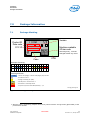
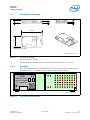
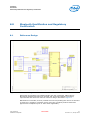
eUniStone BlueMoon™ Universal Platform Embedded PBA 31309 Intel Public User’s Manual Hardware Description Revision 1.2, 23-Sep-2013 Information in this document related to the Intel product or, if any, related to its use is provided in connection with Intel products. no license, express or implied, by estoppel or otherwise, to any intellectual property rights is granted by this document. except as provided in agreements concluded individually or Intel’s terms and conditions of sale for such products, Intel assumes no liability whatsoever and Intel disclaims any express or implied warranty, relating to sale and/or use of Intel products including liability or warranties relating to fitness for a particular purpose, merchantability, or infringement of any patent, copyright or other intellectual property right. legal lines and disclaimers Unless otherwise agreed in writing by Intel, the Intel products are not designed nor intended for any application in which the failure of the Intel product could create a situation where personal injury or death may occur. Unless otherwise agreed upon, Intel may make changes to specifications and product descriptions at any time, without notice. Designers must not rely on the absence or characteristics of any features or instructions marked “reserved” or “undefined”. Intel reserves these for future definition and shall have no responsibility whatsoever for conflicts or incompatibilities arising from future changes to them. Unless otherwise agreed, the information here is subject to change without notice. Do not finalize a design with this information. Contact your local Intel sales office or your distributor to obtain the latest specifications and before placing your product order. Copies of documents which have an order number and are referenced in this document, or other Intel literature, may be obtained by calling 1-800-5484725, or go to: http://www.intel.com/#/en_US_01. Any software source code reprinted in this document is furnished under a software license and may only be used or copied in accordance with the terms of that license. This document may contain information on products in the design phase of development. Intel product numbers are not a measure of performance. Product numbers differentiate features within each product family, not across different product families. Code Names are only for use by Intel to identify products, platforms, programs, services, etc. (“products”) in development by Intel that have not been made commercially available to the public, i.e., announced, launched or shipped. They are never to be used as “commercial” names for products. Also, they are not intended to function as trademarks. SMARTI, SMARTi & Device, BlueMoon, Comneon, Comneon & Device, M-GOLD, S-GOLD, E-GOLD, A-GOLD, X-GOLD, XMM, X-PMU, XPOSYS are trademarks of Intel Corporation and related companies. Copyright © 2013, Intel Corporation. All rights reserved. *Other names and brands may be claimed as the property of others. User’s Manual Hardware Description Intel Public The template (FrameMaker) of this document has been formally released by DOC department ([email protected]). Template data: T_TechDoc.fm, Rev. 2.00, 2012-04-01. 2 Revision 1.2, 23-Sep-2013 eUniStone PBA 31309 Revision History Page or Item Subjects (major changes since previous revision) Revision 1.2, 23-Sep-2013 <Revision X.Y>, <yyyy-mm-dd> User’s Manual Hardware Description Intel Public 3 Revision 1.2, 23-Sep-2013 eUniStone PBA 31309 Contents 1.0 General Device Overview........................................................................................... 8 1.1 Features ............................................................................................................ 8 1.2 Block Diagram .................................................................................................... 9 1.3 Pin Configuration LGA ........................................................................................ 10 1.4 Pin Description ................................................................................................. 11 1.5 System Integration ........................................................................................... 13 1.6 SW Patch in EEPROM ......................................................................................... 14 2.0 Basic 2.1 2.2 2.3 3.0 eUniStone Interfaces............................................................................................... 16 3.1 UART Interface ................................................................................................. 16 3.1.1 UART.................................................................................................... 16 3.1.1.1 Baud Rates .............................................................................. 16 3.1.1.2 Detailed UART Behavior............................................................. 17 3.1.1.3 UARTCTS Response Time ........................................................... 18 3.2 Low Power Control ............................................................................................ 18 4.0 General Device Capabilities ..................................................................................... 19 4.1 RF Test Application............................................................................................ 19 4.2 Firmware ROM Patching ..................................................................................... 19 4.2.1 Patch Support........................................................................................ 19 5.0 Bluetooth Capabilities ............................................................................................. 20 5.1 Supported Features ........................................................................................... 20 5.2 eUniStone Bluetooth Features ............................................................................. 20 5.2.1 Secure Simple Pairing ............................................................................. 20 5.2.2 Role Switch ........................................................................................... 20 5.2.3 Sniff Mode ............................................................................................ 21 5.2.4 Sniff Subrating ...................................................................................... 21 5.2.5 Enhanced Power Control ......................................................................... 21 5.2.6 Encryption Pause and Resume ................................................................. 21 6.0 Electrical Characteristics ......................................................................................... 22 6.1 Absolute Maximum Ratings................................................................................. 22 6.2 Operating Conditions ......................................................................................... 22 6.3 DC Characteristics............................................................................................. 23 6.3.1 Pad Driver and Input Stages .................................................................... 23 6.3.2 Pull-ups and Pull-downs .......................................................................... 25 6.3.3 Protection Circuits .................................................................................. 25 6.3.4 System Power Consumption .................................................................... 26 6.4 RF Part ............................................................................................................ 26 6.4.1 Characteristics RF Part............................................................................ 26 6.4.1.1 Bluetooth Related Specifications ................................................. 26 7.0 Package Information ............................................................................................... 29 7.1 Package Marking ............................................................................................... 29 7.2 Production Package ........................................................................................... 30 7.2.1 Pin Mark ............................................................................................... 30 Operating Information ................................................................................... 15 Power Supply ................................................................................................... 15 Clocking........................................................................................................... 15 Low Power Modes.............................................................................................. 15 2.3.1 Low Power Mode .................................................................................... 15 2.3.2 Complete Power Down ............................................................................ 15 2.3.3 ON/OFF ................................................................................................ 15 User’s Manual Hardware Description Intel Public 4 Revision 1.2, 23-Sep-2013 eUniStone PBA 31309 8.0 Bluetooth Qualification and Regulatory Certification ............................................... 31 8.1 Reference Design .............................................................................................. 31 8.2 FCC Class B Digital Devices Regulatory Notice....................................................... 32 8.3 FCC Wireless Notice........................................................................................... 32 8.4 FCC Interference Statement ............................................................................... 33 8.5 FCC Identifier ................................................................................................... 33 8.6 European R&TTE Declaration of Conformity........................................................... 34 8.7 Bluetooth Qualified Design ID ............................................................................. 34 8.8 Label Design of the Host Product......................................................................... 34 8.9 Regulatory Test House ....................................................................................... 34 8.10 Declaration of Conformity to European Standards .................................................. 35 9.0 Assembly Guidelines ............................................................................................... 36 9.1 General Description of the Module ....................................................................... 36 9.2 Printed Circuit Board Design ............................................................................... 37 9.3 Solder Paste Printing ......................................................................................... 38 9.4 Assembly ......................................................................................................... 38 9.4.1 Component Placement ............................................................................ 38 9.4.2 Pin Mark ............................................................................................... 38 9.4.3 Package................................................................................................ 39 9.5 Soldering Profile................................................................................................ 40 9.6 Rework ........................................................................................................... 41 9.6.1 Removal Procedure ............................................................................... 41 9.6.2 Replacement Procedure .......................................................................... 41 9.6.2.1 Alternative 1: Dispensing Solder ................................................. 41 9.6.2.2 Alternative 2: Printing Solder ..................................................... 42 9.7 Inspection........................................................................................................ 42 9.8 Component Salvage .......................................................................................... 43 9.9 Voids in the Solder Joints ................................................................................... 43 9.9.1 Expected Void Content and Reliability ....................................................... 43 9.9.2 Parameters with an Impact on Voiding ...................................................... 44 User’s Manual Hardware Description Intel Public 5 Revision 1.2, 23-Sep-2013 eUniStone PBA 31309 Figures 1 2 3 4 5 6 7 8 9 10 11 12 13 14 15 16 17 18 19 20 Simplified Block Diagram of eUniStone ......................................................................... 9 Pin Configuration for eUniStone in Top View (footprint) ................................................. 10 System Architecture Example with eUniStone .............................................................. 13 UART Interface ........................................................................................................ 16 UARTCTS Response Time .......................................................................................... 18 Package Marking ..................................................................................................... 29 Production Package .................................................................................................. 30 Top View and Bottom View........................................................................................ 30 Reference Design Schematics .................................................................................... 31 Cutout Drawing ....................................................................................................... 33 Equipment Label ...................................................................................................... 34 Declaration of Conformity ......................................................................................... 35 Pad Layout on the Module (top view) .......................................................................... 36 Cutout Drawing ....................................................................................................... 37 Pin Marking............................................................................................................. 38 Tape on Reel ........................................................................................................... 39 Eutectic Lead-Solder Profile ....................................................................................... 40 Eutectic Leadfree-Solder Profile ................................................................................. 40 Solder Printing ........................................................................................................ 42 X-ray Picture Showing Voids Conforming to IPC-A-610D................................................ 43 User’s Manual Hardware Description Intel Public 6 Revision 1.2, 23-Sep-2013 eUniStone PBA 31309 Tables 1 2 3 4 5 6 7 8 9 10 11 12 13 14 15 16 Pin Description ....................................................................................................... 11 UART Baud Rates .................................................................................................... 17 Default (non-inverted) behavior of UART signals ......................................................... 17 Absolute Maximum Ratings ...................................................................................... 22 Operating Conditions ............................................................................................... 22 Internal1 (1.5 V) Supplied Pins ................................................................................. 23 Internal2 (2.5 V) Supplied Pins ................................................................................. 23 VDDUART Supplied Pins ........................................................................................... 24 VDD1 Supplied Pins ................................................................................................. 24 ONOFF PIN ............................................................................................................ 24 Pull-up and Pull-down Currents ................................................................................. 25 Max. Load at the Different Supply Voltages ................................................................ 26 BDR - Transmitter Part ............................................................................................ 26 BDR -Receiver Part ................................................................................................. 27 EDR - Transmitter Part ............................................................................................ 27 EDR -Receiver Part .................................................................................................. 28 User’s Manual Hardware Description Intel Public 7 Revision 1.2, 23-Sep-2013 eUniStone PBA 31309 General Device Overview 1.0 General Device Overview 1.1 Features General • Complete Bluetooth 2.1 + EDR solution • Implements a single point-to-point data link to other SPP capable Bluetooth devices • Ultra low power design in 0.13 µm CMOS • Temperature range from -40°C to +85°C • Integrates Processor, RAM and patchable ROM • On-module voltage regulators. External supply 2.9 - 4.1 V • On-module EEPROM with configuration data • On-module tuned reference clock • Module can enter low power mode in idle state and during sniff intervals Interfaces • AT command interface over UART with HW flow control • Default UART baudrate 115200 bit/s • Module configuration reprogrammable for 9600 bit/s up to 3.25 Mbit/s UART baudrate • JTAG for boundary scan in production test RF • Class 2 device up to +4 dBm • Receiver sensitivity typ. -86 dBm • Integrated antenna, balun and ISM band filter • Integrated LNA with excellent blocking and intermodulation performance • Digital demodulation for optimum sensitivity and co-/adjacent channel performance User’s Manual Hardware Description Intel Public 8 Revision 1.2, 23-Sep-2013 eUniStone PBA 31309 General Device Overview Bluetooth • Bluetooth V2.1 + EDR compliant • Secure Simple Pairing • Device A (initiating link) or Device B (accepting link) roles supported • Single point-to-point data link, role switch supported • Packet data mode and stream data mode supported • Sniff mode and Sniff Subrating • 5 trusted devices stored in EEPROM • SW version available to configure specific RF certification tests 1.2 Block Diagram eUniStone EEPROM VDD1 I2C VDD_UART UART PMB8754 BlueMoon UniCellular GPIO Vsupply Balun Filter Voltage Regulator Crystal 26 MHz eUnistone_ Block_ Diagram.vsd Figure 1. Simplified Block Diagram of eUniStone User’s Manual Hardware Description Intel Public 9 Revision 1.2, 23-Sep-2013 eUniStone PBA 31309 General Device Overview 1.3 Pin Configuration LGA F1 VSS F2 P1.2 TDI F3 P0.11 F4 LPMin P0.14 F5 UARTCTS E1 P0.12 SDA0 E2 P013 SCL0 E3 P1.3 TDO E4 LPMout P0.0 D1 P0.10 D2 P0.8 D3 P1.1 TCK C1 VREG C2 P0.9 B1 P1.7 B2 P1.8 A1 VSS A2 P1.6 F6 F7 F8 VDDUART UARTTXD UARTRTS F9 VSS E5 P0.1 E6 UARTRXD E7 (NC) E8 VSS E9 VSS D4 P0.3 D5 P0.2 D6 (NC) D7 VSS D8 VSS D9 (NC) C3 JTAG# C4 TRST# C5 VDD1 C6 (NC) C7 (NC) C8 VSS C9 VSS B3 P1.0 TMS B4 P1.4 RTCK B5 ONOFF B6 (NC) B7 (NC) B8 (NC) B9 P0.15 A3 A4 VSUPPLY A5 VSUPPLY A6 VSUPPLY A7 VSS A8 P1.5 A9 VSS RESET# F11 VSS F12 VSS Top View A11 VSS A12 VSS PBA 31309 _Pinout.vsd Figure 2. Pin Configuration for eUniStone in Top View (footprint) User’s Manual Hardware Description Intel Public 10 Revision 1.2, 23-Sep-2013 eUniStone PBA 31309 General Device Overview 1.4 Pin Description The non-shaded cells indicate pins that will be fixed for the product lifetime. Shaded cells indicate that the pin might be removed/changed in future variants. Pins not listed below shall not be connected. Table 1. Pin No. Pin Description Symbol Input / Output Supply Voltage During Reset After Reset Function A2 P1.6 I/O/OD Internal1 Z Z Port 1.6 A3 RESET# AI Internal1 Input Input Hardware Reset A8 P1.5 I/O/OD Internal1 Input Input Port 1.5 B1 P1.7 I/O/OD Internal1 PD/ Input PD/ Input Port 1.7 B2 P1.8 I/O/OD Internal1 PD PD Port 1.8 B3 P1.0 / TMS I/O/OD Internal2 PU1 PU1. Port 1.0 or JTAG interface B4 P1.4 / RTCK I/O/OD Internal2 Z Z Port 1.4 or JTAG interface B5 ONOFF I - - Turns off module completely B9 P0.15 I/O VDDUART PD H Port 0.15 C2 P0.9 I/O/OD Internal2 Z Z Port 0.9 C3 JTAG# I Internal2 PU PU Mode selection Port 1: 0: JTAG 1: Port C4 TRST# I Internal2 PD PD JTAG interface D1 P0.10 I/O/OD Internal2 Z Z Port 0.10 D2 P0.8 I/O/OD Internal2 PD PD Port 0.8 D3 P1.1 / TCK I/O/OD Internal2 PU1. PU1. Port 1.1 or JTAG interface D4 P0.3 I/O/OD VDD1 Conf. PD def. Conf. PD def. Port 0.3 D5 P0.2 I/O/OD VDD1 Z Z Port 0.2 E1 P0.12 / SDA0 I/O/OD Internal2 PU PU I2C data signal E2 P0.13 / SCL0 I/O/OD Internal2 PU PU I2C clock signal E3 P1.3 / TDO I/O/OD Internal2 Z Z Port 1.3 or JTAG interface E4 P0.0 LPMout I/O/OD VDD1 PD PD Port 0.0 LPM wakeup output E5 P0.1 I/O/OD VDD1 PD PD Port 0.1 E6 P0.5 / UARTRXD I/O/OD VDDUART Z Z Port 0.5 or UART receive data F2 P1.2 / TDI I/O/OD Internal2 PU1. PU1. Port 1.2 or JTAG interface F3 P0.11 I/O/OD Internal2 Z Z Port 0.11 F4 P0.14 LPMin I/O VDDUART Z Z Port 0.14 LPM wakup input F5 P0.7 / UARTCTS I/O/OD VDDUART Z Z Port 0.7 or UART CTS flow control F7 P0.4 / UARTTXD I/O/OD VDDUART PU PU Port 0.4 or UART transmit data F8 P0.6 / UARTRTS I/O/OD VDDUART PU PU Port 0.6 or UART RTS flow control A4, A5, A6 VSUPPLY SI - - Power supply C1 VREG SO - - Regulated Power supply F6 VDDUART SI - - UART interface Power supply C5 VDD1 SI - - Power supply User’s Manual Hardware Description Intel Public 11 Revision 1.2, 23-Sep-2013 eUniStone PBA 31309 General Device Overview Table 1. Pin No. Symbol A1, A7, A9, A11, A12, C8, C9, D7, D8, E8, E9, F1, F9, F11, F12 VSS B6, B7, B8, C6, C7, D6, D9, E7 NC 1. Pin Description (Continued) Input / Output - Supply Voltage - During Reset After Reset Function - - Ground - - No connection Fixed pull-up/pull-down if JTAG interface is selected, not affected by any chip reset. If JTAG interface is not selected the port is tristate. Descriptions of acronyms used in the pin list: Acronym Description I Input O Output OD Output with open drain capability Z Tristate PU Pull-up PD Pull-down A Analog (e.g. AI means analog input) S Supply (e.g. SO means supply output) User’s Manual Hardware Description Intel Public 12 Revision 1.2, 23-Sep-2013 eUniStone PBA 31309 General Device Overview 1.5 System Integration eUniStone is optimized for a low bill of material (BOM) and a small PCB size. Figure 3 shows a typical application example. HOST Buttons, Leds LPM UART RESET AT command interface GPIO SPP(Serial Port Profile ) Oscillator API RFCOMM EEPROM Configuration , SW patch I2 C BT Stack BT Baseband Voltage BT RF Regulator BALUN Antenna System_Architecture.vsd VSUPPLY Figure 3. System Architecture Example with eUniStone User’s Manual Hardware Description Intel Public 13 Revision 1.2, 23-Sep-2013 eUniStone PBA 31309 General Device Overview The UART interface is used for communication between the host and eUniStone. The lines UARTTXD and UARTRXD are used for commands, events and data. The lines UARTRTS and UARTCTS are used for hardware flow control. Low power mode control of eUniStone and the host can be implemented by using the pins P0.14 and P0.0. P0.14 is used by the host to allow eUniStone to enter low power mode and P0.0 is used by eUniStone to wake-up the host when attention is required. To save current in idle mode, the host could hardware reset the module using the RESET#. Power is supplied to a single VSUPPLY input from which internal regulators can generate all required voltages. The UART and the GPIO’s interfaces have separate supply voltages so that they can comply with host signaling. 1.6 SW Patch in EEPROM Bugfixes for the SW in ROM are downloaded from the EEPROM. Intel may include new bugfixes in EEPROM during product lifetime. User’s Manual Hardware Description Intel Public 14 Revision 1.2, 23-Sep-2013 eUniStone PBA 31309 Basic Operating Information 2.0 Basic Operating Information 2.1 Power Supply eUniStone is supplied from a single supply voltage VSUPPLY. This supply voltage must always be present. The Bluetooth chip is supplied from an internally generated 2.5 V supply voltage. This voltage can be accessed from the VREG pin. This voltage shall not be used for supplying other components in the host system but can be used for referencing the host interfaces. The GPIO’s and the UART interface are supplied with dedicated, independent, reference levels via the VDD1 and VDDUART pins. All other digital I/O pins are supplied internally by either 2.5 V (Internal2) or 1.5 V (Internal1). Section 1.4 provides a mapping between pins and supply voltages. The I/O power domains (VDD1 and VDDUART) are completely separated from the other power domains and can stay present also in low power modes. 2.2 Clocking eUniStone contains a crystal from which the internal 26 MHz system clock is generated. Also, the low power mode clock of 32.768 kHz is generated internally, which means that no external clock is needed. 2.3 Low Power Modes To minimize current consumption, eUniStone automatically switches between different low power modes. The major modes are described below. 2.3.1 Low Power Mode In Low Power Mode (LPM) most parts of eUniStone are powered down. This is done automatically in idle mode or if the link is in Sniff mode and the host allows LPM with the pin P0.14. 2.3.2 Complete Power Down If Bluetooth functionality is not needed at all, VSUPPLY should be grounded to minimize power consumption. In this state there is no activity in eUniStone and the Bluetooth state (native clock, etc.) is not updated. 2.3.3 ON/OFF If VSUPPLY, VDDUART and VDD1 are supplied by the same source, it is not possible to switch off the module with the ONOFF pin. ONOFF shall then be connected to VSUPPLY. For details on how to use ONOFF, see the Design Guideline [3]. An alternative to save current in idle mode is to let the host hardware reset the module using the RESET# pin. Having the module in reset will turn off most parts in the module and make the module use a minimum of current. User’s Manual Hardware Description Intel Public 15 Revision 1.2, 23-Sep-2013 eUniStone PBA 31309 eUniStone Interfaces 3.0 eUniStone Interfaces 3.1 UART Interface The UART interface is the main communication interface between the host and eUniStone. AT commands are described in detail in the AT Commands specification [1]. The interface consists of four UART signals and two LPM control signals as shown in Figure 4. Host UARTTXD UARTRXD UARTRTS UARTCTS UARTTXD UARTRXD UARTRTS UARTCTS WAKEUP_BT WAKEUP_HOST eUniStone P0.14 input P0.0 output eUnistone_UART_Interface.vsd Figure 4. UART Interface 3.1.1 UART The lines UARTTXD and UARTRXD are used for commands, responses and data. The lines UARTRTS and UARTCTS are used for hardware flow control. A separate supply voltage, VDDUART, defines the UART reference levels to fit any system requirements. 3.1.1.1 Baud Rates The UART baud rate can be configured with the BD_DATA parameter UART_Baudrate. The module is programmed for a default baudrate of 115200 baud. Reprogramming of the EEPROM configuration is possible by AT commands at manufacturing time of the end product. The baudrate written to EEPROM will be used each time eUniStone starts or, HW or SW reset is done. The host is also able to change the baudrate temporarily with an AT command. This baudrate is used by eUniStone until a HW or SW reset is done, when it will change back to the baudrate stored in the EEPROM. User’s Manual Hardware Description Intel Public 16 Revision 1.2, 23-Sep-2013 eUniStone PBA 31309 eUniStone Interfaces Table 2 shows the UART baudrates supported. Table 2. UART Baud Rates Standard Baud Rate Module Baud Rate Deviation in % 9600 9615 0.16 19200 19230 0.16 38400 38461 0.16 57600 57522 -0.14 115200 115044 -0.14 230400 230088 -0.14 460800 464285 0.76 921600 928571 0.76 1843200 1857142 0.76 3250000 3250000 0 3.1.1.2 Detailed UART Behavior After reset the UART interface is configured with one start bit, eight data bits, no parity bit and one stop bit. The least significant bit is transmitted first. The polarity of the UART signals can be changed with the BD_DATA parameter UART_Invert. The default (non-inverted) behavior is shown in Table 3 Table 3. Default (non-inverted) behavior of UART signals Signal Level Meaning UARTTXD / UARTRXD 0 Start bit, ’0’ bit in character. 1 Idle level, stop bit UARTRTS / UARTCTS User’s Manual Hardware Description 0 Flow on 1 Flow stopped Intel Public 17 Revision 1.2, 23-Sep-2013 eUniStone PBA 31309 eUniStone Interfaces 3.1.1.3 UARTCTS Response Time Figure 5 shows the UARTCTS response time. Assuming non-inverted UART signals, the data flow stops within the “flow off response time” after UARTCTS has been set to high. If UARTCTS goes high during the transmission of a byte (phase 1 in the figure) this byte will be completely transmitted. While UARTCTS is high, no data will be transmitted (phase 2). When UARTCTS goes low again, data transmission will continue (phase 3). The maximum flow off response time is 10 UART bits (including start and stop bits). As an example, if the UART baud rate is 115200 Baud, the maximum flow off response time is 10 x 1/115200 s = 87 µs. max. flow off response time UARTCTS bit0 start stop bit7 bit6 bit5 bit4 bit3 bit2 bit1 bit0 UARTTXD start flow off response time ... phase 1 phase 2 phase 3 HCI_UARTCTS_Response_Time.vsd Figure 5. UARTCTS Response Time 3.2 Low Power Control Pin P0.14 and P0.0 are optional, but strongly recommended to be used. P0.14 is used to allow eUniStone to enter Low Power Mode (LPM). P0.0 is used by eUniStone when in LPM to wake up the host. User’s Manual Hardware Description Intel Public 18 Revision 1.2, 23-Sep-2013 eUniStone PBA 31309 General Device Capabilities 4.0 General Device Capabilities This chapter describes features available in the eUniStone (PBA 31309). Actual feature set and how to access the features can be found in the AT Command document [1]. Release specific performance characteristics, data throughput and current consumption are listed in the SW Release Notes [2]. 4.1 RF Test Application The eUniStone module can be programmed over UART with a specific application for RF test purposes, e.g. TX continuous or TX burst mode. This test application is controlled over the UART through Intel specific HCI commands. The commands supported by this test application are described in the document “T8753-2-Intel_Specific_HCI_Commands-7600.pdf”. 4.2 Firmware ROM Patching In any chip with complex firmware in ROM it is wise to support patching. The risk of project delay is significantly reduced when problems can be solved without hardware changes. Enhancements, adaptations and bug fixes can be handled very late during design-in, even after the chip has been soldered in the final product. The well-proven patch concept used in BlueMoon UniCellular is described below. 4.2.1 Patch Support The Bluetooth chip contains dedicated hardware that makes it possible to apply patches to the code and data in the firmware ROM. The hardware is capable of replacing up to 32 blocks of 16 bytes each with new content. This area can be filled with any combination of code and data. The firmware patch is stored in EEPROM and automatically loaded after startup. This provides a flexible bugfix solution for the software in ROM. User’s Manual Hardware Description Intel Public 19 Revision 1.2, 23-Sep-2013 eUniStone PBA 31309 Bluetooth Capabilities 5.0 Bluetooth Capabilities 5.1 Supported Features • Bluetooth V2.1 + EDR compliant • Enhanced Data Rate 2 and 3 Mbit/s symbol rate on the air • Secure Simple Pairing • Device A (initiating link) or Device B (accepting link) role supported • Single point-to-point data link, role switch supported • Packet data mode and stream data mode supported • Link in sniff mode supported. Device enters Low Power Mode in sniff intervals if permitted by the host. • Sniff Subrating • 5 trusted devices stored in EEPROM • Connection to a Bluetooth Tester 5.2 eUniStone Bluetooth Features 5.2.1 Secure Simple Pairing The device implements Secure Simple Pairing with the following association models according to Bluetooth V2.1 core specification: • Numeric Comparisoon • Just Works • Passkey Entry Also pairing with legacy (Bluetooth V2.0 and older) devices is supported. 5.2.2 Role Switch The initiating device (devA) starts as Bluetooth master of the link, the accepting device starts as Bluetooth slave of the link. The remote device can request a role change to accomodate with other Bluetooth links. If that happens, the module will send an event to the host. Also if the eUniStone start as slave, (Device B), the other device can change it's own role making eUniStone master. The host controlling eUniStone will be notified with the same event. User’s Manual Hardware Description Intel Public 20 Revision 1.2, 23-Sep-2013 eUniStone PBA 31309 Bluetooth Capabilities 5.2.3 Sniff Mode The local host or the remote device can request sniff mode for the link. During sniff mode, the devices synchronize on sniff instants only. The module will enter low power mode in the sniff intervals, if allowed by the host LPM control signals. Data packets can be exchanged at the sniff instants only, so the data rate is reduced in sniff mode. The module will wake up the host when data is received or other responses need to be transmitted. 5.2.4 Sniff Subrating The local host or the remote device can request Sniff Subrating for the link. When in sniff mode, the device will automatically switch between Sniff Mode and Sniff Subrating Mode making it possible to stay longer in Low Power Mode when there is no data transmitted or received. 5.2.5 Enhanced Power Control eUniStone support Enhanced Power Control according to Bluetooth specification 3.0. The Enhanced Power Control is handled automatically to make different modulations modes transmit on optimal levels. 5.2.6 Encryption Pause and Resume Encryption Pause Resume is supported making it possible to change connection link key on an encrypted link, pause the encryption and resume it with the new link key. This is handled automatically by eUniStone to make the link more secure. User’s Manual Hardware Description Intel Public 21 Revision 1.2, 23-Sep-2013 eUniStone PBA 31309 Electrical Characteristics 6.0 Electrical Characteristics 6.1 Absolute Maximum Ratings Table 4. Absolute Maximum Ratings Parameter Symbol Values Unit Note / Test Condition – Min. Typ. Max. Storage temperature -40 – 125 °C VSUPPLY supply voltage -0.3 – 6.0 V – VDDUART supply voltage -0.9 – 4.0 V – – VDD1 supply voltage -0.9 – 4.0 V VREG -0.3 – 4.0 V VSUPPLY > 4 V VREG -0.3 – VSUPPLY V VSUPPLY < 4 V ONOFF -0.3 – VSUPPLY+0.3 V Input voltage range -0.9 – 4.0 V Output voltage range -0.9 – 4.0 V -9 ESD – – 1.0 kV According to MIL-STD883D method 3015.7 – Note: Stresses above those listed here are likely to cause permanent damage to the device. Exposure to absolute maximum rating conditions for extended periods may affect device reliability. Maximum ratings are absolute ratings; exceeding only one of these values may cause irreversible damage to the integrated circuit. Maximum ratings are not operating conditions. 6.2 Operating Conditions Table 5. Operating Conditions Parameter Symbol Values Min. Typ. Unit Note / Test Condition Max. Operating temperature -40 – 85 °C – Main supply voltage (Vsupply) 2.9 – 4.11 V – VDDUART 1.35 – 3.6 V – VDD1 1.35 – 3.6 V – o 1. At ambient temperatures above 65 C the maximum allowed power dissipation in the module is limited to 200 mW User’s Manual Hardware Description Intel Public 22 Revision 1.2, 23-Sep-2013 eUniStone PBA 31309 Electrical Characteristics 6.3 DC Characteristics 6.3.1 Pad Driver and Input Stages For more information, see Chapter 1.4. Table 6. Internal1 (1.5 V) Supplied Pins Parameter Symbol Values Unit Note / Test Condition Min. Typ. Max. Input low voltage -0.3 – 0.27 V – Input high voltage 1.15 – 3.6 V – Output low voltage – – 0.25 V IOL = 1 mA Output high voltage 1.1 – – V IOH = -1 mA Continuous Load1 – – 1 mA – Pin Capacitance – – 10 pF – Magnitude Pin Leakage – 0.01 1 µA Input and output drivers disabled 1. The total continuous load for all Internal1 supplied pins shall not exceed 2 mA at the same time Table 7. Internal2 (2.5 V) Supplied Pins Parameter Symbol Values Unit Note / Test Condition Min. Typ. Max. Input low voltage -0.3 – 0.45 V – Input high voltage 1.93 – 2.8 V P0.10 Input high voltage 1.93 – 3.6 V Other pins Output low voltage – – 0.25 V IOL = 5 mA Output low voltage – – 0.15 V IOL = 2 mA Output high voltage 2.0 – – V IOH = -5 mA Output high voltage 2.1 – – V IOH = -2 mA Continuous Load1 – – 5 mA – Pin Capacitance – – 10 pF – Magnitude Pin Leakage – 0.01 1 µA Input and output drivers disabled 1. The total continuous load for all Internal2 supplied pins shall not exceed 35 mA at the same time User’s Manual Hardware Description Intel Public 23 Revision 1.2, 23-Sep-2013 eUniStone PBA 31309 Electrical Characteristics Table 8. VDDUART Supplied Pins Parameter Symbol Values Unit Note / Test Condition Min. Typ. Input low voltage -0.3 – Max. 0.2*VDDUART V – Input high voltage 0.7*VDDUART – VDDUART+0.3 V P0.5/UARTRXD Input high voltage 0.7*VDDUART – 3.6 V Other pins Output low voltage – – 0.25 V IOL = 5 mA VDDUART = 2.5 V Output low voltage – – 0.15 V IOL = 2 mA VDDUART = 2.5 V Output high voltage VDDUART -0.25 – – V IOH = -5 mA VDDUART = 2.5 V Output high voltage VDDUART -0.15 – – V IOH = -2 mA VDDUART = 2.5 V Continuous Load1 – – 5 mA – Pin Capacitance – – 10 pF – Magnitude Pin Leakage – 0.01 1 µA Input and output drivers disabled 1. The total continuous load for all VDDUART supplied pins shall not exceed 35 mA at the same time Table 9. VDD1 Supplied Pins Parameter Symbol Values Input low voltage Unit Note / Test Condition Min. Typ. Max. -0.3 – 0.2*VDD1 V – Input high voltage 0.7*VDD1 – 3.6 V – Output low voltage – – 0.25 V IOL = 5 mA VDD1 = 2.5 V Output low voltage – – 0.15 V IOL = 2 mA VDD1 = 2.5 V Output high voltage VDD1 -0.25 – – V IOH = -5 mA VDD1 = 2.5 V Output high voltage VDD1 -0.15 – – V IOH = -2 mA VDD1 = 2.5 V Continuous Load1 – – 5 mA – Pin Capacitance – – 10 pF – Magnitude Pin Leakage – 0.01 1 µA Input and output drivers disabled 1. The total continuous load for all VDD1 supplied pins shall not exceed 35 mA at the same time Table 10. ONOFF PIN Parameter Symbol Values Unit Note / Test Condition – Min. Typ. Max. Input low voltage – – 0.7 V Input high voltage 1.7 – VSUPPLY V – Input current -1 0.01 1 µA ONOFF = 0 V User’s Manual Hardware Description Intel Public 24 Revision 1.2, 23-Sep-2013 eUniStone PBA 31309 Electrical Characteristics 6.3.2 Pull-ups and Pull-downs Table 11. Pull-up and Pull-down Currents Pin Pull Up Current Pull Down Current Unit Conditions Pull-up current measured with pin voltage = 0 V Min. Typ. Max. Min. Typ. Max. P0.12 P0.13 260 740 1300 N/A N/A N/A µA P0.0 P0.1 P0.2 P0.3 22 130 350 23 150 380 µA P0.4 P0.5 P0.6 P0.7 P0.10 P0.8 P0.9 P0.11 P0.14 P0.15 4.2 24 68 3.0 20 55 µA P1.0 P1.1 P1.2 P1.3 P1.4 P1.5 P1.6 P1.7 P1.8 1.1 6.3.3 Pull-down current measured with pin voltage = supply voltage Min measured at 125°C with supply = 1.35 V Typ. measured at 27°C with supply = 2.5V Max measured at -40°C with supply = 3.63 V 6.0 17 0.75 5.0 14 µA Protection Circuits All pins have an inverse protection diode against VSS. P0.10 has an inverse diode against Internal2. P0.5/UARTRXD has an inverse diode against VDDUART. All other pins have no diode against their supply. User’s Manual Hardware Description Intel Public 25 Revision 1.2, 23-Sep-2013 eUniStone PBA 31309 Electrical Characteristics 6.3.4 System Power Consumption Table 12. Max. Load at the Different Supply Voltages Parameter Symbol Vsupply Values Min. Typ. Max. – – 100 Unit Note / Test Condition mA Peak current Note: I/O currents are not included since they depend mainly on external loads. For more details see [2]. 6.4 RF Part 6.4.1 Characteristics RF Part The characteristics involve the spread of values to be within the specific temperature range. Typical characteristics are the median of the production. All values refers to Intel reference design. 6.4.1.1 Bluetooth Related Specifications Table 13. BDR - Transmitter Part Parameter Symbol Values Unit Note / Test Condition Default settings Min. Typ. Max. Output power (high gain) 0.5 2.5 4.5 dBm Output power (highest gain) – 4.5 – dBm Maximum settings Power control step size 4 6 8 dB – – Frequency range fL 2400 2401.3 – MHz Frequency range fH – 2480.7 2483.5 MHz – 20 dB bandwidth – 0.930 1 MHz – 2nd adjacent channel power – -40 -20 dBm – 3rd adjacent channel power – -60 -40 dBm – >3rd adjacent channel power – -64 -40 dBm Max. 2 of 3 exceptions @ 52 MHz offset might be used Average modulation deviation for 00001111 sequence 140 156 175 kHz – Minimum modulation deviation for 01010101 sequence 115 145 – kHz – Ratio Deviation 01010101 / Deviation 00001111 0.8 1 – Initial carrier frequency tolerance |foffset| – – 75 kHz – Carrier frequency drift (one slot) |fdrift| – 10 25 kHz – Carrier frequency drift (three slots) |fdrift| – 10 40 kHz – Carrier frequency drift (five slots) |fdrift| – 10 40 kHz – Carrier frequency driftrate (one slot) |fdriftrate| – 5 20 kHz/50 ms – User’s Manual Hardware Description Intel Public – 26 Revision 1.2, 23-Sep-2013 eUniStone PBA 31309 Electrical Characteristics Table 13. BDR - Transmitter Part (Continued) Parameter Symbol Values Unit Note / Test Condition Min. Typ. Max. Carrier frequency driftrate (three slots) |fdriftrate| – 5 20 kHz/50 ms – Carrier frequency driftrate (five slots) |fdriftrate| – 5 20 kHz/50 ms – Table 14. BDR -Receiver Part Parameter Symbol Values Unit Note / Test Condition Min. Typ. Max. Sensitivity – -86 -81 dBm Ideal wanted signal C/I-performance: -4th adjacent channel – -51 -40 dB – C/I-performance: -3rd adjacent channel (1st adj. of image) – -46 -20 dB – C/I-performance: -2nd adjacent channel (image) – -35 -9 dB – C/I-performance: -1st adjacent channel – -4 0 dB – C/I-performance: co. channel – 9 11 dB – C/I-performance: +1st adjacent channel – -4 0 dB – C/I-performance: +2nd adjacent channel – -40 -30 dB – C/I-performance: +3rd adjacent channel – -50 -40 dB – Blocking performance 30 MHz - 2 GHz 10 – – dBm Some spurious responses, but according to BT-specification Blocking performance 2 GHz - 2.4 GHz -27 – – dBm – Blocking performance 2.5 GHz - 3 GHz -27 – – dBm – Blocking performance 3 GHz - 12.75 GHz 10 – – dBm Some spurious responses, but according to BT-specification Intermodulation performance -39 -34 – dBm Valid for all intermodulation tests Maximum input level -20 – – dBm – Table 15. EDR - Transmitter Part Parameter Symbol Values Min. Typ. Unit Note / Test Condition Max. Output power (high gain) -2.5 – 2 dBm Relative transmit power: PxPSK - PGFSK -4 -0.6 1 dB Carrier frequency stability |ωi| – – 75 kHz Carrier frequency stability |ωi+ω0| – – 75 kHz – – Carrier frequency stability |ω0| – 2 10 kHz – DPSK - RMS DEVM – 10 20 % – 8DPSK - RMS DEVM – 10 13 % – DPSK - Peak DEVM – 20 35 % – 8DPSK - Peak DEVM – 20 25 % – DPSK - 99% DEVM – – 30 % – 8DPSK - 99% DEVM – – 20 % – Differential phase encoding 99 100 – % – User’s Manual Hardware Description Intel Public 27 Revision 1.2, 23-Sep-2013 eUniStone PBA 31309 Electrical Characteristics Table 15. EDR - Transmitter Part (Continued) Parameter Symbol Values Unit Note / Test Condition Min. Typ. Max. 1st adjacent channel power – -40 -26 dBc – 2nd adjacent channel power – – -20 dBm Carrier power measured at basic rate 3rd adjacent channel power – – -40 dBm Carrier power measured at basic rate Table 16. EDR -Receiver Part Parameter Symbol Values Unit Note / Test Condition Min. Typ. Max. DQPSK-Sensitivity – -88 -83 dBm Ideal wanted signal 8DPSK-Sensitivityl – -83 -77 dBm Ideal wanted signal DQPSK - BER Floor Sensitivity – -84 -60 dBm – 8DPSK - BER Floor Sensitivity – -79 -60 dBm – DQPSK - C/I-performance: -4th adjacent channel – -53 -40 dB – DQPSK - C/I-performance: -3rd adjacent channel (1st adj. of image) – -47 -20 dB – DQPSK - C/I-performance: -2nd adjacent channel (image) – -31 -7 dB – DQPSK - C/I-performance: -1st adjacent channel – -7 0 dB – DQPSK - C/I-performance: co. channel – 11 13 dB – DQPSK - C/I-performance: +1st adjacent channel – -9 0 dB – DQPSK - C/I-performance: +2nd adjacent channel – -44 -30 dB – DQPSK - C/I-performance: +3rd adjacent channel – -50 -40 dB – 8DPSK - C/I-performance: -4th adjacent channel – -48 -33 dB – 8DPSK - C/I-performance: -3rd adjacent channel (1st adj. of image) – -44 -13 dB – 8DPSK - C/I-performance: -2nd adjacent channel (image) – -25 0 dB – 8DPSK - C/I-performance: -1st adjacent channel – -5 5 dB – 8DPSK - C/I-performance: co. channel – 17 21 dB – 8DPSK - C/I-performance: +1st adjacent channel – -5 5 dB – 8DPSK - C/I-performance: +2nd adjacent channel – -36 -25 dB – 8DPSK - C/I-performance: +3rd adjacent channel – -46 -33 dB – Maximum input level -20 – – dBm – User’s Manual Hardware Description Intel Public 28 Revision 1.2, 23-Sep-2013 eUniStone PBA 31309 Package Information 7.0 Package Information 7.1 Package Marking Product ID Date code FCC ID Version i intel PBA31309 V1.00 GYYWW /D FYWW9EXX FCC: PD9PBA31309 Machine readable 2D bar code Intel usage only , could be changed without any notice PCB Case Example of marking P B A 3 1 3 0 9 V 1 . 0 0 G Y Y W W / D F Y W W 9 E X X F C C I D : Q 2 3 3 1 3 0 8 Marking definition YYWW - calendar Year (2digits) + calendar week (2digits) of production F - lot code starts with F Y - last digit of assembly year (201 3) WW - assembly week = calendar week + 1 9E - final test ID + assembly site ID XX - unique lot sequential number 00-09,0A-0Z,10, …, ZZ Package_ Marking.vsd Figure 6. Package Marking 1 1. Warning: Early engineering samples have been printed with the wrong FCCID (Q2331308) of the predecessor module. User’s Manual Hardware Description Intel Public 29 Revision 1.2, 23-Sep-2013 eUniStone PBA 31309 Package Information 0,60 1,56 Production Package 1,80 7.2 8,70 15,60 Tolerances: +-0.2mm 121011 _ PAN1322 _V 1.0 .vsd Figure 7. Production Package All dimensions are in mm. Tolerances on all outer dimensions, height, width and length, are +/- 0.2 mm. 7.2.1 Pin Mark Pin 1 (A1) is marked on bottom footprint and on the top of the shield on the module according to Figure 8. Diameter of pin 1 mark on the shield is 0.40 mm. i intel F12 F11 PBA31309 V1.00 GYYWW /D FYWW9EXX FCC: PD9PBA31309 A12 Pin 1 marking top side A11 F9 F8 F7 F6 F5 F4 F3 F2 F1 E9 E8 E7 E6 E5 E4 E3 E2 E1 D9 D8 D7 D6 D5 D4 D3 D2 D1 C9 C8 C7 C6 C5 C4 C3 C2 C1 B9 B8 B7 B6 B5 B4 B3 B2 B1 A9 A8 A7 A6 A5 A4 A3 A2 A1 Pin 1 marking bottom side Top_and _Bottom_ Views.vsd Figure 8. Top View and Bottom View User’s Manual Hardware Description Intel Public 30 Revision 1.2, 23-Sep-2013 eUniStone PBA 31309 Bluetooth Qualification and Regulatory Certification 8.0 Bluetooth Qualification and Regulatory Certification 8.1 Reference Design Figure 9. Reference Design Schematics PBA 31309 is intended to be installed inside end user equipment. PBA 31309 is Bluetoooth-qualified and also FCC-certified and conforms to R&TTE (European) requirements and directives with the reference design described in Figure 9. Manufacturers of mobile, fixed or portable devices incorporating this device are advised to clarify any regulatory questions and to have their complete product tested and approved for compliance (FCC or other when applicable). User’s Manual Hardware Description Intel Public 31 Revision 1.2, 23-Sep-2013 eUniStone PBA 31309 Bluetooth Qualification and Regulatory Certification There are no parts in PBA 31309 that can be modified by the user except modifications of the device BD data and loading of SW patches. Any changes or modifications made to this device that are not expressly approved by Intel, may void the user’s authority to operate the equipment. 8.2 FCC Class B Digital Devices Regulatory Notice This equipment has been tested and found to comply with the limits for a Class B digital device, pursuant to Part 15 of the FCC Rules. These limits are designed to provide reasonable protection against harmful interference in a residential installation. This equipment generates, uses, and can radiate radio frequency energy and, if not installed and used in accordance with the instructions, may cause harmful interference to radio communications. However, there is no guarantee that interference will not occur in a particular installation. If this equipment does cause harmful interference to radio or television reception, which can be determined by turning the equipment off and on, the user is encouraged to try to correct the interference by 1 or more of the following measures: • Reorient or relocate the antenna • Increase the separation between the equipment and receiver • Connect the equipment into an outlet on a circuit different from that to which the receiver is connected • Consult the dealer or an experienced radio or television technician for help 8.3 FCC Wireless Notice This product emits radio frequency energy, but the radiated output power of this device is far below the FCC radio frequency exposure limits. Nevertheless, the device should be used in such a manner that the potential for human contact with the antenna during normal operation is minimized. To meet the FCC's RF exposure rules and regulations: • The system antenna used for this transmitter must not be co-located or operating in conjunction with any other antenna or transmitter. • The on-board antenna used must not be altered. • Users and installers must be provided with antenna installation instructions and transmitter operating conditions for satisfying RF exposure compliance. See Figure 10. User’s Manual Hardware Description Intel Public 32 Revision 1.2, 23-Sep-2013 eUniStone PBA 31309 Bluetooth Qualification and Regulatory Certification If possible place PBA31309 in the center of the main PCB. 8.7 5.00 Min. 15mm Min. 40mm Top View 15.6 3.00 Restricted Area No copper in any layer Place PBA31309 at the edge of the main PCB. Min. 15mm Use a Ground plane in the area surrounding the PBA31309 module wherever possible. Dimensions are in mm. Visio-Source-PAN1322.vsd Figure 10. Cutout Drawing Manufacturers of mobile, fixed or portable devices incorporating this module are advised to clarify any regulatory questions and to have their complete product tested and approved for FCC compliance. 8.4 FCC Interference Statement This device complies with Part 15 of the FCC Rules. Operation is subject to the following two conditions: 1. This device may not cause harmful interference 2. This device must accept any interference received, including interference that may cause undesired operation. 8.5 FCC Identifier FCC ID: PD9PBA31309 1 1. Warning: Early engineering samples have been printed with the wrong FCCID (Q2331308) of the predecessor module. User’s Manual Hardware Description Intel Public 33 Revision 1.2, 23-Sep-2013 eUniStone PBA 31309 Bluetooth Qualification and Regulatory Certification 8.6 European R&TTE Declaration of Conformity Hereby, Intel declares that the Bluetooth module PBA 31309 is compliant to R&TTE Directive 1999/5/EC with the protection requirements for Safety, EMC and RF Spectrum as specified in the following standards: EN 60950-1:2006+A11:2009+A12:2011+A1:2010+AC:2011; EN 62311:2008; EN 301 489-1 v1.9.2; EN 301 489-17 v2.2.1; EN 300 328 v1.8.1. As a result of the conformity assessment procedure described in Annex III of the Directive 1999/5/EC, the end-customer equipment should be labelled as follows: Figure 11. Equipment Label eUniStone in the specified reference design can be used in the following countries: Austria, Belgium, Bosnia-Herzegovina, Bulgaria, Croatia, Czech Rep, Cyprus, Denmark, Estonia, Finland, France, Germany, Greece, Hungary, Iceland, Ireland, Italy, Latvia, Liechtenstein, Lithuania, Luxemburg, Macedonia, Malta, Montenegro, Netherlands, Norway, Poland, Portugal, Romania, Slovakia, Slovenia, Spain, Sweden, Switzerland, UK 8.7 Bluetooth Qualified Design ID Intel has submitted an End Product Listings (EPL) for eUniStone PBA31309 in the Qualified Product List of the Bluetooth SIG. This EPL is referencing the Bluetooth qualification of the SPP-AT application running on the eBMU chip PMB8754 under QD ID B021246. Manufacturers of Bluetooth devices incorporating eUniStone or eBMU can reference the same QD ID number. Bluetooth QD ID: B021246 8.8 Label Design of the Host Product It is recommended to include the following information on the host product label: Contains transmitter Module FCC ID: PD9PBA31309. 8.9 Regulatory Test House The test house used by Intel in the Bluetooth and Regulatory approvals for the module PBA 31309: AT4wireless Parque Tecnologico de Andalucia c/ Severo Ochoa 2 E-29590 - Malaga SPAIN Tel: (34) 95 261 91 00 Fax: (34) 95 261 91 13 www.at4wireless.com TÜV Rheinland Nederland Eiberkamp 10 9351 VT Leek The Netherlands Phone +31 (0)594 505005 Fax +31 (0)594 504804 User’s Manual Hardware Description Intel Public 34 Revision 1.2, 23-Sep-2013 eUniStone PBA 31309 Bluetooth Qualification and Regulatory Certification 8.10 Declaration of Conformity to European Standards Figure 12. Declaration of Conformity User’s Manual Hardware Description Intel Public 35 Revision 1.2, 23-Sep-2013 eUniStone PBA 31309 Assembly Guidelines 9.0 Assembly Guidelines The target of this chapter is to provide guidelines for customers to successfully introduce the eUniStone module in production. This includes general description, PCBdesign, solder printing process, assembly, soldering process, rework and inspection. 9.1 General Description of the Module eUniStone is a Land Grid Array (LGA 6x12) module made for surface mounting. The pad diameter is 0.6 mm and the pitch 1.2 mm. All solder joints on the module will reflow during soldering on the mother board. All components and shield will stay in place due to wetting force. Wave soldering is not possible. Surface treatment on the module pads is Nickel (5-8 µm)/Gold (0.04 - 0.10 µm). Figure 13 shows the pad layout on the module, seen from the component side. 15.6 mm 5.0 1.2 2.4 F2 F3 F4 F5 F6 F7 F8 F9 E1 E2 E3 E4 E5 E6 E7 E8 E9 D1 D2 D3 D4 D5 D6 D7 D8 D9 C1 C2 C3 C4 C5 C6 C7 C8 C9 B1 B2 B3 B4 B5 B6 B7 B8 B9 A1 A2 A3 A4 A5 A6 A7 A8 A9 F11 F12 A11 A12 1. 35 1.2 F1 8.70 mm 0.6 1.35 1.0 0.6 Figure 13. Pad Layout on the Module (top view) User’s Manual Hardware Description Intel Public 36 Revision 1.2, 23-Sep-2013 eUniStone PBA 31309 Assembly Guidelines 9.2 Printed Circuit Board Design The land pattern on the PCB shall be according to the land pattern on the module, which means that the diameter of the LGA pads on the PCB shall be 0.6 mm. It is recommended that each pad on the PCB shall be surrounded by a solder mask clearance of about 75 µm to avoid overlapping solder mask and pad. If possible place PBA31309 in the center of the main PCB. 8.7 5.00 Restricted Area No copper in any layer Min. 40mm Top View Place PBA31309 at the edge of the main PCB. Min. 15mm 15.6 3.00 Min. 15mm Use a Ground plane in the area surrounding the PBA31309 module wherever possible. Dimensions are in mm. Visio-Source-PAN1322.vsd Figure 14. Cutout Drawing In order to preserve the characteristics of the embedded antenna, a cutout must be respected under the antenna through all metal layers of the PCB, as shown in drawing Figure 14. Placing the module inside a metal housing or close to metal parts like fasteners, shielding cages, washers, etc. can significantly affect the antenna characteristics. User’s Manual Hardware Description Intel Public 37 Revision 1.2, 23-Sep-2013 eUniStone PBA 31309 Assembly Guidelines 9.3 Solder Paste Printing The solder paste deposited on the PCB by stencil printing has to be of eutectic or near eutectic tin leadfree / lead composition. A no-clean solder paste is preferred, since cleaning of the solder joints is difficult because of the small gap between the module and the PCB. Preferred thickness of the solder paste stencil is 100 - 127 µmm (4 - 5 mils). The apertures on the solder paste stencil shall be of the same size as the pads, 0.6 mm. 9.4 Assembly 9.4.1 Component Placement In order to assure a high yield, good placement on the PCB is necessary. As a rule of thumb the tolerable misplacement is 150 µmm. This means that the eUniStone module can be assembled with a variety of placement systems. It is recommended to use a vision system capable of package pad recognition and alignment that evaluates the pad locations on the package (in contrast to outline centring). This eliminates the pad to package edge tolerance. The recommendation is to pick and place the module with a nozzle in the centre of the shield. The nozzle diameter shall not be bigger than 4 mm. 9.4.2 Pin Mark Pin 1 (A1) is marked on bottom footprint and on the top of the shield on the module according to Figure 15. Diameter of pin 1 mark on the shield is 0.40 mm. i intel F12 F11 PBA31309 V1.00 GYYWW /D FYWW9EXX FCC: PD9PBA31309 A12 Pin 1 marking top side A11 F9 F8 F7 F6 F5 F4 F3 F2 F1 E9 E8 E7 E6 E5 E4 E3 E2 E1 D9 D8 D7 D6 D5 D4 D3 D2 D1 C9 C8 C7 C6 C5 C4 C3 C2 C1 B9 B8 B7 B6 B5 B4 B3 B2 B1 A9 A8 A7 A6 A5 A4 A3 A2 A1 Pin 1 marking bottom side Top_and _Bottom_ Views.vsd Figure 15. Pin Marking User’s Manual Hardware Description Intel Public 38 Revision 1.2, 23-Sep-2013 eUniStone PBA 31309 Assembly Guidelines 9.4.3 Package eUniStone is packed in tape on reel according to Figure 16. Figure 16. Tape on Reel User’s Manual Hardware Description Intel Public 39 Revision 1.2, 23-Sep-2013 eUniStone PBA 31309 Assembly Guidelines 9.5 Soldering Profile Generally all standard reflow soldering processes (vapour phase, convection, infrared) and typical temperature profiles used for surface mount devices are suitable for the eUniStone module. Wave soldering is not possible. Figure 17 and Figure 18 shows example of a suitable solder reflow profile. One for leaded and one for leadfree solder. Recommended temp. profile for reflow soldering 10 1s 30 +20/-10s 235°C max. Temp.[°C] 220 5°C 200°C 150 10°C 90 30s Time [s] Lead _S older _P rof ile .v s d Figure 17. Eutectic Lead-Solder Profile Recommended temp. profile for reflow soldering (J-STD-020C) Temp.[°C] 260°C 255°C 30 sec max 217°C 60 ~ 150 sec 200°C 150°C 60 ~ 120 sec @ 3’C/sec max 6’C/sec max 25°C 8 minutes max Time [s] LeadF ree _S o lder _ P rof ile . v s d Figure 18. Eutectic Leadfree-Solder Profile User’s Manual Hardware Description Intel Public 40 Revision 1.2, 23-Sep-2013 eUniStone PBA 31309 Assembly Guidelines At the reflow process each solder joint has to be exposed to temperatures above solder liquids for a sufficient time to get the optimum solder joint quality, whereas overheating the board with its components has to be avoided. Using infrared ovens without convection special care may be necessary to assure a sufficiently homogeneous temperature profile for all solder joints on the PCB (especially on large, complex boards with different thermal masses of the components). The most recommended types are therefore forced convection or vapour phase reflow. Nitrogen atmosphere can generally improve solder joint quality, but is normally not necessary. The reflow profiles and other reflow parameters are dependent on the used solder paste. The paste manufacturer provides a reflow profile recommendation for this product. Additionally it is important not to overheat the eUniStone module by a too large reflow peak temperature. eUniStone contain several plastic packages and is there by sensitive of the moisture content level at the time of board assembly. Overheating in combination with excessive moisture content could result in package delaminations or cracks (popcorn effect). The heating rate should not exceed 3°C/s and max sloping rate should not exceed 4°C/s. eUniStone shall be handled according to MSL3, which means a floor life of 168 h in 30°C/60% r.h. The eUniStone module can be soldered according to max. J-STD-020C curve, assuming that all other conditions are followed stated in Product Specification, Qualification Report and in Application Note. Restriction is that PBA 31309 can be soldered two times, since one time is already consumed when soldering devices on Module. 9.6 Rework 9.6.1 Removal Procedure 1. Heat the module with an appropriate heating nozzle according to the instruction of the equipment or on a hot plate (about 225°C dependent on the board). Hot plate can only be used if the board is single side assembled. The temperature of the module shall be 200-220°C. 2. Use grippers or a pair of tweezers to remove the module. The module has to be gripped on two opposite edges of the module (not on the shield). 3. Remove excess solder by using solder sucker, suction soldering irons or solder wick. 9.6.2 Replacement Procedure Replacement can be done in two ways, dependent of how the solder is applied. Solder can be applied either by dispensing on the mother board or by printing the solder paste directly on the module. 9.6.2.1 Alternative 1: Dispensing Solder A dispenser with controlled volume must be used to assure the same volume on every pad. The volume on each pad shall be about 0.04 mm3. 1. Dispense 0.04 mm3 on each LGA pad 2. Pick the module by a nozzle and place in the right position on the board 3. Reflow the solder. User’s Manual Hardware Description Intel Public 41 Revision 1.2, 23-Sep-2013 eUniStone PBA 31309 Assembly Guidelines 9.6.2.2 Alternative 2: Printing Solder To print solder on the module a fixture must be used. The purpose of the fixture is to get a flat surface and fix the stencil and module for printing. An example of how this fixture can be designed is shown in Figure 19. S older paste stencil T ooling pins C avity of the module Vacuum hol es Fixture B ottom S older _P rint ing . v s d Figure 19. Solder Printing 1. Assemble the fixture to the bottom 2. Place the module in the cavity with the LGA pads upwards 3. Place the solder paste stencil on the fixture and make sure it fits to the tooling pins and the module 4. Apply vacuum to fix the solder paste stencil 5. Apply solder paste on the stencil and print by using a blade 6. Turn everything (bottom, fixture and stencil) upside down. 7. Separate carefully the bottom from the fixture 8. Pick the module by a nozzle and place in the right position on the board 9. Reflow the solder. 9.7 Inspection Automatic inspection of the solder paste printing before assembly is highly recommended to ensure high yield and good long term reliability. User’s Manual Hardware Description Intel Public 42 Revision 1.2, 23-Sep-2013 eUniStone PBA 31309 Assembly Guidelines 9.8 Component Salvage If it is intended to send a defect eUniStone module back to the supplier for failure analysis, please note that during the removal of this component no further defects must be introduced to the device, because this may hinder the failure analysis at the supplier. This includes ESD precautions, not to apply high mechanical force for component removal, and to prevent excess moisture content in the package during salvage (risk of pop corning failures). Therefore if the maximum storage time out of the dry pack (see label on packing material) is exceeded after board assembly, the PCB has to be dried 24h at 125°C before soldering off the defect component, because otherwise too much moisture may have been accumulated. 9.9 Voids in the Solder Joints 9.9.1 Expected Void Content and Reliability The content of voids is larger on LGA modules than for modules with BGA or leads. At a LGA solder joint the outgassing flux has a longer way to the surface of the solder and it has a relatively small surface to the air. The void content of the eUniStone module conforms to IPC-A-610D (25% or less voiding area/area). Figure 20 shows an example of void-content at a module assembled at production site. Normally you can see the whole spectra of void content variation within the same lot and occasion of assembly. V oids _I P C _A _ 610D .v s d Figure 20. X-ray Picture Showing Voids Conforming to IPC-A-610D User’s Manual Hardware Description Intel Public 43 Revision 1.2, 23-Sep-2013 eUniStone PBA 31309 Assembly Guidelines 9.9.2 Parameters with an Impact on Voiding If the void content has to be reduced following parameters have an impact. Solderability on module and PCB Bad solderability is often connected to oxidation and has therefore a major impact on voiding. Flux will get entrapped on oxidized surfaces. In general, Ni/Au pads show fewer voids than HASL and OSP. Solder paste Higher activity of the flux will remove oxide rapidly and less flux will get entrapped. Voiding increases with increasing solder paste exposure time, since long exposure time will result in more oxidation and moisture pickup. Pad size A large soldering pad means that the outgassing flux has a longer way to the surface of the solder, and will thereby create more voids. Solder paste Smaller powder size and higher metal load means more metal surface to deoxidize and thereby more entrapped flux and voiding. Higher metal load does also mean higher viscosity and more difficult for outgassed flux to remove from the solder. Stencil thickness A thick solder paste stencil means more surface area to the air and thereby easier for the outgassing flux to leave the solder. Temperature soldering profile Too short preheat time means that the flux does not get enough time to react and flux get entrapped in the solder and create voids. Too long reflow time gives larger voids Too short reflow time gives a fraction of voids User’s Manual Hardware Description Intel Public 44 Revision 1.2, 23-Sep-2013 eUniStone PBA 31309 References [1] Intel AT Command Specification (eUniStone_1.00_UM_SD.pdf) [2] Release Notes for SPP AT application SW version 1.1 (eUniStone_1.00_SW_3.1_RN.pdf) [3] eUniStone PBA31309 v1.00 - Design Guide (eUniStone_V1.00_AN_DesignGuide_Rev1.1.pdf) User’s Manual Hardware Description Intel Public 45 Revision 1.2, 23-Sep-2013 eUniStone PBA 31309 Terminology A ACK Acknowledgement ACL Asynchronous Connection-oriented (logical transport) AFH Adaptive Frequency Hopping AHS Adaptive Hop Sequence ARQ Automatic Repeat reQuest B b bit/bits (e.g. kb/s) B Byte/Bytes (e.g. kB/s) BALUN BALanced UNbalanced BD_ADDR Bluetooth Device Address BER Bit Error Rate BMU BlueMoon Universal BOM Bill Of Material BT Bluetooth BW Bandwidth C CDCT Clock Drift Compensation Task CMOS Complementary Metal Oxide Semiconductor COD Class Of Device CODEC COder/DECoder CPU Central Processing Unit CQDDR Channel Quality Driven Data Rate CRC Cyclic Redundancy Check CTS Clear To Send (UART flow control signal) CVSD Continuous Variable Slope Delta (modulation) D DC Direct Current DDC Device Data Control DM Data Medium-Rate (packet type) DMA Direct Memory Access DH Data High-Rate (packet type) DPSK Differential Phase Shift Keying (modulation) DQPSK Differential Quaternary Phase Shift Keying (modulation) DSP Digital Signal Processor DUT Device Under Test E EDR Enhanced Data Rate EEPROM Electrically Erasable Programmable Read Only Memory eSCO Extended Synchronous Connection-Oriented (logical transport) EV Extended Voice (packet type) F FEC User’s Manual Hardware Description Forward Error Correction Intel Public 46 Revision 1.2, 23-Sep-2013 eUniStone PBA 31309 FHS Frequency Hop Synchronization (packet) FIFO First In First Out (buffer) FM Frequency Modulation FW Firmware G GFSK Gaussian Frequency Shift Keying (modulation) GPIO General Purpose Input/Output GSM Global System for Mobile communication H HCI Host Controller Interface HCI+ Intel Specific HCI command set HEC Header Error Check HV High quality Voice (packet type) HW Hardware I I2C Inter-IC Control (bus) I2S Inter-IC Sound (bus) IAC Inquiry Access Code ID IDentifier IEEE Institute of Electrical and Electronics Engineers IF Intermediate Frequency ISM Industrial Scientific & Medical (frequency band) J JTAG Joint Test Action Group L LAN Local Area Network LAP Lower Address Part LM Link Manager LMP Link Manager Protocol LNA Low Noise Amplifier LO Local Oscillator LPM Low Power Mode(s) LPO Low Power Oscillator LSB Least Significant Bit/Byte LT_ADDR Logical Transport Address M MSB Most Significant Bit/Byte MSRS Master-Slave Role Switch N NC No Connection NOP No OPeration NVM Non-Volatile Memory O OCF Opcode Command Field OGF Opcode Group Field P PA Power Amplifier PCB Printed Circuit Board PCM Pulse Coded Modulation PDU Protocol Data Unit PER Packet Error Rate PIN Personal Identification Number User’s Manual Hardware Description Intel Public 47 Revision 1.2, 23-Sep-2013 eUniStone PBA 31309 PLC Packet Loss Concealment PLL Phase Locked Loop PMU Power Management Unit POR Power-On Reset PTA Packet Traffic Arbitration PTT Packet Type Table Q QoS Quality Of Service R RAM Random Access Memory RF Radio Frequency ROM Read Only Memory RSSI Received Signal Strength Indication RTS Request To Send (UART flow control signal) RX Receive RXD Receive Data (UART signal) S SCO Synchronous Connection-Oriented (logical transport) SIG Special Interest Group (Bluetooth SIG) SW Software SYRI Synthesizer Reference Input T TBD To Be Determined TCK Test Clock (JTAG signal) TDI Test Data In (JTAG signal) TDO Test Data Out (JTAG signal) TL Transport Layer TMS Test Mode Select (JTAG signal) TX Transmit TXD Transmit Data (UART signal) U UART Universal Asynchronous Receiver & Transmitter ULPM Ultra Low Power Mode V VCO Voltage Controlled Oscillator W WLAN Wireless LAN (Local Area Network) User’s Manual Hardware Description Intel Public 48 Revision 1.2, 23-Sep-2013 This document has been formally released by DOC department ([email protected]) on October 4, 2013