1
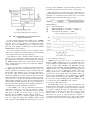
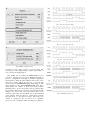
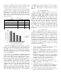
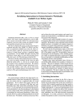
Enhanced LEON3 Low Power IP Core for DSM
Technologies
Krzysztof Marcinek, Arkadiusz W. Luczyk and Witold A. Pleskacz
Institute of Microelectronics and Optoelectronics
Warsaw University of Technology
ul. Koszykowa 75, 00-662 Warsaw, Poland
[email protected], [email protected], [email protected]
Abstract—Power consumption is one of the most important
factor in a modern embedded System-on-Chip's (SoC's) design.
Increasing computation complexity and incessant growth of clock
frequency reveals the necessity for dynamic and smart utilization
of the available hardware resources. The paper presents
Enhanced LEON3 Low Power IP Core with superscalar abilities
and Low Power Management Unit (LPMU). In comparison with
the original LEON3 IP core, the new one may execute up to two
instructions per cycle and dynamically manage incorporated
power domains. Enhanced LEON3LP IP core was synthesized
using TSMC 90 nm CMOS technology.
Index Terms—DSM, LEON3, power management, low-power,
superscalar, microprocessor
I.
INTRODUCTION
Power consumption in SoC Integrated Circuits (ICs) can
be divided into two categories. The first one is the dynamic
power consumption caused by performing useful operations
and it is proportional to the number of transistor state changes
per second. The second one is the static power consumption,
which is the result of the sub-threshold leakage current and it
is dissipated even if the device is not working. Although in the
past days static power could be ignored, in today’s deep
sub-micron (DSM) technologies it plays a significant role in
the total power consumption. Therefore, it is essential to
incorporate low-power techniques during the development of
modern SoC designs.
The easiest way to reduce dynamic power is to decrease
the clock frequency. However, clock frequency defines system
performance, so nowadays it cannot be taken under
consideration in many applications. Superscalar processing [1]
allows us to take the advantage of reducing clock frequency
without affecting the performance. A typical superscalar
processor performs more than one instruction during the same
clock cycle, which means faster program execution and minor
demands for operating frequency. Although more complex
computation means extended hardware resources, additional
Funcional Units (FU's) have less impact on the occupied area
and the power consumption then a multi-core approach.
Studies in superscalar processors [2] show that for
a significant amount of time particular FU's remain idle
consuming static power. Power gating [3] is one of the most
commonly used low-power technique in order to avoid this
power loss. While cutting of power supply of the unused FU,
source of all parasitic currents is removed.
Enhanced LEON3 Low Power IP Core extends
well-known open-source LEON3 IP core processor [4] with
superscalar abilities and power control feature. LEON3 is
available in form of a synthesizable VHDL model based on
SPARC V8 [5] instruction set architecture (ISA). The other
benefit of using LEON3 is the availability of the TSIM
simulator [6] and the BCC cross-compiler [7], which are
essential to perform a comparative analysis between the
original and the enhanced IP core.
The paper is organized as follows. The microarchitecture
of LEON3 processor IP core is briefly presented in Section II.
Section III describes Enhanced LEON3 Low Power IP core.
The paper ends with synthesis results and conclusion.
Fig. 1. LEON3 core block diagram
II.
LEON3 PROCESSOR MICROARCHITECTURE
LEON3 processor system allows the user to customize it
for certain application due to its configuration abilities. The
system is based on LEON3 core connected through AMBA bus
[8] to system peripherals. For the use of this work the core was
configured to incorporate separated data and instruction cache
controllers with AMBA bus interface, interrupt port and
hardware, divide and multiply unit (Fig. 1). The register file is
a 3-port memory with separated write port and two read ports.
It contains general purpose global registers and register
windows in number within the limit of the SPARC V8
standard. The integer unit (IU) datapath is based on a 7-stage
pipeline with Harvard architecture.
IU may perform arithmetic, logical and shift operations, and
its unnecessary parts are removed to reduce occupied area.
Data dependency is another issue that is handled in the
modified IU. The results from four pipeline stages (execute to
writeback) are exchanged between both IU's to feed their
arithmetic and logical unit (ALU) when necessary.
Field Definitions:
[31:3]
[2]
[1]
[0]
Fig. 2. Enhanced LEON3LP core block diagram
III.
: Unused. Read as 0.
: DIV Unit Enable. 0 – automatic, 1 – always on
: MUL Unit Enable. 0 – automatic, 1 – always on
: Secondary IU. 0 – disable, 1 – enable
Fig. 3. Power Management Register (%asr20)
ENHANCED LEON3 LOW POWER PROCESSOR
MICROARCHITECTURE
For the research, grlib-gpl-1.0.17-b2710 version of GRLIB
was used. To obtain execution of two instructions at the same
time and power control a number of modifications in the
original source code of LEON3 processor system were taken.
The new block diagram of Enhanced Low Power LEON3
(ELEON3LP) is shown in Fig. 2.
In order to handle the execution of two instructions at the
same time, the register file enables reading of four and writing
of two independent data words at the same time.
The instruction cache controller enables fetching of two
valid consecutive instructions. During cache miss however,
the instructions are fetched from an external memory through
the AMBA interface. In this case, only the Primary IU has the
data to handle and the Secondary IU executes the NOP (no
operation) instruction.
Superscalar Controller is a stand-alone entity that extends
the LEON3 pipeline with an additional Prefetch stage. It is
situated between the instruction cache controller and both
integer units. After fetching of two consecutive instructions,
the Prefetch stage decides whether the instructions can be
executed in parallel or one after another. In the first case, the
fetched instructions are directed to the appropriate integer unit.
In the other case, only the first instruction feeds Primary IU
(IU0) pipeline, while the Secondary IU (IU1) remains unused
and executing the NOP instruction. The second instruction is
fetched again in the following cycle. A detailed explenation of
extended pipeline functioning can be found in [9].
Source VHDL code of IU is parameterized and may be
either used as Primary IU or Secondary IU. However, only the
Primary IU is connected to the instruction cache controller,
data cache controller, and it has access to the processor
internal registers (SPARC V8 ISA registers: PSR, Y, ...).
Therefore, it is the only one, which is capable of performing
load, store, jump, call, branch, trap, multiply, divide, and all
other operations using SPARC V8 ISA registers. Secondary
Fig. 4. Power down/up signals order
A. Power Managment Register
SPARC V8 [5] provides for up to 31 Ancillary State
Registers (ASRs), numbered from 1 to 31. ASRs from 16 to
31 are available for implementation-dependent use and can be
read or written using RDASR and WRASR assembly
instructions [10]. Originally, LEON3 (ELEON3 as well) uses
ASRs from 24 to 31, to implement hardware breakpoints, and
ASR17 as a processor configuration register. Moreover,
writing a value of zero to ASR19 makes the processor to enter
“power-down” mode (which holds the pipeline). The Low
Power version of ELEON3 processor implements an ASR20
register named Power Management Register (PMR) (Fig. 3).
It is used by Low Power Management Unit (LPMU) in order
to control power state of ELEON3 power domains.
B. Low Power Management Unit
The LPMU (Fig. 2) can control up to four separate power
domains and its main task is to generate sequence of power
down and power up signals [11]. If power back up in a known
good state is required, then the save signal holds content of
internal registers. Otherwise, the first step to power down the
unused block is to isolate it from the remaining parts.
Afterwards, the power is removed and the sequence of
powering down is finished. The reverse order of these signals
are needed to generate power up sequence. Firstly, the power
Fig. 7. Primary IU power down/up
Fig. 5. Processor configuration menu
Fig. 8. Secondary IU power down
Fig. 9. Secondary IU power up
Fig. 6. LPMU configuration menu
is turned on and register content is restored. After that,
removing the isolate signal brings complete functionality of
once powered off module (Fig. 4).
The LPMU can be enabled in ELEON3LP processor
system by entering the 'Low-power Management Unit' in
processor configuration menu (Fig. 5). LPMU configuration
menu enables to define the pulse width in clock cycles of save
and restore signals, which are necessary to provide state
retention (TSR – SAVE/RESTORE pulse width in Fig. 4). The
other parameter is TIS (ISOLATE/SHUTOFF delay time),
which defines the number of clock cycle delay between
particular phases of power down and power up sequence (Fig.
6). As divide instructions are much more uncommon then the
multiply ones, due to their very long execution time, it was
decided to place DIV Unit and MUL Unit in the individual
power domains. Such step allows to control them separately
and turn them on only when necessary. The next power
domain is occupied by the Secondary IU to minimize
processor power consumption while executing non-optimized
Fig. 10. Automatic MUL/DIV power up/down
Fig. 11. MUL/DIV power down
and hard to parallelize programs. The forth LPMU output
interface is used to retain the state of Primary IU, Superscalar
Controller and Data and Instruction Cache Controllers.
When the processor enters power-down mode, the LPMU
starts the sequence of turning off the all controlled domains,
bringing the power consumption to the minimum. Due to the
state retention of the Primary IU, after being woken up by
LPMU because of incoming interrupt, the processor can
restore its state, handle the interrupt and continue executing
the program (Fig. 7).
TABLE I.
POWER ESTIMATION
Power Domains
Dynamic [mW]
Total [mW]
all on
31.412
31.480
IU1 off @(MUL–on; DIV–on; IU0–on)
26.692
26.748
MUL off @(IU1–off; DIV–on; IU0–on)
19.699
19.744
DIV off @(IU1–off; MUL–off; IU0-on)
17.233
17.273
all off
0.358
0.359
or ASR20[2] will hold these modules powered on the whole
time. After switching back to automatic mode, the MUL and
DIV Units will be turned off right after timer overflow
(Fig. 11).
IV. SYNTHESIS RESULTS
Mentor Graphics ModelSim software was used as
a simulation environment. ELEON3LP processor IP core was
synthesized in TSMC 90 nm CMOS technology using
Cadence RTL compiler. Table I shows the results of power
estimation of the ELEON3LP with a toggle rate – 0.2,
probability rate – 0.5 and 3 ns clock period. Processor
system’s power domains are successively turning off till the
complete shut down. The cache and register file memories
were not the subject of the synthesis, so their power
consumption was not included in the results. Fig. 12 shows
that additional Secondary IU has an insignificant impact on
the overall power consumption. Starting from 31.48 mW
power consumption of all-power-on system, the LPMU can
reduce it to 359 µW powering all the incorporated power
domains off.
V.
Fig. 12. Power estimation diagram
When the programmer does not intend to use the
Secondary IU, the ARS20[0] should be cleared. In this case
Superscalar Controller stops feeding it with new instructions
and LPMU powers it down after insuring that its pipeline is
empty (Fig. 8). The Superscalar Controller will use again the
Secondary IU right after it is turned on and restart after setting
bit 0 in the ASR20 (Fig. 9).
The value of zero in ASR20[1] or ASR20[2] means that
LPMU will automatically power up the DIV or MUL Unit
when necessary and power it down while unused for a specific
period of time. After detecting a multiplication or division
instruction in the pipeline, the appropriate signal indicates the
need of turning it on and the timer is started. The processor
execution pipeline is being held for the time of complete
powering up of the MUL or DIV Unit delaying their start
conditions. This is the only time penalty and performance
degradation, because of using automatic LPMU mode. Each
multiply or divide instruction appearance resets the
appropriate timer. Once powered up, the MUL or DIV Unit
will be automatically turned off after not being used for 256
clock cycles (Fig. 10). Writing the value of one in ASR20[1]
CONCLUSION
Enhanced LEON3LP IP core with ability to execute two
instructions in parallel and Low Power Management Unit was
presented in the paper. The results of power estimation
showed that the additional Secondary IU (IU1) has an
insignificant impact of 4.72 mW in comparison with
31.48 mW power consumption of the whole processor core.
Existence of the LPMU allows the user to match the power
consumption to the requirements of the running software. By
using dynamic management of the power domains, the LPMU
can adjust the power consumption from 31.48 mW to
17.23 mW for the running processor and drop it to 359 µW
during the power-down state.
REFERENCES
[1]
James E. Smith, Gurindar S. Sohi, “The microarchitecture of superscalar
processors”, Proceedings of the IEEE, Volume 83, Issue 12,
pp. 1609 – 1624, Dec 1995.
[2] Zhigang Hu, A. Buyuktosunoglu, V. Srinivasan, V. Zyuban, H.
Jacobson, P. Bose, “Microarchitectural techniques for power gating of
execution units”, ISLPED 2004, Proceedings of the 2004 International
Symposium on Low Power Electronics and Design, Page(s): 32 – 37,
Aug. 2004.
[3] M. Powell, Se-Hyun Yang, B. Falsafi, K. Roy, T. N. Vijaykumar,
“Gated-Vdd: a circuit technique to reduce leakage in deep-submicron
cache memories”, ISLPED 2000, Proceedings of the 2000 International
Symposium on Low Power Electronics and Design, Page(s): 90 – 95.
[4] “GRLIB IP CORE User's Manual”, http://www.gaisler.com/.
[5] “The SPARC architecture manual Version 8”, http://www.sparc.org/.
[6] “TSIM2 Simulator User's Manual”, http://www.gaisler.com/.
[7] “BCC
Bare-C
Cross-Compiler
User's
Manual”,
http://www.gaisler.com/.
[8] “AMBA Specification (Rev. 2.0)”, http://www.arm.com/.
[9] K. Marcinek, A. W. Łuczyk, W. A. Pleskacz, “Enhanced LEON3 core
for superscalar processing”, DDECS '09, Design and Diagnostics of
Electronic Circuits and Systems, 2009, Page(s): 238 – 241, Apr. 2009.
[10] “SPARC assembly language reference manual”, http://docs.sun.com/.
[11] C. Komar, T. Anderson, J. Church, “Formal validation of low-power
designs”, Cadence Design System, http://www.cadence.com/.