1
DBM 03
User's Manual
GB-4019 Rev.9 - July/98
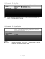
DBM 03 - USER'S MANUAL
Rev
.
0
1
2
3
4
5
6
7
8
9
Date
Description
June/95
Initial Release
22/June/95 Correct miscellaneous errors
6/July/95
Correct miscellaneous errors
28/Sept/95 Correct miscellaneous errors
24/Oct/95 Add facilities to change DBM01 with DBM03
6/May/96
Add reference to DBTALK program and
pinouts of RS232/RS485 converter; correct
OC, OV, VO commands; update personality
card; add DBM-PS internal card jumpers;
correct miscellaneous errors
30/July/96 Add EMC paragraph; update motor connector
pinout (Fig.1.13); correct soft start
configuration (Fig.2.1, 2.2); update resolver
wiring (Fig.2.3) according to EMC; correct
miscellaneous errors
6/Feb/97
Add Section 6 (EMC); change par.1.6 (CEmarking); update all wiring figures according
to EMC; add Appendix A (serial link
multidrop); add Appendix B (Dbtalk
communication program); update par.2.2.7
(personality card); correct miscellaneous
errors
23/May/97 Update standards with EN 61800-3, EMC
product standard; correct fig.6.8
(EMC/Equipotential bonding); update 220Vac
with 230Vac; correct tab.3.5 (IT/PC); correct
the leakage current of EMC filters; correct
miscellaneous errors
6/July/98
Add Appendix C, D and E; add default values
for keyboard setup; add reset to enable SE
command; correct miscellaneous errors
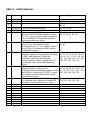
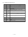
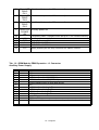
Updated Pages
52, 84, 111
7, 27, 28, 29, 33, 66, 68, 84,
86, 91
55, 73, 83, 94
52
7, 28, 33, 48, 49, 50, 51, 52,
63, 79, 80, 87, 90, 121
1, 3, 5, 8, 33, 35, 42, 44, 46,
61, 86
1, 2, 5, 6, 8, 13, 24, 27, 29,
30, 31, 34, 35, 38, 45, 46, 48,
49, 52, 56, 75, 82, 85, 88,
123, 124,125, 126, 127, 128,
129, 130, 131, 132, 133
3, 5, 6, 8, 9, 11, 25, 37, 42,
43, 44, 48, 49, 52, 56, 57, 72,
75, 98, 99, 101, 105, 123,
125, 128, 129, 132, 133
2, 43, 48, 55, 83, 85, 94, 123,
125, 130, 134, 135, 136
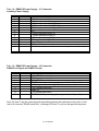
Table of Contents
Introduction
page
3
Section 1
Description
general features
standard features
technical data
interfaces
protections
CE marking
system wiring
configurations
internal jumpers
dimensions
fans
recovery circuit
block diagrams
5
5
6
7
7
8
8
8
13
36
37
37
39
Section 2
Installation
wiring
transformer/autotransformer connection
soft start
resolver wiring
motor power wiring
connection to PC
installation
keyboard or opto priority
autophasing
personality card jumpers
resolver to encoder (optional)
operation
43
43
45
47
47
48
48
49
49
52
53
57
Section 3
Commands and
Protections
general features
commands
protections
58
60
92
Section 4
Troubleshooting
Section 5
Principles of
Operation
98
introduction
torque generation
current control loop
speed and position sensing
speed loop
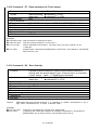
1 - 6/July/98
114
114
117
119
121
Section 6
EMC
European Directive
filtering
wiring and grounding
recovery resistor
screening
safety aspects
123
123
126
128
129
130
Appendix A
Multidrop
internal jumpers
personality card jumpers
131
131
Appendix B
Dbtalk
dbtalk communication program
132
Appendix C
module replacement
134
Appendix D
input sizing
135
Appendix E
mechanical brake
136
2 - 6/July/98
Introduction
This manual provides the necessary information for a proper installation and an effective use
of DBM Digital Drives in the possible different configurations.
Its contents allow technicians to understand how the system works and to carry out
installation procedures.
The safety instructions provided in this Manual are included to prevent injury to personnel
(WARNINGS) or damage to equipment (CAUTIONS).
To emphasize the differences between new DBM 03 User's Manual and old DBM 01 User's
Manual, a vertical line in the left margin of the text indicates new items.
Accident Protection
Keep to the general security rules for electrical equipment's. DBM-PS power supply is
electrically connected to mains.
WARNING: High Voltage. L+ and L- pins and BUS BAR can have voltage
≥300Vdc even after switching off (capacitive voltage). Discharge
Time Approx. 6 Minutes.
WARNING: High Voltage. The recovery resistor is connected to the Bus Bar’s
and can have voltage ≥300Vdc.
WARNING: do not touch recovery resistor during operation to avoid scalds.
WARNING: when required for an emergency stop, opening motor phases must
be preceded by disabling the axis. The delay time must be at least
30 ms.
WARNING: the drive should be located in an environment that is free from dust,
corroding fumes and fluids. In condensing atmospheres, the cabinet
must be provided with an anti-condensation device.
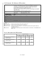
Tightening Torque
CAUTION: do not exceed the tightening torque of the table
Screw
Thread
M3
M4
M5
M6
M8
Tightening torque
[Nm]
[lb in]
1.00
8.85
3.00
26.55
6.00
53.10
8.00
70.80
20.0
177.0
3 - 6/July/98
4 - 6/July/98
SECTION 1 - DESCRIPTION
1.1 General Features
The modular DBM series drives offer digital speed loop and digital analog interfaces. They
are suitable for use with 4-quadrant, brushless motors having sinusoidal back e.m.f. .
Construction allows the use of the power amplifiers only, if required for easy CNC interface.
Hardware circuits are reduced by using Isolated Gate Bipolar Transistor (IGBT) components
in the power section.
Control technique is sinusoidal.
The unique advantages of the digital technology (16/32 bit DSP based) are:
•
•
•
•
Simplified installation through optimization of control parameters via software.
No potentiometer adjustments.
Autophasing.
Easy adaptation to different applications: e.g. you may change the PI gain variables and
choose between speed or torque control.
• Compact assembly: up to 3-axis control from a single module.
• Flexibility: up to 99 axes, 240A peak per axis.
1.2 Standard Features
•
•
•
•
•
•
•
•
•
•
•
•
•
•
•
•
Three-phase full bridge with IGBT
Current reference refresh time: 100 µs
Phases refresh time: 300 µs
R/D resolution automatically switched according to actual speed for optimum system
performance (between 10 and 16 bit)
Resolution of A/D converter: 12 bit or 14 bit (optional)
4 different velocity control structures to meet the most challenging requirements
Digital low-pass filter on speed loop
Over travel limit switches available (when Expansion is not present)
Totally programmable control and interface parameters
Current bandwidth (analog) > 1kHz
Dead point: absent
Speed ratio: 1:4000
Static current gain 10 5 A/V
Max operating temperature / humidity: 45 °C (113 °F) / 90%
Derating for altitude > 1000 m (3333 feet): 1% per 100 m (333 feet)
Storage temperature: -10 to +70 °C
5 - 6/July/98
1.3 Technical Data
DBM Module
Input voltage
Three-phase output voltage
: 300Vdc, ±10%
: 180V
DBM-PS Power Supply
Three-phase input voltage
Auxiliary power supply input voltage
Auxiliary input power
BUS BAR output voltage
: 230Vac, ±10%, 50/60 Hz
: 110Vac (optional) or 230Vac, ±10%, 50/60 Hz
: 55W for 3-axis module, 60W for fans pair
: 300Vdc
230
230
6 - 6/July/98
1.4 Interfaces
Digital
• Output for simulated encoder (optional)
• Serial Link RS485(1200-19200 Baud) full-duplex to manage:
- Acceleration limits
- Autophasing
- Control parameters
- Monitoring of internal parameters
- Range of analog interface
- System status
• Output for Drive OK axis 1, axis 2, axis 3 (TTL compatible)
On-Off (Optoisolated)
• Drive OK
• Drive Enable
• Motor OK
• Reference Enable
Analog
• Input velocity (see MR command)
• Resolver differential input signals
• Peak current limit input
• Output tachometer (see ET command)
• Max current, velocity reference, velocity error outputs (see ES, SO commands)
1.5 Protection
Module
• Auxiliary voltage out of tolerance
• BUS BAR overvoltage
• BUS BAR undervoltage
• Motor phase grounded
• Motor overtemperature
• Module overtemperature
• IT protection
• Abnormal resolver signal
• Short circuit on motor phases
• Non-coherent three-phase sequence
• Actual speed versus reference error
Power Supply
• Overtemperature
• Recovery unit not OK
7 - 6/July/98
1.6 CE-Marking
Starting from Jan/97, DBM03 drives have CE-marking according to Low Voltage Directive.
Starting from Apr/97 the CE-marking refers also to EMC Directive (see Section 6).
A Declaration of Conformity is available.
The Low Voltage Directive applies to all electrical equipment designed to use with a voltage
rating of between 50 Vac and 1000 Vac and between 75 Vdc and 1500 Vdc.
The CE-marking states that the electrical equipment has been constructed in accordance
with good engineering practice in safety matters in force in the European Community and it
does not endanger the safety of persons, domestic animals or property when properly
installed and maintained and used in applications for which it was made.
DBM 03 drives meet the following standard related to Low Voltage Directive:
CEI EN 60204-1 (1993) par. 6.2.3, 20.3, 20.4
1.7 System Wiring
All of the analog and digital signal connectors, auxiliary power supplies and I/O interfaces are
front-connected to the unit.
Connectors for auxiliary power supply are made via Molex type connectors. Motor power are
connected via a Harting type connector, while I/O connectors use a Weildmuller type
connector.
All other connectors are made via D-type connectors.
All signals are positive logic:
active
= +15V
not active = 0V (or not connected)
1.8 DBM Configurations
Three configurations are possible for the module:
DBM-3A:
DBM-2A:
DBM-2E:
DBM-L3A:
DBM-L2A:
3-axis module (see Fig. 1.3)
2-axis module (see Fig. 1.4)
2-axis module with expansion (see Fig. 1.5)
3-axis 180 mm module (see Fig. 1.6)
2-axis 180 mm module (see Fig.1.7)
8 - 6/July/98
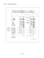
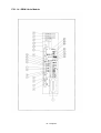
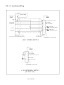
FIG. 1.1 - Inter module wiring
230 VAC
3 x 230 Vac
9 - 6/July/98
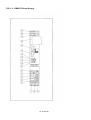
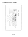
FIG. 1.2 - DBM-PS Power Supply
10 - 6/July/98
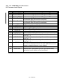
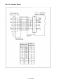
Tab. 1.1 - DBM-PS Power Supply (See Fig. 1.2)
Pos.
1
2
3
4
5
6
7
8
9
10
11
12
13
14
15
16
17
18
19
Name
R
S
T
GND
RR
RR
AUX
AUX
Yellow LED
PWR-BUS
Red LED
DBR FAULT
N.C.
Red LED
OVER
TEMP
Green LED
AUX
POWER
J2
J10
J1
GND
LL+
"L1" phase, three-phase input voltage 230Vac
"L2" phase, three-phase input voltage 230Vac
"L3" phase, three-phase input voltage 230Vac
Ground
Recovery resistor
Recovery resistor
Auxiliary power supply 230Vac (110Vac as option)
Auxiliary power supply 230Vac (110Vac as option)
BUS BAR voltage > 40Vdc
Recovery unit fault
Module overtemperature via PTC (threshold 80 °C)
Auxiliary power supply OK
RS485 output port to drives and power control fault
RS485 input port
Auxiliary power supply flat connector
Ground
BUS BAR -HV 300Vdc
BUS BAR +HV 300Vdc
11 - 6/July/98
Tab. 1.2 - DBM-PS Power Supply - J1 Connector
Auxiliary Power Supply
Pos.
1
2
3
4
5
6
7
8
9
10
11
12
13
Name
N.C. (Not connected)
N.C.
- 15Vdc referred to -HV (300Vdc)
+18Vdc referred to -HV (300Vdc)
150kHz square wave to high side drives
N.C.
+18Vdc referred to logic 0V
- 18Vdc referred to logic 0V
+8Vdc referred to logic 0V
+8Vdc referred to logic 0V
Logic 0V
Resolver 0V
10 kHz sinusoidal wave for resolver and synchronism (carrier)
Tab. 1.3 - DBM-PS Power Supply - J2 Connector
RS485 Port Signal and PWRS Control
Pos.
1
2
3
4
5
6
7
8
9
Name
+ Rx (RS485 serial link)
N.C.
+ Tx (RS485 serial link)
PWRS fault 1 - power supply binary coded faults (level 1)
+ 5Vdc input referred to logic 0V
- Rx (RS485 serial link)
Logic 0V
- Tx (RS485 serial link)
PWRS fault 2 - power supply binary coded faults (level 2)
Note: Rx and Tx are the receiving and transmitting signals with reference to the drive. In the
rest of the manual "RS485 serial link", referring to Rx and Tx, will not be specified anymore.
12 - 6/July/98
In case of fault, the type of fault is as follows:
J2/pos. 4
0
0
1
1
J2/pos. 9
0
1
0
1
OK
DBR FAULT. Recovery fault
OVER TEMP. Overtemperature
PHASE FAULT.
Tab. 1.4 - DBM-PS Power Supply - J10 Connector
RS485 Port
Pos.
1
2
3
4
5
6
7
8
9
Name
+Rx
N.C.
+Tx
N.C.
+5Vdc output referred to logic 0V for power supply
-Rx
Logic 0V
-Tx
N.C.
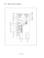
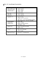
FIG. 1.A - DBM-PS Card Jumpers
1.8A DBM-PS Internal Card
Jumpers
JP1 closed (default) = connects a 120 Ω
resistor between RX+ and RX-.
JP2 closed (default) = connects TX- of
serial link to 0V via pull-down resistor
JP3 closed (default) = connects TX+ of
serial link to +5V via pull-up resistor
13 - 6/July/98
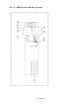
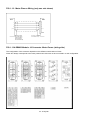
FIG. 1.3 - DBM 3-Axis Module
14 - 6/July/98
FIG. 1.4 - DBM 2-Axis Module
15 - 6/July/98
FIG. 1.5 - DBM 2-Axis and Expansion (optional) Module
16 - 6/July/98
FIG. 1.6 - DBM-L (180 mm) 3-Axis Module
17 - 6/July/98
FIG. 1.7 - DBM-L (180 mm) 2-Axis Module
18 - 6/July/98
FIG. 1.8 - EBM Expansion Module (optional)
19 - 6/July/98
Tab. 1.5 - DBM Axis Module (See Fig. 1.3 to 1.8)
Pos.
1
2
3
4
5
6
7
Name
J9
J6 M3
J5 M2
J4 M1
J8
J7
Red LED
DRFV
8
Red LED
WTD
Red LED
RF3
9
10
Red LED
RF2
11
Red LED
RF1
12
Red LED
OVT3
Red LED
OVT2
Red LED
OVT1
Trimmer
ILIMIT
Push
button
RESET
Red LED
DRV OVT
Red LED
SHRT CCT
Red LED
SHRT CCT
Red LED
SHRT CCT
J2
J3
13
14
15
16
17
18
19
20
21
22
23
Motor phases (M1-M2-M3) connector
Resolver M3 connector
Resolver M2 connector
Resolver M1 connector
I/O signals connector
connector for analog references and simulated encoder output
generic fault: the fault can correspond, according to the type, to a
LED on the front end; if other red LED's are not on, out of the
considered one, it is necessary to interrogate the drive via serial
link to know the fault reason (see FA command)
Watch dog - signal; microprocessor circuit faults; this LED is on
during reset
Resolver 3 fault - signal; resolver M3 fault, sin /cos signals
interrupted, short circuit between signals or 10kHz carrier
abnormal
Resolver 2 fault - signal; resolver M2 fault, sin /cos signals
interrupted, short circuit between signals or 10kHz carrier
abnormal
Resolver 1 fault - signal; resolver M1 fault, sin /cos signals
interrupted, short circuit between signals or 10kHz carrier
abnormal
Motor M3 overtemperature
Motor M2 overtemperature
Motor M1 overtemperature
all axes peak current control (only for setup technicians); if current
limit is required see IL, DL, AL commands
digital control card reinitialization
module overtemperature
short circuit on axis 1 (motor phases)
short circuit on axis 2 (motor phases)
short circuit on axis 3 (motor phases)
RS485 input port and PWRS-fault signals connector
Expansion connector for two axis module; on three axis module
some pins of this connector are used as test points
Green LED Reference enabled - signal: three - axis speed reference enable
REF EN (see Tab. 1.12/ pos. 16)
20 - 6/July/98
24
25
26
27
28
29
30
31
32
33
Green LED
DRIVE
EN 1
Green LED
DRIVE
EN 2
Green LED
DRIVE
EN 3
Green LED
POWER
OK
J1
GND
LL+
J10
Axis 1 enable (see also ON command)
Axis 2 enable (see also ON command)
Axis 3 enable (see also ON command)
Auxiliary power OK
Personality card: it contains drive setup in a non volatile memory
Auxiliary power supply flat connector
Ground
BUS BAR -HV 300Vdc
BUS BAR +HV 300Vdc
Motor phases (M1-M2-M3) connector for DBM-L module
Tab. 1.6 - DBM Module, EBM Expansion - J1 Connector
Auxiliary Power Supply
Pos.
1
2
3
4
5
6
7
8
9
10
11
12
13
Name
N.C.
N.C.
- 15Vdc referred to -HV (300Vdc)
+ 18Vdc referred to -HV (300Vdc)
150kHz square wave to high side drives
N.C.
+ 18Vdc referred to logic 0V
- 18Vdc referred to logic 0V
+ 8Vdc referred to logic 0V
+ 8Vdc referred to logic 0V
Logic 0V
Resolver 0V
10kHz sinusoidal wave for resolver and synchronism (carrier)
21 - 6/July/98
Tab. 1.7 - DBM Module - J2 Connector Power Supply Flat and RS485 Port Signals
Pos. Name
1
2
3
4
5
6
7
8
9
+Rx
N.C.
+Tx
PWRS fault 1 - power supply binary coded faults
+5Vdc output referred to logic 0V
-Rx
logic 0V
-Tx
PWRS fault 2 - power supply binary coded faults
Note: In case of fault, the type of fault is as follows:
J2/pos. 4 J2/pos. 9
0
0
0
1
1
0
1
1
OK
DBR FAULT. Recovery fault
OVER TEMP. Overtemperature
PHASE FAULT.
22 - 6/July/98
Tab. 1.8 - DBM Module - J3 Connector
Expansion Connection
Pos. Name
1
2
3
4
5
6
7
8
9
10
11
12
13
14
15
0V common
Auxiliary voltages referred to logic 0V not OK input signal
Phase U reference current output signal
Torque enabled output signal
Short circuit input signal
Overtemperature input signal
Expansion present input signal
Overtemperature output signal
N.C.
Phase V reference current, output signal
Overtemperature input signal
Non - coherent current input signal
BUS BAR fault input signal
Auxiliary voltages referred to - HV (300Vdc) not OK, input signal
N.C.
23 - 6/July/98
FIG. 1.9 - Limit Switches Wiring
DBM 04
1
0V
2
C W L im it sw itch a xis 1
5
C C W L im it sw itch a xis 1
6
C W L im it sw itch a xis 2
12
C C W L im it sw itch axis 2
13
C W L im it sw itch a xis 3
14
C C W Lim it s w itc h a x is 3
ca b le sh ield m us t b e R F *
co n ne cte d to g ro un d
*=see Section 6
J3
g ro u n d in g o f s h ie ld
v ia co n n e cto r s h e ll
24 - 6/July/98
Tab. 1.9 - DBM Module J3 Connector (when EBM Expansion is not present)
Limit Switches Connection (see Fig. 1.9)
The J3 connector allows, when the Expansion is not present, the availability of CW/CCW limit
switches for each axis. With the input enabled (to 0V), the rotation is disabled in one direction
and enabled in the other direction.
When the Expansion is present, the J3 connector is used for signal connection to the
Expansion module.
Pos. Name
1
2
3
4
5
6
7
8
9
10
11
12
13
14
15
0V common
CW limit switch, axis 1
N.C.
N.C.
CCW limit switch, axis 1
CW limit switch, axis 2
N.C.
N.C.
N.C.
N.C.
N.C.
CCW limit switch, axis 2
CW limit switch, axis 3
CCW limit switch, axis 3
0V common
Note: CW means clockwise rotation when viewed from shaft end, with default DI command.
25 - 6/July/98
Tab. 1.10 - DBM Module - J4 - J5 - J6 Connectors
Resolvers
Pos.
1
Name
cos
Differential cos signal non-inverted input
2
cos
Differential cos signal inverted input
3
4
Shield
sin
Internally connected to 0V common
Differential cos signal non-inverted input
5
sin
Differential cos signal inverted input
6
7
8
9
PTC
0V
PTC
V ref
Motor PTC input
0V common. Special for 10kHz carrier
Motor PTC input
20 Vpp/ 10kHz sinusoidal output signal for supplying primary
resolver winding (carrier)
26 - 6/July/98
FIG. 1.10 - Speed Reference Wiring
DBM 04
C NC
REF
REF
0V
0V
J7
c a b le sh ie ld m u s t b e R F
c o n n e cte d to th e h o u s in g
g ro u n d in g o f sh ie ld
v ia c o n n e c to r sh e ll
D IF F E RE N T IA L IN P U T
D B M 04
CNC
REF
0 V
REF
0 V
J7
c a b le s h ie ld m u s t b e R F
c o n n e c te d to th e h o u s in g
g ro u n d i n g o f s h i e ld
v ia c o n n e c to r s h e ll
U N IP O L A R IN P U T
27 - 6/July/98
Tab. 1.11 - DBM Module - J7 Connector
Analog Inputs and Simulated Encoder Outputs
Pos.
1
Name
2
3
4
5
6
7
8
9
10
11
12
A1
B1
C1
A2
B2
C2
A3
B3
C3
TP2
ILIMIT3
13
14
15
16
ILIMIT2
ILIMIT1
17
REF2
18
REF1
19
20
21
22
23
24
25
26
27
28
A1
B1
C1
A2
B2
C2
A3
B3
C3
REF3
Logic 0V (it can be used as common for analog output
supplies ±15V)
encoder output: inverted phase A - motor 1
encoder output: inverted phase B - motor 1
encoder output: inverted phase C - motor 1
encoder output: inverted phase A - motor 2
encoder output: inverted phase B - motor 2
encoder output: inverted phase C - motor 2
encoder output: inverted phase A - motor 3
encoder output: inverted phase B - motor 3
encoder output: inverted phase C - motor 3
Testing point 2
Analog input I limit axis 3, referred to analog 0V
0V = zero current
+10V (or not connected) = max current
Analog input I limit axis 2, referred to analog 0V (0 to +10V )
Analog input I limit axis 1, referred to analog 0V (0 to +10V )
Shield. Internally connected to 0V
Differential inverting analog input for the speed reference
signal (or torque ref. signal, see TC command) axis 3, max
range ±10V (see MR command). See Fig. 1.10.
Differential inverting analog input for the speed reference
signal (or torque ref. signal, see TC command) axis 2, max
range ±10V (see MR command). See Fig. 1.10.
Differential inverting analog input for the speed reference
signal (or torque ref. signal, see TC command) axis 1, max
range ±10V (see MR command). See Fig. 1.10.
+15Vdc output (I max = 30mA)
encoder output: phase A - motor 1
encoder output: phase B - motor 1
encoder output: phase C - motor 1
encoder output: phase A - motor 2
encoder output: phase B - motor 2
encoder output: phase C - motor 2
encoder output: phase A - motor 3
encoder output: phase B - motor 3
encoder output: phase C - motor 3
28 - 6/July/98
29
30
31
TP1
DRIVE
OK 1
32
DRIVE
OK 2
33
DRIVE
OK 3
34
REF3
35
REF2
36
REF1
37
Testing point 1
Shield. Internally connected to 0V
Drive OK output, axis 1. Imax=5mA.
0V=not OK
+5V=OK
Drive OK output, axis 2. Imax=5mA.
0V=not OK
+5V=OK
Drive OK output, axis 3. Imax=5mA.
0V=not OK
+5V=OK
Differential non-inverting analog input for the speed reference
signal (or torque ref. signal, see TC command) axis 3, max
range ±10V (see MR command). See Fig. 1.10.
Differential non-inverting analog input for the speed reference
signal (or torque ref. signal, see TC command) axis 2, max
range ±10V (see MR command). See Fig. 1.10.
Differential non-inverting analog input for the speed reference
signal (or torque ref. signal, see TC command) axis 1, max
range ±10V (see MR command). See Fig. 1.10.
- 15Vdc output (I max = 30mA)
REMARK: in DBM 01 version positions 31, 32 and 33 were assigned to differential inverting
I Limit analog inputs. If this option was used, to change DBM 01 with DBM 03 it is necessary
to properly specify differential analog I Limit input in the order (CG5502 code).
29 - 6/July/98
FIG. 1.11- Input/Output Wiring
+24V
+ 24V Pow er Supply
0V
D BM
CNC
+2 4 V
0V
8
D rive E n ab le
*
R e f. E n a b le
16
D rive O K
10
M o to r O K
12
O p to isola te d inp u t co m m o n
D rive E n ab le
R e fe re nce E n a b le
D rive OK
O p to iso la te d O u tp u t
9
M o to r O K
O p to iso la te d O u tp u t
11
g ro u n d in g o f sh ie ld
via h o se cla m p
ca b le sh ie ld m u st b e R F
co n n e cte d to th e h o u sin g
J8
* = p in n u m b e r is a xis de pe n de n t
+ 2 4 V P O W E R SU P P L Y
DBM
6
0V C om m on
7
+ 15 V d c o utp u t
8
O p to isola ted inp u t co m m o n
*
D rive E n able
16
R e fe re nce E n a b le
J8
* = pin n u m b e r is a xis d ep e nd e n t
+ 1 5 V IN T E R N A L SU P P L Y
(fo r d rive test)
30 - 6/July/98
Tab. 1.12 - DBM Module J8 Connector
I/O Commands and Signals
Pos.
1
2
3
4
5
6
7
8
9
10
11
12
13
14
15
16
17
18
Name
TACHO TEST 1
TACHO TEST 2
TACHO TEST 3
ANALOG OUT 1
tachometer analog output, axis 1. Range: see ET command
tachometer analog output, axis 2. Range: see ET command
tachometer analog output, axis 3. Range: see ET command
analog output 1. Max current, velocity reference or velocity
error outputs. See ES and SO commands.
ANALOG OUT 2 analog output 2. Max current, velocity reference or velocity
error outputs. See ES and SO commands.
0V
0V common
+15V
+15Vdc output (Imax = 30mA)
OPTO 0V
Optoisolated 0V
DRIVE OK
Collector of Drive OK optoisolator
Emitter of Drive OK optoisolator
DRIVE OK
MOTOR OK
Collector of Motor OK optoisolator
Emitter of Motor OK optoisolator
MOTOR OK
DRIVE EN1
Drive enable 1: optoisolated input for axis 1 torque enable.
See Fig. 1.11.
DRIVE EN2
Drive enable 2: optoisolated input for axis 2 torque enable.
See Fig. 1.11.
DRIVE EN3
Drive enable 3: optoisolated input for axis 3 torque enable.
See Fig. 1.11.
REF EN
Reference enable: optoisolated input for the confirmation of
the common reference to the three axis (REF EN not active
means no speed reference or zero torque)
N.C.
REM RESET
Remote reset: optoisolated input for logic section reset,
equivalent to push button on the front panel
31 - 6/July/98
Tab. 1.13 - EBM Expansion (optional) - J3 Connector
(See Fig. 1.8)
Pos. Name
1
2
3
4
5
6
7
8
9
10
11
12
13
14
15
0V common
Auxiliary voltages referred to logic 0V not OK output signal
Phase U reference current input signal
Torque enabled input signal
Short circuit output signal
Overtemperature output signal
Expansion present input signal
Overtemperature input signal
NC
Phase V reference current, input signal
Overtemperature output signal
Non - coherent current output signal
BUS BAR fault output signal
Auxiliary voltages referred to +HV (300Vdc) not OK output signal
N.C.
32 - 6/July/98
Tab. 1.14 - Input/Output Characteristics
Optoisolated inputs
Drive enable 1,2,3
Reference enable
Remote reset
Optoisolated outputs
Drive OK
Motor OK
Analog tacho
outputs 1,2,3
Analog outputs
Analog Out1
Analog Out2
Velocity reference
inputs 1,2,3
Drive OK outputs
1, 2, 3
Simulated Encoder
differential output
z in =1.2 kΩ
I nom = 10 mA
Imax = 20 mA
Vmin = 15Vdc
Vmax = 25V
z out = 1.2 kΩ
I max = 20 mA
Vnom < 25 Vdc
z out = 100 Ω
I max = 5 mA
Range: see ET command
Gain error = ±10% over production spread
Max linearity error: ±2% over full range
z out = 100 Ω
I max = 10 mA
Range: see ES command
Full scale = ±10V
z in > 20 kΩ
Range = see MR command
Vmax = 12 V
TTL compatible
Fan-out = 5 LS-loads
I max = 5 mA
z out = 100 Ω
Full scale = 7V (differential)
33 - 6/July/98
FIG. 1.12 - Motor Phases Wiring (only one axis shown)
DBM 04
M otor
U
U
V
V
W
W
g ro u n d
g ro u n d
J9/J10/J11
grounding of shield
via connector clamp
(or RF connection to
the ground screw in
case of terminal board)
grou n din g of s hie ld
via connector clam p
FIG. 1.13A DBM03 Module. J9 Connector. Motor Power (wiring side)
The configuration of this connector depends on the different combinations of sizes .
Notes: M1 always corresponds to the more powerful axis. M3 must not be connected in 2 axis configuration.
34 - 6/July/98
FIG. 1.13B DBM03-L (180 mm) Module. J9 and J10 connectors. Motor Power (wiring
side)
The configuration of these connectors depend on the different combinations of sizes .
Notes: M2 always corresponds to the more powerful axis. M3 must not be connected in 2 axis configuration. For
U-V-W positions see Fig. 1.13A.
35 - 6/July/98
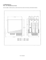
1.9 Dimensions
FIG. 1.14 - Dimensions (in mm).
Note: for DBM-L modules (180 mm), dimensions are the same as two side by side standard modules
36 - 6/July/98
1.10 Fans
The ventilation is provided by fans mounted under the modules. The size and the number of
fans are according to the system configuration.
Fan input voltage is 230 Vac (or 110 Vac optional). The input power is 60 W for each pair of
fans.
CAUTION: a free circulation must be guaranteed for the air flow.
TAB. 1.15 - FANS.
MODEL
DBM F2
DBM F3
DBM F4
DBM F5
DBM F2 (110V)
DBM F3 (110V)
DBM F4 (110V)
DBM F5 (110V)
INPUT
VOLTAGE
(V∼)
PAIR
OF
FANS
230
230
230
230
110
110
110
110
1
1
2
3
1
1
2
3
CONFIGURATION
DBM-PS + 1 DBM
DBM-PS + 2 DBM
DBM-PS + 3 DBM
DBM-PS + 4 DBM
DBM-PS + 1 DBM
DBM-PS + 2 DBM
DBM-PS + 3 DBM
DBM-PS + 4 DBM
Note: to size the fans a DBM-L (180 mm) module counts as two DBM modules.
Example: DBM-PS, one DBM module and one DBM-L (180 mm) module, requires a DBM F4
fan type.
1.11 Recovery Circuit
The recovery circuit is formed by a switching regulator, a recovery transistor and a recovery
resistance. While braking the motor returns energy which cannot be sent to the line since the
rectifier circuit is not regenerative. Returned energy tends to increase the BUS BAR DC
voltage. When HV reaches 375V the switching regulator brings the recovery transistor into
conduction, thus connecting the recovery resistance in parallel with filter capacitors. The
recovery resistance is formed by enameled wire fixed resistor(s).
37 - 6/July/98
If the recovery resistance works for intervals shorter than the time necessary to reach thermal
equilibrium, the resistor can temporarily handle power levels up to 10 times the nominal
power rating of the resistor (short time overload).
If not specifically requested, systems are provided with standard 3.9 Ω, 370W recovery
resistor.
An oversized Power Supply with three 8.2 Ω, 370 W (parallel configuration) is available.
WARNING: an unusual application with motor driven by the load, a large portion
of the time, could result in overheating of the recovery resistor.
An unusual application with motor driven by high inertial load from
high velocity in very short deceleration time could result in the
explosion of the input capacitor.
It is suggested contacting our Customer Service.
WARNING: do not touch recovery resistor during operation to avoid scalds.
Ventilated enclosures containing dynamic braking resistors shall
provide a degree of protection of at least IP22 (according to EN
60204-1, par. 13.3).
1.12 Standard Configurations
The modules are available in almost all combinations in the multiple version (see Fig.1.13A
and 1.13B).
We recommend to contact our Sales Locations or Service Centers for guidance on correct
selection of drives.
38 - 6/July/98
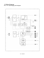
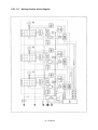
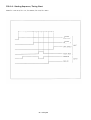
1.13 Block Diagrams
FIG. 1.15 - Power Supply, block diagram
39 - 6/July/98
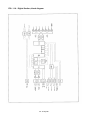
FIG. 1.16 - Digital Section, block diagram
40 - 6/July/98
FIG. 1.17 - Analog Section, block diagram
41 - 6/July/98
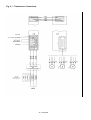
Fig. 2.1 - Transformer Connections
230 VAC
42 - 6/July/98
Section 2 - Installation
2.1 Wiring
This section provides the necessary information to properly wiring the digital brushless
system.
1.
2.
3.
4.
Mains connections via transformer or autotransformer.
Resolver and motor power wiring.
Signals wiring.
Other wiring.
2.1.1 Mains Connections via Transformer or Autotransformer
Figure 2.1 shows the electric diagram for transformer or autotransformer connection (from
three-phase mains voltage to 230V). See Appendix D for a correct sizing.
If a transformer is used it is recommended to set the - HV to the ground, the secondary
neutral remaining floating. It is recommended to use star primary winding and delta
secondary winding.
If an autotrasformer is used, the -AT must not be connected to the ground.
REMARK:
the auxiliary supply must be independent from the power supply, if the fault
information (see FA command) is to be retained in case of a mains failure.
43 - 6/July/98
Fig. 2.2 - Soft Start
44 - 6/July/98
2.1.2 Soft Start
Figure 2.2 shows a current limit circuit for a standard configuration (1 Power Supply and 3
modules): it is not strictly necessary for the system operation, though it is recommended to
limit the current through R-S-T phases on power up, as filter capacitors at power supply input
are uncharged and can require very high instantaneous current.
The three limit resistors must be short-circuited after 150 to 200 ms. They must be of high
energy type (to charge/uncharge capacitors) and must be rated 10 to 20 Ω, 100W.
The delay can be achieved by a timer (CR2 in Fig. 2.2) or by the circuit marked CR1 in
Fig. 2.2. In this case the component list is as follows:
Cc
Cd
F1, F2
K1
Rc
Rd
T2
: capacitor 0.1 µF, 250V
: electrolytic capacitor 20 µF, 250V
: fuse 315 mA,- 250V
: bridge rectifier 1A, 400V
: resistor 22 Ω, 5 W
: resistor 10 kΩ, 5 W
: relay SPST 5A, 220V, coil 110 V, 10 kΩ
45 - 6/July/98
FIG. 2.3 - Resolver Wiring
grounding of
shield via
grounding of shield
via connector clamp
46 - 6/July/98
2.1.3 Resolver Wiring
Each DBM module can be connected up to 3 resolvers via the following connectors:
J4 M1 : axis 1 resolver
J5 M2 : axis 2 resolver
J6 M3 : axis 3 resolver
A cable with 4 pair, each pair twisted and individually shielded with an independent overall
shield is recommended. 22 AWG ( 0.38mm2 ) to 20 AWG ( 0.6 mm2 ) can be used.
Resolver cables must be separated from power cables by a distance of 30cm (12 inches) by
using a independent duct (conduit). It is recommended to avoid intermediary connections for
resolver cables.
Figure 2.3 shows the wiring lay-out of the resolver with differential output.
2.1.3 Motor Power Wiring
There are seven different motor power connections, depending on module configuration (See
Fig. 1.12 and 1.13).
REMARK: motor power cables must be shielded.
2.1.5 Signals Wiring
All the enable signals and OK signals must be connected.
REMARK: it is suggested to connect the isolated output "DRIVE OK" to a remote control
switch so that, if a fault occurs, the power supply is disconnected to avoid system
damages.
2.1.5.1 Simulated Encoder Signals Wiring
Encoder signals cable must be shielded. For lengths in excess of 5 m (16 ft.) the cable must
have 3 pairs, each pair twisted.
REMARK: in noisy environments it is suggested to connect a 220 ÷ 680 Ω resistor between
A and A, B and B, C and C at the receiver input.
2.1.6 Serial Link Wiring
CAUTION: the serial link must be shielded and must be separated from the
power cable through the use of independent duct (conduit).
47 - 6/July/98
2.1.7 Serial Link Connection
REMARK: for the first installation it is strongly recommended to use either the
optional keypad or the DBTALK communication program.
2.1.7.1 Keypad
The keypad is an optional accessory product which can be used for drive setup and
monitoring. It must be connected to J10 connector.
If problems occur when attempting to communicate, the keypad is most likely set incorrectly.
To start the setup procedure press <CTRL>, then <CR>. For each parameter the current
setting is displayed, together with a question asking if you want to change it.
The correct setting is:
BAUD = 9600
WORD = 8D+E+1 STOP
BLOCK MODE
SINGLE LINE MODE
FLASHING OFF
KEY REPEAT ON SLOW
Be sure to save at the end of the procedure by pressing <Y> when the display shows: "Make
changes permanent Y/N".
2.1.7.2 DBTALK Communication Program
See Appendix B.
2.1.8 Other Wiring
•
•
•
•
the braking resistor
the flat cable for auxiliary supplies
the keyboard (or PC)
all the analog references
2.2 Installation
2.2.1 Starting Sequence
• Connect 230 Vac (or 110 Vac) single phase power supply.
• Multimodule configuration only. Disconnect the first module from the serial link and assign
basic address to the second module and so on for the next modules (all the modules from
factory being usually configured with address 1,2,3 if 3-axis or with address 1,2 if 2-axis).
Example of basic address assignment for the 2nd module, the first module being triple-axis:
FROM KEYBOARD (see Chapter 3 for a detailed description of commands)
1 SA 4 <CR>
Assign basic address 4 to the second module (its primary axis)
4 SV <CR>
Save the address configuration
48 - 6/July/98
Note: a module programmed as "address 4" will automatically assign for the other axes the
following addresses, i.e. 5 - 6 (if triple-axis) or 5 (if double-axis); and so on for the next basic
addresses.
• Check if NP (pole number), MV (max velocity) and MR (max reference) parameters are OK
for the application.
• Make a hardware reset via button on drive or via positive logic on pin 18 of J8 connector
(software reset via FA command being useless for digital control card reinitialization).
• Connect 230Vac three phase power supply.
WARNING: HIGH VOLTAGE - DISCHARGE TIME APPROX. 6 MINUTES.
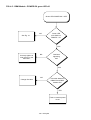
2.2.2 "Keyboard" or "Opto" Priority
On the personality card there is a jumper (G2) (See Fig. 2.4) which gives priority to keyboard
or to opto to execute "Drive Enable" command. " Drive Enable" opto isolated signals are
connected to J8/ pos.13, 14, 15.
G2 opened (position 2-3) = keyboard priority = the keyboard (or the device connected to the
serial link) is the master, i.e. it allows to enable or disable motor current, whereas the
optocouplers can only disable (protection); they can enable after resetting only.
The "Drive Enable" and "Reference Enable" opto-isolated signals must be driven at +15V.
Such a procedure, should be followed during installation and drive test.
G2 closed (position 1-2) =opto priority =the optocouplers are the master and the keyboard
can only be used for parameters setup.
Note: "Drive Enable" priority is different from the use of the analog or digital reference.
You can choose an analog or digital reference by "AR" (Analog) or "DR" (Digital) commands,
and save. The drives are supplied set to digital reference "DR".
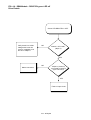
2.2.3 Autophasing
Note: it is possible to limit the current in autophasing via IL command.
• Check that the motor is free to rotate in both directions.
• Check that no fault condition occurs (red DRVF leds off).
•The jumper G2 on the personality card must be opened.
• Check that all module axes have analog drive enable on via positive logic and digital drive
enable off.
• Send the password command for the module.
• Send the autophasing command for every axis of the module and save.
49 - 6/July/98
Example for a double module with axis 4 and axis 5:
FROM KEYBOARD
4 PW91 <CR>
PASSWORD ON
<CR>
4 AP <CR>
AUTOPHASING IN PROGRESS
AXIS PHASED
5 AP <CR>
AUTOPHASING IN PROGRESS
AXIS PHASED
4 SV <CR>
Enter the password for 2nd module (primary axis = 4)
The correct answer is displayed
Only for optional keyboard.
Allow axis 4 autophasing.
Allow axis 5 autophasing.
Save module 4 phasing.
• Repeat the password and autophasing procedures for subsequent modules (if applicable).
• Make a hardware reset via button on drive or via positive logic on pin 18 of J8 connector.
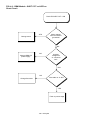
2.2.4 Wiring Checks
After phasing each axis, it is possible to check the wiring by rotating the motor via its digital
reference.
• Enable analog Drive Enable and Reference Enable via positive logic.
• Check that G2 is in position 2-3, for keyboard priority.
• Send to every axis the ON command (to enable digital Drive Enable) , the VE command
(for CW slow rotation), the VE- command (for CCW slow rotation), the OF command (to
disable the digital Drive Enable).
Example of checking axis 5 rotation:
FROM KEYBOARD
5 ON <CR>
O
5 VE 50 <CR>
5 VE-50 <CR>
5 OF <CR>
O
Enable digital Drive Enable for axis 5
Drive Enable led will be on
Set CW rotation at 50 rpm
Set CCW rotation at 50 rpm
Disable digital Drive Enable for axis 5
Drive Enable led will be off
50 - 6/July/98
2.2.5 CNC Priority
With CNC, the following procedures must be followed. This way the CNC is the master and
the keyboard is the slave, as follows:
• Parameters managed by CNC: Drive Enable, Reference Enable, Speed References
• Parameters managed by keyboard (or PC): all dynamic parameters (acceleration, KI, KP,
etc.), Status and Fault.
2.2.5.1 Setting of Analog References
To set the modules to use the analog references from the CNC, it is necessary to enter the
password, to send the AR command to every axis and to save. ST command can be entered
to check if the commands have been accepted.
Note that:
• AR command can be sent via global address (∗).
• If there are two or more modules, PW (password) and SV (save) commands can be sent to
each module (not only to each axis).
Example of enabling all the analog references for two modules with axes 1,2,3 and 4,5:
FROM KEYBOARD
1 PW91 <CR>
PASSWORD ON
4 PW91 <CR>
PASSWORD ON
* AR <CR>
1 SV <CR>
4 SV <CR>
1 ST <CR>
A1 ST___ E___ I_0___
...
Enter the password for 1st module (primary axis= 1)
The correct answer is displayed
Enter the password for 2nd module (primary axis = 4)
The correct answer is displayed
Enable analog reference for all axes
Save the configuration for 1st module
Save the configuration for 2nd module
Ask the status for axis 1
Axis 1 status is displayed. Check the 0 in the 2nd bit
after I (bit i)
Repeat ST command and check other axes
2.2.5.2 Drive Enable with CNC Priority
To give the priority for enabling and disabling the drive from the CNC, it is necessary to pull
out the personality card from the module, install G2 jumper in position 1-2 (closed) and to pull
in the card.
REMARK: if there are more than one module, do not swap the personality cards, this will
swap the module data.
51 - 6/July/98
2.2.6 Velocity Offset
If it is necessary you can adjust the analog velocity offset by providing 0 analog speed
reference and setting VO command for an automatic adjustment. A fine adjustment can be
done with successive steps via OV command.
REMARK: the adjustment of the digital velocity offset must not be used to adjust the analog
velocity offset and it is reserved to setup technicians. It can be made by providing 0 digital
speed reference (VE=0) and setting OC command. The opto Drive Enable must be high.
2.2.7 Personality Card Jumpers
WP (default: open): if closed, the EEPROM is write protected and SV command disabled
G1 (default: open) : if closed, connects TX- of serial link to 0V via pull-down resistor
G2
: if closed, gives priority to "opto" , if open gives priority to "keyboard"
G3 (default: open) : if closed, set 9600 Baud rate and basic address 1
G4 (default: open) : if closed, connects TX+ of serial link to 5V via pull-up resistor
G5 (default: open) : if closed, connects a 120 Ω resistor between RX+ and RX- of serial link
CAUTION: it is recommended to close the WP jumper at the end of installation
and setup.
Fig. 2.4 - Personality Card
Jumper open
Jumper closed
REMARK: personality card of DBM 03 has a software different from DBM 01 personality card.
To change DBM 01 with DBM 03:
1. Switch on DBM 03 with 230V mono-phase and replace the personality card with the old
DBM 01 personality card with G2 and G3 jumpers closed
2. Reset the drive with reset button on front panel
3. Wait 30 sec
4. Switch off the drive
5. Restore G2 and G3 as before the removal
The personality card is now set to DBM 03 format. New parameters are: 1SO=1; 2SO=2;
CU=128; CV=128; DF=0; ES=16; ET=80; PW=91, RN=RX=12; PR=3 and VS=0 for 2 pole
resolver; PR=1 and VS=1 for 6 pole resolver; SE=1024 (if applicable).
Note: - if the number of pulses per revolution has to be different from 1024, SE parameter
must be properly specified in the order
- after this setting the personality card cannot be used with DBM 01.
- with G2 and G3 closed DBM 03 does not work. The situation is as follows:
G2 open, G3 closed = keyboard priority, 9600 Baud, base address 1, password ON.
G2 and G3 closed = opto priority, reading of DBM 01 parameters (AC, AL/DL, AR/DR, BR, DE, IL,
IT, KI, KP, MR, MV, NP, OC, PC, RS, SA), password OFF.
52 - 6/July/98
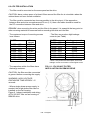
2.2.8 Resolver to Encoder (optional)
For position sensing a resolver to encoder option (simulated encoder) is available.
Encoder signals are 7V, 100 Ω impedance, as follows:
• 2 channels of square wave output with a resolution from 128 to 1024 pulses per electrical
revolution. Channel B leads channel A by 90° for clockwise rotation when viewed from
shaft end.
• 1 marker pulse per electrical revolution (i.e. 1∗ 3 = 3 marker pulses per mechanical
revolution with a 6 pole resolver).
• complementary outputs A, B and C .
FIG. 2.5 - Simulated Encoder (CW rotation when viewed from shaft end)
C h a n n el A
Channel B
C M a rk e r
Channel A
Channel B
C M a rk e r
53 - 6/July/98
2.2.8.1 Setup for the Number of Steps/Revolution
From DBM 03 version the number of steps/electrical revolution of simulated encoder can be
set via software (see SE commands).
REMARK: the maximum number of pulses per electrical revolution depends on the R/D
resolution. See Tab.2.1.
The width of C marker can be A (360°), A/2 (180°) or A/4 (90°); it must be specified in the
order. This parameter does not depend on the software commands.
Note: to obtain the resolution per mechanical revolution it is necessary to multiply the pole
pairs by the electrical resolution.
Example: if a FAS T motor with 6 pole resolver is used, 1024 pulses per electrical revolution
mean 1024 ∗ 3 = 3072 pulses per mechanical revolution.
54 - 6/July/98
2.2.8.2 R/D Resolution
From DBM 03 version the resolution of Resolver to Digital converter will automatically be
switched according to actual speed for optimum system performance between minimum (see
RN command) and maximum resolution (see RX command).
The speed range of R/D resolution is included in the following table.
Tab. 2.1 - Max speed and max ppr versus R/D resolution
Resolution (bit)
10
12
14
16
256
1024
4096
16384
Max speed with 2 pole
resolver (rpm)
24000
12000
3510
877
Max speed with 6 pole
resolver (rpm)
8000
4600
1170
292
Max speed with 8 pole
resolver (rpm)
6000
3510
877
219
Max number of pulses per
electrical revolution
55 - 6/July/98
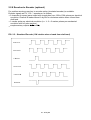
FIG. 2.6 - Starting Sequence, Timing Chart
Note: T1 = 8 to 10 s, T2 ≥ 1 s, T3 ≥ 20 ms, T4 ≈ 3 s, T5 ≥ 0.5 s.
230 Vac
230 Vac
56 - 6/July/98
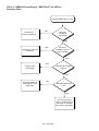
2.3 Operation
After system wiring and installation, it is possible to start the system according to the
sequence shown in figure 2.6.
Action
Effect
• Connect 230Vac single phase
power supply (or 110Vac
optional)
• Digital and diagnostics circuits
are fed
- Green LED on DBM PS, AUX PWR = ON
- Opto output MOTOR OK is enabled
• Connect 230Vac three phase
power supply
• 300V Bus Bars are fed
- Yellow LED on DBM PS, PWR BUS = ON
- Green LED on DBM, POWER OK = ON
• Reset protections by pushing
the RESET button on front
panel or by sending a 20ms
pulse to REM RESET opto input
• Possible faults are reset
- After 3s the opto output DRIVE OK is enabled
• Enable analog Drive Enable
for each axis and Reference
Enable via positive logic
• Green LED's on DBM, DRIVE EN = ON
and REF EN = ON
WARNING: HIGH VOLTAGE - DISCHARGE TIME APPROX. 6 MINUTES.
57 - 6/July/98
SECTION 3 - COMMANDS AND PROTECTIONS
3.1 General Features
For serial communication, according to standard RS485, DBM drives are connected in
parallel (multidrop) and in "slave" configuration, whereas the CNC, the PC or the keyboard
are in "master" configuration.
This is because the protocol is configured so that the drives are able to communicate only if
inquired by the master, to avoid contentions on the line. As a consequence, all the
commands have been configured individually (single axis questioned), except those for which
an answer is not foreseen; therefore all the drives can be reached simultaneously.
There are 3 kinds of command:
• status monitoring
Monitor commands on the status of the drive, which displays axis configuration and eventual
faults.
• data monitoring
Monitor commands for displaying memorized motion parameters (e.g. I limit=100%, etc.).
• data (command) input
Execute commands for setting and changing parameters (e.g. speed, pole number,
acceleration, deceleration, etc.).
Remark: if a mistake has been made while digitizing, it is possible to reset the command by
pressing <CR> ( <CARRIAGE RETURN> ).
The commands are in ASCII format:
1 bit-start
8 bit-data
1 bit-parity even
1 bit-stop
Serial communication speed can vary from 1200 to 19200 Baud.
58 - 6/July/98
Command syntax is as follows:
status monitoring:
data monitoring:
data input:
command input:
address COMMAND
address COMMAND
address COMMAND data
address COMMAND
Remark: press <CR> after each command string if the optional keyboard is used.
• Address: there are three kinds of address:
Axis: it is a number from 1 to 9 ( max. number of axes in a system); it identifies the axis
selected for data monitoring / input.
Module: the "module" (or "basic") address is referred to the possibility to get the execution of
the command either addressing the chosen axis (axis) or any axis inside the module
(
module ). This last possibility is valid for all axes within a module common commands (e.g.
temperature).
Global: it is also possible to globally address all axes (global address) using the <∗> in place
of the address number.
• Command: it consists of two letters (e.g. AC, AE, etc.).
• Datum: it can be composed by a max. of 4 figures or 3 figures and the <-> symbol. The
<+> symbol is optional. Any data without a symbol is considered as positive.
59 - 6/July/98
3.2 Commands
All commands available for system management can be used to monitor and execute every
datum.
To monitor, it is sufficient to enter the address and the command; to execute, the address,
the command and the datum must be typed.
Tab. 3.1 List of Commands
Symbol
Command
Symbol
Command
AC
AD
AE
AL
AP
AR
AS
BR
CP
CU
CV
DE
DF
Acceleration
Axis disabled
Axis enabled
Analog limit
Autophasing
Analog reference
Address show
Baud rate
Current position
Current U offset
Current V offset
Deceleration
Digital velocity
reference filter
Direction
Digital limit
Digital reference
Extra parameter
for spare output
Extra parameter
for Tacho output
Error velocity
Fault
I Limit
IT protection
Integral gain
Proportional gain
Max reference
MV
NP
OC
OF
ON
OV
PC
PR
Max velocity
Number of poles
Velocity Fine offset
Off
On
Offset Display
Peak current
Motor poles to
resolver poles ratio
Password
A/D resolution
Minimum of R/D
resolution
Resolver shaft
Maximum of R/D
resolution
Set Address
Simulated encoder
Spare output
Show Release
Status
Save
Torque Control
Velocity Control
Velocity
Velocity Offset
Velocity structure
DI
DL
DR
ES
ET
EV
FA
IL
IT
KI
KP
MR
PW
RE
RN
RS
RX
SA
SE
SO
SR
ST
SV
TC
VC
VE
VO
VS
60 - 6/July/98
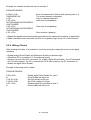
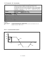
3.2.1 Command: AC - Acceleration
Function:
Syntax:
Address type:
Unit of measure:
Range:
Default:
Password:
(∗) addressing:
Opposite to:
See also:
Examples:
1 AC 100 <CR>:
2 AC <CR>:
it allows to set an acceleration ramp. Whatever the input
reference (analog or digital), the system will follow it, but
accelerations will never be faster than those set by this command. It
can be useful when the drive is connected to rather simple position
controllers ( e.g. max, 0, -max), with an application requiring
progressive accelerations.
data monitoring: address AC <CR>
data input:
address AC n <CR>
axis
n = ms
10 to 999 or 0
0 (disabled)
no
yes
DE
it sets an acceleration ramp = 100ms for axis1.
it questions axis 2 about the acceleration ramp. In case no one has been set, the
answer is: "A2 ACC. TIME = ms 0".
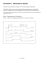
FIG. 3.1 - Acceleration/Deceleration
rpm
MV
DE
VE
ms
AC
DE
AC
61 - 6/July/98
3.2.2 Command: AD - Axis Disabled
Function:
Syntax:
Address type:
Unit of measure:
Range:
Default:
Password:
(∗) addressing:
Opposite to:
See also:
AD command makes the logic section ignore an axis and the
relatives faults. It is useful with DBM 2-axis: if the
third axis were not disabled, the logic would reveal resolver
fault and motor overtemperature, preventing the drive from
running.
data monitoring: address AD <CR>
data input:
address AD n <CR>
axis
n = axis number
1 to 99
yes
no
AE
AE
Note: the axis disabled holds his address, which can be interrogated via FA command.
REMARK: AD and AE commands must be set only when the motor is standstill
Examples:
1 AD 3 <CR>:
4 AD 6 <CR>:
1 AD <CR>:
it disables the 3rd axis of a module, whose first address is 1.
it disables the 3rd axis of a module, whose first address is 4.
"1 AXIS DISABLED 3" will be displayed if the 3rd axis is disabled. "1 AXIS DISABLED 1 3"
will be displayed if the 1st and 3rd axis is disabled.
3.2.3 Command: AE - Axis Enabled
Function:
Syntax:
Address type:
Unit of measure:
Range:
Default:
Password:
(∗) addressing:
Opposite to:
See also:
Examples:
1 AE 3 <CR>:
4 AE 6 <CR>:
1 AE <CR>:
the AE command enables an axis and relative faults.
data monitoring: address AE <CR>
data input:
address AE n <CR>
axis
n = axis number
1 to 99
yes
no
AD
AD
it enables the 3rd axis of a module, whose first address is 1.
it enables the 3rd axis of a module, whose first address is 4.
"1 AXIS ENABLED 3" will be displayed if the 3rd axis is enabled. "1 AXIS ENABLED 1 3"
will be displayed if the 1st and 3rd axis is enabled.
62 - 6/July/98
3.2.4 Command: AL - Analog Limit
Function:
Syntax:
Address type:
Unit of measure:
Range:
Default:
Password:
(∗) addressing:
Opposite to:
See also:
Examples:
1 AL <CR>:
it informs the controller that I limit reference to be considered is
analog (see J7 connector).
command input: address AL <CR>
axis
digital I Limit
yes
yes
DL
DL, IL, ST
Sets the analog I limit for axis 1. The display is cleared. After this command a current
limit can be set via J7 connector, pos. 14 and 33 (range 0 to 10V).
The status can be interrogated via ST command.
REMARK: DBM 03 has the "Analog I limit" as standard.
3.2.5 Command: AP - Autophasing
Function:
Syntax:
Address type:
Unit of measure:
Range:
Default:
Password:
(∗) addressing:
Opposite to:
See also:
AP command allows resolver auto-phasing. As in this phase the
motor can rotate for a revolution fraction, it is opportune to make
sure it is free to rotate to avoid risk of friction, which could
compromise phasing accuracy. So, motor must be disconnected
from load.
command input:
address AP <CR>
axis
non-phased axes
yes
no
ON, OF
Note: To execute AP, all module axes must have optoisolated Drive Enable signals "on" and digital ones "off"
(see paragraph 2.2.3) via OF command. To execute AP, it is necessary that the "G2" jumper on the
personality card is in position 2-3 (open), which means priority from the keyboard (see paragraph 2.2.2.).
Examples:
1 AP <CR>: it allows axis 1 auto-phasing. During such operation (a few seconds) "AUTOPHASING IN
PROGRESS" will be displayed; when auto-phasing is successfully carried out "AXIS PHASED" will be
displayed, otherwise "ERROR IN AUTOPHASING" will be shown. If digital Drive Enable is enabled (ON) (see
above) the message "WARNING DRIVE EN. CLOSED" will appear. The auto-phasing is not allowed if a
fault is on. This case, the message displayed will be "ERROR: FAULT STATUS".
63 - 6/July/98
3.2.6 Command: AR - Analog Reference
Function:
Syntax:
Address type:
Unit of measure:
Range:
Default:
Password:
(∗) addressing:
Opposite to:
See also:
AR command allows enabling analog (speed or torque) reference.
pins, ignoring VE command given from keyboard.
command input:
address AR <CR>
axis
digital reference
yes
yes
DR
DR
Note: the status can be interrogated via ST command (bit I).
3.2.7 Command: AS - Address Show
Function:
Syntax:
Address type:
Unit of measure:
Range:
Default:
Password:
(∗) addressing:
Opposite to:
See also:
Examples:
∗ AS <CR>:
it allows display of the basic address of a module, if unknown. To
avoid simultaneous answers on the line from more than one
module, it is necessary that serial flat J2 is connected only between
power supply and the questioned module. It is different from
SA command, which is used to change basic address.
data monitoring: ∗ AS <CR>
no
compulsory
SA
if the "base" address for such a module is 1, the answer will be "ADDRESS MODULE 1".
64 - 6/July/98
3.2.8 Command: BR - Baud Rate
Function:
Syntax:
Address type:
Unit of measure:
Range:
Default:
Password:
(∗) addressing:
Opposite to:
See also:
Note:
it allows to change transmission speed of the serial link.
data monitoring: address BR <CR>
data input:
address BR n <CR>
module
n = Baud
1200, 2400, 4800, 9600, 19200
9600
yes
yes
-
To modify the Baud Rate alsoat keyboard side, it is necessary to type <Control> and after <CR>.
Type <Y> to change Baud Rate and after <CR>.
3.2.9 Command: CP - Current Position
Function:
Syntax:
Address type:
Unit of measure:
Range:
Default:
Password:
(∗) addressing:
Opposite to:
See also:
Examples:
2 CP <CR>:
it allows to know the position relative to electric revolution of the
resolver at start-up. It is used when the application requires to
know the absolute position.
data monitoring: address CP <CR>
axis
0 to 4096
no
no
-
Interrogates axis 2 about the current position. If the starting position is 4006, the
answer will be : "A02 CURRENT POSITION = 4006".
65 - 6/July/98
3.2.10 Command: CU - Current U offset (only for setup technicians)
Function:
Syntax:
Address type:
Unit of measure:
Range:
Default:
Password:
(∗) addressing:
Opposite to:
See also:
it allows to set the offset of U phase current
data monitoring: address CU <CR>
data input:
address CU n <CR>
axis
0 to 255
no
no
CV
Note: the CU command must be executed with digital Drive Enable disabled (via OF command) and the opto
Drive Enable enabled.
Examples:
2 CU <CR>:
Interrogates axis 2 about the offset of the U current. If U current offset is 128, the
answer will be : "A02 CURRENT U OFFSET = 128".
CAUTION: do not change CU parameter. A wrong set of CU increases torque ripple.
3.2.11 Command: CV - Current V offset (only for setup technicians)
Function:
Syntax:
Address type:
Unit of measure:
Range:
Default:
Password:
(∗) addressing:
Opposite to:
See also:
it allows to set the offset of V phase current
data monitoring: address CV <CR>
data input:
address CV n <CR>
axis
0 to 255
no
no
CU
Note: the CV command must be executed with digital Drive Enable disabled (via OF command) and the opto
Drive Enable enabled.
Examples:
1 CV <CR>:
Interrogates axis 1 about the offset of the V current. If V current offset is 128, the
answer will be : "A01 CURRENT V OFFSET = 128".
CAUTION: do not change CV parameter. A wrong set of CU increases torque ripple.
66 - 6/July/98
3.2.12 Command: DE - Deceleration
Function:
Syntax:
Address type:
Unit of measure:
Range:
Default:
Password:
(∗) addressing:
Opposite to:
See also:
Examples:
1 DE 100 <CR>:
1 DE <CR>:
it allows to set a deceleration ramp. Whatever the input reference
(analog or digital), the system will follow it, but deceleration's will
never be faster than those set by this command. It can be
useful when the drive is connected to a rather simple position
controller (e.g. max,0,-max), with an application requiring
progressive deceleration's (see Fig. 3.1).
data monitoring: address DE <CR>
data input:
address DE n <CR>
axis
n = ms
10 to 999 or 0
0 (disabled)
no
yes
AC
it sets a deceleration ramp = 100 ms for axis 1.
it questions axis 1 about the deceleration ramp. In case no one has been set, the
answer is: "A01 DECEL. TIME = ms 0"
67 - 6/July/98
3.2.13 Command: DF - Digital Filter
Function:
Syntax:
Address type:
Unit of measure:
Range:
Default:
Password:
(∗) addressing:
Opposite to:
See also:
it allows to set a low-pass digital filter. The filter reduces high
frequency noise and resonance's
When the Velocity Structure command is VS=0 or VS=1, the
velocity reference is filtered.
When the Velocity Structure command is VS=2 or VS=3, the
velocity error is filtered.
The value DF=0 switches the filter OFF
data monitoring: address DF <CR>
data input:
address DF n <CR>
axis
0 to 255. The filter bandwidth is:
f [Hz] = {ln[1/(1-DF/512)]}/(2π∗300 10-6)
0 (disabled)
yes
no
VS
Note: the DF command must be executed with digital Drive Enable disabled (via OF command) and the opto
Drive Enable enabled.
Examples:
2 DF 165 <CR>:
2 DF <CR>:
sets the filter bandwidth to 206 Hz for axis 2.
Interrogates axis 2 about the reference filter on the velocity reference. The answer will
be : "A02 DIG.FIL. REF. PAR. = 165".
Tab. 3.2 - Filter Bandwidth
DF Frequency DF Frequency DF Frequency DF Frequency
1
1 Hz
65
72 Hz
130
155 Hz
195
254 Hz
5
5 Hz
70
77 Hz
135
162 Hz
200
262 Hz
10
10 Hz
75
84 Hz
140
169 Hz
205
271 Hz
15
15 Hz
80
90 Hz
145
176 Hz
210
280 Hz
20
21 Hz
85
96 Hz
150
183 Hz
215
288 Hz
25
26 Hz
90
102 Hz
155
191 Hz
220
297 Hz
30
32 Hz
95
108 Hz
160
198 Hz
225
307 Hz
35
37 Hz
100
115 Hz
165
206 Hz
230
316 Hz
40
43 Hz
105
121 Hz
170
214 Hz
235
325 Hz
45
48 Hz
110
128 Hz
175
221 Hz
240
335 Hz
50
54 Hz
115
134 Hz
180
229 Hz
245
345 Hz
55
60 Hz
120
141 Hz
185
237 Hz
250
355 Hz
60
66 Hz
125
148 Hz
190
246 Hz
255
366 Hz
68 - 6/July/98
3.2.14 Command: DI - Direction
Function:
Syntax:
Address type:
Unit of measure:
Range:
Default:
Password:
(∗) addressing:
Opposite to:
See also:
Example:
4 DI <CR>:
it allows to invert the direction of the motor rotation, in case of
analog or digital reference. The drive is supplied set to CW
rotation, (viewed from shaft end) corresponding to positive
during the installation. To know what the actual configuration is,
ST command shall be asked.
command input:
address DI <CR>
axis
CW
no
yes
ST
it reverses the direction of motor rotation for axis 4. The display is cleared.
Note: The status can be interrogated via ST command (bit L).
3.2.15 Command: DL - Digital Limit
Function:
Syntax:
Address type:
Unit of measure:
Range:
Default:
Password:
(∗) addressing:
Opposite to:
See also:
Notes:
it informs the controller that the I limit reference to be considered as
active is digital (programmable via IL command).
command input:
address DL <CR>
axis
digital I limit
yes
yes
AL
AL, IL
Digital I limit is standard on DBM drives, whereas analog I limit is optional.
The status can be interrogated via ST command (bit J).
69 - 6/July/98
3.2.16 Command: DR - Digital Reference
Function:
Syntax:
Address type:
Unit of measure:
Range:
Default:
Password:
(∗) addressing:
Opposite to:
See also:
it allows to enable digital (speed or torque) reference. The drive
will consider as reference the number set via VE command and
ignore connector J7 voltage.
command input:
address DR <CR>
axis
digital reference
yes
yes
AR
AR
Note: the status can be interrogated via ST command (bit I)
70 - 6/July/98
3.2.17 Command: ES - Extra parameter for Spare output
Function:
Syntax:
Address type:
Unit of measure:
Range:
Default:
Password:
(∗) addressing:
Opposite to:
See also:
Examples:
1 SO 1 <CR>:
1 ES 16 <CR>:
1 ES 32 <CR>:
1 ES 8 <CR>:
2 SO 5 <CR>:
2 ES 16 <CR>:
it allows to scale the Analog Outputs (max current, speed reference
or error reference) on J8 connector.
data monitoring: address ES <CR>
data input:
address ES n <CR>
1=Analog Output 1 (see J8 connector, pos.4)
2=Analog Output 2 (see J8 connector, pos.5)
0 to 255. Analog outputs on J8 connector (±10V, 10 mA max):
Max current for axis 1 (SO=1), axis 2 (SO=2) or axis 3 (SO=3):
±(10∗ES/16)V for ±100% max current
Speed reference for axis 1 (SO=4), axis 2 (SO=5) or axis 3 (SO=6),
and velocity error for axis 1 (SO=7), axis 2 (SO=8) or axis 3 (SO=9):
±[(ES∗NP∗MV)/(786∗MR)]V for ±MV (max velocity)
16
yes
no
MR, MV, NP, SO
sets analog out1 (J8 conn., pos.4) to max current of axis 1
sets analog out1 to ±10V for ±100% max current of axis 1
sets analog out1 to ±10V for ±50% max current (zoom-in) of axis 1
sets analog out1 to ±5V for ±100% max current (zoom-out) of axis 1
sets analog out2 (J8 conn., pos.5) to speed reference of axis 2
sets analog out2 to ±10V for ±6140 rpm (if NP=8 and MR=100 have been set for axis 2)
Tab. 3.3 - ES for Max Current (SO=1 to SO=3)
ES
MAX
ANALOG
CURRENT
OUT
8
100 %
5V
16
100 %
10 V
32
50 %
10 V
Tab. 3.4 - ES for Speed Reference and Velocity Error (MR=100, SO=4 to SO=9)
2 pole resolver
ES
52
65
105
131
MV ANALOG
rpm
OUT
6046
8V
6046
10 V
2994
8V
3000
10 V
6 pole resolver
ES
17
22
35
44
52
65
MV
rpm
6165
5954
2994
2977
2015
2015
8 pole resolver
ANALOG
OUT
8V
10 V
8V
10 V
8V
10 V
71 - 6/July/98
ES
13
16
26
33
39
49
MV
rpm
6046
6140
3023
2977
2015
2005
ANALOG
OUT
8V
10 V
8V
10 V
8V
10 V
3.2.18 Command: ET - Extra parameter for Tacho output
Function:
Syntax:
Address type:
Unit of measure:
Range:
Default:
Password:
(∗) addressing:
Opposite to:
See also:
it allows to scale the Tacho Tests outputs on J8 connector
data monitoring: address ET <CR>
data input:
address ET n <CR>
axis
50 to 100. Tacho outputs = ±(ET/10) ∗ (MR/100) [V] for ±MV
80
yes
no
MR, MV
Examples:
1 MV 3000 <CR>: sets max velocity to 3000 rpm for axis 1.
1 MR 100 <CR>: sets max velocity reference to 10 V for axis 1.
sets ET parameter to 50 for axis 1. The Tacho Test 1 (J8, pos.1) will be ± 5V for
1 ET 50 <CR>:
± 3000 rpm.
questions axis 1 about the extra parameter for Tacho Test 1. The answer is: "A01 EXTRA
1 ET <CR>:
PAR. FOR TO = 50".
3.2.19 Command: EV - Error Velocity
Function:
Syntax:
Address type:
Unit of measure:
Range:
Default:
Password:
(∗) addressing:
Opposite to:
See also:
Remark:
it allows to set the maximum velocity error between reference
velocity and the actual speed in rpm. If the set value is overcome,
a fault occurs. Value = 0 disables the command.
data monitoring: address EV <CR>
data input:
address EV n <CR>
axis
n = rpm
1 to MV. 0 = disabled
0
yes
no
-
While testing the drives via step response, it is advisable to disable this protection or set a
high value of tolerated error, to avoid continuous faults.
Examples:
1 EV 100 <CR>:
3 EV <CR>:
it sets axis 1 to tolerate up to 100 rpm error, without fault.
it questions axis 3 about the maximum error allowed. The answer is: "A3 VELOCITY
ERROR RPM = 20" (if 20 rpm velocity error has been set for axis 3).
72 - 6/July/98
3.2.20 Command: FA - Fault
Function:
as only main faults have front panel LED indications, when the
generic LED DRVF lights up, it is necessary to interrogate
the drive via FA command. The answer is a codified ASCII string
(see below). Another function of the command is to reset the faults
status monitoring and reset: address FA <CR>
axis
no
no
Syntax:
Address type:
Password:
(∗) addressing:
Answer explanation: A a FA b c d e f g P h i j k l MA m n o B p q r
A
a
= axis
= axis address
FA
b
c
d
e
f
g
= fault
= Resolver connection
= Motor temperature
= Axis short circuit
= 3-phase sequence
= Velocity error
= It
P
h
i
j
k
l
= Power supply
= Recovery unit
= PWRS temperature
= 220Vac 3-phase sequence
= n.c.
= Personality card
MA
m
n
o
= A module (DBM module)
= BUS BAR voltage
= Aux. Volt. ref. to - HV
= A module temperature
B
p
q
r
0 = OK
0 = OK
0 = OK
0 = OK
0 = OK
0 = off
1 = not OK
1 = overtemperature
1 = short circuit
1 = not coherent phase
1 = not OK
1 = on
0 = OK
0 = OK
0 = OK
1 = not OK
1 = overtemperature
1 = unbalanced phase
0 = OK
1 = not OK*
0 = OK
0 = OK
0 = OK
1 = overvoltage/undervoltage
1 = out of tolerance
1 = overtemperature
= B module (eventual expansion module)
= BUS BAR voltage
0 = OK
= Aux. Volt. ref. to - HV
0 = OK
= B module temperature
0 = OK
1 = overvoltage/undervoltage
1 = out of tolerance
1 = overtemperature
* = in case of checksum error, check the parameters (e.g. KP, KI,...), correct the wrong values and save.
Note: If the expansion missing, the last characters are not significant.
Examples:
1 FA <CR>:
if OK, the answer will be: "A1 FA 000000 P 00000 MA 000 B 000"
73 - 6/July/98
3.2.21 Command: IL - I Limit (Current Limit)
Function:
Syntax:
Address type:
Unit of measure:
Range:
Default:
Password:
(∗) addressing:
Opposite to:
See also:
it allows to program the peak current. It is useful when
undersized motors are used or during special tests.
data monitoring: address IL <CR>
data input:
address IL n <CR>
axis
n = % max current
0 to 100
100
no
no
DL, AL
REMARK: before executing IL command it is necessary to perform DL command.
Examples:
2 IL <CR>:
2 IL 90 <CR>:
it asks axis 2 about I limit. In default case the answer will be: "A2 CURRENT LIMIT % =
100".
it sets 90% current limit for axis 2.
3.2.22 Command: IT - IT protection
Function:
Syntax:
Address type:
Unit of measure:
Range:
Default:
Password:
(∗) addressing:
Opposite to:
See also:
Notes:
it allows to manage the IT thermal protections which prevents the
motor from an overheating too quick for the PTC operating
time. When the integral of current multiplied by time exceeds the
IT value, drive limits, after operating time, to nominal motor
current (see Tab. 3.5).
data monitoring: address IT <CR>
data input:
address IT xx n <CR>. xx = special password
axis
n = ms
0 to 255. 0 = protection disabled
see Tab. 3.5
special password
no
PC
IT protections has been implemented from software version 3.5.
IT status can be interrogated via FA command (bit g).
CAUTION: do not change IT parameter. A wrong set of IT can damage the motor.
74 - 6/July/98
Tab. 3.5 - IT Protection
The following table shows IT and PC values set in factory.
MOTOR DRIVE
DBM03
FAS T0
M2 030
M2 060
"
M4 030
"
M4 060
"
M8 030
"
M8 060
"
FAS T1
M2 030
"
M2 060
"
M4 030
"
M4 045
M6 030
"
M6 045
"
M8 030
"
M8 045
FAS T2
M2 030
"
M2 045
"
M4 020
M4 030
"
M6 020
"
M6 030
M8 020
M8 030
FAS T3
M2 020
M2 030
M3 020
M3 030
M4 020
M4 030
"
M6 012
M6 020
"
M8 012
M8 020
"
IT
PC
Operating
time at drive
peak current
(s)
1.5
1.5
2.5
1.5
15
14
14
16
24
38
25
40
7.0
19.8
8.2
19.4
2.5
2.5
5
2.5
5
5
10
16
12
11
12
11
15
14
27
46
23
44
22
42
25
8.4
35.3
8.8
31.9
8.0
23
8.2
MOTOR
FAS K0
005 030
"
005 060
"
DRIVE
DBM03
IT
PC
Operating time
at drive peak
current
(s)
1.5
2.5
1.5
2.5
11
11
12
12
23
15
37
25
8.8
3.7
21.8
9.6
010 030
1.5
14
40
22.2
"
2.5
14
27
9.6
010 060
2.5
14
48
33.3
"
5
11
24
9.6
020 030
5
13
26
9.6
020 060
5
12
48
38.8
"
10
12
29
13.0
FAS K1
2.5
9
55
71.3
020 030
2.5
6
48
77.8
5
8
27
16.9
"
5
5
24
21.2
5
9
54
68.2
020 060
5
6
44
63.9
10
8
32
24.1
040 030
5
6
44
63.9
5
7
49
69.9
"
10
6
26
20.8
10
7
30
24.0
040 045
10
6
40
51.8
10
7
44
54.8
060 030
10
6
40
51.8
10
4
42
86.6
"
15
5
22
17.7
15
4
23
24.2
060 045
10
6
60
132.6
10
5
62
173.1
"
15
6
34
36.5
15
4
35
58.3
"
25
6
22
14.7
10
5
52
112.5
080 030
10
6
53
98.0
15
4
29
39.2
"
15
5
29
31.3
15
4
41
82.1
080 045
15
6
44
63.9
"
25
6
28
24.3
10
8
52
70.2
FAS K2
15
8
29
19.6
060 030
10
5
43
72.9
15
9
47
49.4
"
15
5
24
21.2
25
8
30
21.0
060 045
10
5
60
159.2
10
7
59
109.0
"
15
5
33
41.1
15
7
50
73.3
120 020
10
5
53
117.6
25
6
32
32.1
"
15
5
30
33.6
15
6
48
77.8
120 030
15
5
44
76.8
25
5
30
33.6
"
25
5
29
31.3
25
7
45
57.6
180 020
15
5
38
55.6
25
6
39
49.0
180 030
25
5
43
72.9
25
6
55
107.1
240 020
25
5
43
72.9
240 030
50
5
29
31.3
25
6
48
77.8
FAS K3
25
8
70
150.0
240 020
25
3
38
92.8
25
6
64
156.6
240 030
50
3
27
45.0
50
5
48
93.4
360 020
50
3
30
56.1
50
4
40
77.8
360 030
50
3
44
128.0
50
6
70
200.1
"
70
3
34
73.1
70
5
55
128.5
480 020
50
3
38
92.8
25
5
66
204.0
"
70
3
30
56.1
50
4
53
147.1
480 030
70
3
41
109.5
70
4
42
86.6
"
80
3
31
60.1
50
4
42
86.6
720 012
50
3
33
68.6
70
4
65
244.9
720 020
70
3
41
109.5
80
4
48
116.8
"
80
3
31
60.1
960 012
50
3
44
128.0
"
70
3
34
73.1
"
80
3
25
38.4
960 020
70
3
51
179.2
"
80
3
38
92.8
REMARK: the "operating time at drive peak current" is the operating time after a reset. In a steady state condition, this time can be shorter
according to the motor thermal simulation. An overtemperature protection via PTC is also provided.
75 - 6/July/98
3.2.23 Command: KI - Integral Gain
Function:
Syntax:
Address type:
Unit of measure:
Range:
Default:
Password:
(∗) addressing:
Opposite to:
See also:
Examples:
2 KI <CR>:
2 KI 50 <CR>:
it allows to set the speed loop integral gain. KI value is directly
proportional to the intensity of the integral action.
data monitoring: address KI <CR>
data input:
address KI n <CR>
axis
0 to 255
20
no
yes
KP
it asks axis 2 about KI. If it is 40, the answer will be "A4 KI = 40".
it sets the integral gain to 50 for axis 2
3.2.24 Command: KP - Proportional Gain
Function:
Syntax:
Address type:
Unit of measure:
Range:
Default:
Password:
(∗) addressing:
Opposite to:
See also:
Examples:
4 KI <CR>:
4 KI 50 <CR>:
it allows to set the speed loop error proportional correction gain. KI
value is directly proportional to the intensity of the requested action.
data monitoring: address KP <CR>
data input:
address KP n <CR>
axis
0 to 255
80
no
yes
KI
it asks axis 4 about KP. If it is 90 the answer will be "A04 KI = 90".
it sets the integral gain to 100 for axis 4.
76 - 6/July/98
3.2.25 Command: MR - Max Reference
Function:
Syntax:
Address type:
Unit of measure:
Range:
Default:
Password:
(∗) addressing:
Opposite to:
See also:
it allows to set speed/torque max reference. The drive will
automatically make it corresponding to the maximum velocity
(see MV command). It is advisable to set MR as near as possible
conversion.
data monitoring: address MR <CR>
data input:
address MR n <CR>
axis
n = Volt decimal
50 to 100
100
yes
no
MV
Examples:
1 MV 2000 <CR>:
1 MR 100 <CR>: for axis 1, 10V correspond to 2000 rpm.
it interrogates axis 3 about max. reference. If MR = 10V the answer will be: "A3 MAX
3 MR <CR>:
REFER. V = 10.0"
REMARK'S: MR command can be executed only after resetting or giving MV command.
In case of torque control, it must be MR = 100.
77 - 6/July/98
3.2.26 Command: MV - Max Velocity
Function:
Syntax:
Address type:
Unit of measure:
Range:
Default:
Password:
(∗) addressing:
Opposite to:
See also:
REMARK:
it allows to set max velocity, referred to MR command. Anyway,
such a max. speed can never be overcome, either by analog
reference or by keyboard command.
data monitoring: address MV <CR>
data input:
address MV n <CR>
axis
n = rpm
200 to 32000
3000
yes
yes
MR, Tab. 2.1
max velocity depends on R/D resolution. See Tab. 2.1.
Examples:
1 MV 2000 <CR>: sets max velocity for axis 1 to 2000 rpm.
1 MR 100 <CR>: for axis 1, 10V correspond to 2000 rpm.
interrogates axis 1 about max. velocity. The answer will be: "A1 RPM MAX = 2000"
1 MV <CR>:
3.2.27 Command: NP - Number of Resolver Poles
Function:
Syntax:
Address type:
Unit of measure:
Range:
Default:
Password:
(∗) addressing:
Opposite to:
See also:
Examples:
1 NP 2 <CR>:
1 NP <CR>:
it informs the controller about the number of poles, so that
the right correspondence between mechanical speed and
electrical frequency can be set.
data monitoring: address NP <CR>
data input:
address NP n <CR>
axis
2 to 8
yes
yes
PR
allows to set 2 poles for axis 1.
allows to know the resolver pole number for axis 1. The answer will be: "A1 NUM. OF
POLES = 2"
78 - 6/July/98
3.2.28 Command: OC - Digital Offset Compensation (only for setup technicians)
Function:
Syntax:
Address type:
Unit of measure:
Range:
Default:
Password:
(∗) addressing:
Opposite to:
See also:
it allows to set the digital velocity offset
data monitoring: address OC <CR>
data input:
address OC n <CR>
axis
(n-128) ∗ x / 128 rpm
where x=24 for 8 and 2 pole resolver
x=32 for 6 pole resolver
0 to 255. OC = 128 disables offset
OC > 128 sets CW offset
OC < 128 sets CCW offset
128
no
yes
VO
Note: OC command has replaced KD command from software version 3.2.
Examples:
1 OC 8 <CR>:
4 OC <CR>:
adjust 30 rpm CCW offset for axis 1 with 6 pole resolver.
if OC = 90, the answer will be "A4 OC = 90".
3.2.29 Command: OF - Off
Function:
Syntax:
Address type:
Unit of measure:
Range:
Default:
Password:
(∗) addressing:
Opposite to:
See also:
REMARK:
it allows to disable the digital Drive Enable for the addressed axis
(see Par. 2.2.2.)
command input:
address OF <CR>
axis
digital Drive Enable off
no
yes
ON
ON
if opto Drive Enable are not enabled, the following message will be displayed: "ERROR:
DRIVE EN. OPEN". If the axis is not phased "AXIS NOT PHASED" will appear. If the jumper G2
is in position 1-2 (closed) the message "NOT POSSIBLE" will appear.
79 - 6/July/98
3.2.30 Command: ON - On
Function:
Syntax:
Address type:
Unit of measure:
Range:
Default:
Password:
(∗) addressing:
Opposite to:
See also:
REMARK:
it allows to enable the digital Drive Enable for the addressed axis
(see Par. 2.2.2.)
command input:
address ON <CR>
axis
Digital Drive Enable off
no
yes
OF
OF
if opto Drive Enable are not enabled, the following message will be displayed: "ERROR:
DRIVE EN. OPEN". If the axis is not phased "AXIS NOT PHASED" will appear. If the jumper G2
is in position 1-2 (closed) the message "NOT POSSIBLE" will appear.
3.2.31 Command: OV - Analog Offset
Function:
Syntax:
Address type:
Unit of measure:
Range:
Default:
Password:
(∗) addressing:
Opposite to:
See also:
it allows to monitor and to set the analog offset of speed/ torque
analog reference.
A fine adjustment of the analog offset can be done with successive
steps by setting and monitoring the OV parameter.
data monitoring: address OV <CR>
data input:
address OV n <CR>
axis
0 to 255
128
yes
no
VO
80 - 6/July/98
3.2.32 Command: PC - Peak Current
Function:
it informs the drive control section about the ratio between motor
current and drive peak RMS current. This way, when IT protection
is
Syntax:
Address type:
Unit of measure:
Range:
Default:
Password:
(∗) addressing:
Opposite to:
See also:
on, drive current will be reduced to nominal motor current.
data monitoring: address PC <CR>
data input:
address PC xx n <CR>. xx = special password
axis
n=%
0 to 100
see Tab. 3.5
special password
no
IT
CAUTION: do not change PC parameter. A wrong set of PC can damage the motor.
3.2.33 Command: PR - Motor Poles to resolver poles Ratio
Function:
Syntax:
Address type:
Unit of measure:
Range:
Default:
Password:
(∗) addressing:
Opposite to:
See also:
Examples:
2 PR 3 <CR>:
2 PR <CR>:
it allows to set the ratio between the motor pole number and the
resolver pole number.
data monitoring: address PR <CR>
data input:
address PR n <CR>
axis
1 to 24
yes
no
NP
sets axis 2 for 6 pole motor and 2 pole resolver
questions axis 2 about the ratio between motor poles and resolver pole number. The
answer is: "A02 MOTOR/RES. POLES = 3".
CAUTION: a wrong set of PR can damage the motor.
81 - 6/July/98
3.2.34 Command: PW - Password
Function:
Syntax:
Address type:
Unit of measure:
Range:
Default:
Password:
(∗) addressing:
Opposite to:
See also:
Examples:
1 PW91 <CR>:
1 PW137 <CR>:
1 SV <CR>
1 PW137 <CR>:
it allows the operator to change critical parameters. After executing
PW command, it is possible to enter the status in which such
modification are permitted. If you want to exit from this mode, set
PW again.
The DBM 03 release allows to change the password.
command input:
address PW n <CR>
data input:
address PW n <CR>
module
1 to 255
PW91
yes
-
if previously OFF, the answer is "PASSWORD ON"
enters a new password. The answer is "NEW PASSWORD IS 137 SAVE? "
saves the new password. Note that all new parameters will be saved, if changed.
the answer is be "PASSWORD OFF"
CAUTION: Password protected parameters must be set only when the motor is standstill.
3.2.35 Command: RE - A/D REsolution
Function:
Syntax:
Address type:
Unit of measure:
Range:
Default:
Password:
(∗) addressing:
Opposite to:
See also:
Example:
1 RE <CR>:
it allows to display the resolution of A/D converter
data monitoring: address RE <CR>
module
bit
12 (standard) , 14 (optional)
no
no
-
it questions module 1 about the resolution of A/D converter. The standard answer is: "12
BIT A/D CONVERTER IS PRESENT".
REMARK: the 14 bit A/D resolution is an option (CG5504 code). We recommend to contact
the Service Centers to restore the 12 bit resolution from the optional 14 bit resolution.
82 - 6/July/98
3.2.36 Command: RN - Minimum of R/D resolution
Function:
Syntax:
Address type:
Unit of measure:
Range:
Default:
Password:
(∗) addressing:
Opposite to:
See also:
it allows to set the minimum of Resolver to Digital converter
resolution. The R/D resolution will automatically be switched
according to actual speed for optimum system performance
between RN (minimum) and RX (maximum).
RN must be the maximum R/D resolution according to max speed
(see Tab. 3.6)
If RN equals RX, the R/D resolution is fixed.
data monitoring: address RN <CR>
data input:
address RN n <CR>
axis
bit
10, 12, 14 and 16 (it must be ≤ RX)
yes
no
RX, SE, Tab. 3.6
Example:
allows to set the resolver pole number of axis 2 to 8
2 NP 8 <CR>:
2 MV 3000 <CR>: allows to set max velocity of axis 2 to 3000 rpm
allows to set min R/D resolution to 12 bit (max R/D resolution with 8 poles/ 3000 rpm
2 RN 12 <CR>:
according to Tab. 3.6)
questions axis 2 about the minimum of R/D resolution. The answer is: "A02 MINIMAL R/D
2 RN <CR>:
RES. = 12".
Tab. 3.6 - Max speed versus R/D resolution
Resolution (bit)
10
12
14
16
Max speed with 2 pole
resolver (rpm)
24000
12000
3510
877
Max speed with 6 pole
resolver (rpm)
8000
4600
1170
292
Max speed with 8 pole
resolver (rpm)
6000
3510
877
219
83 - 6/July/98
3.2.37 Command: RS - Resolver Shaft
Function:
Syntax:
Address type:
Unit of measure:
Range:
Default:
Password:
(∗) addressing:
Opposite to:
See also:
Examples:
1 RS <CR>:
it informs about the phase shift between motor and resolver.
data monitoring: address RS <CR>
data input:
address RS n <CR>
axis
0 to 65535
yes
no
-
the answer for axis 1 will be: "A1 RESOLVER SHAFT BIT = XXXXX". Where, if the
autophasing has been correctly made:
XXXXX = 14000 to 16000 for 6 pole motor and resolver or 8 pole motor and resolver
XXXXX = approx. 17000 or approx. 39000 or approx. 61000 for 2 pole resolver and 6 or
8 pole motor.
3.2.38 Command: RX - Maximum of R/D resolution
Function:
it allows to set the maximum of Resolver to Digital converter
resolution. The R/D resolution will automatically be switched
according to actual speed for optimum system performance
between RN (minimum) and RX (maximum).
The default is 16 bit.
If acceleration [rad/s ] > 314000/NP, then RX must be set to 14.
If RX equals RN, the R/D resolution is fixed.
data monitoring: address RX <CR>
data input:
address RX n <CR>
axis
bit
10, 12, 14 and 16 (it must be ≥ RN)
16
yes
no
RN, Tab. 3.6
2
Syntax:
Address type:
Unit of measure:
Range:
Default:
Password:
(∗) addressing:
Opposite to:
See also:
Example:
2 RX <CR>: questions axis 2 about the maximum resolution of R/D. The answer is: "A02 MAXIMAL R/D
RES. = 16" (if 16 bit R/D resolution has been set for axis 2).
84 - 6/July/98
3.2.39 Command: SA - Set Address
Function:
Syntax:
Address type:
Unit of measure:
Range:
Default:
Password:
(∗) addressing:
Opposite to:
See also:
REMARK:
it is used to assign the module a basic address different from
default. A module programmed as "address 1" will automatically
assign, for the other axes, the following address, i.e. 2 - 3 (if tripleaxis) or 2 (if double-axis).
data input:
address SA n <CR>
axis
1 to 99
1
no
no
AS
To perform SA command, only one module at the time must be connected to J2 flat cable.
3.2.40 Command: SE - SIMULATED ENCODER (OPTIONAL)
Function:
Syntax:
Address type:
Unit of measure:
Range:
Default:
Password:
(∗) addressing:
Opposite to:
See also:
it allows to set the number of pulses per electrical revolution of
simulated encoder.
The number of ppr must be ≤ ppr according to RN (see Tab.3.7)
data monitoring: address SE <CR>
data input:
address SE n <CR>
axis
pulses per electrical revolution
128, 256, 512, 1024, 2048, 4096, 8192, 16384
yes
no
RN, RX, Tab. 3.6 and 3.7
REMARK: to enable a new SE value (after setting and saving), reset button on front panel or
send pulse to REM reset.
Example:
allows to set min R/D resolution for axis 2 to 12 bit.
2 RN 12 <CR>:
2 SE 1024 <CR>: allows to set the pulses per electr. revolution for axis 2 to 1024.
Tab. 3.7 - Max ppr versus R/D resolution
Resolution (bit)
Max number of pulses per
electrical revolution
10
12
14
16
256
1024
4096
16384
85 - 6/July/98
3.2.41 Command: SO - SPARE OUTPUT
Function:
Syntax:
Address type:
Unit of measure:
Range:
Default:
Password:
(∗) addressing:
Opposite to:
See also:
it allows to set the Analog Outputs on J8 connector.
Parameters 1SO (1st module), 4SO (2nd module) and 7SO (3rd
module) determine which signal is to be seen at the Analog
Out 1 (J8 conn., pos.4).
Parameters 2SO (1st module), 5SO (2nd module) and 8SO (3rd
module) determine which signal is to be seen at the Analog
Out 2 (J8 conn., pos.5).
The possible outputs are max current, velocity reference and
velocity error. The internal velocity reference has the
slope limited by AC and DE commands and differs from the
reference at the input connector
The analog outputs can be scaled via ES command.
data monitoring(binary output): address SO <CR>
data input:
address SO n <CR>
1=Analog Output 1 for basic address 1 (see J8 connector, pos.4)
2=Analog Output 2 for basic address 1 (see J8 connector, pos.5)
4=Analog Output 1 for basic address 4 (see J8 connector, pos.4)
5=Analog Output 2 for basic address 4 (see J8 connector, pos.5)
7=Analog Output 1 for basic address 7 (see J8 connector, pos.4)
8=Analog Output 2 for basic address 7 (see J8 connector, pos.5)
0 to 9. Analog Outputs:
SO1=max current axis 1 of the module
SO2=max current axis 2 of the module
SO3=max current axis 3 of the module
SO4=velocity reference axis 1 of the module
SO5=velocity reference axis 2 of the module
SO6=velocity reference axis 3 of the module
SO7=velocity error axis 1 of the module
SO8=velocity error axis 2 of the module
SO9=velocity error axis 3 of the module
1SO=1
2SO=2
yes
no
ES
Note: the SO command must be executed with digital Drive Enable disabled (via OF command) and the opto
Drive Enable enabled.
Example (see also the examples in ES command):
sets velocity reference of axis 6 on Analog Out 1 (J8 connector, pos.4).
4 SO 6 <CR>:
86 - 6/July/98
3.2.42 Command: SR - Show Release
Function:
Syntax:
Address type:
Unit of measure:
Range:
Default:
Password:
(∗) addressing:
Opposite to:
See also:
Examples:
1 SR <CR>:
it is used to display the software releases of the system.
data monitoring: address SR <CR>
module
0.00 to 9.99
no
no
-
the answer can be: "SOFTWARE REL. MC 0.3 DSP 0.12" .
3.2.43 Command: ST - Status
Function:
Syntax:
Address type:
Password:
(∗) addressing:
it allows to display axis status via a codified ASCII string.
status monitoring: address ST <CR>
axis
no
no
Answer explanation: A a ST b c d E e f g l h i j k l
A
a
= Axis
= Axis address
ST
b
c
d
= Status
= Priority (G2 jumper on person.card)
= DRIVE OK opto output
= Expansion module
E
e
f
g
I
h
i
j
k
l
0 = opto (G2=1-2)
0 = absent
0 = absent
1 = keyboard (G2=2-3)
1 = present
1 = present
= External (opto input configuration)
= DRIVE EN (Drive enable)
= REF EN (Reference Enable)
= N.C.
0 = OFF
0 = OFF
1 = ON
1 = ON
= Internal (internal variables config.)
= Drive Enable
= Reference Enable
= I LIMIT (Current Limit)
= System control
= Direction of rotation
(viewed from shaft end)
0 = OFF
0 = analog
0 = analog
0 = velocity
0 = CW
1 = ON
1 = digital
1 = digital
1 = torque
1 = CCW
87 - 6/July/98
3.2.44 Command: SV - Save
Function:
Syntax:
Address type:
Unit of measure:
Range:
Default:
Password:
(∗) addressing:
Opposite to:
See also:
it allows to save all parameters in the personality card. If the WP
jumper on the Personality Card is closed, the SV command is
disabled (see Par.2.2.7).
command input:
address SV <CR>
module
yes
yes
-
CAUTION: the SV command execution time is 5s. If a reset has been sent during this time "EEPROM
ERROR" will appear and some data can be lost. In this case, the following steps must be met:
- close G3 on the personality card
- send 1SV command
- if the basic address is not 1, send 1SA command
- if 2-axis module, disable 3rd axis via AD command
- open G3 on the personality card
3.2.45 Command: TC - Torque Control
Function:
Syntax:
Address type:
Unit of measure:
Range:
Default:
Password:
(∗) addressing:
Opposite to:
See also:
it allows to pass from speed control to torque control. A torque
control proportional to the input reference (analog or digital,
positive or negative) will be applied to the motor. As for analog
reference, max. torque will be given according to max. voltage at
the input reference . As for digital reference, max. torque will be
given when a value equal to the maximum one (MV command) is
set via VE command. Note that, in that case, VE ("velocity")
and MV ("max. velocity") mean "torque" and "max torque". It is an
actual torque control and not a speed control, with limited torque
(see IL command).
command input:
address TC <CR>
axis
velocity control
yes
yes
VC
IL, MV, VE, VC
Note: the status can be interrogated via ST command (bit K)
88 - 6/July/98
3.2.46 Command: VC - Velocity Control
Function:
Syntax:
Address type:
Unit of measure:
Range:
Default:
Password:
(∗) addressing:
Opposite to:
See also:
it allows to pass from torque to velocity control.
command input:
address VC <CR>
axis
velocity control
yes
yes
TC
TC
Note: the status can be interrogated via ST command (bit K)
3.2.47 Command: VE - Velocity
Function:
Syntax:
Address type:
Unit of measure:
Range:
Default:
Password:
(∗) addressing:
Opposite to:
See also:
it allows to set velocity, in case the digital reference is enabled
(see DR command). If the drive is configured also as torque
actuator, it allows to set torque (see TC command). The
numeric value can be preceded by "-".
data monitoring: address VE <CR>
data input:
address VE n <CR>
axis
n = rpm
-9999 to MV
0
no
no
VC, MV
Note: the maximum range for - MV is -9999. To have extended range (up to 32000) for negative speed, it is
necessary to set +MV and to change direction via DI command.
Examples:
1 VE 500 <CR>:
2 VE -500 <CR>:
it sets axis 1 to 500 rpm.
it sets axis 2 to -500 rpm.
89 - 6/July/98
3.2.48 Command: VO - Analog Velocity Offset Automatic Setting
Function:
Syntax:
Address type:
Unit of measure:
Range:
Default:
Password:
(∗) addressing:
Opposite to:
See also:
REMARK'S:
Notes:
it allows to automatically adjust the analog velocity offset
command input:
address VO <CR>
axis
0 to 255
0
yes
no
OV
The VO command must be executed with digital Drive Enable off (stopped motor). Before
executing the command it is necessary to check that the external opto input Drive Enable is
enabled and keyboard Drive Enable is off (OF command).
If error > 255, "OUT-OF-RANGE" is displayed.
90 - 6/July/98
3.2.49 Command: VS - VELOCITY STRUCTURE
Function:
Syntax:
Address type:
Unit of measure:
Range:
Default:
Password:
(∗) addressing:
Opposite to:
See also:
it allows to set 4 different structures of the velocity control. All the
structures have a digital low pass filter processing the speed
reference or the speed error signal. The cutoff frequency of this
filter can be adjusted by DF parameter (see DF). The value DF=0
switches the filter OFF.
VS=0 selects the speed controller having the feedback KP and KI
gains four times higher than the standard gains and a digital low
pass filter processing the speed reference signal.
This structure should be used in applications where the analog
speed reference lines from the CNC are noisy, and high gains are
required.
VS=1 selects the speed controller having standard feedback KP
and KI gains and a digital low pass filter processing the speed
reference signal.
This structure should be used in applications where the analog
speed reference lines from the CNC are noisy, and normal gains
are required.
VS=2 selects the speed controller having the feedback KP and KI
gains four times higher than the standard gains and a digital low
pass filter processing the speed error signal.
This structure should be used in applications with high ratios
between load and motor inertia (inertia mismatch), and high gains
are required.
VS=3 selects the speed controller having standard feedback KP
and KI gains and a digital low pass filter processing the speed
error signal.
This structure should be used in applications with high ratios
between load and motor inertia (inertia mismatch), and normal
gains are required.
data monitoring: address VS <CR>
data input:
address VS n <CR>
axis
0 to 3.
VS=0: gains multiplied by 4, reference filtering
VS=1: standard gains, reference filtering
VS=2: gains multiplied by 4,error filtering
VS=3: standard gains , error filtering
1
yes
no
DF
Note: the VS command must be executed with digital Drive Enable disabled (via OF command) and the opto
Drive Enable enabled.
REMARK: to change DBM 01 with DBM 03 with same gains it is necessary to:
1. If PR=1 (motor poles=resolver poles) set VS=1 or VS=3
2. If PR≠1 (ex. FAS T motor with 2 pole resolver) set VS=0 or VS=2
91 - 6/July/98
3.3 Protections
3.3.1 Power Supply
Recovery not ok.
Indicated by: LED's DRVF (drive fault) on all drives, LED DBR FAULT, optoisolated output
DRIVE OK, bit H of the FA string (see FA command).
Set condition: when recovery power transistor or recovery resistor is broken, in short circuit;
when the recovery is active for too much time.
Effect: all drives inhibit torque
Reset condition: if the condition is not present anymore, power off and on monophase
voltage.
Power supply overtemperature.
Indicated by: LED's DRVF (drive fault) on all drives, LED OVER TEMP, optoisolated output
DRIVE OK, bit I of the FA string (see FA command).
Set condition: when a limit temperature is reached.
Effect: all drives inhibit torque.
Reset condition: if the condition is not present anymore, power off and on monophase
voltage.
92 - 6/July/98
3.3.2 Drive Module
Resolver not ok.
Indicated by: LED DRVF, LED RF (Resolver Fault), optoisolated output DRIVE OK, bit B of
the FA string (see FA command).
Set condition: when the resolver is not connected or in short circuit at the power up, when the
resolver fails or is disconnected during running.
Effect: the drive inhibit torque of all axes of the module.
Reset condition: if the condition is not present anymore, reset button on drive or send pulse
to REM RESET.
Motor over temperature.
Indicated by: LED DRVF, LED OVT, optoisolated outputs DRIVE OK and MOTOR OK, bit C
of the FA string (see FA command).
Set condition: when a limit temperature is reached inside the motor.
Effect: the drive inhibit torque of all axes of the module.
Reset condition: if the condition is not present anymore, reset button on drive or send pulse
to REM RESET.
Notes: the fault information via LEDS and opto is reset when the motor temperature goes
down the limit, while the drive is disabled until the reset condition has been met.
Short on axis.
Indicated by: LED DRVF, LED SHRT CCT, optoisolated output DRIVE OK, bit D of the FA
string (see FA command).
Set condition: when a short circuit is detected between the motor phases, phase and ground,
phase and HV.
Effect: the drive inhibit torque of all axes of the module.
Reset condition: if the condition is not present anymore, power off and on the aux power
supply.
93 - 6/July/98
Motor sequence not coherent.
Indicated by: LED DRVF, optoisolated output DRIVE OK, bit E of the FA string (see FA
command).
Set condition: when at level of current measurement, the three motor phases are not a triplet
or when a phase is greater than a fixed limit.
Effect: inhibit torque of all axes of the module.
Reset condition: if the condition is not present anymore, reset button on drive or send pulse
to REM RESET.
Auxiliary voltages not norm.
Indicated by: LED DRVF, optoisolated output DRIVE OK, bit N of the FA string (see FA
command).
Set condition: when the level of +/- 15V or 5V becomes out of tolerance.
Effect: inhibit torque of all axes of the module.
Reset condition: if the condition is not present anymore, reset button on drive or send pulse
to REM RESET.
Personality card absent
Indicated by: LED DRVF, optoisolated output DRIVE OK, bit L of the FA string .
Set condition: when the personality card is not present or taken away during running.
Effect: inhibit torque of all axes of the module.
Reset condition: if the condition is not present anymore, reset button on drive or send pulse
to REM RESET.
EEPROM error
Indicated by: LED DRVF, optoisolated output DRIVE OK, bit L of the FA string (see FA
command), "EE ERROR" on the keyboard.
Set condition: when, after the SV command, a reset has been sent before 5 sec.
Effect: inhibit torque of all axes of the module.
Reset condition: check the parameters (e.g. KP, KI,..), correct the wrong values and save.
94 - 6/July/98
Bus not normal.
Indicated by: LED DRVF, LED POWER OK, optoisolated output DRIVE OK, bit M of the FA
string (see FA command).
Set condition: See figure 3.2.
Effect: inhibit torque of all axes of the module .
Reset condition: if the condition is not present anymore at analog level (with hysteresis),
reset button on drive or send pulse to REM RESET.
FIG. 3.2. BUS BAR Voltage
3 9 5 V (o v e rv o lta g e )
3 7 5 V (R e c o v ery c irc u it e n a b le d )
3 6 5 V (R e s e t m a x v o lta g e )
300 V (B u s nom inal voltag e)
2 5 5 V (R e s e t m in v o lta g e )
1 9 0 V (U n d e rv o lta g e )
95 - 6/July/98
Auxiliary HV referred voltages not norm.
Indicated by: LED DRVF, optoisolated output DRIVE OK, bit N of the FA string (see FA
command).
Set condition: when the level of auxiliary voltages referred to power stage (-HV) becomes out
of tolerance.
Effect: inhibit torque of all axes of the module.
Reset condition: if the condition is not present anymore at analog level (with hysteresis) reset
button on drive or send pulse to REM RESET.
Drive overtemperature.
Indicated by: LED's DRVF and DRV OVT, optoisolated output DRIVE OK, bit O of the FA
string (see FA command).
Set condition: when a limit temperature is reached on the heatsink.
Effect: inhibit torque of all axes of the module.
Reset condition: if the condition is not present anymore power off and on monophase
voltage.
Notes: the temperature limit is detected by thermo-switch.
IT
Indicated by: LED DRVF, bit G of the FA string (see FA command).
Set condition: when the integral value IT ( integral of current in the motor multiplied by the
time ) is over taken.
Effect: when the fault is going on the current limit is reduced to the level of the motor rated
current (set by PC command).
Reset condition: if the condition is not present anymore, the protection is reset. Push button
on drive or send pulse to REM RESET to reset the fault status in FA string.
96 - 6/July/98
Watchdog.
Indicated by: LED DRVF, LED WTD, optoisolated output DRIVE OK.
Set condition: when the micro controller or DSP fails.
Effect: inhibit torque or all axes of the module.
Reset condition: if the condition is not present anymore reset button on drive or send pulse to
REM RESET.
Overspeed
Indicated by: LED DRVF, optoisolated output DRIVE OK, bit F of the FA string (see FA
command).
Set condition: when an error between set speed and actual speed bigger than the
programmed via EV command is detected.
Effect: inhibit torque on axis.
Reset condition: when the condition is no longer present, reset button on drive or send pulse
to REM RESET.
97 - 6/July/98
SECTION 4-TROUBLESHOOTING
FIG. 4.1 - DBM-PS Power Supply - AUX PWR green LED off
Auxiliary Power Fault
Green LED AUX POWER = OFF
Connect single phase
230 Vac (or 110 Vac,
optional) +/-10%
NO
Auxiliary power supply
present?
YES
Oversize the auxiliary
power supply
(transformer, cable
size,..)
NO
Current supplied
sufficient? (180 mA DC
for 3-axis module)
YES
NO
Replace the 3.15 A
fuse
Internal 3.15 A fuse
OK?
YES
Fault of auxiliary power
circuit
98 - 6/July/98
FIG. 4.2 - DBM-PS Power Supply - OVER TEMP red LED on
Overtemperature
Red LED OVERTEMP = ON
YES
Verify the correct
cooling of cabinet
Ambient temperature
> 45 °C ?
NO
NO
Power the fans with
230 Vac
(or 110 Vac)
Fans powered?
YES
Output current >
nominal current
(100 A)
99 - 6/July/98
FIG. 4.3 - DBM-PS Power Supply - DBR FAULT red LED on
Recovery Fault
Red LED DBR FAULT = ON
Connect the
recovery resistance
NO
Recovery
resistance
connected?
YES
YES
Replace the recovery
resistance
Recovery
resistance open or
short-circuited?
NO
YES
3-phase input voltage
> 265 V?
3-phase input
overvoltage
NO
Correctly tighten at
3 Nm (26 Lb in) the
Bus Bars
NO
Bus Bars tightening
OK?
YES
Too much recovery
energy. Undersize the
duty cycle or oversize
the recovery resistance
100 - 6/July/98
FIG. 4.4 - DBM-PS Power Supply - PWR BUS yellow LED off
Yellow LED PWR BUS = OFF
NO
Connect 3-phase
230 Vac
Is 3-phase 230 Vac
+/-10% connected to
DBM-PS?
YES
NO
Fault of 3-phase input
rectifier circuit
Is 300 Vdc present
on the Bus Bars?
YES
Fault of detecting fault
circuit
101 - 6/July/98
FIG. 4.5 - DBM Module - POWER OK green LED off
Green LED POWER OK = OFF
NO
See Fig. 4.1
Green LED
AUX PWR on
DBM-PS lit ?
YES
Correctly tighten at
3 Nm (26 Lb in) the
Bus Bars
NO
Bus Bars
tightening
OK?
YES
NO
Flat cable between
DBM-PS and DBM
module OK?
Change flat cable
YES
Fault on module power
circuit
102 - 6/July/98
FIG. 4.6 - DBM Module - DRIVE EN green LED off
Drive Enable
Green LED DRIVE EN = OFF
Verify that 8.5 to 25Vdc
voltage with 8 mA min
current is applied to J8
and 0V to J8/pin 8.
NO
Internal +15V used?
(J8/pin 7)
YES
NO
J8/pin 6 (common)
connected to J8/pin 8
(opto common)?
Make connection
YES
Fault on input circuit
103 - 6/July/98
FIG. 4.7 - DBM Module - REF EN green LED off
Reference Enable
Green LED REF EN = OFF
Verify that 8.5 to 25Vdc
voltage with 8 mA min
current is applied to
J8/pin 16 and 0V to
J8/pin 8.
NO
Internal +15V used?
(J8/pin 7)
YES
NO
J8/pin 6 (common)
connected to J8/pin 8
(opto common)?
Make connection
YES
Fault on input circuit
104 - 6/July/98
FIG. 4.8 - DBM Module - DRV OVT red LED on
DBM Overtemperature
Red LED DRV OVT = ON
Power the fan with
230 Vac (or 110 Vac,
see nameplate)
NO
Fan powered?
YES
YES
Verify the correct
cooling of cabinet
Ambient temperature
> 45°C ?
NO
Undersize the duty
cycle(s)
105 - 6/July/98
FIG. 4.9 - DBM Module - SHRT CCT red LED on
Short Circuit
Red LED SHRT CCT = ON
YES
Change motor
Motor phases
short circuited or
grounded?
NO
NO
Change DBM-PS
power supply
Auxiliary
voltages on
J1 connector
OK?
YES
NO
Flat cable on J1 OK?
Change flat cable
YES
Fault on power stage
106 - 6/July/98
FIG. 4.10 - DBM Module - OVT red LED on
Motor Overtemperature
Red LED OVT = ON
NO
Connect PTC
Motor PTC
connected to J4,
J5, J6?
YES
NO
Fault on motor PTC
PTC value at 20°C
correct?
(100 to 400 ohm)
YES
Undersize the duty
cycle
107 - 6/July/98
FIG. 4.11 - DBM Module - RF red LED on
Resolver Fault
Red LED RF = ON
NO
Is the resolver
shield connection
OK?
YES
YES
Random fault ?
NO
NO
Make correct
connection
Other resolver
connection OK?
YES
NO
Vref carrier present on J4, J5,
J6 (20 Vpp, 10 kHz)?
Fault on oscillator
circuit
YES
Resolver fault or
connection not OK at
motor side
NO
Sin and cos signals
present on J4, J5, J6
(6.5 Vpp max, 10 kHz
for Vickers resolver)?
YES
Internal fault
108 - 6/July/98
FIG. 4.12 - DBM Module - WTD red LED on
Watch Dog
Red LED WTD = ON
Reset via:
- Pushbutton on front
panel
- Remote Reset
YES
Red LED WTD =
OFF ?
Fault caused by noise
NO
8031 or DSP fault
109 - 6/July/98
FIG. 4.13 - DBM Module - DRVF red LED on
Drive Fault
Red LED DRVF = ON
NO
Other red LEDs lit ?
Check via FA
command the fault not
reported by LEDs.
It can be:
- Not coherent phase
sequence
- Velocity error (see EV
command)
- Personality card not
present.
-Bus Bars overvoltage/
undervoltage.
YES
See the figure with
the proper LED/fault
110 - 6/July/98
FIG. 4.14 - Motor vibrates
Axis enabled. Motor with
overspeed or running at a
speed not related to the
reference or vibrates
6 resolver/motor
poles or
8 resolver/motor
poles ?
NO
2 pole resolver
with 6 pole
motor?
YES
YES
Check via RS
command. RS =
approx. 17,000 or
39,000 or 61,000?
NO
NO
Check via RS command.
RS = 14,000 to 16,000 ?
YES
YES
Check power and
resolver connections.
Remake Autophasing.
Internal fault.
111 - 6/July/98
FIG. 4.15 - Keypad fault
Keypad does not
work
NO
Serial cable and/or
J10 cable OK?
Make correct
connection
YES
YES
Baud rate > 9600 ?
Close G3 on
Personality Card
(Baud rate set to
9600)
NO
NO
Adjust the keyboard
Baud rate:
<CTRL>
<CR>
<Y> to change Baud rate
<CR>
Keyboard Baud
rate correct?
YES
Internal fault.
112 - 6/July/98
FIG. 4.16 - Motor at zero speed
Axis enabled. Motor at zero
speed with speed reference
not zero
NO
REF EN = ON ?
Make REF EN = ON
on J8/pin 16
YES
YES
Check via ST
command. Use
coherent reference.
AR = ON with
digital reference or
DR = ON with
analog reference?
NO
NO
YES
KI = 0 ?
NO
Set correct value for KI
(standard value = 20)
Internal fault.
113 - 6/July/98
SECTION 5 - PRINCIPLES OF OPERATION
5.1 Introduction
In this chapter, principles of operation of the drive system comprising the DBM multi-axis
module and FAS T and FAS K synchronous motors with permanent magnet excitation will be
described. Theoretical background along with the necessary information specific for the DBM
will be outline, for the purpose of better understanding of the system, for the aim of a
comparison with other systems, and for the ease of the parameter adjustments during the
installation phase. Issues of particular importance are the torque generation, current control
loops and the speed control loop.
5.2 Torque Generation
The DBM is designed for the torque and speed control of synchronous motors with
permanent magnets on the rotor and with the sinusoidal distribution of the stator windings
along the stator circumference. Rather than "trapezoidal EMF" motors with concentrated
stator windings, these motors have sinusoidal electromotive force, induced in the windings
during the rotation of the rotor. Such motors have to be supplied with sinusoidal stator phase
currents. Having these currents shifted by 2π/3 relative to each other, and setting the stator
current frequency at ωr, the resultant magnetomotive force will be a vector Is rotating at the
rotor speed. The magnetomotive force angle relative to the rotor flux Ψr is marked θi (see
Fig. 1).
θ
i
Ψr
ωr
Is
θ
r
Fig. 1
114 - 6/July/98
Having a constant amplitude of phase currents, the current vector will rotate at ωr, having a
constant amplitude along the period. Hence, conditions of obtaining ripple-free
electromagnetic torque are fulfilled. The torque generation and the current control loops are
conditioned by the shaft sensor, which is giving the rotor speed and the rotor position
information. An application of synchronous motor calls for an absolute position sensor, in
order to set the current angle θi between the magnetomotive force and the rotor flux.
DBM is designed to interface with resolvers as the motor shaft sensors. Details of the
speed/position sensing are described in par. 5.4 . In Fig. 1, θr stands for the angular
displacement of the rotor flux with respect to the phase A winding of the stator. Assuming the
speed of rotation ωr,
θ r = θ0 + ω t.
(1)
Electromotive forces, induced in the stator windings will be:
e A = Ψr ω r cos( θ r + π / 2)
e B = Ψr ω r cos( θ r − π / 6)
eC = Ψr ω r cos( θ r − 5π / 6)
(2)
In order to obtain the magnetomotive force vector as described in the Fig. 1, the stator phase
currents has to be:
i A = I s cos( θ r + θ i )
i B = I s cos( θ r + θ i − 2 π / 3)
iC = I s cos( θ r + θ i − 4 π / 3)
(3)
115 - 6/July/98
From the above equation, one can derive the power of the electromechanical conversion;
that is, the power flowing through the machine air gap as the consequence of mutual
interaction of the stator and rotor fluxes:
Pem = e A i A + e B i B + eC iC =
=
3
ω r Ψr I s cos( π / 2 − θi )
2
(4)
The electromagnetic torque obtained by dividing the air-gap power with the field
frequency:
Tem =
3
Ψr I s cos( π / 2 − θi )
2
(5)
From (4) and (5), one can conclude that the usage of the motor with the sinusoidal
electromotive force in the regime of sinusoidal current supply gives a shaft torque that does
not possess the torque ripple, inherent to the brushless DC motors with trapezoidal
electromotive force. As can be seen from (5), the torque depends on the amplitude of the
stator current and on the angular displacement between the rotor flux and the stator
magnetomotive force.
The DBM performs control of the torque magnitude through the stator current amplitude Is.
The phase advance θi of the stator current is set to +π/2 in the cases when it is necessary to
accelerate in the sense of ωr. For decelerating (with respect to the sense of rotation shown in
Fig. 1), the phase advance θi of the stator current is set to -π/2. Such a choice leads to the
maximum torque for the given stator current; that is, in the maximum Nm/A. In order to insure
maximized torque per amps, the DBM control software is equipped with "Auto phasing"
routine for the drive self-adjustment (see par. 3.2.5).
116 - 6/July/98
5.3 Current Control Loops
Control of the magnetomotive force of the stator is implemented through the PI control of the
stator phase currents. That is, the amplitude and the spatial orientation of the vector Is is
performed by controlling its components. Equation (3) gives the references of the motor
phase currents; that is, they are bringing out waveforms that should be the stator phase
currents. It can be seen that the amplitude Is plays the role of the torque demand, or the
torque reference. Apart of the torque reference, the derivation of the current references calls
for the information about the rotor position θr, which is obtained from a Resolver to Digital
converter, connected to the resolver mounted on the motor shaft.
Feedback -
Σ
Kp + Ki/s
Uref
+
Reference
-
Gating signals
sgn
Phase U
PWM carrier
Uref
Σ
Phase W
Feedback -
Σ
Gating signals
sgn
Kp + Ki/s
+
Reference
Uref
Gating signals
sgn
PWM carrier
Phase V
PWM carrier
Fig. 2
The phase currents U and V are measured by the LEM current sensors. These sensors
behave as current transformers capable of sensing both AC and DC components of the
current. The error discriminators (see Fig. 2) are determining the error, that is, the deviation
of the measured phase currents with respect to the references. The current references U and
V are obtained from the DSP, through the D/A channel, from the torque reference and using
the coordinate transformation from the rotor (d,q) to the stator (a,b,c) reference frame. The
current errors obtained are processed through the two PI current regulators.
The presence of 2, and not 3 current regulators for the 3 motor phase currents is due to the
fact that the phase currents are tied by the relation iA+iB+iC=0. Hence, only two of them are
mutually independent variables. Therefore, current control scheme possesses 2 PI
controllers; the introduction of the third (redundant) one will deteriorate the performances.
117 - 6/July/98
At the output of the PI current controllers for phases U and V, the reference values for the
phase voltages U and V is obtained. The reference voltage for the phase W is obtained by
Uw= -Uu+ Uv. The three voltage references obtained in the prescribed manner are brought to
the PWM modulation block.
The comparators in Fig. 2 (labeled "sgn") are supplied by the triangular PWM carrier .
Comparison of the modulation signals (that is, the voltage references) with the PWM carrier
gives gating signals. These signals consist of pulses with the width determined by respective
modulation signal. The nature of this signals is digital (either 0 or 1). Their state determines
the three phase inverter switching. Finally, the average phase voltage, brought to the motor
winding, corresponds to the voltage references shown in Fig. 2.
Since the implementation of the scheme in Fig. 2 is analog, proportional and integral gains of
the current controller are determined by the value of resistors and capacitors used. For the
purpose of allowing the matching of DBM with a non standard motor, these components are
mounted on a removable plug-in modules, namely, the PWM90 hybrids. These hybrids are
fitted into the drive during the factory test. At this time, the current gain is adjusted according
to the motor that is going to be used in conjunction with the drive. Current gains are
optimized in the sense of maximizing the current loop bandwidth, while still keeping the noise,
current ripple, and overshoot at an acceptable level.
The bandwidth of the current loop lies in the range of 900-1200 Hz. In terms of the torque
response time, the motor fed from a DBM will respond to the torque command with a rise
time 200 µs.
118 - 6/July/98
5.4 Speed and Position Sensing
The DBM multi-axis drive is equipped with an interface for resolver-type shaft sensors. These
sensors are preferred for the reason of inherent absolute position sensing, much wider
operating temperature range than the optical devices, and a robustness intrinsic to the
resolver mechanical mounting (that is, the one of an electric machine). Resolvers have a pair
of detection windings on the stator side, name "SINE" and "COSINE" winding, spatially
displaced by 90 degrees. Excitation of the resolver is performed by a 10kHz, 7Vrms
sinusoidal signal, supplied to the resolver from the DBM module. By means of a rotational
transformer, fitted within the resolver, the excitation is being fed to the excitation winding
installed inside the rotor of the resolver. Through a transformer action, 10kHz electromotive
forces will be induced in the detection winding.
The amplitude (and phase) of these electromotive forces depend upon the shaft position.
Namely, when the shaft is in such a position that the rotor excitation winding of the resolver is
aligned with the "SINE" detection winding, the induced electromotive force in the "SINE"
winding will be on its maximum, and will be in phase with the excitation signal. At the same
time, the voltage detected at the terminals of the "COSINE" winding will be close to zero (i.e.,
will be zero if we disregard the noise). Moreover, assuming that the "SINE" winding spatial
axes is in opposite direction with respect to the excitation winding, the situation will be alike,
but the "SINE" winding voltage will be in counter-phase with respect to the excitation signal.
In the end, the ratio of the "SINE" and the "COSINE" signals taken at the instant of positive
peak of the excitation sinusoid will uniquely determine the shaft position.
119 - 6/July/98
The process of extracting the shaft position from the detected signals is done by means of a
monolithic R/D converter (see Fig. 3). The key element is the ratiometric resistive net. The
digital counter in Fig. 3 contains the shaft position information in the form of a digital word.
Specific bits of this digital word are fed to the resistive net, in order to commutate internal
resistances within the net. Analog net inputs are supplied by detected SINe and COSine
signals, fed from the resolver to the DBM module by a shielded cable. The net is made in
such a way that its output (that is, the AC error in Fig. 3) is zero if the digital word correspond
to the current shaft position, i.e. to the ratio of the SINe and COSine signals.
If the digital word does not correspond to the measured SIN/COS ratio, the AC error signal
will be generated. The amplitude of the AC error will correspond to the magnitude of the
existing difference between the SIN/COS ratio and the digital position stored in the
UP/DOWN counter. The phase of the AC errors signal is determined by the error sign. For
positive errors, the AC error will be a 10kHz sinusoid in phase with the excitation signal, and
vice versa. Due to the presence of the high frequency noise, the AC error signal has to be
filtered by an high frequency RC filter (HF FILTER block in the Fig. 3). The process of
demodulation of the error is, in effect, a form of multiplication of the AC error by the excitation
signal. As the result of this operation, an error signal is obtained, having the average value
correspondent to the R/D converter internal error. Hence, the function of the "phase sensitive
demodulator" in Fig. 3 is to express the internal angular error in the form of a DC signal.
This signal is, in turn, fed to the input of a PI error analog amplifier.. The presence of the
integral action insures that the steady state error will be zero.
The output of the PI error amplifier is fed to the UP/DOWN Voltage Controlled Oscillator. The
function of this block (see Fig. 3) is similar to the conventional VCO. The difference is that the
VCO used is able of accepting bipolar input signals. In other words, the positive input signal
fed to the VCO will produce UP counts of the digital counter, with a frequency proportional to
the magnitude of the input signal. In situations where the input to the VCO is negative,
resulting counts will be DOWN, i.e. decrementing. This way, the R/D converters position
tracking loop is closed. The digital word from the UP/DOWN counter is read by the DSP.
Position information is used for the purpose of performing the rotational transformation of
variables from the rotor d-q coordinate frame to the stator stationary a-b-c frame. Moreover,
the shaft position, taken in the form of a digital word, serves as the input to the speed
observation block, illustrated in Fig. 4:
120 - 6/July/98
5.5 Speed Loop
The speed control loop is implemented by the Digital Signal Processor fitted into the DBM
module control board. The speed reference normally comes from a CNC in the form of
+10V/-10V analog signal. Alternatively, the speed reference might be set by a dumb terminal
or a PC computer, through the RS485 serial link. Speed control loops of the axes are
completely independent of each other. The feedback for the speed loop error discrimination
is obtained from the velocity observer, illustrated in Fig. 4. Simplified block diagram of the
speed control loop is given in Fig. 5, presented in a form suitable for easier understanding of
feedback gains. This block diagram should be used for the estimation of the drive
performance in the stage of system selection and sizing.
Gain correlator and AWU
Speed
reference
Ko
+
ω[rad/s]
Σ
p + i/s
KD
K1
1/(Js)
-
[rad/s]
T [Nm]
observer
Ko
Fig. 5
The speed observation constant Ko in Fig. 5 is Ko=50.06 [1/(rad/s)]. The K1 block in Fig. 5
approximates the drive power section and the motor. It is assumed that the response of the
current control loop may be neglected with respect to the dynamics of the speed loop.
Notice: As the result of more detailed analysis, that takes into account the interaction of both
loops, it is concluded that said simplification results in an error of less than 2%. Hence, the
user is encouraged to use Fig. 5 simplification as a toll for the system performance
estimation.
The value of the parameter K1 may be calculated from the drive peak current (25 A in the
case of DBM 10/25) and the motor torque constant Kt:
K1[ Nm] =
I peak [ A]∗ Kt [ Nm / A]
1e6
(6)
121 - 6/July/98
The quantity J in Fig. 5 stands for the total motor+load inertia in [kgm2]. The values of the
feedback parameters p and i are influenced by the numerical values KP and KI, imposed by
the user via serial link. Moreover, particular control routines performing the correlation and
the AWU (Anti Wind Up) are influencing the values of the gains internal to the Digital Signal
Processor. These routines are designed so as to optimize the drive performance in various
operating conditions and to alleviate the problems of noise and imperfection of the current
controller. In the simplified analysis, illustrated in Fig.5, their influence on the gains should be
neglected.
Relation between the gains p and i in Fig. 5 and the parameters KP and KI imposed by the
user is given by:
p = 8. 31 ∗ KP
i = 1635 ∗ KI
(7)
The range of parameters KP and KI is: 0 to 255. For typical 5-10 Nm motor connected to the
load having 3-5 times the motor inertia, the speed loop bandwidth can up to 60Hz, having at
the same time the torque ripple below 1.5%. Higher bandwidths might be obtained at the
penalty of an increased torque ripple. In a typical application, the torque ripple is originated
by the noise at the drive analog inputs, imperfection of the sensors and finite resolution of
A/D and D/A converters applied within the drive control board.
122 - 6/July/98
SECTION 6 - ELECTROMAGNETIC COMPATIBILITY (EMC)
6.1 European Directive (89/336/EEC)
Compliance with the European Directive 89/336/EEC is required for all electric and electronic
products brought onto the European market after December 31st, 1995.
DBM03 drives with FASTACT motors meet the following EMC product standard related to the
Directive:
EN 61800-3 (1996) and EN 61800-3/A11 (2000): "Adjustable speed electrical power drive
systems. Part 3: EMC product standard including specific test methods".
Second environment (industrial) compatibility levels.
Remark: equipments not intended to be used on a low-voltage public network which supplies
domestic premises. May cause radio frequency interference.
Tests have been made in an independent, competent body, test house.
The installer of the drive is responsible for ensuring compliance with the EMC regulations that
apply where the drive is to be used. We recommend filtering as per par.3.2 and wiring,
grounding and screening as per par.3.3 and 3.4.
6.2 Filtering
6.2.1 Filter Types
Code
Trade-mark
AT6008
Schaffner
FN 250-6/07
Schaffner
FN 258-7/07
Schaffner
FN 258-16/07
Schaffner
FN 258-30/07
Schaffner
FN 258-42/07
Schaffner
FN 258-55/07
Schaffner
FN 258-75/34
Schaffner
FN 258-100/35
AT6009
AT6010
AT6011
AT6012
AT6013
AT6014
AT6015
Rated Current
[A]
at 50°C (40°C)
(6)
Max Voltage
[Vac]
at 50°C
250
7 (8.4)
3 x 480
16 (19.2)
3 x 480
30 (36)
3 x 480
42 (50.4)
3 x 480
55 (66)
3 x 480
75 (85)
3 x 480
100 (120)
3 x 480
123 - 6/July/98
Drive type
DBM03 PS (Aux)
DBM03 PS
6.2.2 FILTER SIZING
The filter/drive coupling in the previous table is a standard coupling. The filter can be
undersized according to the rms input current of the actual application. This should be done
not only because, as a matter of fact, undersizing the filter means less money, but because
the undersized filter provides better performance to EMC.
Example:
- DBM PS 03 + DBM 03 5-5-5 + DBM 03 5-5-5 and contemporaneity factor of 0.8.
For this application it is not necessary to use the 100A filter of the table.
The reference current is Iin = 6 ∗ 5 ∗ 0.8 = 24 A
A 30A filter (FN 258-30/7) can safely be used.
6.2.3. FILTER DIMENSIONS
Code
Trade-mark
AT6008
Schaffner
FN 250-6/07*
Schaffner
FN 258-7/07
Schaffner
FN 258-16/07
Schaffner
FN 258-30/07
Schaffner
FN 258-42/07
Schaffner
FN 258-55/07
Schaffner
FN 258-75/34
Schaffner
FN 258-100/35
AT6009
AT6010
AT6011
AT6012
AT6013
AT6014
AT6015
L1
85
L2
75
L3
54
Dimensions
[mm]
L4
0
Weight
255
240
50
25
305
290
55
30
335
320
60
35
305
329
314
70
45
329
314
80
329
314
379±1.5
364
L5
65
L6
30
l7
300
[kg]
0.24
225±0.8 126±0.8
300
1.1
275±0.8 142±0.8
300
1.7
150
400
1.8
300
185
500
2.8
55
300
185
500
3.1
80
55
300
220
90±0.8
65
terminal
block
350±1.2 220±1.5 terminal
block
4
5.5
*= the FN250-6/07 filter has wiring leads (length=300mm) at both sides.
TOP VIEW
SIDE VIEW
L5
L1
L2
L6
L3
L4
124 - 6/July/98
L7
6.2.4 FILTER INSTALLATION
- The filter must be mounted on the same panel as the drive.
CAUTION: leave a clear space of at least 60mm around the filter for air circulation when the
cabinet does not have forced ventilation.
- The filter must be connected as close as possible to the drive input. If the separation
between filter and drive exceeds around 30 cm (1 ft.) then a flat cable should be used for
the RF connection between filter and drive
REMARK: when mounting the drive and the filter to the panel, it is essential that any paint or
other covering material be removed before mounting the drive and the filter.
- The maximum torque of mounting screws
is as follows:
FILTER
FN 250 - 6/07
FN 258 - 7/07
FN 258 - 16/07
FN 258 - 30/07
FN 258 - 42/07
FN 258 - 55/07
FN 258 - 75/34
FN 258 - 100/35
Max
torque
0.8 Nm
0.8 Nm
0.8 Nm
1.8 Nm
1.8 Nm
3.0 Nm
3.0 Nm
4.0 Nm
- The capacitors within the filters have
discharge resistors.
- The filter can produce high leakage
currents (see Table)
FILTER
FN 250 - 6/07
FN 258 - 7/07
FN 258 - 16/07
FN 258 - 30/07
FN 258 - 42/07
FN 258 - 55/07
FN 258 - 75/34
FN 258 - 100/35
Leakage current*
1.3 mA
17 mA
19 mA
25 mA
26 mA
26 mA
26 mA
26 mA
* Note: if two phases are interrupted, worst case
leakage current could reach 6 times higher levels
FIG. 6.1 - FN 250-6/07 FILTER
INSTALLATION ON DBM 03 DRIVE
CAUTION: the filter must be connected
to ground before connecting the supply
WARNING: HIGH VOLTAGE DISCHARGE TIME APPROX. 10
seconds
To
Fans
- Where single phase power supply is
needed, the single phase filter can be
installed on the fan housing.
Figure 6.1 shows installation and wiring
of FN 250 6/07 filter on fan housing of
DBM 03 drive.
230V G
N
D
125 - 6/July/98
FIG. 6.3 - GROUNDING OF SHIELD TO
CONNECTORS AT MOTOR SIDE
6.3 WIRING AND GROUNDING
All the following cables must be shielded,
with 85% minimum shielding coverage:
- power motor cable (see Fig.6.2 and 6.3)
NOTES: if a power terminal board is used at motor
side, the shield must be RF connected to to a
metallic PG gland.
- connectors at motor side can have a threaded
clamp. Cable shield must be grounded in the same
way as in Fig.6.3.
- resolver cable (see Fig.2.3 and 6.3 motor
side)
FIG. 6.2 - GROUNDING OF SHIELD TO
MOTOR CONNECTOR AT DRIVE SIDE
In case of Sub-D connector, cable shield
must be grounded to the metallic hood.
When there is not connector at drive side,
a kit with stand-off, screws and hose
clamps is provided.
The shield of the cable must be uncovered
from insulation coating and RF connected
to the stand-off through the hose clamp, as
in Fig.6.4.
- recovery resistor cable
CAUTION: the unshielded cable
provided with the drive is only for test
purposes and not EMC compliant.
FIG. 6.4 - GROUNDING OF SHIELD
WITHOUT CONNECTOR
- Reference, Enable and OK cable
- RS485 cable (flat cable between modules
excluded)
- simulated encoder cable (if applicable)
The shields of the cables must be
connected at both ends to the proper
housing via full circumferential bond to
metallic connectors or hose clamps.
126 - 6/July/98
FIG. 6.5 - CABLE GROUNDING AT DRIVE SIDE
1 = Reference, Enable, OK cable
2 = Recovery resistor cable
3 = Motor power cable
Sub-D and unshielded cables not shown
127 - 6/July/98
It is not necessary to shield the input power wires, the bus bars, the flat cables between the
modules.
REMARKs:
- the shields of cables inside the cabinet
must be 360° clamped to the cabinet wall
(see Fig. 6.6).
- "noisy" cables must be kept away from
"sensitive" cables by at least 30 cm (12 in).
Noisy cables include input-power wires,
motor power and brake wiring. Sensitive
cables include analog or digital signal
cables: resolver cable; reference, enable
and OK cable; RS485 serial link; simulated
encoder wiring.
- where noisy cables must cross power
cables, this must be done with angles as
near to 90° as possible.
FIG. 6.7 - PARTITION PENETRATION
Enclosure
Strap
Cable Shield
Hex Head
Bolt
FIG. 6.6 - CLAMPING TO CABINET
- the crossing of the cabinet should be
accomplished with a low impedance
connection between cable shield and
enclosure. If a connector is not involved,
the shortest practical lengths of connecting
strap should be used (see Fig.6.7).
Backpanel
(earth)
Screen is effectively
earthed 360° of its
radius
6.4 RECOVERY RESISTOR / MOTOR CHOKE
To meet the Machinery Directive "the ventilated enclosures containing dynamic braking
resistors shall provide a degree of protection of at least IP22" (EN 60204-1, par. 13.3).
To meet the EMC Directive, these enclosures must be conductive. The cable of recovery
resistor must be shielded and the shield must be 360° clamped at both sides.
In some applications (e.g. some size 3 FAS T motors) a choke in series for each motor phase
has to be added. This choke must be shielded.
REMARK: when mounting the enclosure of recovery resistor or motor choke to the panel, it is
essential that any paint or other covering material be removed before mounting the enclosure
of recovery resistor or motor choke.
128 - 6/July/98
6.5 SCREENING
To effectively screening the system all the single screens (CNC, electronic cabinet, machine,
motor housing, cables) must be connected together to effectively form one screen.
FIG. 6.8 EMC GENERAL WIRING/SCREENING
129 - 6/July/98
6.6 SAFETY ASPECTS
Noise suppression of Motor and Drive systems involves consideration of the earthing system,
and its effectiveness at high frequencies. It should not be forgotten that is the safety system
too and that the safety must take priority over EMC.
To reduce the radiated emissions, the use of capacitance to earth is very effective. In fact
DBM03 drives have Y-type capacitors near the input power supply connector and Schaffner
filters also include them. These capacitors conduct current from phase to earth; this can be in
the order of hundreds of milliamperes.
WARNING: appropriate safety measures should be taken to ensure that this
potentially dangerous current flows to earth.
CAUTION: it is recommended to disconnect the drive and the EMC filters to carry out
the "AC Voltage Test" of the EN 60204-1 (par.20.4), according to the Machinery
Directive (89/392/EEC) and to the Low Voltage Directive (73/23/EEC) in order not to
damage the Y-type capacitors between phases and ground while parts of circuits can
be floating and possibly damaged during the test.
To make anyway this test it is recommended contacting our Service Centers.
130 - 6/July/98
APPENDIX A - SERIAL LINK MULTIDROP
A.1 DBM-PS Internal Jumpers (see par. 1.6)
In case of multidrop, the following configuration must be used.
To user
JP1,JP2,JP3
open
JP1,JP2,JP3
open
Power
Supply
Power
Supply
JP1,JP2,JP3
open
JP1,JP2,JP3
closed
Power
Supply
Power
Supply
A.2 Personality Card Jumpers (see par.2.2.7.1)
By default G1, G4 and G5 jumpers on the personality card are open (no link termination's on
modules). In fact, usually, it is not necessary to close G1, G4 and G5 jumpers because the
link termination's are already closed on the power supply; anyway, in specially noisy
environments, could be necessary to close them also, as follows.
• Environment without noise
To user
JP1,JP2,JP3
(see par.D.1)
G1,G4,G5
open
G1,G4,G5
open
G1,G4,G5
open
G1,G4,G5
open
Power
Supply
Module
Module
Module
Module
• Specially noisy environment
To user
JP1,JP2,JP3
(see par.D.1)
G1,G4,G5
open
G1,G4,G5
open
G1,G4,G5
open
G1,G4,G5
closed
Power
Supply
Module
Module
Module
Module
131 - 6/July/98
APPENDIX B - DBTALK
• MANUAL to
⇒ See/Reset Faults
To help you communicate with DBM/DBS
drives quickly and easily, DBTALK provides
several features:
• SETUP to choose
⇒ Language: Italian or English
⇒ Serial link : COM1 or COM2
If the fault condition is not present anymore, the fault
will be reset automatically. To reset the fault on the
screen, go to the next screen with the arrow keys
⇒ Display the Status
• UTILITY to
⇒ Scan Baud rates
⇒ Scan Faults
⇒ See/Change parameters
To change one parameter type the command string (see
Drive Manual) on the PC keyboard. Example: 3VE3000
⇒ Restore/store Personality Card parameters
To save the actual parameter set, select STORAGE
PARAMETER, select the file (e.g. ST1), press <TAB> to
change the description and press <CR>
⇒ Set Baud rates
⇒ Start the Autophasing procedure
⇒ Set Defluxing (see DBS User's Manual)
132 - 6/July/98
• INTERFACE REQUIREMENTS
The RS422 interface wiring is based on one-toone, no multidrop, principle. Four wires are
used. With RS422, you can transmit and
receive data simultaneously (full-duplex).
The RS485 half-duplex uses only two wires. It
allows multidrop communication. With RS485
half-duplex, you cannot transmit and receive
simultaneously.
DBM03 supports RS485 full-duplex with four
wires (RS422 compatible). Up to 99 DBM and
up to 15 DBS drives can be connected in
multidrop configuration.
• PC REQUIREMENTS
- 80286, 80386, 80486 microprocessor or better
- Hard disk and one diskette drive. You need 2
Mbytes of disk space and 512 kbytes of RAM
- CGA, EGA, VGA, MCGA graphics card (color
VGA recommended)
- MS-DOS 6.2 or later
- ANSI.SYS in CONFIG.SYS
⇒ RS232/485 CONVERTER KIT
This very small external converter provides a
full-duplex interface between PC and
DBM/DBS.
The converter must be fit directly into a COM
port (RS232) of a PC. This way the link
becomes purely RS485, less susceptible to
noise and able to transmit over much longer
distances than RS232.
• INSTALL PROGRAM
- Insert diskette into drive A or drive B
- Type <a:install> (or <b:install>)
The kit includes:
- the converter to fit into DB25-S connector of
the PC (COM port)
The DTE/DCE switch of the converter must be set to DCE
(Data Communications Equipment)
- a DB25 to DB9 interface (to be used if the PC
COM port is DB9-S)
- a 2 m cable to connect the converter to DBM
J10 connector or DBS J2 connector
• DBTALK PROGRAM
The DBTALK program is available on floppy
disk
The installation program will create the Directory
C:\DBTALK, will copy all the files in this new directory
and will start the program
• START PROGRAM (after the first
installation)
- Type <cd dbtalk>
- Type <start>
• MOVE IN THE PROGRAM
Start the selected procedure
Select the field
Space
⇒ An opto-isolated PC card RS 485 full-duplex
is also available. The following wiring must
be used.
Move up/down
Go to previous/next screen
Esc
RS485 full duplex
Connector
DBM J10 Connector
DBS J2 Connector
Male
(+Tx)
(-Tx)
(+Rx)
(-Rx)
(Gnd)
1 (+Rx)
2
3 (+Tx)
4-5
6 (-Rx)
7 (Gnd)
8 (-Tx)
9
Female
Reread parameters
Exit/Go to previous menu
• SELECT PROGRAM
⇒ DBM linker
⇒ DBS linker
⇒ PDBS Linker (see PDBS Application Manual)
⇒ Setup
133 - 6/July/98
APPENDIX C - MODULE REPLACEMENT
Once DBM module to be replaced has been identified, it is necessary to follow this procedure:
• Disconnect the power.
• Remove the Bus Bars (+AT, -AT and GND) and disconnect all connectors and flat cables
(see Fig. 1.1).
• Unscrew the anchor screw on the top of the module and remove the module.
• Only for same DBM versions:
Remove the Personality Card, at the left of J1 connector, by loosening the two screws. After
removing the card, disconnect the flat cable.
REMARK: on the personality card a EEPROM is mounted. All dynamic parameters (dynamic
settings, autophasing, analog interfaces, ...) are stored in this EEPROM after every reset.
In case of module replacement, it is recommended to save all parameters with the save (SV)
command before removing the Personality Card ready for installation in the replacement
module. This retains and transfers all the previous module information's.
Remove the Personality Card from the new module and replace with the old one.
•
•
•
•
Mount the new module and tighten the anchor screw at the top.
Reassemble the Bus Bars, all the connectors and flat cables.
Check all connections.
Enable the auxiliary voltage and check by the optional keyboard or PC all application dependent
parameters. In particular: pole number, max velocity, max reference voltage, Ilimit, internal ramp
generator.
CAUTION: personality card of DBM 03 has a software different from DBM 01 personality
card. Do not swap personality cards between the two versions.
To change DBM 01 with DBM 03 see Par.2.2.7.
134 - 6/July/98
APPENDIX D - INPUT SIZING
D.1 Sizing of Power Transformer/Autotransformer
It is necessary to refer to the rated output power of the motors (the output power with 65K
winding overtemperature is included in the Technical Data table of catalogs of servomotors), to
sum the power of single axes, to multiply the sum by the contemporaneity factor (factors often
utilized are Kc=0.63 for 2 axes, Kc=0.5 for 3 axes, Kc=0.38 for 4 axes, Kc=0.33 for 5 axes, Kc=0.28
for 6 axes), and by a correction coefficient (=1.2), accounting for the losses of the motor/drive
system.
P = Σ Pim ∗ Kc ∗ 1.2
[W]
D.2 Sizing of Fuses
It is necessary to divide the above calculated power by the 300 V DC Bus.
If = P / 300
[A; W, V]
Fuses must be the delay type because of high peak current inrush of the internal capacitors.
D.3 Auxiliary Power Transformer
Auxiliary power (55 W for each 3-axis module) and fan power (60 W for each pair of fans) must
be added.
D.4 Thermal sizing of cabinet
To calculate cabinet cooling requirements, table below provides estimated equipment power
dissipation values. If the application employs continuous braking, it is necessary to include
the recovery resistor power dissipation (use the nominal power of recovery resistor if actual
application recovery dissipation is unknown).
Power
Supply
25 W
Power Dissipation
Module IGBT's
50 W
16 W/A
Input
Bridge
1 W/A
Example: with one Power Supply, two modules, a total output current of 60 Arms and continuous
uncalculated braking, the dissipated power is as follows.
Pd = 25 + (2 ∗ 50) + (16 ∗ 60[A]) + (1 ∗ 60[A]) + 370 [recovery resistor power] = 1515 W
135 - 6/July/98
APPENDIX E - MECHANICAL BRAKE
FAS series servomotors have as option a 24 Vdc electromagnetic safety brake.
CAUTION: safety brake must be clamped and released with motor at standstill.
Dynamic brakings can seriously damage the brake and reduce the braking torque.
The release of the brake (from 0V to +24V) and the clamp (from +24V to 0V) must follow the
sequence in Fig. E.1.
FIG. E.1 - Braking Sequence, Timing Chart
Note: T1 ≥ 200 ms, T2 = application dependent, T3 = 100 ms, T4 ≥ 200 ms
T1
T2
T3
T4
ON
OFF
D RIV E E N A BLE
ON
OFF
B RA KE 24V
P OW E R SU P PLY
RELEASE
CLAMP
BRAKE
0V
R E FE R E N C E
E N AB LE
0 rpm
M OTOR SP EE D
136 - 6/July/98
Moog Italiana S.r.l.
Electric Division
Via Avosso, 94
16015 Casella GE
Italy
Phone: (+39) 010 9671
Fax: (+39) 010 9671 280
GB-4019 Rev.9 - July/98
Moog Italiana Srl reserves the right to alter any dimensions or data without prior notice
Printed in Italy