1
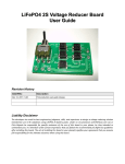
UM10437 GreenChip 65 W TEA1738LT/T and TEA1703 demo board Rev. 1 — 28 February 2011 User manual Document information Info Content Keywords Notebook adapter, TEA1738LT/T, TEA1703, fixed frequency, ultra-low standby power, high-efficiency, slim line Abstract This manual provides the specification, schematics and PCB layout of the 65 W TEA1738LT/T and TEA1703 demo board. For details on the TEA1738LT/T or TEA1703 IC please refer to the application note. UM10437 NXP Semiconductors GreenChip 65 W TEA1738LT/T and TEA1703 demo board Revision history Rev Date Description v.1 20110228 first issue Contact information For more information, please visit: http://www.nxp.com For sales office addresses, please send an email to: [email protected] UM10437 User manual All information provided in this document is subject to legal disclaimers. Rev. 1 — 28 February 2011 © NXP B.V. 2011. All rights reserved. 2 of 27 UM10437 NXP Semiconductors GreenChip 65 W TEA1738LT/T and TEA1703 demo board 1. Introduction WARNING Lethal voltage and fire ignition hazard The non-insulated high voltages that are present when operating this product, constitute a risk of electric shock, personal injury, death and/or ignition of fire. This product is intended for evaluation purposes only. It shall be operated in a designated test area by personnel qualified according to local requirements and labor laws to work with non-insulated mains voltages and high-voltage circuits. This product shall never be operated unattended. This 65 W TEA1738LT/T and TEA1703 demo board demonstrates the capabilities of the TEA1738LT/T Switched-Mode Power Supply (SMPS) controller and the TEA1703 standby controller. This manual provides the specification, schematics and PCB layout of the 65 W TEA1738LT/T and TEA1703 demo board. Refer to the TEA1738LT/T data sheet and application note (AN10981) for details on the TEA1738LT/T. In addition, refer to the TEA1703 datasheet and application note (AN11012) for details on the TEA1703. In Standby mode operation (no-load condition), the TEA1703 standby control IC monitors the output voltage and disables the primary controller until the output voltage has reached its lowest preset value. This ensures ultra-low standby power consumption. 019aab616 Fig 1. TEA1738LT/T and TEA1703 65 W demo board 1.1 Features • • • • • UM10437 User manual Universal mains supply operation OverCurrent Protection (OCP) OverPower Protection (OPP) Low ripple and noise Slim line transformer All information provided in this document is subject to legal disclaimers. Rev. 1 — 28 February 2011 © NXP B.V. 2011. All rights reserved. 3 of 27 UM10437 NXP Semiconductors GreenChip 65 W TEA1738LT/T and TEA1703 demo board • • • • • Low-cost implementation Indicator LED Ultra low no-load standby power (< 50 mW at 230 V, 50 Hz) ENERGY STAR compliant EMI CISPR22 compliant 2. Power supply specification Table 1. Input specification Symbol Description Conditions Specification Unit Vi input voltage - 90 to 264 V fi input frequency - 47 to 60 Hz Pi(no_load) input power (no-load) at 230 V; 50 Hz < 50 mW Table 2. Output specification Symbol Description Conditions Specification Unit Vo output voltage - 19 V Vo(min) Minimum output voltage during standby mode operation 12 V Vo(ripple)(p-p) peak-to-peak output ripple voltage 20 MHz bandwidth 200 mV Io output current continuous 0 to 3.34 A Io(p) peak output current for 50 ms 5 A Po output power 0 to 40 C 65 W tholdup hold-up time at 115 V; 60 Hz; full load 5 ms - line regulation - 1 % - load regulation - 2 % tstartup start-up time at 115 V; 60 Hz 3 s efficiency according to ENERGY STAR (EPS 2) 87 % - EMI CISPR22 compliant pass - 3. Performance data Performance figures based on the following PCB design: • Schematic version: Tuesday 18 November 2010 rev. A 3.1 Efficiency Efficiency measurements were made using an automated test program containing a temperature stability detection algorithm. The output voltage and current were measured using a 4-wire current sense configuration directly at the PCB connector. Measurements were performed for 115 V; 60 Hz and 230 V; 50 Hz. UM10437 User manual All information provided in this document is subject to legal disclaimers. Rev. 1 — 28 February 2011 © NXP B.V. 2011. All rights reserved. 4 of 27 UM10437 NXP Semiconductors GreenChip 65 W TEA1738LT/T and TEA1703 demo board Efficiency results[1][2] Table 3. Condition ENERGY Efficiency (%) STAR 2.0 Average 100 % 75 % efficiency load load requirement (%) 50 % load 100 % 1 W load 0.5 W 0.25 W 115 V, 60 Hz > 87 90.3 88.8 90.5 90.4 90.5 76.8 69.1 57.8 230 V, 50 Hz > 87 91.6 91.6 92.1 91.7 90.9 74.8 66.4 54.3 [1] Warm-up time: 10 minutes [2] There is an efficiency loss of 1 % (approximately) when measured at the end of a 1 m output cable. A DC current source V Cable 014aab147 Fig 2. DC resistance output cable DC resistance cable = voltage drop / current = 0.228 / 3.349 = 0.0681 (2-way). 3.2 No-load power consumption Power consumption performance of the total application board with no-load connected was measured using a Yokogawa WT210 digital power meter. Integration time was set to 6 minutes to calculate the average dissipated power. The output voltage variation results are shown in Table 4. Measurements were performed for 90 V; 60 Hz, 115 V; 60 Hz, 230 V; 50 Hz, and 264 V; 50 Hz. Table 4. Output voltage and power consumption: no-load Condition ENERGY STAR 2.0 requirement (mW) Output voltage high (V) Output voltage low (V) No-load power consumption (mW) 90 V; 60 Hz 300 19.8 14.2 8 115 V; 60 Hz 300 19.8 14.2 11 230 V; 50 Hz 300 19.8 14.2 39 264 V; 50 Hz 300 19.8 14.2 56 3.3 Minimum output current in normal operation The minimum current required to leave Standby mode and enter normal operation was measured for 90 V; 60 Hz and 264 V; 50 Hz. Table 5. UM10437 User manual Minimum current for normal operation Condition 90 V; 60 Hz 264 V; 50 Hz Current (mA) 2 5 All information provided in this document is subject to legal disclaimers. Rev. 1 — 28 February 2011 © NXP B.V. 2011. All rights reserved. 5 of 27 UM10437 NXP Semiconductors GreenChip 65 W TEA1738LT/T and TEA1703 demo board 3.4 Output regulation The output voltage as a function of load current was measured using a 4-wire current sense configuration directly at the PCB connector. Measurements were performed without probes attached to the application for 115 V; 60 Hz and 230 V; 50 Hz. 019aab617 20.0 Vo (V) 19.8 (1) (2) 19.6 19.4 19.2 19.0 0 1 2 3 4 Io (A) 5 (1) Vo = 115 V (AC); 60 Hz. (2) Vo = 230 V (AC); 50 Hz. Fig 3. Output voltage regulation as function of current load 3.5 Line regulation The output voltage as a function of mains input voltage was measured directly at the output connector for full load (3.34 A) condition. 019aab618 19.75 Vo (V) 19.65 19.55 19.45 19.35 19.25 Fig 4. UM10437 User manual 90 115 140 165 190 215 240 265 mains (Vac) Output voltage as function of mains voltage All information provided in this document is subject to legal disclaimers. Rev. 1 — 28 February 2011 © NXP B.V. 2011. All rights reserved. 6 of 27 UM10437 NXP Semiconductors GreenChip 65 W TEA1738LT/T and TEA1703 demo board 3.6 Output voltage regulation in Standby mode The output voltage regulation during no-load operation was measured for 90 V; 60 Hz and 264 V; 50 Hz. 019aab619 Chan1 (yellow): VCC; Chan2 (green): Gate pulse; Chan3 (magenta): VO Fig 5. Output voltage regulation at no-load 90 V; 60 Hz 019aab620 Chan1 (yellow): VCC; Chan2 (green): Gate pulse; Chan3 (magenta): VO Fig 6. UM10437 User manual Output voltage regulation at no-load 264 V; 50 Hz All information provided in this document is subject to legal disclaimers. Rev. 1 — 28 February 2011 © NXP B.V. 2011. All rights reserved. 7 of 27 UM10437 NXP Semiconductors GreenChip 65 W TEA1738LT/T and TEA1703 demo board 3.7 OverPower Protection (OPP) Nominal and peak output power was measured directly at the output connector for various mains input voltages. Peak output power was measured after removing C18 and replacing R16 for 180 k. 019aab621 150 Po (W) (2) 130 110 (1) 90 70 50 90 130 170 210 250 290 mains (Vac) (1) Nominal power (W). (2) Peak power (W). Fig 7. Nominal and peak output power as function of mains voltage 3.8 VCC voltage The IC VCC pin 1 voltage was measured for both no-load and full load (3.34 A) conditions. Table 6. VCC voltage Condition 115 V; 60 Hz 230 V; 50 Hz No-load 18.9 19.0 Full load (3.34 A) 21 20.2 3.9 Brownout and start level Brownout and start level was measured for no-load and full load (3.34 A) conditions. Table 7. Brownout and start level results Condition Brownout V (AC) Start level V (AC) No-load 63 84 Full load (3.34 A) 78 85 3.10 OverVoltage Protection (OVP) Applying a short-circuit across the opto-LED of the optocoupler (M5) creates an output overvoltage condition. The output voltage was measured directly at the output connector for both full load (3.34 A) and no-load condition. In no-load condition, the fault condition is processed when the primary controller is active. UM10437 User manual All information provided in this document is subject to legal disclaimers. Rev. 1 — 28 February 2011 © NXP B.V. 2011. All rights reserved. 8 of 27 UM10437 NXP Semiconductors GreenChip 65 W TEA1738LT/T and TEA1703 demo board Table 8. Maximum output voltage in case of OVP Condition 115 V (AC) 230 V (AC) No-load 25.6 25.6 Full load (3.34 A) 25 25.2 019aab622 Chan1 (yellow): VO; Chan2 (green): Gate pulse; Chan3 (magenta): Ctrl voltage. Fig 8. 230 V; 50 Hz; full load maximum output voltage when OVP is triggered 019aab623 Chan1 (yellow): VO; Chan2 (green): Gate pulse; Chan3 (magenta): Ctrl voltage. Fig 9. UM10437 User manual 230 V; 50 Hz; no-load maximum output voltage when OVP is triggered All information provided in this document is subject to legal disclaimers. Rev. 1 — 28 February 2011 © NXP B.V. 2011. All rights reserved. 9 of 27 UM10437 NXP Semiconductors GreenChip 65 W TEA1738LT/T and TEA1703 demo board 3.11 Start-up time Start-up time was measured for three mains input voltages and full load (3.34 A) condition. Vi input measured using a current probe (to avoid adding additional capacitance to the mains input). Vo was measured using a voltage probe grounded at the secondary side. Table 9. Start-up time Condition Start-up time (s) 90 V; 60 Hz 3.2 115 V; 60 Hz 2.0 230 V; 50 Hz 0.8 If the start-up time is considered too long, it is advised to change the input circuit as described in application note AN10981. 3.12 Start-up profile The shape of the output voltage was measured for three mains input voltages during start-up directly from the output connector under the full load (3.34 A) condition. Vo was measured using a voltage probe grounded at the secondary side. 019aab624 Chan1 (yellow): VO; Chan2 (green): Gate pulse; Chan3 (magenta): Ctrl voltage. Fig 10. 90 V; 60 Hz; full load; start up profile UM10437 User manual All information provided in this document is subject to legal disclaimers. Rev. 1 — 28 February 2011 © NXP B.V. 2011. All rights reserved. 10 of 27 UM10437 NXP Semiconductors GreenChip 65 W TEA1738LT/T and TEA1703 demo board 019aab625 Chan1 (yellow): VO; Chan2 (green): Gate pulse; Chan3 (magenta): Ctrl voltage. Fig 11. 264 V; 50 Hz; full load; start up profile Remark: The small discontinuity in the output voltage ramp at 264 V; 50 Hz is caused by the slow start function not limiting the primary current because it is hidden by the leading edge blanking period of 300 ns. 3.13 Hold-up time Hold-up time is defined as the time between the following moments: • After mains switch off; the moment that the lowest bulk cap voltage during a mains cycle is crossed • The moment that the output voltage starts to drop The hold-up time is measured for 115 V; 60 Hz under full load (3.34 A) condition. Output voltage duration was measured directly at the output connector. The hold-up time at 115 V, 60 Hz is 10.9 ms. UM10437 User manual All information provided in this document is subject to legal disclaimers. Rev. 1 — 28 February 2011 © NXP B.V. 2011. All rights reserved. 11 of 27 UM10437 NXP Semiconductors GreenChip 65 W TEA1738LT/T and TEA1703 demo board 019aab626 Chan1 (yellow): Vo; Chan3 (magenta): Bulk cap voltage. Fig 12. full load; hold–up time at 115 V; 60 Hz 3.14 Dynamic loading The output voltage was measured at the end of the cable. Both channels of the oscilloscope are set to DC mode. Table 10. UM10437 User manual Dynamic loading test conditions and results Condition Loading Vo(ripple)(p-p) (mV) 90 V; 47 Hz Io: 0 % to 50 %, frequency 50 Hz; duty cycle 50 % 375 264 V; 63 Hz Io: 0 % to 50 %, frequency 50 Hz; duty cycle 50 % 375 All information provided in this document is subject to legal disclaimers. Rev. 1 — 28 February 2011 © NXP B.V. 2011. All rights reserved. 12 of 27 UM10437 NXP Semiconductors GreenChip 65 W TEA1738LT/T and TEA1703 demo board 019aab627 Chan1 (yellow): Vo; Chan4 (cyan): Io. Fig 13. Dynamic loading 90 V; 47 Hz 019aab628 Chan1 (yellow): Vo; Chan4 (cyan): Io. Fig 14. Dynamic loading 264 V; 63 Hz UM10437 User manual All information provided in this document is subject to legal disclaimers. Rev. 1 — 28 February 2011 © NXP B.V. 2011. All rights reserved. 13 of 27 UM10437 NXP Semiconductors GreenChip 65 W TEA1738LT/T and TEA1703 demo board 3.15 Output ripple and noise Output ripple and noise were measured at the end of the cable using the measurement set-up described in Figure 15. An oscilloscope probe connected to the end of the adapter cable using a probe tip. 100 nF and 1 F capacitors were added between plus and minus to reduce the high frequency noise. Output ripple and noise were measured for mains voltages 90 V; 47 Hz and 264 V; 63 Hz, both at full load (3.34 A) output current. 1 μF Adapter cable 100 nF 1:10 Probe Probe tip 014aab151 Fig 15. Output ripple and noise measurement set-up Table 11. Output ripple and noise measurements Condition Vo(ripple)(p-p) (mV) 90 V; 47 Hz 130 264 V; 63 Hz 110 019aab629 Chan1 (yellow): Vo; Chan2 (green): Gate pulse Fig 16. Output ripple and noise at 90 V; 47 Hz UM10437 User manual All information provided in this document is subject to legal disclaimers. Rev. 1 — 28 February 2011 © NXP B.V. 2011. All rights reserved. 14 of 27 UM10437 NXP Semiconductors GreenChip 65 W TEA1738LT/T and TEA1703 demo board 019aab630 Chan1 (yellow): Vo; Chan2 (green): Gate pulse Fig 17. Output ripple and noise at 264 V; 63 Hz 3.16 EMI performance Conditions: • • • • • • Type: conducted EMC measurement Frequency range: 150 kHz to 30 MHz Output power: full load condition Supply voltage: 110 V and 230 V (AC) Margin: 6 dB below limit Measurements performed by Cerpass technology corp. Taipei (Taiwan) Remark: The displayed trace line in the following graphs is the quasi-peak measurement result UM10437 User manual All information provided in this document is subject to legal disclaimers. Rev. 1 — 28 February 2011 © NXP B.V. 2011. All rights reserved. 15 of 27 UM10437 NXP Semiconductors GreenChip 65 W TEA1738LT/T and TEA1703 demo board 019aab631 Fig 18. 115 V, 65 W TEA1738LT/T and TEA1703 demo board phase N 019aab632 Fig 19. 115 V, 65 W TEA1738LT/T and TEA1703 demo board phase L 019aab633 Fig 20. 230 V, 65 W TEA1738LT/T and TEA1703 demo board phase N UM10437 User manual 019aab634 Fig 21. 230 V, 65 W TEA1738LT/T and TEA1703 demo board phase L All information provided in this document is subject to legal disclaimers. Rev. 1 — 28 February 2011 © NXP B.V. 2011. All rights reserved. 16 of 27 xxxx xxxxxxxxxxxxxxxxxxxxxxxxxxxxxx x xxxxxxxxxxxxxx xxxxxxxxxx xxx xxxxxx xxxxxxxxxxxxxxxxxxxxxxx xxxxxxxxxxxxxxxxxxxxxx xxxxx xxxxxx xx xxxxxxxxxxxxxxxxxxxxxxxxxxxxx xxxxxxxxxxxxxxxxxxxxxx xxxxxxxxxxx xxxxxxx xxxxxxxxxxxxxxxxxxx xxxxxxxxxxxxxxxx xxxxxxxxxxxxxx xxxxxx xx xxxxxxxxxxxxxxxxxxxxxxxxxxxxxxxx xxxxxxxxxxxxxxxxxxxxxxxx xxxxxxx xxxxxxxxxxxxxxxxxxxxxxxxxxxxxxxxxxxxxxxxxxxxxx xxxxxxxxxxx xxxxx x x T1 1 R9 51 kΩ C3 F2 C1 0.33 μF L2 BD3 S2M BD4 S2M C2 110 μF 400 V R3 910 kΩ F 1 ZD2 BZX84J-B18 C6 0.22 μF 50 V R20 1 MΩ 2 F VISENSE M4-A KPS2801B 4 PROTECT 3 1 2 Q2 PMBT4401 3 R19 39 kΩ D4 1N4148w F F C17 0.1 μF 50 V C18 220 pF 50 V R30 330 kΩ 2 1 Q RT1 200 kΩ R17 8.06 kΩ F C10 22 nF 50 V F CTRL OPTIMER 4 C9 1 nF 50 V M53 KPS2801B F F C4 3300 pF 1 kV R5 10 MΩ R7 R6 10 MΩ 10 MΩ 4 6 7 D2 1N4148W M1 5 3 TEA1738T 8 2 1 DRIVER C29 68 pF 50 V GND VCC R16 2.2 MΩ C7 C8 0.1 μF 0.22 μF 50 V 50 V F F C31 SWDET R14 4.7 Ω 10 Ω R13 C28 1 kΩ 0.22 μF 50 V D3 BAV21 F R12 R11 0.2 Ω 33 kΩ F L3 6.8 μH F Fig 22. Schematic 65 W TEA1738LT/T and TEA1703 reference board 1 M3 M4-B R33 470 Ω LED 1 2 M5-B 1 R32 1 kΩ n.c. TEA1703 2 GND 3 R36 75 kΩ 1 R34 1 kΩ 2 2 6 D7 BAS21H C21 C12 220 pF 50 V n.c. L4 10 mH 1 nF 50 V R40 10 kΩ D9 1N4148W C20 R35 10 nF 50 V 10 kΩ M6 AS431I R37 11 kΩ D R38 330 kΩ 5 3 C11 3.3 μF 50 V 8 1 5 4 Q1 2SK3569 R15 7 C19 0.1 μF 50 V Q3 2N7002 G S PQ3220 F C22 0.1 μF 50 V R39 330 kΩ 019aab243 UM10437 17 of 27 © NXP B.V. 2011. All rights reserved. F R31 1.5 MΩ ISENSE F 1000 pF D1 SA2M n.c. R8 240 kΩ F ZD1 BZX84JB24 R28 240 kΩ VCC 3 R4 910 kΩ C16 56 pF 50 V C15 470 μF 25 V GND R2 910 kΩ N BD2 S2M Opto L5 BD1 S2M C14 470 μF 25 V GreenChip 65 W TEA1738LT/T and TEA1703 demo board Rev. 1 — 28 February 2011 All information provided in this document is subject to legal disclaimers. R1 910 kΩ R29 4.7 MΩ R27 330 kΩ 2200 pF 630 V 3.15 A 250 V D5 BAS21 VSENSE 1 FB PSENSE L 2 n.c. INLET R10 51 kΩ 19.5 V 3.34 A VOUT FA NXP Semiconductors D6 V40100C 4. Schematic 65 W TEA1738LT/T and TEA1703 reference board UM10437 User manual C13 220 pF 100 V R26 47 Ω UM10437 NXP Semiconductors GreenChip 65 W TEA1738LT/T and TEA1703 demo board 5. Bill of materials 5.1 Components list Table 12. Bill of materials Reference Value Description Package R1 910 k; 1 %; 4 W resistor; thin film chip SMD 1206 R2 910 k; 1 %; 4 W resistor; thin film chip SMD 1206 R3 910 k; 1 %; 4 W resistor; thin film chip SMD 1206 R4 910 k; 1 %; 4 W resistor; thin film chip SMD 1206 R5 10 M; 1 %; 4 W resistor; thin film chip SMD 1206 R6 10 M; 1 %; 4 W resistor; thin film chip SMD 1206 R7 10 M; 1 %; 4 W resistor; thin film chip SMD 1206 R8 240 k; 5 %; 8 W resistor; thin film chip SMD 0805 R9 51 k; 1 %; 1 W resistor; thin film chip SMD 1206 R10 51 k; 1 %; 1 W resistor; thin film chip SMD 1206 R11 0.2 ; 1 %; 1 W resistor; MOF axial lead R12 33 k; 1 %; 10 W resistor; thin film chip SMD 0603 R13 1 k; 1 %; 1 W resistor; thin film chip SMD 0603 R14 10 ; 5 %; 8 W resistor; thin film chip SMD 0603 R15 4.7 ; 5 %; 8 W resistor; thin film chip SMD 0805 R16 2.2 M; 5 %; 10 W resistor; thin film chip SMD 0603 R17 8.06 k; 5 %; 10 W resistor; thin film chip SMD 0603 R19 39 k; 5 %; 10 W resistor; thin film chip SMD 0603 R20 1 M; 5 %; 10 W resistor; thin film chip SMD 0603 R26 4.7 ; 5 %; 8 W resistor; thin film chip SMD 0603 R27 330 k; 5 %; 10 W resistor; thin film chip SMD 0603 R28 240 k; 5 %; 10 W resistor; thin film chip SMD 0603 R29 4.7 M; 5 %; 10 W resistor; thin film chip SMD 0603 R30 330 k; 5 %; 10 W resistor; thin film chip SMD 0603 R31 1.5 M; 5 %; 10 W resistor; thin film chip SMD 0603 R32 - not mounted - R33 470 ; 5 %; 8 W resistor; thin film chip SMD 0603 R34 1 k; 5 %; 10 W resistor; thin film chip SMD 0603 R35 10 k; 5 %; 10 W resistor; thin film chip SMD 0603 R36 75 k; 5 %; 10 W resistor; thin film chip SMD 0603 R37 11 k; 5 %; 10 W resistor; thin film chip SMD 0603 R38 330 k; 5 %; 10 W resistor; thin film chip SMD 0603 R39 330 k; 5 %; 10 W resistor; thin film chip SMD 0603 R40 10 k; 5 %; 10 W resistor; thin film chip SMD 0603 RT1 200 k; 5 % NTC resistor SMD 0805 C1 330 F; 400 V; 105 C X2-cap; Arcotronics 15 mm 14.5 mm 8.5 mm C2 110 F; 400 V; 105 C electric; 20 %, NCC 50 mm 11.5 mm UM10437 User manual All information provided in this document is subject to legal disclaimers. Rev. 1 — 28 February 2011 © NXP B.V. 2011. All rights reserved. 18 of 27 UM10437 NXP Semiconductors GreenChip 65 W TEA1738LT/T and TEA1703 demo board Table 12. Bill of materials …continued Reference Value Description Package C3 2200 pF; 630 V MLCC; Z5U SMD 1206 C4 3300 pF; 1 kV MLCC; Z5U SMD 1206 C6 0.22 F; 50 V 10 %; MLCC; X7R; lead free SMD 0603 C7 0.1 F; 50 V 10 %; MLCC; X7R SMD 0603 C8 0.22 F; 50 V 10 %; MLCC; X7R; lead free SMD 0603 C9 1 nF; 50 V 10 %; MLCC; X7R SMD 0603 C10 22 nF; 50 V 5 %; MLCC; X7R SMD 0603 C11 3.3 F; 50 V; 105 C electric, 20 %; KY/NCC 5 mm 11.5 mm C12 - not mounted - C13 220 pF; 100 V 5 %; MLCC; NPO; KZH/NCC SMD 0805 C14 470 F; 50 V; 105 C electric, 20 %; KZH/NCC radial lead; 10 mm 12.5 mm C15 470 F; 50 V; 105 C electric, 20 %; KZH/NCC radial lead; 10 mm 12.5 mm C16 56 pF; 50 V 5 %; MLCC; X7R SMD 0603 C17 0.1 F; 50 V 10 %; MLCC; X7R SMD 0603 C18 220 pF; 50 V 5 %; MLCC; X7R SMD 0603 C19 0.1 F; 50 V 10 %; MLCC; X7R SMD 0603 C20 10 nF; 50 V 10 %; MLCC; X7R SMD 0603 C21 1 nF; 50 V 10 %; MLCC; X7R SMD 0603 C22 0.1 nF; 50 V 10 %; MLCC; X7R SMD 0603 C28 0.22 nF; 50 V 10 %; MLCC; X7R; lead free SMD 0603 C31 1000 pF; 400 V (AC) Y1-cap - BD1 2 A; 1 kV general purpose diode; S2M; trr = 2 S; MCCsemi SMB BD2 2 A; 1 kV general purpose diode; S2M; trr = 2 S; MCCsemi SMB BD3 2 A; 1 kV general purpose diode; S2M; trr = 2 S; MCCsemi SMB BD4 2 A; 1 kV general purpose diode; S2M; trr = 2 S; MCCsemi SMB D1 2 A; 1 kV general purpose diode; S2M; trr = 2 S; MCCsemi SMT SMB D2 0.15 A; 100 V switching diode; 1N4148W; trr = 4 nS SMT SOD123 D3 0.2 A; 250 V diode; BAV21W/Vishay; trr = 50 nS SMT SOD123 D4 0.15 A; 100 V switching diode; 1N4148W; trr = 4 nS SMT SOD123 D5 0.2 A; 250 V diode; BAV21W/Vishay; trr = 50 nS SMT SOD123 D6 40 A; 100 V Schottky; V40100C; Vishay TO220AB D7 0.2 A; 250 V diode; BAV21H/Vishay; trr = 50 nS; NXP SMT SOD123 D8 0.15 A; 100 V switching diode; 1N4148W; trr = 4 nS SMT SOD123 D9 0.15 A; 100 V switching diode; 1N4148W; trr = 4 nS SMT SOD123 ZD1 24 V Zener diode; BZX84J-B24; Vz = 23.5 V to 24.5 V; zt = 5 mA; Ir = 50 nA SMT SOD323F ZD2 24 V Zener diode; BZX84J-B18; Vz = 17.6 V to 18.4 V; zt = 5 mA; Ir = 50 nA SMT SOD323F UM10437 User manual All information provided in this document is subject to legal disclaimers. Rev. 1 — 28 February 2011 © NXP B.V. 2011. All rights reserved. 19 of 27 UM10437 NXP Semiconductors GreenChip 65 W TEA1738LT/T and TEA1703 demo board Table 12. Bill of materials …continued Reference Value Description Package ZD3 - not mounted - Q1 15 A; 600 V; 0.5 MOSFET; n-channel; 2SK3569/Toshiba; RDSon = 0.5 ; VGS(on) = 3 V; ID = 15 A; Ciss = 1600 pF; VDS = 600 V; VGS = 30 V SMT TO220 Q2 PMBT4401 NPN transistor 80 hFE; VCEO = 40 V; IC = 600 mA SMT TO220 Q3 15 A; 600 V; 0.5 MOSFET; n-channel; 2SK3569/Toshiba; RDSon = 5.3 ; VGS(on) = 1 V; ID = 300 mA; Ciss = 40 pF; VDS = 60 V; VGS = 30 V SMT SOT23 M1 TEA1738LT/T GreenChip SMPS control IC; NXP Semiconductors SO8 M3 TEA1703 GreenChip SMPS control IC; NXP Semiconductors SO8 M4 KPS2801B optocoupler; CTR = 130 % ~ 260 %; 1-channel; COSMO 4-pin SOP M5 KPS2801B optocoupler; CTR = 130 % ~ 260 %; 1-channel; COSMO 4-pin SOP M6 AS431l adjustable precision shunt regulator BCD SMT SOT23 T1 Lp = 400 H transformer; Np : Ns : Naux = 36 : 6 : 6; JPP44A; A-core ATQ28/11.2D L2 choke N1 : N2 = 52 : 52; JPH10F; A-core D = 0.45 mm; 14 mm 59C L3 6.8 H choke; 10 %; 275 A; DCR = 1 ; WIS252018N-6R8K; Mingstar SMT 2.5 mm 2 mm 1.8 mm L4 10 H choke DIP L5 choke N1 : N2 = 7 : 7; JPZ10K; A-core D = 0.45 mm; T8 mm 4 mm 49C F2 T3.15 A; 250 V fuse; f7use; DIP; MST 8.35 mm 4.3 mm 7.7 mm LED1 LED 5.0 V; blue M02-0603QBC; Vr = 5 V; IF = 30 mA; Hi-light SMD 0603; 1.6 mm 0.8 mm 0.8 mm Inlet inlet - 2P Cable cable 16AWG/1571 L = 1200 mm UM10437 User manual All information provided in this document is subject to legal disclaimers. Rev. 1 — 28 February 2011 © NXP B.V. 2011. All rights reserved. 20 of 27 UM10437 NXP Semiconductors GreenChip 65 W TEA1738LT/T and TEA1703 demo board 6. Transformer specification 6.1 Transformer schematic diagram 2 N3 FLYA A N1, N6, N9 N8 FLYB 1 5 N4 3 N2, N5, N7 PRIMARY winding start SECONDARY teflon tube copper foil 019aab248 Fig 23. Transformer winding diagram Table 13. UM10437 User manual Winding construction Number Layers Turns Wires Copper/diameter Type 9 secondary 6 2 0.32 triso 8c primary 6 1 0.35 enamelled 8b primary 6 1 0.35 enamelled 8a primary 6 1 0.35 enamelled 7 Cu foil - - - - 6 secondary 6 2 0.35 triso 5 Cu foil - - - - 4 auxiliary 6 2 0.32 enamelled 3c primary 6 1 0.15 enamelled 3b primary 6 1 0.35 enamelled 3a primary 6 1 0.35 enamelled 2 Cu foil - - - - 1 secondary 6 2 0.32 triso All information provided in this document is subject to legal disclaimers. Rev. 1 — 28 February 2011 © NXP B.V. 2011. All rights reserved. 21 of 27 UM10437 NXP Semiconductors GreenChip 65 W TEA1738LT/T and TEA1703 demo board 6.2 Winding specification Table 14. Winding table Winding order Pin Start Finish 1 N1 FA 2 S1 3 N3 Wire Turns Layers Turn/ Insulation after Layer winding FB 0.32 mm 2 mm[1] 6 1 6 tape 1 Ts[3] - 3[6] 0.025 mm 7 mm[2] 1 1 1 tape 1 Ts[3] 2 A 0.35 mm 2 mm 18 3 6/3 tape 1 Ts[3] 0.15 mm 2 mm 6 1 6 tape 1 Ts[3][5] 4 N4 5 3[6] 5 S2 - 3 0.025 mm 7 mm[2] 1 1 1 tape 1 Ts[3] 6 N6 FA FB 0.32 mm 2 mm[1] 6 1 6 tape 1 Ts[3] 7 S3 - 3[6] 0.025 mm 7 mm[2] 1 1 1 tape 1 Ts[3] 8 N8 A[4] 1 0.35 mm 2 mm 18 3 6/3 tape 1 Ts[3] 9 N9 FA FB 0.3 mm 2 mm[1] 6 1 6 tape 1 Ts[3] [1] Furkukawa. [2] Copper foil. [3] Spread winding. [4] Intermediate connection A is not connected to a pin. [5] Insulation tape 3M #1350 or #1298. [6] Copper foil connected to pin 3 using 0.25 lead wire. 6.3 Electrical characteristics Table 15. Electrical characteristics Description Pin Specification Remark Inductance 1 to 2 700 H ± 5 % 65 kHz; 1 V 6.4 Core and bobbin Core: ATQ28/11.2D; A-Core, JPP44A 6.5 Marking Main board: APBADC054 UM10437 User manual All information provided in this document is subject to legal disclaimers. Rev. 1 — 28 February 2011 © NXP B.V. 2011. All rights reserved. 22 of 27 UM10437 NXP Semiconductors GreenChip 65 W TEA1738LT/T and TEA1703 demo board 7. Layout of the 65 W TEA1738LT/T and TEA1703 reference board 019aab245 Fig 24. Copper layout bottom side (top view) 019aab247 Fig 25. Copper layout top side (top view) UM10437 User manual All information provided in this document is subject to legal disclaimers. Rev. 1 — 28 February 2011 © NXP B.V. 2011. All rights reserved. 23 of 27 UM10437 NXP Semiconductors GreenChip 65 W TEA1738LT/T and TEA1703 demo board 019aab244 Fig 26. Component placement bottom side (bottom view) 019aab246 Fig 27. Component placement top side (top view) UM10437 User manual All information provided in this document is subject to legal disclaimers. Rev. 1 — 28 February 2011 © NXP B.V. 2011. All rights reserved. 24 of 27 UM10437 NXP Semiconductors GreenChip 65 W TEA1738LT/T and TEA1703 demo board 8. Alternative circuit options 8.1 Changing the output voltage By changing the following components, the output voltage can be changed (30 %). Refer to the TEA1738(L)T application note for additional information on this topic. Make sure that the Aux voltage remains within its operation limits (12.2 V 30 V typical) and is high enough to start up (20.6 V typical). R23/R24 The resistor divider R36 and R37 determine the output voltage based on Vo = 2.5 V (R36 + R37) / (R37). C13/C14 The voltage rating of these electrolytic capacitors must be chosen to be higher than the output voltage. Decrease the value of the capacitors for applications with a lower output current. 8.2 TEA1703 adjustments In this design the following items can be improved by changing the value of the inductor L4 to 4m7H. Currently the current through opto LED M4 is too low. • Output power level threshold to enter Standby mode is very low • The VCC clamp cannot sink enough current for high mains. This causes the TEA1738 to restart in Standby mode at 264 V; 60 Hz. This behavior is not recommended The minimum output voltage in Standby mode can be adjusted using resistor R30. By increasing resistor R30 from 330 k to 420 k, an additional < 2 mW can be saved and the minimum output voltage will drop to 9 V. Refer to the TEA1703 application note for adjustment information. UM10437 User manual All information provided in this document is subject to legal disclaimers. Rev. 1 — 28 February 2011 © NXP B.V. 2011. All rights reserved. 25 of 27 UM10437 NXP Semiconductors GreenChip 65 W TEA1738LT/T and TEA1703 demo board 9. Legal information 9.1 Definitions Draft — The document is a draft version only. The content is still under internal review and subject to formal approval, which may result in modifications or additions. NXP Semiconductors does not give any representations or warranties as to the accuracy or completeness of information included herein and shall have no liability for the consequences of use of such information. 9.2 Disclaimers Limited warranty and liability — Information in this document is believed to be accurate and reliable. However, NXP Semiconductors does not give any representations or warranties, expressed or implied, as to the accuracy or completeness of such information and shall have no liability for the consequences of use of such information. In no event shall NXP Semiconductors be liable for any indirect, incidental, punitive, special or consequential damages (including - without limitation - lost profits, lost savings, business interruption, costs related to the removal or replacement of any products or rework charges) whether or not such damages are based on tort (including negligence), warranty, breach of contract or any other legal theory. Notwithstanding any damages that customer might incur for any reason whatsoever, NXP Semiconductors’ aggregate and cumulative liability towards customer for the products described herein shall be limited in accordance with the Terms and conditions of commercial sale of NXP Semiconductors. Right to make changes — NXP Semiconductors reserves the right to make changes to information published in this document, including without limitation specifications and product descriptions, at any time and without notice. This document supersedes and replaces all information supplied prior to the publication hereof. Suitability for use — NXP Semiconductors products are not designed, authorized or warranted to be suitable for use in life support, life-critical or safety-critical systems or equipment, nor in applications where failure or malfunction of an NXP Semiconductors product can reasonably be expected to result in personal injury, death or severe property or environmental damage. NXP Semiconductors accepts no liability for inclusion and/or use of NXP Semiconductors products in such equipment or applications and therefore such inclusion and/or use is at the customer’s own risk. Applications — Applications that are described herein for any of these products are for illustrative purposes only. NXP Semiconductors makes no representation or warranty that such applications will be suitable for the specified use without further testing or modification. Customers are responsible for the design and operation of their applications and products using NXP Semiconductors products, and NXP Semiconductors accepts no liability for any assistance with applications or customer product UM10437 User manual design. It is customer’s sole responsibility to determine whether the NXP Semiconductors product is suitable and fit for the customer’s applications and products planned, as well as for the planned application and use of customer’s third party customer(s). Customers should provide appropriate design and operating safeguards to minimize the risks associated with their applications and products. NXP Semiconductors does not accept any liability related to any default, damage, costs or problem which is based on any weakness or default in the customer’s applications or products, or the application or use by customer’s third party customer(s). Customer is responsible for doing all necessary testing for the customer’s applications and products using NXP Semiconductors products in order to avoid a default of the applications and the products or of the application or use by customer’s third party customer(s). NXP does not accept any liability in this respect. Export control — This document as well as the item(s) described herein may be subject to export control regulations. Export might require a prior authorization from national authorities. Evaluation products — This product is provided on an “as is” and “with all faults” basis for evaluation purposes only. NXP Semiconductors, its affiliates and their suppliers expressly disclaim all warranties, whether express, implied or statutory, including but not limited to the implied warranties of non-infringement, merchantability and fitness for a particular purpose. The entire risk as to the quality, or arising out of the use or performance, of this product remains with customer. In no event shall NXP Semiconductors, its affiliates or their suppliers be liable to customer for any special, indirect, consequential, punitive or incidental damages (including without limitation damages for loss of business, business interruption, loss of use, loss of data or information, and the like) arising out the use of or inability to use the product, whether or not based on tort (including negligence), strict liability, breach of contract, breach of warranty or any other theory, even if advised of the possibility of such damages. Notwithstanding any damages that customer might incur for any reason whatsoever (including without limitation, all damages referenced above and all direct or general damages), the entire liability of NXP Semiconductors, its affiliates and their suppliers and customer’s exclusive remedy for all of the foregoing shall be limited to actual damages incurred by customer based on reasonable reliance up to the greater of the amount actually paid by customer for the product or five dollars (US$5.00). The foregoing limitations, exclusions and disclaimers shall apply to the maximum extent permitted by applicable law, even if any remedy fails of its essential purpose. 9.3 Trademarks Notice: All referenced brands, product names, service names and trademarks are the property of their respective owners. GreenChip — is a trademark of NXP B.V. All information provided in this document is subject to legal disclaimers. Rev. 1 — 28 February 2011 © NXP B.V. 2011. All rights reserved. 26 of 27 UM10437 NXP Semiconductors GreenChip 65 W TEA1738LT/T and TEA1703 demo board 10. Contents 1 1.1 2 3 3.1 3.2 3.3 3.4 3.5 3.6 3.7 3.8 3.9 3.10 3.11 3.12 3.13 3.14 3.15 3.16 4 5 5.1 6 6.1 6.2 6.3 6.4 6.5 7 8 8.1 8.2 9 9.1 9.2 9.3 10 Introduction . . . . . . . . . . . . . . . . . . . . . . . . . . . . 3 Features . . . . . . . . . . . . . . . . . . . . . . . . . . . . . . 3 Power supply specification. . . . . . . . . . . . . . . . 4 Performance data. . . . . . . . . . . . . . . . . . . . . . . . 4 Efficiency . . . . . . . . . . . . . . . . . . . . . . . . . . . . . 4 No-load power consumption . . . . . . . . . . . . . . . 5 Minimum output current in normal operation . . 5 Output regulation . . . . . . . . . . . . . . . . . . . . . . . 6 Line regulation . . . . . . . . . . . . . . . . . . . . . . . . . 6 Output voltage regulation in Standby mode . . . 7 OverPower Protection (OPP) . . . . . . . . . . . . . . 8 VCC voltage . . . . . . . . . . . . . . . . . . . . . . . . . . . 8 Brownout and start level . . . . . . . . . . . . . . . . . . 8 OverVoltage Protection (OVP) . . . . . . . . . . . . . 8 Start-up time . . . . . . . . . . . . . . . . . . . . . . . . . . 10 Start-up profile . . . . . . . . . . . . . . . . . . . . . . . . 10 Hold-up time . . . . . . . . . . . . . . . . . . . . . . . . . . 11 Dynamic loading . . . . . . . . . . . . . . . . . . . . . . . 12 Output ripple and noise . . . . . . . . . . . . . . . . . 14 EMI performance . . . . . . . . . . . . . . . . . . . . . . 15 Schematic 65 W TEA1738LT/T and TEA1703 reference board . . . . . . . . . . . . . . . . . . . . . . . . 17 Bill of materials . . . . . . . . . . . . . . . . . . . . . . . . 18 Components list . . . . . . . . . . . . . . . . . . . . . . . 18 Transformer specification . . . . . . . . . . . . . . . . 21 Transformer schematic diagram . . . . . . . . . . . 21 Winding specification . . . . . . . . . . . . . . . . . . . 22 Electrical characteristics . . . . . . . . . . . . . . . . . 22 Core and bobbin . . . . . . . . . . . . . . . . . . . . . . . 22 Marking . . . . . . . . . . . . . . . . . . . . . . . . . . . . . . 22 Layout of the 65 W TEA1738LT/T and TEA1703 reference board . . . . . . . . . . . . . . . . . . . . . . . . 23 Alternative circuit options. . . . . . . . . . . . . . . . 25 Changing the output voltage. . . . . . . . . . . . . . 25 TEA1703 adjustments . . . . . . . . . . . . . . . . . . 25 Legal information. . . . . . . . . . . . . . . . . . . . . . . 26 Definitions . . . . . . . . . . . . . . . . . . . . . . . . . . . . 26 Disclaimers . . . . . . . . . . . . . . . . . . . . . . . . . . . 26 Trademarks. . . . . . . . . . . . . . . . . . . . . . . . . . . 26 Contents . . . . . . . . . . . . . . . . . . . . . . . . . . . . . . 27 Please be aware that important notices concerning this document and the product(s) described herein, have been included in section ‘Legal information’. © NXP B.V. 2011. All rights reserved. For more information, please visit: http://www.nxp.com For sales office addresses, please send an email to: [email protected] Date of release: 28 February 2011 Document identifier: UM10437