1
picoFlash
User’s Manual
picoFlash User’s Manual
JK microsystems
Unless otherwise noted, this document and the information herein disclosed are proprietary to
JK microsystems, Inc. Any person or entity to whom this document is furnished or having
possession thereof, by acceptance, assumes custody thereof and agrees that the document is given
in confidence and will not be copied or reproduced in whole or in part to meet the purposes for
which it was delivered.
The information in this document is subject to change without notice, and should not be
construed as a commitment by JK microsystems, Inc. JK microsystems, Inc. will make every
effort to inform users of substantive errors.
JK microsystems, Inc. disclaims all liability for any loss or damage resulting from the use of this
manual or any software described herein, including without limitation contingent, special, or
incidental liability.
JK microsystems, Inc. recognizes our customer’s need for a consistent product and will make
every effort to provide one. In order to provide the best possible product for all of our customers,
we reserve the right to make incremental improvements in our product designs.
picoFlash is a trademark of JK microsystems, Inc. MS-DOS is a registered trademark of
Microsoft Corporation. XDOS is a copyright of HBS Corporation. All other brand and product
names are trademarks or registered trademarks of their respective companies.
picoFlash User’s Manual Version 1.1
Copyright © JK microsystems, Inc.
All rights reserved
Printed in U.S.A.
Document Part No. 94-0030
Published February 2004
i
JK microsystems
picoFlash User’s Manual
Limited Warranty
JK microsystems, Inc. warrants each picoFlash to be free from defects in material and
workmanship for a period of 90 days from the date of purchase. This warranty shall not apply to
any unit which has been subject to misuse, neglect, accident, or abnormal conditions of
operation.
JK microsystems’ obligation under this warranty is limited to repairing or replacing, at
JK microsystems’ option, any unit returned to the factory within 90 days of the date of purchase,
provided that JK microsystems determines that the unit is defective and has been used in
compliance with the terms of this warranty. If the failure has been caused by misuse, neglect,
accident, or abnormal conditions of operation, repairs will be billed at a nominal cost.
The foregoing warranty is exclusive and in lieu of all other warranties, expressed or implied,
including, but not limited to, any warranty of merchantability or fitness for any particular
purpose. JK microsystems shall not be liable for any special, incidental or consequential
damages, whether in contract, tort, or otherwise.
Important Notice
Life Support / Mission Critical Applications
This product is not fault-tolerant and is not designed, manufactured or intended for use or resale
as on-line control equipment in hazardous environments requiring fail-safe performance, such as
in the operation of nuclear facilities, aircraft navigation or communication systems, air traffic
control, direct life support machines, or weapons systems, in which the failure of our hardware or
software could lead directly to death, personal injury, or severe physical or environmental
damage.
ii
Limited Warranty
picoFlash User’s Manual
JK microsystems
Table of Contents
Limited Warranty ............................................................................................................................ ii
Table of Contents ........................................................................................................................... iii
Overview ........................................................................................................................................ 1
Features ........................................................................................................................................... 1
Operation ........................................................................................................................................ 2
Getting Started ................................................................................................................................ 3
Hardware ........................................................................................................................................ 5
Memory Configuration ............................................................................................................. 5
I/O Configuration...................................................................................................................... 5
Digital I/O Ports ........................................................................................................................ 5
Table 1: Memory Map Configuration Register ................................................................... 5
Driving Loads with the I/O Ports .............................................................................................. 6
Table 2: I/O Configuration Register ................................................................................... 6
Programming the I/O Ports ....................................................................................................... 7
Asynchronous Serial Ports ........................................................................................................ 8
RS-485 Configuration............................................................................................................... 8
Console Serial Port ................................................................................................................... 9
Watchdog Timer ....................................................................................................................... 9
Ethernet ................................................................................................................................... 10
Table 3: Watchdog timeout configuration ........................................................................ 11
DiskOnChip ............................................................................................................................ 11
Jumpers ................................................................................................................................... 11
JP1 - Serial Port 0 Select, RS-485 Termination................................................................ 11
JP2 - Socket Memory Type / Boot Memory Location ...................................................... 12
Cables and Connectors ........................................................................................................... 12
Table 4a: Power Pinout ..................................................................................................... 13
Table 4d: Serial 0 Pinout .................................................................................................. 13
Table 4b: Port A&B Pinout............................................................................................... 13
Table 4e: Serial 1 Pinout ................................................................................................... 13
Table 4c: Debug & PortC Pinout ...................................................................................... 13
Table 4h: Ethernet Pinout ................................................................................................. 13
Table 4f: JTAG & Port D Pinout ...................................................................................... 13
Table 4g: RS-485 Pinout ................................................................................................... 13
Software ........................................................................................................................................ 14
Supported PC BIOS Functions ............................................................................................... 14
Driver Library ......................................................................................................................... 14
Programming Languages ........................................................................................................ 14
QuickBASIC/PowerBASIC Console I/O ............................................................................... 15
Utilities ......................................................................................................................................... 16
UP.COM ................................................................................................................................. 16
DOWN.COM.......................................................................................................................... 16
FORMAT.COM ...................................................................................................................... 17
EDIT.COM ............................................................................................................................. 17
Table of Contents
iii
JK microsystems
picoFlash User’s Manual
DOS .............................................................................................................................................. 18
XDOS Command Reference .................................................................................................. 18
Specifications................................................................................................................................ 21
Contact Information ...................................................................................................................... 22
iv
JK microsystems
picoFlash User’s Manual
Overview
The picoFlash single board computer is based on the RDC R8822 microcomputer. The R8822 is
a high performance, 16-bit, single-chip microcomputer that is software compatible with the
80C186 family of microprocessors. DOS compatibility allows development in a familiar
environment with a wide range of tools. High endurance flash memory eliminates EPROM
programming without worry of damaging the onboard non-volatile memory with repeated
program cycles. Applications are uploaded directly into the flash disk. Expansion options provide
high capacity flash storage eliminating the size and reliability problems associated with electromechanical storage devices.
Software development for the picoFlash is remarkably simple and quick. Programs are written on
a PC compatible computer in the language of your choice. After your application has been
compiled or assembled and linked into .EXE or .COM form, it is uploaded to the picoFlash’s
flash disk with your favorite telecommunications program using the X-Modem protocol. The
application can then be tested and debugged through the serial console. When the application is
running to your satisfaction, the startup batch file can be modified so that the application will
load and execute upon reset or powerup.
Features
40MHz RDC R8822 Processor (x186 Compatible)
5V regulated DC power
512k Bytes DRAM Memory (16 bit data path)
512k Bytes Flash Memory
10 BASE-T Ethernet, NE2000 Compatible
High Speed Serial Ports (2):
115200 baud with RS-232 output levels
1 RS-232 Port with Handshake (TxD, RxD, DCD, RTS, CTS, GND)
Jumper Configurable as RS-232, TTL RS-232 or RS-485
1 RS-232 Port (3 wire)
Debug Serial Port (3 wire RS-232, 9600 baud console only)
16 Digital I/O Lines
Hardware Clock/Calendar
2 - 16 bit timer channels
Watchdog timer (generates internal processor reset)
32Pin Dip Socket to accept M-Systems DiskOnChip.
Compact Size, 3.75" x 2.5" (95mm x 63.5mm), 1.8oz (51gm)
Driver Library (C and Basic) - Serial ports, PIO, and alpha-numeric LCD
Overview
1
JK microsystems
picoFlash User’s Manual
Operation
The picoFlash is configured with two ‘disk drives’ A: and B:. Drive A: contains DOS, the BIOS,
and utility programs essential to the operation of the picoFlash. Drive A: is read-only. Drive B: is
read/write and contains optional utility programs and is available for user files and applications.
The default serial console port for the picoFlash is the Serial 1 port on the R8822, wired to J5.
The port is configured for 9600 baud, 8 data bits, 1 stop bit and no parity. This is the primary
mode of communicating with the picoFlash. DOS and the BIOS treat this port as the logical
devices STDIN and STDOUT, in place of a keyboard and monitor. The console can be relocated
to Serial 0 or the Debug port (freeing up both hardware serial ports). When the console is located
on a hardware serial port, the default baudrate can be also be changed. Configuring the console
port is described later in this manual.
When power is applied to the picoFlash or when it is reset, the board goes through its
initialization procedure and then starts DOS. A simple (read-only) AUTOEXEC.BAT file is executed
and then the board is ready to use. The batch file performs several functions before the user is
given control. The DOS search path is set, the DOS prompt is set, the CNTL-C flag (discussed
later in this manual) is checked and finally, an attempt is made to execute a file named
STARTUP on the B: drive. This provides a convenient way for user applications to execute
immediately after initialization of the picoFlash. If you wish to have your application start
automatically, create a batch file named STARTUP.BAT that invokes the program. Renaming your
application STARTUP.EXE or STARTUP.COM is not recommended. If this is done and the program
locks up, typing CNTL-C at bootup may not break the program and exit to the DOS prompt.
!
!
2
Although the flash memory devices used have a guaranteed lifetime of over 10,000 write
cycles, it is possible for an application to quickly wear them out. The flash memory is
intended to store programs, and setup data which is normally not changed. Avoid storing
data or frequently changed information on the flash disk.
To reduce the possibility of an unexpected powerdown corrupting the flash disk, it is
strongly recommended that flash file writes be done as quickly as possible. After the file
write, close the file and issue a Disk Reset, Int 21h function 0Dh. For more information,
see the Application Note on Flash Disk Reliability,
http://www.jkmicro.com/documentation#app_notes
Operation
JK microsystems
picoFlash User’s Manual
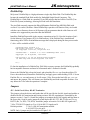
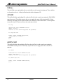
Getting Started
To begin development with the picoFlash, you will need a PC compatible computer with a
telecommunications program and a free serial port. Connect the picoFlash’s Debug/Console Port
to the PC’s serial port with a 9-pin serial cable (straight through wiring). Run the
telecommunications program and configure the serial port for 9600 baud, 8 data bits, 1 stop bit
and no parity. A tutorial for hyperterminal users is available on the DevKit CD and from the
documentation page of our website. Apply power to the picoFlash, using our A/C adapter
PN 88-0004 or a source of regulated 5 volt DC, capable of supplying 2 Watts. Observe the
polarity indicated on the board silkscreen.
DS1
ETHERNET
GND
RESET/
+5V
LNK
ACT
CONSOLE
The picoFlash should respond with a welcome message and a B: prompt. Enter DIR to look at the
directory of drive B:. If you do not get a welcome message or echo of the characters that you
type, you need to check your serial port setup. To test everything but the picoFlash, remove the
serial cable from J5 and short pins 3 and 5. If characters sent to the picoFlash are not echoed, the
problem is with your setup. You must resolve the problem before you can continue.
If you were able to do a DIR, take a few minutes to explore the contents of the picoFlash’s file
system. You will find all of the essential utilities on drive A: and some optional programs on
drive B:. Drive A: is write-protected and cannot be altered. Drive B: is read/write and can be
changed or reformatted.
After you have looked at the programs on the picoFlash, the next step is to try to upload a file.
This is the procedure for getting a file from your PC to the picoFlash. On the picoFlash, type the
command UP followed by the name of the file you wish to upload. The picoFlash will begin
sending characters to your PC polling it for the file.
On your PC, start the transfer, usually by pressing the PgUp key. The telecomm program should
respond by requesting the file name and protocol. Enter the file name and select X-Modem for
the protocol. The transfer should start and when it is complete, you should get a new B: prompt
Getting Started
3
JK microsystems
picoFlash User’s Manual
on the screen. If the transfer does not work, there are two things to check. First, verify that the
terminal program does not have handshaking or flow control enabled. Second, the Carrier Detect
signal (pin 1 on the DB-9 connector) into the PC could be sensed as low or false. Make sure that
the signal is at least +3 volts into your PC if you are not able to transfer files.
If the transfer terminated without problems, you have a working development environment for
the picoFlash controller. To transfer files from the picoFlash to the development PC, use the DOWN
command described in the Utilities section of this manual.
Depending on your application, all of the files on the B: drive are optional. The only file, in
addition to your application and STARTUP.BAT, that may be needed in a production environment
is the ethernet packet driver. All of the remaining files are pre-loaded in the hope that they will be
useful development tools. The files present on the B: drive are archived on the development CD
in the \JKmicro\picoFlash\Drive_B_Files\ directory.
The picoFlash has a hardware clock calendar. The time and date can be set from the DOS prompt
with the following commands:
B:\>TIME 13:30:00
B:\>DATE 11-29-2003
Sets the time to 1:30 pm
Sets the date to November 29, 2003
When power is applied to the picoFlash, one of the first things the BIOS initialization code does
is check for a CNTL-C character received by either the Console serial port or the Debug serial
port. If this character is typed as soon as the board is powered up or reset, a flag is set which
overrides some of the initialization process. When DOS runs its AUTOEXEC.BAT file on drive A:,
the state of the CNTL-C flag is also checked and any user application set to run on drive B: is not
loaded. This insures that a hung application or quiet console can always be interrupted.
When the console is on a hardware port (Serial 0 or Serial 1), CNTL-C character(s) should be
sent to the port at the configured baudrate for the console. If the console is on the Debug port,
CNTL-C character(s) must be sent at 9600 baud, 8-N-1. This method allows for convenience
during development as well as a fail-safe break method.
The most reliable method of breaking the boot process using CNTL-C is to connect the console
and start your communications program. Press and hold CNTL-C. Then apply power to the
controller. Using this approach, a stream of break characters will be received by the controller as
it powers up. The Debug port will always be checked for the break character. If console
functionality has been moved to the Debug port, Serial 1 will not be checked for the break.
If the CNTL-C flag is not set, the AUTOEXEC file will attempt to transfer control to a file named
STARTUP on drive B:. DOS also looks for and, if present, loads CONFIG.SYS from drive B:.
4
Getting Started
JK microsystems
picoFlash User’s Manual
Hardware
Memory Configuration
The R8822 processor is configured in real mode with a physical address space of 1 megabyte.
The DRAM is located between 00000h and 7FFFFh, the flash is between 80000h and FFFFFh. A
32-pin DIP socket is provided for additional flash, RAM, or EPROM. This memory can be
accessed by reprogramming the chip select unit.
During the boot process the BIOS is copied from flash into the top of RAM. The BIOS then
executes out of RAM. When a request for data on drive A: or B: is processed, the flash is
mapped into the top 512k of memory, the drive access is performed, then mapped out again. If
present, the DiskOnChip occupies a 64k block of memory starting at segment E000h. The
memory regions enabled for the onboard flash and the DIP socket are controlled by the Memory
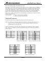
Map register located at I/O port 607h. The table below outlines the bits of the map register.
Memory Map Configuration Register, I/O Port 607 hex
BITS 1 & 0
Onboard Flash
DIP Socket
00
80000h - FFFFFh
OFF
01
F0000h - FFFFFh
E0000h - EFFFFh
10
OFF
80000h - FFFFFh
11
OFF
OFF
Table 1: Memory Map Configuration Register
In I/O space, the CPLD ports are located between 600h and 607h, the Ethernet controller is at
300h-30Fh. R8822 configuration and control registers are located from FF00h to FFFFh.
The PicoFlash uses Timer0 for the DOS timer tick and Timer2 as the timer tick prescaler. Timer1
is available for user applications.
I/O Configuration
The R8822 internal peripherals (UARTs, counter/timers, and interrupt controller) are not PC
compatible nor are they located at their traditional I/O port addresses.
For addressing and programming the peripherals specific to the R8822, please refer to the RDC
R8822 Microcontroller User’s Manual. The manual is available in PDF format on the
Development Kit CD or from our web site at http://www.jkmicro.com/documentation.
Digital I/O Ports
The picoFlash has a total of 16 bits of I/O generated by a CPLD. The board is also equipped with
an LED that can be used as a status indicator.
Hardware
5
JK microsystems
picoFlash User’s Manual
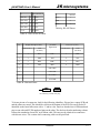
Ports A - D, 16 bits of I/O, are controlled by a CPLD. The I/O from the CPLD is grouped into
4-bit ports. Each of the four ports may be configured as either inputs or outputs. The following
tables show the port registers, addresses, and configuration bits.
Register
600h
601h
602h
603h
604h
605h
606h
Address
Port A
Port B
Port C
RESERVED
Port D
Clock/Calendar
I/O Config Register
I/O Configuration Register, READ/WRITE (I/O Port 606 hex)
Function
BIT
7
6
5
4
3
2
1
0
Bit is Clear
0
(default)
Disable
Port 605h
Clock
Access
Enable I/O
Connect
Connect
Port C on
J6-6 to
J6-8 to
J3
Port D bit 2 Port D bit 3
Port D
Input
Port C
Input
Port B
Input
Port A
Input
Bit is Set
1
Enable
Port 605h
Clock
Access
Connect
Connect
J6-6 to
RESERVED
J6-8 to
CPU
CPU INT2
TMROUT1
Port D
Output
Port C
Output
Port B
Output
Port A
Output
Table 2: I/O Configuration Register
Ports A through D each have a single data register that is read/write. Data read from the port
represents the current state of the port, data written to the port will be present on the port pins, if
the port is configured as an output. Each port may be configured as either an input or an output.
Write a 0 to the appropriate bit in the direction register to configure the port as an input, write a 1
to configure it as an output. All ports default to inputs.
!
The CPLD is a low power device that operates from 3.3 Volts. Although the inputs are 5V
tolerant, care must be taken to avoid exceeding the current specifications for the device.
Shorting an input to 5V will damage the CPLD.
LED, the LED at location DS1 is controlled by bit 10 of the PDATA1 register at 0FF7Ah. Set the
bit to turn the LED off, Clear the bit to turn the LED on.
Driving Loads with the I/O Ports
The ports on the picoFlash are capable of driving small loads or interfacing to TTL logic devices.
These ports can only source/sink a few milliamps. In order to interface with many loads,
additional circuitry, such as a transistor or relay, will be required. Designing the interface
between an output pin and a higher current load can present a challenge, especially if high speed
is required or the load is inductive in nature.
6
Hardware
JK microsystems
picoFlash User’s Manual
Switching inductive loads such as relays, solenoids and motors can generate transient voltages
many times larger than the steady-state operating voltage of the load. For example, turning off a
12 volt solenoid can easily create a negative spike of 200 volts. Worst case, these transients can
destroy your controller. In milder cases, they can cause program failures and flash memory
corruption. In the case of high current, high inductance devices, the spike need not even be
directly connected to the controller to cause damage or program failure.
!
Controllers damaged by inductive spikes are considered to be abused and are not eligible
for warranty repair.
A detailed study of dealing with inductive spikes is beyond the scope of this manual. For more
information, a good starting point is The Art Of Electronics, 2nd Ed. (Horwitz and Hill, 1989)
pages 52-53.
The following items should be considered when driving inductive loads:
A) When driving a DC inductive load, place a diode in parallel with the load. In most cases,
the diode can be a general purpose power diode such as a 1N4002. The cathode (banded
end) of the diode should connect to the positive side of the load. Locate the diode as
physically close to the load as possible. This applies to a small relay driven by a port pin,
as well as a larger inductive load connected to the contacts of a relay.
B) If you are using a relay to switch an AC-powered inductive load, put a varistor in parallel
with the load. The varistor voltage rating should be about 2 times the RMS (1.5 times the
peak-to-peak) steady-state voltage of the load.
C) Relays switching an inductive load may require a capacitor placed across their contacts.
0.1µF to 1.0µF is a good starting point. If the relays are switching an AC load, place a
100 ohm resistor in series with the capacitor.
D) Do not use the controller’s ground or power conductors to carry current from switched
inductive loads. Isolate these signals and route then directly to and from the power supply
and as far away from the controller as possible. A separate power source for large
inductive loads is strongly recommended. In the case of very large inductive loads, a
separate enclosure for the controller may be required.
Programming the I/O Ports
The I/O ports are located in the processor I/O space. Using the ports requires the use of functions
unique to the x86 family of processors. Creating a pointer to the location may seem logical, but
that reference would be in memory space, not I/O space. The Borland C functions inport(port)
and outport(port,value) are 16 bit (word) instructions, inportb(port) and
outportb(port,value) are 8 bit (byte) instructions. These functions are part of the dos.h
header file. Similar functions (and header files) are available for other C compilers and
languages. The following code illustrates the use of inportb() and outportb().
Hardware
7
JK microsystems
picoFlash User’s Manual
unsigned char port;
port = inportb(PORT_DIR);
port |= PORT_DIR_MASK;
outportb(PORT_DIR, port);
printf("PORT: 0x%X\n", (int)inportb(PORT));
!
/*
/*
/*
/*
get value of dir. reg */
set dir. bit for input */
write value to dir. reg */
read & print port value */
When changing any bit value in the R8822 PIO registers, it is essential that all of the
other bit values be preserved. You must read the 16-bit register, modify the desired bit(s),
and write the new value to the register.
Asynchronous Serial Ports
The picoFlash has 2 serial ports, Serial 0 and Serial 1. Both ports are internal to the R8822.
These UARTs are not compatible with the 16450 UARTs on a PC. The maximum data rate is
115k Baud at RS-232 levels.
Serial 0 is wired as Data Terminal Equipment (DTE) for connection to a peripheral such as a
modem. This port is jumper configurable to be either RS-232, TTL level RS-232 (RxD, TxD) or
half-duplex RS-485. When configured to use RS-232 levels, this is port implements the RTS,
CTS handshaking, and DCD control lines.
Serial 1 is wired as Data Communications Equipment (DCE) for direct connection to a computer
or terminal. This port is configured as a 3 wire RS-232 port implementing RxD and TxD.
The Serial Debug port does not make use of a hardware UART. It is intended for console and
debugging purposes only and should not be used in a design requiring high data throughput. Its
design generates an interrupt for each bit of serial data, and puts a large load on the processor
when data is being received. The port speed is fixed at 9600 baud.
Driver functions are available for Serial 0 and Serial 1 in the CSPD.COM TSR and related
CSPD***.LIB and .h files located in the picoFlash/drivers subdirectory on the utilities CD.
Please refer to the RDC R8822 data sheet for specific information on the serial ports and their
configuration.
RS-485 Configuration
The Serial 0 port of the picoFlash can be configured and used for RS-485 communications. To
configure Serial 0 as RS-485, move the jumper on JP1 to the 5-6 location. RS-485 signals are
present on J7. The RTS line on Serial 0 is used to control the RS-485 transmitter.
Library functions are available for use with RS-485 in the supplied driver.
The RS-485 driver is internally looped back. Characters transmitted will appear in the UART
receiver. This condition is inerrant to the RS-485 implementation and may present user
application implications.
8
Hardware
JK microsystems
picoFlash User’s Manual
Console Serial Port
As shipped, the default console port is Serial 1 at 9600 baud. To allow maximum flexibility, the
console can be located on either of the 2 hardware serial ports at a number of baudrates, or the
Debug port. When developing applications that require both hardware serial ports, it may be
helpful to move the console functions to the Debug Serial port. The Debug port (as described
previously) is implemented in software and has a fixed speed of 9600 baud.
To relocate the Console or change it’s baudrate, use the console.com utility and specify the
desired port, and if applicable, the baudrate. After a power cycle (or reset), the BIOS will use the
new console settings. See the examples below.
B:\>console 1 19200
Changes will take effect when board is rebooted
or
B:\>console D
Changes will take effect when board is rebooted
To see a usage message, do not specify any arguments.
B:\>console
PicoFlash Console Configuration V1.0
Usage: console port
Valid port ------>
Valid baudrates ->
For Ports
0 and 1
baudrate
0 1 D
300 600 1200 1800 2400 4800
7200 9600 19200 28800 38400
57600 76800 115200 153600
Baudrate for debug port is fixed at 9600
B:\>
Debug port signals are on J3 and require a special cable (PN: 86-0040) for connection to a PC.
!
The debug serial port is intended only for use as a development tool. While it is receiving
data, there is a high interrupt load. Other drivers that use interrupts (CSPD serial,
Ethernet, etc.) may cause disruptions with (or be disrupted by) the debug port.
Watchdog Timer
The R8822 is equipped with a watchdog timer that can be configured to generate either an NMI
or a processor reset. When enabled, software must keep the watchdog from timing out, indicating
proper operation. If the watchdog timer expires, the configured action will be taken. The
watchdog signal is not available external to the R8822, so a full board reset is not possible.
The watchdog control register is a word located at FFE6h. To Initialize the watchdog, first reset
the counter register by writing two words to the configuration register. Write an AAAAh
followed by a 5555h to the control register. Next, unlock the register by writing a 3333h followed
by a CCCCh to the control register. Finally, write the enable command to the watchdog
configuration register. The enable command is one word, with the high byte of C0h (enable
watchdog to generate system reset) and a low byte from the table below that represents the
Hardware
9
JK microsystems
Timeout
picoFlash User’s Manual
0x01
0x02
0x04
0x08
0x10
0x20
0x40
0x80
25uS
26mS
52mS
104mS
209mS
419mS 838mS 1.67S
Table 3: Watchdog timeout configuration
timeout interval. Software will then periodically reset the timer by writing two words to the
configuration register: AAAAh followed by 5555h. More details are available in the RDC R8822
Users Manual.
/* Watchdog Configuration Example */
#define WDTCON 0xFFE6
outport(WDTCON,
outport(WDTCON,
outport(WDTCON,
outport(WDTCON,
outport(WDTCON,
0xAAAA);
0x5555);
0x3333);
0xCCCC);
0xC080);
/* reset the watchdog timer */
/* unlock the control register */
/* set timeout of 1.67 seconds */
Ethernet
The Ethernet port is a 8-bit design that supports direct connection to a 10BASE-T network,
jumperless configuration, and NE2000 software compatibility. The controller has a base address
of 300h and processor interrupt 0, using full duplex twisted pair wiring supporting link detect.
The Ethernet controller requires a software driver to interface with network software or other
programs. The supplied packet driver (PICOPKT.COM) configures the chip interrupt, base address
and other necessary parameters.
To install the packet driver, type:
B:\> PICOPKT
The driver will install using INT 0, I/O base address 300h and will locate the MAC (Media
Access Control) number stored in the on board configuration EEPROM. Aceess to the driver will
be through software interrupt 60h. When the driver has loaded, it will indicate the MAC number,
port address, hardware and software interrupts.
B:\>PICOPKT
PicoFlash Ethernet Packet Driver v1.0
MAC=00:90:C2:40:13:C3 IO=300 HwInt=0 SwInt=0x60
After the driver has been installed, network software will be able to communicate with the
Ethernet adapter and the network. Users will probably want to modify their STARTUP.BAT file to
automatically load the packet driver.
The board has two LEDs that indicated the status of the Ethernet link. The LNK LED indicates
the status of the Ethernet. When illuminated, the picoFlash is receiving the Ethernet ‘heartbeat’
and is connected to a live network. If this LED is not illuminated, there is a problem with the
Ethernet wiring or the network. The ACT LED indicates activity on the network. The LED will
flash when a data packet is received or transmitted.
10
Hardware
JK microsystems
picoFlash User’s Manual
DiskOnChip
M-Systems’ DiskOnChip is a high performance single-chip Flash Disk. The DiskOnChip has
become the standard Flash Disk module for Embedded Single Board Computers. The
DiskOnChip is a Flash Disk in a standard 32-pin DIP package that has built-in TrueFFS (True
Flash File System) technology, allowing full read/write disk emulation.
The picoFlash currently supports the 8Meg Millennium DiskOnChip (MD2800-D08) with
version 4.2 (or earlier) firmware. Other DiskOnChip capacities will function if they are loaded
with the correct firmware, however M-Systems will not guarantee that the older firmware will
continue to be supported on parts other than the MD2800.
Install the DiskOnChip module in the memory expansion socket U6. Note the location of pin 1.
Set the Memory Type jumpers (JP2) for Flash memory. If the DiskOnChip is installed and
functioning, there will be an installation message that is displayed during the boot process and a
C: drive will be available to DOS.
picoFlash Bios Version 1.0
DOC Socket Services - Version 0.2
(C) Copyright 1992-1996, M-Systems Ltd.
TrueFFS-BIOS -- Version 3.3.9 for DiskOnChip 2000 (V4.2)
Copyright (C) M-Systems, 1992-2000
DOS Version 3.3e for JK microsystems Products
(C) HBS Corp and JK microsystems 1991-2002
B:\>
If, after the installation of a DiskOnChip, DOS fails to return a prompt, the DiskOnChip probably
has incompatible firmware and must be reformatted and it’s firmware reloaded.
Remove the DiskOnChip, reboot the board, and upload the file DOC.EXE from the utilities CD.
Power down the board, reinstall the DiskOnChip, and apply power while holding CNTL-C down.
Find the file DOC.EXE and execute it. It will extract 3 files. Execute the batch file FMT_DOC.BAT
and answer the prompts. This will format your DiskOnChip and load compatible firmware. You
may delete the 3 files after the operation is complete.
Jumpers
JP1 - Serial Port 0 Select, RS-485 Termination
This jumper selects the drivers and header that will be used for the Serial 0 signals and enables or
disables the RS-485 termination and biasing resistors. RS-485 termination is controlled by the
jumpers on pins 1-2 and 3-4. Install the jumpers to terminate the RS-485 signals and bias them to
the space state. Serial 0 can be jumpered as half-duplex RS-485, TTL RS-232 (Rx and Tx), or
RS-232 (Rx, Tx, RTS, CTS, DCD). Install the jumper at location 5-6 for RS-485 signals on J7,
7-8 for TTL RS-232 signals on J3 or 9-10 for RS-232 signals on J4.
Default position:
1-2 & 3-4, RS-485 termination enabled.
9-10, RS-232 Levels on J4.
NOTE: Only 1 jumper may be installed on JP1 pins 5-10.
Hardware
11
JK microsystems
picoFlash User’s Manual
JP2 - Socket Memory Type / Boot Memory Location
This jumper selects the type of memory in the expansion socket. Available choices are SRAM or
Flash. Other memory types may be supported if their pinout is compatible with standard SRAM
or Flash chips. Jumper pins 1-2 and 3-4 for SRAM or pins 1-3 and 2-4 for Flash. This jumper
also allows the board to boot from the expansion socket. This is useful when performing field
updates of the on-board Flash memory or when using an operating system other than DOS.
Jumper pins 5-7 and 6-8 to boot from the on-board memory or jumper pins 7-9 and 8-10 to boot
from the expansion socket.
Default position:
1-3 and 2-4, Flash memory expansion.
5-7 and 6-8, Boot from on-board flash.
Cables and Connectors
The following tables show the signal name (direction) for each connector pin.
NOTE: N/C indicates no connection and PULLUP indicates a 1k ohm pullup resistor to Vcc.
Outputs are driven by the board and received by a peripheral. Inputs are driven by a
peripheral and received by the board.
Serial 0 is configured as a DTE port, and is generally used to communicate with a peripheral
device. Serial 1 is configured as a DCE port, generally being used to connect the picoFlash to
another computer.
J1
Power
J2
Port A & B
J3
Debug & Port C
Vcc
1
PB.0
1
2 PA.0
Vcc
1
2 PC.0
RESET/
2
PB.1
3
4 PA.1
PC.1
3
4 PC.2
GND
3
PB.2
5
6 PA.2
PC.3
5
6 TTL TX
PB.3
7
8 PA.3
DBG RX
7
8 TTL RX
+5V
9
10 GND
DBG TX
9
10 GND
Table 4a: Power Pinout
Table 4b: Port A&B Pinout
J4
J5
Serial 0
Serial 1
DCD (in)
1
2 DSR (in)
PULLUP
1
2 N/C
RxD (in)
3
4 RTS (out)
TxD (out)
3
4 PULLUP
TxD (out)
5
6 CTS (in)
RxD (in)
5
6 PULLUP
DTR (out)
7
8 N/C
N/C
7
8 PULLUP
GND
9
10 N/C
GND
9
10 N/C
Table 4d: Serial 0 Pinout
12
Table 4c: Debug & PortC Pinout
Table 4e: Serial 1 Pinout
Hardware
JK microsystems
picoFlash User’s Manual
J6
JTAG & Port D
J7
RS-485
JTAG IN
1
2 PD.0
DATA +
1
JTAG OUT
3
4 PD.1
GND
2
JTAG CLK
5
6 PD.2
DATA -
3
JTAG RST
7
8 PD.3
+3.3V
9
10 GND
Table 4g: RS-485 Pinout
Table 4f: JTAG & Port D Pinout
J8
Straight Through (to Hub)
RJ-45 Pin #
Color
(86-0018)
1
1
BLU
2
2
3
4
picoFlash
Signal Name
Cross-Over (to PC)
RJ-45 Pin #
Color
(86-0018)
TxD +
3
BLK
ORG
TxD -
6
YEL
3
BLK
RxD +
1
BLU
6
YEL
RxD -
2
ORG
5
LNK LED +
6
LNK LED -
7
ACT LED +
8
ACT LED -
Table 4h: Ethernet Pinout
12345678
Pin numbering on RJ45 cable plug
To locate pin one of a connector, look for the following identifiers. Pin one has a square PCB pad
and the others are round. This should be visible on the bottom of the PCB. Pin one will also be
identified on the board silkscreen with a ‘1’ and/or a dot. Dual row headers have ODD numbered
pins on one side and EVEN numbered pins on the other. The dual row header numbering scheme
follows the numbering for an IDC style ribbon cable. This may not be identical on connectors
with discrete wires. Use caution when connecting cables to the picoFlash.
Hardware
13
JK microsystems
picoFlash User’s Manual
Software
Supported PC BIOS Functions
The picoFlash BIOS supports the following functions (software interrupts) common to PC
compatible computers. Please refer to a DOS/PC reference for more information on DOS and
BIOS software interrupts.
Int 10h, Video Driver, functions 9 and 0Eh
Int 11h, Get Equipment Configuration
Int 12h, Get Memory Size
Int 13h, Disk Driver, Functions 0-4
Int 14h, Serial Port Driver, Functions 0-3
Int 16h, Keyboard Driver, Functions 0 and 1
Int 19h, Boot System
Int 1Ch, Hook Timer Tick Interrupt
Driver Library
Drivers for the hardware serial ports and alphanumeric LCDs are supplied on the utilities CD in
the picoFlash\Drivers subdirectory.
For implementation details, see the README.TXT files and the driver source code for the
respective drivers.
Programming Languages
The picoFlash can be programmed in the language of your choice, as long as the compiler will
generate 16-bit DOS executables (.exe or .com).
A tutorial for getting started with the Borland 4.52 IDE is available on the development CD (see
\QuickStart.html) or from our website (http://www.jkmicro.com/documentation).
The WatTCP networking libraries are written in C and compiled with Borland 4.52. If you wish
to use a different version of Borland C, the libraries will need to be regenerated using that
compiler/linker/library manager.
14
Software
JK microsystems
picoFlash User’s Manual
QuickBASIC/PowerBASIC Console I/O
Some of the code produced by Microsoft QuickBASIC compiler does not execute properly on the
picoFlash. In the case of console I/O, we believe that QuickBASIC is generating code for specific
hardware and software not present on the picoFlash.
There are two problems with console I/O. The first is that a PRINT statement will not send output
to the console port. To output text to the console, open “cons:” as a file and print to it. The
second problem is that an INPUT statement will not echo the data entered by the user.
Workarounds for both of these problems can be found in the program BAS_INP.BAS on the
utilities CD /Example subdirectory and shown here:
start:
OPEN "o", 1, "cons:"
PRINT #1, ""
PRINT #1, "Quickbasic/PowerBasic Input Program"
PRINT #1, " Enter a string.........> ";
GOSUB linein
InputString$ = linein$
PRINT #1, InputString$
PRINT #1, " Enter a numeric value..> ";
GOSUB linein
InputNumber = VAL(linein$)
PRINT #1, InputNumber
CLOSE 1
END
linein:
linein$ = ""
linemore:
a$ = INKEY$
IF a$ = "" THEN GOTO linemore
IF a$ = CHR$(13) THEN GOTO linedone
IF a$ <> CHR$(8) THEN GOTO getchar
PRINT #1, CHR$(8); CHR$(32); CHR$(8);
linein$=left$(linein$,(len(linein$)-1))
GOTO linemore
getchar:
PRINT #1, a$;
linein$ = linein$ + a$
GOTO linemore
linedone:
PRINT #1, ""
RETURN
Software
15
JK microsystems
picoFlash User’s Manual
Utilities
The picoFlash comes preloaded with several utilities to aid system development. These utilities
are located on drive A: of the picoFlash and/or the development CD.
UP.COM
This utility facilitates uploading files to the picoFlash via the console port using the X-MODEM
transfer protocol. The utility requires the user to supply the name of the incoming file. Unless
otherwise specified, the file is placed in the active directory of the current drive. A write-protect
error will occur if UP tries to write to the read-only A: drive.
B:\>up
Upload file with X-MODEM Protocol
Usage: up file...
Version 3.0 for JK microsystems 186 products
B:\>up test.exe
Ready, start X-modem upload now,
Press CNTL-C to abort...
CCCC
B:\>
DOWN.COM
This utility facilitates downloading files from the picoFlash via the console port using the
X-MODEM transfer protocol. The utility requires the user to supply the name of the file to
transmit.
B:\>down
Download file with X-MODEM Protocol
Usage: down file...
Version 3.0 for JK microsystems 186 products
B:\>down test.exe
Ready, start X-modem download now,
B:\>
16
Utilities
JK microsystems
picoFlash User’s Manual
FORMAT.COM
If it becomes necessary to reformat the B: drive, FORMAT provides this function. CAUTION, all
information on the drive will be lost during the formatting process.
B:\>format
picoFlash FLASH Drive Format Program -Version 3.0
System will reboot after successful format...
Press 1 to initialize Drive B as 418 KB disk
Press ESC to exit with no changes
>1
Flash Drive is now formatted
Rebooting system...
EDIT.COM
A simple line editor is included to allow quick creation and modification of batch files or other
text files. EDIT is similar to Microsoft’s EDLIN provided in earlier versions of MS-DOS. It
allows list, insert, delete, and modify. Upon exit, a backup of the original file is created
(filename.BAK) and the edits are saved. If a backup file with the same name already exists, it is
overwritten. A list of commands and their usage is available by entering ‘h’ at the edit prompt
( >> ). The name of the file to edit must be supplied following the command EDIT on the
command line.
B:\>edit test.bat
FlashLite Line Editor v1.0
Enter h for help
New File: test.bat
>> iz
0: @echo Batch file being processed...
1: mytsr
2: myapp
3: ^Z
>> l
0: @echo Batch file being processed...
1: mytsr
-> 2: myapp
>> q
Save before exit (Y,n): y
File Saved
B:\>
Utilities
17
JK microsystems
picoFlash User’s Manual
DOS
JK microsystems’ controllers use XDOS, a compact operating system for embedded applications.
The XDOS command structure is nearly identical to MS/PC DOS version 3.3. The switches for
the DIR command have been changed and expanded. XDOS does not support redirected input or
output with the use of < and >, but does support pipes ( | ). None of the external DOS commands
are available due to size constraints. XDOS does not support installable file system functions.
XDOS Command Reference
In the list below, XDOS commands are followed by a function description and their format
including available parameters and switches. Items in boldface type must be entered. Capitals or
lowercase letters may be used. Items in italics are parameters. Those in boldface italics must be
entered, those in [ ] are optional. All switches are optional. They are shown as [/X]. Spaces and
punctuation are to be included. An ellipsis ... following items means that you may repeat the
items as often as needed. Do not enter the ellipsis or the square brackets. Most XDOS commands
allow the use of wildcards in filenames and extensions. When wildcards (?=one character, *=any
character or characters) are used, the command is executed once for each matching file.
Common parameters are:
[ d:]
drive specification - a letter followed by a colon (:), e.g. A:, if no drive is
specified, the default drive is used.
[path]
the path DOS must take in traveling from one directory to another; directory
names are separated by a backslash (\).
[filename] up to 8 characters used to name a file.
[.ext]
a three character extension may be added to a filename; an extension is
separated from a filename by a period.
CD / CHDIR
Function: Changes the current directory
Format: CD or CHDIR [[d:]path]
COPY
Function: Copies a file, combines two or more files into one file
Format: COPY
[d:][path]filename[.ext][switches]
[+[d:][path]filename[.ext][switches]
[d:][path][filename[.ext]][switches]
Switches: /V - verify the contents of new file
/A - copy file in ASCII format
/B - copy file in binary format
DATE
Function: Displays or changes the current DOS date.
Format: DATE [mm-dd-yyyy]
DEL / ERASE
Function: Deletes (erases) one or more files from a disk
Format: DEL or ERASE [d:][path][filename[.ext]]
18
DOS
JK microsystems
picoFlash User’s Manual
DIR
Function: Lists directory entries
Format: DIR [d:][path][filename[.ext]][switches]
Switches: /a - display file attributes
/b - sort by file size (in bytes)
/d - sort entries by date and time
/f - display entries by alphabetic file name order
/n - display entries in directory order (do not sort)
/s - include system and hidden files in output
/p - stop at end of each page
/w - display only the file name
/h - display Help screen (any invalid key)
MD / MKDIR
Function: Creates a subdirectory
Format: MD or MKDIR [d:]path
PATH
Function: Specifies directories DOS will search when trying to locate executable files
Format: PATH [[d:]path[;[d:]path ...]]
PROMPT
Function: Sets the DOS system prompt
Format: PROMPT [text]
Text:
Resulting Character(s):
$t The current time stored by DOS
$d The current date stored by DOS
$p The current directory
$v The version of DOS being used
$n The default drive
$g The character >
$l The character <
$b The character |
$q The character =
$$ The character $
$_ Carriage return plus line feed
DOS
19
JK microsystems
picoFlash User’s Manual
REN
Function: Renames a file
Format: REN [d:][path]filename[.ext] filename[.ext]
RD / RMDIR
Function: Deletes a subdirectory
Format: RD or RMDIR [d:]path
TIME
Function: Displays or changes the current DOS time
Format: TIME [hh:mm:ss.xx]
TYPE
Function: Display the contents of a file
Format: TYPE [d:][path]filename[.ext]
VER
Function: Displays the DOS version number
Format: VER
VOL
Function: Displays the volume label of specified drive
Format: VOL [d:]
20
DOS
JK microsystems
picoFlash User’s Manual
Specifications
Power Supply:
Operating Temperature:
Humidity:
5 VDC +/- 5% regulated, 2W (nominal)
-20 to +85 °C
5 - 90 % non-condensing
Port A,B,C,D:
Symbol
VIL
VIH
VOL
VOH
Parameter
Input Low
Input High
Output Low
Output High
MIN
0
2.0
MAX
0.8
5.5
0.4
2.4
Units
V
V
V
V
Condition
IOL= 8mA
IOH= -4mA
Mating Connectors:
Connector
2x5 Housing (J2- J6)
Mfg
MFG P/N
Molex 22-55-2101
Mfg
MFG P/N
Oupiin 4072-2X05H
JK micro P/N
28-0030
Pins
Molex 16-02-0096
Oupiin 404-PIN-10K
28-0033
1x3 Hou sing, Friction Lock (J1,7) Molex 22-01-2031
Oupiin 4071-03H
28-0012
1x8 Housing, Friction Lock (J8)
Molex 22-01-2081
Oupiin 4071-08H
28-0037
Pins, Friction Lock Housings
Molex 08-50-0114
Oupiin 4071-PIN-T
28-0013
Mechanical:
Dimensions
Weight
3.75” x 2.50" x 0.65”
95mm x 63.5mm x 16.5mm
1.8oz (51gm)
Specifications
21
JK microsystems
picoFlash User’s Manual
Contact Information
JK microsystems, Inc.
1403 Fifth Street, Suite D
Davis, CA 95616
Telephone:
Fax:
Email:
Web:
(530) 297-6073
(530) 297-6074
[email protected] (sales inquiries)
[email protected] (technical support)
http://www.jkmicro.com
M-Systems
DiskOnChip
39899 Balentine Drive, Suite 335
Newark, CA 94560
Telephone:
Fax:
Email:
Web:
Rev
----1.0
1.1
22
(510) 413-5950
(510) 413-5980
[email protected]
http://www.m-sys.com
Date
--------30NOV03
30JAN04
Author
-------EW
EW
Changes
----------------------------------------------------------First Issue
Add note on flash writes
Revise I/O tables, Add memory map config table
Contact Information