1
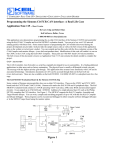
Errata Sheet
V 1.1, 2006-03
Device
C505A-4E
C505CA-4E
Marking/Step
Step CA
Package
P-MQFP-44
This Errata Sheet describes the deviations from the current user documentation.
The module oriented classification and numbering system uses an ascending sequence
over several derivatives, including already solved deviations. So gaps inside this
enumeration can occur.
Current Documentation
•
•
•
•
C505(C) User's Manual 08.97
C505A/C505CA Addendum to C505(C) User’s Manual 09.97
C505(A)/C505C(A) Data Sheet 12.02
Instruction Set Manual 07.00
Note: Devices marked with EES- or ES are engineering samples which may not be
completely tested in all functional and electrical characteristics, therefore they
should be used for evaluation only.
The specific test conditions for EES and ES are documented in a separate Status Sheet.
Contents
Section . . . . . . . . . . . . . . . . . . . . . . . . . . . . . . . . . . . . . . . . . . . . . . . . . . . . . . . . . . Page
History List/Change Summary . . . . . . . . . . . . . . . . . . . . . . . . . . . . . . . . . . . . . . . . . .2
Functional Deviations . . . . . . . . . . . . . . . . . . . . . . . . . . . . . . . . . . . . . . . . . . . . . . . . .4
Deviations from Electrical- and Timing Specification. . . . . . . . . . . . . . . . . . . . . . . .8
Application Hints . . . . . . . . . . . . . . . . . . . . . . . . . . . . . . . . . . . . . . . . . . . . . . . . . . . . .9
C505(C)A-4E, Step CA
1/9
V 1.1, 2006-03
Errata Sheet
History List/Change Summary
1
History List/Change Summary
(since last Step BB, previous Errata Sheet V1.0)
Table 1
Functional Deviations
Functional
Deviation
Short Description
CAN.2
Unexpected Remote Frame Transmission (C505CA
only)
CAN.3
Description in User's Manual regarding the reception
of remote frames and the data length code (DLC) field
is incorrect (C505CA only)
CAN.4
Flowchart sequence in figure in User's Manual
regarding Micro-controller handling of the Last
Message Object is partly incorrect (C505CA only)
CAN.5
Description in User's Manual section 6.4.5 regarding
the Configuration of the Bit Timing is partly incorrect
(C505CA only)
WDT.1
Watchdog Timer is not halted in Idle Mode
SWPD.1
Triggering of Software Power Down (SWPD) wake up
immediately after SWPD entry via external interrupt on
a frequent basis is not recommended.
OTP.1
OTP verification mode and verification error signaling
at Port 3.5
Table 2
AC/DC Deviations
AC/DC
Deviation
Short Description
DC.1
3 LSB total unadjusted error (TUE) of A/D converter
DC.2
VIH min on pin EA#
DC.3
VDD is valid for a smaller range than specified on
documents
C505(C)A-4E, Step CA
Fixed
Change
in Step
Fixed
Change
in Step
2/9
V 1.1, 2006-03
Errata Sheet
History List/Change Summary
Table 3
Application Hints
Application
Hint
Short Description
Hint 1
CAN clock on Pin 1.4 with bit TEST in SFR CR set
Hint 2
Content of VR2 register is incremented
C505(C)A-4E, Step CA
Fixed
Change
in Step
3/9
NEW
V 1.1, 2006-03
Errata Sheet
Functional Deviations
2
Functional Deviations
CAN.2: Unexpected Remote Frame Transmission (C505CA only)
The on-chip CAN module may send an unexpected remote frame with the identifier=0,
when a pending transmit request of a message object is disabled by software.
There are three possibilities to disable a pending transmit request of a message object
(n=1..14):
• Set CPUUPDn element
• Reset TXRQn element
• Reset MSGVALn element
Either of these actions will prevent further transmissions of message object n.
The symptom described above occurs when the CPU accesses CPUUPD, TXRQ or
MSGVAL, while the pending transmit request of the corresponding message object is
transferred to the CAN state machine (just before start of frame transmission). At this
particular time the transmit request is transferred to the CAN state machine before the
CPU prevents transmission. In this case the transmit request is still accepted from the
CAN state machine. However the transfer of the identifier, the data length code and the
data of the corresponding message object is prevented. Then the pre-charge values of
the internal “hidden buffer” are transmitted instead, this causes to a remote frame
transmission with identifier=0 (11 bit) and data length code=0.
This behavior occurs only when the transmit request of message object n is pending and
the transmit requests of other message objects are not active (single transmit request).
If this remote frame loses arbitration (to a data frame with identifier=0) or if it is disturbed
by an error frame, it is not retransmitted.
Effects to other CAN nodes in the network
The effect leads to delays of other pending messages in the CAN network due to the high
priority of the Remote Frame. Furthermore the unexpected remote frame can trigger
other data frames depending on the CAN node's configuration.
Workaround:
1. The behavior can be avoided if a message object is not updated by software when a
transmission of the corresponding message object is pending (TXRQ element is set)
and the CAN module is active (INIT = 0). If a re-transmission of a message (e.g. after
lost arbitration or after the occurrence of an error frame) needs to be cancelled, the
C505(C)A-4E, Step CA
4/9
V 1.1, 2006-03
Errata Sheet
Functional Deviations
TXRQ element should be cleared by software as soon as NEWDAT is reset from the
CAN module.
2. The nodes in the CAN system ignore the remote frame with the identifier=0 and no
data frame is triggered by this remote frame.
CAN.3: Description in User's Manual regarding the reception of remote frames and
the data length code (DLC) field is incorrect (C505CA only)
It is inaccurately described in the User's Manual on page 6-94 under 'Arbitration
Registers' that 'When the CAN controller stores a remote frame, only the data length
code is stored into the corresponding message object'. The correct should be that the
DLC field remains unchanged in the receiving message object, and that the CPU has the
responsibility to define the DLC of the answering data frame.
This correction will be updated to the future versions of the User's Manuals.
Workaround:
Not applicable.
CAN.4: Flowchart sequence in figure in User's Manual regarding Micro-controller
handling of the Last Message Object is partly incorrect (C505CA only)
For the software flowchart figure 6-37 in User's Manual 08.97, the correct would be to
first 'process message contents' and then to 'clear bit NEWDAT'.
process message
NEWDAT: = 0
This correction will be updated to the future versions of the User's Manuals.
Workaround:
Not applicable.
C505(C)A-4E, Step CA
5/9
V 1.1, 2006-03
Errata Sheet
Functional Deviations
CAN.5: Description in User's Manual section 6.4.5 regarding the Configuration of
the Bit Timing is partly incorrect (C505CA only)
As described for the CAN Bit Timing Register High BTR1, the minimum total time
requirement for segment 1 and segment 2 is as follows:
tTSeg1 ≥ 3 x tq
tTSeg2 ≥ 2 x tq
The total bit time remains at (tTSeg1 + tTSeg2 ≥ 7 x tq).
This correction will be updated to the future versions of the User's Manuals.
Workaround:
Not applicable.
WDT.1: Watchdog Timer is not halted in Idle Mode
The Watchdog Timer (WDT) is not halted in the Idle Mode as defined. However, during
the Idle Mode, an overflow condition of the WDT does not initiate an internal reset. In
such a case, the WDT starts a new count sequence.
Workaround:
1. Do not use the Watchdog Timer function in combination with the Idle Mode
2. In case of WDT is running before entry into idle mode, to avoid a WDT initiated reset
upon exit of the Idle Mode, the following methods can be used.
a) The WDT is refreshed immediately upon exit from Idle Mode.
b) A timed interrupt can be used to exit the Idle Mode before the WDT reaches the
counter state 7FFCh. This can be achieved by using Timer 0, 1 or 2. This timer can
be programmed to generate an interrupt at a WDT counter state prior to overflow,
for e.g., at 7F00h. Prior to entering Idle Mode, the WDT can be refreshed and Timer
0, 1or 2 can be started immediately to synchronize the WDT. In the interrupt service
routine of Timer 0, 1 or 2, the WDT must be refreshed. If required, Idle Mode could
be entered again.
C505(C)A-4E, Step CA
6/9
V 1.1, 2006-03
Errata Sheet
Functional Deviations
SWPD.1: Triggering of Software Power Down (SWPD) wake up immediately after
SWPD entry via external interrupt on a frequent basis is not recommended.
When the micro-controller is running at frequencies lower than 10MHz and the external
wake up from SWPD occurs very soon (e.g. <200ms) after entering this mode and this
happens on a regular basis, the internal clock may still be valid when the wake up trigger
occurs. In this rare case, the micro-controller may get confused with its state and
program execution becomes unpredictable.
Workaround:
In applications running at 10MHz or below, that enters and exits the SWPD mode on a
frequent basis, it is recommended to enter Slow Down mode before Power Down mode
entry. On SWPD wake up, the first instruction in the interrupt routine at 07bH should
disable Slow Down mode. This method would only cause an insignificant delay in the
range of ?s and would ensure specified behavior of the micro-controller. Note that when
Slow Down mode has been entered, there is no longer a minimum time requirement
before SWPD external wake up is triggered.
OTP.1: OTP verification mode and verification error signaling at Port 3.5
The last block of 16 bytes will always return verification error in the OTP verification
mode.
Workaround:
None.
C505(C)A-4E, Step CA
7/9
V 1.1, 2006-03
Errata Sheet
Deviations from Electrical- and Timing Specification
3
Deviations from Electrical- and Timing Specification
DC.1: 3 LSB total unadjusted error (TUE) of A/D converter
The total unadjusted error of the A/D converter does not meet the specified value of the
DC characteristics. The value for TUE is limited as follows:
TUE = 3 LSB in the VAIN range: VSS + 0.5V < VAIN < VDD - 0.5V
Workaround:
None.
DC.2: VIH min on pin EA#
The VIH min voltage on pin EA# does not meet the specified values :
VIH min for EA pin is 0.6 • VDD
(instead of 0.2 • VDD + 0.9 V)
Workaround:
None.
DC.3: VDD is valid for a smaller range than specified on documents
VDD is valid in the range from 4.5V to 5.5V at all specified temperatures, instead of
4.25V to 5.5V as specified on the documents. This smaller range is effective on devices
with date code starting from 0116.
Workaround:
None.
C505(C)A-4E, Step CA
8/9
V 1.1, 2006-03
Errata Sheet
Application Hints
4
Application Hints
Hint 1: CAN clock on Pin 1.4 with bit TEST in SFR CR set
A write to XRAM location F75FH will cause the CAN shift clock to be transmitted on Port
1.4 if the TEST bit in CAN control register CR is set. This TEST bit is for test purposes
only and should remain cleared in applications.
Workaround:
None.
Hint 2: Content of VR2 register is incremented
The VR2 register has a reset value of 13H.
Workaround:
None.
C505(C)A-4E, Step CA
9/9
V 1.1, 2006-03