1
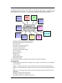
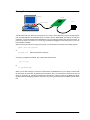
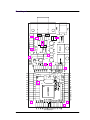
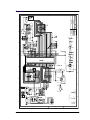
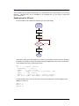
NMIN-2107
Single Board Computer
User Manual V.2
NMIN-2107
Nov 21, 2001
Table of Contents
Overview . . . . . . . . . . . . . . . . . . . . . . . . . . . . . . . . . . . . . . . . . . . . . . .
Included Files . . . . . . . . . . . . . . . . . . . . . . . . . . . . . . . . . . . . . . . . .
2
2
Getting Started . . . . . . . . . . . . . . . . . . . . . . . . . . . . . . . . . . . . . . . . . .
3
Memory Map . . . . . . . . . . . . . . . . . . . . . . . . . . . . . . . . . . . . . . . . . . . .
4
Programming the Board . . . . . . . . . . . . . . . . . . . . . . . . . . . . . . . . . .
ONCE Connector and Parallel Port . . . . . . . . . . . . . . . . . . . . . . . .
Modified S-Records and Serial Port . . . . . . . . . . . . . . . . . . . . . . . .
Transforming S-Records . . . . . . . . . . . . . . . . . . . . . . . . . . . . . . . . .
Hooking Into Autoboot . . . . . . . . . . . . . . . . . . . . . . . . . . . . . . . . . .
On-board Development System . . . . . . . . . . . . . . . . . . . . . . . . . . .
4
4
5
5
6
6
I/O Connections and Jumpers:. . . . . . . . . . . . . . . . . . . . . . . . . . . . .
Components . . . . . . . . . . . . . . . . . . . . . . . . . . . . . . . . . . . . . . . . . .
6
7
Board Layout . . . . . . . . . . . . . . . . . . . . . . . . . . . . . . . . . . . . . . . . . . .
8
Schematic . . . . . . . . . . . . . . . . . . . . . . . . . . . . . . . . . . . . . . . . . . . . . .
9
Examples . . . . . . . . . . . . . . . . . . . . . . . . . . . . . . . . . . . . . . . . . . . . . .
Reading from the A/D port . . . . . . . . . . . . . . . . . . . . . . . . . . . . . . .
10
10
User Manual V.2
Nov 21, 2001
1
Overview
The NMIN-2107 single computer board provides you with plug and play access to the powerful 32 bit
Motorola MMC2107 microcontroller. The computer board provides power regulation, RS232 and RS422
serial support and an LCD connector. The microcontroller includes the following built in capabilities:
port A
ONCE
A/D
port E
port B
MMC2107
Microcontroller
SPI
interrupts
port C
port D
•
•
•
•
•
•
•
•
•
•
•
•
•
timer
SCI
MCORE 32-bit RISC low-power integer processor
128K of block programmable (16K) flash memory
8K of static RAM
8 channels of 10-bit A/D with queueing
2 asynchronous serial channels
1 synchronous serial channel
8 timer channels with PWM capability
up to 40 interrupts
periodic interval timer
watchdog timer
35 digital I/O pins
eight external interrupts
ONCE debug support
The computer board’s power consumption with RS-422 drivers installed is about 80mA.
Included Files
The following files are included and are available from our website. The MaxForth file is only available if
you have licensed it.
• sloader.s - serial boot loader file in s-record format that can be downloaded through the ONCE port
• sloader.sp - serial bootloader file in modified s-record format that can be downloaded through the serial
port
• sikadown.pl - the Perl script used to modify s-records for downloading through the serial port and the
serial loader
• nmin2107.pdf - this manual in PDF format
• mfcoreapp.s - MaxForth in s-record format
• mfcoreapp.sp - MaxForth in modified s-record format
User Manual V.2
Nov 21, 2001
2
Getting Started
Computer
Board
MMC2107 (Sika) Flash Programmer
:
Power
Serial Cable
You will interact with your board by connecting it to a PC using a serial cable and running a terminal program
such as HyperTerminal or an equivalent setup. You need to set it to 19200 BAUD, one stop bit, no parity and
8 data bits. Connect an RS232 serial cable between your PC’s COM port and the serial port on the board. To
power up the board, you need a 9 to 12 volt plug in transformer plugged into the power jack, PJ1 (AC, DC
both polarities accepted).
When everything is ready and you plug in the power, you should receive a prompt in the terminal program.
MMC2107 (Sika) Flash Programmer
:
or
Max-FORTH V5.0N
(license agreement is required)
And when you depress the ENTER key, it should also response with
type ? for help
:
or
OK
(Max-FORTH prompt)
WHen you see that message, it means the communication is established and you are ready to interact with
the board and microcontroller. By pressing the reset button, SW1, you should get the same boot prompt as
when you powered it up. Pressing the reset button will leave the contents of most of the RAM intact which
might be useful for debugging purposes, whereas, if you power cycle the board, then all RAM contents will be
lost.
User Manual V.2
Nov 21, 2001
3
Memory Map
The memory map consists of the RAM, ROM and registers. The interrupt vectors can exist anywhere by
setting the vector base register (VBR).
0xFFFF.FFFF
External
Memory
0x8000.0000
Registers
0x00C0.0000
0x0080.1FFF
0x0080.0000
0x0001.FFFF
0x0000.4000
0
ports
Internal
RAM 8K
serial loader
Internal
Flash
128K
MaxForth or
Application
boot loader
Programming the Board
There are several ways in which to program the board:
1.
2.
3.
download an s-record through the ONCE connector and the PC parallel port with CPROGMCZ
download a modified s-record using the embedded bootloader and a serial port with
HyperTerminal
interact directly with the microcontroller and download source code to the on-board
development system, MaxForth, through a serial port and HyperTerminal
ONCE Connector and Parallel Port
Using the MCORE Cable from P&E Micro or equivalent, plug it into the parallel port of your computer
through a parallel port cable and the ONCE port on the computer board making sure to orientate the
triangle on the pin header to pin 1 on the board which is marked by a square solder pad on the bottom of
the board. Apply power to the board. When disconnecting from the board make sure it goes through a
power cycle before you try out the downloaded software as a reset is not enough to regain control of the
microcontroller after interacting with the ONCE port.
If you already have CPROGMCZ running, click reset the chip. If you start it up, it will reset the chip and
proceed to the next choice which is to read in a configuration file. The file that works with the board is the
MMC2107K_1.MCP file which should be in the directory for configuration files. Next you will need to
erase the module, specify an s-record to download and then program the module. To test out the
software, you must disconnect the ONCE connector and power cycle the board. The serial bootloader
User Manual V.2
Nov 21, 2001
4
file can be downloaded and then used to program the flash ROM using the serial port as described next.
Check the help screens for more details.
Modified S-Records and Serial Port
Using the serial bootloader, you can download s-records that have been created by a C compiler or
assembler system that you have acquired separately, to flash memory to be run. The help menu, invoked
by typing a ?, is:
: ?
To download to flash:
1. bulk erase if necessary
2. Make sure the delay time between lines
is set to at least 75 ms
3. Type f
4. Send S-record (processed with perl
script "sikadown.pl") as a text file
f - Program flash
v - Verify flash
b - bulk erase all of the flash
e - erase application from flash
:
When programming the flash with an s-record, the locations to be programmed should be erased to 0xFF
first by either erasing the whole flash or just all the sectors but the first one which contains the serial
bootloader.
WARNING
If you do bulk erase the entire flash with the ‘b’ selection, then the serial boot loader will be
gone and you will not be able to reboot. Your application should either put a vector at
location 0000, or you should download the serial bootloader program (sloader.sp).
The serial bootloader works by running out of RAM. At bootup, the startup program in flash checks to
see if there is an application at location 0x4000 by checking for a vector (anything but 0xFFFFFFFF). If
there isn’t, then it copies the serial bootloader program from flash to RAM and then runs the program.
The serial bootloader program must run out of RAM to be able to program flash memory.
If you erase all of flash, then the next time you reset the board, there will be no programs present and you
will have to program it through the ONCE port. Otherwise if you download a program with a reset vector
at location 0x00000000, such as the serial bootloader program, then it will boot up next time. You have
the flexibility to keep the serial bootloader program as part of your end system or to remove it and replace
it with another program. Any s-records that you do download to the board must be transformed by the
perl script, sikadown.pl.
Quick Tip !!
If you are using the serial boot loader to test out your application which starts with a vector at location
0x4000, then just use ‘e’ and ‘f’ to download your application.
If you download an application, reboot and nothing happens, you can recover to the serial boot loader by
shorting out PA7 to +3V on the J2 connector with a jumper or equivelant and pressing the reset button.
You will be taken back to the serial bootloader where you can erase your errant application and try again.
Transforming S-Records
To run the Perl script to transform your s-records into the required format for the serial downloader, you
will need to have Perl installed on your computer. You can get a copy of perl for your Windows, Linux or
Solaris platform from:
http://www.activestate.com/Products/ActivePerl/download.plex
User Manual V.2
Nov 21, 2001
5
To transform an s-record, you can type in the following commands in a DOS command window assuming
that Perl is installed and the script is running in the current directory:
\perl\bin\perl sikadown.pl sloader.s sloader.sp
The format of the command is Perl followed by the Perl script, then by the s-record file and finally by the
name of the transformed output file.
NOTE
If you include different memory regions in your code, make sure that your memory regions are
64 bytes or bigger as the perl script will mess up the translation from the S19 file to the
massaged s19 file. Compare the two if in doubt.
Hooking Into Autoboot
You can autoboot your application by leaving a vector to it at location 0x4000. The startup boot loader
will detect this vector and then jump to the location that the vector is pointing to. When MaxForth is
installed, it has a vector at that location. To get to the serial loader from MaxForth, type in FLASH and
enter. To get back to the serial loader from an application, execute the vector stored at location 0x190 in
memory. The application area, 0x0.4000-0x1.FFFF can be erased using the serial loader without the
boot loader being removed from memory.
On-board Development System
Taking advantage of the interactive nature of the board’s development system, MaxForth, you can
interact directly with the microcontroller’s peripherals by fetching and storing values to the configuration
registers for the peripheral devices. This is an effective way of understanding the peripheral
documentation, to verify correct initialization sequences, running some tests on different configurations
and debugging driver code as you develop it. By typing in new definitions, you can add new macros to
the dictionary for interactive use or for creating an automated program. Some examples are given later
on.
I/O Connections and Jumpers:
•
•
•
•
•
•
•
•
•
•
•
•
•
•
•
•
J1, LCD connector, match the triangle on the connector with the pin with a square solder pad.
J2, J3, J4 are general purpose I/O connectors including timers, A/D, INT, etc.
J5, RESET & GND pin not installed. It may be used as option for a front panel mounted reset switch.
J6, Misc. signals
J7, JTAG/Once
J8, includes jumper A, B, C. The Jumpers A,B,C allow both RS-232 drivers for COM1 & COM2 or 1 RS232 and 1 RS-422 driver for either COM.
Jumper A allows RS-422 selection of either TxD1 or TxD2 of SCI0 or SCI1 serial output signals
respectively.
Jumper B is the serial input to SCI1 labeled RxD2; it is defaulted to RS-232 but can be jumpered the
other way for RS-422. (Next to Jumper B is +5V & GND. This can be used for a test point or external
5V source to power a probe. Use a paper separator for protection.)
Jumper C is the serial input to SCI0 labeled RxD1. It is defaulted to RS-232 but can be jumpered for
other way for RS-422.
J9, Flash voltage supply. Connects when flash needs to Erase/Program. Open when flash does not
need to erase/program or for Write protection.
J10, serial connection for SCI1.
DB1, serial connection for SCI0.
J12, RS-232 shut down control input. Drive high for normal operation. Drive low to shut down the
drivers. This can be controlled by PA2 or jumper to 3V for normal operation (default).
J13, RS-422 connector
J14, Jumper to GND (default) for RS-422 receiver always or jumper to PA6 as RS-485 transmitter/
Receiver control signal.
J15 connects to pin 1 of RS-232, U2. This pin can be used to enable/disable the receivers for the RS-
User Manual V.2
Nov 21, 2001
6
232 interface. For normal operation, this pin must be low. By default, J15 is open and this pin is pulled
down through R5. To disable the receivers, J15 can be connected and controlled via PA0. Set it high to
disable and low to enable the receivers.
• J16 is only needed when U2, the RS-232 chip, is not installed and the LCD application required. Do
not connect J16 if U2 is present. This can damage U2.
Components
• SW1, reset switch
• RP1, 10K resistor pot for LCD contrast adjustment.
• U3, MAX4628 is the analog switch that provides the 5V to the flash VPP pin & A/D power source. This
allows the CPU to power up before the flash gets power and down after the power cuts off from the flash
to protect the flash from damage.
User Manual V.2
Nov 21, 2001
7
Board Layout
6
9
1
5
R7
R6
CR1
J15
J14
J13
U4
U5
C11
VR1
C10
C13
1
J10
C17
R5
C12
C14
U2
C15
A
C16
C9
B
RxD2
+5V GND
J9
1
C
R4
C7
U3
Q2
D1
J16
J7 1 V-
SW1
VR2
C8
J8
C6
L2
1
J6
GND
1
1
GND
+3V
PA6
PA7
PA4
PA5
PA2
PA3
PA0
PA1
PB6
PB7
C5
RN1
R3
1
L1
C3 C4 VRH
C1
R2
C2
PQA0
PQ
PQA3
PQ
PQB0
PQ
RN2PQB2
PQ
1
PE5
PE
PE7
SS
ST
J5
Q1
RP1
J1
U1
1
VR
PB4
PB5
PB2
PB3
SCK
PB0
PB1
MISO
MO
PC6
PC7
INT7
INT
PC4
PC5
INT5
INT
PC2
PA3
INT3
INT
PC0
PC1
INT1
INT
R1
1
J2
R0
J4
1
J3
User Manual V.2
Nov 21, 2001
8
User Manual V.2
Nov 21, 2001
A
B
C
D
J10
8
U2
DB1
3.3V
14
R7
13
10
5
6
19
15
12
3
7
20
PA2
PA0
C25,C28,C29
0.1UF
+5V
J12
A
3.3V
PA6
8
7
6
5
C
B
3.3V
R6
0.1UF
7
C24-C27,C31,C32
Q2
S80730AN
3.3V
J8
C14
C15
+3.3V
RxD2
TxD1
TxD2
RxD1
C16
3.3V
J14
1
2
3 MAX3483
4
U5
J13
7
C18,C20,C21,C22
AdditionalBypassCapacitors
GND
DTR
TX
RX
NC
8
9
16
17
4
C13
2
1
18
J15
6 7 8 9
1 2 3 4 5
R5
10K
0.1UF
+5V
NC
NC
CTS
RTS
DSR
U4
8
2
7
3MAX3483 6
4
5
1
C19,C23
3.3V
8
10K
R4
3.3V
RxD1
+5V
1
+5V
RxD2
6
MAX4628
U3
+5V
VDD
VDDF
VDD
TXD1
TXD2
ICOC10
ICOC12
ICOC20
ICOC22
PD0
PD2
PD4
PD6
GND
PA6
PA4
PA2
PA0
PB6
PB4
PB2
PB0
PC6
PC4
PC2
PC0
+5V
3.3V
R3
10K
3.3V
1
3.3V
PJ1
J9
VPP
CR1
5
R1
5
VM08/DB101
V-
RP1
10K
+5V
+5V
J16
.1uF
VSSA
C5
VDDA
9-12V
L1
10uH
10uH
L2
VSS
VSSF
RXD1
RXD2
TEST
ICOC11
ICOC13
ICOC21
ICOC23
PD1
PD3
PD5
PD7
PA7
PA5
PA3
PA1
PB7
PB5
PB3
PB1
PC7
PC5
PC3
PC1
VSS
J3
J2
LCDCONNECTOR
J1
PA7
NC
PB7
PB6
PB5
PB4
PB3
PB2
PB1
PB0
PA3
PA5
PA1
VO
NOTE:DonotconnectJ16ifU2isinstalled
6
100uF
C11
VPP
10K
PA6 1
PA5 2
PA4 3
PA3 4
PA2 5
PA1 6
PA0 7
PB7 8
PB6 9
PB5 10
PB4 11
VSS 12
VDD 13
PB3 14
PB2 15
PB1 16
PB0 17
PC7 18
PC6 19
PC5 20
VSS 21
VDD 22
PC4 23
PC3 24
PC2 25
PC1 26
PC0 27
PD7 28
PD6 29
PD5 30
PD4 31
PD3 32
PD2 33
PD1 34
PD0 35
ICOC23 36
ICOC22 37
ICOC21 38
ICOC20 38
ICOC13 40
ICOC12 41
ICOC11 42
ICOC10 43
TEST 44
TXD2 45
RXD2 46
TXD1 47
RXD1 48
INT0 49
INT1 50
IN
OUT
GND
4
PA7
DE
TRST
VDD
VSS
TMS
TDO
TDI
TCLK
VDD
CLKOUT
VSS
VSSSYN
EXTAL
XTAL
VDDSYN
RSTOUT
RESET
VDDA
VSSA
VRH
VRL
PQA0
PQA1
PQA3
PQA4
PQB0
PQB1
PQB2
PQB3
VDDH
PE5
PE6
PE7
SS
SCK
VSTBY
MISO
MISI
INT7
INT6
VPP
INT5
INT4
INT3
VDD
VSS
INT2
VDDF
VSSF
VR1
51
52
53
54
55
56
57
58
59
60
61
62
63
64
65
66
67
68
69
70
71
72
73
74
75
76
77
78
79
80
81
82
83
84
85
86
87
88
89
90
91
92
93
94
95
96
97
98
99
100
LM78L05
.1uF
C10
U1
4
D1
C9
.1uF
C8
3.3V
3.3V
1N5817
100uF
+5V
VDDA
1
3
IN
1
5
1
6
1 2
1
7
3
RP1
C6
3.3V
10Kx7
100uF
1
8
1 C1 2
22PF
10M
1 C2 2
22PF
R2
LM3940
OUT
GND
1
4
XTAL1
2 1
VSSSYN
RSTOUT
VSSA
VSSH
8Mhz
J6
VR2
1
RP2
2
VDDSYN
CLKOUT
1
VDDA
VDDH
3
.1uF
C7
3.3V
R0
10K
3.3V
2 3 4 5 6 7 8
1 1 1 1 1 1 1
3.3V
FINISH
2
C.N.
T.N.
APPROVALS
CHECKED
DRAWN
J7
2
GND
GND
GND
NC
TMS
DE
TRST
110601
110601
DATE
VDDA
VRH
PQA0
PQA3
PQB0
PQB2
PE5
PE7
SCLK
MISO
INT7
INT5
INT3
INT1
SCALE
D
SIZE
TITLE
J4
VSSA
VRL
PQA1
PQA4
PQB1
PQB3
PE6
SS
VSTB
MOSI
INT6
INT4
INT2
INT0
JTAG/OnCE
1
TDI
TDO
TCLK
GPIO/SI
RESET
VDD
GPIO/SO
SW1
NewMicros,Inc.
1601ChalkHillRd.
Dallas,TX.75212
www.newmicros.com
3.3V
10Kx7
2
3
DWGNO.
1
1SHEET
1OF1
01
REV
J5
optional
.001
C4
Q1
BBG06
NMIN-2107
MCORECPU
2
S80728AN
3.3V
1
A
B
C
D
Schematic
9
Examples
These examples may be typed in interactively or cut and pasted into the terminal window if you are using
MaxForth. Otherwise they can be translated to the language that you are using to program the
microcontroller with.
Reading from the A/D port
For this example we will consider the simplest way to get an A/D reading:
get A/D
reading
initialize
A/D
request
channel 0
channel
0?
not yet
display
reading
Done.
This involves: setting up the A/D registers so it is ready to go; requesting a read of a channel; waiting for
that channel to complete converting; and finally reading and displaying the value. Each of these boxes
on the diagram will become a word except for Done.
HEX
: H@
( a -- h )
: DISPLAY-READING
: CHANNEL0?
: CLEAR0
( -- )
( -- f )
( -- )
: REQUEST0
( -- )
: INIT-A/D
( -- )
: GETAD
COUNT 100 *
INIT-A/D
SWAP C@ OR ;
CA0280 H@ . ;
CA0010 C@ 80 AND ;
CHANNEL0?
CLEAR0
IF
2 CA0200 C!
REQUEST0
CA0010 DUP C@ 80 NOT AND SWAP C!
THEN ;
21 CA000C C! ;
C0 CA0201 C!
BEGIN
CHANNEL0?
2 CA0202 C!
UNTIL
FF CA0203 C! ;
DISPLAY-READING ;
The first reading is from 5 volts, the second from 0 volts and the third from 3.3 volts all applied to pin
PQB0 on connector J4.
GETAD 3D0
GETAD 21
GETAD 2A4
User Manual V.2
OK
OK
OK
Nov 21, 2001
10