1
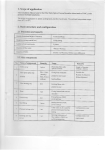
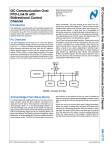
AN375 D E S I GN C ONSIDERATIONS FOR I SOLATING AN I2C BUS OR SMB US 1. Introduction I2C (inter-integrated circuit bus) was developed in the early 1980s1. In the early 1990s, Intel created an enhanced version of I2C called SMBus2 (system management bus) for power and thermal management systems in server and PC applications. In the early 2000s, SMBus2 was chosen as the physical interface for PMBus, an open specification for managing modular power systems, opening yet another market for I2C /SMBus products. Today, the venerable I2C bus continues to grow in popularity because of its low cost and overhead, strong industry support and relatively efficient communication protocol. As a result, I2C has been adopted in many new end applications. In many of these applications, I2C/SMBus interfaces require galvanic isolation for safety or ground loop elimination. For example, Power over Ethernet (PoE) applications typically use an I2C interface for communication between the PoE power sourcing device (PSE) and the earth-ground-referenced system controller. Galvanic isolation is required both by standard and also as a practical matter to prevent ground loops in Ethernet connected equipment. The physical interface consists of two wires: serial data (SDA) and serial clock (SCL). These wires are connected to open collector drivers that serve as both inputs and outputs. At first glance, it appears that SDA and SCL can be isolated simply by placing two unidirectional isolators in parallel and in opposite directions. However, this technique creates feedback that latches the bus line low when a logic low is asserted by either master or slave. This problem can be remedied by adding anti-latch circuits3 but results in a larger, more expensive solution. Recent breakthroughs in silicon RF isolation technology enable both the isolation and anti-latch functions to be integrated in single packages, such as the Silicon Laboratories Si8400 and Si8405 I2C bidirectional isolators4. These products offer a single-chip, anti-latch solution to the problem of isolating I2C /SMBus applications and require no external components except the I2C /SMBus pull-up resistors. In addition, the devices provide isolation to a maximum of 2.5 kVACRMS, support clock stretching, and operate to a maximum bus speed of 2 Mbps. This article describes the operation of integrated I2C isolators and the design constraints and considerations when using them. 2. I2C Isolator Operation Without anti-latch protection, bidirectional I2C isolators latch when an isolator output logic low propagates back through an adjacent isolator channel creating a stable latched low condition on both sides. Anti-latch protection is typically added to one side of the isolator to avoid this condition (the "A" side for the Si8400/05). To prevent the latch condition, the "A side" output low (VOL) and input low (VIL) levels are designed such that the isolator VOL is greater than the isolator VIL. Si8400/05 I2C/SMBus Unit 1 + - VIL ISO1 VOL VIL I2C/ SMBus Unit 2 VOL ISO2 Figure 1. I2C Example Implementation Using the Si8400/05 Rev. 0.2 10/09 Copyright © 2009 by Silicon Laboratories AN375 AN375 2.1. I2C Isolator Design Constraints Table 1 details the design constraints to consider when designing with I2C. Table 1. I2C Design Constraints and Effects Design Constraint To prevent the latch condition, the isolator output low level must be greater than the isolator input low level. Data Sheet Values Effect of Bus Pull-up Strength and Temperature Isolator VOL 0.8 V typical Isolator VIL 0.6 V typical This is normally guaranteed by the isolator data sheet. However, if the pull up strength is too weak, the outInput/Output Logic Low Level Differ- put low voltage will fall, and it can ence get too close to the input low logic ΔVSDA1, ΔVSCL1 = 50 mV minilevel. These track over temperature. mum The bus output low must be less Bus VOL = 0.4 V maximum than the isolator input low logic level. Isolator VIL = 0.45 V minimum If the pull up strength is too large, the devices on the bus might not pull the voltage below the input low range. These have opposite temperature coefficients. Worst case is high temperature. The isolator output low must be less Bus VIL 0.3 x VDD = 1.0 V minimum for VDD = 3.3 V than the bus input low. If the pull up strength is too large, the isolator might not pull the belowthe-bus input low voltage. Si8400/05 Vol: –1.8 mV/C CMOS buffer: –0.6 mV/C This gives some temperature tracking, but worst case is cold temperature. Isolator VOL = 0.825 V maximum, 0.5 mA pullup –10 °C to 125 °C 2.2. I2C Isolator Design Considerations The first step in applying an I2C isolator is to choose which side of the bus will be connected to the isolator A side. Ideally, it should be the side that: 1. Is compatible with the range of bus pull up specified by the manufacturer. For example, the Si8400/05 isolators are normally used with a pull up of 0.5 to 3 mA. 2. Has the largest input low level for devices on the bus. Some devices may specify an input low of 0.9 V, and other devices may require an input low of 0.3 x Vdd. Assuming a 3.3 V minimum power supply, the side with an input low of 0.3 x Vdd is the better side because this side has an input low level of 1.0 V. 3. Has devices on the bus that can pull down below the isolator input low level. For example, the Si840x input level is 0.45 V. Since most CMOS devices can pull to within 0.4 V of GND, this is generally not a problem. 4. Has the lowest noise. Due to the special levels, noise margins are reduced to as low as 50 mV. The Si840x isolators are not compatible with devices that have a logic low of 0.8 V. For this situation, a discrete circuit can be used.5 2 Rev. 0.2 AN375 2.3. Other System Level Design Considerations Two other important system level design considerations are clock stretching and accommodation of additional system status and control signals that typically require isolation. It is clear that the data line (SDA) needs to be bidirectional as this line contains data that can be either from the host to the slave or from the slave to the host. It is also common practice for the slave device to hold the clock line (SCL) low during the "acknowledge" (ACK) period while it is retrieving data for the master. For "clock stretching" to work in a particular I2C design, an I2C isolator that is also a bidirectional channel on the SCL line must be used. Without bidirectional isolation on the SCL signal, the designer must ensure that all I2C slaves can operate with the same bus clock rate and timing characteristics as the master. This places additional design and validation burdens on the system developer. The Si8400 is bidirectional for both SCL and SDA. Besides SCL and SDA signal isolation, many designs also require additional system status and control signals, such as resets and interrupt lines, to be isolated. The use of monolithic I2C isolators with additional unidirectional channels allows the system designer to simplify timing challenges in a design. Instead of being forced to isolate additional status and control channels in multiple isolator or opto-coupler packages (which results in significant part-to-part timing variations), monolithic I2C isolators with extra unidirectional channels exhibit timing characteristics that track very closely across process, voltage and temperature variations. The Si8405 has two additional unidirectional channels that are useful for isolating reset and interrupt signals. I2C design does not have to be a mystery. By considering each of these design tips and choosing an isolator appropriate to the demands, designers can easily implement I2C in their products. 3. References 1. NXP UM102104, I2C-bus specification and user manual, Rev. 03 - 19 June 2007 2. SMBus.org, "System Management Bus (SMBus) Specification", Version 2.0, August 3, 2000 3. John Gammel, "Adding bidirectional I2C digital isolation to your embedded design" Embedded.com Jan 30, 2009 4. Silicon Laboratories, Inc., Si8400/05 data sheet. 5. Silicon Laboratories, Inc., “AN352: Low-Cost, High-Speed I2C Isolation with Digital Isolators”. Rev. 0.2 3 AN375 DOCUMENT CHANGE LIST Revision 0.1 to Revision 0.2 4 Updated VIL and VOL levels to be consistent with latest data sheet. Rev. 0.2 AN375 NOTES: Rev. 0.2 5 AN375 CONTACT INFORMATION Silicon Laboratories Inc. 400 West Cesar Chavez Austin, TX 78701 Tel: 1+(512) 416-8500 Fax: 1+(512) 416-9669 Toll Free: 1+(877) 444-3032 Email: [email protected] Internet: www.silabs.com The information in this document is believed to be accurate in all respects at the time of publication but is subject to change without notice. Silicon Laboratories assumes no responsibility for errors and omissions, and disclaims responsibility for any consequences resulting from the use of information included herein. Additionally, Silicon Laboratories assumes no responsibility for the functioning of undescribed features or parameters. Silicon Laboratories reserves the right to make changes without further notice. Silicon Laboratories makes no warranty, representation or guarantee regarding the suitability of its products for any particular purpose, nor does Silicon Laboratories assume any liability arising out of the application or use of any product or circuit, and specifically disclaims any and all liability, including without limitation consequential or incidental damages. Silicon Laboratories products are not designed, intended, or authorized for use in applications intended to support or sustain life, or for any other application in which the failure of the Silicon Laboratories product could create a situation where personal injury or death may occur. Should Buyer purchase or use Silicon Laboratories products for any such unintended or unauthorized application, Buyer shall indemnify and hold Silicon Laboratories harmless against all claims and damages. Silicon Laboratories and Silicon Labs are trademarks of Silicon Laboratories Inc. Other products or brandnames mentioned herein are trademarks or registered trademarks of their respective holders. 6 Rev. 0.2