1
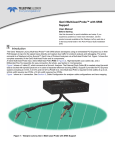
PCI Express 3.0 Mid-Bus Probe Installation and Usage Manual For use with Summit™ T3‐16 / T3‐8 / T34 Systems Generated: February 2, 2015, 13:36 Teledyne LeCroy Protocol Solutions Group Trademarks and Servicemarks Teledyne LeCroy, CATC Trace, PETracer, PETracer Summit, Summit T34, Summit T3‐8, Summit T3‐16, Universal Protocol Analyzer System, UPAS, and BusEngine are trademarks of Teledyne LeCroy. Microsoft and Windows are registered trademarks of Microsoft Corporation. Intel and Pentium are registered trademarks of Intel Corporation. All other trademarks and registered trademarks are property of their respective owners. THE SPECIFICATIONS AND INFORMATION REGARDING THE PRODUCTS IN THIS MANUAL ARE SUBJECT TO CHANGE WITHOUT NOTICE. ALL INFORMATION, EXAMPLES AND RECOMMENDATIONS IN THIS MANUAL ARE BELIEVED TO BE ACCURATE BUT ARE REPRESENTED WITHOUT WARRANTY OF ANY KIND, EXPRESS OR IMPLIED. USERS ARE FULLY RESPONSIBLE FOR THEIR APPLICATION OF ANY PRODUCTS. THE SOFTWARE LICENSE AND LIMITED WARRANTY FOR THE ACCOMPANYING PRODUCT ARE SET FORTH IN INFORMATION THAT SHIPPED WITH THE PRODUCT AND ARE INCORPORATED HEREIN BY THIS REFERENCE. IF YOU ARE UNABLE TO LOCATE THE SOFTWARE LICENSE OR LIMITED WARRANTY, CONTACT TELEDYNE LECROY FOR A COPY. © 2011 Teledyne LeCroy, Inc. All rights reserved. This document may be printed and reproduced without additional permission, but all copies should contain this copyright notice. WEEE Program Teledyne LeCroy 3385 Scott Blvd. Santa Clara, CA 95054 TEL: 800-909-7112 (USA and Canada) TEL: 408-653-1260 (worldwide) PCIe 3.0 Mid‐Bus Probe Installation and Usage Guide ii Contents Chapter 1: Introduction...........................................................................................1 1.1 Interposers .............................................................................................................................. 1 1.2 Specialty Probes..................................................................................................................... 1 1.3 PCIe Protocol Suite Analyzer Hardware and Software ....................................................... 1 1.4 Multi-Lead / Mid-Bus Probes ................................................................................................. 2 1.4.1 Complete Kits .........................................................................................................................................3 1.4.2 Individual Components ..........................................................................................................................4 Chapter 2: Probe Components ..............................................................................7 2.1 Probe Components................................................................................................................. 7 Chapter 3: Mechanical Design ...............................................................................9 3.1 Probe Footprints..................................................................................................................... 9 3.2 Mid-bus Probe Retention ..................................................................................................... 11 3.3 Probe Connection to Analyzer ............................................................................................ 13 3.4 Probe Keepout Volume ........................................................................................................ 13 3.5 Reference Clock Probe Attachment.................................................................................... 13 3.6 Daisy Chain Cable (for x16 applications) ........................................................................... 14 Chapter 4: Electrical Design.................................................................................17 4.1 Probe Loading Effect............................................................................................................ 17 4.2 Overview of Probe - Pin Assignments................................................................................ 17 4.3 Pin Assignments for Full-size Probe Connectors ............................................................. 18 4.4 Pin Assignments for Half-Size Probe Connectors ............................................................ 30 Chapter 5: Installation...........................................................................................35 PCIe 3.0 Mid‐Bus Probe Installation and Usage Guide iii Teledyne LeCroy Contents 5.1 Installation Steps for Mid-Bus Probe Pod and Related Components.............................. 35 5.2 Reference Clock Cable......................................................................................................... 38 5.3 Daisy-Chain Cable ................................................................................................................ 39 Chapter 6: Dual Probe Pod Setup Using External Clocking .............................41 Chapter 7: Recording Traffic................................................................................43 Chapter 8: Ordering Information .........................................................................45 Appendix A: How to Contact Teledyne LeCroy..................................................49 iv PCIe 3.0 Mid‐Bus Probe Installation and Usage Guide Chapter 1 Introduction Teledyne LeCroy offers a wide variety of ways to connect PCI Express protocol analyzers to products under test. There are four common methods: 1.1 Interposers Specialty Probes PCIe Protocol Suite Analyzer Hardware and Software Mid‐Bus Probes and Multi‐lead Probes Interposers If the product uses a standard PCI Express card connector, an interposer is used which is inserted between the PCIe Card and the card slot. The interposer taps off the data traffic to allow the analyzer to monitor and record traffic with minimal perturbation of the electrical interface. 1.2 Specialty Probes Specialty probes are used with specific card configurations, and are used in the same manner as an interposer card (in fact a specialty probe is an interposer card designed for a specific interface). Teledyne LeCroy supports a range of specialty probes including ExpressCard, AMC, XMC, Mini Card, External Cable, ExpressModule, HP Blade Server and SFF8639 interfaces. 1.3 PCIe Protocol Suite Analyzer Hardware and Software Designed for developers and validators, the Teledyne LeCroy Summit T3‐16™ is a Gen1/ Gen2/Gen3 PCI Express advanced verification system. By leveraging years of experience in protocol analysis tools for emerging markets, Summit T3‐16 blends sophisticated functionality with practical features to speed the development of PCI Express™ IP cores, semiconductors, bridges, switches, add‐in boards, and systems. PCIe 3.0 Mid‐Bus Probe Installation and Usage Guide 1 Teledyne LeCroy 1.4 Multi‐Lead / Mid‐Bus Probes Multi-Lead / Mid-Bus Probes The multi‐lead probe allows individual connections to each bus trace on the board. If the product has an embedded PCI Express bus (e.g., a bus which runs between chips on the same circuit board), then either a mid‐bus probe or a multi‐lead probe can be used. The mid‐bus probe requires a connection footprint (see below) to be designed into the board. The Teledyne LeCroy mid‐bus probes are 16‐channel differential signal probes that meet the demand for high‐density signal access, accuracy and repeatability while providing connector‐less attachment to the device under test. They are based upon the configuration that was initially recommended in the Intel PCI Express Mid‐Bus Probing Footprint and Pinout Revision 1.0 document dated 8/05/03 and the subsequent revisions. A mid‐bus probe is one of the tools that can greatly help engineers debugging PCI Express buses. A PCI Express mid‐bus probing solution provides direct probing capability of a PCI Express bus at a width of up to 16 lanes. To accommodate a mid‐bus probe, a special pad layout is required to expose the PCI Express differential pairs on the surface of the target board. (See figure below). Figure 1.1: Board Trace Layout for a Mid-Bus Probe Although not part of the PCI Express specifications, the industry has developed common mid‐bus probe footprints for PCIe 1.0a, PCIe 2.0 and PCIe 3.0 applications (the "full‐size" PCIe 3.0 footprint is shown on the right). These footprints are designed into the PCB. For PCIe 3.0 applications, the probe cable attachment uses a probe connector which is mounted the PCB as shown in the lower image on the below. Figure 1.2: Full Width Connector for a Mid-Bus Probe The appropriate footprint is recommended for use with all types of test equipment including protocol analyzers, logic analyzers and oscilloscopes. The required pad layout can be in x4 (half‐size), x8 (full‐size) or x16 (dual full‐size) configurations depending on the maximum number of lanes that need to be probed. All footprint sizes support probing at reduced lane widths (e.g., x1) and at lane widths up to the maximum footprint size. The illustration Figure 2.1 on page 7 shows the completed assembly for probing up to x8 configurations (for x16 configurations, a second Y‐cable, probe pod, header cable 2 PCIe 3.0 Mid‐Bus Probe Installation and Usage Guide Multi‐Lead / Mid‐Bus Probes Teledyne LeCroy assembly and probe connector are used, but connection is made to the same Summit T3‐16 analyzer ‐ see Figure 3.8 on page 15). As noted, a single full‐size probe connector supports up to x8 lane widths bidirectional, but can also be configured to support x16 unidirectional (as can a half‐size probe connector support x8 unidirectional). Note: This manual documents the mid‐bus footprint used for PCIe 3.0 applications; the probe footprints for PCIe 1.0a and PCIe 2.0 are covered in the Gen2 Mid‐Bus Probe User Manual. Teledyne LeCroy makes two versions of mid‐bus probes, one for PCIe 2.0 (2.5 and 5 GT/s data rates, also referred to as "Gen2") and one for PCIe 3.0 (2.5, 5 and 8 GT/s data rates, also referred to as "Gen3"). The PCIe 3.0 mid‐bus probe is for use with the Summit T3‐16, Summit T3‐8, Summit T34 analyzers, and is documented in this manual. The PCIe 3.0 mid‐bus probe, in a similar fashion to the PCIe 1.0a and PCIe 2.0 implementations that preceded it, is available in two versions: a full‐size probe and a half‐ size probe. The full‐size probe for is shown on Figure 2.1 on page 7. It has a four‐strand ribbon cable and a x16 connection header. A half‐size probe has a two strand ribbon cable and a x8 connection header. The part numbers and components of the Teledyne LeCroy PCIe 3.0 mid‐bus probes are as follows: 1.4.1 Complete Kits 1. PE090ACA‐X PCIe 3.0 Mid‐Bus Probe Kit* x8 Lane Width, Full‐size Connector, which includes: PE010UCA‐X: iPass Y‐Cable PE087ACA‐X: PCIe 3.0 Mid‐Bus Probe Pod with power supply PE057ACA‐X: PCIe 3.0 x8 Mid‐bus Probe Cable PE009UCA‐X: Daisy Chain Clock Cable PE014UCA‐X: Reference Clock Cable PE047UIA‐X: Gen3 Mid‐bus Probe Connector Full‐size * Supports up to x8 bi‐directional link or x16 uni‐directional link (for use with two Summit T34s, one T3‐8 or one T3‐16 analyzers). 2. PE094ACA‐X PCIe 3.0 Mid‐Bus Probe Kit* x4 Lane Width, Half‐size Connector, which includes: PE010UCA‐X: iPass Y‐Cable PE087ACA‐X: PCIe 3.0 x8 Mid‐Bus Pod with power supply PE056ACA‐X: Mid‐bus Probe Cable (x4) PE009UCA‐X: Daisy Chain Clock Cable PE014UCA‐X: Reference Clock Cable PE054UIA‐X: PCIe 3.0 Mid‐bus Probe Connector Half‐Size * Supports up to x4 bi‐directional link or x8 uni‐directional link (for use with one T3‐8 or one T3‐16 analyzer). PCIe 3.0 Mid‐Bus Probe Installation and Usage Guide 3 Teledyne LeCroy Multi‐Lead / Mid‐Bus Probes 3. PE091ACA‐X PCIe 3.0 Mid‐Bus Probe Kit* x4 Lane Width, Half‐size Connector, which Includes: PE013UCA‐X: x4‐to‐x8 Straight iPass Cable PE087ACA‐X: PCIe 3.0 x8 Mid‐Bus Pod with power supply PE056ACA‐X: Mid‐bus Probe Cable (x4) PE009UCA‐X: Daisy Chain Clock Cable (second cable for future expandability) PE014UCA‐X: Reference Clock Cable (second cable for future expandability) PE054UIA‐X: PCIe 3.0 Mid‐bus Probe Connector Half‐Size * Supports up to x4 bi‐directional link or x8 uni‐directional link (for use with one Summit T‐34 analyzer only). TABLE 1.1: Full Size Probe Kit Capabilities x1 Uni x Bidir x PE090ACA-X PCIe 3.0 x8 Full-Size Probe Kit x2 x4 x8 Uni Bidir Uni Bidir Uni Bidir x x x x x x x16 Uni x Bidir * *: For bidirectional x16, two PE090ACA‐X kits are required. TABLE 1.2: Half Size Probe Kit Capabilities PE094ACA-X / PE091ACA-X PCIe 3.0 x4 Half-Size Probe Kit x1 x2 x4 x8 x16 Uni Bidir Uni Bidir Uni Bidir Uni Bidir Uni Bidir x x x x x x x 1.4.2 Individual Components 1. PE087ACA‐X PCIe3 Mid‐bus Pod with Thumbscrews No cables (for use with Summit T3‐16 or Summit T3‐8), includes power supply. 2. PE056ACA‐X PCIe3 Mid‐bus Probe Cable with Thumbscrews G3x4 probe cable (Half size ‐‐ connects to G3 Mid‐bus box, for use with Summit T34, Summit T3‐16 or Summit T3‐8) 3. PE057ACA‐X PCIe3 Mid‐bus Probe Cable with Thumbscrews G3x8 probe cable (Full size ‐‐ connects to G3 Mid‐bus box, for use with Summit T3‐16 or Summit T3‐8) 4. PE038UIA‐X PCIe Gen3 x8 Dish for Mid‐bus Probe 5. PE047UIA‐X Gen3 Mid‐bus Probe Connector Full‐Size 4 PCIe 3.0 Mid‐Bus Probe Installation and Usage Guide Multi‐Lead / Mid‐Bus Probes Teledyne LeCroy 6. PE054UIA‐X Gen3 Mid‐bus Probe Connector Half‐Size 7. PE010UCA‐X Y‐Cable from Mid‐bus Probe Pod to Analyzer 8. PE013UCA‐X x4‐to‐x8 Straight iPass Cable PCIe 3.0 Mid‐Bus Probe Installation and Usage Guide 5 Teledyne LeCroy 6 Multi‐Lead / Mid‐Bus Probes PCIe 3.0 Mid‐Bus Probe Installation and Usage Guide Chapter 2 Probe Components 2.1 Probe Components Y‐Cable to Analyzer Gen3 Mid‐Bus Probe Pod Probe Header Cable Assembly Probe Connector (mounted to board) Clocking Cable Cable* (not shown) Summit T3‐16 (shown), Summit T3‐8, or Summit T34 Analyzers Mid‐bus Probe Pod (PE087ACA‐X) Y‐Cable to Summit T3‐16 or Summit T3‐8 Analyzers (PE010UCA‐X) Connect “A” Side to “UPSTREAM” and “B” side to “DOWNSTREAM” Probe Header Cable Assembly (PE057ACA‐X) PCIe Probe Connector (PE047UIA‐X) Figure 2.1: Typical Full Size Probe Components PCIe 3.0 Mid‐Bus Probe Installation and Usage Guide 7 Teledyne LeCroy Probe Components Note: * The Intel‐based mid‐bus footprint specification only supplies differential lane signaling and ground reference. Should a reference clock (RefClk) be required a separate connection must be made. Teledyne LeCroy PCI Express protocol analyzers can use a reference clock probe in conjunction with the mid‐bus analysis. Each mid‐bus probe is equipped with one clock probe. The mid‐bus reference clock probe is designed to facilitate capturing clock signals from the system board in the two configurations recommended by the Intel guideline, i.e., a tap off of an existing clock or a dedicated clock. 8 PCIe 3.0 Mid‐Bus Probe Installation and Usage Guide Chapter 3 Mechanical Design This section describes footprint dimensions, keepout volumes, and probe pin assignments. 3.1 Probe Footprints The Mid‐bus Probe is fully compatible with the standardized mid‐bus footprint recommended by the Intel guideline, as shown in the following figures. Full-Size Probe Footprint Figure 3.1: PCIe Gen 3 Footprint PCIe 3.0 Mid‐Bus Probe Installation and Usage Guide 9 Teledyne LeCroy Probe Footprints PCIe Gen 3 Full Size Keepout Volume Figure 3.2: PCIe Gen 3 Keepout Volume Half-Size Probe Footprint Figure 3.3: PCIe Gen 3 Half Width Footprint 10 PCIe 3.0 Mid‐Bus Probe Installation and Usage Guide Mid‐bus Probe Retention Teledyne LeCroy PCIe Gen 3 Half Size Keepout Volume Figure 3.4: PCIe Gen 3 Half Width Probe Keepout Volume PCB Layout of Full Size PCIe Gen 3 Mid-bus Footprint Figure 3.5: Full Size PCIe Gen 3 PCB Footprint PCB Layout of Half Size PCIe Gen 3 Mid-bus Footprint Figure 3.6: Half Size PCIe Gen 3 PCB Footprint 3.2 Mid-bus Probe Retention To prepare a circuit board for PCI Express mid‐bus probing, the mid‐bus footprint has to be laid out onto the target system board and a probe connector has to be attached to the board. Attachment of the probe connector is simple and quick. There are two through‐ hole screws and one protrusion key underneath the probe connector. Align the key of the probe connector with the keying/alignment hole in the mid‐bus footprint on the target system board, and connect the small screws (supplied) through the PCB and into the threaded holes on the underside of the Mid‐bus connector module, and tighten the screws to ensure good contact between the contacts of the connector and the pads on PCIe 3.0 Mid‐Bus Probe Installation and Usage Guide 11 Teledyne LeCroy Mid‐bus Probe Retention the PCB. The mid‐bus probe can then be attached to the target system board through the probe connector to provide mechanical support for pin‐to‐pin alignment. The mid‐bus cable has 2 retention screws that connect to the probe connector to hold the probe in place. Cable to PCB Connector Figure 3.7: Cable Connection to PCB Connector Note: The attachment screws supplied will provide secure attachment for most PCB designs. If the PCB is very thick, the screws may not be long enough to pass through the PCB and securely attach the Mid‐bus connector module, in which cases longer screws will be needed. The screws supplied are 5mm long (McMaster‐Carr P/N 91292A005), and longer lengths can be obtained directly from McMaster‐Carr in 6mm (91292A006), 8mm (91292A008), or longer lengths as needed. The probe connector should not be confused with a PCB connector because it is not part of the electrical circuits of either the target system or the probe. PCIe 3.0 probe connectors can be purchased through Teledyne LeCroy: 12 Full‐size: P/N PE047UIA‐X Half‐size: P/N PE054UIA‐X PCIe 3.0 Mid‐Bus Probe Installation and Usage Guide Probe Connection to Analyzer 3.3 Teledyne LeCroy Probe Connection to Analyzer The bus signals captured by the mid‐bus probe are connected to a mid‐bus probe pod for amplification. This reduces the load imposed by the mid‐bus probe on the target system, while allowing a longer cable to attach to the Teledyne LeCroy PCI Express protocol analyzer. The Teledyne LeCroy PCI Express protocol analyzer can then interpret these signals for full decoding and protocol analysis. 3.4 Probe Keepout Volume As with any connection to a PCB, sufficient clearance must be allowed around the point where the probe will connect. This is defined as the keep‐out volume, which must be kept clear of other components mounted on the PCB. The probe keepout volumes are shown in the diagrams in “Probe Footprints” on page 9. 3.5 Reference Clock Probe Attachment Should SSC clocking be used in the system under test or if the link varies the bit rate by more than 100 MHz ± 300ppm (see Section 4.3.7 of Base Spec 3.0), a reference clock tap may be required. The connection from the reference clock to the analyzer is a 3‐pin header (1 by 3, 0.050” center spacing) which is placed on the clock signal transmission line of the DUT. The PE014UCA‐X Reference Clock Cable provides a three‐pin micro socket that connects from this header to the CLK IN port on the Mid‐Bus Pod. If the reference clock is sampled by tapping off an existing clock, the header shall be located on the existing clock transmission line, where a high impedance clock probe from the mid‐bus probe is connected with no significant loading effects. In the case of a dedicated clock, the header shall be located at the end of a dedicated clock transmission line without termination, where a 50‐Ohm cable is connected and the termination for the clock signal is provided on the mid‐bus probe board. The connectivity of the clock header pins follows the following table: TABLE 3.3: Clock Header Pins Signal REFCLKp Unused REFCLKn Pin Number 1 (or 3) 2 3 (or 1) Note: The analyzer is not sensitive to the polarity of the reference clock. Therefore, the probe can be plugged onto the pin header in either orientation. The following 3‐pin header can be used for the reference clock: Samtec Part No: TMS‐103 (Vertical Orientation) PCIe 3.0 Mid‐Bus Probe Installation and Usage Guide 13 Teledyne LeCroy Daisy Chain Cable (for x16 applications) The reference clock is captured separately with a dedicated probe cable. Considering the possibility that one clock may be shared between two physically separated mid‐bus probes, each mid‐bus probe pod is equipped with a reference clock output port. The reference clock probe can capture signals from the target system or receive a duplicated reference clock from another mid‐bus probe board. 3.6 Daisy Chain Cable (for x16 applications) A single mid‐bus probe pod can capture traffic on bus widths up to x8. If x16 lane widths are required (e.g., when using a Summit T3‐16 Analyzer with a x16 device), two Mid‐Bus Probe Pods are required. In this configuration, one of the pods is connected to the DUT to tap the Reference Clock signal, and the second pod is "daisy‐chained" to the first pod using the PE009UCA‐X Daisy Chain Cable. Connect the Ref Clock cable to the CLK IN port of the first pod, and connect the Daisy Chain Cable between the CLK OUT port of the first pod and the CLK IN port of the second pod. 14 PCIe 3.0 Mid‐Bus Probe Installation and Usage Guide Daisy Chain Cable (for x16 applications) Teledyne LeCroy Mid-bus Probe Setup for x16 lane widths (using Summit T3-16 Analyzer, Clocking Cable not shown) Figure 3.8: Mid-bus Probe Setup for x16 lane widths PCIe 3.0 Mid‐Bus Probe Installation and Usage Guide 15 Teledyne LeCroy 16 Daisy Chain Cable (for x16 applications) PCIe 3.0 Mid‐Bus Probe Installation and Usage Guide Chapter 4 Electrical Design 4.1 Probe Loading Effect The logical probing of the PCI Express bus is achieved by tapping a small amount of energy from the probed signals and channeling this energy to the analyzer. To avoid excessive loading conditions, the Teledyne LeCroy mid‐bus probe employs high impedance tip resistors (isolation resistors). The probe isolation resistance is selected to both satisfy the probe sensitivity and system parasitic load requirements. Extensive care has been taken to reduce the parasitic effect of the probed signals during each phase of the mid‐bus probe design. The equivalent load model of the Mid‐bus probe is available in HSPICE parameters. It is an empirical‐based model that involves complicated connectivity. It can be requested from the Teledyne LeCroy Protocol Systems Group support team ([email protected]) With this unique design, the Teledyne LeCroy mid‐bus probes can capture bus traffic signals with amplitudes specified by the PCI Express standard, while introducing only slight loss and jitter on the channel under test. To determine the exact numbers, customers are encourage to simulate their channel using Teledyne LeCroy’s model. 4.2 Overview of Probe - Pin Assignments Cross‐references from the PCI Express Mid‐Bus Probing Footprint and Pinout (8/05/03) Revision 1.0 are given in tables listed below. The Summit T3‐16 PCI Express analyzers from Teledyne LeCroy support a lane swizzling feature which allows pairs of differential pin assignments to be re‐wired dynamically to match the configuration under the probe. This also provides additional versatility in the case where two busses are mapped to the probe footprint and cannot be uniquely positioned within a quadrant. Lane swizzling allow you to reorder upstream lanes or recorder downstream lanes regardless of the order of physical connections – however, you cannot interchange upstream lanes with downstream lanes. In the pinout tables that follow, the following variations may be applied: The designation of upstream and downstream may be reversed as long as it is reversed for every lane (all upstream connections on the left and all downstream on the right may be swapped). Lane ordering may be reversed if done as a whole such that probe lanes 0, 1, 2, 3, 4, 5, 6, 7 connect to physical lanes 7, 6, 5, 4, 3, 2, 1, 0. PCIe 3.0 Mid‐Bus Probe Installation and Usage Guide 17 Teledyne LeCroy Pin Assignments for Full‐size Probe Connectors Note: The Summit T3‐16 analyzer provides the flexibility to reorder lanes regardless of the order in which they are physically connected (lane swizzling). 4.3 Each differential signal pair may have the D+ and D‐ assignment reversed. Pin Assignments for Full-size Probe Connectors For x16 lane widths, two full‐size headers are required. The diagrams below show the recommended pin assignments for x16 configurations (keep in mind that any of modifications mentioned in Overview of Probe ‐ Pin Assignments can be applied, and in addition the lane swizzling feature of the Summit T3‐16 system noted in “Overview of Probe ‐ Pin Assignments” on page 17). TABLE 4.4: Table Legend For All Pinout Tables Character C Ln U D p n 18 Function Channel Lane Upstream Downstream Positive Polarity Negative polarity PCIe 3.0 Mid‐Bus Probe Installation and Usage Guide Pin Assignments for Full‐size Probe Connectors Teledyne LeCroy TABLE 4.5: General 16 Channel PCIe Pinout Pin # Signal Name A1 A2 A3 A4 A5 C1p C1n GND Cp2 Cn2 A6 A7 A8 A9 A10 C5p C5n GND C6p C6n A11 A12 A13 A14 A15 C9p C9n GND C10p C10n A16 A17 C13p C13n A18 A18 A20 GND C14p C14n PCIe 3.0 Mid‐Bus Probe Installation and Usage Guide B1 B2 B3 Signal Name GND C0p C0n B4 B5 B6 B7 B8 C3p C3n GND C4p C4n B9 B10 B11 B12 B13 C7p C7n GND C8p C8n B14 B15 B16 B17 B18 C11p C11n GND C12p C12n B19 B20 B21 C15p C15n GND Pin # 19 Teledyne LeCroy Pin Assignments for Full‐size Probe Connectors TABLE 4.6: x16 (One Uni-Directional) Specific 16 Channel PCIe Pinout Pin # 20 Signal Name A1 A2 A3 A4 A5 Ln1p Ln1n GND Ln2p Ln2n A6 A7 A8 A9 A10 Ln5p Ln5n GND Ln6p Ln6n A11 A12 A13 A14 A15 Ln9p Ln9n GND Ln10p Ln10n A16 A17 Ln13p Ln13n A18 A18 A20 GND Ln14p Ln14n B1 B2 B3 Signal Name GND Ln0p Ln0n B4 B5 B6 B7 B8 Ln3p Ln3n GND Ln4p Ln4n B9 B10 B11 B12 B13 Ln7p Ln7n GND Ln8p Ln8n B14 B15 B16 B17 B18 Ln11p Ln11n GND Ln12p Ln12n B19 B20 B21 Ln15p Ln15n GND Pin # PCIe 3.0 Mid‐Bus Probe Installation and Usage Guide Pin Assignments for Full‐size Probe Connectors Teledyne LeCroy TABLE 4.7: x8 (One Bi-Directional) Specific 16 Channel PCIe Pinout Pin # Signal Name A1 A2 A3 A4 A5 Ln0p‐D Ln0n‐D GND Ln1p‐D Ln1n‐D A6 A7 A8 A9 A10 Ln2p‐D Ln2n‐D GND Ln3p‐D Ln3n‐D A11 A12 A13 A14 A15 Ln4p‐D Ln4n‐D GND Ln5p‐D Ln5n‐D A16 A17 Ln6p‐D Ln6n‐D A18 A18 A20 GND Ln7p‐D Ln7n‐D PCIe 3.0 Mid‐Bus Probe Installation and Usage Guide B1 B2 B3 Signal Name GND Ln0p‐U Ln0n‐U B4 B5 B6 B7 B8 Ln1p‐U Ln1n‐U GND Ln2p‐U Ln2n‐U B9 B10 B11 B12 B13 Ln3p‐U Ln3n‐U GND Ln4p‐U Ln4n‐U B14 B15 B16 B17 B18 Ln5p‐U Ln5n‐U GND Ln6p‐U Ln6n‐U B19 B20 B21 Ln7p‐U Ln7n‐U GND Pin # 21 Teledyne LeCroy Pin Assignments for Full‐size Probe Connectors TABLE 4.8: x8 (Two Uni-Directional) Specific 16 Channel PCIe Pinout Pin # 22 Signal Name A1 A2 A3 A4 A5 Ln1p‐1 Ln1n‐1 GND Ln2p‐1 Ln2n‐1 A6 A7 A8 A9 A10 Ln5p‐1 Ln5n‐1 GND Ln6p‐1 Ln6n‐1 A11 A12 A13 A14 A15 Ln1p‐2 Ln1n‐2 GND Ln2p‐2 Ln2n‐2 A16 A17 Ln5p‐2 Ln5n‐2 A18 A18 A20 GND Ln6p‐2 Ln6n‐2 B1 B2 B3 Signal Name GND Ln0p‐1 Ln0n‐1 B4 B5 B6 B7 B8 Ln3p‐1 Ln3n‐1 GND Ln4p‐1 Ln4p‐1 B9 B10 B11 B12 B13 Ln7p‐1 Ln7n‐1 GND Ln0p‐2 Ln0n‐2 B14 B15 B16 B17 B18 Ln3p‐2 Ln3n‐2 GND Ln4p‐2 Ln4n‐2 B19 B20 B21 Ln7p‐2 Ln7n‐2 GND Pin # PCIe 3.0 Mid‐Bus Probe Installation and Usage Guide Pin Assignments for Full‐size Probe Connectors Teledyne LeCroy TABLE 4.9: x4 (Two Bi-Directional) Specific 16 Channel PCIe Pinout Pin # Signal Name A1 A2 A3 A4 A5 Ln0p‐D1 Ln0n‐D1 GND Ln1p‐D1 Ln1n‐D1 A6 A7 A8 A9 A10 Ln2p‐D1 Ln2n‐D1 GND Ln3p‐D1 Ln3n‐D1 A11 A12 A13 A14 A15 Ln0p‐D2 Ln0n‐D2 GND Ln1p‐D2 Ln1n‐D2 A16 A17 Ln2p‐D2 Ln2n‐D2 A18 A18 A20 GND Ln3p‐D2 Ln3n‐D2 PCIe 3.0 Mid‐Bus Probe Installation and Usage Guide B1 B2 B3 Signal Name GND Ln0p‐U1 Ln0n‐U1 B4 B5 B6 B7 B8 Ln1p‐U1 Ln1n‐U1 GND Ln2p‐U1 Ln2p‐U1 B9 B10 B11 B12 B13 Ln3p‐U1 Ln3n‐U1 GND Ln0p‐U2 Ln0n‐U2 B14 B15 B16 B17 B18 Ln1p‐U2 Ln1n‐U2 GND Ln2p‐U2 Ln2n‐U2 B19 B20 B21 Ln3p‐U2 Ln3n‐U2 GND Pin # 23 Teledyne LeCroy Pin Assignments for Full‐size Probe Connectors TABLE 4.10: x4 (Four Uni-Directional) Specific 16 Channel PCIe Pinout Pin # 24 Signal Name A1 A2 A3 A4 A5 Ln1p‐1 Ln1n‐1 GND Ln2p‐1 Ln2n‐1 A6 A7 A8 A9 A10 Ln1p‐2 Ln1n‐2 GND Ln2p‐2 Ln2n‐2 A11 A12 A13 A14 A15 Ln1p‐3 Ln1n‐3 GND Ln2p‐3 Ln2n‐3 A16 A17 Ln1p‐4 Ln1n‐4 A18 A18 A20 GND Ln2p‐4 Ln2n‐4 B1 B2 B3 Signal Name GND Ln0p‐1 Ln0n‐1 B4 B5 B6 B7 B8 Ln3p‐1 Ln3n‐1 GND Ln0p‐2 Ln0p‐2 B9 B10 B11 B12 B13 Ln3p‐2 Ln3n‐2 GND Ln0p‐3 Ln0n‐3 B14 B15 B16 B17 B18 Ln3p‐3 Ln3n‐3 GND Ln0p‐4 Ln0n‐4 B19 B20 B21 Ln3p‐4 Ln3n‐4 GND Pin # PCIe 3.0 Mid‐Bus Probe Installation and Usage Guide Pin Assignments for Full‐size Probe Connectors Teledyne LeCroy TABLE 4.11: x4 (Two Uni-Directional) Specific 16 Channel PCIe Pinout Pin # Signal Name A1 A2 A3 A4 A5 Ln1p‐1 Ln1n‐1 GND Ln2p‐1 Ln2n‐1 A6 A7 A8 A9 A10 NC NC GND NC NC A11 A12 A13 A14 A15 Ln1p‐2 Ln1n‐2 GND Ln2p‐2 Ln2n‐2 A16 A17 NC NC A18 A18 A20 GND NC NC PCIe 3.0 Mid‐Bus Probe Installation and Usage Guide B1 B2 B3 Signal Name GND Ln0p‐1 Ln0n‐1 B4 B5 B6 B7 B8 Ln3p‐1 Ln3n‐1 GND NC NC B9 B10 B11 B12 B13 NC NC GND Ln0p‐2 Ln0n‐2 B14 B15 B16 B17 B18 Ln3p‐2 Ln3n‐2 GND NC NC B19 B20 B21 NC NC GND Pin # 25 Teledyne LeCroy Pin Assignments for Full‐size Probe Connectors TABLE 4.12: x2 (Two Bi-Directional) Specific 16 Channel PCIe Pinout Pin # 26 Signal Name A1 A2 A3 A4 A5 Ln0p‐D1 Ln0n‐D1 GND Ln1p‐D1 Ln1n‐D1 A6 A7 A8 A9 A10 NC NC GND NC NC A11 A12 A13 A14 A15 Ln0p‐D2 Ln0n‐D2 GND Ln1p‐D2 Ln1n‐D2 A16 A17 NC NC A18 A18 A20 GND NC NC B1 B2 B3 Signal Name GND Ln0p‐U1 Ln0n‐U1 B4 B5 B6 B7 B8 Ln1p‐U1 Ln1n‐U1 GND NC NC B9 B10 B11 B12 B13 NC NC GND Ln0p‐U2 Ln0n‐U2 B14 B15 B16 B17 B18 Ln1p‐U2 Ln1n‐U2 GND NC NC B19 B20 B21 NC NC GND Pin # PCIe 3.0 Mid‐Bus Probe Installation and Usage Guide Pin Assignments for Full‐size Probe Connectors Teledyne LeCroy TABLE 4.13: x2 (Four Uni-Directional) Specific 16 Channel PCIe Pinout Pin # Signal Name A1 A2 A3 A4 A5 Ln1p‐1 Ln1n‐1 GND NC NC A6 A7 A8 A9 A10 Ln1p‐2 Ln1n‐2 GND NC NC A11 A12 A13 A14 A15 Ln1p‐3 Ln1n‐3 GND NC NC A16 A17 Ln1p‐4 Ln1n‐4 A18 A18 A20 GND NC NC PCIe 3.0 Mid‐Bus Probe Installation and Usage Guide B1 B2 B3 Signal Name GND Ln0p‐1 Ln0n‐1 B4 B5 B6 B7 B8 NC NC GND Ln0p‐2 Ln0n‐2 B9 B10 B11 B12 B13 NC NC GND Ln0p‐3 Ln0n‐3 B14 B15 B16 B17 B18 NC NC GND Ln0p‐4 Ln0n‐4 B19 B20 B21 NC NC GND Pin # 27 Teledyne LeCroy Pin Assignments for Full‐size Probe Connectors TABLE 4.14: x1 (Two Bi-Directional) Specific 16 Channel PCIe Pinout Pin # 28 Signal Name A1 A2 A3 A4 A5 Ln0p‐D1 Ln0n‐D1 GND NC NC A6 A7 A8 A9 A10 NC NC GND NC NC A11 A12 A13 A14 A15 Ln0p‐D2 Ln0n‐D2 GND NC NC A16 A17 NC NC A18 A18 A20 GND NC NC B1 B2 B3 Signal Name GND Ln0p‐U1 Ln0n‐U1 B4 B5 B6 B7 B8 NC NC GND NC NC B9 B10 B11 B12 B13 NC NC GND Ln0p‐U2 Ln0n‐U2 B14 B15 B16 B17 B18 NC NC GND NC NC B19 B20 B21 NC NC GND Pin # PCIe 3.0 Mid‐Bus Probe Installation and Usage Guide Pin Assignments for Full‐size Probe Connectors Teledyne LeCroy TABLE 4.15: x1 (Four Uni-Directional) Specific 16 Channel PCIe Pinout Pin # Signal Name A1 A2 A3 A4 A5 NC NC GND NC NC A6 A7 A8 A9 A10 NC NC GND NC NC A11 A12 A13 A14 A15 NC NC GND NC NC A16 A17 NC NC A18 A18 A20 GND NC NC PCIe 3.0 Mid‐Bus Probe Installation and Usage Guide B1 B2 B3 Signal Name GND Ln0p‐1 Ln0n‐1 B4 B5 B6 B7 B8 NC NC GND Ln0p‐2 Ln0n‐2 B9 B10 B11 B12 B13 NC NC GND Ln0p‐3 Ln0n‐3 B14 B15 B16 B17 B18 NC NC GND Ln0p‐4 Ln0n‐4 B19 B20 B21 NC NC GND Pin # 29 Teledyne LeCroy 4.4 Pin Assignments for Half‐Size Probe Connectors Pin Assignments for Half-Size Probe Connectors TABLE 4.16: Table Legend for all Half-Size Probe Connectors Character C Ln U D p n Function Channel Lane Upstream Downstream Positive Polarity Negative polarity TABLE 4.17: General 8 Channel PCIe Gen3 Pinout 30 Pin # Signal Name A1 A2 A3 A4 A5 C1p C1n GND C2p C2n A6 A7 A8 A9 A10 C5p C5n GND C6p C6n Pin # B1 B2 B3 Signal Name GND C0p C0n B4 B5 B6 C3p C3n GND B7 B8 C4p C4n B9 B10 B11 C7p C7n GND PCIe 3.0 Mid‐Bus Probe Installation and Usage Guide Pin Assignments for Half‐Size Probe Connectors Teledyne LeCroy TABLE 4.18: x8 (One Uni-Directional) Specific 8 Channel PCIe Pinout Pin # Signal Name A1 A2 A3 A4 A5 Ln1p‐1 Ln1n‐1 GND Ln2p‐1 Ln2n‐1 A6 A7 A8 A9 A10 Ln5p‐1 Ln5n‐1 GND Ln6p‐1 Ln6n‐1 B1 B2 B3 Signal Name GND Ln0p‐1 Ln0n‐1 B4 B5 B6 B7 B8 Ln3p‐1 Ln3n‐1 GND Ln4p‐1 Ln4n‐1 B9 B10 B11 Ln7p‐1 Ln7n‐1 GND Pin # TABLE 4.19: x4 (One Bi-Directional) 8 Channel PCIe Pinout Pin # Signal Name A1 A2 A3 Ln0p‐D1 Ln0n‐D1 GND A4 A5 Ln1p‐D1 Ln1n‐D1 A6 A7 A8 A9 A10 Ln2p‐D1 Ln2n‐D1 GND Ln3p‐D1 Ln3n‐D1 PCIe 3.0 Mid‐Bus Probe Installation and Usage Guide Pin # B1 B2 B3 Signal Name GND Ln0p‐U1 Ln0n‐U1 B4 B5 B6 B7 B8 Ln1p‐U1 Ln1n‐U1 GND Ln2p‐U1 Ln2n‐U1 B9 B10 B11 Ln3p‐U1 Ln3n‐U1 GND 31 Teledyne LeCroy Pin Assignments for Half‐Size Probe Connectors TABLE 4.20: x4 (Two Uni-Directional) Specific 8 Channel PCIe Pinout Pin # Signal Name A1 A2 A3 A4 A5 Ln1p‐1 Ln1n‐1 GND Ln2p‐1 Ln2n‐1 A6 A7 A8 A9 A10 Ln1p‐2 Ln1n‐2 GND Ln2p‐2 Ln2n‐2 B1 B2 B3 Signal Name GND Ln0p‐1 Ln0n‐1 B4 B5 B6 B7 B8 Ln3p‐1 Ln3n‐1 GND Ln0p‐2 Ln0n‐2 B9 B10 B11 Ln3p‐2 Ln3n‐2 GND Pin # TABLE 4.21: x2 (Two Bi-Directional) Specific 8 Channel PCIe Pinout 32 Pin # Signal Name A1 A2 A3 Ln0p‐D1 Ln0n‐D1 GND A4 A5 Ln1p‐D1 Ln1n‐D1 A6 A7 A8 A9 A10 Ln0p‐D2 Ln0n‐D2 GND Ln1p‐D2 Ln1n‐D2 Pin # B1 B2 B3 Signal Name GND Ln0p‐U1 Ln0n‐U1 B4 B5 B6 B7 B8 Ln1p‐U1 Ln1n‐U1 GND Ln0p‐U2 Ln0n‐U2 B9 B10 B11 Ln1p‐U2 Ln1n‐U2 GND PCIe 3.0 Mid‐Bus Probe Installation and Usage Guide Pin Assignments for Half‐Size Probe Connectors Teledyne LeCroy TABLE 4.22: x1 (Two Bi-Directional) Specific 8 Channel PCIe Pinout Pin # Signal Name A1 A2 A3 A4 A5 Ln0p‐D1 Ln0n‐D1 GND NC NC A6 A7 A8 A9 A10 Ln0p‐D2 Ln0n‐D2 GND NC NC B1 B2 B3 Signal Name GND Ln0p‐U1 Ln0n‐U1 B4 B5 B6 B7 B8 NC NC GND Ln0p‐U2 Ln0n‐U2 B9 B10 B11 NC NC GND Pin # TABLE 4.23: x1 (Four Bi-Directional) Specific 8 Channel PCIe Pinout Pin # Signal Name A1 A2 A3 Ln0p‐D1 Ln0n‐D1 GND A4 A5 Ln0p‐D2 Ln0n‐D2 A6 A7 A8 A9 A10 Ln0p‐D3 Ln0n‐D3 GND Ln0p‐D4 Ln0n‐D4 PCIe 3.0 Mid‐Bus Probe Installation and Usage Guide Pin # B1 B2 B3 Signal Name GND Ln0p‐U1 Ln0n‐U1 B4 B5 B6 B7 B8 Ln0p‐U2 Ln0n‐U2 GND Ln0p‐U3 Ln0n‐U3 B9 B10 B11 Ln0p‐U4 Ln0n‐U4 GND 33 Teledyne LeCroy 34 Pin Assignments for Half‐Size Probe Connectors PCIe 3.0 Mid‐Bus Probe Installation and Usage Guide Chapter 5 Installation To install the Mid‐Bus Probe follow the steps below: 5.1 Installation Steps for Mid-Bus Probe Pod and Related Components 1. Install probe connector into PCI Express target system board. Figure 5.1: Full Width Connector for a Mid-Bus Probe The probe connector allows the Teledyne LeCroy mid‐bus probe to attach to the target system board. The probe connector is installed by aligning the module pins with the holes on the target system board. The probe connector is keyed ‐ so be sure to orient it so that it matches the connector. 2. Bolt the probe connector to the board. 3. Plug the mid‐bus probe header into the probe connector as shown below. PCIe 3.0 Mid‐Bus Probe Installation and Usage Guide 35 Teledyne LeCroy Installation Steps for Mid‐Bus Probe Pod and Related Components Figure 5.2: Cable Connection to PCB Connector 4. Carefully tighten the probe to the target by using the two thumbscrews. The thumbscrews should be screwed in only finger‐tight. Caution:The probe is delicate equipment. Please tighten the thumbscrew carefully while watching the LEDs on the probe pod. Over‐tightening the probe header might damage the miniature probing spring pins. 36 PCIe 3.0 Mid‐Bus Probe Installation and Usage Guide Installation Steps for Mid‐Bus Probe Pod and Related Components Teledyne LeCroy 5. Connect the four probe cables to the mid‐bus probe pod ports marked A[0‐3], B[0‐3], A[4‐7] and B[4‐7], using the labels on the cables to match each cable to the correct connector on the pod. The mid‐bus probe pod amplifies the signal and sends it to the analyzer. The PCIe 3.0 (Gen3) probe pod is shown below. Figure 5.3: Mid-Bus Probe Pod and Associated Cables to DUT 6. If you intend to use the analyzer's reference clock, connect the three pin clock cable to the port marked "Clk In" (Reference Clock In) on the mid‐bus probe pod. 7. Connect the other end of the clock cable to the three‐pin reference clock header on the PCI Express board. Orientation of the cable does not matter. 8. Connect the single‐headed end of the Y‐cable to the pod port marked "Analyzer." See figure on next page. PCIe 3.0 Mid‐Bus Probe Installation and Usage Guide 37 Teledyne LeCroy Reference Clock Cable Figure 5.4: Mid-Bus Probe Pod with Cable to Analyzer 9. Connect the other ends of the cable to the analyzer as follows: The "A" side of the cable plugs into the Upstream 0‐7 and the "B" side of the cable plugs into the Downstream 0‐7 ports on the Summit Analyzer. If using two Gen3 Probe pods for x16 applications on a Summit T3‐16 Analyzer, connect the second probe pod using the Upstream 8‐16 and Downstream 8‐16 ports on the Summit T3‐16 Analyzer. When using a Summit T34 Analyzer just connect the straight cable between the pod and the analyzer. 5.2 Reference Clock Cable The Reference Clock Cable (PE014UCA‐X) connects the Mid‐Bus Pod to the DUT so that the pod can use the clock from the DUT. The cable has a 3‐pin micro socket at one end that attaches to a 3‐pin header (0.050" spacing) designed into the DUT, and the other end connects to the Clk In port on the Mid‐Bus Probe Pod, as shown below. Figure 5.5: Reference Clock Cable 38 PCIe 3.0 Mid‐Bus Probe Installation and Usage Guide Daisy‐Chain Cable 5.3 Teledyne LeCroy Daisy-Chain Cable The Daisy Chain Cable (PE009UCA‐X) connects multiple Mid‐Bus Pods together so they can share the same clock. One end of the connector is attached to the Clk Out port of the Mid‐Bus Pod supplying the clock signal, and the other end is connected to the Clk In port of the other Mid‐Bus Pod, as shown below. PCIe 3.0 Mid‐Bus Probe Installation and Usage Guide 39 Teledyne LeCroy 40 Daisy‐Chain Cable PCIe 3.0 Mid‐Bus Probe Installation and Usage Guide Chapter 6 Dual Probe Pod Setup Using External Clocking The steps outlined above in Chapter 5, “Installation,” on page 35 describe a single Probe/ single Analyzer configuration. In a dual analyzer setup, a second probe may need to be added depending on the type of link that is being recorded. If the analyzer internal clock is to be used, then cable the target device to the probe pod as follows ‐ however, omit the 3‐pin reference clock cable(s) shown in the illustration. If external clocking is to be used, using the PE014UCA‐X Ref Clock cable, connect the 3‐pin reference clock cable from the 3‐pin header on the system board to the CLK IN port on one probe pod. Then using the PE009UCA‐X Daisy Chain Cable, connect the CLK OUT port on that same pod and connect it to the CLK IN port on the second pod. The setup is shown below. PCIe 3.0 Mid‐Bus Probe Installation and Usage Guide 41 Teledyne LeCroy Figure 6.1: Dual Probe Pod Configuration 42 PCIe 3.0 Mid‐Bus Probe Installation and Usage Guide Chapter 7 Recording Traffic For instructions on setting up and implementing a recording, please refer to the user manual for the Teledyne LeCroy protocol analyzer being used. PCIe 3.0 Mid‐Bus Probe Installation and Usage Guide 43 Teledyne LeCroy 44 PCIe 3.0 Mid‐Bus Probe Installation and Usage Guide Chapter 8 Ordering Information Use the following table of part numbers and descriptions to order components for Teledyne LeCroy PCIe 3.0 Mid‐bus probes. Ordering Information Table 8.1, “Ordering Information ‐‐ Analyzers and Probes,” on page 46 and Table 8.2, “Ordering Information ‐ Cables and Accessories,” on page 47. PCIe 3.0 Mid‐Bus Probe Installation and Usage Guide 45 Teledyne LeCroy TABLE 8.1: Ordering Information -- Analyzers and Probes Gen3 Analyzers PE050AAA‐X PE051AAA‐X PE060AAA‐X PE061AAA‐X PE062AAA‐X PE080AAA‐X PE081AAA‐X Summit T3‐16 (licensed as a Gen3 x16 analyzer, no probes or cables) Summit T3‐16 (licensed as a Gen3 x8 analyzer, no probes or cables) Summit T3‐8 (licensed as a Gen3 x8 analyzer, no probes or cables) Summit T3‐8 (licensed as a Gen3 x4 analyzer, no probes or cables) Summit T3‐8 (licensed as a Gen3 x1 analyzer, no probes or cables) Summit T34 (licensed as a Gen3 x4 analyzer, no probes or cables) Summit T34 (licensed as a Gen3 x1 analyzer, no probes or cables) Gen3 Mid-Bus Probes PE087ACA‐X PCIe3 Mid‐bus Pod with Thumbscrews, no cables (for use with Summit T3‐16, Summit T3‐8 or Summit T34), includes power supply. PE090ACA‐X PCIe3 Full‐size Mid‐bus Probe Kit [includes Mid‐bus pod with Thumbscrews, iPass Y‐cable, power supply, G3x8 Probe Cable, Full‐size Probe Connector, Ref Clock Cable and Daisy Chain Clock Cable (for connecting two pods to support bi‐ directional x8)]. Supports up to bi‐directional x8 link or uni‐directional x16 link (for use with Summit T3‐8 or T3‐16). PE091ACA‐x PCIe3 Half Size Mid‐bus Probe Kit [includes Mid‐bus pod with Thumbscrews, iPass Straight Cable, power supply, G3x4 Probe Cable, Half‐size Probe Connector, two (2)Ref Clock Cables and two (2) Daisy Chain Clock Cables (to connect two pods to support bi‐directional x8)]. Supports up to Bi‐directional x4 link or Uni‐directional x8 link. For use with Summit T34 systems only. PE094ACA‐X PCIe3 Half‐size Mid‐bus Probe Kit [includes Mid‐bus pod with Thumbscrews, iPass Y‐Cable, power supply, G3x4 Probe Cable, Half‐size Probe Connector, Ref Clock Cable and Daisy Chain Clock Cable (to connect two pods to support bi‐directional x8)]. Supports up to bi‐directional x4 link or uni‐directional x8 link (for use with Summit T3‐8, SummitT3‐16 or dual Summit T34). PE056ACA‐X PCIe3 Mid‐bus Probe Cable with Thumbscrews, G3x4 probe cable (Half size ‐‐ connects to G3 Mid‐bus box, for use with Summit T3‐16, Summit T3‐8 or Summit T34). PE057ACA‐X PCIe3 Mid‐bus Probe Cable with Thumbscrews, G3x8 probe cable (Full size ‐‐ connects to G3 Mid‐bus box, for use with Summit T3‐16, Summit T3‐8 or Summit T34). 46 PCIe 3.0 Mid‐Bus Probe Installation and Usage Guide Teledyne LeCroy TABLE 8.2: Ordering Information - Cables and Accessories Cables and Accessories PE010UCA‐X iPass Y‐Cable (for use with Summit T2‐16, T28, T3‐8, T3‐16 or dual T34), 1 meter PE009UCA‐X Daisy Chain Cable (for use with x4 Multi‐lead Pod and Mid‐bus Pod) PE014UCA‐X Reference Clock Cable (for use with x4 Multi‐lead Pod and Mid‐bus Pod) PE038UIA‐X PCIe Gen3 Dish for Mid‐bus Probe PE047UIA‐X Gen3 Mid‐Bus Probe Connector Full‐Size PE054UIA‐X Gen3 Mid‐Bus Probe Connector Half‐Size PE013UCA‐X x4‐tox8 Straight iPass Cable (for use with Summit T24, T2‐16, T28, T34, T3‐8, T3‐16 or Eclipse X34), 1 meter PCIe 3.0 Mid‐Bus Probe Installation and Usage Guide 47 Teledyne LeCroy 48 PCIe 3.0 Mid‐Bus Probe Installation and Usage Guide Appendix A How to Contact Teledyne LeCroy Type of Service Call for technical support… Fax your questions… Write a letter… Send e‐mail… Visit Teledyne LeCroy’s web site… Tell Teledyne LeCroy PCIe 3.0 Mid‐Bus Probe Installation and Usage Guide Contact US and Canada: 1 (800) 909‐7112 Worldwide: 1 (408) 653‐1260 Worldwide: 1 (408) 727‐6622 Teledyne LeCroy Protocol Solutions Group Customer Support 3385 Scott Blvd. Santa Clara, CA 95054‐3115 USA [email protected] teledynelecroy.com/ Report a problem to Teledyne LeCroy Support via e‐mail by selecting Help>Tell Teledyne LeCroy from the application toolbar. This requires that an e‐mail client be installed and configured on the host machine. 49 Teledyne LeCroy 50 PCIe 3.0 Mid‐Bus Probe Installation and Usage Guide Index A address Mid‐Bus Pod Interposers 1 49 B Board Trace Layout D Daisy Chain Cable M Mid‐Bus Probe Pod 38 Mid‐Bus Probes 2 Multi‐Lead Probes 2 2 C CATC Technical Support Clock Header Pins 13 contact 49 49 P PCB Layout Full Size Footprint 11 PCB Layout Half Size Footprint 11 PCI Express 16‐lane advanced verification system PCIe 2.0 3 PCIe 3.0 3 PCIe Protocol Suite 1 PE091ACA‐X PCIe 3.0 Mid‐Bus Probe Kit 4 Probe Components 7 Probe Loading Effects 17 14, 39 E e‐mail 49 Email CATC Support 35 49 F fax number 49 Full Size Connector Probe Kit 3 Full Size Probe Footprint 9 Full Size Probe Keepout Volume Full Size Probe Kit Capabilities 4 Full Width Connector 2 R Reference Clock Cable 10 G Gen2 PCI Express 16‐lane advanced verification system 1 H Half Size Connector Probe Kit 3 Half Size Keepout Volume 11 Half Size Probe Footprint 10 Half Size Probe Kit Capabilities 4 1 38 S Specialty Probes 1 Summit T3‐16 1, 3 Summit T34 3 Summit T3‐8 3 support 49 T Technical Support 49 telephone number 49 W web site 49 Website, CATC 49 I Installation steps Summit T3‐16 PCI Express Multi‐Lane Protocol Analyzer User Manual 51 Teledyne LeCroy 52 Index Summit T3‐16 PCI Express Multi‐Lane Protocol Analyzer User Manual