1
User's Manual
Digital Gamma Finder (DGF)
PIXIE-16
Version 1.0.6, June 2005
XIA, LLC
8450 Central Ave
Newark, CA 94560 USA
Phone: (510) 494-9020; Fax: (510) 494-9040
http://www.xia.com
Disclaimer
Information furnished by XIA is believed to be accurate and reliable. However, XIA assumes
no responsibility for its use, or for any infringement of patents, or other rights of third parties,
which may result from its use. No license is granted by implication or otherwise under the
patent rights of XIA. XIA reserves the right to change the DGF product, its documentation,
and the supporting software without prior notice.
ii
PIXIE-16 User’s Manual V1.0.6
XIA 2005. All rights reserved.
Table of Contents
Table of Contents..................................................................................................................... iii
1
Overview................................................................................................................1
1.1
Features ................................................................................................................. 1
1.2
Specifications........................................................................................................ 2
2
Setting up ...............................................................................................................4
2.1
Installation............................................................................................................. 4
2.2
Getting Started ...................................................................................................... 4
3
Navigating the Pixie-16 User Interface..................................................................6
3.1
Overview............................................................................................................... 6
3.2
Configure and Boot Pixie-16 cards....................................................................... 7
3.3
Check Integrity of Input Signals ........................................................................... 9
3.4
Acquire List Mode or Histogram Data ................................................................. 9
3.5
View Acquired Histogram or List Mode Data.................................................... 10
3.6
Adjust DAQ Parameters ..................................................................................... 12
4
Data Runs and Data Structures ............................................................................15
4.1
Run types ............................................................................................................ 15
4.1.1 Histogram Runs .................................................................................................. 15
4.1.2 List Mode Runs................................................................................................... 15
4.2
Output data structures ......................................................................................... 15
4.2.1 MCA histogram data........................................................................................... 15
4.2.2 List mode data..................................................................................................... 15
5
Hardware Description ..........................................................................................18
5.1
Analog signal conditioning ................................................................................. 18
5.2
Real-time processing units.................................................................................. 18
5.3
Digital signal processor (DSP)............................................................................ 19
5.4
PCI interface ....................................................................................................... 20
5.5
Trigger Interface ................................................................................................. 20
6
Theory of Operation.............................................................................................21
6.1
Digital Filters for γ-ray detectors ........................................................................ 21
6.2
Trapezoidal Filtering in the Pixie-16 .................................................................. 23
6.3
Baselines and preamplifier decay times.............................................................. 24
6.4
Thresholds and Pile-up Inspection...................................................................... 26
6.5
Filter range .......................................................................................................... 28
7
Operating multiple Pixie-16 modules synchronously..........................................29
7.1
Clock distribution................................................................................................ 29
7.1.1 Individual Clock mode........................................................................................ 29
7.1.2 Daisy-chained Clock Mode................................................................................. 30
7.1.3 Bussed Clock Mode ............................................................................................ 30
7.1.4 PXI Clock Mode ................................................................................................. 30
7.2
Trigger distribution ............................................................................................. 30
7.3
Run Synchronization........................................................................................... 31
7.4
External gate — GFLT (Veto)............................................................................ 32
8
Troubleshooting ...................................................................................................33
iii
PIXIE-16 User’s Manual V1.0.6
XIA 2005. All rights reserved.
8.1
9
9.1
9.2
Startup Problems................................................................................................. 33
Appendix A..........................................................................................................34
Jumpers ............................................................................................................... 34
PXI backplane pin functions............................................................................... 34
iv
PIXIE-16 User’s Manual V1.0.6
XIA 2005. All rights reserved.
1 Overview
The Digital Gamma Finder (DGF) family of digital pulse processors features unique
capabilities for measuring both the amplitude and shape of pulses in nuclear spectroscopy
applications. The DGF architecture was originally developed for use with arrays of multisegmented HPGe gamma ray detectors, but has since been applied to an ever broadening
range of applications.
The DGF Pixie-16 is a 16-channel all-digital waveform acquisition and spectrometer card
based on the CompactPCI/PXI standard for fast data readout to the host. It combines
spectroscopy with waveform digitizing and on-line pulse shape analysis. The Pixie-16
accepts signals from virtually any radiation detector. Incoming signals are digitized by 12-bit
100 MSPS ADCs. Waveforms of up to 100µs in length for each event can be stored in a
FIFO. The waveforms are available for onboard pulse shape analysis, which can be
customized by adding user functions to the core processing software. Waveforms,
timestamps, and the results of the pulse shape analysis can be read out by the host system for
further off-line processing. Pulse heights are calculated to 16-bit precision and can be binned
into spectra with up to 32K channels. The Pixie-16 supports coincidence spectroscopy and
can recognize complex hit patterns.
Data readout rates through the CompactPCI/PXI backplane to the host computer can be up to
109Mbyte/s. The standard PXI backplane, as well as additional custom backplane
connections are used to distribute clocks and trigger signals between several Pixie-16
modules for group operation. With a large variety of CompactPCI/PXI processor, controller
or I/O modules being commercially available, complete data acquisition and processing
systems can be built in a small form factor.
1.1
Features
Applications
• Designed for low cost, multi-channel detector systems requiring high digitization rate.
• Directly compatible with HPGe detectors and scintillator/PMT combinations: NaI,
CsI, BGO, and many others.
• Programmable input offset for each analog channel.
• Supports RC-type preamplifier input signals with decay time from 150ns up to
100ms.
Filtering and Pileup Inspection
• Digital filtering of 16 analog inputs in parallel at a rate of 100 MHz. Programmable
energy filter peaking times from 0.06 to 5.2 ms.
• Excellent pileup inspection: double pulse resolution of 50 ns. Programmable pileup
inspection criteria include trigger filter parameters, threshold, and rejection criteria.
• Synchronous waveform acquisition across channels and modules.
1
PIXIE-16 User’s Manual V1.0.6
XIA 2005. All rights reserved.
Processing
• Event processing and pulse shape analysis performed with 80 MHz, 32-bit floating
point SHARC DSP.
• Simultaneous amplitude measurement and pulse shape analysis for each channel.
• 4MByte of on-board memory for spectra and other data.
• More than 160 backplane lines for clock and trigger distribution or general purpose
I/O between modules.
• Supports 32-bit, 33 MHz PCI data transfers (>100 Mbytes/second) to host computer.
Software
• Graphical user interface to control and diagnose system.
• Digital oscilloscope for health-of-system analysis.
• Compact C driver libraries available for easy integration in existing user interface.
1.2
Specifications
Front Panel I/O
Analog Signal
Input
Digital General
Purpose I/O
16 inputs.
Input impedance: 1kΩ.
Input amplitude ±1V pulsed, ±1.5V DC.
Digitized at 100MSPS, 12-bit precision.
18 general purpose input and /or output connections,
3.3V LVTTL logic.
Backplane I/O
Clock
Triggers
Synchronization
Veto
General Purpose
I/O
Distributed 50 MHz clock, daisy-chained or bussed.
Two trigger busses on PXI backplane for synchronous waveform
acquisition and for event triggers.
SYNC signal distributed through PXI backplane to synchronize
timers and run start/stop to 50ns.
VETO signal distributed through PXI backplane to suppress event
triggering.
160 bussed and neighboring lines on custom backplane to distribute
hit patterns, triggers, and for I/O between modules.
Host Interface
PCI
32-bit, 33MHz Read/Write, memory readout rate to host
over 100 Mbyte/s.
2
PIXIE-16 User’s Manual V1.0.6
XIA 2005. All rights reserved.
Digital Controls
Gain
Offset
Shaping
Trigger
Two software selectable analog gains: 4 and 0.9 (by 4.4:1
attenuation).
+/- 10% digital gain for gain matching between channels.
DC offset adjustment from –1.5V to +1.5V, in 65536 steps.
Digital trapezoidal filter.
Rise time and flat top set independently: 0.06 to 5.2 ms.
Digital trapezoidal trigger filter with adjustable threshold.
Rise time and flat top set independently.
Data Outputs
Spectrum
Statistics
Event data
32768 bins, 32 bit deep (4.2 billion counts/bin) for each channel.
Additional memory for sum spectrum or waveform data.
Real time, live time, input and throughput counts.
Pulse height (energy), timestamps, pulse shape analysis results,
waveform data and ancillary data like hit patterns.
3
PIXIE-16 User’s Manual V1.0.6
XIA 2005. All rights reserved.
2 Setting up
2.1
Installation
The Pixie-16 modules must be operated in a custom 6U CompactPCI/PXI chassis providing
high currents at specific voltages not included in the CompactPCI/PXI standard1. Put the host
computer (or remote PCI controller) in the system slot (slot 1) of your chassis. Connect your
host computer to monitor, mouse and keyboard. Put the Pixie-16 modules into any free
peripheral slot (slot 2-8) with the chassis still powered down, then power up the chassis
(Pixie-16 modules are not hot swappable). If using a remote controller, be sure to boot the
host computer after powering up the chassis.
Connect the output of your detector to the small coaxial connectors on the Pixie-16 front
panels. The connectors are of type MMCX. The 2mm front panel headers are for logic I/O.
The preamplifier power can be connected to the DB-9 connectors on the front panel of the
6U chassis.
The Pixie-16 software includes the firmware files and DSP code files required to configure a
module, Windows drivers and a Visual Basic graphical user interface. All files are included
on the distribution CD-ROM and can be installed by running the installation program
Setup.exe. Follow the instructions shown on the screen to install the software to the default
folder selected by the installation program, or to a custom folder. This folder will contain 7
subfolders named Calibration, Doc, Drivers, DSP, Firmware, MCA, and PulseShape. Make
sure you keep this folder organization intact, as the interface program and future updates rely
on this. Feel free, however, to add folders and subfolders at your convenience.
2.2
Getting Started
After installation, find the file Pixie16_VB.exe in the installation folder and start it with a
double click.
In the top menu bar of the interface program, first go to Files -> Boot Files and make sure the
boot files and paths are pointed to the installation folder. Then go to DAQ Settings -> PXI
Slots and enter the number of modules as well as the slot numbers where the Pixie-16
modules reside. You can save these new settings by clicking DAQ Settings -> Save settings.
Finally click the Boot Pixie-16 cards button to the right. While the module is booted, there
1
Of the 5 backplane connectors available in a 6U format, the lower two are defined by the CompactPCI/PXI
standard. They provide basic supply voltages, PCI host I/O, and basic trigger connections. Pixie-16 modules
follow this standard and are thus compatible with any CompactPCI/PXI module that uses these two connectors
only. The remaining three connectors are undefined in the CompactPCI/PXI standard. On Pixie-16 modules,
these connectors are used for custom power supplies with high currents (1.8V, 5.5V, 3.3V) and for extended
trigger distribution. Third party modules using the upper three connectors are most likely not compatible with
Pixie-16 modules.
4
PIXIE-16 User’s Manual V1.0.6
XIA 2005. All rights reserved.
should be some clicking sounds, and finally a message at the bottom of the screen indicating
booting was successful.
Click on the Acquire ADC Traces button on the right to view the input signal. Use the Card#
and Chan# controls to view different channels. You might have to adjust offsets to bring the
signal in range. If analog gain is high, small variations in the offset can move the baseline
significantly.
When the signal is in range, you can set run parameters under DAQ Settings -> List mode run
or to DAQ Settings -> Histogram run. Then start a run by clicking on the List Mode Run or
Histogram Run button on the right. After the run, statistics, spectrum or waveforms can be
viewed by selecting the corresponding item from the Run Results menu. The data is also
saved to files that can be imported in other analysis software.
Data Acquisition parameters such as filter times, decay time and trigger threshold can be set
in a table of DSP variables opened by DAQ Settings -> DAQ parameters. Advanced
parameters can be set under Advanced -> Show DSP par. Refer to the programmer’s manual
for function and limits of these variables.
5
PIXIE-16 User’s Manual V1.0.6
XIA 2005. All rights reserved.
3 Navigating the Pixie-16 User Interface
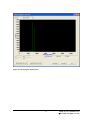
3.1 Overview
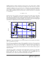
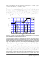
The Pixie-16 graphical user interface (Figure 3.1) provides the user a simple yet powerful
tool to control the Pixie-16 cards. It was written using Microsoft’s Visual Basic programming
language and its underlying function calls were directed to a dynamic link library (DLL),
Pixie16.dll. Those users who are interesting in learning more about this DLL can read the
Programmer’s Manual. The user interface consists of a work area where DAQ graphs, tables
and panels are to be shown, a column to the right which contains series of control buttons, a
message window, status indicators, control menus, and control icons.
Figure 3.1: The graphical user interface for Pixie-16.
6
PIXIE-16 User’s Manual V1.0.6
XIA 2005. All rights reserved.
We describe below the steps of using this user interface.
3.2 Configure and Boot Pixie-16 cards
After installing the Pixie-16 software on the user’s computer, the Pixie-16 user interface can
be launched by double clicking the executable file Pixie16_VB.exe in the installed folder.
The user will be given two operation modes to choose from: online or offline. In the online
mode, the user will be able to directly communicate to the Pixie-16 cards sitting in a PXI
chassis and all whistles and bells of the user interface will be accessible. In the offline mode
when no Pixie-16 cards are available for communication, the user can still access every
buttons or controls of the interface. In fact, a user can even launch a data acquisition run and
watch the run progress. However, data display is limited to the previously stored data files.
Figure 3.2: The operation mode selection panel.
After the user interface is launched, the user will see the operation mode selection panel as
shown in Figure 3.2. If the user chooses the online mode then saves this setting by clicking
the Save settings menu item, this panel will not show up anymore when the interface is
launched subsequently. In offline mode, this panel will always pop up whenever the interface
is started. The mode can also be switched by clicking Advanced -> Select Online/Offline
Mode or shortcut keys Ctrl+I.
Before starting up (booting) the Pixie-16 cards, the user should check the file paths and the
PXI slot settings. By clicking Files -> Boot files, the Boot Files panel (Figure 3.3) should
show up in the center of the work area and the user could choose the boot file paths and file
names. The user could directly input the file name in the boxes, or use the “file open” icon at
the right end of each line to locate a specific file. TIP: change the boot files path will
automatically change the file paths for all files.
7
PIXIE-16 User’s Manual V1.0.6
XIA 2005. All rights reserved.
Figure 3.3: The boot files selection panel.
As shown in Figure 3.4, the user can also check the mapping of Pixie-16 card number and the
corresponding slot number in a PXI chassis using the PXI Slots Setup panel. To add a Pixie16 card, enter a slot number in the box above the “Add” button then pressing “Add”.
Similarly, to delete a mapping, first select a slot number in the box underneath “Pixie-16 slot
number”, then press the “Remove” button.
The user should be ready by now to boot all Pixie-16 cards in the system by pressing the
button “Boot Pixie-16 Cards” on the Control Bar to the right. Messages printed out to the
Message Window should be checked to see if all cards have been started up successfully. If
one or more cards failed to boot, the user should check a message file called
“Pixie16msg.txt” for any causes leading to the failure. The message file is located in the
same folder as the user interface program Pixie16_VB.exe.
8
PIXIE-16 User’s Manual V1.0.6
XIA 2005. All rights reserved.
Figure 3.4: The PXI slot setup panel.
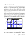
3.3 Check Integrity of Input Signals
Before starting a data acquisition run, the user can check if the detector signal inputs to the
Pixie-16 ADCs are normal in shape and are within the ranges of the ADCs. The Acquire
ADC Traces panel (Figure 3.5) is accessible through the button “Acquire ADC Traces” on
the Control Bar to the right. First select the Card and Channel number on the top of the
Control Bar, and then press the button “Acquire Trace” to get an un-triggered trace for the
selected channel. The signal is preferably to be at about 10% of the ADC range, i.e. the
baseline of the trace should be at around 400 ADC units. If not, change the DC-Offset then
press “Apply” which is next to the DC-Offset control. Then acquire another trace to see the
changed baseline level. Repeat this for other channels.
3.4 Acquire List Mode or Histogram Data
A user can start a list mode run by pressing the button “List Mode Run” on the Control Bar.
A message box will promptly pop up which shows the count-down of timeout. If the run can
not finish before the timeout kicks in, the run will be aborted. So depends on how fast the
Pixie-16 card buffer is expected to be filled, the user should set properly the Time Out for list
mode runs. In either case, i.e. the run finishing by itself and being aborted, list mode data
will be read out from the Pixie cards and saved to the list mode data file.
The user can also acquire MCA histogram data by starting a histogram run. To start a
histogram run, press the button “Histogram Run” on the Control Bar. A message box would
promptly pop up which shows the count-down of run time. After the run time expires, the
run will be stopped and histogram will be ready to be read out from the Pixie cards or saved
to the histogram data file.
9
PIXIE-16 User’s Manual V1.0.6
XIA 2005. All rights reserved.
Figure 3.5: The ADC Trace panel where un-triggered ADC traces can be acquired and shown.
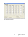
3.5 View Acquired Histogram or List Mode Data
A user can view acquired histogram or list mode data right after a histogram or list mode run
is finished. These data are accessible through Run Results -> MCA Histogram or Run Results
-> List Mode Traces. Alternatively, the user can also retrieve these data from stored data
files. This is useful for offline analysis of previously acquired histogram or list mode data.
Figure 3.6 shows the histogram spectrum display panel. A user can read out the histogram
either from the card (for on-line mode) or from a file (for off-line mode). By changing the
control “Chan #” on the right top corner of the main control window, the user can check the
histogram data channel by channel.
Figure 3.7 shows the list mode trace display panel. By changing the channel number in the
control “Select chan #”, the user can see totally how many events there are for the selected
channel, and be able to browse through these events one-by-one. The event energy calculated
by the Pixie-16 will also be shown.
10
PIXIE-16 User’s Manual V1.0.6
XIA 2005. All rights reserved.
Figure 3.6: The histogram display panel.
11
PIXIE-16 User’s Manual V1.0.6
XIA 2005. All rights reserved.
Figure 3.7: The list mode trace display panel.
3.6 Adjust DAQ Parameters
Pixie-16 users can also adjust certain DAQ parameters through the user interface. For list
mode runs (Figure 3.8), a user can change the trace acquisition settings, namely, the trace
length and trace delay for each channel. The user can also change the number of repeated
runs (number of spills), the run status polling interval and the time out control. For MCA
runs, the user can change the preset run time. In addition, a user can also change the DAQ
parameters (Figure 3.9), namely, the energy filter lengths, trigger filter lengths, and the
trigger threshold, and the preamplifier decay time, etc.
12
PIXIE-16 User’s Manual V1.0.6
XIA 2005. All rights reserved.
Figure 3.8: The list mode run parameters setup panel.
13
PIXIE-16 User’s Manual V1.0.6
XIA 2005. All rights reserved.
Figure 3.9: The channel parameters setup panel.
14
PIXIE-16 User’s Manual V1.0.6
XIA 2005. All rights reserved.
4 Data Runs and Data Structures
4.1
Run types
There are two run types: List mode runs and histogram runs. Histogram runs only collect
spectra; list mode runs acquire data on an event-by event basis.
4.1.1 Histogram Runs
If all you want to do is to collect spectra, runs should be started in histogram mode. For each
event, pulse heights are calculated and used to increment the spectrum for the corresponding
channel, then discarded. Runs can continue indefinitely, or until a preset time is reached.
Besides the spectrum, run statistics are available at the end of the run.
4.1.2 List Mode Runs
If, on the other hand, you want to collect data on an event-by-event basis, gathering energies,
time stamps, pulse shape analysis values, and waveforms, for each event, you should operate
the Pixie-16 in multi-parametric or list mode. In list mode, you still obtain histogramming of
energies, e.g. for monitoring purposes. Runs will continue until the output buffer is filled, or
a preset number of events is reached. The control software also includes a timeout feature,
causing the host to end runs that do not end themselves.
4.2
Output data structures
Output data are available in two different memory blocks. The multichannel analyser (MCA)
block resides in memory external to the DSP. The list mode data buffer is located in internal
DSP data memory and consists of 64K 32-bit words.
4.2.1 MCA histogram data
The MCA block is fixed to 32k words (32 bit) per channel, residing in the external memory.
The memory can be read out via the PCI data bus at rates over 100Mbyte/s and stored to file.
If spectra of less than 32k length are requested, only part of the 32k will be filled with data.
4.2.2 List mode data
The data of the output buffer is organized into one buffer header, an event header for each
captured event, and a channel header followed by waveform data for each active channel
included in the event. All header information consists of 32-bit data words. Waveform data
consists of two samples of 16-bit trace data combined into one 32 bit word.
The list mode data in the linear output data buffer can be written in a number of formats.
User code should access the three variables BUFHEADLEN, EVENTHEADLEN, and
15
PIXIE-16 User’s Manual V1.0.6
XIA 2005. All rights reserved.
CHANHEADLEN in the configuration file of a particular run to navigate through the data
set.
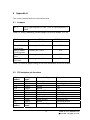
The buffer content always starts with a buffer header of length BUFHEADLEN. Currently,
BUFHEADLEN is six, and the six words are:
32-bit Word #
1
2
3
4
5
6
Variable
BUF_NDATA
BUF_MODNUM
BUF_FORMAT
BUF_TIMEHI
BUF_TIMEMI
BUF_TIMELO
Description
Number of words in this buffer
Module number
Run type
Run start time, high word
Run start time, middle word
Run start time, low word
Table 4.1: Buffer header data format.
Following the buffer header, the events are stored in sequential order. Each event starts out
with an event header of length EVENTHEADLEN. Currently, EVENTHEADLEN=3, and
the three words are:
32-bit Word #
1
2
3
Name
EVT_PATTERN
EVT_TIMEHI
EVT_TIMELO
Description
Hit pattern
Event arrival time, high word
Event arrival time, low word
Table 4.2: Event header data format.
The hit pattern is a bit mask, which tells which channels were read out. The LSB (bit 0), if
set, indicates that channel 0 has been read. Bit number n, if set, indicates that channel n has
been read. The bits set, 0…15, tells for which channels data have been recorded following
the event header. After the event header there follow the channel information as indicated by
the hit pattern, and in order of increasing channel numbers.
The data for each channel are organized into a channel header of length CHANHEADLEN,
which may be followed by waveform data. CHANHEADLEN depends on the run type and
on the method of data buffering. Currently, the following data formats are used:
1.
For List Mode, CHANHEADLEN=9, and the nine words are
32-bit Word #
1
2
3
4
5
Name
CHAN_NDATA
CHAN_TRIGTIME
CHAN_ENERGY
CHAN_TOUT
CHAN_LOUT
Description
Number of 32-bit words for this channel
Fast trigger time
Energy
Energy filter trailing sum for debug
Energy filter leading sum for debug
16
PIXIE-16 User’s Manual V1.0.6
XIA 2005. All rights reserved.
6
7
8
9
CHAN_GOUT
Reserved
Reserved
Reserved
Energy filter gap sum for debug
Table 4.3: Channel header, possibly followed by waveform data.
Any waveform data for this channel would then follow this header. An offline analysis
program can recognize this by computing N_WAVE_DATA=CHAN_DATA-9. If
N_WAVE_DATA is greater than zero, it indicates the number of 32-bit waveform data
words to follow. In each 32-bit word of the waveform data, two samples of 16-bit trace data
are stored. The earlier sample is stored in the lower 16 bit:
32-bit Word #
1
2
3
4
…
lower 16 bit
trace data 0
trace data 2
trace data 4
trace data 6
…
higher 16 bit
trace data 1
trace data 3
trace data 5
trace data 7
…
Table 4.4: Waveform data packing into 32 bit.
NOTE: Always set the Trace Length to be even multipliers of 0.01 µs. For example, use
10.22µs, not 10.21 µs.
17
PIXIE-16 User’s Manual V1.0.6
XIA 2005. All rights reserved.
5 Hardware Description
The Pixie-16 is a 16-channel unit designed for gamma-ray spectroscopy and waveform
capturing. It incorporates five functional building blocks, which we describe below. This
section concentrates on the functionality aspect. Technical specification can be found in
section 1.2.
5.1
Analog signal conditioning
Each analog input has its own signal conditioning unit. The task of this circuitry is to adapt
the incoming signals to the ADC.
Input signals are amplified and adjusted for offsets using a DAC programmed by the host.
This will bring the signals into the ADC's voltage range of 2V. The ADC is not a peak
sensing ADC, but acts as a waveform digitizer. In order to avoid aliasing, we remove the
high frequency components from the incoming signal prior to feeding it into the ADC. The
anti-aliasing filter, an active Sallen-Key filter, cuts off sharply at the Nyquist frequency,
namely half the ADC sampling frequency.
Though the Pixie-16 can work with many different signal forms, best performance is to be
expected when sending the output from a charge integrating preamplifier directly to the
Pixie-16 without any further shaping.
5.2
Real-time processing units
The real time processing units (RTPUs), one per four input channels, consist of a field
programmable gate array (FPGA) also incorporating a FIFO memory for each channel. The
data stream from the ADCs is sent to these units at the full ADC sampling rate. Using a
pipelined architecture, the signals are also processed at this high rate, without the help of the
on-board digital signal processor (DSP).
Note that the use of one RTPU for four channels allows sampling the incoming signal at four
times the regular ADC clock frequency. If the channels are fed the same input signal, the
RTPU can give the each ADC a clock with a 90 degree phase shift, thus sampling the signal
four times in one clock cycle. Special software is required to combine the input streams into
one; contact XIA for details.
The real-time processing units apply digital filtering to perform essentially the same action as
a shaping amplifier. The important difference is in the type of filter used. In a digital
application it is easy to implement finite impulse response filters, and we use a trapezoidal
filter. The flat top will typically cover the rise time of the incoming signal and makes the
pulse height measurement less sensitive to variations of the signal shape.
18
PIXIE-16 User’s Manual V1.0.6
XIA 2005. All rights reserved.
Secondly, the RTPUs contain a pileup inspector. This logic ensures that if a second pulse is
detected too soon after the first, so that it would corrupt the first pulse height measurement,
both pulses are rejected as piled up. The pileup inspector is, however, not very effective in
detecting pulse pileup on the rising edge of the first pulse, i.e. in general pulses must be
separated by their rise time to be effectively recognized as different pulses. Therefore, for
high count rate applications, the pulse rise times should be as short as possible, to minimize
the occurrence of pileup peaks in the resulting spectra.
If a pulse was detected and passed the pileup inspector, a trigger may be issued. That trigger
would notify the DSP that there are raw data available now. If a trigger was issued the data
remain latched until the RTPU has been serviced by the DSP.
The third component of the RTPU is a FIFO memory, which is controlled by the pileup
inspector logic. The FIFO memory is continuously being filled with waveform data from the
ADC. On a trigger it is stopped, and the read pointer is positioned such that it points to the
beginning of the pulse that caused the trigger. When the DSP collects event data, it can read
any fraction of the stored waveform, up to the full length of the FIFO.
5.3
Digital signal processor (DSP)
The DSP controls the operation of the Pixie-16, reads raw data from the RTPUs, reconstructs
true pulse heights, applies time stamps, prepares data for output to the host computer, and
increments spectra in the on-board memory.
The host computer communicates with the DSP, via the PCI interface, using a direct memory
access (DMA) channel. Reading and writing data to DSP memory does not interrupt its
operation, and can occur even while a measurement is underway.
The host sets variables in the DSP memory and then calls DSP functions to program the
hardware. Through this mechanism all offset DACs are set and the RTPUs are programmed
with their filter parameters.
The RTPUs process their data without support from the DSP, once they have been set up.
When any one or more of them generate a trigger, an interrupt request is sent to the DSP. It
responds with reading the required data from the RTPUs and storing those in memory. It then
returns from the interrupt routine without processing the data to minimize the DSP induced
dead time. The event processing routine works from the data in memory to generate the
requested output data.
In this scheme, the greatest processing power is located in the RTPUs. Implemented in
FPGAs each of them processes the incoming waveforms from its associated ADC in real
time and produces, for each valid a event, a small set of distilled data from which pulse
heights and arrival times can be reconstructed. The computational load for the DSP is much
reduced, as it has to react only on an event-by-event basis and has to work with only a small
set of numbers for each event.
19
PIXIE-16 User’s Manual V1.0.6
XIA 2005. All rights reserved.
5.4
PCI interface
The PCI interface through which the host communicates with the Pixie-16 is implemented in
a PCI slave IC together with an FPGA. The configuration of this PCI IC is stored in a
PROM, which is placed in the only DIP-8 IC-socket on the Pixie-16 board. The interface
conforms to the commercial PCI standard. It moves 32-bit data words at a time.
The interface dos not issue interrupt requests to the host computer. Instead, for example to
determine when data is ready for readout, the host has to poll a Control and Status Register
(CSR) in the Communication FPGA.
The Communication FPGA links the PCI slave with the DSP and the on-board memory. The
host can read out the memory without interrupting the operation of the DSP. This allows
updates of the MCA spectrum while a run is in progress.
5.5
Trigger Interface
A further FPGA acts as an interface between the DSP, Signal Processing FPGAs and the
backplane. Some basic trigger distribution is implemented in the Communication FPGA. The
Trigger FPGA has many more backplane lines for extended trigger distribution, and has 18
general purpose I/O connections available on the front panel.
It can be configured to receive trigger and hit pattern information from the Signal Processing
FPGAs, and pass it on through the backplane to other Pixie-16 modules. In this way,
coincidence or multiplicity decisions can be made to accept or not accept an event; or a cell
in a 2D array can trigger its neighboring cells.
The DSP can also send and receive data through a link port through the Trigger FPGA and
the backplane to and from other DSPs in the system.
The Trigger FPGA can be configured depending on the specific application. Currently no
default configuration is implemented. Contact XIA if you want to make use on any of the
extended trigger distribution possibilities.
20
PIXIE-16 User’s Manual V1.0.6
XIA 2005. All rights reserved.
6 Theory of Operation
6.1
Digital Filters for γ-ray detectors
Energy dispersive detectors, which include such solid state detectors as Si(Li), HPGe, HgI2,
CdTe and CZT detectors, are generally operated with charge sensitive preamplifiers as
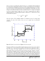
shown in Figure 6.1 a). Here the detector D is biased by voltage source V and connected to
the input of preamplifier A which has feedback capacitor Cf and feedback resistor Rf.
The output of the preamplifier following the absorption of an γ-ray of energy Ex in detector D
is shown in Figure 6.1 b) as a step of amplitude Vx (on a longer time scale, the step will
decay exponentially back to the baseline, see section 6.3). When the γ-ray is absorbed in the
detector material it releases an electric charge Qx = Ex/ε, where ε is a material constant. Qx is
integrated onto Cf, to produce the voltage Vx = Qx/Cf = Ex/(εCf). Measuring the energy Ex of
the γ-ray therefore requires a measurement of the voltage step Vx in the presence of the
amplifier noise σ, as indicated in Figure 6.1 b).
Rf
V
Cf
D
A
Preamp Output (mV)
4
2
σ
-2
-4
0.00
a)
Vx
0
b)
0.02
0.04
0.06
Time (ms)
Figure 6.1: a) Charge sensitive preamplifier with RC feedback; b) Output on absorption of an
γ-ray.
Reducing noise in an electrical measurement is accomplished by filtering. Traditional analog
filters use combinations of a differentiation stage and multiple integration stages to convert
the preamp output steps, such as shown in Figure 6.1 b), into either triangular or semiGaussian pulses whose amplitudes (with respect to their baselines) are then proportional to
Vx and thus to the γ-ray’s energy.
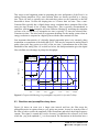
Digital filtering proceeds from a slightly different perspective. Here the signal has been
digitized and is no longer continuous. Instead it is a string of discrete values as shown in
21
PIXIE-16 User’s Manual V1.0.6
XIA 2005. All rights reserved.
Figure 6.2. Figure 6.2 is actually just a subset of Figure 6.1 b), in which the signal was digitized
by a Tektronix 544 TDS digital oscilloscope at 10 MSA (megasamples/sec). Given this data
set, and some kind of arithmetic processor, the obvious approach to determining Vx is to take
some sort of average over the points before the step and subtract it from the value of the
average over the points after the step. That is, as shown in Figure 6.2, averages are computed
over the two regions marked “Length” (the “Gap” region is omitted because the signal is
changing rapidly here), and their difference taken as a measure of Vx. Thus the value Vx may
be found from the equation:
V x ,k = −
∑
WiVi +
i ( before )
∑W V
i
(1)
i
i ( after )
where the values of the weighting constants Wi determine the type of average being
computed. The sums of the values of the two sets of weights must be individually
normalized.
Preamp Output (mV)
4
2
Length
Gap
0
Length
-2
-4
20
22
24
26
28
30
Time ( µs)
Figure 6.2: Digitized version of the data of Figure 6.1 b) in the step region.
The primary differences between different digital signal processors lie in two areas: what set
of weights { Wi } is used and how the regions are selected for the computation of Eqn. 1.
Thus, for example, when larger weighting values are used for the region close to the step
while smaller values are used for the data away from the step, Eqn. 1 produces “cusp-like”
filters. When the weighting values are constant, one obtains triangular (if the gap is zero) or
trapezoidal filters. The concept behind cusp-like filters is that, since the points nearest the
step carry the most information about its height, they should be most strongly weighted in the
averaging process. How one chooses the filter lengths results in time variant (the lengths vary
22
PIXIE-16 User’s Manual V1.0.6
XIA 2005. All rights reserved.
from pulse to pulse) or time invariant (the lengths are the same for all pulses) filters.
Traditional analog filters are time invariant. The concept behind time variant filters is that,
since the γ-rays arrive randomly and the lengths between them vary accordingly, one can
make maximum use of the available information by setting the length to the interpulse
spacing.
In principal, the very best filtering is accomplished by using cusp-like weights and time
variant filter length selection. There are serious costs associated with this approach however,
both in terms of computational power required to evaluate the sums in real time and in the
complexity of the electronics required to generate (usually from stored coefficients)
normalized { Wi } sets on a pulse by pulse basis.
The Pixie-16 takes a different approach because it was optimized for very high speed
operation. It implements a fixed length filter with all Wi values equal to unity and in fact
computes this sum afresh for each new signal value k. Thus the equation implemented is:
LV x ,k = −
k − L −G
∑Vi +
k
∑V
i = k − 2 L −G +1 i = k − L +1
i
(2)
where the filter length is L and the gap is G . The factor L multiplying Vx ,k arises because
the sum of the weights here is not normalized. Accommodating this factor is trivial.
While this relationship is very simple, it is still very effective. In the first place, this is the
digital equivalent of triangular (or trapezoidal if G ≠ 0) filtering which is the analog
industry’s standard for high rate processing. In the second place, one can show theoretically
that if the noise in the signal is white (i.e. Gaussian distributed) above and below the step,
which is typically the case for the short shaping times used for high signal rate processing,
then the average in Eqn. 2 actually gives the best estimate of Vx in the least squares sense.
This, of course, is why triangular filtering has been preferred at high rates. Triangular
filtering with time variant filter lengths can, in principle, achieve both somewhat superior
resolution and higher throughputs but comes at the cost of a significantly more complex
circuit and a rate dependent resolution, which is unacceptable for many types of precise
analysis. In practice, XIA’s design has been found to duplicate the energy resolution of the
best analog shapers while approximately doubling their throughput, providing experimental
confirmation of the validity of the approach.
6.2
Trapezoidal Filtering in the Pixie-16
From this point onward, we will only consider trapezoidal filtering as it is implemented in the
Pixie-16 according to Eqn. 2. The result of applying such a filter with Length L=1µs and Gap
G=0.4µs to a γ-ray event is shown in Figure 6.3. The filter output is clearly trapezoidal in
shape and has a rise time equal to L, a flattop equal to G, and a symmetrical fall time equal to
L. The basewidth, which is a first-order measure of the filter’s noise reduction properties, is
thus 2L+G.
23
PIXIE-16 User’s Manual V1.0.6
XIA 2005. All rights reserved.
This raises several important points in comparing the noise performance of the Pixie-16 to
analog filtering amplifiers. First, semi-Gaussian filters are usually specified by a shaping
time. Their rise time is typically twice this and their pulses are not symmetric so that the
basewidth is about 5.6 times the shaping time or 2.8 times their rise time. Thus a semiGaussian filter typically has a slightly better energy resolution than a triangular filter of the
same rise time because it has a longer filtering time. This is typically accommodated in
amplifiers offering both triangular and semi-Gaussian filtering by stretching the triangular
rise time a bit, so that the true triangular rise time is typically 1.2 times the selected semiGaussian rise time. This also leads to an apparent advantage for the analog system when its
energy resolution is compared to a digital system with the same nominal rise time.
One important characteristic of a digitally shaped trapezoidal pulse is its extremely sharp
termination on completion of the basewidth 2L+G. This may be compared to analog filtered
pulses whose tails may persist up to 40% of the rise time, a phenomenon due to the finite
bandwidth of the analog filter. As we shall see below, this sharp termination gives the digital
filter a definite rate advantage in pileup free throughput.
ADC output
Filter Output
3
ADC units
33x10
32
31
G
L
2L+G
30
9.5
10.0
10.5
11.0
Time
11.5
12.0
12.5µs
Figure 6.3: Trapezoidal filtering of a preamplifier step with L=1µs and G=0.4µs.
6.3
Baselines and preamplifier decay times
Figure 6.4 shows an event over a longer time interval and how the filter treats the
preamplifier noise in regions when no γ-ray pulses are present. As may be seen the effect of
the filter is both to reduce the amplitude of the fluctuations and reduce their high frequency
content. This signal is termed the baseline because it establishes the reference level from
which the γ-ray peak amplitude Vx is to be measured The fluctuations in the baseline have a
24
PIXIE-16 User’s Manual V1.0.6
XIA 2005. All rights reserved.
standard deviation σe which is referred to as the electronic noise of the system, a number
which depends on the rise time of the filter used. Riding on top of this noise, the γ-ray peaks
contribute an additional noise term, the Fano noise, which arises from statistical fluctuations
in the amount of charge Qx produced when the γ-ray is absorbed in the detector. This Fano
noise σf adds in quadrature with the electronic noise, so that the total noise σt in measuring
Vx is found from
σt = sqrt( σf2 + σe2)
(3)
The Fano noise is only a property of the detector material. The electronic noise, on the other
hand, may have contributions from both the preamplifier and the amplifier. When the
preamplifier and amplifier are both well designed and well matched, however, the amplifier’s
noise contribution should be essentially negligible. Achieving this in the mixed analog-digital
environment of a digital pulse processor is a non-trivial task, however.
3
33x10
σt
32
ADC units
ADC Output
Filter Output
31
30
Vx
σe
29
28
75
80
85
90
95µs
Time
Figure 6.4: A γ-ray event displayed over a longer time period to show baseline noise and the
effect of preamplifier decay time.
With a RC-type preamplifier, the slope of the preamplifier is rarely zero. Every step decays
exponentially back to the DC level of the preamplifier. During such a decay, the baselines are
obviously not zero. This can be seen in Figure 6.4, where the filter output during the
exponential decay after the pulse is below the initial level. Note also that the flat top region is
sloped downwards.
Using the decay constant τ, the baselines can be mapped back to the DC level. This allows
precise determination of γ-ray energies, even if the pulse sits on the falling slope of a
previous pulse. The value of τ, being a characteristic of the preamplifier, has to be
determined by the user and host software and downloaded to the module.
25
PIXIE-16 User’s Manual V1.0.6
XIA 2005. All rights reserved.
6.4
Thresholds and Pile-up Inspection
As noted above, we wish to capture a value of Vx for each γ-ray detected and use these values
to construct a spectrum. This process is also significantly different between digital and
analog systems. In the analog system the peak value must be “captured” into an analog
storage device, usually a capacitor, and “held” until it is digitized. Then the digital value is
used to update a memory location to build the desired spectrum. During this analog to digital
conversion process the system is dead to other events, which can severely reduce system
throughput. Even single channel analyzer systems introduce significant deadtime at this stage
since they must wait some period (typically a few microseconds) to determine whether or not
the window condition is satisfied.
Digital systems are much more efficient in this regard, since the values output by the filter
are already digital values. All that is required is to take the filter sums, reconstruct the energy
Vx, and add it to the spectrum. In the Pixie-16, the filter sums are continuously updated by
the RTPU (see section 5.2), and only have to be read out by the DSP when an event occurs.
Reconstructing the energy and incrementing the spectrum is done by the DSP, so that the
RTPU is ready to take new data immediately after the readout. This usually takes much less
than one filter rise time, so that no system deadtime is produced by a “capture and store”
operation. This is a significant source of the enhanced throughput found in digital systems.
3
32x10
ADC Output
Fast Filter Output
Slow Filter Output
31
ADC units
30
29
28
Sampling Time
Arrival Time
27
Threshold
26
44
45
46
47
48µs
Time
Figure 6.5: Peak detection and sampling in the Pixie-16.
The peak detection and sampling in the Pixie-16 is handled as indicated in Figure 6.5. Two
trapezoidal filters are implemented, a fast filter and a slow filter. The fast filter is used to
detect the arrival of γ-rays, the slow filter is used for the measurement of Vx, with reduced
26
PIXIE-16 User’s Manual V1.0.6
XIA 2005. All rights reserved.
noise at longer filter rise times. The fast filter has a filter length Lf = 0.1µs and a gap Gf
=0.1µs. The slow filter has Ls = 1.2µs and Gs = 0.35µs.
The arrival of the γ-ray step (in the preamplifier output) is detected by digitally comparing
the fast filter output to THRESHOLD, a digital constant set by the user. Crossing the
threshold starts a counter to count PEAKSAMP clock cycles to arrive at the appropriate time
to sample the value of the slow filter. Because the digital filtering processes are deterministic,
PEAKSAMP depends only on the values of the fast and slow filter constants and the rise
time of the preamplifier pulses. The slow filter value captured following PEAKSAMP is then
the slow digital filter’s estimate of Vx.
3
36x10
3
34
2
1
32
ADC units
ADC Output
30
28
26
24
Slow Filter Output
22
Fast Filter Output
PeakSep
20
56
58
60
62
Time
64
66
68µs
Figure 6.6: A sequence of 3 γ-ray pulses separated by various intervals to show the origin of
pileup and demonstrate how it is detected by the Pixie-16.
The value Vx captured will only be a valid measure of the associated γ-ray’s energy provided
that the filtered pulse is sufficiently well separated in time from its preceding and succeeding
neighbor pulses so that their peak amplitudes are not distorted by the action of the trapezoidal
filter. That is, if the pulse is not piled up. The relevant issues may be understood by reference
to Figure 6.6, which shows 3 γ-rays arriving separated by various intervals. The fast filter has
a filter length Lf = 0.1µs and a gap Gf =0.1µs. The slow filter has Ls = 1.2µs and Gs = 0.35µs.
Because the trapezoidal filter is a linear filter, its output for a series of pulses is the linear
sum of its outputs for the individual members in the series. Pileup occurs when the rising
edge of one pulse lies under the peak (specifically the sampling point) of its neighbor. Thus,
in Figure 6.6, peaks 1 and 2 are sufficiently well separated so that the leading edge of peak 2
falls after the peak of pulse 1. Because the trapezoidal filter function is symmetrical, this also
means that pulse 1’s trailing edge also does not fall under the peak of pulse 2. For this to be
true, the two pulses must be separated by at least an interval of L + G. Peaks 2 and 3, which
27
PIXIE-16 User’s Manual V1.0.6
XIA 2005. All rights reserved.
are separated by less than 1.0 µs, are thus seen to pileup in the present example with a 1.2 µs
rise time.
This leads to an important point: whether pulses suffer slow pileup depends critically on the
rise time of the filter being used. The amount of pileup which occurs at a given average
signal rate will increase with longer rise times.
Because the fast filter rise time is only 0.1 µs, these γ-ray pulses do not pileup in the fast
filter channel. The Pixie-16 can therefore test for slow channel pileup by measuring the fast
filter for the interval PEAKSEP after a pulse arrival time. If no second pulse occurs in this
interval, then there is no trailing edge pileup. PEAKSEP is usually set to a value close to L +
G + 1. Pulse 1 passes this test, as shown in Figure 6.6. Pulse 2, however, fails the PEAKSEP
test because pulse 3 follows less than 1.0 µs. Notice, by the symmetry of the trapezoidal
filter, if pulse 2 is rejected because of pulse 3, then pulse 3 is similarly rejected because of
pulse 2.
6.5
Filter range
To accommodate the wide range of filter rise times from 0.04 µs to 81 µs, the filters are
implemented in the RTPUs configurations with different clock decimation (filter ranges).
The ADC sampling rate is always 10ns, but in higher clock decimations, several ADC
samples are averaged before entering the filtering logic. In decimation 1, 21 samples are
averaged, 22 samples in decimation 2, and so on. Since the sum of rise time and flat top is
limited to 127 decimated clock cycles, filter time granularity and filter times are limited to
the values are listed in Table 6.1.
Filter range
1
2
3
4
5
6
Filter granularity
0.02µs
0.04µs
0.08µs
0.16µs
0.32µs
0.64µs
max. Trise+Tflat
2.54µs
5.08µs
10.16µs
20.32µs
40.64µs
81.28µs
min. Trise
0.04µs
0.08µs
0.16µs
0.32µs
0.64µs
1.28µs
min. Tflat
0.06µs
0.12µs
0.24µs
0.48µs
0.96µs
1.92µs
Table 6.1: RTPU clock decimations and filter time granularity.
All filter ranges are implemented in the same FPGA configuration. Only the “Filter Range”
parameter of the DSP has to be set to select a particular range.
28
PIXIE-16 User’s Manual V1.0.6
XIA 2005. All rights reserved.
7 Operating multiple Pixie-16 modules synchronously
When many Pixie-16 modules are operating as a system, it may be required to synchronize
clocks and timers between them and to distribute triggers across modules. It will also be
necessary to ensure that runs are started and stopped synchronously in all modules. All these
signals are distributed through the PXI backplane.
7.1
Clock distribution
In a multi-module system there will be one clock master and a number of clock slaves or
repeaters. The clock function of a module can be selected by setting shunts on Jumper JP101
at the rear of the board.
Pins 3 and 4 are the input to the board’s clock distribution circuitry. They can be connected
with a shunt to one of the other pins, thus choosing a particular clock distribution mode.
BUS
Left
LOC
a) Individual or
clock master
mode
BUS
PXI
LOC
BUS
b) Clock
repeater mode
Left
PXI
JP101
PXI
JP101
Left
JP101
PXI
JP101
Left
LOC
c) Bussed clock
slave mode
BUS
LOC
d) PXI clock
slave mode
Figure 7.1: Jumper Settings for different clock distribution modes. In a group of modules,
there will be one daisy-chained clock master (a) in the leftmost position and several
repeaters (b). If there is a source for the bussed backplane clock, the modules can also be
configured as bus clock slave (c). If the usual 10MHz PXI clock from the backplane is
overridden with a 50 MHz clock, the modules can be configured as PXI clock slaves (d).
7.1.1 Individual Clock mode
If only one Pixie-16 module is used in the system, or if clocks between modules do not have
to be synchronized, the module should be set into individual clock mode, as shown in Figure
7.1a. Connect pin 3 of JP101 (the clock input) with a shunt to pin 5, which is labeled “LOC”.
This will use the local clock crystal as the clock source.
29
PIXIE-16 User’s Manual V1.0.6
XIA 2005. All rights reserved.
7.1.2 Daisy-chained Clock Mode
The preferred way to distribute clocks between modules is to daisy-chain the clocks from
module to module, where each module repeats and amplifies the signal. This requires one
master module, located in the leftmost slot of the group of Pixie-16 modules. The master
module has the same jumper settings as an individual module, see Figure 7.1a. Configure the
other modules in the chassis as clock repeaters by setting the jumpers as shown in Figure
7.1b; i.e. connect pin 4 of JP101 with a shunt to pin 2, which is labeled “Left”. This will use
the clock signal from the left neighbor as the clock source. The must be no gaps between
modules.
Note that the clock output to the right neighbor is always enabled, i.e. every board,
independent of its clock mode, sends out a clock to its right neighbor its as long as it has a
clock itself.
7.1.3 Bussed Clock Mode
If there have to be gaps between a group of Pixie-16 modules, the daisy-chained clock
distribution will not work since the chain is broken. In this case, the modules can be
configured for bussed clock mode, where a clock signal is distributed through the backplane
to all modules. A separate clock master module, such as XIA’s PDM power and trigger
module, has to be used as the clock master. The drive strength of the clock master usually
limits the number of slaves to 3-4 modules.
To configure a Pixie-16 module as the bussed clock slave modules, place a shunt on JP101 as
shown in Figure 7.1c, i.e. set one shunt to connect pins 4 and 6 (“BUS”).
Note that the bussed clock line does usually not connect over a PCI bridge in chassis with
more than 8 slots, whereas daisy-chains usually do.
7.1.4 PXI Clock Mode
A further option for clock distribution is to use the PXI clock distributed on the backplane,
by connecting pin 1 and 3 on JP101 (“PXI”), as shown in Figure 7.1d. By default, this line is
driven by the PXI backplane at a rate of 10 MHz - too slow to run the Pixie-16 modules.
Only if a custom backplane provides 50 MHz, or if a custom module (such as XIA’s PDM
power and trigger module) in slot 2 overrides the default signal from the backplane, can this
input be used as an alternative setting for clock slaves.
7.2
Trigger distribution
Two kinds of standard triggers can be distributed over the PXI backplane: Fast triggers and
event triggers. Fast triggers are generated when the fast filter goes above threshold as
described in section 6.4. Event triggers are generated if no pile up is detected in the
PEAKSEP interval after the fast trigger; they essentially act as trigger validation.
30
PIXIE-16 User’s Manual V1.0.6
XIA 2005. All rights reserved.
Both triggers are distributed over the PXI backplane as a wired-OR bussed signal. Normally
pulled high, the signal is driven low by the module that issues a trigger. All other modules
detect the line being low and use the fast trigger to stop the waveform acquisition in the
FIFO, or use the event trigger validate data for read. The reaction to distributed triggers has
to be enabled in the software.
Note that for the trigger timing to be correct, all modules and channels in a trigger group
should be set to the same energy filter peaking time and gap time.
Beside the standard trigger signals, there are more than 160 lines on the custom backplane to
distribute trigger, coincidence and I/O signals. These can be configured in a number of ways.
Contact XIA for customizing these lines.
7.3
Run Synchronization
It is possible to make all Pixie-16 modules in a system start and stop runs at the same time by
using a wired-OR SYNC line on the PXI backplane. In all modules the DSP variable
SYNCHWAIT has to be set to 1. If the run synchronization is not used SYNCHWAIT must
be set to 0.
The run synchronization works as follows. When the host computer requests a run start, the
DSP will first execute a run initialization sequence (clearing memory etc). At the beginning
of the run initialization the DSP causes the SYNC line to be driven low. At the end of the
initialization, the DSP enters a waiting loop, and allows the SYNC line to be pulled high by
pullup resistors. As long as at least one of all modules is still in the initialization, the SYNC
line will be low. When all modules are done with the initialization and waiting loop, the
SYNC line will go high. The low->high transition will signal the DSP to break out of the
loop and begin taking data.
If the timers in all modules are to be synchronized at this point, set the variable INSYNCH to
0. This instructs the DSP to reset all timers to zero when coming out of the waiting loop.
From then on they will remain in synch if the system is operated from one master clock.
Whenever a module encounters an end-of-run condition and stops the run it will also drive
the SYNC line low. This will be detected in all other modules, and in turn stop their data
acquisition.
Note that if the run synchronization is not operating properly and there was a run start request
with SYNCHWAIT=1, the DSP will be caught in an infinite loop. This can be recognized by
reading the variables INSYNCH and SYNCHWAIT. If after the run start request the DSP
continues to show INSYNCH=0 and SYNCHWAIT=1, it is stuck in the loop waiting for an
OK to begin the run. Besides rebooting, there is a software way to force the DSP to exit from
that loop and to lead it back to regular operation. See the Programmer’s Manual for details.
31
PIXIE-16 User’s Manual V1.0.6
XIA 2005. All rights reserved.
7.4
External gate — GFLT (Veto)
It is common in larger applications to have dedicated electronics to create event triggers or
vetoes. While the Pixie-16 does not accept an external fast trigger, it does accept a global
first level trigger (GFLT). This signal acts as a validation for an event already recognized by
the Pixie-16. Based on multiplicities and other information the dedicated trigger logic needs
to make the decision whether to accept or reject a given event. If that decision can be made
within a filter peaking time of all Pixie-16 channels involved, then the GFLT input can be
used. The GFLT signal applied to the Pixie-16 must be logic 1 at the time when the event
data are latched in the RTPUs. This happens not before a filter rise time has passed since the
event arrival and not later than a rise time plus the flat top. Therefore the trigger logic should
generate a GFLT pulse that is logic 1 during the filter flat top.
The GFLT signal is distributed through the PXI backplane. Using XIA’s PDM module or a
custom board, external signals can be connected to the backplane. The front panel I/O
connections on the Pixie-16 can also be configured to bring in the GFLT signal to the
backplane.
Each involved channel can be programmed individually to require the presence of a GFLT in
order to latch event data.
32
PIXIE-16 User’s Manual V1.0.6
XIA 2005. All rights reserved.
8 Troubleshooting
8.1 Startup Problems
The following describes solutions to common startup problems.
1. Computer does not boot when Pixie module is installed in chassis
This is usually caused by an incorrect clock setting on the Pixie module. The module
needs to have a valid clock to respond to the computer’s scanning of the PCI bus.
2. Computer reports new hardware found, needs driver files
Whenever a Pixie module is installed in a slot of the chassis for the first time, it is
detected as new hardware, even if Pixie modules have been installed in other slots
previously. Point Windows to the driver files provided with the software distribution.
3. When starting up modules in the interface program, downloads are
”unsuccessful”
This can have a number of reasons. Verify that:
- The files and paths point to valid locations.
- The slot numbers entered match the location of the modules.
33
PIXIE-16 User’s Manual V1.0.6
XIA 2005. All rights reserved.
9 Appendix A
This section contains hardware-related information.
9.1
Jumpers
JP1_x
Set for input impedance of 50Ω. If not set, input impedance is
10KΩ.
Table 9.1: Analog conditioning selection jumpers on Pixie-16 modules. (x=1..16)
Module
Single Module
JP101
Connect pins 3 and 5
PCB Reference
LOC
Daisy-Chained
Clock Master
Daisy-Chained
Clock Repeater
Bussed Clock
Slave
Clock Slave with
PXI clock
Connect pins 3 and 5
LOC
Connect pins 2 and 4
Left
Connect pins 4 and 6
BUS
Connect pins 1 and 3
PXI
Table 9.2: On-board jumper settings for the clock distribution on Pixie-16 modules.
9.2
PXI backplane pin functions
J2 pin
number
1A
16A
17A
18A
21A
16B
18B
1C
3C
18C
J2 pin
number
PXI pin
name
LBL9
TRIG1
TRIG2
TRIG3
LBR0
TRIG0
TRIG4
LBL10
LBR8
TRIG5
PXI pin
name
Connection Type
Pixie pin function
Left neighbor
Bussed
Bussed
Bussed
Right neighbor
Bussed
Bussed
Left neighbor
Right neighbor
Bussed
Connection Type
Nearest Neighbor 0 (left)
Event Trigger
Veto
Sync
Clock output
Fast Trigger
Reserved
Nearest Neighbor 1 (left)
Token Ring Out
Token Ring Return
Pixie pin function
34
PIXIE-16 User’s Manual V1.0.6
XIA 2005. All rights reserved.
20C
3D
17D
2E
3E
16E
17E
LBL0
LBR9
STAR
LBL8
LBR10
TRIG7
CLK10
Left neighbor
Right neighbor
Star trigger to slot 2
Left neighbor
Right neighbor
Bussed
Clock
Clock input
Nearest Neighbor 0 (right)
Reserved
Token Ring In
Nearest Neighbor 1 (right)
Bussed Clock
PXI Clock
Table 9.3: Pins of the J2 backplane connector defined in the PXI standard used by the Pixie-16. Pins not
listed are not connected except for pull-ups recommended by the PXI standard.
35
PIXIE-16 User’s Manual V1.0.6
XIA 2005. All rights reserved.