1
User's Manual
Digital Gamma Finder (DGF)
Pixie-500 Express
Version 3.20, July 2014
XIA LLC
31057 Genstar Road
Hayward, CA 94544 USA
Phone: (510) 401-5760; Fax: (510) 401-5761
http://www.xia.com
Disclaimer
Information furnished by XIA is believed to be accurate and reliable. However, XIA assumes
no responsibility for its use, or for any infringement of patents, or other rights of third parties,
which may result from its use. No license is granted by implication or otherwise under the
patent rights of XIA. XIA reserves the right to change the DGF product, its documentation,
and the supporting software without prior notice.
Table of Contents
1 Overview..................................................................................................................................................3
1.1 Features.............................................................................................................................................3
1.2 Specifications....................................................................................................................................4
2 Setting Up.................................................................................................................................................5
2.1 Installation.........................................................................................................................................5
2.2 Getting Started...................................................................................................................................6
3 Navigating the Pixie Viewer...................................................................................................................10
3.1 Overview.........................................................................................................................................10
3.2 Setup Group.....................................................................................................................................11
3.3 Run Control Group..........................................................................................................................16
3.4 Results Group..................................................................................................................................16
3.5 Optimizing Parameters....................................................................................................................18
3.6 File Series........................................................................................................................................20
4 Data Runs and Data Structures...............................................................................................................24
4.1 Run Types.......................................................................................................................................24
4.2 Output Data Structures....................................................................................................................25
5 Hardware Description.............................................................................................................................28
5.1 Analog Signal Conditioning............................................................................................................28
5.2 Pulse Processing..............................................................................................................................29
5.3 Digital Signal Processor (DSP) and Event Building........................................................................30
5.4 PCI Express Interface......................................................................................................................30
6 Theory of Operation...............................................................................................................................31
6.1 Digital Filters for γ-ray Detectors....................................................................................................31
6.2 Trapezoidal Filtering in a Pixie Module.........................................................................................33
6.3 Baselines and Preamplifier Decay Times .......................................................................................34
6.4 Thresholds and Pile-up Inspection...................................................................................................35
6.5 Filter Range.....................................................................................................................................38
6.6 Dead Time and Run Statistics..........................................................................................................38
7 Operating Multiple Pixie-500 Express Modules Synchronously.............................................................45
7.1 Clock Distribution ..........................................................................................................................45
7.2 Trigger Distribution.........................................................................................................................45
7.3 Run Synchronization ......................................................................................................................47
7.4 External Gate and Veto (GFLT)......................................................................................................47
7.5 External Status.................................................................................................................................50
7.6 Coincident Events............................................................................................................................51
8 Using Pixie-500 Express Modules with Clover detectors.......................................................................53
9 Troubleshooting......................................................................................................................................55
9.1 Startup Problems.............................................................................................................................55
9.2 Acquisition Problems......................................................................................................................55
10 Appendix A..........................................................................................................................................57
10.1 Front end switches for termination and attenuation......................................................................57
10.2 LEDs............................................................................................................................................58
10.3 PXI backplane pin functions.........................................................................................................59
2
PIXIE-500 Express User’s Manual V3.20
XIA 2014. All rights reserved.
1 Overview
The Digital Gamma Finder (DGF) family of digital pulse processors features unique capabilities
for measuring both the amplitude and shape of pulses in nuclear spectroscopy applications. The
DGF architecture was originally developed for use with arrays of multi-segmented HPGe
gamma-ray detectors, but has since been applied to an ever broadening range of applications.
The DGF Pixie-500 Express is a 4-channel all-digital waveform acquisition and spectrometer
card based on the CompactPCI/PXI Express (PXIe) standard for fast data readout to the host. It
combines spectroscopy with waveform capture and on-line pulse shape analysis. The Pixie-500
Express accepts signals from virtually any radiation detector with exponentially decaying pulses.
Incoming signals are digitized by 14-bit 500 MSPS ADCs. Waveforms of up to 8.0 μs in length
for each event can be captured in a first level FIFO, and stored in 256 MB of on-board SDRAM
memory organized as a fast FIFO with DMA readout to the host PC. The waveforms are
available for onboard pulse shape analysis, which can be customized by adding user functions to
the core processing code. Waveforms, timestamps, and the results of the pulse shape analysis can
be read out by the host system for further off-line processing. Pulse heights are calculated to 16bit precision and can be binned into spectra with up to 32K channels. The Pixie-500 Express
supports coincidence spectroscopy and can recognize complex hit patterns.
Data readout rates through the CompactPCI/PXI Express backplane to the host computer can
reach up to 800 MB/s (theoretical max for x4 connection). Multiple modules can be read out in
parallel with a suitable chassis and host PC. The PXI backplane is also used to distribute clocks
and trigger signals between several Pixie-500 Express modules for group operation. With a large
variety of CompactPCI/PXI Express processor, controller or I/O modules being commercially
available, complete data acquisition and processing systems can be built in a small form factor.
Sooner or later there will even be hard drives with >10 GB/s write capability to take full
advantage of the Pixie-500 Express readout bandwidth.
1.1 Features
•
•
•
•
•
•
•
Designed for high precision γ-ray spectroscopy with fast radiation detectors, e.g.
scintillator/PMT combinations (NaI, LaBr3, etc) and many others.
14 bit, 500 MHz ADC resulting in energy resolutions close to HPGe capabilities.
Simultaneous amplitude measurement and pulse shape analysis for each channel.
Programmable gain (high/low) and input offset.
Programmable pileup inspection criteria include trigger filter parameters, threshold, and
rejection criteria.
Triggered synchronous waveform acquisition across channels, modules and crates.
Supports x4 PCIe data transfers (<= 800 Mbytes/second).
3
PIXIE-500 Express User’s Manual V3.20
XIA 2014. All rights reserved.
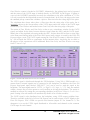
1.2 Specifications
Front Panel I/O
Signal Input (4x)
Logic Input/Output
4 analog inputs. Selectable input impedance: 50Ω and 2kΩ, ±2V pulsed,
±2V DC. Switch selectable input attenuation 1:8 and 1:1 for either
impedance setting.
General Purpose I/O connected to programmable logic:
1 MMCX coaxial connector and
1 high density 10-pin connector (single ended or differential)
Backplane I/O
Clock Input/Output
Triggers
Synchronization
Veto
Distributed 10 and 100 MHz clocks on PXIe backplane.
Wired-or bussed trigger on PXIe backplane for synchronous event
acquisition.
Wired-or SYNC signal distributed through PXIe backplane to
synchronize timers and run start/stop to 50ns.
Global logic level to suppress event triggering.
Data Interface
PCI Express
x4 connection to host PC.
Theoretical bandwidth 800 MB/s per slot
Actual bandwidth: ~450 MB/s
Digital Controls
Gain
Offset
Shaping
Trigger
Analog switched gain of 1.0 or 2.9
Digital gain adjustment of up to ±10% in 15ppm steps.
DC offset adjustment from –2.5V to +2.5V, in 65535 steps.
Digital trapezoidal filter. Rise time and flat top set independently in small
steps.
Digital trapezoidal trigger filter with adjustable threshold. Rise time and
flat top set independently.
Data Outputs
Spectrum
Statistics
Event data
1024-32768 bins per channel, 32 bit deep (4.2 billion counts/bin).
Additional memory for sum spectrum for clover detectors.
Real time, live time, filter and gate dead time, input and throughput
counts.
Pulse height (energy), timestamps, pulse shape analysis results,
waveform data and ancillary data like hit patterns.
4
PIXIE-500 Express User’s Manual V3.20
XIA 2014. All rights reserved.
2 Setting Up
2.1 Installation
2.1.1 Hardware Setup
The Pixie-500 Express modules can be operated in any standard 3U PXIe chassis. The total
system bandwidth will depend on the architecture of the chassis and controller – for maximum
bandwidth each slot should have an x4 connection (1 GB/s) and the controller should be capable
of 1 GB/s times the number of slots1.
A PXIe controller (embdded PC or bridge to desktop/laptop) must be placed in the system slot of
your chassis. Place the Pixie-500 Express modules into any peripheral PXIe or PXIe/PXI hybrid
slot with the chassis still powered down, then power up the chassis (Pixie-500 Express modules
are not hot swappable). If using a remote controller, be sure to boot the host computer after
powering up the chassis2.
2.1.2 Drivers and Software
System Requirements: The Pixie software is supported on Windows 7 and still compatible to
Windows XP and Vista. Restrictions apply to the 64 bit version of Windows 73. Please contact
XIA for details on operating Pixie-500 Express modules with Linux.
When the host computer is powered up the first time after installing the controller and Pixie-500
Express modules in the chassis, it will detect new hardware and try to find drivers for it. (A
Pixie-500 Express module will be detected as a new device every time it is installed in a new
slot.) While there is no required order of installation of the driver software, the following
sequence is recommended (users with embedded host computer skip to step 4):
1. If you have a remote controller, first install the driver software for the controller itself.
Otherwise, skip to step 4.
Unless directed otherwise by the manufacturer of the controller, this can be done with or
without the controller and Pixie-500 Express modules installed in the host computer
and/or chassis. If the modules are installed, ignore attempts by Windows to install drivers
until step 7.
NI controllers come with a multi-CD package called “Device Driver Reference CD”. For
simplicity it is recommended to install the software on these CDs in the default
configuration.
2. Unless already installed, power down the host computer, install the controller in both the
host computer and chassis, and power up the system again (chassis first).
1
Fast data rates will avoid or reduce dead times associated with data readout from module to host PC, but will only
matter at high count rates. Lower speed connections still work well for applications with lower data transfer
requirements.
2
In some systems, “scan for hardware changes” in the Windows device manager may detect and install a remote
chassis when the PC was booted first.
3
At the time of writing, these restrictions are: Support for 64bit Windows is still under development.
5
PIXIE-500 Express User’s Manual V3.20
XIA 2014. All rights reserved.
3. Windows will detect new hardware (the controller) and should find the drivers
automatically. Verify in Window’s device manager that the controller is properly
installed and has no “resource conflicts”.
4. Install Igor Pro
5. Install the Pixie-500 Express software provided by XIA (see section 2.2.3)
6. Unless already installed, power down the host computer and install the Pixie-500 Express
modules in the chassis. Check the input switch settings for the appropriate signal
termination: 50 Ω or 2 kΩ (see section 10.1 for details). Then power up the system again
(chassis first).
7. Windows will detect new hardware (the Pixie-500 Express modules) and should find the
drivers automatically. If not, direct it to the “drivers” directory in the Pixie-500 Express
software distribution installed in step 5. Verify in Window’s device manager that the
modules are properly installed as “Pixie500e” under Jungo devices and have no “resource
conflicts”.
2.1.3 Pixie User Interface
The Pixie Viewer, XIA’s graphical user interface to set up and run the Pixie-500 Express
modules (as well as other members of the Pixie family), is based on WaveMetrics’ IGOR Pro. To
run the Pixie Viewer, you have to have IGOR Version 5.0 or higher installed on your computer.
By default, IGOR Pro will be installed at C:\Program Files\WaveMetrics\IGOR Pro Folder.
The CD-ROM with the Pixie-500 Express software distribution contains the installation
program (for version XXX)
Pixie-500e_XXX_setup.exe
Follow the instructions shown on the screen to install the software to the default folder selected
by the installation program, or to a custom folder. This folder will contain the IGOR control
program (Pixie.pxp), online help files and 8 subfolders (Configuration, Doc, Drivers, DSP,
Firmware, MCA, PixieClib, and PulseShape). Make sure you keep this folder organization intact,
as the IGOR program and future updates rely on this. Feel free, however, to add folders and
subfolders at your convenience.
For the latest version of the Pixie Viewer software, go to support.xia.com and search for “Pixie
release”.
2.2 Getting Started
To start the Pixie Viewer, double-click on the file “Pixie.pxp” in the installation folder. After
IGOR loaded the Pixie Viewer, the START UP4 panel should be prominently displayed in the
middle of the desktop.
In the panel, first select the chassis type and number N of Pixie modules in the system. Then
specify the serial numbers of the modules – this allows addressing the modules from 0-N
independent of the physical slot.
4
In the following, SMALL CAPS are used for panel names; italic font is used for buttons and controls.
6
PIXIE-500 Express User’s Manual V3.20
XIA 2014. All rights reserved.
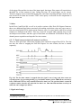
Figure 2.1: The Pixie Viewer START UP panel (above) and MAIN Panel
(right)
Click on the Start Up System button to initialize the modules. This
will download DSP code and FPGA configuration to the modules,
as well as the module parameters. If you see messages similar to
“Module 0 in slot 5 started up successfully!” in the IGOR history
window, the Pixie modules have been initialized successfully.
Otherwise, refer to the troubleshooting section for possible
solutions. If you want to try the software without a chassis or
modules attached, click on Offline Analysis.
After the system is initialized successfully, you will see the MAIN
control panel that serves as a shortcut to the most common actions
and from which all other panels are called. Its controls are organized in three groups: Setup, Run
Control, and Results.
In the Setup group, the Start System button opens the START UP panel in case you need to reboot
the modules. The Open Panels popup menu leads to four panels where parameters and
acquisition options are entered. They are described in more detail in section 3 and in the online
help. To get started, select Parameter Setup, which will open (or bring to front) the PARAMETER
SETUP panel shown in Figure 2.2. For most of the actions the Pixie Viewer interacts with one
Pixie module at a time. The number of that module is displayed at the top of the MAIN panel and
the top right of the PARAMETER SETUP panel. Proceed with the steps below to configure your
system.
Note: The More/Less button next to the Help button on the bottom of the PARAMETER SETUP panel
can be used to hide some controls. This may be helpful to first-time Pixie users who only want to
focus on the most essential settings.
7
PIXIE-500 Express User’s Manual V3.20
XIA 2014. All rights reserved.
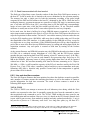
Figure 2.2: The PARAMETER SETUP Panel, Energy tab shown
For an initial setup, go through the following steps:
1. If not already visible, open the PARAMETER SETUP panel by selecting Parameter Setup from the
Open Panel popup menu in the MAIN panel.
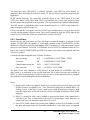
2. At the bottom of the PARAMETER SETUP panel, click on the Oscilloscope button. This opens
a graph that shows the untriggered signal input. (Fig.2.3)
In the OSCILLOSCOPE panel, click Refresh to update the display. The pulses should fall in
the display range (0-16K). If no pulses are visible or if they are cut off at the upper or
lower range of the display, click Adjust Offsets to automatically set the DC offset. If the
pulse amplitude is too large to fall in the display range, decrease the Gain. If the pulses
have falling leading edges, toggle the Invert checkbox.
Figure 2.3: OSCILLOSCOPE panel.
8
PIXIE-500 Express User’s Manual V3.20
XIA 2014. All rights reserved.
3. In the Energy tab of the PARAMETER SETUP panel, input an estimated preamplifier
exponential RC decay time for Tau, and then click on Auto Find Tau to determine the
actual Tau value for all channels of the current module. You can also enter a known good
Tau value directly in the Tau control field, or use the controls in the OSCILLOSCOPE to
manually fit Tau for a pulse.
4. Save the modified parameter settings to file. To do so, click on the Save button at the
bottom of the PARAMETER SETUP panel to open a save file dialog. Create a new file name to
avoid overwriting the default settings file.
5. Save the Igor experiment using File -> Save Experiment As from the top menu. This
saves the current state of the interface with all open panels and the settings for file paths
and slot numbers (the settings independent of module parameters).
6. Click on the Run Control tab, set Run Type to “0x301 MCA Mode”, Poll time to 1
second, and Run time to 30 seconds or so, then click on the Start Run button. A spinning
wheel will appear occasionally in the lower left corner of the screen as long as the system
is waiting for the run to finish. If you click the Update button in the MAIN panel, the count
rates displayed in the Results group are updated.
7. After the run is complete, select MCA Spectrum from the Open Panels popup menu in the
Results group of the MAIN panel. The MCA SPECTRUM graph shows the MCA histograms
for all four channels. You can deselect other channels while working on only one
channel. After defining a range in the spectrum with the cursors and setting the fit option
to fit peaks between cursors, you can apply a Gauss fit to the spectrum by selecting the
channels to be fit in the Fit popup menu. You can alternatively enter the fit limits using
the Min and Max fields in the table or by specifying a Range around the tallest peak or
the peak with the highest energy. To scale the spectrum in keV, enter the appropriate
ratio in the field keV/bin.
At this stage, you may not be able to get a spectrum with good energy resolutions. You may need
to adjust some settings such as energy filter rise time and flat top as described in section 3.5.
9
PIXIE-500 Express User’s Manual V3.20
XIA 2014. All rights reserved.
3 Navigating the Pixie Viewer
3.1 Overview
The Pixie Viewer consists of a number of graphs and control panels, linked together by the MAIN
control panel. The Viewer comes up in exactly the same state as it was when last saved to file
using File->Save Experiment. This preserves settings such as the file paths and the slot numbers
entered in the START UP panel. However, the Pixie module itself loses all programming when it is
switched off. When the Pixie module is switched on again, all programmable components need
code and configuration files to be downloaded to the module. Clicking on the Start Up System
button in the START UP panel performs this download. Below we describe the concepts and
principles of using the Pixie Viewer. Detailed information on the individual controls can be
found in the Online Help for each panel. The operating concepts are described in sections 4-7.
The controls in the MAIN control panel are organized in three groups: Setup, Run Control, and
Results. In the Setup and Results groups, popup menus lead to the panels and graphs indicated in
Figure 3.1.
Main
Setup
Boot
Run
Control
Start/Stop
Runtime
Run type
Results
Rates
Files/Path
Location of firmware,
settings, and output
files (3.2.4)
Chassis Setup
Trigger distribution and
coincidence between
modules (7.2.2, 7.6.2)
Oscilloscope
Analog gain and
offset (3.2.2)
FFT
Filter
Scan
Parameter Setup (3.2.1)
Trigger and threshold (3.2.1.1)
Gate and Veto (7.4)
Energy filter (3.2.1.2)
Coincidence between channels (7.6.1)
Waveform capture (3.2.1.3)
Run Control Options (3.2.1.7)
Copy
Extract
Record
options
MCA Spectrum
View energy histograms
(3.4.1)
File Series
View results from a
series of files (3.6)
List Mode Spectrum
Recreate MCA from list
mode data (3.4.2)
List Mode Traces
View waveforms and
event data (3.4.2)
Run Statistics
Live times and count
rates (3.4.3, 6.6)
History
Filter
Figure 3.1: Block diagram of the major panels in the Pixie Viewer. Numbers in brackets point to
the corresponding section in the user manual. All panels are described in detail in the online help.
10
PIXIE-500 Express User’s Manual V3.20
XIA 2014. All rights reserved.
3.2 Setup Group
In the setup group, there is a button to open the START UP panel, which is used to boot the
modules. The Open Panels popup menu leads to one of the following panels: PARAMETER SETUP,
OSCILLOSCOPE, CHASSIS SETUP, FILES/PATHS
3.2.1 PARAMETER SETUP Panel
The PARAMETER SETUP panel is divided into 7 tabs, summarized below. Settings for all four
channels of a module are shown in the same tab. At the upper right is a control to select the
module to address. At the bottom of the panel is a More button, which will make all advanced
panel controls visible as well.
The Pixie spectometer being a digital system, all parameter settings are stored in a settings file.
This file is separate from the Igor experiment file, to allow saving and restoring different settings
for different detectors and applications. Parameter files are saved and loaded with the
corresponding buttons at the bottom of the PARAMETER SETUP panel. After loading a settings file,
the settings are automatically downloaded to the module. At module initialization, the settings
are automatically read and applied to the Pixie module from the last saved settings file.
In addition there are buttons to copy settings between channels and modules, and to extract
settings from a settings file. Two large buttons at the lower left duplicate the buttons to call the
START UP panel and the OSCILLOSCOPE.
3.2.1.1 Trigger Tab
The Trigger tab contains controls to set the trigger filter parameters and the trigger threshold,
together with checkboxes to enable or disable trigger, to control trigger distribution (see section
7.2.1), and to set time stamping options for each channel. Except for the threshold, the trigger
settings have rarely to be changed from their default values.
The threshold value corresponds to ¼ of the pulse height in ADC steps, e.g. with a threshold of
20, triggers are issued for pulses above 80 ADC steps. This relation is true if the trigger filter
rise time is large compared to the pulse rise time and small compared to the pulse decay time. A
pulse shape not meeting these conditions has the effect of raising the effective threshold. For a
modeled behavior of the trigger, you can open displays from the OSCILLOSCOPE and the LIST MODE
TRACES panels that show trigger filter and threshold computed from acquired waveforms using
the current settings. The threshold value is scaled with the trigger filter rise time, therefore it is
not limited to integer numbers.
11
PIXIE-500 Express User’s Manual V3.20
XIA 2014. All rights reserved.
Figure 3.2: The Trigger tab of the PARAMETER SETUP panel.
3.2.1.2 Energy Tab
The Energy tab contains the settings for the energy filter and the subsequent computation. These
settings are most important for obtaining the best possible energy resolution with a Pixie system.
The energy filter rise time (or peaking time) essentially sets the tradeoff between throughput and
resolution: longer filter rise times generally improve the resolution (up to a certain optimum) but
reduce the throughput because more time is required to measure each pulse. The pulse decay
time Tau is used to compensate for the decay of a previous pulse in the computation of the pulse
height. You can enter a known good value, or click on Auto Find Tau to let the Pixie Viewer
determine the best value.
The advanced controls in this tab contain functions to modify the energy computation and to
acquire a series of measurements with varying filter settings and decay times to find the best
settings. For a detailed description of the filter operation, see section 6.
Figure 3.3: The Energy tab of the PARAMETER SETUP Panel.
12
PIXIE-500 Express User’s Manual V3.20
XIA 2014. All rights reserved.
3.2.1.3 Waveform Tab
The Waveform tab contains the controls to set the length and pre-trigger delay of the waveforms
to be acquired. Advanced options include parameters for online pulse shape analysis
3.2.1.4 Gate Tab
The Gate tab contains the controls to set the window for gating acquisition with external signals.
We define VETO as a signal distributed to all modules and channels, but each channel is
individually enabled to require or ignore this signal. VETO is active during the validation of a
pulse (after pileup inspection), an energy filter rise time plus flat top after the rising edge. With
suitable external logic, the decision to veto a pulse can be made from information obtained at the
rising edge of the pulse (e.g. multiplicity from several channels) and therefore this function is
also called Global First Level Trigger (GFLT).
For a detailed description of the VETO operation, see section 7.4.
3.2.1.5 Coincidence Tab
The Coincidence tab contains the controls to set the acceptable hit pattern, and the coincidence
window after validation during which channels can contribute to the hit pattern. There is a
checkbox for each possible hit pattern. For example, if the checkbox with pattern 0100 is
checked, events with a hit in channel 2 and no others are accepted. Selecting multiple
checkboxes accepts combinations of hit patterns, e.g. any event with exactly one channel hit.
For a detailed description of the coincidence operation, see section 7.2.1. Controls for
coincidences between modules are located in the CHASSIS SETUP Panel and described in section
7.2.2.
3.2.1.6 Advanced Tab
The Advanced tab contains the controls for modifying the pileup inspection, histogram
accumulation, baseline measurements, and ADC calibration. The ADC used on the Pixie-500
Express actually consists of two ADC cores on a single IC, which need to be calibrated for
matched gain, offset and phase. Normally, these calibration settings are read from the module's
non-volatile memory at boot time, but sometimes, for example at temperature changes, it may be
required to recalibrate the cores. An indication of mismatch are systematic offsets between odd
and even samples. These controls are repeated in the OSCILLOSCOPE panel.
3.2.1.7 Run Control Tab
The Run Control tab defines the settings for data acquisition. The “Run Type” popup menu
selects MCA or list mode runs, see section 4 for a detailed description. In addition, there are
controls
-
to set the run time (length of data acquisition as measured by Igor),
-
to set the polling time (period for checking if list mode data is available for readout
and/or run time is reached),
-
to specify the data file name (a base name plus 4-digit run number that can be made to
increment automatically), and
13
PIXIE-500 Express User’s Manual V3.20
XIA 2014. All rights reserved.
-
to specify the number of spills in list mode runs. (In list mode runs, data is accumulated
in on-board memory until full, at which time it is read out by the host PC. We call each
such readout a spill. The number of spills thus sets the amount of data to collect.)
The Start Run and Stop Run buttons from the MAIN control panel are duplicated here as well.
Advanced options include settings for synchronizing acquisition between modules, controls to
set a timeout for each spill, the number of events per spill, and the spill readout mode, and a
button to open a panel with advance record options.
Figure 3.4: The Run Control tab of the PARAMETER SETUP Panel.
3.2.2 OSCILLOSCOPE
As mentioned in section 2.3, the OSCILLOSCOPE (Figure 2.3) is used to view untriggered traces as
they appear at the ADC input and to set all parameters relating to the analog gain and offset.
There are controls titled
- dT [us], which sets the time between samples in the oscilloscope (there are always 8192
samples in the oscilloscope window),
- Offset [%], which sets the target DC-offset level for automatic adjustment,
- Gain (V/V), which sets the analog gain before digitization, and
- Offset (V), which directly sets the offset voltage.
The traces from different channels are not acquired synchronously but one after the other.
Therefore even if coincident signals are connected to the Pixie-500 Express inputs, the
OSCILLOSCOPE will show unrelated pulses for each channel.
There are also buttons and controls to
- open a display of the FFT of the input signal, which is useful to diagnose noise sources
- open a display of the waveforms of the trigger filter and energy filter computed from the
traces in the oscilloscope
- repeat the action of the Refresh button until a pulse is captured. This is useful for low
count rates.
- Fit the pulses in the OSCILLOSCOPE with an exponential decay function to determine the
decay time Tau, and to accept the fit value for the module settings.
14
PIXIE-500 Express User’s Manual V3.20
XIA 2014. All rights reserved.
-
View the current input count rate and the current fraction of time the signal is out of
range. These values are updated in the DSP every ~2-3ms independent of whether a run
is in progress or not. Their precision is in the order of 5-10%, or 50 cps.
Calibrate the ADC gain and offset matching of its two cores. Calibrations are reset at
every power cycle or reboot of the module, or by clicking the Reset button. The process
started with this button will measure the mismatch, then modify the gain and offset match
in an iterative process.
3.2.3 FILES/PATHS
The firmware files, DSP files and settings files are defined in the FILES/PATHS panel. Changes will
take effect at the next reboot, e.g. when clicking the Start Up System button in this panel or in the
START UP panel. There is also a button to set the files and paths to the default, relative to the
“home path” of the file Pixie.pxp.
Figure 3.5: The FILES/PATHS Panel.
15
PIXIE-500 Express User’s Manual V3.20
XIA 2014. All rights reserved.
3.2.4 CHASSIS SETUP
The CHASSIS SETUP panel is used to set parameters that affect the system as a whole. Examples are trigger
distribution between modules, coincidence settings between modules, and the operation of the Pixie-500
Express’s front panel input. See sections 7.2.2 and 7.6.2 for details.
3.3 Run Control Group
The Run Control group in the MAIN control panel has the most essential controls to start and stop
runs, and to define or monitor the run time and the number of spills. For more options, use the
Run Control tab of the PARAMETER SETUP panel.
3.4 Results Group
The Results group of the MAIN control panel displays the count rates of the current or most recent
run. Click Update to refresh these numbers.
The popup menu Open Panels leads to panels to view the output data from the data acquisition in
detail. These panels are the MCA SPECTRUM display, the LIST MODE TRACES display, the LIST MODE
SPECTRUM display, the RUN STATISTICS, and a panel to display results from a series of files.
3.4.1 MCA SPECTRUM
Figure 3.6: The MCA SPECTRUM display.
The MCA SPECTRUM display shows the spectra accumulated in on-board memory or from a .mca
file saved at the end of a run. Spectrum analysis is limited to fitting peaks with a Gaussian and
computing the peak resolution. There are several options to define the fit range, as described in
the online help. Spectra can be saved as text files for import into other applications.
16
PIXIE-500 Express User’s Manual V3.20
XIA 2014. All rights reserved.
3.4.2 LIST MODE TRACES and LIST MODE SPECTRUM
Figure 3.7: The LIST MODE TRACES display.
The LIST MODE TRACES display shows the data from the binary list mode files (.bin or .b## 5). If
waveforms were collected, they are shown in the graph section of the panel. Event and channel
header information – energy, time stamps, and hit patterns as described in section 4.1.2 – are
shown in the fields above the graph section. Key information bit of the hit pattern are decoded in
checkboxes below the hexadecimal value. After specifying a data file with the Find button, you
can select an event to view by entering its number in the Event Number field. In the binary file,
events are stored as single-channel records. To display data from coincident pulses in multiple
channels, check the box Show 4 pulses and enter a coincidence window in clock ticks. You will
have to increment the Event Number up to 4 times to get new data. The waveform from the
current event is displayed in bold. Arrow buttons allow changing of both module number and file
name at the same time.
The Ref popup menu allows one of the current 4 channels to be saved for comparison; check the
corresponding box in the table to add its waveform to the plot.
5
For multi-module runs, select the appropriate file b## for module ##.
17
PIXIE-500 Express User’s Manual V3.20
XIA 2014. All rights reserved.
The button Digital Filters opens a new plot that shows the response of the trigger filter and
energy filter computed from the list mode waveforms. This plot is more precise than the related
graph opened from the OSCILLOSCOPE since it uses the same full rate data, same as the filters
implemented in the module, not the reduced rate sampled at the OSCILLOSCOPE’S dT. However,
unless long list mode traces are acquired or energy filters are short, there may not be sufficient
data to compute the energy filter properly.
The LIST MODE SPECTRUM display is a plot similar to the MCA SPECTRUM, but it is computed from
the energies saved in the list mode data file. Since energies are stored there in full 16 bit
precision, binning can be made finer than in the MCA SPECTRUM, which is limited to 32K bins.
See the online help for a detailed description of the controls. Note that invalid events will have
energy=0, which causes a large spike in the first bin of the spectrum. Set Emin to a nonzero value
to hide this feature.
3.4.3 RUN STATISTICS
Figure 3.8: The RUN STATISTICS panel.
The RUN STATISTICS panel shows the live times and count rates measured by the Pixie-500
Express. The numbers can be updated by clicking the Update button and read from or save to
Files. For a detailed description of the definition of these values, see section 6.6.
3.4.4 FILE SERIES
See section 3.6 for a more detailed description
18
PIXIE-500 Express User’s Manual V3.20
XIA 2014. All rights reserved.
3.5 Optimizing Parameters
Optimization of the Pixie-500 Express’s run parameters for best resolution depends on the
individual systems and usually requires some degree of experimentation. The Pixie Viewer
includes several diagnostic tools and settings options to assist the user, as described below.
3.5.1 Noise
For a quick analysis of the electronic noise in the system, you can view a Fourier transform of
the incoming signal by selecting OSCILLOSCOPE FFT. The graph shows the FFT of the
untriggered input sigal of the OSCILLOSCOPE. By adjusting the dT control in the OSCILLOSCOPE and
clicking the Refresh button, you can investigate different frequency ranges. For best results,
remove any source from the detector and only regard traces without actual events. If you find
sharp lines in the 10 kHz to 1 MHz region you may need to find the cause for this and remove it.
If you click on the Apply Filter button, you can see the effect of the energy filter simulated on the
noise spectrum.
3.5.2 Energy Filter Parameters
The main parameter to optimize energy resolution is the energy filter rise time. Generally, longer
rise times result in better resolution, but reduce the throughput. Optimization should begin with
scanning the rise time through the available range. Try 2µs, 4µs, 8µs, 11.2µs, take a run of 60s or
so for each and note changes in energy resolution. Then fine tune the rise time.
The flat top usually needs only small adjustments. For a typical coaxial Ge-detector we suggest
to use a flat top of 1.2µs. For a small detector (20% efficiency) a flat top of 0.8µs is a good
choice. For larger detectors flat tops of 1.2µs and 1.6µs will be more appropriate. In general the
flat top needs to be wide enough to accommodate the longest typical signal rise time from the
detector. It then needs to be wider by one filter clock cycle than that minimum, but at least 3
filter clock cycles. Note that a filter clock cycle ranges from 0.026 to 0.853µs, depending on the
filter range, so that it is not possible to have a very short flat top together with a very long filter
rise time.
The Pixie Viewer provides a tool to create a file series where the energy filter parameters are
modified for each file in the series. See section 3.6 for more details.
3.5.3 Threshold and Trigger Filter Parameters
In general, the trigger threshold should be set as low as possible for best resolution. If too low,
the input count rate will go up dramatically and “noise peaks” will appear at the low energy end
of the spectrum. If the threshold is too high, especially at high count rates, low energy events
below the threshold can pass the pile-up inspector and pile up with larger events. This increases
the measured energy and thus leads to exponential tails on the (ideally Gaussian) peaks in the
spectrum. Ideally, the threshold should be set such that the noise peaks just disappear.
The settings of the trigger filter have only minor effect on the resolution. However, changing the
trigger conditions might have some effect on certain undesirable peak shapes. A longer trigger
rise time allows the threshold to be lowered more, since the noise is averaged over longer
periods. This can help to remove tails on the peaks. A long trigger flat top will help to trigger
better on slow rising pulses and thus result in a sharper cut off at the threshold in the spectrum.
19
PIXIE-500 Express User’s Manual V3.20
XIA 2014. All rights reserved.
3.5.4 Decay Time
The preamplifier decay time τ is used to correct the energy of a pulse sitting on the falling slope
of a previous pulse. The calculations assume a simple exponential decay with one decay
constant. A precise value of τ is especially important at high count rates where pulses overlap
more frequently. If τ is off the optimum, peaks in the spectrum will broaden, and if τ is very
wrong, the spectrum will be significantly blurred.
The first and usually sufficiently precise estimate of τ can be obtained from the Auto Find
routine in the Energy tab of the PARAMETER SETUP panel. Measure the decay time several times
and settle on the average value.
Fine tuning of τ can be achieved by exploring small variations around the fit value (±2-3%). This
is best done at high count rates, as the effect on the resolution is more pronounced. The value of
τ found through this way is also valid for low count rates. Manually enter τ , take a short run, and
note the value of τ that gives the best resolution.
Pixie users can also use the fit routines in the OSCILLOSCOPE to manually find the decay time
through exponentially fitting the untriggered input signals. Another tool is to create a file series
where τ is modified for each file in the series. See section 3.6 for more details.
3.5.5 Baselines and ADC calibration
Between detector pulses, the Pixie module continuously measures baselines, which is ultimately
used to correct for the DC offset. Multiple baseline measurements can be averaged to reduce
noise, and a threshold can be set to exclude the occasional bad measurement from the average.
The controls to set these parameters are located in the Advanced tab of the PARAMETER SETUP
panel. The optimum values depend on the detector used; but usually the defaults are good
estimates and resolutions only improve slightly with manual fine tuning.
The 500 MHz ADC used on the Pixie-500 Express is actually a combination of two 250 MHz
ADC cores on a single IC. For best performance, the two cores have to be calibrated to match in
gain, offset and phase. Default ADC calibration values are stored on an on-board EEPROM and
are applied to the ADCs at boot time. It may happen that the default values are not suitable, e.g.
due to significant temperature drifts. This would manifest itself as a distinct offset between even
and odd samples in the waveforms. In such a case, the ADCs can be recalibrated with a routine
called from a button in the Advanced tab of the PARAMETER SETUP panel.
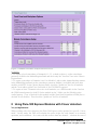
3.6 File Series
3.6.1 File Series to break up long data acquisition runs
When taking long data acquisitions, it may be beneficial to break up the run into smaller sub
runs. This helps to save data in case of power failure or system crashes, since only the most
recent sub run is lost. Also list mode files tend to get large and unwieldy for analysis in longer
runs, and 32bit operating systems may impose a 4 GB limit.
The Pixie Viewer thus has a method to create a series of files at specified intervals. In the DATA
RECORD OPTIONS panel, opened with the Record button in the Run Control tab of the PARAMETER
SETUP panel, there is a checkbox named New files every, followed by a control field to enter a
20
PIXIE-500 Express User’s Manual V3.20
XIA 2014. All rights reserved.
spill (or time) interval N. If checked and a run is started, every N spills (or, in MCA runs, every
N seconds) the data file is closed, spectra, settings and statistics are saved, and then a new run is
started. This is equivalent to manually clicking first the Stop Run button and then the Start Run
button. It is recommended to enable the automatic increment and auto-store options as shown in
Figure 3.9 as well.
Figure 3.9: The DATA RECORD OPTIONS panel with checkboxes set to acquire a series of files.
3.6.2 File Series to scan filter parameters
With some modifications, the mechanism to create file series described in section 3.6.1 can also
be used to scan through a range of energy filter or decay time settings. This is equivalent to
starting an MCA run with initial settings, stopping the run, incrementing the energy filter rise
time, restarting the run, and so on. The file series will thus contain spectra for a whole range of
settings, which can be analyzed manually or with the routine described in section 3.6.3.
21
PIXIE-500 Express User’s Manual V3.20
XIA 2014. All rights reserved.
Figure 3.10: The FILE SERIES SCAN panel to acquire a series of files in which energy filter parameters
and Tau are varied within user defined limits.
To set up such a parameter scan, open the FILE SERIES SCAN panel (PARAMETER SETUP -> Energy tab
-> Scan Settings) shown in Figure 3.10. A control field named Filter Range is repeated from the
Energy tab. In three groups of controls, you can set the start, end, and step size for varying the
energy filter rise time, the energy filter flat top, and Tau. If the step size is zero, that parameter
will not be varied.
Two buttons assist in setting up the initial conditions: Set Parameters to Start sets the current
values of the energy filter and Tau to the start value defined in the File Series Scan panel. If you
omit to click this button, the file series will begin with the current value; this is useful to resume
a file series. Set Scan Run Conditions will set the checkboxes in the DATA RECORD OPTIONS panel to
the values required for the scan, and set the run time to the total time required (interval N in the DATA
RECORD OPTIONS panel times the number of settings).
At the bottom of the panel, the button Start Scan starts the file series. This is a different button
from the standard Start Run button, because it is starting a run which is modifying parameters.
All the updates during a run work the same as in a standard run, though; and the run can be
stopped with the standard Stop Run button. When the run is complete, click on the File Series
button to open the panel described in section 3.6.3
22
PIXIE-500 Express User’s Manual V3.20
XIA 2014. All rights reserved.
3.6.3 File Series Analysis
Figure 3.11: The FILE SERIES RESULTS plot to analyze a series of files from a parameter scan.
To analyze a series of .mca files, you can use the FILE SERIES RESULTS panel. Enter the base name
and the start and end run numbers of the series, then click Parse Files. Start and end are
inclusive, i.e. for start = 1 and end =13, the parsing covers files base0001-base0013. An .ifm file
is required to read the values for Tau and the filter settings. The parsing routine reads the spectra
and fits peaks with the options set in the MCA SPECTRUM. Thus make sure the fit range is set
appropriately. In the plot, the peak position and resolution is plotted as a function of run number,
together with the filter settings and tau for each channel selected.
23
PIXIE-500 Express User’s Manual V3.20
XIA 2014. All rights reserved.
4 Data Runs and Data Structures
4.1 Run Types
There are two major run types: MCA runs and List mode runs. MCA runs only collect spectra
and run statistics, List mode runs acquire data on an event-by event basis, but also collect spectra
and run statistics. List mode runs come in several variants (see below), storing different amounts
of data per event.
The output data are stored in three different memory blocks. The MCA block resides in a
dedicated spectrum memory. List mode data is stored in 256 MB of SDRAM organized as a
FIFO. Run statistics are kept in local memory by the on-board FPGA.
4.1.1 MCA Runs
If only energy spectra are of interest, an MCA run should be used. For each event, this type of
run collects the data necessary to calculate pulse heights (energies) only. The energy values are
used to increment the MCA spectrum. The run continues until the host computer stops data
acquisition, either by reaching the run time set in the Pixie Viewer, or by a manual stop from the
user (the module does not stop by itself).
There is no data transferred between the Pixie module and the host PC, except for the occasional
manual update of MCA spectra and run statistics. By design, the MCA memory does not “fill
up” – each event simply increments a bin in the spectrum6.
4.1.2 List Mode Runs
If, on the other hand, data should be collected on an event-by-event basis, including energies,
time stamps, pulse shape analysis values, and wave forms, a list mode run should be used. In list
mode, pulse heights are still histogrammed into MCA spectra, e.g. for monitoring purposes. The
list mode data is continuously transferred from the Pixie module to the host PC.
List mode runs halt data acquisition either when a preset time is reached, or when a preset
number of “spills” have been collected, as determined by the Pixie Viewer. A spill here means
2 MB of data read from the SDRAM FIFO. Unlike the Pixie-4 or Pixie-500, the Pixie-500
Express never stops the acquisition for data readout. List mode data is buffered in the SDRAM
FIFO, and read by the host PC on one end while being written by the firmware on the other end.
Given the data bandwidth of the PXIe interface, it is rather unlikely for the SDRAM to fill up,
except for situations with very high rates and very long waveforms. (If the SDRAM actually
does fill up, data acquisition is paused but as soon as the host frees up SDRAM memory by
reading and storing data to disk, the acquisition continues. The red light on the module's front
panel indicates such a condition.)
When the Pixie Viewer ends the data acquisition, there may be data in the SDRAM that has not
yet been stored to file. The readout thus continues for a short while after the DSP stops collecting
6
Rollovers from 232 to 0 may happen for extremely long runs and/or extremely high count rates
24
PIXIE-500 Express User’s Manual V3.20
XIA 2014. All rights reserved.
new data, adding one or more spills to the file. The preset number of spills is therefore to be
understood as a minimum request.
4.1.2.1 Pulse Shape Analysis
Pulse shape analysis comes in several varieties, executing algorithms by XIA (enabled by
selecting options in the standard firmware/software) or algorithms programmed by users as plugin code for the DSP. In the current firmware/software, the following algorithms are available
from XIA:
– Accumulation of 2 sums (baseline subtracted) near the rising edge of the pulse.
– Capture of amplitude (maximum minus baseline) near the rising edge of the pulse.
– Computation of the ratio of the 2 sums
Please contact XIA for details.
4.1.2.2 Compressed Data Formats
The output data of list mode runs can be reduced by using one of the compressed formats
described below. The key differences are that as less data is recorded for each event, there is
room for more events in the SDRAM FIFO, less time is spent per event to read out data to the
host computer, and data files are smaller. These compressed data formats are currently under
development.
Table 4.1: Summary of run types and data formats.
Run Type
Output data
DSP Variables
MCA Mode
List Mode
(standard)
Spectra in MCA memory
Energies, time stamps, PSA values, and wave
forms in List mode memory.
Spectra in MCA memory
RUNTASK = 0x301
RUNTASK = 0x400
(CHANHEADLEN = 32)
4.2 Output Data Structures
4.2.1 MCA Histogram Data
The MCA memory currently uses 32K words (32-bit deep) per channel, i.e. total 128K words.
The memory can be read out via the PCIe data bus at any time, though not at the full burst rate. If
spectra of less than 32K length are requested, only part of the 32K will be filled with data.
The total MCA memory size on the Pixie-500 Express is 512K words. It can be reorganized for
special applications (e.g., 2D spectra or channel sum spectra).
25
PIXIE-500 Express User’s Manual V3.20
XIA 2014. All rights reserved.
If enabled, the histogram data is automatically read and saved to file at the end of the run. The
file has the extension .mca.
4.2.2 List Mode Data
The list mode data in the SDRAM FIFO consists of a series of single channel data records. For
each module, the host readout process creates an individual file for these records. The extension
of these files is .b## (## = 2 digit module number). The records can be written by the DSP in a
number of formats. User code should access the data in the file header to navigate through the
data. The file should only be read when the run has ended.
The data organization of one file is as follows. The file always starts with a file header of length
BUFHEADLEN. Currently, BUFHEADLEN is 32, and the 32 words (16 bit) are:
Table 4.2: File header data format, total 32 words (16bit)
Word #
0
1
2
3
4
5
6
Variable
BlkSize
ModNum
RunFormat
ChanHeadLen
CoincPat
CoincWin
MaxCombTraceLen
7--32
unused
Description
Block size (16-bit words)
Module number
Format descriptor = RunTask
Channel Header Length
Coincidence pattern
Coincidence window
Maximum length of traces from all 4 channels (in
blocks)
reserved
Following the file header, the single channel event records are stored in sequential order. Each
event starts out with an channel header of length ChanHeadLen. Currently, ChanHeadLen=32,
and the 32 words (16 bit) are:
Table 4.3: Channel header data format.
Word
#
0
1
2
3
4
5
6
7
8
9
10
11
12--15
16--32
Variable
Description
EvtPattern
EvtInfo
NumTraceBlks
NumTraceBlksPrev
TrigTimeLO
TrigTimeMI
TrigTimeHI
TrigTimeX
Energy
ChanNo
User PSA Value
XIA PSA Value
Extended PSA Values
reserved
Hit pattern.
Event status flags.
Number of blocks of Trace data to follow the header
Number of blocks of Trace data in previous record (for parsing back)
Trigger time, low word
Trigger time, middle word
Trigger time, high word
Trigger time, extra 8 bits
Pulse Height
Channel number
Result of User specific pulse shape analysis
Result of standard XIA pulse shape analysis
The hit pattern is a bit mask, which tells which channels were captured within the specified
coincidence window plus some additional status information, as listed in table 4.4. The channel
26
PIXIE-500 Express User’s Manual V3.20
XIA 2014. All rights reserved.
header may be followed by waveform data. An offline analysis program can recognize this by
reading the number of waveform blocks from the NumTraceBlks word. The block size is defined
in the file header.
Table 4.4: Event Pattern and Event Info bit description.
Bit #
Description
EvtPattern
0..3
If set, indicates that data for channel 0..3 have been recorded
4..7
4: Logic level of FRONT panel input
5: Result of LOCAL acceptance test
6: Logic level of backplane STATUS line,
7: Logic level of backplane TOKEN line (= result of global coincidence test), see section 7
8..11
If set, indicates that channel 0..3 has been hit in this event
(i.e. if zero, energy reported is invalid or only an estimate)
12..15
reserved
EvtInfo
0
Coincidence test result
1
Logic level of backplane VETO line
2
If set, indicates event is piled up
3
If set, indicates waveform FIFO full
4
If set, indicates this channel was hit (else the event was recorded based on distributed trigger)
5..15_4
reserved
4.2.3 Reconstruction of List Mode Time Stamps
In the Pixie-500 Express, there is a 56-bit time counter that is reset to zero at boot time or at a
run start with the “synchronize clocks” option selected. It is incremented at a rate of 125 MHz by
4 ticks, so that the unit of the LSB is 2ns. Hence, the 56-bit word can span a time interval of over
800 days before rolling over.
The full 56 bit time stamp is recorded in every channel header. Compressed data formats may
store less bits in the future.
27
PIXIE-500 Express User’s Manual V3.20
XIA 2014. All rights reserved.
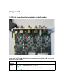
5 Hardware Description
The Pixie-500 Express is a 4-channel unit designed for gamma-ray spectroscopy and waveform
capturing. It incorporates four functional building blocks, which we describe below. This section
concentrates on the functionality aspect. Technical specification can be found in section 1.2.
Figure 5.1 shows the functional block diagram of the Pixie-500 Express.
Figure 5.1: Functional block diagram of the Pixie-500 Express front-end data acquisition and signal
processing card.
5.1 Analog Signal Conditioning
Each analog input has its own signal conditioning unit. The task of this circuitry is to adapt the
incoming signals, which are DC coupled, to the input voltage range of the ADC, which spans
2 V. Input signals are adjusted for offsets, and there is a computer-controlled gain stage of
switched relays. A fine tuning of the gain is achieved by multiplying the calculated energy values
with digital gain factors in the digital signal processor (DSP). Four options of termination and
attenuation are selected by manual switches at the front end of the module.
The ADC is not a peak sensing ADC, but acts as a waveform digitizer. In order to avoid aliasing,
we remove the high frequency components from the incoming signal prior to feeding it into the
ADC. The anti-aliasing filter, an active Sallen-Key filter, cuts off sharply at the Nyquist
frequency, namely half the ADC sampling frequency.
28
PIXIE-500 Express User’s Manual V3.20
XIA 2014. All rights reserved.
Though the Pixie-500 Express can work with many different signal forms, best performance is to
be expected when sending the output from a charge integrating preamplifier directly to the
Pixie-500 Express without any further shaping.
5.2 Pulse Processing
Real time pulse processing is implemented in a field programmable gate array (FPGA) which
also incorporates FIFO memory for each channel. The data stream from the ADCs is sent to
these units at the full ADC sampling rate. While modern FPGAs can capture high speed data
streams, internal processing is limited by the complexity of the logic. Therefore, the FPGA on
the Pixie-500 Express internally “de-serializes” each channel's 14-bit, 500 MHz data stream into
a 56-bit, 125 MHz data stream for processing. Using a pipelined architecture, the signals are
processed at this high rate, without the help of the on-board DSP.
The processing applies digital filtering to perform essentially the same action as a shaping
amplifier. The important difference is in the type of filter used. In a digital application it is easy
to implement finite impulse response filters, and we use a trapezoidal filter. The flat top will
typically cover the rise time of the incoming signal and makes the pulse height measurement less
sensitive to variations of the signal shape.
The first two processing elements in the FPGA are thus a fast filter for triggering and a slow
filter for pulse height (energy) measurements. For a detailed description, see section 6. These
filters run continuously. Triggers are issued at each detected rising edge, latch time stamps, and
are used for the other processes. The energy filter sums are latched the appropriate time after
each trigger.
A third processing element is a pileup inspector. This logic ensures that if a second pulse is
detected too soon after the first, so that it would corrupt the first pulse height measurement, both
pulses are flagged as piled up. The pileup inspector is, however, not very effective in detecting
pulse pileup on the rising edge of the first pulse, i.e. in general pulses must be separated by their
rise time to be effectively recognized as different pulses. Therefore, for high count rate
applications, the pulse rise times should be as short as possible, to minimize the occurrence of
pileup peaks in the resulting spectra.
The fourth processing component is the FIFO memory, which is organized in two blocks. A
smaller delay FIFO (2K samples) buffers ADC data to position captured waveforms
appropriately for the user defined pre-trigger delay. A larger storage FIFO (8K samples)
captures waveforms of the user defined trace length.
Up to 16 events and 8K samples of waveforms are buffered in the FPGA. For each event, a
complete set of time stamps, energy filter sums, pileup inspection flags, coincidence information
and waveforms are stored. Waveforms from closely following events may overlap, i.e. the same
ADC data is stored once but read twice for subsequent events. User defined acceptance settings
specify if an event is considered valid (e.g. only accept events without pileup).
The last processing element are a number of counters that keep run statistics such as live time,
filter dead time, number of triggers, and so on.
29
PIXIE-500 Express User’s Manual V3.20
XIA 2014. All rights reserved.
5.3 Digital Signal Processor (DSP) and Event Building
The pulse processing described above runs independently in every channel of the Pixie module.
On a module-wide level, additional logic is implemented to distribute triggers and apply a
coincidence test. See section 7 for details. The result of the coincidence test is fed back to every
processing channel.
The DSP manages the flow of channel data into the SDRAM buffer. Whenever a channel has an
event in its buffer, the DSP will read the raw data from the FPGA and based on the event status
flags determine if the event is to be recorded. (At this point, there is also the option of executing
customized user DSP code to modify results and the acceptance decision.) If the event is
acceptable, the DSP computes the pulse height in a few floating point operations, and includes it
in the event header data sent to the SDRAM. The captured waveform data is normally not
touched by the DSP; the DSP only enables a direct FPGA-internal transfer from the channel
processing block to the SDRAM interface block, at a rate of 1GByte/s.
The DSP also controls the overall operation of the Pixie-500 Express. The host computer
communicates with the DSP via the PCIe interface. Reading and writing data to DSP memory
does only temporarily pause its operation, and can occur even while a measurement is underway.
The host sets variables in the DSP memory and if necessary calls DSP functions to apply them to
the FPGA. Through this mechanism all gain and offset DACs are set and the filter settings are
applied to the FPGA. The FPGA then processes the data without support from the DSP, once it
has received the filter settings.
In this scheme, the greatest processing power is located in the FPGA, processing the incoming
waveforms from the ADCs in real time and producing, for each valid a event, a small set of
distilled data from which pulse heights and arrival times can be reconstructed. The computational
load for the DSP is much reduced, as it has to react only on an event-by-event basis and has to
work with only a small set of numbers for each event.
5.4 PCI Express Interface
The PCI Express (PCIe) interface through which the host communicates with the Pixie-500
Express is implemented in a PCIe endpoint IC which is linked to the FPGA by a local bus. At
this time, the interface does not issue interrupt requests to the host computer (but it may do so in
the future). Instead, for example to determine the run status, the host has to poll a Control and
Status Register (CSR) in the FPGA.
The FPGA links the PCIe IC with the DSP and the on-board memory. The host can read out the
memory without interrupting the operation of the DSP. This allows updates of the MCA
spectrum or list mode data while a run is in progress.
A dedicated I/O FPGA distributes triggers and coincidence signals to other modules using the
PXI backplane connections and the front panel connectors.
30
PIXIE-500 Express User’s Manual V3.20
XIA 2014. All rights reserved.
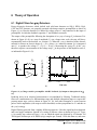
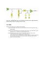
6 Theory of Operation
6.1 Digital Filters for γ-ray Detectors
Energy dispersive detectors, which include such solid state detectors as Si(Li), HPGe, HgI2,
CdTe and CZT detectors, are generally operated with charge sensitive preamplifiers as shown in
Figure 6.1 (a). Here the detector D is biased by voltage source V and connected to the input of
preamplifier A which has feedback capacitor Cf and feedback resistor Rf.
The output of the preamplifier following the absorption of an γ-ray of energy Ex in detector D is
shown in Figure 6.1 (b) as a step of amplitude Vx (on a longer time scale, the step will decay
exponentially back to the baseline, see section 6.3). When the γ-ray is absorbed in the detector
material it releases an electric charge Qx = Ex/ε, where ε is a material constant. Qx is integrated
onto Cf, to produce the voltage Vx = Qx/Cf = Ex/(εCf). Measuring the energy Ex of the γ-ray
therefore requires a measurement of the voltage step Vx in the presence of the amplifier noise σ,
as indicated in Figure 6.1 (b).
Rf
V
Cf
D
A
Preamp Output (mV)
4
2
σ
-2
-4
0.00
a)
Vx
0
0.02
0.04
0.06
Time (ms)
b)
Figure 6.1: (a) Charge sensitive preamplifier with RC feedback; (b) Output on absorption of an γray.
Reducing noise in an electrical measurement is accomplished by filtering. Traditional analog
filters use combinations of a differentiation stage and multiple integration stages to convert the
preamp output steps, such as shown in Figure 6.1 (b), into either triangular or semi-Gaussian
pulses whose amplitudes (with respect to their baselines) are then proportional to Vx and thus to
the γ-ray’s energy.
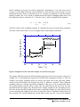
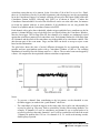
Digital filtering proceeds from a slightly different perspective. Here the signal has been digitized
and is no longer continuous. Instead it is a string of discrete values as shown in Figure 6.2. Figure
6.2 is actually just a subset of Figure 6.1 (b), in which the signal was digitized by a Tektronix 544
TDS digital oscilloscope at 10 MSPS (mega samples per second). Given this data set, and some
31
PIXIE-500 Express User’s Manual V3.20
XIA 2014. All rights reserved.
kind of arithmetic processor, the obvious approach to determining Vx is to take some sort of
average over the points before the step and subtract it from the value of the average over the
points after the step. That is, as shown in Figure 6.2, averages are computed over the two regions
marked “Length” (the “Gap” region is omitted because the signal is changing rapidly here), and
their difference taken as a measure of Vx. Thus the value Vx may be found from the equation:
V x ,k = −
∑
WiVi +
i ( before )
∑
WiVi
(6.1)
i ( after )
where the values of the weighting constants Wi determine the type of average being computed.
The sums of the values of the two sets of weights must be individually normalized.
Preamp Output (mV)
4
2
Length
G ap
0
Length
-2
-4
20
22
24
26
28
30
Time ( µ s)
Figure 6.2: Digitized version of the data of Figure 6.1 (b) in the step region.
The primary differences between different digital signal processors lie in two areas: what set of
weights { Wi } is used and how the regions are selected for the computation of Eqn. 6.1. Thus, for
example, when larger weighting values are used for the region close to the step while smaller
values are used for the data away from the step, Eqn. 6.1 produces “cusp-like” filters. When the
weighting values are constant, one obtains triangular (if the gap is zero) or trapezoidal filters.
The concept behind cusp-like filters is that, since the points nearest the step carry the most
information about its height, they should be most strongly weighted in the averaging process.
How one chooses the filter lengths results in time variant (the lengths vary from pulse to pulse)
or time invariant (the lengths are the same for all pulses) filters. Traditional analog filters are
time invariant. The concept behind time variant filters is that, since the γ-rays arrive randomly
32
PIXIE-500 Express User’s Manual V3.20
XIA 2014. All rights reserved.
and the lengths between them vary accordingly, one can make maximum use of the available
information by setting the length to the interpulse spacing.
In principle, the very best filtering is accomplished by using cusp-like weights and time variant
filter length selection. There are serious costs associated with this approach however, both in
terms of computational power required to evaluate the sums in real time and in the complexity of
the electronics required to generate (usually from stored coefficients) normalized { Wi } sets on a
pulse by pulse basis.
The Pixie-500 Express takes a different approach because it was optimized for high speed
operation. It implements a fixed length filter with all Wi values equal to unity and in fact
computes this sum afresh for each new signal value k. Thus the equation implemented is:
LV x ,k = −
k − L− G
∑
Vi +
k
∑
Vi
(6.2)
i= k − 2 L− G+ 1 i= k − L+ 1
where the filter length is L and the gap is G . The factor L multiplying Vx ,k arises because the
sum of the weights here is not normalized. Accommodating this factor is trivial.
While this relationship is very simple, it is still very effective. In the first place, this is the digital
equivalent of triangular (or trapezoidal if G ≠ 0) filtering which is the analog industry’s standard
for high rate processing. In the second place, one can show theoretically that if the noise in the
signal is white (i.e. Gaussian distributed) above and below the step, which is typically the case
for the short shaping times used for high signal rate processing, then the average in Eqn. 6.2
actually gives the best estimate of Vx in the least squares sense. This, of course, is why triangular
filtering has been preferred at high rates. Triangular filtering with time variant filter lengths can,
in principle, achieve both somewhat superior resolution and higher throughputs but comes at the
cost of a significantly more complex circuit and a rate dependent resolution, which is
unacceptable for many types of precise analysis. In practice, XIA’s design has been found to
duplicate the energy resolution of the best analog shapers while approximately doubling their
throughput, providing experimental confirmation of the validity of the approach.
6.2 Trapezoidal Filtering in a Pixie Module
From this point onward, we will only consider trapezoidal filtering as it is implemented in a
Pixie module according to Eqn. 6.2. The result of applying such a filter with Length L=1µs and
Gap G=0.4µs to a γ-ray event is shown in Figure 6.3. The filter output is clearly trapezoidal in
shape and has a rise time equal to L, a flattop equal to G, and a symmetrical fall time equal to L.
The basewidth, which is a first-order measure of the filter’s noise reduction properties, is thus
2L+G.
This raises several important points in comparing the noise performance of the Pixie module to
analog filtering amplifiers. First, semi-Gaussian filters are usually specified by a shaping time.
Their rise time is typically twice this and their pulses are not symmetric so that the basewidth is
about 5.6 times the shaping time or 2.8 times their rise time. Thus a semi-Gaussian filter
typically has a slightly better energy resolution than a triangular filter of the same rise time
because it has a longer filtering time. This is typically accommodated in amplifiers offering both
33
PIXIE-500 Express User’s Manual V3.20
XIA 2014. All rights reserved.
triangular and semi-Gaussian filtering by stretching the triangular rise time a bit, so that the true
triangular rise time is typically 1.2 times the selected semi-Gaussian rise time. This also leads to
an apparent advantage for the analog system when its energy resolution is compared to a digital
system with the same nominal rise time.
One important characteristic of a digitally shaped trapezoidal pulse is its extremely sharp
termination on completion of the basewidth 2L+G. This may be compared to analog filtered
pulses whose tails may persist up to 40% of the rise time, a phenomenon due to the finite
bandwidth of the analog filter. As we shall see below, this sharp termination gives the digital
filter a definite rate advantage in pileup free throughput.
ADC output
Filter Output
3
ADC units
33x10
32
31
G
L
2L+G
30
9.5
10.0
10.5
11.0
Time
11.5
12.0
12.5µs
Figure 6.3: Trapezoidal filtering of a preamplifier step with L=1µs and G=0.4µs.
6.3 Baselines and Preamplifier Decay Times
Figure 6.4 shows an event over a longer time interval and how the filter treats the preamplifier
noise in regions when no γ-ray pulses are present. As may be seen the effect of the filter is both
to reduce the amplitude of the fluctuations and reduce their high frequency content. This region
is called the baseline because it establishes the reference level from which the γ-ray peak
amplitude Vx is to be measured. The fluctuations in the baseline have a standard deviation σe
which is referred to as the electronic noise of the system, a number which depends on the rise
time of the filter used. Riding on top of this noise, the γ-ray peaks contribute an additional noise
term, the Fano noise, which arises from statistical fluctuations in the amount of charge Qx
produced when the γ-ray is absorbed in the detector. This Fano noise σf adds in quadrature with
the electronic noise, so that the total noise σt in measuring Vx is found from
σt = sqrt( σf2 + σe2)
34
(3)
PIXIE-500 Express User’s Manual V3.20
XIA 2014. All rights reserved.
The Fano noise is only a property of the detector material. The electronic noise, on the other
hand, may have contributions from both the preamplifier and the amplifier. When the
preamplifier and amplifier are both well designed and well matched, however, the amplifier’s
noise contribution should be essentially negligible. Achieving this in the mixed analog-digital
environment of a digital pulse processor is a non-trivial task, however.
3
33x10
σt
32
ADC units
ADC Output
Filter Output
31
30
Vx
σe
29
28
75
80
85
90
95µs
Time
Figure 6.4: A γ-ray event displayed over a longer time period to show baseline noise and the effect
of preamplifier decay time.
With a RC-type preamplifier, the slope of the preamplifier is rarely zero. Every step decays
exponentially back to the DC level of the preamplifier. During such a decay, the baselines are
obviously not zero. This can be seen in Figure 6.4, where the filter output during the exponential
decay after the pulse is below the initial level. Note also that the flat top region is sloped
downwards.
Using the decay constant τ, the baselines can be mapped back to the DC level. This allows
precise determination of γ-ray energies, even if the pulse sits on the falling slope of a previous
pulse. The value of τ, being a characteristic of the preamplifier, has to be determined by the user
and host software and downloaded to the module.
6.4 Thresholds and Pile-up Inspection
As noted above, we wish to capture a value of Vx for each γ-ray detected and use these values to
construct a spectrum. This process is also significantly different between digital and analog
systems. In the analog system the peak value must be “captured” into an analog storage device,
usually a capacitor, and “held” until it is digitized. Then the digital value is used to update a
memory location to build the desired spectrum. During this analog to digital conversion process
the system is dead to other events, which can severely reduce system throughput. Even single
channel analyzer systems introduce significant deadtime at this stage since they must wait some
35
PIXIE-500 Express User’s Manual V3.20
XIA 2014. All rights reserved.
period (typically a few microseconds) to determine whether or not the window condition is
satisfied.
Digital systems are much more efficient in this regard, since the values output by the filter are
already digital values. All that is required is to take the filter sums, reconstruct the energy Vx,
and add it to the spectrum. In the Pixie-500 Express, the filter sums are continuously updated in
the FPGA (see section 5.2), and only have to be read out by the DSP when an event occurs.
Reconstructing the energy and incrementing the spectrum is done by the DSP, so that the FPGA
is ready to take new data immediately after the readout. This usually takes much less than one
filter rise time, so that no system deadtime is produced by a “capture and store” operation. This
is a significant source of the enhanced throughput found in digital systems.
3
32x10
ADC Output
Fast Filter Output
Slow Filter Output
31
ADC units
30
29
28
Sampling Time
Arrival Time
27
Threshold
26
44
45
46
47
48µs
Time
Figure 6.5: Peak detection and sampling in a Pixie module.
The peak detection and sampling in a Pixie module is handled as indicated in Figure 6.5. Two
trapezoidal filters are implemented, a fast filter and a slow filter. The fast filter is used to detect
the arrival of γ-rays, the slow filter is used for the measurement of Vx, with reduced noise at
longer filter rise times. The fast filter has a filter length Lf = 0.1µs and a gap Gf =0.1µs. The slow
filter has Ls = 1.2µs and Gs = 0.35µs.
The arrival of the γ-ray step (in the preamplifier output) is detected by digitally comparing the
fast filter output to THRESHOLD, a digital constant set by the user. Crossing the threshold starts
a counter to count PEAKSAMP clock cycles to arrive at the appropriate time to sample the value
of the slow filter. Because the digital filtering processes are deterministic, PEAKSAMP depends
only on the values of the fast and slow filter constants and the rise time of the preamplifier
pulses. The slow filter value captured following PEAKSAMP is then the slow digital filter’s
estimate of Vx.
36
PIXIE-500 Express User’s Manual V3.20
XIA 2014. All rights reserved.
3
36x10
3
34
2
1
32
ADC units
ADC Output
30
28
26
24
Slow Filter Output
22
Fast Filter Output
PeakSep
20
56
58
60
62
Time
64
66
68µs
Figure 6.6: A sequence of 3 γ-ray pulses separated by various intervals to show the origin of pileup
and demonstrate how it is detected by the Pixie module.
The value Vx captured will only be a valid measure of the associated γ-ray’s energy provided that
the filtered pulse is sufficiently well separated in time from its preceding and succeeding
neighbor pulses so that their peak amplitudes are not distorted by the action of the trapezoidal
filter. That is, if the pulse is not piled up. The relevant issues may be understood by reference to
Figure 6.6, which shows 3 γ-rays arriving separated by various intervals. The fast filter has a
filter length Lf = 0.1µs and a gap Gf =0.1µs. The slow filter has Ls = 1.2µs and Gs = 0.35µs.
Because the trapezoidal filter is a linear filter, its output for a series of pulses is the linear sum of
its outputs for the individual members in the series. Pileup occurs when the rising edge of one
pulse lies under the peak (specifically the sampling point) of its neighbor. Thus, in Figure 6.6,
peaks 1 and 2 are sufficiently well separated so that the leading edge of peak 2 falls after the
peak of pulse 1. Because the trapezoidal filter function is symmetrical, this also means that pulse
1’s trailing edge also does not fall under the peak of pulse 2. For this to be true, the two pulses
must be separated by at least an interval of L + G. Peaks 2 and 3, which are separated by less
than 1.0 µs, are thus seen to pileup in the present example with a 1.2 µs rise time.
This leads to an important point: whether pulses suffer slow pileup depends critically on the rise
time of the filter being used. The amount of pileup which occurs at a given average signal rate
will increase with longer rise times.
Because the fast filter rise time is only 0.1 µs, these γ-ray pulses do not pileup in the fast filter
channel. The Pixie module can therefore test for slow channel pileup by measuring the fast filter
for the interval PEAKSEP after a pulse arrival time. If no second pulse occurs in this interval,
then there is no trailing edge pileup and the pulse is validated for acquisition. PEAKSEP is
usually set to a value close to L + G + 1. Pulse 1 passes this test, as shown in Figure 6.6. Pulse 2,
however, fails the PEAKSEP test because pulse 3 follows less than 1.0 µs. Notice, by the
37
PIXIE-500 Express User’s Manual V3.20
XIA 2014. All rights reserved.
symmetry of the trapezoidal filter, if pulse 2 is rejected because of pulse 3, then pulse 3 is
similarly rejected because of pulse 2.
6.5 Filter Range
To accommodate the wide range of filter rise times from 0.053 µs to 106 µs, the filters are
implemented in the FPGA with different clock decimations (filter ranges). The ADC sampling
rate is always 2ns, but in higher clock decimations, several ADC samples are averaged before
entering the filtering logic. In filter range 1, 21 samples are averaged, 22 samples in filter range 2,
and so on. Since the sum of rise time and flat top is limited to 127 decimated clock cycles, filter
time granularity and filter time are limited to the values listed in Table 6.1.
Table 6.1: Filter clock decimations and filter time granularity
Filter range
1
2
3
4
5
6
Filter granularity
0.016µs
0.032µs
0.064µs
0.128µs
0.256µs
0.512µs
max. Trise+Tflat
2.032µs
4.064µs
8.128µs
16.256µs
32.512µs
65.024µs
min. Trise
0.032µs
0.064µs
0.128µs
0.256µs
0.512µs
1.024µs
min. Tflat
0.048µs
0.096µs
0.192µs
0.384µs
0.768µs
1.536µs
6.6 Dead Time and Run Statistics
6.6.1 Definition of dead times
Dead time in the Pixie-500 Express data acquisition can occur at several processing stages. For
the purpose of this document, we distinguish three types of dead time, each with a number of
contributions from different processes.
6.6.1.1 Dead time associated with each pulse
1. Filter dead time
At the most fundamental level, the energy filter implemented in the FPGA requires a certain
amount of pulse waveform (the “filter time”) to measure the energy. Once a rising edge of a
pulse is detected at time T0, the FPGA computes three filter sums using the waveform data from
T- (a energy filter rise time before T0) to T1 (a flat top time plus filter rise time after T0), see
section 6.4 and figure 6.7. If a second pulse occurs during this time, the energy measurement will
be incorrect. Therefore, processing in the FPGA includes pileup rejection which enforces a
minimum distance between pulses and validates a pulse for recording only if no more than one
pulse occurred from T0 to T1 (in the previous firmware, T- to T1). Consequently, each pulse
creates a dead time Td = (T1 – T0) equal to the filter time. This dead time, simply given by the
time to measure the pulse height, is unavoidable unless pulse height measurements are allowed
to overlap (which would produce false results).
38
PIXIE-500 Express User’s Manual V3.20
XIA 2014. All rights reserved.
Assuming randomly occurring pulses, the effect of dead time on the output count rate is
governed by Poisson statistics for paralyzable systems with pileup rejection7. This means the
output count rate OCR (valid pulses) is a function of filter dead time Td and input count rate ICR
given by
OCR = ICR * exp(-ICR* 2 * Td),
(4)
which reaches a maximum OCRmax = ICRmax/e at ICRmax = 1/(2*Td). Simply speaking, the factor
2 for Td comes from the fact that not only is an event E2 invalid when it falls into the dead time
of a previous event E1, but E1 is rejected as piled up as well. This filter dead time is recorded in
the SFDT counter in each processing channel.
Fig. 6.7. Pulse dead time. A pulse arriving at T0 will incur slow filter dead time (for energy
measurement) until T1. At T1, the pileup status is latched – for a single pulse, it is logic low and the
event is accepted. A second pulse arriving at T0' will extend the dead time and cause the pileup
status to be logic high. Unless pileup rejection is disabled, both events are rejected.
2. Fast trigger dead time (FTDT)
Fig. 6.9. Fast Trigger Dead Time (FTDT). A second pulse is not detected if the trigger filter output
is still above threshold.
An second type of dead time only affects the trigger filter. Triggers are issued when the trigger
filter output goes above the trigger threshold set by the user. However, depending on the length
7
G. Knoll, Radiation and Measurement, J Wiley & Sons, Inc, 2000, chapters 4 and 17.
39
PIXIE-500 Express User’s Manual V3.20
XIA 2014. All rights reserved.
of the trigger filter and the rise time of the input signal, the trigger filter output will remain above
threshold for a finite amount of time. During this time, no second trigger can be issued8.
Therefore triggers are not counted during this time, and when computing the input count rate, the
time lost has to be taken into account. FTDT is thus purely a correction for the computation of
the input count rate.
3. Other
In the Pixie-4 and Pixie-500, as well as in earlier versions of the Pixie-500 Express firmware,
there were additional dead times associated with reading out the data, since only one event at a
time was stored in the FPGA. In the current firmware, up to 16 events (and/or total 8K waveform
samples) are buffered in the FPGA. Thus new events are accepted while captured ones are read
out and processed further, and these types of dead time are eliminated. If the buffers fill up, the
channel pauses acquisition and stops the live time counter.
6.6.1.2 Dead time associated with external conditions
There are three dead time effects that originate from outside the trigger/filter FPGA. The first
two have the effect of stopping the Pixie-500 Express live time counter, the last is counted
separately.
Fig. 6.10. The live time counter is stopped when the signal is out of range and when events are
rejected because of a processing backlog (e.g. local buffer memory full or SDRAM not read out by
host). SFDT and FTDT are only counted when the live time is on. The gate dead time is counted in
a separate counter, but also only when the live time is on. Run time and total time are always on
unless the run is stopped (see below).
1. Signal out of range
8
The MAXWIDTH parameter can be used to define a maximum acceptable time over threshold and thus to reject
events piled up “on the rising edge”.
40
PIXIE-500 Express User’s Manual V3.20
XIA 2014. All rights reserved.
When detector gains or offsets drift, or an unusual large pulse is generated in the detector, the
analog input of the ADC may go out of range. In this condition, the FPGA can not accumulate
meaningful filter sums and thus is considered dead. This dead time is enforced during the actual
out-of-range condition and several filter times afterwards until the bad ADC samples are purged
from filter memory. The live time counter is stopped during the out-of-range condition because
no triggers can be issued and no pulses are counted.
2. On-board pulse processing limit
The on-board pulse processing by the DSP computes the pulse height (energy) from raw energy
filter sums, which is then stored in list mode memory and/or binned into spectrum memory. In
the Pixie-500 Express, the computation itself takes only a few DSP cycles, but the readout and
other overhead amounts to approximately 1 microsecond per pulse to read raw sums, compute
the energy, and send it to the memory SDRAM. Waveforms are transferred within the FPGA at
~1 GB/s. Every microsecond of captured waveform thus takes one microsecond for SDRAM
data transfer. The measured processing limit is roughly 700,000 pulses/s if a single channel is
processed per event, and about 1,700,000 pulses/s for events with 4 active channels in MCA
mode. (Processing events containing pulses from several channels has less overhead and is thus
faster per pulse.) This rate is much higher than the maximum throughput set by Poisson statistics
for most typical filter times. In List mode with nonzero waveforms, the limit is strongly
dependent on the length of the captured waveform.
3. Gating or Veto (GFLT)
If an external signal prohibits acquisition using the GATE or VETO signals, the channel is also
dead (disabled on purpose). As further described in section 7.4, the use of these signals may
depend on the application:
a) On one hand they may be used to reject an individual pulse (e.g. externally summing
multiplicities from several channels and issuing a short validation pulse at the right time
in the validation process). In this case the actual length of the pulse does not correspond
to a dead time. The VETO input is set up for this purpose and we call this mode of
operation GFLT (global first level trigger for validation).
b) On the other hand GATE or VETO may block validation of events for certain amounts of
time (e.g. changing sources or activating beams). In this case they should be counted
clock cycle by clock cycle as dead time. Both the VETO and the GATE inputs are
available for this purpose, VETO as a global signal for the whole system, GATE as a
dedicated signal for each channel. VETO acts at the time of pulse validation, GATE acts
at the time of the rising edge of the pulse. However, the VETO input can be routed to
replace the GATE input with a user option.
c) In a third class of application, the acquisition may only be of interest when GATE or
VETO are off. The pulse rejection logic would be similar to b), but livetimes and count
rates should only be counted when GATE/Veto are off as count rates would be different
in on and off times. (In b) one would be more interested in an overall livetime and
average count rate and additionally the time inhibited by GATE or VETO to make
corrections.)
The appropriate way to count GATE or VETO dead time may thus depend on the experiment.
See below (GDT) for the current methods implemented in the firmware.
41
PIXIE-500 Express User’s Manual V3.20
XIA 2014. All rights reserved.
6.6.1.3 Dead time associated with host readout
The final type of dead time comes from the readout of data from Pixie-500 Express memory to
the host PC. In MCA mode, this is limited to the access arbitration for the spectrum memory.
The memory has only a single port for both the increments according to the pulse height
computed by the DSP and for readout to the host PC, arbitrated by the FPGA. While the host is
reading the memory, spectrum increments are queued in a buffer (2K long). At maximum count
rate, it will take the DSP at least (2K * processing time) to fill the buffer and correspondingly
longer at lower count rates, while the host readout typically takes ~30 ms. Thus host readout
dead time is usually not an issue in MCA runs unless spectra are read very frequently.
In list mode runs, the data is buffered in a large SDRAM memory organized as a FIFO. In a
major improvement compared to the Pixie-4 or Pixie-500, the Pixie-500 Express therefore never
stops the acquisition for data readout. The host PC can read the memory from one end at the rate
set by the PCIe interface (max. 800 MB/s) while new data is added on the other end. Given the
data bandwidth of the PXIe interface, it is rather unlikely for the SDRAM to fill up, except for
very high rates at very long waveforms. (If the SDRAM actually does fill up, data acquisition is
paused but as soon as the host frees up SDRAM memory by reading and storing data to disk, the
acquisition continues. Any such pause is counted as dead time by turning off the livetime
counter.)
At the current firmware and SDRAM operation rate, the SDRAM reads and writes data at about
0.9 GB/s, for a combined average throughput of ~0.45 GB/s, and the PXI Express readout
matches that rate, transferring data from Pixie memory to host PC memory at up to ~0.48 GB/s.9
With the buffering of up to 16 event in each channel's first processing stage, and of up to 256
MB in the SDRAM, temporary bursts of pulses creating higher data rates can still be captured
without loss of data. We note that streaming ADC data in real time, amounting to 4 x 2 bytes x
500 MHz = 4 GB/s, is still beyond the capacity of the PCIe x4 interface used by the Pixie-500
Express. Few, if any, PXIe crates, controllers, and/or hard drives can accommodate such rates.
Streaming ADC data is therefore only possible if some kind of data compression is applied,
please contact XIA for details.
6.6.2 Live and dead time counters
The Pixie-500 Express firmware has been optimized to reduce the dead time as much as possible,
and a number of counters measure the remaining dead times as well as the number of counts to
provide information for dead time correction. The result of these counters is stored in the
following DSP output variables:
TOTAL TIME
The TOTAL TIME is an attempt to measure the real laboratory time during which the Pixie
module was requested to take data. It essentially counts the time from the command to start a
data acquisition to the command to end it. The TOTAL TIME includes the time spent for run
start initialization and host readout. However, since it is based on the PXI chassis' internal clock
(a part with 50 ppm accuracy from module to module) and only updated periodically (~1 ms), it
may not be as precise as a “laboratory wall clock” over long time spans (e.g. the host PC’s
9
However, writing data to hard disk is usually much slower, in the order of 0.1 GB/s depending on the particular
system. Advances system architectures may improve this data rate, for example multiple hard drive arrays.
42
PIXIE-500 Express User’s Manual V3.20
XIA 2014. All rights reserved.
internal clock). Also, it does not take into account the time required to send commands from the
PC to the module.
RUN TIME
The RUN TIME variable tracks the time during which the DSP on the Pixie module was
“switched on” for data acquisition. The usefulness of this variable is limited. It may be less than
the TOTAL TIME because it omits the time the SDRAM is full and waiting for readout (during
which the data acquisition is paused in all channels). It is larger than the time an individual
channel is ready to take data because it does not account for the dead time from the pileup
inspection, out-of-range condition and energy filter in each individual channel. Thus its main
uses are to compute an average event rate (total output counts of all channels / RUN TIME), and
to compute the fraction of time the SDRAM was not full and acquisition not paused, which is the
“DAQ Fraction” displayed in the Pixie Viewer: RUN TIME / TOTAL TIME.
LIVE TIME
The LIVE TIME is counted in the FPGA independently for each channel and measures the time
the channel is ready for acquisition. The LIVE TIME counter starts when the DSP finished all
setup routines at the beginning of a run, omits the times the ADC signal is out of range, each
channels local 16-event buffer is full, or the SDRAM memory is full and ends when the DSP
encounters an end run condition (e.g. host stop). It is thus the time during which triggers are
counted and can cause recording (or pile up) of data, the best available measurement of the time
the channel was active. The difference between LiveTime and RunTime can be used to
determine how long the local 16-event buffers were full and waiting for readout or other events
prevented the channel from data taking (e.g. out of range).
FTDT (fast trigger dead time)
The fast trigger dead time counts the time the trigger filter is unable to issue triggers because the
trigger filter output is already above threshold (and can not recognize a second pulse). It does not
include the time triggers have been “paused” for a short time after a first trigger (an advanced
user option to suppress double triggering), because the concept is that all triggers occurring
during the pause are counted as only one trigger. When computing the input count rate, one
should divide the number of triggers counted (FASTPEAKS) by the difference (LIVE TIME –
FTDT) since triggers are not counted during FTDT.
SFDT (slow filter dead time)
The slow filter dead time counts the time new triggers will not lead to the recording of new data.
This includes effect 1 listed in section 6.6.1.1 as dead time associated with a pulse. In detail,
•
it includes the time the pileup inspection is taking place and the summation of energy
filter sums is in progress,
•
in case pileup inspection is inverted or disabled, it is not contributing to SFDT
For the “DAQ Fraction” displayed in the Pixie Viewer, the PC's time is used.
GDT (GATE dead time)
43
PIXIE-500 Express User’s Manual V3.20
XIA 2014. All rights reserved.
The dead time from VETO/GFLT is counted separately from SFDT for each channel. As
mentioned above and further described in section 7.4, the use of these signals may depend on the
application.
In the current firmware, the (optionally inverted) signal on the VETO input is fed into
VETO_ON. While VETO_ON is high, GDT is incremented every clock cycle and thus counts
the time pulses can be rejected from acquisition. (The rejection has to be enabled independently).
The GDT counter is additionally subject to the channel being live, i.e. GDT is only counted if a
run is in progress, signal in range, etc.
For the case that the Veto input is used for a GFLT-type validation pulse, it may be more useful
to work with the number of pulses issued. They can be counted by using the VETO input as the
source for GATE PULSEs, which are counted in the variable GCOUNT.
6.6.3 Count Rates
Besides the live and dead times, the Pixie-500 Express counts the numbers of triggers in each
channel, FASTPEAKS, the number of valid single channel events, NUMEVENTS, and the
number of valid pulses stored for each channel, NOUT. In addition, it counts the number of gate
pulses for each channel, GCOUNT. FASTPEAKS and GCOUNT are inhibited when the live
time is not counted. NUMEVENTS and NOUT by nature only count events captured when the
live time is counted.
Count rates are then computed in the C library as follows:
Input count rate
ICR
= FASTPEAKS / (LIVE TIME – FTDT)
Event rate
ER
= NUMEVENTS / RUN TIME
Channel output count rate
OCR = NOUT / LIVE TIME
Gate count rate
GCR = GCOUNT / LIVE TIME
The Pixie Viewer also computes a “DAQ fraction” in Igor, defined as LIVETIME / Igor run
time, which is an indication of the overall dead time lost to those processes not included in
SFDT, as well as to run start/stop overhead. Users are free to use the reported values to compute
rates and time better matching their preferred definitions.
Notes:
1) Output pulse counters are updated whenever an event has been processed; input, gate and
all time counters are updated every ~7ms. Therefore reading rates at random times, e.g.
clicking Update in the Pixie Viewer, might return slight inconsistencies between input
rates and output rates. At the end of the run, all rates are updated and these effects should
disappear.
2) NOUT is counted for each event a channel is processed no matter if the channel had a
valid hit or not. Thus a channel that is processed in “group trigger” mode may have an
output count rate even though its input count rate is zero.
3) Since LIVE TIME counters are paused when SDRAM or local 16-event buffers are full,
the input and output count rates should be considered as “rates while active” as opposed
44
PIXIE-500 Express User’s Manual V3.20
XIA 2014. All rights reserved.
to actual rates per elapsed lab time. For input count rates, this is the more intuitive case,
since the detector will not stop generating pulses when the channel becomes inactive due
to a full SDRAM and the input count rate should closely correspond to the detector's rate.
For output count rates, it is a matter of perspective – should it mean the total number of
counts per acquisition lab time or the number of counts processed while the module is
active. The former would produce unreasonably low count rates when e.g. the signal goes
out of range periodically, since it will not account for the duty cycle of the signal source.
The latter would produce unreasonably high rates if the system is near its processing limit
and be often paused for SDRAM readout, though it may better reflect the pileup rejection
statistics. The choices made in the current firmware select the latter case, but by
qualifying the output count rate with the LIVE TIME / TOTAL TIME, the former can be
recovered.
45
PIXIE-500 Express User’s Manual V3.20
XIA 2014. All rights reserved.
7 Operating Multiple Pixie-500 Express Modules
Synchronously
When multiple Pixie modules are operating as a system, it is usually required to synchronize
clocks and timers between them and to distribute triggers across modules. It will also be
necessary to ensure that runs are started and stopped synchronously in all modules. All these
signals are distributed through the PXIe backplane.
7.1 Clock Distribution
Unlike the Pixie-4 or Pixie-500, the Pixie-500 Express uses the 10 MHz and 100 MHz clocks
provided by the PXI Express chassis. These clocks are routed on the backplane to tight
tolerances and ensure that all modules receive the same clock with very little phase skew. Every
module in the chassis is therefore a clock slave to the backplane, and no jumpers or switches are
required to change the clock mode.
7.2 Trigger Distribution
7.2.1 Trigger Distribution Within a Module
Within a module, each channel can be enabled to issue triggers. Such a Fast Trigger indicates
that the trigger filter just crossed the threshold at the rising edge of a pulse, and is used to start
pileup inspection and to latch time stamps, among other things.
Each trigger-enabled channel issues triggers to the central “system logic”, which builds an OR of
all triggers and sends it back to all channels. If a channels is set to “group trigger” mode, it uses
the distributed fast trigger instead of its own local triggers to capture data. In this way, one
channel can cause data to be acquired at the same time in all channels of the trigger group.
However, the DSP then reads data from all participating channels individually and stores it as
one event record per channel.
Notes:
1) Each channel, trigger enabled or not, always also generates a “hit” flag for a coincidence
test when it detects a rising edge. To disable this, mark the channel as not “good” or set
the trigger threshold to zero.
2) In group trigger mode, all data is captured based on the distributed trigger. This may
cause slight shifts in waveforms and timestamps due to the extra delay of routing signals
through the central logic.
7.2.2 Trigger Distribution Between Modules
Fast triggers can also be distributed over the PXIe backplane. The fast trigger signal uses a
common backplane line for all modules, which is set up to work as a wired-OR. Normally pulled
high, the signal is driven low by the module that issues a trigger. All other modules detect the
lines being low and send the triggers to all of their channels. In other words, the backplane line
46
PIXIE-500 Express User’s Manual V3.20
XIA 2014. All rights reserved.
carries a system-wide trigger that essentially acts as a 5th input to the trigger OR in the central
“system logic” of each module.
Each module can be enabled to share triggers over the backplane lines or not. In this way, a
trigger group can be extended over several modules or each module can form its local sub-group.
7.2.3 Trigger Distribution across PXI segment boundaries
Not yet implemented
In PXIe chassis with more than 8 slots, the PXIe bussed backplane lines are divided into
segments with not more than 8 slots. The PXI bussed backplane lines are usually only buffered
from one segment to the next; i.e. the line in one segment drives the line in the neighboring
segment. Since this buffer is essentially a one-way communication (though the direction may be
selectable), no wire-OR can be build across the segment boundary. (Note: Sometimes there is no
connection at all.)
For applications with more than 7 modules, the Pixie-500 Express have to be operated in a
chained OR mode, where trigger signals are passed from module to module using the PXIe
nearest neighbor lines which are not interrupted by the segment boundaries. In this mode, each
module ORs the trigger signal from its right neighbor with its own contributions and passes it to
the left. The leftmost module issues the combined OR to a bussed PXIe line. The chassis has to
be configured such that the leftmost segment drives all other segments to the right. The Pixie-500
Express modules can be set up to operate in this mode using the chassis control panel of the Pixie
Viewer. The PXIe backplane buffering has to be set up with the tools provided by the chassis
manufacturer: the lines named PXI_TRIG0 (fast trigger), PXI_TRIG1 (event trigger) and
PXI_TRIG2 (synchronization) have to be set up to be driven from the leftmost segment.
7.2.4 Trigger Distribution between PXI chassis
In principle it is possible to distribute triggers between several chassis with Pixie-500 Express
modules with a suitable PXIe module to bring out signals from the backplane. Please contact
XIA for details.
7.2.5 External Triggers
Not yet implemented
External triggers usually do not have the correct format and fast trigger vs event trigger timing
required by the Pixie-500 Express trigger logic. The Pixie-500 Express therefore includes
specific logic to turn an external signal into distributed triggers.
External signals (3.3V TTL standard) can be connected to a Pixie-500 Express front panel input.
The DSP variable XETDELAY (Control field Validation delay … in the CHASSIS SETUP panel
controls generation of fast and event triggers. If the value is zero, no triggers are generated. If the
value is nonzero, a fast trigger is issued to the backplane immediately after detection of a rising
edge on the front panel, and an event trigger is issued the specified delay thereafter. As the
triggers are sent to the backplane, the external triggers appear as if an additional module with a
pileup inspection time (energy filter rise time plus flat top) equal to XETDELAY had seen a
pulse. Sharing triggers over the backplane must be enabled even for the module connecting to the
external signal.
47
PIXIE-500 Express User’s Manual V3.20
XIA 2014. All rights reserved.
7.3 Run Synchronization
It is possible to make all Pixie-500 Express modules in a system start and stop runs at the same
time by using a wired-OR SYNC line on the PXIe backplane. The feature is enabled by checking
the corresponding checkbox in the Run Control tab of the Pixie Viewer.
The run synchronization works as follows: When the host computer requests a run start, the
Pixie-500 Express’s DSP will first execute a run initialization sequence (clearing memory etc).
At the beginning of the run initialization the DSP causes the SYNC line to be driven low. At the
end of the initialization, the DSP enters a waiting loop, and allows the SYNC line to be pulled
high by pullup resistors. As long as at least one of all modules is still in the initialization, the
SYNC line will be low. When all modules are done with the initialization and waiting loop, the
SYNC line will go high. The low->high transition will signal the DSP to break out of the loop
and begin taking data.
If the timers in all modules are to be synchronized at this point, check the corresponding
checkbox in the Run tab of the Pixie Viewer. This instructs the DSP to reset all timers to zero
when coming out of the waiting loop. This is implemented as a pulse on an additional backplane
line distributed to all modules. From then on they will remain in synch until the next power cycle
or reboot.
Whenever a module encounters an end-of-run condition and stops the run it will also drive the
SYNC line low. This will be detected in all other modules, and in turn stop the data acquisition.
7.4 External Gate and Veto (GFLT)
Not yet implemented
It is common in larger applications to have dedicated external electronics to create event triggers
or vetoes. Besides the external trigger described in section 7.2.5, the Pixie-500 Express also
accepts a global first level trigger (GFLT). This signal acts as a validation for an event already
recognized by the Pixie-500 Express. Using multiplicities and/or other information, the external
logic needs to make the decision whether to accept or reject a given event. If that decision can be
made within the filter time (energy filter rise time plus flat top) of all Pixie-500 Express channels
involved, then the GFLT function can be used. By definition, GLFT is a global signal that
applies to all channels.
In a second scenario, the acquisition may have to be inhibited for certain intervals. An example is
the on/off cycle of a neutron generator, and events may only be of interest if the generator is off.
This condition can also be accommodated by the GFLT function, but is often described as
vetoing the acquisition while the signal is on. We thus use the names GFTL and VETO
interchangeably.
In a third scenario, it may be desirable to reject pulses that occur while a GATE signal is on (or
off). Usually this is a dedicated signal for each channel, for example derived from a BGO shield
around the detector. When the BGO shield sees a pulse, not all of the energy was deposited in the
detector, and therefore this event should be rejected. The GATE signal is thus coincident with
the rising edge of the detector pulse (give or take a cable delay), in contrast to the GFLT function
that contributes to the event validation a filter time after the rising edge.
48
PIXIE-500 Express User’s Manual V3.20
XIA 2014. All rights reserved.
Figure 7.3. Block and timing diagrams of the GATE and VETO circuitry in the trigger/filter
FPGA. If required by the user, pulses are validated only if VETO and/or GATEBIT are present
during validation. GATEBIT reflects the status of the GATE input at the time of the trigger either
directly or after a coincidence window is applied. Names highlighted in green are controlled by the
parameters in the Gate tab of the PARAMETER SETUP Panel.
The Pixie-500 Express accommodates these scenarios in the following way (figure 7.3): In each
channel, the VETO signal contributes to the validation of a pulse at time T3 if it is set by the user
to be required to do so. The polarity of the input can be optionally inverted. The rising edge of
the GATE signal (optionally the VETO signal, optionally edge inverted) starts a counter of
length Gate Window at time T0. The time the Gate Window counter is ON is called GATE
PULSE. A trigger generated at the rising edge of a pulse from the detector starts a counter of
length Gate Delay at time T1. When the Gate Delay counter is finished at T2, the status of the
49
PIXIE-500 Express User’s Manual V3.20
XIA 2014. All rights reserved.
Gate Window counter is latched as GATEBIT. Alternatively, the pulsing logic can be bypassed
and the status of the GATE input is latched directly as GATEBIT by the trigger. If gating is
required, the GATEBIT (optionally inverted) also contributes to the pulse validation at T3, else
it is only recorded in the output data stream (in list mode data). In all cases, the trigger also starts
the standard pileup counter that validates a pulse a filter time after the rising edge of the pulse.
The validation thus always takes place a filter time after the rising edge of the pulse, but is
optionally subject to the current status of the VETO input and/or the status of the GATE input
stretched by Gate Window and latched a time Gate Delay after the rising edge of the pulse.
The action of Gate Window and Gate Delay is thus to set a coincidence window for the GATE
signal, and adjust for the delay between detector signal (from the ADC) and the GATE signal.
Mainly due to the pipelined processing inside the ADC, it takes about 200 ns from a rising edge
at the front panel analog input of the Pixie-500 Express until a trigger is issued by the Pixie-500
Express trigger circuit. The GATE signal starting the Gate Window counter is therefore delayed
by ~200 ns inside the FPGA to compensate for this intrinsic delay. Any delay due to cables or
the physics of the experiment will be additional. Both Gate Delay and Gate Window can range
from 13.3ns to 3.4 μs.
Figure 7.4. Gate tab of the PARAMETER SETUP Panel.
The VETO signal is distributed through the PXI backplane. Using XIA’s PDM module or a
custom board, external signals can be connected to the backplane. In addition, the Pixie-500
Express front panel input labeled “DSP-OUT” [sic] can be used to send the signal to the
backplane. The input signal must be LVTTL, i.e. logic 0 = 0V, logic 1 = 3.3V. Only one module
within a chassis may use this option to avoid conflicts in driving the backplane. The option is
enabled in software by setting the corresponding checkbox in the Pixie Viewer’s CHASSIS SETUP
panel. Setting it for one module will automatically disable it for all other modules.
The GATE signal is also distributed over the backplane, using 4 PXI nearest neighbor lines.
Therefore a module to the left of a Pixie-500 Express can be used to input 4 GATE signals to the
Pixie-500 Express. XIA’s PDM can provide this function (inputs 8-5 for channel 0-3). The
alternative is to use the VETO signal distributed to all modules and channels as the common
GATE input for each channel.
50
PIXIE-500 Express User’s Manual V3.20
XIA 2014. All rights reserved.
7.5 External Status
Not yet implemented
Besides Veto, a second function for the Pixie-500 Express’s front panel input is to contribute to a
wired-OR backplane line called “Status”. Several modules can be enabled to contribute to the
Status line. The backplane status line will be logic 1 whenever the “DSP-OUT” input of any
enabled module is high (3.3V). The status of this line is read as part of the event acquisition and
is stored in the list mode data. It is also possible to send the hit status bit of channel 3 to the
STATUS line so that all modules will include this channel's information in their event record
(see 7.6.2)
The fourth function for the Pixie-500 Express’s front panel input is to contribute one “Front” bit
in the event hit pattern. If the front panel is not used as Veto or Status input, this allows
recording of an externally created logic level in each module individually. For example, each
module may be assigned to a detector or radiation source that is enabled/disabled individually,
and so the status of that detector is recorded in the event data stream.
Notes: The front panel input can be used for Veto, Status, and Front at the same time, if
necessary. The wired-OR backplane lines are of type active low, i.e. logic 1 is 0V.
7.6 Coincident Events
7.6.1 Coincidences Within a Module
Figure 7.5. Coincidence Pattern and Coincidence Window Settings in the Pixie Viewer
In any given event, a single Pixie module will have up to four channels with a “hit”, i.e. a rising
edge of a pulse detected in the signal of a channel's ADC. The four channels thus form one of 16
possible Hit Patterns, described in a 4-bit word. In this representation, the Hit Pattern ranges
from “no channel hit” [0000] over “only channel 1 hit” [0010] to “all four channels hit” [1111].
The user can define a combination of allowed hit patterns, the Coincidence Pattern, to accept one
or more hit patterns. Usually this is done to reduce the recorded event rate, omitting non51
PIXIE-500 Express User’s Manual V3.20
XIA 2014. All rights reserved.
coincident events that are of no interest. In the Coincidence Tab of the PARAMETER SETUP Panel,
there are 16 checkboxes for the 16 possible hit patterns, and selecting one sets the corresponding
bit in the Coincidence Pattern. For example, allowing all except for Hit Pattern [0000] makes the
Coincidence Pattern 0xFFFE. Allowing only [0011] as in shown in Figure 7.5 makes the
Coincidence Pattern 0x0008. Several of the check boxes can be set at the same time, for instance
to accept any pattern with two or more channels. If all checkboxes are set, any possible Hit
Pattern is acceptable and the Coincidence Pattern is 0xFFFF.
Each channel with a pulse above threshold, whether trigger enabled of not, contributes to the hit
pattern. A channel hit flag is set to logic high for a user specified time, the Coincidence Window,
after the fast trigger. The hit flags from all four channels of a module are continuously tested
against the coincidence pattern (local coincidence test). Each channel latches the 4 Hit flags from
all 4 channels and the result of the coincidence test in the middle of its coincidence window. This
data become part of the event status flags, and the DSP can decide to accept or reject events
based on this information.
The plot below shows the time of arrival difference histogram for an acquisition using one
periodic and one quasi-random pulser with a Coincidence Window of 800 ns. The resulting
distribution is basically flat with a sharp cutoff at +/- 400 ns. The recorded event rate dropped by
a factor ~60 compared to the acquisition without coincidence requirement.
Notes:
– To prevent a channel from contributing to the hit pattern, set the threshold to zero
(disables triggers) or uncheck the “good channel” check box.
– The coincidence is based on triggers at the rising edge, but a pulse can subsequently be
rejected as piled up. That may lead to coincidence records with missing channels. For
example, if channels 0-2 were in coincidence and channel 0 saw a second pulse to be
rejected as piled up, then only channels 1 and 2 will be recorded but will show the actual
3-channel hit pattern (bits 8-10 set for channels 0-2). To avoid such missing records,
disable pileup rejection.
52
PIXIE-500 Express User’s Manual V3.20
XIA 2014. All rights reserved.
– The LIST MODE TRACE display applies an independent coincidence window for viewing
events. Under the option “show 4 pulses within”, events within that range are extracted
from the specified file, whereas the Coincidence Window described above limits the
acquisition of events into the file. To view coincidence events properly, the range in the
LIST MODE TRACE display should be set at least as large as the acquisition coincidence
window.
– Coincidence acquisitions can be conducted with independent triggers (EACH channel is
recorded when IT is hit AND all channels match the coincidence pattern) or with
distributed triggers (ALL channels with the “group trigger” option set are recorded when
ANY trigger enabled channel is hit AND all channels match the coincidence pattern).
In the former case, waveforms will not appear significantly shifted relative to
each other even though they may be a few hundred ns delayed – waveforms are shown vs
time from first sample. The time stamps carry the delay information.
The latter case will lead to multiple records per coincidence if the delays between
channels are greater than a few dozen nanoseconds so triggers are recognized separately.
Event info bit 4 identifies such “group trigger without local hit” records, also their energy
is set to zero unless the “estimate energy” option is set.
– If waveforms are of interest, it is advised to make Trace Lengths long enough to cover at
least half of the coincidence window. That way, waveforms in event N (triggered by the
first channel and recorded for the first channel) and in event N+1 (triggered by the first
channel and recorded for the second channel) will start at the same time and will contain
the rising edge of trigger and delayed pulse, respectively. Otherwise, matching events
becomes somewhat more difficult.
7.6.2 Coincidences Between Modules
Not yet implemented
If more than one module is operated in the same PXI chassis, acceptance of events can also be
subject to the results of a system-wide (“global”) coincidence test. The result of the global test is
distributed over the TOKEN backplane line. This module coincidence test takes place in the
following steps:
After receiving a valid event trigger and waiting for the user defined coincidence window, each
module sends its channel hit pattern to slot 2 of the chassis using the PXI STAR trigger line
Each module determines the result of the local coincidence test based on its own 4 channels. If
enabled to do so, it signals the test result on the TOKEN line. If the local test passed, the
TOKEN line is left pulled up (3.3V, logic 1); else the TOKEN line is driven low (logic 0).
The module in slot 2, typically XIA’s PXI-PDM module, uses the up to 48 bit hit pattern from up
to 12 modules (slots 3-14) to make an accept/reject decision. If the hit pattern is acceptable, the
TOKEN line is left pulled up. If not acceptable, the TOKEN line is driven low (logic 0). The
decision criteria is based on a user defined control word, downloaded to the PXI-PDM by its
neighboring Pixie-500 Express module.
The acceptance decisions implemented in the current PDM firmware are described in detail in
53
PIXIE-500 Express User’s Manual V3.20
XIA 2014. All rights reserved.
the Pixie Viewer online help. For example, if the control word is 0x13 (0x14, 0x15, etc) events
are only acceptable if at least 3, (4, 5, etc) channels are hit. If the control word is 0x0200,
channel 0, but not 1, 2, and 3 must be hit in each module 0 and 1. The current firmware does not
claim to cover all cases. Please contact XIA to request additional cases or to obtain verilog
source code to write custom PDM firmware.
Each module, after waiting ~100ns for the global accept/reject decision to be made, captures the
status of the TOKEN line and puts it in the event hit pattern. The hit pattern also contains the
status of the backplane STATUS line, the result of the local coincidence test, and the status of
the front panel input at this moment. Depending on user settings, the event will be recorded or
discarded if the TOKEN and/or LOCAL bits are set in the hit pattern.
A full implementation of this feature thus requires an additional module in slot 2 of the chassis,
receiving hit patterns over the PXI STAR Trigger lines, making a coincidence decision, and
signaling the result on the TOKEN line. This can be XIA’s PXI-PDM module or any other
compatible PXI module. A limited coincidence decision can be made with Pixie-4 modules only,
e.g. one or more “master modules” can inhibit acquisition in all other modules based on their
local hit pattern.
In the Pixie Viewer, the module coincidence is configured in the CHASSIS SETUP panel (Fig. 7.4).
With the checkboxes in the “Module Coincidence Setup” block, each module can be set to accept
events if
a) only the local coincidence test is passed (check "local")
b) only the global coincidence test is passed (check "global")
c) either the local OR the global coincidence test is passed (check "global" and "local")
d) the global test AND local tests from all “master modules: pass (check "global" for all
module and "local adds to global" for the “master modules)
Other checkboxes and controls define if a module sends its hit pattern to slot 2, if a module is
writing the global coincidence control word to a neighboring PDM, and the control word to
write. There is also a checkbox for each module to send the hit bit of its channel 3 to the status
line. As the status line information is included in the event hit pattern in all modules, this allows
one specific channel to contribute information to the event records of all modules.
54
PIXIE-500 Express User’s Manual V3.20
XIA 2014. All rights reserved.
Figure 7.6 Module coincidence setup in the Pixie Viewer
Examples:
1. To require a local coincidence of channels 0-1, 2-3, or both (as above), set the coincidence
pattern to 0x9008 in the ModuleRegisterPanel and check only the "local test" box in the Chassis
RegisterPanel
2. To require coincidence of channels 0 and 1 in Module 0, and no other channel/module matters,
in the ModuleRegisterPanel set the coincidence pattern in Module 0 to 0x8888 and in all other
modules to 0xFFFF. In the Chassis Register Panel, check the "global test" box for all modules
and the "local adds to global" box for module 0. No PXI PDM is required.
3. To require at least 3 channels to be active in all modules, use a PDM module in slot 2 and set
the [PDM control pattern] to 0x0013 for the module in slot 3. Make sure the [Module writes
control pattern ...] box is checked for this module and the [Send local hit pattern to PDM] box is
checked for all modules. Then check the "global test" box for all modules
8 Using Pixie-500 Express Modules with Clover detectors
Not yet implemented
When working with clover detectors, the Pixie-500 Express can be operated in a specific “clover
mode”. In this mode, the DSP will calculate the pulse height for each channel as in normal
operation, and in addition – for events with hits in more than one channel – calculate the sum of
55
PIXIE-500 Express User’s Manual V3.20
XIA 2014. All rights reserved.
individual channel energies. The result, the full energy of gamma rays scattered within the clover
detector, is binned in an additional “addback” spectrum.
In the current implementation of the clover mode, the spectrum length is fixed to 16K. The
clover binning mode applies all runs, but in list mode runs, no sum energy is reported in the list
mode data. The clover mode is enabled by setting the corresponding checkbox in the Pixie
Viewer’s Module Control Register panel. There is also the option of binning only those events in
the individual channel spectra that do not have multiple hits.
Additional clover functions are under development.
56
PIXIE-500 Express User’s Manual V3.20
XIA 2014. All rights reserved.
9 Troubleshooting
9.1 Startup Problems
1. When starting the Pixie Viewer, IGOR reports compile error or missing
module
For IGOR to start up properly, a number of driver files have to be in the correct
locations. In particular, the file “pixie.xop” has to be located in the “Igor
Extensions” folder – usually C:\Program Files\Wavemetrics\Igor Pro\Igor
Extensions in a default installation – and the file “PlxApi650.dll” has to be in
C:\Windows\System32 (or the 64 bit equivalent)
2. When starting up modules in the Pixie Viewer, downloads are not
“successful”
This can have a number of reasons. Verify that
- The files and paths point to valid locations (run the “UseHomePaths” macro)
- The serial numbers entered in the Startup panel match the location of the
modules.
3. OSCILLOSCOPE Refresh results in no or bad data, history window reports error
of DMA timeout:
- The SDRAM may have to be reinitialized. Please reboot the module.
9.2 Acquisition Problems
1. Signal from PMT shows unusual pulse shape
Verify the input jumpers are set to the correct termination. When taking the signal
directly from the PMT without a preamplifier, the correct termination is usually
50Ω
2. Missing peaks in spectra
3. Unusually low count rate
4. Unusually low Live Time
Open the OSCILLOSCOPE and verify that the signal is in range, i.e. that large pulses
are not cut off at the upper end of the range (16K) and that the baseline is above
zero
5. Low efficiency for high energy peaks in MCA spectrum
At high rates, pulses overlap with the decaying tail of a previous pulse. When two
or more pulses overlap in this way, higher energy pulses are more likely to go out
of range
=> reduce gain and/or adjust the offset
If the detector output shows significant ringing or overshoots, it can happen that
the Pixie-500 Express triggers twice on the same pulse (first on the rising edge,
then on the overshoot). This would be more likely for higher energy pulses,
because the ringing or overshoot has a larger amplitude.
=> increase the trigger threshold and/or the trigger filter rise time or use the
advanced options to “pause” or (for low count rates) disable the pileup inspection.
6. Data collection in list mode has low DAQ fraction
7. SFDT is a large fraction of the live time
8. Rate at which list mode data is written to file is low
The number of events collected in a given time depends on a) the data per event,
b) time required to record an event, and c) the data transfer rate.
To reduce a),
- shorten the tracelength as much as possible (even in compressed list mode!)
To reduce b)
- in compressed list mode runs, set the tracelength to zero, if no pulse shape
analysis is required,
To increase c)
- avoid frequent updates of run statistics and spectra
- set the polling time to a small value (0.1-0.01)
9. Bad energy resolution in MCA spectrum
- verify the decay time is set correctly
- increase energy filter rise time
- make the energy filter flat top approximately equal to the rise time of the pulse
- ensure the “integrator” is set to zero
- if “integrator” is set to 1 on purpose (e.g. fast scintillator pulses), make sure the
energy filter flat top covers the entire pulse
- if “integrator” is set to 2 on purpose (e.g. square pulses), make sure the energy
filter flat top covers the portion of the pulse that should be disregarded for the
energy measurement (e.g. the rising edge)
10. Signals are unusually noisy and show a consistent offset between even and
odd samples
- Calibrate the ADC gain and offset matching of the cores. Calibrations are reset
at every power cycle or reboot of the module. The process started with the button
in the OSCILLOSCOPE panel will measure the mismatch, then modify the gain and
offset match in an iterative process.
10 Appendix A
This section contains hardware-related information.
10.1 Front end switches for termination and attenuation
Table 10.1: Analog conditioning selection switches on Pixie-500 Express modules. Switches are
marked with solid red (50Ω) and dashed blue (attenuation) arrows. On the PCB, inverse labels
describe the switch positions.
Switch
reference
S3.x(a)
PCB Label Function
“1” “1/8”
Attenuation will be 1:1 or 1:8
S3.x(b)
“50”
Input impedance will be 50Ω. or 2KΩ.
Figure 10.1. Simplified input stage of Pixie-500 Express showing switches, input termination
and attenuation, and the overvoltage protection circuit.
10.2 LEDs
The Pixie-500 Express has 3 LEDs on the front panel.
A green LED indicates the firmware has been booted correctly and clocks have been
programmed.
A yellow LED indicates that a run is in progress. This can be a very short flash, e.g. for
parameter I/O, or continuous, for data acquisition runs.
A red LED indicates an error occurred. Currently that will be one of two cases:
a) the module has been powered up, but not booted yet
b) in a list mode run, the SDRAM has been filled with data so that the acquisition
has been paused. Acquisition will resume (and the LED goes off) if the host
catches up with data readout.
10.3 PXI backplane pin functions
Table 10.3: Pins of the J2 or XJ4 backplane connector defined in the PXI(e) standard used by
the Pixie-500 Express.
PXI J2
pin
1A
3A
16A
17A
18A
19A
20A
21A
16B
18B
20B
1C
3C
18C
19C
20C
2D
3D
15D
17D
PXIe
XJ4
pin
7A
6A
5A
7B
5B
5C
pin name
Connection
Type
Pixie pin function
LBL9*
LBR7*
TRIG1
TRIG2
TRIG3
LBL2*
LBR4*
LBR0*
Left neighbor
Right neighbor
Bussed
Bussed
Bussed
Left neighbor
Right neighbor
Right neighbor
Event Trigger output (chained OR)
reserved
Clock synchonization
Veto
Sync
Sync output (chained OR)
reserved
Clock output
TRIG0
TRIG4
LBR5*
Bussed
Bussed
Right neighbor
Fast Trigger
Status
reserved
LBL10*
LBR8*
TRIG5
LBL3*
LBL0*
Left neighbor
Right neighbor
Bussed
Left neighbor
Left neighbor
Fast Trigger output (chained OR)
reserved
Token
Control data to PDM (left)
Clock input
LBL7*
LBR9*
LBL6
STAR
GATE input channel 3
Event Trigger input (chained OR)
GATE input channel 2
Hit pattern to slot 2
reserved
Fast Trigger input (chained OR)
reserved
Bussed Clock
PXI Clock
GATE input channel 1
reserved
19D
21D
LBL4*
LBR2*
Left neighbor
Right neighbor
Left neighbor
Star trigger to
slot 2
Left neighbor
Right neighbor
2E
3E
15E
16E
17E
19E
21E
LBL8*
LBR10*
LBR6
TRIG7
CLK10
LBL5*
LBR3*
Left neighbor
Right neighbor
Right neighbor
Bussed
Clock
Left neighbor
Right neighbor
8D
6D
8E
7E
6E
* not available in PXIe standard
GATE input channel 0
Sync input (chained OR)