1
User's Manual
Digital Gamma Finder (DGF)
DGF-4C Revision F
Version 4.03, July 2009
XIA LLC
31057 Genstar Road
Hayward, CA 94544 USA
Phone: (510) 401-5760; Fax: (510) 401-5761
http://www.xia.com
Disclaimer
Information furnished by XIA is believed to be accurate and reliable. However, XIA assumes
no responsibility for its use, or for any infringement of patents, or other rights of third parties,
which may result from its use. No license is granted by implication or otherwise under the
patent rights of XIA. XIA reserves the right to change the DGF product, its documentation,
and the supporting software without prior notice.
1
1.1
1.2
2
2.1
2.2
2.3
3
3.1
3.2
3.3
3.4
3.5
3.6
3.6.1
3.6.2
3.6.3
3.6.4
3.7
4
4.1
4.1.1
4.1.2
4.1.3
4.2
4.2.1
4.2.2
5
5.1
5.2
5.3
5.4
6
6.1
6.2
6.3
6.4
6.5
6.6
6.6.1
6.6.2
6.6.3
7
7.1
7.2
7.2.1
7.2.2
7.2.3
Overview .......................................................................................................................... 1
Features............................................................................................................................. 1
Specifications.................................................................................................................... 2
Setting up.......................................................................................................................... 3
Scope of document ........................................................................................................... 3
Installation ........................................................................................................................ 3
Getting Started .................................................................................................................. 3
Navigating the DGF-4C Viewer ....................................................................................... 6
Overview .......................................................................................................................... 6
Settings ............................................................................................................................. 6
Calibrate............................................................................................................................ 6
Run.................................................................................................................................... 7
Analyze............................................................................................................................. 7
Optimizing Parameters ..................................................................................................... 7
Noise................................................................................................................................. 7
Energy Filter Parameters .................................................................................................. 8
Threshold and Trigger Filter Parameters .......................................................................... 8
Decay time ........................................................................................................................ 8
Settings File ...................................................................................................................... 9
Data Runs and Data Structures ....................................................................................... 10
Run Types....................................................................................................................... 10
MCA Runs...................................................................................................................... 10
List Mode Runs .............................................................................................................. 10
Fast List Mode Runs....................................................................................................... 11
Output Data Structures ................................................................................................... 12
MCA Histogram Data..................................................................................................... 12
List Mode Data ............................................................................................................... 12
Hardware Description..................................................................................................... 15
Analog signal conditioning............................................................................................. 15
Real-time processing units.............................................................................................. 15
Digital signal processor (DSP) ....................................................................................... 16
Host interfaces ................................................................................................................ 16
Theory of Operation ....................................................................................................... 18
Digital Filters for γ-ray detectors.................................................................................... 18
Trapezoidal Filtering in the DGF-4C ............................................................................. 20
Baselines and preamplifier decay times.......................................................................... 21
Thresholds and Pile-up Inspection.................................................................................. 22
Filter decimation............................................................................................................. 25
Dead Time and Run Statistics......................................................................................... 25
Definition of dead times ................................................................................................. 25
Live and dead time counters ........................................................................................... 34
Count rates...................................................................................................................... 36
Operating multiple DGF-4C modules synchronously .................................................... 38
Multiplicity unit .............................................................................................................. 38
Clock distribution ........................................................................................................... 38
Clock distribution for revision-D modules ..................................................................... 38
Clock distribution for revision-E modules...................................................................... 39
Clock distribution for revision-F modules...................................................................... 40
ii
DGF-4C User’s Manual V4.03
© XIA 2009. All rights reserved.
7.2.4
7.3
7.3.1
7.3.2
7.3.3
7.4
7.5
7.5.1
7.5.2
7.5.3
7.6
7.7
8
9
9.1
9.1.1
9.1.2
9.1.3
9.1.4
9.1.5
10
10.1
10.2
10.3
Mixed systems (revision-D and revision-E) ................................................................... 40
Trigger Distribution ........................................................................................................ 41
Trigger Distribution Within a Module............................................................................ 41
Trigger Distribution between Modules........................................................................... 42
Front Panel Trigger – Trig Out....................................................................................... 43
The busy/synch loop ....................................................................................................... 43
External Gating — GFLT, VETO, GATE...................................................................... 44
Module-wide GFLT........................................................................................................ 44
Channel-specific VETO.................................................................................................. 44
Veto, GFLT implementation .......................................................................................... 45
Late Event Validation — GSLT ..................................................................................... 46
Coincidence Requirements ............................................................................................. 46
Using DGF-4C Modules with Clover Detectors............................................................. 47
Troubleshooting.............................................................................................................. 48
Startup Problems............................................................................................................. 48
IGOR compilation error.................................................................................................. 48
SCSI hardware problems ................................................................................................ 48
Jorway problems............................................................................................................. 49
Software problems .......................................................................................................... 49
Other problems ............................................................................................................... 49
Appendix A..................................................................................................................... 51
Jumpers........................................................................................................................... 51
Pin out of the auxiliary connector in the back for modules ............................................ 52
Control and Status Register Bits..................................................................................... 53
iii
DGF-4C User’s Manual V4.03
© XIA 2009. All rights reserved.
1 Overview
The Digital Gamma Finder (DGF) family of digital pulse processors features unique
capabilities for measuring both the amplitude and shape of pulses in nuclear spectroscopy
applications. The DGF architecture was originally developed for use with arrays of multisegmented HPGe gamma ray detectors, but has since been applied to an ever broadening
range of applications. This manual describes only hardware revision F.
The DGF-4C is a 4-channel all-digital waveform acquisition and spectrometer card. It
combines spectroscopy with waveform digitizing and on-line pulse shape analysis. The
DGF-4C accepts signals from virtually any radiation detector. Incoming signals are digitized
by 14-bit 80 MSPS ADCs. Waveforms of up to 12.8 μs in length for each event can be stored
in a FIFO. The waveforms are available for onboard pulse shape analysis, which can be
customized by adding user functions to the core processing software. Waveforms,
timestamps, and the results of the pulse shape analysis can be read out by the host system for
further off-line processing. The DGF-4C can process over 200,000 counts per second
(combined for all 4 channels) into spectra with up to 32K channels. It supports coincidence
spectroscopy and can recognize complex hit patterns. Front panel I/O connections allow
external vetoing and provide trigger and multiplicity information. Several DGF-4C modules
can be combined into groups with distributed timing and trigger signals.
1.1
•
•
•
•
•
•
•
•
•
•
•
•
Features
Designed for high precision γ-ray spectroscopy with HPGe detectors.
Directly compatible with scintillator/PMT combinations: NaI, CsI, BGO, and many
others.
Simultaneous amplitude measurement and pulse shape analysis for each channel.
Programmable gain and input offset.
Programmable pileup inspection criteria include trigger filter parameters, threshold,
and rejection criteria.
Digital oscilloscope and FFT for health-of-system analysis.
Triggered synchronous waveform acquisition across channels, modules and crates.
Dead times as low as 1 μs per event are achievable (limited by DSP algorithm
complexity). Events at even shorter time intervals can be extracted via off-line ADC
waveform analysis.
Digital constant fraction algorithm measures event arrival times down to a few ns
accuracy.
External global first level trigger ("GFLT" and channel VETO) facilitate complex
data acquisition system construction.
Analog type multiplicity input and output can be daisy chained across multiple DGF4C modules.
Supports 16 bit Level-1 FAST CAMAC transfers (5 Mbytes/second) and USB 2.0.
1
DGF-4C User’s Manual V4.03
© XIA 2009. All rights reserved.
1.2
Specifications
•
Inputs (Analog)
Signal Input:
•
Inputs/Outputs (Digital)
Clock Input/Output: Daisy-chained 40MHz clock on auxiliary bus.
Triggers:
Two wired-or trigger buses on auxiliary bus. One for
synchronous waveform acquisition, one for event triggers.
Next-neighbor logic: One pair of next-neighbor signals for distributed next-neighbor
logic, on auxiliary bus.
Busy-Synch pair:
NIM level output (Busy) and input (Synch). Used to
synchronize timers and run start/stop to 50 ns precision.
Multiplicity in/out: Analog multiplicity signal, 37 mV/hit; can be daisy-chained.
GFLT:
Global first level trigger/veto. Suppresses event triggering.
GSLT:
Global second-level triggering. Currently undefined
DSP Trigger:
Signal to indicate DSP busy time.
Channel Veto
NIM level input. Suppresses event triggering for each channel
individually
•
Interface
CAMAC:
USB:
•
Digital Controls
Gain:
Shaping:
•
Data Outputs
Spectrum:
List mode data:
Other:
4 inputs. Selectable input impedance: 50 Ohm or 5k Ohm,
Signal input range ±2.5V DC.
Selectable input attenuation 1:7.5 (for 50 Ohm) and 1:1.
16-bit Read/Write, fast CAMAC level-1, 5Mbyte/s.
USB 2.0 interface
0.965 … 11.25
(26 steps using relays, 10% digital adjustment of computed
energy for gain matching).
Digital trapezoidal filter. Rise time and flat top set
independently:
1024-32768 channels, 32-bit deep
Energies, timestamps, waveform data, pulse shape analysis
results and hit patterns.
Real time, live time, input and throughput counts.
2
DGF-4C User’s Manual V4.03
© XIA 2009. All rights reserved.
2 Setting up
2.1
Scope of document
The scope of this document is DGF-4C modules with serial numbers above 1400.
2.2
Installation
It is advised to begin by installing the software, drivers, and interface cards on the host
computer itself. Currently, the DGF-4C Igor user interface software, the “DGF Viewer”,
supports both the Jorway 73A SCSI controller and the Wiener CC32 PCI controller.
Therefore, first install the SCSI adapter (for the Jorway J73A) or the PCI card (for the CC32)
in the host computer. Then power up and install the necessary drivers (usually Windows will
detect new hardware and either automatically find or ask for the drivers. Make sure there are
hardware conflicts. Second, install the Igor software (version 4.0 or higher). Third, run the
setup program in the DGF Viewer software distribution. Follow its instructions shown on the
screen to install the software to the default folder selected by the installation program, or a
custom folder. This folder will contain the IGOR control program (DGF4C.pxp), online help
files and 7 subfolders including Configuration, Doc, Drivers, DSP, Firmware, MCA, and
PulseShape. Make sure you keep this folder organization intact, as the IGOR program and
future updates rely on this. Feel free, however, to add folders and subfolders at your
convenience. Forth, power down the PC again.
After the host computer is set up with drivers and software, put the CAMAC controller
in the right most slot of your CAMAC crate and connect your host computer to the CAMAC
controller. Place the DGF-4C modules into any free slots. Connect the rear USB connector of
the DGF-4C to a USB port on the PC. Switch the CAMAC crate on first. Then power up
your PC. If using the J73A, the Windows operating system may detect it as a new device and
try to find and install a driver. Do not install a driver – it is provided by the DGF-4C Viewer
software as explained below. (You need to have the driver for the SCSI card installed,
though.)
2.3
Getting Started
To start the DGF Viewer, double-click on the DGF4C.pxp file in the installed folder. If
IGOR starts up without error messages, the DGF-4C Start Up Panel should be prominently
displayed in the middle of the desktop.
In the panel, first select the number of DGF-4C modules in the system. Then specify the
CAMAC slot number in which each module resides and its serial number. Keep the FIPPI
file name for each module intact in the moment. Detailed discussions about how to select
appropriate FIPPI files will be given later.
Then, select your CAMAC controller type. Choose “Offline” if you want to try the
software without a crate attached. For the Jorway 73A, you have to select the proper SCSI
bus number and Crate ID. The SCSI ID usually is either 0 or 1 and may vary between 0
and 7. If it is unknown, set it to 0. After the system is boot up, it will return the correct SCSI
3
DGF-4C User’s Manual V4.03
© XIA 2009. All rights reserved.
bus number and automatically correct it on the DGF-4C Start Up Panel. For CC32
controllers, you only need to select the Crate ID. The Crate ID for both Jorway 73A and
CC32 controllers should match the Crate number that you set on the controllers.
At this moment, you can ignore the advanced options which will be discussed later.
Then you click on the “Start Up System” button to initialize the modules. This will download
DSP code and FPGA configuration to the modules, as well as the module parameters. If you
see messages similar to “Module 1 in slot 5 started up successfully!” in the IGOR history
window, the DGF-4C modules have been initialized successfully. Otherwise, refer to the
troubleshooting section for possible solutions.
After the system is initialized successfully, you will now see the main DGF-4C Control
Panel from which all work is conducted. The tabs in the Control Panel are arranged in logical
order from left to right. For most of the actions the DGF-4C Viewer interacts with one DGF4C module at a time. The number of that module is displayed at the top right corner of the
Control Panel (inside the "Module" control). Next to the “Module” control is the “Channel”
control which indicates the current channel the DGF-4C viewer is interacting with. Proceed
with the steps below to configure your system.
1. In the Calibrate tab, click on the Oscilloscope button. This opens a graph that shows
the untriggered signal input. Click "Refresh" to update the display. The pulses should
fall in the display range. If no pulses are visible or if they are cut off out of the display
range, click "Adjust Offsets" to automatically set the DC offset. There is a control
called “Baseline [%]” on the Oscilloscope which can be used to set the DC-offset
level for each channel. If the pulse amplitude is too large to fall in the display range,
decrease the "Gain" in the Calibrate tab of the DGF-4C Control Panel. If the pulses
are negative, toggle the “Trigger positive” checkbox in the Channel CSRA Edit Panel
which can be accessed by clicking on the Edit button next to “Chan. CSRA” on the
Settings tab.
2. In the Calibrate tab, enter an estimated preamplifier exponential RC decay time for
Tau, then click on "Auto Find" to determine the actual Tau value for the current
channel of the current module. Repeat this for other channels if necessary. The Tau
finder works best for a Tau value from 20 μs to 200 μs. You can also enter a known
good Tau value directly in the control.
3. Save the modified parameter settings to a file. To do so, click on the “Save” button on
the Settings tab to open a save file dialog. Create a new file name to avoid
overwriting the default settings file.
4. Click on the Run tab, set "Run Type" to 0x301 MCA Mode, “Polling time” to 1
second, and “Run time/time out” to 30 seconds or so, then click on the "Start Run"
button. After the run is complete, select the Analyze tab and click on the “MCA
Spectrum” button. The MCA spectrum shows the MCA histograms for all four
channels. You can deselect other channels while working on only one channel. You
can do a Gauss fit on a peak by entering values in the "Min" and "Max" fields as the
limits for a Gauss fit. You can also use the mouse to drag the Cursor A and B in the
MCA spectrum to the limits of the fit. Click the popup menu "Fit" to perform the fit
4
DGF-4C User’s Manual V4.03
© XIA 2009. All rights reserved.
on a single channel or all four channels if their peaks are all within the fit limits. Enter
the true energy value in the "Peak" field to calibrate the energy scale. But note: this
energy calibration only rescales the MCA spectrum without changing the gain or
other settings in the DGF module; and after a new data acquisition run, the spectrum
will change back to its original scaling which only depends on the parameter
“Binning Factor” on the Calibrate tab.
At this stage, you may not be able to get a spectrum with good energy resolutions. You
may need to adjust some settings such as energy filter rise time and flat top etc. as described
in Section 3.6.
5
DGF-4C User’s Manual V4.03
© XIA 2009. All rights reserved.
3 Navigating the DGF-4C Viewer
3.1
Overview
The DGF Viewer consists of a number of graphs and control panels, linked together by
the main “DGF-4C Run Control” panel. The “DGF-4C Run Control” panel is divided into 4
tabs, corresponding to the 4 topics summarized below. The Settings tab contains controls
used to initialize the module, and the file and directory settings. The Calibrate tab contains
controls to adjust parameters such as gain, DC-offset, preamplifier decay time, histogram
control. The Run tab is used to start and stop runs, and in the Analyze tab are controls to
analyze, save and read spectra or event traces. Below we describe the concepts and principles
of using the DGF Viewer. Detailed information on the individual controls can be found in the
online help for each panel.
3.2
Settings
The DGF Viewer comes up in exactly the same state as it was when last saved to file
using File->Save Experiment. However, the DGF-4C module itself loses all programming
when it is switched off. When the DGF-4C is switched on again, all programmable
components need code and configuration files to be downloaded to the module. Clicking the
Start System button in the main “DGF-4C Run Control” panel performs this download.
The DGF-4C being a digital system, all parameter settings are stored in a settings file.
This file is separate from the main IGOR experiment file, to allow saving and restoring
different settings for different detectors and applications. Parameter files are saved and
loaded with the corresponding buttons in the Settings tab. After loading a settings file, the
settings are automatically downloaded to the module. At module initialization, the settings
are automatically read and applied to the DGF-4C from the current settings file.
Internally, the module parameters are handled as binary numbers and bitmasks. The
Settings tab gives access to user parameters in meaningful physical units. Values entered by
the user are converted by the DGF-4C Viewer to the closest value in internal units. Refer to
the Online Help for detailed descriptions of these parameters.
3.3
Calibrate
The Calibrate tab is used to calibrate or diagnose the system. You can adjust the Gain
and DC-Offset on the channel by channel basis. You can use the automatic Tau-Finder
routine to find the "Decay Time" of the preamplifier. You can also control the histogram by
setting the cut-off energy and binning factor.
The Calibrate tab also has an Oscilloscope button linking to a diagnostic graph. The
Oscilloscope shows a graph of ADC samples which are untriggered pulses from the signal
input. The time intervals between the samples can be adjusted; for intervals greater than
0.275 μs the samples will be averaged over the interval. The main purpose of the
Oscilloscope is to make sure that the signal is in range in terms of gain and DC-offset. The
Oscilloscope is also useful to estimate the noise in the system. Clicking on the FFT Display
6
DGF-4C User’s Manual V4.03
© XIA 2009. All rights reserved.
button opens the ADC Trace FFT panel, where the noise spectrum can be investigated as a
function of frequency. This works best if the Oscilloscope trace contains no pulses, i.e. with
the detector attached but no radioactive sources present.
3.4
Run
The Run tab is used to start and stop runs. Before you start a run, you need to select the
run type, polling time (the time interval for polling the run status), run time for MCA runs,
and time out limit and the number of spills (repeated runs) for list mode runs.
In a multi-module system, you can set all modules to start and stop simultaneously and
to reset the timers in all modules with the start of the next data acquisition run by selecting
the three options in the Synchronization group.
You can choose a base name and a run number in order to form an output file name. The
run data will be written to a file whose name is composed of both. The run number is
automatically incremented at the end of each run if you select “Auto update run number” on
the Record panel, but you can set it manually as well. Data are stored in files in either the
MCA folder if the run is a MCA run or the PulseShape folder if the run is a List Mode run.
These files have the same name as the output file name but different extension. For list mode
runs, buffer data are stored in a file with name extension ".bin". For both list mode runs and
MCA runs, MCA spectrum data are stored in a file with name extension “.mca” if you select
“Auto store spectrum data” on the Record panel. Module settings are stored in a file with
name extension “.set” after each run if you select “Auto store settings” on the Record panel.
At the end of a list mode run, the output data file (.bin) will be automatically parsed and
event data such as energy, trigger time, etc. will be written to a text file (.dat) in the
PulseShape folder for a quick review of the list mode data if “Save parsed list mode data … “
is checked.
3.5
Analyze
The Analyze tab is used to investigate the spectrum or to view list mode traces. It also
shows the run statistics such as run time, event rate, and live time and input count rate for
each channel. You can perform Gauss fits on peaks to find the resolution, and calibrate the
energy spectrum by entering a known energy value for a fitted peak. You can also view an
individual event trace and its energy from a standard list mode run.
3.6
Optimizing Parameters
Optimization of the DGF-4C’s run parameters for best resolution depends on the
individual systems and usually requires some degree of experimentation. The DGF Viewer
includes several diagnostic tools and settings options to assist the user, as described below.
3.6.1 Noise
For a quick analysis of the electronic noise in the system, you can view a Fourier
transform of the incoming signal by selecting Oscilloscope Æ FFT Display in the Calibrate
tab. The graph shows the FFT of the untriggered input sigal of the Oscilloscope. By adjusting
the “dT” control in the Oscilloscope and clicking the Refresh button, you can investigate
7
DGF-4C User’s Manual V4.03
© XIA 2009. All rights reserved.
different frequency ranges. For best results, remove any source from the detector and only
regard traces without actual events. If you find sharp lines in the 10 kHz to 1 MHz region
you may need to find the cause for this and remove it. If you click on the “Apply Filter”
button, you can see the effect of the energy filter simulated on the noise spectrum.
3.6.2 Energy Filter Parameters
The main parameter to optimize energy resolution is the rise time of the energy filter.
Generally, longer rise times result in better resolution, but reduce the throughput.
Optimization should begin with scanning the rise time through the available range. Try 2μs,
4μs, 8μs, 11.2μs, take runs of 60s or so and note changes in energy resolution. Then fine tune
the rise time.
The flat top usually needs only small adjustments. For a typical coaxial Ge-detector we
suggest to use a flat top of 1.2μs. For a small detector (20% efficiency) a flat top of 0.8μs is a
good choice. For larger detectors flat tops of 1.2μs and 1.6μs will be more appropriate.
In general the flat top needs to be wide enough to accommodate the longest typical
signal rise time from the detector. It then needs to be wider by one filter clock cycle than that
minimum, but at least 3 clock cycles. Note that the filter clock cycle ranges from 0.025 to
0.8 μs, depending on the filter time range, so that it is not possible to have a very short flat
top together with a very long filter rise time.
The DGF Viewer provides a tool which automatically scans all possible combinations of
energy filter rise time and flat top and finds the combination that gives the best energy
resolution. This tool can be accessed by clicking the Optimize button on the Settings tab.
Please refer to the DGF-4C Online Help documentation for more details.
3.6.3 Threshold and Trigger Filter Parameters
In general, the trigger threshold should be set as low as possible for best resolution. If
too low, the input count rate will go up dramatically and a “noise peak” will appear at the
minimum edge of the spectrum. If the threshold is too high, especially at high count rates,
low energy events below the threshold can pass the pile-up inspector and pile up with larger
events. This increases the measured energy and thus leads to exponential tails on the ideally
Gaussian peaks in the spectrum. Ideally, the threshold should be set such that the noise peaks
just disappear.
The settings of the trigger filter have only minor effect on the resolution. However,
changing the trigger conditions might have some effect on certain undesirable peak shapes. A
longer trigger rise time allows the threshold to be lowered more, since the noise is averaged
over longer periods. This can help to remove tails on the peaks. A long trigger flat top will
help to trigger on slow rising pulses and thus result in a sharper cut off at the threshold in the
spectrum.
3.6.4 Decay time
The preamplifier decay time τ is used to correct the energy of a pulse sitting on the
falling slope of a previous pulse. The calculations assume a simple exponential decay with
one decay constant. A precise value of τ is especially important at high count rates where
pulses overlap more frequently. If τ is off the optimum, peaks in the spectrum will broaden,
and if τ is very wrong, the spectrum will be significantly blurred.
8
DGF-4C User’s Manual V4.03
© XIA 2009. All rights reserved.
The DGF Viewer provides several tools which would help find or fine tune the decay
time. The first and usually sufficiently precise estimate of τ can be obtained by clicking the
Auto Find button in the Calibrate tab. The Auto Find routine tries to measure the decay time
10 times and report the average τ value and its standard deviation (Sigma). Users can also
use the Manual Fit routine to manually find the decay time through exponentially fitting the
untriggered input signals. The last tool which can be used to find the decay time is the
Optimize routine. Similar to the routine for finding the optimal energy filter times, this
routine can be used to automatically scan a range of decay times and find the optimal one.
Please refer to the DGF-4C Online Help documentation for more details.
3.7
Settings File
Even though the extension “.itx” is used for historical reasons, the settings file is in
binary file format. The settings file consists of settings for 23 modules (the maximum
number of DGF modules that can be installed in a 24-slot CAMAC crate). The settings for
each module are stored sequentially in this file, from module #1 to #23, 416 unsigned 16-bit
integers for each module, resulting in a file with exactly 19,136 bytes.
9
DGF-4C User’s Manual V4.03
© XIA 2009. All rights reserved.
4 Data Runs and Data Structures
4.1
Run Types
There are two major run types: MCA runs and List mode runs. MCA runs only collect
spectra, List mode runs acquire data on an event-by event basis. List mode runs come in
several variants.
The output data are available in three different memory blocks. The multichannel
analyzer (MCA) block resides in external. There is a local DSP I/O data buffer for list mode
data located in the DSP, consisting of 8192 16-bit words, and an extended I/O data buffer for
list mode runs in the external memory, holding up to 32 local buffers.
4.1.1 MCA Runs
If all you want to do is to collect spectra, you should start an MCA run. For each event,
this type of run collects the data necessary to calculate pulse heights (energies) only. The
energy values are used to increment the MCA spectrum. The run continues until the host
computer stops data acquisition, either by reaching the run time set in the DGF Viewer, or by
a manual stop from the user (the module does not stop by itself). Run statistics, such as live
time, run time, and count rates are kept in the DGF-4C module.
4.1.2 List Mode Runs
If, on the other hand, you want to operate the DGF-4C in multi-parametric or list mode
and collect data on an event-by-event basis, including energies, time stamps, pulse shape
analysis values, and wave forms, you should start a list mode run. In list mode, you can still
request histogramming of energies, e.g. for monitoring purposes. In the current standard
software, one pulse shape analysis value is a constant fraction trigger time calculated by the
DSP, the other is reserved for user-written event processing routines. Other routines exist to
calculate rise times and/or to characterize pulses from phoswich detectors.
The output data of list mode runs can be reduced by using one of the compressed
formats described below. The key difference is that as less data is recorded for each event,
there is room for more events in the I/O data buffer of the DGF-4C module and less time is
spent per event to read out data to the host computer. However, when acquiring traces for
pulse shape analysis, make sure the total combined trace length from all four channels is less
than 50 microseconds because the intermediate buffer used to temporarily store the trace data
is limited to 4K samples. If no PSA is required, reduce the trace length to zero to avoid
unnecessary data transfer time.
A further consideration is that when the intermediate buffer is filled with events not yet
processed for output data, new events are rejected: Whenever a new event occurs, the DSP
first checks if there is enough room left in the intermediate buffer, then transfers the data
from the FPGAs into its intermediate buffer or rejects it. Consequently, if the combined trace
length is more than 25 microseconds, only one event at a time can be recorded, i.e. the
effective dead time for an event is increased by the processing time. If the combined trace
length is such that N >= 2 events fit into the intermediate buffer, the processing time does not
10
DGF-4C User’s Manual V4.03
© XIA 2009. All rights reserved.
add to the dead time as long as the average event rate is smaller than the processing rate and
no bursts of more than N events occur.
List mode runs halt data acquisition either when the local I/O data buffer is full, or when
a preset number of events are reached. The maximum number of events (MAXEVENTS) is
calculated by the DGF Viewer when selecting a run type, and downloaded to the module as
the preset number before starting a run. This default value for MAXEVENTS is the
maximum "safe" number of events. That is, given the maximum length of an event (all
"good" channels contributing), in any case at least MAXEVENTS events will fit in the
output buffer. MAXEVENTS can be decreased by the user if desired. MAXEVENTS can be
set to zero, to disable the halting at a preset number. This makes the acquisition more
efficient: if MAXEVENTS takes into account 4 “good” channels per event, but in the
acquisition only few multi-channel events occur, the buffer will only filled up to about 1/4
when MAXEVENTS is reached. Setting MAXEVENTS to zero will always fill the buffer as
much as possible.
In Rev. F modules, there is the option to transfer the local buffer to the external memory
when full, and resume the run right away. Only when the external memory is filled with 32
local buffers, the run stops and the memory is read out by the host software in a fast block
read. As an alternative for low count rate applications or for systems including Rev. D/E
modules, runs can be set up to end after just one local buffer is filled and no data is
transferred to external memory. This alternative has a much higher readout dead time.
Runs can be “resumed” by the host after the memory is read out. In a resumed run, run
statistics are not cleared at the beginning of the run, i.e. it is possible to combine several
buffer readouts (“spills”) into one extended run.
It is also possible to run in “ping pong memory” mode, where the external memory is
divided into two blocks of 16 I/O buffers, and one block can be read out while the other is
receiving new data. This is currently not fully implemented and tested.
4.1.3 Fast List Mode Runs
Fast List mode runs are no longer supported
Table 4.1: Summary of run types and data formats.
Output data
DSP Variables
List Mode
Compression 3
Energies, time stamps, 6 PSA values, and
wave forms in List mode block.
Spectra in MCA block
Energies, time stamps, and 6 PSA values in
List mode block.
Spectra in MCA block
Energies, time stamps, and 2 PSA values in
List mode block.
Spectra in MCA block
Energies and time stamps in List mode block.
Spectra in MCA block
MCA Mode
Spectra in MCA block
RUNTASK = 256
MAXEVENTS = <calculate>
(CHANHEADLEN = 9)
RUNTASK = 257
MAXEVENTS = <calculate>
(CHANHEADLEN = 9)
RUNTASK = 258
MAXEVENTS = <calculate>
(CHANHEADLEN = 4)
RUNTASK = 259
MAXEVENTS = <calculate>
(CHANHEADLEN = 2)
RUNTASK = 769
MAXEVENTS=0
List Mode
(standard)
List Mode
Compression 1
List Mode
Compression 2
11
DGF-4C User’s Manual V4.03
© XIA 2009. All rights reserved.
4.2
Output Data Structures
4.2.1 MCA Histogram Data
The MCA block is fixed to 32K words (32-bit deep) per channel, i.e. total 128K words.
The MCA block resides in the external memory which can be read out via the USB interface.
If spectra of less than 32K length are requested, only part of the 32K will be filled with data.
This data can be read even when a run is in progress, to get a spectrum update.
In clover mode, spectra for each channel are 16K long and compressed into the first 64K
of the external memory. An additional 16K addback spectrum containing the sum of energies
in events with multiple hits is accumulated in the second 64K of the external memory.
4.2.2 List Mode Data
The list mode data in external memory consists of 32 local I/O data buffers. The local
I/O data buffer can be written by the DSP in a number of formats. User code should access
the three variables BUFHEADLEN, EVENTHEADLEN, and CHANHEADLEN in the
configuration file of a particular run to navigate through the data set. It should only be read
when the run has ended.
The 32 buffers in external memory follow immediately one after the other. The data
organization of one I/O buffer is as follows. The buffer content always starts with a buffer
header of length BUFHEADLEN. Currently, BUFHEADLEN is six, and the six words are:
Table 4.2: Buffer header data format.
Word #
0
1
2
3
4
5
Variable
BUF_NDATA
BUF_MODNUM
BUF_FORMAT
BUF_TIMEHI
BUF_TIMEMI
BUF_TIMELO
Description
Number of words in this buffer
Module number
Format descriptor = RunTask + 0x3000
Run start time, high word
Run start time, middle word
Run start time, low word
Following the buffer header, the events are stored in sequential order. Each event starts
out with an event header of length EVENTHEADLEN. Currently, EVENTHEADLEN=3,
and the three words are:
Table 4.3: Event header data format.
Word #
0
1
2
Variable
EVT_PATTERN
EVT_TIMEHI
EVT_TIMELO
Description
Hit pattern. Bit [15..0] = [Veto pattern | hit pattern | 0000 | read pattern]
Event time, high word
Event time, low word
12
DGF-4C User’s Manual V4.03
© XIA 2009. All rights reserved.
The hit pattern is a bit mask, which tells which channels were read out. The LSB (bit 0),
if set, indicates that channel 0 has been read. Bit number n, if set, indicates that channel n has
been read and indicate for which channels data have been recorded following the event
header. Bits 4…7 are reserved and normally 0000. Bits 8..11 indicate if a channel has been
hit in this event (bit 8+n =1 for channel n) or only read out because of the “read always”
option (bit = 0). If the bit is zero, the energy reported for this channel is only an estimate
based on the value of the energy filter at the time of the group trigger (see section 7.2). Bits
12..15 indicate the state of channel 0..3’s VETO input. After the event header follows the
channel information as indicated by the hit pattern, in order of increasing channel numbers.
The data for each channel are organized into a channel header of length
CHANHEADLEN, which may be followed by waveform data. CHANHEADLEN depends
on the run type and on the method of data buffering, i.e. if raw data is directed to the
intermediate Level-1 buffer or directly to the linear buffer. Offline analysis programs should
therefore check the value of RUNTASK, which are reported in the run settings file. All
currently supported data formats are defined below.
1. For List Mode, either standard or compression 1, (RUNTASK = 256 or 257),
CHANHEADLEN=9, and the nine words are
Table 4.4: Channel header, possibly followed by waveform data.
Word #
0
1
2
3
4
5
6
7
8
Variable
CHAN_NDATA
CHAN_TRIGTIME
CHAN_ENERGY
CHAN_XIAPSA
CHAN_USERPSA
Unused
Unused
Unused
CHAN_REALTIMEHI
Description
Number of words for this channel
Fast trigger time
Energy
XIA PSA value
User PSA value
N/A
N/A
N/A
High word of the real time
Any waveform data for this channel would then follow this header. An offline
analysis program can recognize this by computing
N_WAVE_DATA = CHAN_DATA- CHANHEADLEN.
If N__WAVE_DATA is greater than zero, it indicates the number of waveform data
words to follow.
In the current software version, the XIA PSA value contains the result of the constant
fraction trigger time computation (CFD). The format is as follows: the upper 8-bit of
the word point to the ADC sample before the CFD, counted from the beginning of the
trace. The lower 8 bits give the fraction of an ADC sample time between the sample
and the CFD time. For example, if the value is 0x0509, the CFD time is 5 + 9/256
ADC sample steps away from the beginning of the recorded trace.
2. For compression 2 List Mode (RUNTASK = 258), CHANHEADLEN=4, and the four
words are:
13
DGF-4C User’s Manual V4.03
© XIA 2009. All rights reserved.
Table 4.5: Channel header for compression 2 format.
Word #
1
2
3
4
Variable
CHAN_TRIGTIME
CHAN_ENERGY
CHAN_XIAPSA
CHAN_USERPSA
Description
Fast trigger time
Energy
XIA PSA value
User PSA value
3. For compression 3 List Mode (RUNTASK = 259), CHANHEADLEN=2, and the two
words are:
Table 4.6: Channel header for compression 3 format.
Word #
1
2
Variable
CHAN_TRIGTIME
CHAN_ENERGY
Description
Fast trigger time
Energy
Note that for runs with several modules and multiple spills, the buffer ordering in the
data file has changed in Revision F modules. Previously (Revision D/E modules), the data
file would begin with the first buffer readout of module 0, followed by first buffers of
module 1, module 2, … module N, then the second buffers of modules 0 to N, and so forth.
Now, since list mode runs can be repeated 32 times before readout, the data file will inn
that case begin with the first 32 buffer readouts of module 0, followed by the first 32 buffers
of module 1, module 2, … module N, then a second 32 buffers of module 0 to N and so forth.
14
DGF-4C User’s Manual V4.03
© XIA 2009. All rights reserved.
5 Hardware Description
The DGF-4C is a 4-channel unit designed for gamma-ray spectroscopy and waveform
capturing. It incorporates four functionally building blocks, which we describe below. This
section concentrates on the functionality aspect. Technical specification can be found in
Section 1.2.
5.1
Analog signal conditioning
Each analog input has its own signal conditioning unit. The task of this circuitry is to
adapt the incoming signals to the input voltage range of the ADC, which spans 2 V. Input
signals are adjusted for offsets, and there is a computer-controlled gain stage. This helps to
bring the signals into the ADC's voltage range and set the dynamic range of the channel.
The ADC is not a peak sensing ADC, but acts as a waveform digitizer. In order to avoid
aliasing, we remove the high frequency components from the incoming signal prior to
feeding it into the ADC. The anti-aliasing filter, an active Sallen-Key filter, cuts off sharply
at the Nyquist frequency, namely half the ADC sampling frequency.
Though the DGF-4C can work with many different signal forms, best performance is to
be expected when sending the output from a charge integrating preamplifier directly to the
DGF-4C without any further shaping.
5.2
Real-time processing units
The ADC data stream is processed in real time in a field programmable gate array
(FPGA), one per two channels. Using a pipelined architecture, the signals are also processed
at the full ADC rate, without the help of the on-board digital signal processor (DSP).
The FPGA applies digital filtering to perform essentially the same action as a shaping
amplifier. The important difference is in the type of filter used. In a digital application it is
easy to implement finite impulse response filters, and we use a trapezoidal filter. The flat top
will typically cover the rise time of the incoming signal and makes the pulse height
measurement less sensitive to variations of the signal shape.
Secondly, the FPGA contains a pileup inspector. This logic ensures that if a second pulse
is detected too soon after the first, so that it would corrupt the first pulse height measurement,
both pulses are rejected as piled up. The pileup inspector is, however, not very effective in
detecting pulse pileup on the rising edge of the first pulse, i.e. in general pulses must be
separated by their rise time to be effectively recognized as different pulses. Therefore, for
high count rate applications, the pulse rise times should be as short as possible, to minimize
the occurrence of pileup peaks in the resulting spectra.
If a pulse was detected and passed the pileup inspector, a trigger is issued if the channel
is enabled for triggering. That trigger will notify the DSP that there are raw data available
now. If a trigger was issued the data remain latched until the FPGA has been serviced by the
DSP.
15
DGF-4C User’s Manual V4.03
© XIA 2009. All rights reserved.
The third component of the FPGA is a FIFO memory, which is controlled by the pile up
inspector logic. The FIFO memory is continuously being filled with waveform data from the
ADC. On a trigger it is stopped, and the read pointer is positioned such that it points to the
beginning of the pulse that caused the trigger. When the DSP collects event data, it can read
any fraction of the stored waveform, up to the full length of the FIFO.
5.3
Digital signal processor (DSP)
The DSP controls the operation of the DGF-4C, reads raw data from the FPGAs,
reconstructs true pulse heights, applies time stamps, and prepares data for output to the host
computer, and increments spectra in the on-board memory.
The host computer communicates with the board either via the CAMAC interface, using
a direct memory access (DMA) channel to the DSP, or via the USB interface with the
external memory Reading and writing data to DSP memory or external memory does not
interrupt its operation, and can occur even while a measurement is underway.
The host sets variables in the DSP memory and then calls DSP functions to program the
hardware. Through this mechanism all gain and offset DACs are set and the FPGAs are
programmed.
The FPGAs process their data without support from the DSP, once they have been set
up. When any one or more of them generate a trigger, an interrupt request is sent to the DSP.
It responds with reading the required data from the FPGAs and storing them in memory. It
then returns from the interrupt routine without processing the data to minimize the DSP
induced dead time. The event processing routine works from the data in memory to generate
the requested output data.
In this scheme, the greatest processing power is located in the FPGAs. Implemented in
FPGAs each of them processes the incoming waveforms from its associated ADC in real
time and produces, for each valid event, a small set of distilled data from which pulse heights
and arrival times can be reconstructed. The computational load for the DSP is much reduced,
as it has to react only on an event-by-event basis and has to work with only a small set of
numbers for each event.
5.4
Host interfaces
The CAMAC interface through which the host communicates with the DGF-4C is
implemented in its own FPGA. The configuration of this gate array is stored in a PROM,
which is placed in the only DIP-8 IC-socket on the DGF-4C board. The interface conforms to
the regular CAMAC standard, as well as the newer Level-1 fast CAMAC with a cycle time
of 400 ns per read operation. The interface moves 16-bit data words at a time. The upper 8
bits of the read and write bus are ignored. The CAMAC interface is used for communication
with the DSP, including download of acquisition parameters, run start/stop, and readout of
list mode data and run statistics from DSP memory.
The USB interface is implemented using a Cypress USB interface chip, connected via an
FPGA to the external memory. The USB connection can be plugged in at any time, but for
the PC to communicate with a particular DGF Rev. F module, each USB connection has to
be assigned to a particular module. In DGF Viewer, this is accomplished by checking the
16
DGF-4C User’s Manual V4.03
© XIA 2009. All rights reserved.
serial numbers entered for a given slot with the serial number read through the USB
connection. Thus the connection has to be present when booting the modules from the DGF
Viewer.
17
DGF-4C User’s Manual V4.03
© XIA 2009. All rights reserved.
6 Theory of Operation
6.1
Digital Filters for γ-ray detectors
Energy dispersive detectors, which include such solid state detectors as Si(Li), HPGe,
HgI2, CdTe and CZT detectors, are generally operated with charge sensitive preamplifiers as
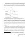
shown in Figure 6.1 a). Here the detector D is biased by voltage source V and connected to
the input of preamplifier A which has feedback capacitor Cf and feedback resistor Rf.
The output of the preamplifier following the absorption of an γ-ray of energy Ex in
detector D is shown in Figure 6.1 b) as a step of amplitude Vx (on a longer time scale, the
step will decay exponentially back to the baseline, see Section 6.3). When the γ-ray is
absorbed in the detector material it releases an electric charge Qx = Ex/ε, where ε is a material
constant. Qx is integrated onto Cf, to produce the voltage Vx = Qx/Cf = Ex/(εCf). Measuring
the energy Ex of the γ-ray therefore requires a measurement of the voltage step Vx in the
presence of the amplifier noise σ, as indicated in Figure 6.1 b).
Rf
V
Cf
D
A
Preamp Output (mV)
4
2
σ
-2
-4
0.00
a)
Vx
0
b)
0.02
0.04
0.06
Time (ms)
Figure 6.1: a) Charge sensitive preamplifier with RC feedback; b) Output on absorption of an
γ-ray.
Reducing noise in an electrical measurement is accomplished by filtering. Traditional
analog filters use combinations of a differentiation stage and multiple integration stages to
convert the preamp output steps, such as shown in Figure 6.1 b), into either triangular or
semi-Gaussian pulses whose amplitudes (with respect to their baselines) are then
proportional to Vx and thus to the γ-ray’s energy.
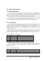
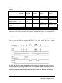
Digital filtering proceeds from a slightly different perspective. Here the signal has been
digitized and is no longer continuous. Instead it is a string of discrete values as shown in
Figure 6.2. Figure 6.2 is actually just a subset of Figure 6.1 b), in which the signal was
digitized by a Tektronix 544 TDS digital oscilloscope at 10 MSA (megasamples/sec). Given
this data set, and some kind of arithmetic processor, the obvious approach to determining Vx
18
DGF-4C User’s Manual V4.03
© XIA 2009. All rights reserved.
is to take some sort of average over the points before the step and subtract it from the value
of the average over the points after the step. That is, as shown in Figure 6.2, averages are
computed over the two regions marked “Length” (the “Gap” region is omitted because the
signal is changing rapidly here), and their difference taken as a measure of Vx. Thus the value
Vx may be found from the equation:
V x ,k = − ∑ WiVi + ∑ WiVi
(6.1)
i ( before )
i ( after )
where the values of the weighting constants Wi determine the type of average being
computed. The sums of the values of the two sets of weights must be individually
normalized.
Preamp Output (mV)
4
2
Length
Gap
0
Length
-2
-4
20
22
24
26
28
30
Time ( μs)
Figure 6.2: Digitized version of the data of Figure 6.1 b) in the step region.
The primary differences between different digital signal processors lie in two areas: what
set of weights { Wi } is used and how the regions are selected for the computation of Eqn. 6.1.
Thus, for example, when larger weighting values are used for the region close to the step
while smaller values are used for the data away from the step, Eqn. 6.1 produces “cusp-like”
filters. When the weighting values are constant, one obtains triangular (if the gap is zero) or
trapezoidal filters. The concept behind cusp-like filters is that, since the points nearest the
step carry the most information about its height, they should be most strongly weighted in the
averaging process. How one chooses the filter lengths results in time variant (the lengths vary
from pulse to pulse) or time invariant (the lengths are the same for all pulses) filters.
Traditional analog filters are time invariant. The concept behind time variant filters is that,
since the γ-rays arrive randomly and the lengths between them vary accordingly, one can
make maximum use of the available information by setting the length to the interpulse
spacing.
19
DGF-4C User’s Manual V4.03
© XIA 2009. All rights reserved.
In principle, the very best filtering is accomplished by using cusp-like weights and time
variant filter length selection. There are serious costs associated with this approach however,
both in terms of computational power required to evaluate the sums in real time and in the
complexity of the electronics required to generate (usually from stored coefficients)
normalized { Wi } sets on a pulse by pulse basis.
The DGF-4C takes a different approach because it was optimized for very high speed
operation. It implements a fixed length filter with all Wi values equal to unity and in fact
computes this sum afresh for each new signal value k. Thus the equation implemented is:
LV x ,k = −
k − L −G
∑Vi +
k
∑V
(6.2)
i
i = k − 2 L −G +1 i = k − L +1
where the filter length is L and the gap is G . The factor L multiplying Vx ,k arises because
the sum of the weights here is not normalized. Accommodating this factor is trivial.
While this relationship is very simple, it is still very effective. In the first place, this is
the digital equivalent of triangular (or trapezoidal if G ≠ 0) filtering which is the analog
industry’s standard for high rate processing. In the second place, one can show theoretically
that if the noise in the signal is white (i.e. Gaussian distributed) above and below the step,
which is typically the case for the short shaping times used for high signal rate processing,
then the average in Eqn. 6.2 actually gives the best estimate of Vx in the least squares sense.
This, of course, is why triangular filtering has been preferred at high rates. Triangular
filtering with time variant filter lengths can, in principle, achieve both somewhat superior
resolution and higher throughputs but comes at the cost of a significantly more complex
circuit and a rate dependent resolution, which is unacceptable for many types of precise
analysis. In practice, XIA’s design has been found to duplicate the energy resolution of the
best analog shapers while approximately doubling their throughput, providing experimental
confirmation of the validity of the approach.
6.2
Trapezoidal Filtering in the DGF-4C
From this point onward, we will only consider trapezoidal filtering as it is implemented
in the DGF-4C according to Eqn. 6.2. The result of applying such a filter with Length L=1μs
and Gap G=0.4μs to a γ-ray event is shown in Figure 6.3. The filter output is clearly
trapezoidal in shape and has a rise time equal to L, a flat top equal to G, and a symmetrical
fall time equal to L. The basewidth, which is a first-order measure of the filter’s noise
reduction properties, is thus 2L+G.
This raises several important points in comparing the noise performance of the DGF-4C
to analog filtering amplifiers. First, semi-Gaussian filters are usually specified by a shaping
time. Their rise time is typically twice this and their pulses are not symmetric so that the
basewidth is about 5.6 times the shaping time or 2.8 times their rise time. Thus a semiGaussian filter typically has a slightly better energy resolution than a triangular filter of the
same rise time because it has a longer filtering time. This is typically accommodated in
amplifiers offering both triangular and semi-Gaussian filtering by stretching the triangular
rise time a bit, so that the true triangular rise time is typically 1.2 times the selected semi-
20
DGF-4C User’s Manual V4.03
© XIA 2009. All rights reserved.
Gaussian rise time. This also leads to an apparent advantage for the analog system when its
energy resolution is compared to a digital system with the same nominal rise time.
One important characteristic of a digitally shaped trapezoidal pulse is its extremely sharp
termination on completion of the basewidth 2L+G. This may be compared to analog filtered
pulses whose tails may persist up to 40% of the rise time, a phenomenon due to the finite
bandwidth of the analog filter. As we shall see below, this sharp termination gives the digital
filter a definite rate advantage in pileup free throughput.
ADC output
Filter Output
3
ADC units
33x10
32
31
G
L
2L+G
30
9.5
10.0
10.5
11.0
Time
11.5
12.0
12.5µs
Figure 6.3: Trapezoidal filtering of a preamplifier step with L=1μs and G=0.4μs.
6.3
Baselines and preamplifier decay times
Figure 6.4 shows an event over a longer time interval and how the filter treats the
preamplifier noise in regions when no γ-ray pulses are present. As may be seen the effect of
the filter is to reduce both the amplitude of the fluctuations and their high frequency content.
This signal is termed the baseline because it establishes the reference level from which the γray peak amplitude Vx is to be measured. The fluctuations in the baseline have a standard
deviation σe which is referred to as the electronic noise of the system, a number which
depends on the rise time of the filter used. Riding on top of this noise, the γ-ray peaks
contribute an additional noise term, the Fano noise, which arises from statistical fluctuations
in the amount of charge Qx produced when the γ-ray is absorbed in the detector. This Fano
noise σf adds in quadrature with the electronic noise, so that the total noise σt in measuring
Vx is found from
σt = sqrt( σf2 + σe2)
(6.3)
The Fano noise is only a property of the detector material. The electronic noise, on the
other hand, may have contributions from both the preamplifier and the amplifier. When the
21
DGF-4C User’s Manual V4.03
© XIA 2009. All rights reserved.
preamplifier and amplifier are both well designed and well matched, however, the amplifier’s
noise contribution should be essentially negligible. Achieving this in the mixed analog-digital
environment of a digital pulse processor is a non-trivial task, however.
3
33x10
σt
32
ADC units
ADC Output
Filter Output
31
30
Vx
σe
29
28
75
80
85
90
95µs
Time
Figure 6.4: A γ-ray event displayed over a longer time period to show baseline noise and the
effect of preamplifier decay time.
With a RC-type preamplifier, the slope of the preamplifier is rarely zero. Every step
decays exponentially back to the DC level of the preamplifier. During such a decay, the
baselines are obviously not zero. This can be seen in Figure 6.4, where the filter output
during the exponential decay after the pulse is below the initial level. Note also that the flat
top region is sloped downwards.
Using the decay constant τ, the baselines can be mapped back to the DC level. This
allows precise determination of γ-ray energies, even if the pulse sits on the falling slope of a
previous pulse. The value of τ, being a characteristic of the preamplifier, has to be
determined by the user and host software and downloaded to the module.
6.4
Thresholds and Pile-up Inspection
As noted above, we wish to capture a value of Vx for each γ-ray detected and use these
values to construct a spectrum. This process is also significantly different between digital and
analog systems. In the analog system the peak value must be “captured” into an analog
storage device, usually a capacitor, and “held” until it is digitized. Then the digital value is
used to update a memory location to build the desired spectrum. During this analog to digital
conversion process the system is dead to other events, which can severely reduce system
throughput. Even single channel analyzer systems introduce significant deadtime at this stage
22
DGF-4C User’s Manual V4.03
© XIA 2009. All rights reserved.
since they must wait some period (typically a few microseconds) to determine whether or not
the window condition is satisfied.
Digital systems are much more efficient in this regard, since the values output by the
filter are already digital values. All that is required is to take the filter sums, reconstruct the
energy Vx, and add it to the spectrum. In the DGF-4C, the filter sums are continuously
updated by the FPGA (see Section 5.2), and only have to be read out by the DSP when an
event occurs. Reconstructing the energy and incrementing the spectrum is done by the DSP,
so that the FPGA is ready to take new data immediately after the readout. This usually takes
much less than one filter rise time, so that no system deadtime is produced by a “capture and
store” operation. This is a significant source of the enhanced throughput found in digital
systems.
3
32x10
ADC Output
Fast Filter Output
Slow Filter Output
31
ADC units
30
29
28
Sampling Time
Arrival Time
27
Threshold
26
44
45
46
47
48µs
Time
Figure 6.5: Peak detection and sampling in the DGF-4C.
The peak detection and sampling in the DGF-4C is handled as indicated in Figure 6.5.
Two trapezoidal filters are implemented, a fast filter and a slow filter. The fast filter is used
to detect the arrival of γ-rays, the slow filter is used for the measurement of Vx, with reduced
noise at longer filter rise times. The fast filter has a filter length Lf = 0.1μs and a gap
Gf =0.1μs. The slow filter has Ls = 1.2μs and Gs = 0.35μs.
The arrival of the γ-ray step (in the preamplifier output) is detected by digitally
comparing the fast filter output to THRESHOLD, a digital constant set by the user. Crossing
the threshold starts a counter to count PEAKSAMP clock cycles to arrive at the appropriate
time to sample the value of the slow filter. Because the digital filtering processes are
deterministic, PEAKSAMP depends only on the values of the fast and slow filter constants
and the rise time of the preamplifier pulses. The slow filter value captured following
PEAKSAMP is then the slow digital filter’s estimate of Vx.
23
DGF-4C User’s Manual V4.03
© XIA 2009. All rights reserved.
3
36x10
3
34
2
1
32
ADC units
ADC Output
30
28
26
24
Slow Filter Output
22
Fast Filter Output
PeakSep
20
56
58
60
62
Time
64
66
68µs
Figure 6.6: A sequence of 3 γ-ray pulses separated by various intervals to show the origin of
pileup and demonstrate how it is detected by the DGF-4C.
The value Vx captured will only be a valid measure of the associated γ-ray’s energy
provided that the filtered pulse is sufficiently well separated in time from its preceding and
succeeding neighbor pulses so that their peak amplitudes are not distorted by the action of the
trapezoidal filter. That is, if the pulse is not piled up. The relevant issues may be understood
by reference to Figure 6.6, which shows 3 γ-rays arriving separated by various intervals. The
fast filter has a filter length Lf = 0.1μs and a gap Gf =0.1μs. The slow filter has Ls = 1.2μs
and Gs = 0.35μs.
Because the trapezoidal filter is a linear filter, its output for a series of pulses is the linear
sum of its outputs for the individual members in the series. Pileup occurs when the rising
edge of one pulse lies under the peak (specifically the sampling point) of its neighbor. Thus,
in Figure 6.6, peaks 1 and 2 are sufficiently well separated so that the leading edge of peak 2
falls after the peak of pulse 1. Because the trapezoidal filter function is symmetrical, this also
means that pulse 1’s trailing edge also does not fall under the peak of pulse 2. For this to be
true, the two pulses must be separated by at least an interval of L + G. Peaks 2 and 3, which
are separated by less than 1.0 μs, are thus seen to pileup in the present example with a 1.2 μs
rise time.
This leads to an important point: whether pulses suffer slow pileup depends critically on
the rise time of the filter being used. The amount of pileup which occurs at a given average
signal rate will increase with longer rise times.
Because the fast filter rise time is only 0.1 μs, these γ-ray pulses do not pileup in the fast
filter channel. The DGF-4C can therefore test for slow channel pileup by measuring the fast
filter for the interval PEAKSEP after a pulse arrival time. If no second pulse occurs in this
interval, then there is no trailing edge pileup. PEAKSEP is usually set to a value close to L +
G + 1. Pulse 1 passes this test, as shown in Figure 6.6. Pulse 2, however, fails the PEAKSEP
24
DGF-4C User’s Manual V4.03
© XIA 2009. All rights reserved.
test because pulse 3 follows less than 1.0 μs. Notice, by the symmetry of the trapezoidal
filter, if pulse 2 is rejected because of pulse 3, then pulse 3 is similarly rejected because of
pulse 2.
6.5
Filter decimation
To accommodate the wide range of filter rise times from 0.1μs to 44μs, the filters are
implemented in the FPGA with different clock decimation (filter ranges). The ADC sampling
rate is always 12.5ns, but in higher clock decimations, several ADC samples are averaged
before entering the filtering logic. In decimation 1, 21 samples are averaged, 22 samples in
decimation 2, and so on. Since the sum of rise time and flat top is limited to 31 decimated
clock cycles, filter time granularity and filter time limits are listed in Table 6.1.
Table 6.1: RTPU clock decimations and filter time granularity.
Decimation
1
2
3
4
5
6
Filter granularity
[μs]
0.025
0.05
0.1
0.2
0.4
0.8
max. Trise+Tflat
[μs]
3.175
6.35
12.7
25.4
50.8
101.6
min. Trise
[μs]
0.05
0.1
0.2
0.4
0.8
1.6
min. Tflat
[μs]
0.075
0.15
0.3
0.6
1.2
2.4
All the decimations are implemented in the same FPGA configurations, so the same file can
be downloaded at all times.
6.6
Dead Time and Run Statistics
6.6.1 Definition of dead times
Dead time in the DGF-4C data acquisition can occur at several processing stages. For the
purpose of this document, we distinguish three types of dead time, each with a number of
contributions from different processes.
6.6.1.1 Dead time associated with each pulse
1. Filter dead time
At the most fundamental level, the energy filter implemented in the FPGA requires a
certain amount of pulse waveform (the “filter time”) to measure the energy. Once a rising
edge of a pulse is detected at time T0, the FPGA computes three filter sums using the
waveform data from T- (a energy filter rise time before T0) to T1 (a flat top time plus filter
rise time after T0), see section 6.4 and figure 6.7. If a second pulse occurs during this time,
the energy measurement will be incorrect. Therefore, processing in the FPGA includes pileup
rejection which enforces a minimum distance between pulses and validates a pulse for
recording only if a no more than one pulse occurred from T0 to T1 (in the previous firmware,
T- to T1). Consequently, each pulse creates a dead time Td = (T1 – T0) equal to the filter
time. This dead time, simply given by the time to measure the pulse height, is unavoidable
25
DGF-4C User’s Manual V4.03
© XIA 2009. All rights reserved.
unless pulse height measurements are allowed to overlap (which would produce false
results).
Assuming randomly occurring pulses, the effect of dead time on the output count rate is
governed by Poisson statistics for paralyzable systems with pileup rejection1. This means the
output count rate OCR (valid pulses) is a function of filter dead time Td and input count rate
ICR given by
OCR = ICR * exp(-ICR* 2 * Td),
(6.4)
which reaches a maximum OCRmax = ICRmax/e at ICRmax = 1/(2*Td). Simply speaking, the
factor 2 for Td comes from the fact that not only is an event E2 invalid when it falls into the
dead time of a previous event E1, but E1 is rejected as piled up as well.
Fig. 6.7. Pulse dead time without trace capture. A second pulse arriving at T1+x will pass pileup
inspection at time T4+x. No dead time is incurred for the FPGA readout if it is completed at a
time T3 before T4 (T4-T1 = T1-T0, the filter dead time). The FIFO dead time is ignored.
As a consequence of the pileup inspection, there is a delay of one filter time between the
rising edge of the pulse and the decision to record the data, i.e. the validation as not piled up.
This delay can be used to pipeline the subsequent processing steps: the coincidence window
and FPGA readout of a first pulse can overlap with the pileup inspection of a second pulse, as
described below.
2. FIFO dead time
The second unavoidable dead time comes from the waveform capture FIFO. When the
user requires waveform data from before time T0, the FIFO must contain this pre-trigger data
at time T0, else the event data is incomplete and the event is rejected. This means that
whenever the FIFO write process was stopped, it takes a pre-trigger time to refresh the pretrigger data and be ready for new events. To minimize this effect, the FIFO write process is
1
G. Knoll, Radiation and Measurement, J Wiley & Sons, Inc, 2000, chapters 4 and 17.
26
DGF-4C User’s Manual V4.03
© XIA 2009. All rights reserved.
stopped only in two cases, when it is necessary to avoid overwriting potentially valid data: a)
When the event validation takes longer than the time available in the FIFO (12.8 μs minus
the pre-trigger time) and b) when the readout of a valid event by the DSP is not completed
before the FIFO is filled. In the new firmware, the impact of case b) is practically eliminated
by restarting the FIFO write process before the DSP readout is finished, overwriting data
already read with fresh pre-trigger data. (4 writes can be performed for one read, and the
writing is resumed after ¾ of the waveform is read)
In the current firmware implementation, the FIFO logic does not allow the post-trigger
data of a second pulse to be stored while a first pulse is waiting for readout. This means if
waveforms are requested, overlap of a second pulse with the FPGA readout is not possible
because the waveform data of the second pulse can not be recorded. Essentially the FIFO is
dead for new events until the FPGA readout is complete. This effect is usually more
significant than the cases a) and b) above, at least for systems like HPGe detectors and
scintillators where the filter time (typically 2-6 μs) is well below the FIFO limit of 12.8 μs
minus the pre-trigger time.
In any case, the FIFO dead time from a) and b) and the FIFO’s effect to prevent overlap
of a second pulse with the FPGA readout is only in effect when waveforms are required by
the user, i.e only in list mode runs with non-zero tracelengths.
Fig. 6.8. Pulse dead time with trace capture. The FIFO blocks new events as long there is a valid
event in the FPGA. Therefore the soonest arrival time for a second pulse is at T3 after the
FPGA readout is complete (now later than T4). The FIFO write resumes before T3, overwriting
data already read out, and thus contains pre-trigger data for the second pulse at T3.
27
DGF-4C User’s Manual V4.03
© XIA 2009. All rights reserved.
3. Coincidence window
Each valid event is further subject to a coincidence test, i.e. checking the hit pattern
against the user defined pattern of acceptable events. The test itself requires about 12 clock
cycles overhead plus a minimum window of 1 clock cycle and thus adds about 160 ns of
dead time. Any time added by the user to the coincidence window increases the dead time
accordingly. However, the full dead time is only incurred by the first channel that is
validated, since the coincidence window is counted from the first event validation. For
example, if a second channel sees no pulse during the coincidence window, it will be active
during the full coincidence window. If a third channel sees a pulse and is validated by
passing its local pileup inspection 500ns after the first, it was active for 500 ns longer than
the first channel and incurred dead time of (coincidence window – 500ns). Similar to the
FPGA readout described below, the coincidence window may overlap with the pileup
inspection of a subsequent pulse, so it only adds to dead time if FPGA readout and
coincidence window combined are longer that the filter time.
4. FPGA readout dead time
The current firmware only allows valid data of one event at a time in the FPGA. The
DSP reads out the data after receiving an event interrupt if the coincidence test was passed.
Thus once an event is validated, the channel may incur dead time until the DSP finishes the
data readout of hit pattern, energy filter sums, and possibly waveforms. However, the pileup
inspection of a subsequent pulse can already begin while the first event is read out, as long as
it finishes after the DSP has completed the readout. This means the DSP has a filter time
(minus coincidence window) available for readout. The readout creates additional dead time
only if it exceeds this time. For typical HPGe filter settings with no traces and minimum
coincidence window, the FPGA readout time usually fulfils this requirement and thus
introduces no additional dead time.
However, when traces are required, the FIFO logic does not allow the post-trigger data
of a second pulse to be stored until the readout is completed, so in this case the readout
always creates dead time equal to the full readout time. Details are as follows:
a) Hit pattern readout
At the beginning of the readout, the DSP reads the hit pattern and determines which
channel to read. This, together with some general overhead, takes about 1-2
microseconds.
b) filter sum readout
Readout of filter sums takes about 1-2 microseconds per channel marked in the hit
pattern. (get exact numbers from DSP code for MCA and list mode).
c) waveform readout
Waveform readout occurs in the same processing step as the filter sum readout and
increases the DSP readout time by 4x the recorded waveform length. <to be improved
with P500 addressing scheme and fewer waitstates> It can be avoided by setting the
requested waveform length to zero. Note that if the waveform length is nonzero,
waveforms are still read in the “compressed” run types 0x101-103 for possible pulse
shape analysis, only the storing of waveforms in the output data stream is disabled. In
MCA runs, waveforms are never read, so the waveform length is irrelevant.
28
DGF-4C User’s Manual V4.03
© XIA 2009. All rights reserved.
In the current firmware, the FPGAs are released to resume data acquisition only after all
channels marked in the hit pattern have been read out. At this time, all channels are cleared
after readout, which means that pulses validated after the end of the coincidence window
(and thus not contributing to the hit pattern) are lost. The readout therefore causes dead time
in all other channels in the module as well.
5. Fast trigger dead time (FTDT)
Fig. 6.9. Fast Trigger Dead Time (FTDT). A second pulse is not detected if the trigger filter
output is still above threshold.
An additional type of dead time only affects the trigger filter. Triggers are issued when
the trigger filter output goes above the trigger threshold set by the user. However, depending
on the length of the trigger filter and the rise time of the input signal, the trigger filter output
will remain above threshold for a finite amount of time. During this time, no second trigger
can be issued2. Therefore triggers are not counted during this time, and when computing the
input count rate, the time lost has to be taken into account. FTDT is thus purely a correction
for the computation of the input count rate.
6. Summary
As listed in Table 6.2, the dead time associated with each pulse is essentially in the order
of the filter dead time, unless waveforms are requested by the user. Even with waveforms,
few counts are lost at low count rates for short waveforms. Losses are significant with longer
waveforms or at higher count rates. To some extend, this is due to the general purpose FIFO
logic which allows waveforms up to the maximum available memory in the FPGA. For
application where only short traces are required, lower dead times are possibly by
reorganizing memory to buffer multiple events in the FPGA. Please contact XIA for details.
2
The MAXWIDTH parameter can be used to define a maximum acceptable time over threshold and thus to
reject events piled up “on the rising edge”.
29
DGF-4C User’s Manual V4.03
© XIA 2009. All rights reserved.
Table 6.2 Examples of dead times in typical conditions. Assumes events with only one active
channel.
MCA run,
2μs filter,
any ICR
MCA run,
6μs filter,
any ICR
A: Filter dead time
2 μs
6 μs
LM run,
6μs filter,
no trace,
ICR = 1k/s
6 μs
B: FIFO dead time1
--
--
--
C: Coinc. Window
0.2 μs
0.2 μs
0.2 μs
D: FPGA readout
3 μs
3 μs
3 μs
max(A,B+C)
max(A,B+C)
max(A,B+C)
SFDT per event
(= Td)
OCR
Fraction events lost
= 3.2 μs
= 6 μs
ICR * e(-ICR* 2 * Td)
1-e(-ICR* 2 * Td)
= 6 μs
988/s
1.2%
LM run,
6μs filter,
2μs trace,
ICR = 1k/s
6 μs
C + D + 0us
(write not stopped)
0.2 μs
3 μs +4 x 2 μs
= 11 μs
A+B
(B includes C,D)
= 17.2 μs
966/s
3.4%
LM run,
6μs filter,
2μs trace,
ICR = 10k/s
6 μs
C + D + 0us
(write not stopped)
0.2 μs
3 μs +4 x 2 μs
= 11 μs
A+B
(B includes C,D)
= 17.2 μs
7089/s
29%
Note: 1. FIFO logic prevents overlap of second pulse with coincidence window and FPGA
readout, but only when waveforms are requested. Additional dead time due to stopped FIFO
write process occurs only when filter dead time > 12.8 μs – pre-trigger time
6.6.1.2 Dead time associated with external conditions
There are three dead time effects that originate from outside the trigger/filter FPGA. The
first two have the effect of stopping the DGF-4C live time counter, the last is counted
separately.
Fig. 6.10. The live time counter is stopped when the signal is out of range and when events are
rejected because of a processing backlog in the DSP or spectrum memory increment process in
the FPGA. SFDT and FTDT are only counted when the live time is on. The gate dead time is
counted in a separate counter, but also only when the live time is on. Run time and total time
are always on unless the run is stopped (see below).
30
DGF-4C User’s Manual V4.03
© XIA 2009. All rights reserved.
1. Signal out of range
When detector gains or offsets drift, or an unusual large pulse is generated in the
detector, the analog input of the ADC may go out of range. In this condition, the FPGA can
not accumulate meaningful filter sums and thus is considered dead. This dead time is
enforced during the actual out-of-range condition and several filter times afterwards until the
bad ADC samples are purged from filter memory. The live time counter is stopped during the
out-of-range condition because no triggers can be issued and no pulses are counted.
2. On-board pulse processing overload
Processing dead time includes all time lost in the acquisition due to the conversion of the
raw energy filter sums into the pulse height which is stored in list mode memory and/or
binned into spectrum memory. This conversion process begins after the raw filter sums have
been read out from the FPGA. The FPGA resumes its acquisition after the readout and raw
filter sums for several hundred events can be buffered in DSP memory. Therefore the
computation of the pulse height in the DSP incurs no dead time as long as a) average count
rates are below the maximum DSP processing rate and b) bursts of pulses do not fill the raw
data buffer faster than the DSP can process it.
The maximum processing rate depends on the multiplicity of the event and whether
pulse shape analysis is performed on the waveforms. For standard processing as in MCA
runs, it is about 240-480,000 pulses/s, i.e. the DSP spends roughly 2-4 μs per pulse to
compute the energy. (Processing events containing pulses from several channels has less
overhead and is thus faster per pulse.) This rate is much higher than the maximum throughput
set by Poisson statistics for most typical filter times.
The size of the raw data buffer is 8k words in mode 0x100, else about 4k words. An
event without waveforms, consisting of 1-4 pulses from the 4 channels of a module, contains
9-12 raw data words per pulse (depending on the number of channels contributing). This
means up to ~400 events can be stored in the raw buffer, and it does not matter how closely
they follow each other as long as on average, the DSP can keep up with the processing. For
the standard processing in MCA runs as above, the time to process a pulses is about 2-4 μs.
Therefore, no events are lost if for example the 400 pulses occur in 400 μs followed by a
pause of 400-1200 μs (i.e. 1M/s bursts with a duty cycle of 50-25%) or in 200 μs followed by
a pause of 600-1400 μs (2M/s bursts with a duty cycle of 25-12.5%), and so on.
However, if waveforms are read and pulses contain more raw data words, the raw buffer can
contain correspondingly fewer events. For example, when collecting 1.875 μs waveforms, a
pulse consists of ~160 words and thus there is only room for ~25 pulses. Assuming no pulse
shape analysis, the time to process a pulse is again roughly 2-4 μs. Thus the buffering limit
changes from less than 400 pulses in ~800-1600 μs to less than 25 pulses in 50-200 μs.
Obviously, the average rate stays the same, but the length of bursts is reduced.
In any case, burst rates are still limited by Poisson statistics (filter dead time) and the FPGA
readout time, if it exceeds the filter time or waveforms are read.
3. VETO and GFLT
If an external signal prohibits acquisition using the GFLT or VETO signals, the channel
is also dead (though on purpose). As further described in section 7.5, the use of these signals
may depend on the application:
31
DGF-4C User’s Manual V4.03
© XIA 2009. All rights reserved.
a) On one hand they may be used to reject an individual pulse (e.g. externally
summing multiplicities from several channels and issuing a short validation pulse
at the right time in the validation process). In this case the actual length of the
pulse does not correspond to a dead time. The GFLT input is set up for this
purpose.
b) On the other hand GFLT or VETO may block validation of events for certain
amounts of time (e.g. changing sources or [de]activating beams). In this case they
should be counted clock cycle by clock cycle as dead time. Both the VETO and
the GFLT inputs are available for this purpose, GFLT as a global signal for the
whole system, VETO as a dedicated signal for each channel. GFLT acts at the
time of pulse validation, VETO acts at the time of the rising edge of the pulse.
However, the GFLT input can be routed to replace the VETO input with a user
option.
The appropriate way to count GFLT or VETO dead time may thus depend on the
experiment. See below (GDT) for the current method implemented in the firmware.
6.6.1.3 Dead time associated with host readout
Fig. 6.11 After a run start command arrives from the host at T0, the DGF-4C module acquires
several buffers of data (T1-T2, T3-T4) until the external memory is full and is read out by the
host at T5. (For single buffer mode not using external memory, the transfer is replaced by a
host readout, which however takes much longer.)
The final type of dead time comes from the readout of data from DGF-4C memory to the
host PC. In MCA mode, this is limited to the access arbitration for the spectrum memory.
The memory has only a single port for both the increments according to the pulse height
computed by the DSP and for readout to the host PC, arbitrated by an FPGA. While the host
is reading the memory, spectrum increments are queued in a buffer (2K long). At maximum
count rate, it will take the DSP at least (2K * processing time) to fill the buffer and
correspondingly longer at lower count rates, while the host readout typically takes ~30 ms.
Thus host readout dead time is usually not an issue in MCA runs unless spectra are read very
frequently.
32
DGF-4C User’s Manual V4.03
© XIA 2009. All rights reserved.
In list mode runs, the DGF-4C memory fills up after a certain number of events are
acquired. Acquisition is stopped until the memory is read out. Depending on the “buffer per
spill” setting, this is organized in one of three ways:
a) In single buffer mode, acquisition stops after the DSP’s 8K buffer is filled and data is
read out in a slow transfer mode.
b) In 32 buffer mode, the 8K buffer is automatically transferred to external memory.
The transfer incurs about 550µs dead time (this may be improved in the future).
After 32 transfers, the external memory is full and acquisition is stopped. The
external memory is read out in a fast block transfer that takes about 30 ms
c) In 16/16 buffer mode (or double buffer mode), the 8K buffer is also automatically
transferred to external memory, but only 16 times. Then a flag is raised so that the
host can read out the memory in a fast block transfer while acquisition continues and
new data is stored in the second half of the memory. However, since again the
memory has only a single port, host readout can not happen at the same time as the
DSP transfer. Normally, the readout will be finished before the DSP 8K buffer is
filled, but at high count rate or when recording waveforms, the transfer may have to
wait until the host finished reading the external memory, which means the
acquisition is stopped and there will be dead time in addition to the ~550 us transfer
time.
Case b) is pictured in Fig. 6.11; the difference for case c) is shown with the dashed lines.
The Pixie-4 acquires several buffers of data (T1-T2, T3-T4) until the external memory is full
and read out by the host at T5. After readout, a second spill resumes at T6. The live time
counter is active while events can be acquired, which excludes memory transfer and readout.
The run time starts a bit earlier and lasts a bit longer than the live time for each buffer, and
does not switch off for out-of range or other conditions. The total time counts all time from
T0 to the end of the last spill. The Pixie 4 can not count the time between the user clicking a
“start run” button in the interface and T0. In case c), the acquisition resumes already at T5
while the memory is read out independently. In a) and b), there is thus dead time in the Pixie4 while it is waiting for the host to read out the data. In b) and c) there is dead time while the
data is transferred to external memory. In all cases, the run is considered stopped in the Pixie4, as opposed to the dead times described in section 6.6.1.2. The readout dead times are
omitted from the Pixie-4 live time and run time counters (counters are stopped), but included
in the “total time” counter.
Examples of host readout dead times are shown in Table 6.3. Rows A and B are copied
from Table 6.2 for comparison. When no traces are recorded, the fraction of time lost to
readout is less than 1% even up to moderately high count rates; and well below the fraction
of events lost due to Td (dominated by the filter time). When traces are recorded, the fraction
of time lost increases, but is still below the fraction of events lost due to Td.
33
DGF-4C User’s Manual V4.03
© XIA 2009. All rights reserved.
Table 6.3. Dead times from host readout in 32 buffer/spill mode. (One channel active per event)
(recompute for USB)
A: OCR
B: Fraction events lost
to Td (from table 6.2)
C: Events in buffer
(8K / Nwords)
D: Buffer fill time
=C/A
E: EM fill time
= 32 x (D + 0.55ms)
F: Total readout time
= (32x 0.55 +30)ms
~ TT-LT per spill
Fraction time lost to
readout = F/(E+30ms)
LM run 0x103,
6μs filter,
no trace,
ICR = 1k/s
988/s
1.2%
LM run 0x103,
6μs filter,
no trace,
ICR = 10k/s
8869/s
11.3%
LM run 0x100,
6μs filter,
no trace,
ICR = 1k/s
988/s
1.2%
LM run 0x100,
6μs filter,
2μs trace,
ICR = 1k/s
966/s
3.4%
LM run 0x100,
6μs filter,
2μs trace,
ICR = 10k/s
7099/s
29%
1637
1637
682
50
50
1.657 s
0.185 s
0.690 s
51.8 ms
7.0ms
53.042 s
5.938 s
22.098 s
1.675 s
0.242 s
47.6ms
47.6ms
47.6ms
47.6ms
47.6ms
<0.1%
0.8%
0.2%
2.8%
19.7%
6.6.2 Live and dead time counters
The DGF-4C firmware has been optimized to reduce the dead time as much as possible,
and a number of counters measure the remaining dead times as well as the number of counts
to provide information for dead time correction. The result of these counters is stored in the
following DSP output variables:
TOTAL TIME
The TOTAL TIME is an attempt to measure the real laboratory time during which the
DGF-4C module was requested to take data. It essentially counts the time from the most
recent command to start a new run, i.e. in list mode runs the start of the first spill. The
TOTAL TIME includes the time spent for run start initialization and host readout. Thus it can
be used together with the LIVE TIME to determine the fraction of the real time the module
was actively taking data. However, since it is based on the DGF-4C’s internal oscillator (a
part with 50 ppm accuracy from module to module), it may not be as precise as a “laboratory
wall clock” over long time spans (e.g. the host PC’s internal clock). Also, it does not take
into account the time required to send commands from the PC to the module.
RUN TIME
The RUN TIME variable gives the time during which the DSP on the DGF-4C module
was “switched on” for data acquisition. The usefulness of this variable is very limited. It is
less than the real time passed in the laboratory during acquisition (e.g. the TOTAL TIME or
the time measured by the host PC) because it omits the time for a) start run signals from the
PC to reach the DSP, b) communication between modules to synchronize the run start, c)
clearing of memory and output variables before starting a run, and d) time spent waiting for
readout. It is larger than the time the FPGA is ready to take data because it does not account
for the dead time from filter, FIFO, or DSP readout. Thus for most purposes, the LIVE
TIME, TOTAL TIME, or the host PC’s real time (not the DSP variable named REAL TIME)
34
DGF-4C User’s Manual V4.03
© XIA 2009. All rights reserved.
are more appropriate. This variable is provided mainly to provide backwards compatibility to
previous software revisions.
LIVE TIME
The LIVE TIME is counted in the FPGA independently for each channel and measures
the time the channel is ready for acquisition. The LIVE TIME counter starts when the DSP
finished all setup routines at the beginning of a run, omits the times the ADC signal is out of
range or overloaded with processing (section 6.6.1.2, 1. and 2.), and ends when the DSP
encounters an end run condition (e.g. memory full or host stop). Subsequent spills add in the
same way. It is thus the time during which triggers are counted and can cause recording (or
pile up) of data, the best available measurement of the time the channel was active.
FTDT (fast trigger dead time)
The fast trigger dead time counts the time the trigger filter is unable to issue triggers
because the trigger filter output is already above threshold (and can not recognize a second
pulse). It does not include the time triggers have been “paused” for a short time after a first
trigger (an advanced user option to suppress double triggering), because the concept is that
all triggers occurring during the pause are counted as only one trigger. When computing the
input count rate, one should divide the number of triggers counted (FASTPEAKS) by the
difference (LIVE TIME – FTDT) since triggers are not counted during FTDT.
SFDT (slow filter dead time)
The slow filter dead time counts the time new triggers will not lead to the recording of
new data. This includes effects 1-4 listed in section 6.6.1.1 as dead time associated with a
pulse. In detail,
a) it includes the time the pileup inspection is taking place and the summation of
energy filter sums is in progress,
b) it includes the time the FIFO does not contain fresh pre-trigger data or is unable
to accept a new event
c) it includes the time from event validation until one filter time before the end of
the DSP readout. This includes DSP readout of an event in a different channel
after which data in all channels are discarded. (the end of dead time counting
before the end of the DSP readout is implemented as a delayed start of the
counting)
GDT (GATE dead time)
The dead time from VETO or GFLT is counted separately from SFDT for each channel.
As mentioned above and further described in section 7.5, the use of these signals may depend
on the application.
In the current firmware, a rising (or optionally falling) edge at the VETO input creates a
GATE PULSE with length GATE WINDOW (see section 7.5). Both this GATE PULSE and
the (optionally inverted) signal on the GFLT input are counted as GDT clock cycle by clock
cycle. If at least one of them is high, GDT is incremented. If the GFLT input is unused but
defaults to high so that GDT is equal to the live time, invert the GFLT polarity to only count
the GATE PULSE time. The GFLT input can be used instead of the VETO input, and if this
35
DGF-4C User’s Manual V4.03
© XIA 2009. All rights reserved.
option is used only the GATE PULSE derived from the GFLT input is counted, not the
original GFLT.
For the case that the GFLT input is used for the above described validation pulses, it
may be more useful to work with the number of pulses issued. They can be counted by using
the GFLT input as the source for GATE PULSEs, which are counted in the variable
GCOUNT.
6.6.3 Count rates
Besides the live and dead times, the DGF-4C counts the numbers of triggers in each
channel, FASTPEAKS, the number of valid events with one or more channels,
NUMEVENTS, and the number of valid pulses processed for each channel, NOUT. In
addition, it counts the number of gate pulses for each channel, GCOUNT. FASTPEAKS and
GCOUNT are inhibited when the live time is not counted. NUMEVENTS and NOUT by
nature only count events captured when the live time is not counted.
Count rates are then computed in the C library as follows:
Input count rate
ICR = FASTPEAKS / (LIVE TIME – FTDT)
Event rate
ER
= NUMEVENTS / RUN TIME
Channel output count rate
OCR = NOUT / LIVE TIME
Gate count rate
GCR = GCOUNT / LIVE TIME
Users are free to use the reported values to compute rates and time better matching their
preferred definitions.
Fig. 6.12 OCR and Livetime fractions of FTDT and SFDT as a function of ICR in a
measurement with a random pulse generator. The measured OCR follows the expected
behavior from Eq. (6.4) with a fit value of Td very close to the pileup inspection time (energy
filter rise time plus energy filter flat top plus a few cycles). Measurement taken with Pixie-4
Note: Output pulse counters are updated whenever an event has been processed; input,
gate and all time counters are updated every ~7ms. Therefore reading rates at random times,
e.g. clicking Update in the DGF Viewer, might return slight inconsistencies between input
36
DGF-4C User’s Manual V4.03
© XIA 2009. All rights reserved.
rates and output rates. At the end of the run, all rates are updated and these effects should
disappear.
37
DGF-4C User’s Manual V4.03
© XIA 2009. All rights reserved.
7 Operating multiple DGF-4C modules synchronously
When many DGF-4C modules are operating as a system, it may be required to
synchronize clocks and timers between them and to distribute triggers across modules. It will
also be necessary to ensure that runs are started and stopped synchronously in all modules.
To distribute clocks and triggers it is necessary to connect the modules together via the
back plane bus. In a revision-D DGF system there will be a clock master on one end of the
bus, a number of slaves, and the clock terminator at the far end of the bus. In a revision-E
DGF system there will be a clock master on the far right side of the bus and a number of
clock repeaters, but no slave modules. The bus is a positive ECL (PECL) bus, which needs to
be terminated properly by installing the appropriate jumpers or setting the FET switches
through the software. All jumpers associated with the auxiliary bus are located near the 16pin connector at the back of the board.
Note: if several modules are in a CAMAC crate, you have to initialize all modules, even
if you work with only one of them. A module that is not initialized can disturb CAMAC
communication, even if it is not specifically addressed.
7.1
Multiplicity unit
The outputs from the digital leading edge discriminators, called fast triggers elsewhere in
this document, are summed together in the multiplicity unit to produce a positive multiplicity
signal at the MultOut front panel connector. When terminated into 50Ω, its amplitude is
35 mV per trigger. The pulse width can be adjusted for each channel independently via the
variable “Pulse width” on the Channel CSRA Edit Panel of the DGF-4C viewer. The default
is 4 which translates into a width of 4 * 12.5 ns = 50 ns. Through the MultIn front panel input
you can add the multiplicity signal of another unit to the current sum. This way it is possible
to daisy chain many modules to build up multiplicity sums. The signal delay per module is
about 5-10ns. If precise timing is required for larger groups of modules, connections should
be made in parallel to an external summing unit, rather than daisy chaining the modules.
7.2
Clock distribution
Clocks are distributed via the backplane connector and/or the 4-pin Firewire connector at
the back of the board. Depending of the module revision, connections can be made either by
a continuous flat cable or by module-to module jumper cables, as detailed below. The
distributed clock is always 40 MHz. On Rev. F modules, the clock is doubled in the FPGA
and DSP.
7.2.1 Clock distribution for revision-D modules
When jumpers JP1 and JP2 are installed, the local 40 MHz clock is fed into the board
circuitry. Jumpers JP5 and JP6 connect the clock lines of the bus to 100Ω termination
resistors. The recommended jumper settings for master, middle, and terminator modules are:
38
DGF-4C User’s Manual V4.03
© XIA 2009. All rights reserved.
Table 7.1: On-board jumper settings for the clock distribution on Rev. D modules.
Module
Master
Middle (slave)
Terminator
Standalone
JP1 and JP2
Yes
No
No
Yes
JP3 and JP4
Yes
Yes
Yes
Yes
JP5 and JP6
No
No
Yes
Yes
Clocks are distributed via the 16 pin backplane connector. The connector pins are
organized into two rows. Row-A consists of the even-numbered pins and is the row which is
physically closest to the PC-board. The other row is row-B and consists of the odd-numbered
pins. When inserted into a CAMAC crate the orientation of the connector is such that the
pins 15 and 16 are found at the top end of the connector; row A is to the right. Pins 13 and 15
carry the clock signal on row B, pins 14 and 16 on row A.
The clock lines on row-B are always connected to the differential on-board clock
receivers. The clock lines on row-A can be disconnected via the jumpers JP3,4 (located next
to the connector). It is advised, however, that JP3,4 be set for all DGF-4Cs in a system. The
breaking of the clock bus is of use only in very large systems, where the drive capability of a
single PECL driver may prove insufficient to supply all modules. In this case, an external
clock driver may supply a PECL clock through the 4-pole Firewire connector (on the fire
wire lines 1A and 1B). For the clock master, the Firewire connector can be used as a second
clock output.
The clock connection between Rev. D modules is best made with a continuous flat cable,
together with the trigger lines (see below).
7.2.2 Clock distribution for revision-E modules
When jumpers JP5 is set to “board clock”, and JP1 and JP2 are installed, the local
40 MHz clock is fed into the board circuitry. With JP5 in the “external” position and JP 1,2
removed, the module will use the incoming clock signal from the backplane connector, and
repeat the clock signal to the outgoing lines. Jumpers JP3 and JP4 connect the incoming
clock lines of the bus to 100Ω termination resistors. The recommended jumper settings for
master, middle (repeater), and terminator modules are:
Table 7.2: On-board jumper settings for the clock distribution on Rev. E modules.
Module
Master
Repeater
Terminator
Standalone
FW input
JP1 and JP2
Yes
No
No
Yes
JP3 and JP4
No
Yes
Yes
Yes
JP5
“board clock”
“external”
“external”
“board clock”
Crate Position
Most right
Middle
Most left
Any
No
Yes
“external”
Any
Clocks are distributed via the 16 pin backplane connector. The connector pins are
organized into two rows. Row-A (incoming) consists of the even-numbered pins and is the
row which is physically closest to the PC-board. The other row (outgoing) is row-B and
consists of the odd-numbered pins. When inserted into a CAMAC crate the orientation of the
39
DGF-4C User’s Manual V4.03
© XIA 2009. All rights reserved.
connector is such that the pins 15 and 16 are found at the top end of the connector; row A is
to the right. Pins 13 and 15 carry the clock signal on row B, pins 14 and 16 on row A.
The clock connection between Rev. E modules should be made using 2x jumper cables
from row-B of one module to row-A of the left neighbor. Consequently, the clock master
must be in the most right position, the terminator in the most left position. Unlike in Rev. D
modules, the connector pins are always connected to the differential translators. A 4-pole
Firewire connector provides an alternative clock input (lines 1A and 1B). If the clock signal
is provided through row-A of the backplane bus, the Firewire connector can be used to
branch off the clock signal to a secondary crate.
The outgoing clock signal of the master module is available on both row-A and row-B,
as well as on the 4-pole Firewire connector. This can be used to connect clock signals to a
secondary crate of modules, if necessary. No incoming clock signal is allowed on row-A or
the Firewire connector of the clock master module.
7.2.3 Clock distribution for revision-F modules
The clock distribution on DGF Rev. F and Rev. E is identical; both kinds of modules use
an auxiliary header on the rear to distribute 40 MHz clock signals from slot to slot (or
alternatively use a 4-pin Firewire (FW) connector as input). However, in the DGF Rev. F the
distributed clock is doubled in the FPGAs and DSP on each board to obtain the 80 MHz
sampling and processing frequency. Clock mode and termination jumpers have different PCB
references, but the same function. Jumpers should be set according to module function and
position as follows:
Table 7.3: On-board jumper settings for the clock distribution on Rev. E and F modules.
Module
Clock Master
Clock Repeater
Clock Terminator
Standalone
FW input
E: JP1, JP2
F: JP404, JP405
Yes
No
No
Yes
No
E: JP3, JP4
F: JP406, JP407
No
Yes
Yes
Yes
Yes
E : JP5
F: JP403
“board clock”
“external”
“external”
“board clock”
“external”
Crate Position
Most right
Middle
Most left
Any
Any
7.2.4 Mixed systems (revision-D and revision-E)
Since clock distribution between revision-D modules is limited to about 12-16 modules,
revision-E repeater modules can be interspersed between the revision-D modules to connect
larger groups. The backplane connection should be made with a 16x flat cable, but lines have
to be cut as follows for the repeater to work properly:
To the right of a revision-E repeater module, cut lines 13 and 15,
To the left of a revision-E repeater module, cut lines 14 and 16.
If only one revision-D module is placed between the revision-E repeaters, the connection
can also be made with jumper cables from row-A to row-B; eliminating the need to cut lines.
40
DGF-4C User’s Manual V4.03
© XIA 2009. All rights reserved.
7.3
Trigger Distribution
This section describes how to use local and distributed triggers.
7.3.1 Trigger Distribution Within a Module
Within a module, each channel can be enabled to issue triggers (see Settings tab ->
Channel Register). Two kinds of triggers are distributed: First, a Fast Trigger indicating the
trigger filter just crossed the threshold (detecting the rising edge of a pulse), which is used to
start pileup inspection and to stop the FIFOs for waveform acquisition, among other things.
Second, an Event Trigger indicating that pileup inspection was passed, i.e. validating the
event as acceptable. The Event Trigger also tells the DSP that data is ready for readout in the
Trigger/Filter FPGA.
If channels are put in “group trigger” mode, each trigger enabled channel issues both
kinds of triggers to the central Communication FPGA, which builds an OR of all triggers and
sends it back to all channels. The channels then use the distributed fast triggers and event
triggers instead of their own local triggers to capture data. In this way, one channel can cause
data to be acquired at the same time in all other channels of the trigger group. The DSP then
reads data from all participating channels and stores it as one event record. Each channel,
trigger enabled or not, always also generates a “hit” flag if pileup inspection was passed, and
DSP readout is conditional to this flag.
Even in group trigger mode, some data is captured based on the channel’s local trigger.
For example, the pulse height of a pulse is best determined based on the trigger from the
pulse itself, not from a common group trigger that may be delayed – if several channels in a
group are trigger enabled, always the last fast trigger before the first event trigger in this
event is the one that counts. The following table lists which quantities are based on local or
group trigger in group trigger mode. (If not in group trigger mode, all quantities are based on
local triggers.)
Note that for the trigger timing to be correct, all channels in a trigger group should be set
to the same energy filter rise time and flat top. Furthermore, to capture the energy of delayed
channels, ensure that the coincidence window (see section 7.7) is long enough to include the
maximum expected delay.
Channel
Hit and trigger
enabled
Hit, but not
trigger enabled
Not hit
(no pulse or
pileup)
Energy
Waveform
Timestamp
Based on local trigger
Based on (last) group trigger
Always read out
Based on local trigger
Always read out
Based on (last) group trigger
Always read out
Based on group trigger if
“estimate energy” option
selected, else zero.
Only read if “read
always” option selected
Always read out
Based on (last) group trigger
Based on (last) group trigger
unless “local trigger only”
option selected
Always read out
Based on (last) group trigger
unless “local trigger only”
option selected
Always read out
Based on (last) group trigger
unless “local trigger only”
option selected
Only read if “read always”
option selected
Only read if “read always”
option selected
41
DGF-4C User’s Manual V4.03
© XIA 2009. All rights reserved.
Energy: The pulse height of a pulse is best determined based on the trigger from the
pulse itself, not from a common group trigger that may be delayed. Even if a channel is not
trigger enabled, energy filter values are latched when if the local trigger filter crosses the user
defined threshold (after a delay). The channel is then marked as “hit” for the DSP to read out.
Even channels without “hit” are read out if the “read always” option is set for this
channel. In this case, the channel’s energy is usually reported as zero since there was no valid
local trigger to capture the value of the energy filter. However, since the energy filter is
computed continuously, setting the “estimate energy” option will cause the energy filter
value to be captured based on the (last) group trigger. This might be useful for channels with
occasional very small pulses (below the threshold), or possibly to obtain energy estimates on
piled up pulses.
Note that since the timing of the group trigger is not precise with respect to the nontriggering pulse, the energy reported is only a rough estimate. It might help to set the flat top
time to a large value to make the capturing of the energy filter less time sensitive.
Waveforms: The waveforms are always captured based on the (last) group trigger for
this event. Channels without “hit” are read out only if the “read always” option is set for this
channel.
Timestamp: Normally, in acquisitions with shared group triggers, all channels record the
(identical) timestamp of the (last) group trigger for this event. Since waveforms are captured
based on the group trigger, this ensures that within a data record traces and timestamps are
correlated. However, if no waveforms are recorded, there is no time-of-arrival information of
possible delays between channels. In this case, setting the ”latch time on local trigger only”
option (a module-wide option) preserves the time difference information by recording
timestamps for each channel based on its local trigger only.
For modules operated independent of other modules, the upper byte of ModuleCSRA
must be set to 0x24-- (Settings tab -> Module Register). This causes the local PECL trigger
bus to be properly terminated into 100Ω.
7.3.2 Trigger Distribution between Modules
Both fast triggers and event triggers can also be distributed over the auxiliary bus. Each
trigger uses a common PECL line for all modules, which is set up to work as a wired-OR.
Normally pulled high, the signal is driven low by the module that issues a trigger. All other
modules detect the lines being low and send the triggers to all channels (the backplane line
carries a system-wide trigger that essentially acts as a 5th input to the trigger OR in the
Communication FPGA of each module).
Normally, modules are daisy-chained with jumper cables to distribute triggers,
connecting row-B pins of a module to row-A pins of its immediate neighbor to the left
(compatible with the clock distribution). All modules in the chain see the same trigger, since
the left and right pins of the auxiliary bus connector are internally connected. To break up the
modules into several trigger groups, there are several options:
•
Each module can be individually enabled to share triggers over the backplane lines or
not through a DSP control parameter bit. In this way, a module can be removed from
the shared auxiliary bus without a physically disconnecting the cable.
42
DGF-4C User’s Manual V4.03
© XIA 2009. All rights reserved.
•
The daisy chain (for triggers only) can be broken into several segments, all modules
within a segment share triggers. For example, if 5 DGFs were to be placed in the
CAMAC slots 1 through 5 and there were to be two trigger groups encompassing
slots 1,2 and slots 3,4,5, the trigger bus connections would be as shown in the figure
above. The fat green lines indicate the DGF PC-boards. The dual row right angle
headers are shown in black, and the jumper cable positions are shown in blue at the
top. Note that row-A and row-B pins are connected on the board
Within each trigger group one DGF must have the upper byte of ModuleCSRA set to
0x24--. For all other modules, the upper byte must be0x00--.
#1
#2
#3
#4
#5
Top view of 5 DGFs split into two trigger groups
Note that for the trigger timing to be correct, all modules and channels in a trigger group
have to be set to the same energy filter rise time and flat top.
7.3.3 Front Panel Trigger – Trig Out
On the DGF’s front panel, the LEMO connector labeled “Trig OUT” signals the live
status of the DSP. During a run, the DSP is live, except when processing an event interrupt.
The signal can thus be used as an event trigger output. However one has to keep in mind that
the live status is toggled one more time after a run has finished in order to read out the live
time counters in a consistent manner. To avoid registering triggers when no run is in
progress, look at the combination of “Busy OUT” and “Trig OUT”: event triggers are valid
only if “Busy OUT” is logic 1.
7.4
The busy/synch loop
It is possible to make all DGF-4Cs in a system start and stop runs at the same time. To
do this the “Busy OUT” outputs of all modules have to be OR'ed together and the result has
to be routed back to the “SYNC” inputs. The signals are NIM-level logic signals, and for the
OR a LeCroy logic fanin/fanout unit (no. 429A), or similar, will prove useful. When the host
requests a run start in the modules all of them execute their run initiation sequence and then
idle in a tight busy/sync loop (~100ns cycle time) waiting for the last module in the system to
be ready. When ready, a module sets its “BUSY” output low. The last module to do so will
43
DGF-4C User’s Manual V4.03
© XIA 2009. All rights reserved.
cause the “SYNC” input on each module to be low (via the fanin/fanout logic), which is the
signal to continue from the busy/sync loop. By the same mechanism, the first module to end
the run will stop the run in all other modules.
For the modules to wait in the busy/sync at run start, the checkbox Simultaneously
start/stop modules on the Run tab has to be checked. If the timers in all modules are to be
synchronized with the when coming out of the busy/sync loop run, additionally check the
checkbox Synchronize clocks. From then on they will remain in synch if the system is
operated from one master clock, and consequently the checkbox is automatically cleared
after the start of a run. However, for situations where every new run (every data file) should
start at internal “time 0”, you can check the box in every run to avoid the automatic clear.
Simultaneously start/stop modules and Synchronize clocks act on the DSP parameters
SYNCWAIT and INSYNC, see the programmer’s manual. The in every run checkbox is only
an Igor control and not related to a DSP variable.
Note that if the BUSY-SYNCH loop is not operating properly and there was a run start
request with the checkbox “Simultaneously start/stop modules” checked, the DSP will be
caught in an infinite loop. In this case, DGF modules should be rebooted so that they can
jump out of this loop.
7.5
External Gating — GFLT, VETO, GATE
7.5.1 Module-wide GFLT
It is common in larger applications to have external electronics to create event triggers or
vetoes. While the DGF-4C does not accept an external fast trigger, it does accept a global
first level trigger (GFLT). This signal acts as a validation for an event already recognized by
the DGF-4C. Based on multiplicities and other information the dedicated trigger logic needs
to make the decision whether to accept or reject a given event. If that decision can be made
within a filter rise time of all DGF-4C channels involved, then the GFLT input can be used.
The GFLT signal applied to the DGF-4C input must be logic 1 at the time when the event
data are latched in the FPGAs. This happens not before a filter rise time has passed since the
event arrival and not later than a rise time plus the flat top. Therefore the trigger logic should
generate a GFLT pulse that is logic 1 during the filter flat top. The GFLT input expects a
NIM-level signal, so logic 1 means –0.8V.
In a second scenario, the acquisition may have to be inhibited for certain intervals. An
example is the on/off cycle of a neutron generator, and events may only be of interest if the
generator is off. This condition can also be accommodated by the GFLT function,
Each channel can be programmed individually to require the presence of the GFLT in
order to latch event data. However, there is only one GFLT input for all channels of the
module.
7.5.2 Channel-specific VETO
The DGF-4 Rev. F has four additional VETO inputs that can be used to veto each
channel individually. A possible use for this VETO input is to derive a logic signal from a
BGO shield around the detector. When the BGO shield sees a pulse, not all of the energy was
deposited in the detector, and therefore this event should be rejected. The VETO signal is
thus coincident with the rising edge of the detector pulse (give or take a cable delay), in
44
DGF-4C User’s Manual V4.03
© XIA 2009. All rights reserved.
contrast to the GFLT function that contributes to the event validation a filter time after the
rising edge.
7.5.3 Veto, GFLT implementation
Figure 7.1. Block and timing diagrams of the GFLT and VETO circuitry in the trigger/filter
FPGA. If required by the user, pulses are validated only if GFLT and/or GATEBIT are present
during validation. GATEBIT reflects the status of the VETO input at the time of the trigger
after a coincidence window is applied. Names highlighted in green are controlled by user
parameters.
The DGF-4C accommodates these scenarios in the following way (figure 7.1): In each
channel, the GFLT signal contributes to the validation of a pulse at time T3 if it is set by the
user to be required to do so. The polarity of the input can be optionally inverted. The rising
edge of the VETO signal (optionally the GFLT signal, optionally edge inverted) starts a
counter of length Gate Window at time T0. The time the Gate Window counter is ON is
called GATE PULSE. A trigger generated at the rising edge of a pulse from the detector
starts a counter of length Gate Delay at time T1. When the Gate Delay counter is finished at
T2, the status of the Gate Window counter is latched as GATEBIT. If gating is required, the
GATEBIT (optionally inverted) also contributes to the pulse validation at T3, else it is only
45
DGF-4C User’s Manual V4.03
© XIA 2009. All rights reserved.
recorded in the list mode output data stream. In all cases, the trigger also starts the standard
pileup counter that validates a pulse a filter time after the rising edge of the pulse. The
validation thus always takes place a filter time after the rising edge of the pulse, but is
optionally subject to the current status of the GFLT input and/or the status of the VETO input
stretched by Gate Window and latched a time Gate Delay after the rising edge of the pulse.
The action of Gate Window and Gate Delay is thus to set a coincidence window for the
VETO signal, and adjust for the delay between detector signal (from the ADC) and the
VETO signal. Mainly due to the pipelined processing inside the ADC, it takes about 200 ns
from a rising edge at the front panel analog input of the DGF-4C until a trigger is issued by
the DGF-4C trigger circuit. The GATE signal starting the Gate Window counter is therefore
delayed by ~200 ns inside the FPGA to compensate for this intrinsic delay. Any delay due to
cables or the physics of the experiment will be additional. Both Gate Delay and Gate Window
can range from 12.5 ns to 3.2 μs.
To set up the gating parameters, we recommend to put the following signals on an
oscilloscope:
- the signal fed into the VETO input
- the TRIGG output from the DGF-4C (trigger source)
- the MULT OUT output from the DGF-4C
In the Channel CSR options, set one channel at a time to “contribute to multiplicity” and
“GATE required”. Set the Gate Window and Gate Delay to an initial estimate from the
physics of the experiment. Connect detector and the VETO signals source and ensure
reasonably high count rate (several thousand counts/s) to have a good chance of
coincidences. When a run is in progress, the pulse on TRIGG (indicating a valid event is
read out) should only occur when a time Gate Delay previously there was a rising edge on
VETO and a pulse on MULT OUT (rising edge of detector pulse as seen by the trigger
circuit) coincident within Gate Window. CSR options can then be toggled to switch
polarities.
7.6
Late Event Validation — GSLT
Currently not implemented.
7.7
Coincidence Requirements
In any given event, a single DGF-4C module will have up to four channels with a “hit”,
i.e. a valid local pulse without pileup. The four channels thus form one of 16 possible Hit
Patterns. In this representation, the Hit Pattern ranges from “no channel hit” [0000] over
“only channel 1 hit” [0010] to “all four channels hit” [1111]. For each event, the Hit Pattern
is checked against the user defined “Coincidence Pattern” to determine if it is acceptable. If
acceptable, the event is recorded and processed, if not, the event is rejected and data
acquisition continues.
The user can define the Coincidence Pattern to accept one or more hit patterns. In the
Coinc. Pattern Edit control in the settings Tab, there are 16 checkboxes for the 16 possible
hit patterns, and selecting one sets the corresponding bit in the coincidence patternFor
example, accepting only Hit Pattern [0001] makes the Coincidence Pattern 0x0002. Several
46
DGF-4C User’s Manual V4.03
© XIA 2009. All rights reserved.
of the check boxes can be set at the same time, for instance to accept any pattern with two or
more channels. If all checkboxes are set, any possible Hit Pattern is acceptable and the
Coincidence Pattern is 0xFFFF.
Each channel with a pulse above threshold, whether trigger enabled of not, contributes to
the hit pattern the moment the pulse is validated as not piled up (i.e. energy filter time after
rising edge of pulse). The hit pattern is read for comparison with the coincidence pattern
about 160 ns after the first pulse is validated. If several channels contribute to an event, the
minimum coincidence window -- the time period in which (delayed) channels can contribute
to the hit pattern -- is thus ~160ns. When sharing triggers over the backplane, the minimum
width is ~400ns.
A difference in peaking times between channels will cause even channels with
simultaneous pulses to contribute to he hit pattern at different times. The software thus
calculates the required additional window width to compensate for any such difference,
displays it, and ensures that the additional window width is at least this value. If longer
delays between channels are expected from the physics of the experiment, this added width
can be increased up to a value of ~200 microseconds. If the required additional with is later
decreased by reducing the difference in peaking times, a smaller coincidence window is
possible. However, to avoid modifying a large coincidence window intentionally set by the
user, the value entered by the user is never decreased automatically.
Notes:
1) Any added coincidence window width will increase the time required to process an event
and thus reduce the maximum count rate.
2) In run types 0x100-0x300, pulses contributing during the readout of data (after the end of
the coincidence window) are lost. The readout may take several microseconds, longer if
waveforms are to be recorded.
3) The cut off at the end of the coincidence window is precise to within 13.3ns * 2^(Filter
Range), e.g. ~100ns in range 3.
8 Using DGF-4C Modules with Clover Detectors
When working with clover detectors, the DGF-4C can be operated in a specific “clover
mode”. In this mode, the DSP will calculate the pulse height for each channel as in normal
operation, and in addition – for events with hits in more than one channel – calculate the sum
of individual channel energies. The result, the full energy of gamma rays scattered within the
clover detector, is binned in an additional “addback” spectrum.
In the current implementation of the clover mode, the spectrum length is fixed to 16K.
The clover mode applies only to MCA runs, not list mode runs. The clover mode is enabled
by setting the corresponding checkbox in the DGF Viewer’s Module Control Register panel.
There is also the option of binning only those events in the individual channel spectra that do
not have multiple hits.
Additional clover functions are under development.
47
DGF-4C User’s Manual V4.03
© XIA 2009. All rights reserved.
9 Troubleshooting
9.1
Startup Problems
The following describes solutions to common startup problems.
9.1.1 IGOR compilation error
Every time the DGF-4C Viewer is started, IGOR compiles the functions and procedures
contained in the DGF4C.pxp file. If IGOR is installed properly and all driver files are in the
correct folders, the Viewer will start successfully in 10-30 seconds. Otherwise you may
encounter the following errors:
•
IGOR reports a “Function Compilation Error”
Go to Program Files\Wavemetrics\IGOR Pro Folder\IGOR Extensions and verify that
“DGF4C.xop” exist in this folder. If not, copy it from the “drivers” directory in the
XIA software distribution.
9.1.2 SCSI hardware problems
SCSI hardware problems can show one or more of the following symptoms:
•
•
•
•
IGOR reports “downloading system FPGA was not successful” at startup.
IGOR reports unlikely SCSI bus and crate number at startup in the history window.
Inhibit LED on Jorway J73A does not go off.
The LED on the DGF does not flash at startup.
To find the cause for these problems, verify if
•
•
•
The SCSI card and its drivers are installed properly on the host PC.
No hardware conflict between the SCSI card and another device is reported in
Windows Device Manager (open Control Panels -> System, go to the Device
Manager Tab and look for exclamation marks).
If you have a “SCSI Explorer” that came with your SCSI card, use it to scan for other
hardware conflicts. Sometimes even seemingly harmless devices such as an internal
zip drive are treated as SCSI devices.
Note that the Jorway controller is flagged as having no driver installed. This is
correct, as the DGF4C.xop file acts as the driver. If a driver is installed for the
Jorway, remove the driver and the device from your system and reboot the PC. Do
not search for and install a driver when prompted to do so during the booting process.
Both the CAMAC crate and the Jorway controller have been powered and connected
to the PC while the PC was booting. The Jorway controller should be recognized
during the booting process. (The crate can be power cycled after booting without
problem).
48
DGF-4C User’s Manual V4.03
© XIA 2009. All rights reserved.
9.1.3 Jorway problems
Communication problems can sometimes also be caused by the Jorway controller. In normal
operation, the Inhibit LED on the Jorway should be on after powering the crate, but go off
after booting the system. Symptoms for problems with the Jorway are similar to the more
likely SCSI problems. To find the cause for these problems, besides checking for above SCSI
problems, verify if
•
•
•
•
•
•
No windows driver is installed for the Jorway controller (open Control Panels ->
System, go to the Device Manager Tab and check the properties for the Jorway
controller. It should read “No drivers are required or have been loaded for this
device”.)
No other CAMAC module interferes with the Jorway controller. Remove all other
modules besides the Jorway and DGF modules from the crate for the initial setup.
Of the Jorway’s piano switch, only switch 2 (Fast) is in the “ON” position.
The Jorway’s serial number is greater than 400.
The Jorway’s internal EPROMS are not the “Fermilab” type (see the Jorway manual
for details).
The Jorway’s internal jumpers are set for Windows byte ordering (see the Jorway
manual for details).
9.1.4 Software problems
Further communication problems can be caused by some software settings. Again, symptoms
are similar to SCSI problems and include the following:
•
•
IGOR reports “downloading system FPGA was not successful” at startup.
The Inhibit LED on the Jorway does go off, but the LED on the DGF does not flash at
startup.
To find the cause for these problems, verify if
•
•
•
•
The Slot Number on the DGF-4C Start Up Panel is correctly set. The FIPPI File
column should list files that exist in the “Firmware” directory of the software
distribution, and match the revision of DGF used (suffix –E for revision E, suffix –D
for revision D).
The crate number set in the Start Up Panel matches the number shown on the Jorway
controller; and it must not be zero.
Crate number and SCSI number set in the Start Up Panel match the values reported in
the history window at startup.
The correct controller (J73A or CC32) is selected in the Start Up Panel.
9.1.5 Other problems
Though unlikely, other issues having caused problems in the past include the following:
49
DGF-4C User’s Manual V4.03
© XIA 2009. All rights reserved.
•
The CAMAC crate did not provide sufficient power.
Note that a DGF-4C module draws about 2A of current on the +6V supply. If you
operate a full crate of DGF-4C modules, you need a high powered crate.
•
The DGF-4C was operated on a CAMAC extender with too restrictive fusing.
Make sure the extender can provide the 2A necessary for the DGF-4C on the +6V
supply. You can test the DGF-4C’s supply power by probing 4 test points at the
bottom of the circuit board. Test points “V+5” and “V-5” should show +5V and
–5V, respectively; “VCC5” should show +5V and “VCC” should show +3.3V.
50
DGF-4C User’s Manual V4.03
© XIA 2009. All rights reserved.
10 Appendix A
This section contains hardware-related information.
10.1 Jumpers
The jumpers for the auxiliary bus (clock distribution) are as follows
Module
Clock Master
Clock Repeater
Clock Terminator
Standalone
FW input
JP404, JP405
Yes
No
No
Yes
No
JP406, JP407
No
Yes
Yes
Yes
Yes
JP403
“board clock”
“external”
“external”
“board clock”
“external”
Crate Position
Most right
Middle
Most left
Any
Any
Additional jumpers on the have the following functions:
Function
Analog input
termination and
attenuation
Multiplicity or
analog sum on front
panel MULT OUT
Compare
multiplicity or
analog sum to
SUMDAC and
issue GFLT
USB/System clock
selection
Testpoints only
DGF Rev. F
JPx01: remove for 1:7.5 attenuation (if
JPx02 is set)
Notes
x = 1..4
JPx02: set for 50 Ohm input
impedance, else 5k Ohm
Always connected to multiplicity (can
still enable/disable contribution in
software)
Set JP408
JP410
Must be set to “SYS”
JP409, JP427
51
DGF-4C User’s Manual V4.03
© XIA 2009. All rights reserved.
10.2 Pin out of the auxiliary connector in the back for modules
When the DGF-4C is inserted into the CAMAC crate, pin no. 16 is at the top end and
closest to the PC board. The connector is a daisy chain connector and can be thought of as
consisting of two rows. The row closest to the PC board consists of the even numbered pins
and is called row-A. The other row, row-B, has the odd numbered pins. For triggers, row-A
and row-B pins of the same signal are always connected on the board; for clocks, row-A and
row-B pins of the same signal are connected on the board only if the related jumpers are set
properly.
Pin out of the auxiliary connector on revision-F modules.
Pin
#
1
2
3
4
5
6
7
8
9
10
11
12
13
14
15
16
Row Description
Auxiliary bus section
B
A
B
A
B
A
B
A
B
A
B
A
B
A
B
A
Nearest Neighbor logic
NOT YET IMPLEMENTED
Nearest Neighbor Signal B
Nearest Neighbor Signal A
Nearest_Neighbor Validation B
Nearest_Neighbor Validation A
Ground
Ground
Fast_Trigger_B
Fast_Trigger_A
DSP_Trigger_B
DSP_Trigger_A
Ground
Ground
PECL clock
PECL clock
PECL clock*
PECL clock*
52
Trigger bus
Clock bus
DGF-4C User’s Manual V4.03
© XIA 2009. All rights reserved.
10.3 Control and Status Register Bits
Table 9.6: Map of the Control and status register (CSR).
CSR, revision-F modules:
0x0001 R/W RunEna
0x0002
R/W
NewRun
(future)
0x0004
0x0008
0x0010
R/W
R/W
R/W
Host active
EnaLAM
DSPReset
0x0020
0x0040
R
R
0x0080
0x0100
0x0200
0x0400
R
R
R
R
0x0800
R
0x1000
0x2000
0x4000
0x8000
R
R
R
R
SyncCtrl
HostReadFlag
(future)
DSPWRtrace
SyncFlag
Live*
PingPong 0/1
(future)
OddWordFlag
(future)
DSPErr
Active
LAMState
Unused
Set to 1 to start data acquisition or 0 to stop.
Automatically cleared when DSP de-asserts Active to end
run.
Set to 1 to perform run start-up actions such as clearing
MCA spectra and statistics, 0 to resume run without
clearing.
Set to 1 to request USB access to external memory
Set to enable LAM interrupts.
Write only.
Set to reset DSP processor to initiate program download
Information on SYNC status
Reserved for future use. Note difference to earlier
modules
Read to find out if DSP uses external memory
Information on SYNC status
Equivalent to BUSY OUT
Reserved for future use
Reserved for future use.
If set DSP has raised error flag (currently unused)
Read only. If set there is a run in progress.
Read only. If set LAM is set internally.
Reserved for future use.
53
DGF-4C User’s Manual V4.03
© XIA 2009. All rights reserved.
Table 9.7: Map of the Interface Control and status register (ICSR).
ICSR, revision-F modules:
0x0001
SystemFPGA
Set to reset/configure system FPGA.
Changes to 0 if download successful
0x0002
Unused
Reserved for future use.
0x0004
Unused
Reserved for future use.
0x0008
Unused
Reserved for future use.
0x0010
Fippi FPGA I
Set to reset/configure trigger/filter FPGA of channel0.
Changes to 0 if download successful
0x0020
Unused
Reserved for future use.
0x0040
Fippi FPGA II Set to reset/configure trigger/filter FPGA of channel2.
Changes to 0 if download successful
0x0080
Unused
Reserved for future use.
0x0100
Unused
Reserved for future use.
0x0200
Unused
Reserved for future use.
0x0400
Unused
Reserved for future use.
0x0800
Unused
Reserved for future use.
0x1000
Unused
Reserved for future use.
0x2000
Unused
Reserved for future use.
0x4000
Unused
Reserved for future use.
0x8000
Unused
Reserved for future use.
54
DGF-4C User’s Manual V4.03
© XIA 2009. All rights reserved.