1
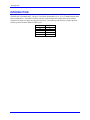
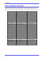
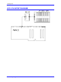
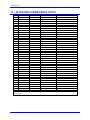
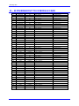
^1 USER MANUAL
^2 Accessory 21A
^3 PMAC2 JOPTO Part Interface for OPTO 22
^4 3Ax-603375-xUxx
^5 October 15, 2003
Single Source Machine Control
Power // Flexibility // Ease of Use
21314 Lassen Street Chatsworth, CA 91311 // Tel. (818) 998-2095 Fax. (818) 998-7807 // www.deltatau.com
Copyright Information
© 2003 Delta Tau Data Systems, Inc. All rights reserved.
This document is furnished for the customers of Delta Tau Data Systems, Inc. Other uses are
unauthorized without written permission of Delta Tau Data Systems, Inc. Information contained
in this manual may be updated from time-to-time due to product improvements, etc., and may not
conform in every respect to former issues.
To report errors or inconsistencies, call or email:
Delta Tau Data Systems, Inc. Technical Support
Phone: (818) 717-5656
Fax: (818) 998-7807
Email: [email protected]
Website: http://www.deltatau.com
Operating Conditions
All Delta Tau Data Systems, Inc. motion controller products, accessories, and amplifiers contain
static sensitive components that can be damaged by incorrect handling. When installing or
handling Delta Tau Data Systems, Inc. products, avoid contact with highly insulated materials.
Only qualified personnel should be allowed to handle this equipment.
In the case of industrial applications, we expect our products to be protected from hazardous or
conductive materials and/or environments that could cause harm to the controller by damaging
components or causing electrical shorts. When our products are used in an industrial
environment, install them into an industrial electrical cabinet or industrial PC to protect them
from excessive or corrosive moisture, abnormal ambient temperatures, and conductive materials.
If Delta Tau Data Systems, Inc. products are directly exposed to hazardous or conductive
materials and/or environments, we cannot guarantee their operation.
Accessory 21A
Table of Contents
INTRODUCTION .......................................................................................................................................................... 1
USING THE PMAC2 JOPTO PORT........................................................................................................................... 3
DIRECTION CONTROL .............................................................................................................................................. 5
INVERSION CONTROL .............................................................................................................................................. 7
ALTERNATE USES ...................................................................................................................................................... 9
EXAMPLE SETUP ...................................................................................................................................................... 11
ACC-21A SETUP DIAGRAM..................................................................................................................................... 15
J1 – 40 PIN INPUT FROM PMAC2 JOPTO............................................................................................................. 17
J2 – 50 PIN BREAKOUT TO I/O MODULE CARD................................................................................................ 19
Table of Contents
i
Accessory 21A
ii
Table of Contents
Accessory 21A
INTRODUCTION
The ACC-21A was created to give the user the capability to use PMAC2’s JOPTO port with OPTO 22 or
Grayhill style I/O module racks. The ACC-21A can be used with the 8, 16, 24, or 32 module boards from
these manufacturers. The PMAC2 JOPTO port has 32 bits of inputs and outputs that can be software
configured as inputs or outputs on a byte-by-byte basis. The following table lists the possible input/out
schemes possible with the PMAC2 JOPTO port.
Introduction
Inputs
Outputs
32
24
16
8
0
0
8
16
24
32
1
Accessory 21A
2
Introduction
Accessory 21A
USING THE PMAC2 JOPTO PORT
The 32 I/O lines are memory-mapped into PMAC's address space in registers Y:$C080 and Y:$C081 for
PMAC2 and Y:$78400 and Y:$78401 for Turbo PMAC2. Typically these I/O lines are accessed
individually with M-variables. Following is a suggested set of M-variable definitions to use these data
lines:
PMAC2
Turbo PMAC2
Description
M0->Y:$C080,0
M1->Y:$C080,1
M2->Y:$C080,2
M3->Y:$C080,3
M4->Y:$C080,4
M5->Y:$C080,5
M6->Y:$C080,6
M7->Y:$C080,7
M8->Y:$C080,8
M9->Y:$C080,9
M10->Y:$C080,10
M11->Y:$C080,11
M12->Y:$C080,12
M13->Y:$C080,13
M14->Y:$C080,14
M15->Y:$C080,15
M16->Y:$C080,16
M17->Y:$C080,17
M18->Y:$C080,18
M19->Y:$C080,19
M20->Y:$C080,20
M21->Y:$C080,21
M22->Y:$C080,22
M23->Y:$C080,23
M24->Y:$C081,0
M25->Y:$C081,1
M26->Y:$C081,2
M27->Y:$C081,3
M28->Y:$C081,4
M29->Y:$C081,5
M30->Y:$C081,6
M31->Y:$C081,7
M0->Y:$78400,0
M1->Y:$78400,1
M2->Y:$78400,2
M3->Y:$78400,3
M4->Y:$78400,4
M5->Y:$78400,5
M6->Y:$78400,6
M7->Y:$78400,7
M8->Y:$78400,8
M9->Y:$78400,9
M10->Y:$78400,10
M11->Y:$78400,11
M12->Y:$78400,12
M13->Y:$78400,13
M14->Y:$78400,14
M15->Y:$78400,15
M16->Y:$78400,16
M17->Y:$78400,17
M18->Y:$78400,18
M19->Y:$78400,19
M20->Y:$78400,20
M21->Y:$78400,21
M22->Y:$78400,22
M23->Y:$78400,23
M24->Y:$78401,0
M25->Y:$78401,1
M26->Y:$78401,2
M27->Y:$78401,3
M28->Y:$78401,4
M29->Y:$78401,5
M30->Y:$78401,6
M31->Y:$78401,7
I/O00 Data Line J3 Pin 1
I/O01 Data Line J3 Pin 2
I/O02 Data Line J3 Pin 3
I/O03 Data Line J3 Pin 4
I/O04 Data Line J3 Pin 5
I/O05 Data Line J3 Pin 6
I/O06 Data Line J3 Pin 7
I/O07 Data Line J3 Pin 8
I/O08 Data Line J3 Pin 9
I/O09 Data Line J3 Pin 10
I/O10 Data Line J3 Pin 11
I/O11 Data Line J3 Pin 12
I/O12 Data Line J3 Pin 13
I/O13 Data Line J3 Pin 14
I/O14 Data Line J3 Pin 15
I/O15 Data Line J3 Pin 16
I/O16 Data Line J3 Pin 17
I/O17 Data Line J3 Pin 18
I/O18 Data Line J3 Pin 19
I/O19 Data Line J3 Pin 20
I/O20 Data Line J3 Pin 21
I/O21 Data Line J3 Pin 22
I/O22 Data Line J3 Pin 23
I/O23 Data Line J3 Pin 24
I/O24 Data Line J3 Pin 25
I/O25 Data Line J3 Pin 26
I/O26 Data Line J3 Pin 27
I/O27 Data Line J3 Pin 28
I/O28 Data Line J3 Pin 29
I/O29 Data Line J3 Pin 30
I/O30 Data Line J3 Pin 31
I/O31 Data Line J3 Pin 32
Using the PMAC2 JOPTO Port
3
Accessory 21A
4
Using the PMAC2 JOPTO Port
Accessory 21A
DIRECTION CONTROL
The PMAC2 JIO direction control is used to setup the I/O bytes as either inputs or outputs. The direction
control bit for each of these I/O bits is in the corresponding bit in the matching X register. For example,
the direction control bit for I/O03 is located at X:$C080,3 and X:$78400,3 for Turbo PMAC2; the
direction control bit for I/O30 is located at X:$C081,6 and X:$78401,6 for Turbo PMAC2. Because the
buffer ICs can only be switched by byte, it is best to define 8-bit M-variables for the direction control.
Suggested definitions are:
PMAC2
Turbo PMAC2
Description
M32->X:$C080,0,8
M34->X:$C080,8,8
M36->X:$C080,16,8
M38->X:$C081,0,8
M32->X:$78400,0,8
M34->X:$78400,8,8
M36->X:$78400,16,8
M38->X:$78401,0,8
Direction control for I/O00 to I/O07
Direction control for I/O08 to I/O15
Direction control for I/O16 to I/O23
Direction control for I/O24 to I/O31
These M-variables should take values of 0 or 255 ($FF) only; 0 sets the byte to input, 255 sets the byte to
output.
In addition, the bi-directional buffer IC for each byte has a direction control line accessible as a software
control bit. These control lines and bits must match the ASIC direction bits. The buffer direction control
bits are at PMAC address Y:$E800 or Y:$70800, with bits 0 to 3 controlling the four bytes of the JIO
port. A bit value of 0 specifies input; 1 specifies output. Suggested M-variable definitions are:
PMAC2
Turbo PMAC2
Description
M33->Y:$E800,0
M35->Y:$E800,1
M37->Y:$E800,2
M39->Y:$E800,3
M33->Y:$70800,0
M35->Y:$70800,1
M37->Y:$70800,2
M39->Y:$70800,3
Buffer direction control for I/O00 to I/O07
Buffer direction control for I/O08 to I/O15
Buffer direction control for I/O16 to I/O23
Buffer direction control for I/O24 to I/O31
In the default configuration automatically set at power-up/reset, I/O00 to I/O31 are set up as inputs (M882
through M889 = 0). This is done for maximum safety; no lines can be forced into an undesirable high or
low state. Any of these lines that are to be used as outputs must be changed to outputs by user programs
(usually this is done in PLC 1 acting as a "reset" PLC, scanning through once on power-up/reset, then
disabling itself).
Direction Control
5
Accessory 21A
6
Direction Control
Accessory 21A
INVERSION CONTROL
Each line on the JIO port is individually controllable as to whether it is an inverting I/O point (0=+5V;
1=0V) or a non-inverting I/O point (0=0V; 1=+5V).
PMAC2
M80->X:$C084,0,24
M81->X:$C085,0,8
Turbo PMAC2
M80->X:$78404,0,24
M81->X:$78405,0,8
Description
Inversion control for bits 0 to 23
Inversion control for bits 24 to 31
A value of 0 in the control bit sets the corresponding I/O point as non-inverting. A value of 1 in the
control bits sets the corresponding I/O point as inverting. At power-up/reset, PMAC automatically sets
all of the I/O points on the JIO port as non-inverting.
Inversion Control
7
Accessory 21A
8
Inversion Control
Accessory 21A
ALTERNATE USES
Each general-purpose I/O point on the JIO port has an alternate use as a supplemental fixed-use I/O point
on a supplemental machine interface channel (1* or 2*). The points are individually controllable as to
general-purpose use or fixed use by control registers Y:$C084 and Y:$C085. Refer to these registers in
the memory-I/O map to see the alternate uses of each point. At power-up/reset, PMAC2 automatically
sets up all of the I/O points on the port for general-purpose use.
Note:
The direction-control of the buffer ICs must be set properly for the alternate uses
of the I/O points, just as for the general-purpose I/O uses.
Alternate Uses`
9
Accessory 21A
10
Alternate Uses
Accessory 21A
EXAMPLE SETUP
For this example we will setup the first 2 bytes of the JIO port as outputs and the last two bytes will be
setup as inputs. We also would like the logic for all inputs and outputs to be non-inverting (0=0V;
1=+5V).
#define
JIO_OUT_0
M0
#define
#define
#define
#define
#define
#define
#define
#define
#define
#define
#define
#define
#define
#define
#define
#define
#define
#define
#define
#define
#define
#define
#define
#define
#define
#define
#define
#define
#define
#define
#define
#define
#define
#define
#define
#define
#define
#define
#define
#define
#define
JIO_OUT_1
JIO_OUT_2
JIO_OUT_3
JIO_OUT_4
JIO_OUT_5
JIO_OUT_6
JIO_OUT_7
JIO_OUT_8
JIO_OUT_9
JIO_OUT_10
JIO_OUT_11
JIO_OUT_12
JIO_OUT_13
JIO_OUT_14
JIO_OUT_15
JIO_IN_0
JIO_IN_1
JIO_IN_2
JIO_IN_3
JIO_IN_4
JIO_IN_5
JIO_IN_6
JIO_IN_7
JIO_IN_8
JIO_IN_9
JIO_IN_10
JIO_IN_11
JIO_IN_12
JIO_IN_13
JIO_IN_14
JIO_IN_15
DIR_CONTROL_1
BUF_CONTROL_1
DIR_CONTROL_2
BUF_CONTROL_2
DIR_CONTROL_3
BUF_CONTROL_3
DIR_CONTROL_4
BUF_CONTROL_4
INV_CTRL_0_23
INV_CTRL_24_31
M1
M2
M3
M4
M5
M6
M7
M8
M9
M10
M11
M12
M13
M14
M15
M16
M17
M18
M19
M20
M21
M22
M23
M24
M25
M26
M27
M28
M29
M30
M31
M32
M33
M34
M35
M36
M37
M38
M39
M80
M81
M0->Y:$C080,0
M1->Y:$C080,1
M2->Y:$C080,2
M3->Y:$C080,3
M4->Y:$C080,4
Example Setup
;
;
;
;
;
I/O00
I/O01
I/O02
I/O03
I/O04
Data
Data
Data
Data
Data
Line;
Line;
Line;
Line;
Line;
J3
J3
J3
J3
J3
Pin
Pin
Pin
Pin
Pin
1
2
3
4
5
11
Accessory 21A
M5->Y:$C080,5
M6->Y:$C080,6
M7->Y:$C080,7
M8->Y:$C080,8
M9->Y:$C080,9
M10->Y:$C080,10
M11->Y:$C080,11
M12->Y:$C080,12
M13->Y:$C080,13
M14->Y:$C080,14
M15->Y:$C080,15
M16->Y:$C080,16
M17->Y:$C080,17
M18->Y:$C080,18
M19->Y:$C080,19
M20->Y:$C080,20
M21->Y:$C080,21
M22->Y:$C080,22
M23->Y:$C080,23
M24->Y:$C081,0
M25->Y:$C081,1
M26->Y:$C081,2
M27->Y:$C081,3
M28->Y:$C081,4
M29->Y:$C081,5
M30->Y:$C081,6
M31->Y:$C081,7
M32->X:$C080,0,8
M34->X:$C080,8,8
M36->X:$C080,16,8
M38->X:$C081,0,8
M33->Y:$E800,0
M35->Y:$E800,1
M37->Y:$E800,2
M39->Y:$E800,3
M80->X:$C084,0,24
M81->X:$C085,0,8
;
;
;
;
;
;
;
;
;
;
;
;
;
;
;
;
;
;
;
;
;
;
;
;
;
;
;
;
;
;
;
;
;
;
;
;
;
I/O05 Data Line; J3 Pin 6
I/O06 Data Line; J3 Pin 7
I/O07 Data Line; J3 Pin 8
I/O08 Data Line; J3 Pin 9
I/O09 Data Line; J3 Pin 10
I/O10 Data Line; J3 Pin 11
I/O11 Data Line; J3 Pin 12
I/O12 Data Line; J3 Pin 13
I/O13 Data Line; J3 Pin 14
I/O14 Data Line; J3 Pin 15
I/O15 Data Line; J3 Pin 16
I/O16 Data Line; J3 Pin 17
I/O17 Data Line; J3 Pin 18
I/O18 Data Line; J3 Pin 19
I/O19 Data Line; J3 Pin 20
I/O20 Data Line; J3 Pin 21
I/O21 Data Line; J3 Pin 22
I/O22 Data Line; J3 Pin 23
I/O23 Data Line; J3 Pin 24
I/O24 Data Line; J3 Pin 25
I/O25 Data Line; J3 Pin 26
I/O26 Data Line; J3 Pin 27
I/O27 Data Line; J3 Pin 28
I/O28 Data Line; J3 Pin 29
I/O29 Data Line; J3 Pin 30
I/O30 Data Line; J3 Pin 31
I/O31 Data Line; J3 Pin 32
Direction control for I/O00 to I/O07
Direction control for I/O08 to I/O15
Direction control for I/O16 to I/O23
Direction control for I/O24 to I/O31
Buffer direction control for I/O00 to
Buffer direction control for I/O08 to
Buffer direction control for I/O16 to
Buffer direction control for I/O24 to
Inversion control for bits 0 to 23
Inversion control for bits 24 to 31
I/O07
I/O15
I/O23
I/O31
If the above definitions were made, we could set these variables to their proper values in an initialization
PLC. I usually will use the following technique for an initialization PLC,
OPEN PLC 6 CLEAR
DIR_CONTROL_1 = 255
BUF_CONTROL_1 = 1
DIR_CONTROL_2 = 255
BUF_CONTROL_2 = 1
DIR_CONTROL_3 = 0
BUF_CONTROL_3 = 0
DIR_CONTROL_4 = 0
BUF_CONTROL_4 = 0
INV_CTRL_0_23 = 0
INV_CTRL_24_31 =0
12
;set
;set
;set
;set
;set
;set
;set
;set
;set
;set
as
as
as
as
as
as
as
as
as
as
output
output
output
output
input
input
input
input
non-inverting
non-inverting
Example Setup
Accessory 21A
;place other initialization variables here
while (1<2)
.
.
;PLC in here (perhaps E_STOP routine)
.
.
endwhile
CLOSE
Using this technique, we will have a one-time read of the initialization variables used by the card and the
logic for the PLCs.
Example Setup
13
Accessory 21A
14
Example Setup
Accessory 21A
ACC-21A SETUP DIAGRAM
Acc-21A Setup Diagram
15
Accessory 21A
16
Acc-21A Setup Diagram
Accessory 21A
J1 – 40 PIN INPUT FROM PMAC2 JOPTO
Pin #
Symbol
Function
Description
Notes
1
I/O00
I/O
Digital I/O 0
Software Direction Control
2
I/O01
I/O
Digital I/O 1
Software Direction Control
3
I/O02
I/O
Digital I/O 2
Software Direction Control
4
I/O03
I/O
Digital I/O 3
Software Direction Control
5
I/O04
I/O
Digital I/O 4
Software Direction Control
6
I/O05
I/O
Digital I/O 5
Software Direction Control
7
I/O06
I/O
Digital I/O 6
Software Direction Control
8
I/O07
I/O
Digital I/O 7
Software Direction Control
9
I/O08
I/O
Digital I/O 8
Software Direction Control
10
I/O09
I/O
Digital I/O 9
Software Direction Control
11
I/O10
I/O
Digital I/O 10
Software Direction Control
12
I/O11
I/O
Digital I/O 11
Software Direction Control
13
I/O12
I/O
Digital I/O 12
Software Direction Control
14
I/O13
I/O
Digital I/O 13
Software Direction Control
15
I/O14
I/O
Digital I/O 14
Software Direction Control
16
I/O15
I/O
Digital I/O 15
Software Direction Control
17
I/O16
I/O
Digital I/O 16
Software Direction Control
18
I/O17
I/O
Digital I/O 17
Software Direction Control
19
I/O18
I/O
Digital I/O 18
Software Direction Control
20
I/O19
I/O
Digital I/O 19
Software Direction Control
21
I/O20
I/O
Digital I/O 20
Software Direction Control
22
I/O21
I/O
Digital I/O 21
Software Direction Control
23
I/O22
I/O
Digital I/O 22
Software Direction Control
24
I/O23
I/O
Digital I/O 23
Software Direction Control
25
I/O24
I/O
Digital I/O 24
Software Direction Control
26
I/O25
I/O
Digital I/O 25
Software Direction Control
27
I/O26
I/O
Digital I/O 26
Software Direction Control
28
I/O27
I/O
Digital I/O 27
Software Direction Control
29
I/O28
I/O
Digital I/O 28
Software Direction Control
30
I/O29
I/O
Digital I/O 29
Software Direction Control
31
I/O30
I/O
Digital I/O 30
Software Direction Control
32
I/O31
I/O
Digital I/O 31
Software Direction Control
33
GND
Common
Ref. Voltage
34
GND
Common
Ref. Voltage
35
PHASE/
Output
Phase Clock
For latching data
36
SERVO/
Output
Servo Clock
For latching data
37
GND
Common
Ref. Voltage
38
GND
Common
Ref. Voltage
39
+5V
Output
Supply Digital Voltage
To power ext. circuitry
40
+5V
Output
Supply Voltage
To power ext. circuitry
The JI/O connector provides 32 input/output pins at TTL levels. Direction can be controlled in bytewide groups.
J1 – 40 Pin Input from PMAC2 JOPTO
17
Accessory 21A
18
J1 – 40 Pin Input from PMAC2 JOPTO
Accessory 21A
J2 – 50 PIN BREAKOUT TO I/O MODULE CARD
Pin #
Symbol
Function
1
2
3
4
5
6
7
8
9
10
11
12
13
14
15
16
17
18
19
20
21
22
23
24
25
26
27
28
29
30
31
32
33
34
35
36
37
38
39
40
41
42
43
44
45
46
47
48
49
50
IN/OUT23
IN/OUT24
IN/OUT22
IN/OUT25
IN/OUT21
IN/OUT26
IN/OUT20
IN/OUT27
IN/OUT19
IN/OUT28
IN/OUT18
IN/OUT29
IN/OUT17
IN/OUT30
IN/OUT16
IN/OUT31
IN/OUT15
GND
IN/OUT14
GND
IN/OUT13
GND
IN/OUT12
GND
IN/OUT11
GND
IN/OUT10
GND
IN/OUT9
GND
IN/OUT8
GND
IN/OUT7
GND
IN/OUT6
GND
IN/OUT5
GND
IN/OUT4
GND
IN/OUT3
GND
IN/OUT2
GND
IN/OUT1
GND
IN/OUT0
GND
A +5V
GND
I/O
I/O
I/O
I/O
I/O
I/O
I/O
I/O
I/O
I/O
I/O
I/O
I/O
I/O
I/O
I/O
I/O
Common
I/O
Common
I/O
Common
I/O
Common
I/O
Common
I/O
Common
I/O
Common
I/O
Common
I/O
Common
I/O
Common
I/O
Common
I/O
Common
I/O
Common
I/O
Common
I/O
Common
I/O
Common
Output
Common
J2 – 50 Pin Breakout to I/O Module Card
Description
Port A Bit 23
Port A Bit 24
Port A Bit 22
Port A Bit 25
Port A Bit 21
Port A Bit 26
Port A Bit 20
Port A Bit 27
Port A Bit 19
Port A Bit 28
Port A Bit 18
Port A Bit 29
Port A Bit 17
Port A Bit 30
Port A Bit 16
Port A Bit 31
Port A Bit 15
Opto Common
Port A Bit 14
Opto Common
Port A Bit 13
Opto Common
Port A Bit 12
Opto Common
Port A Bit 11
Opto Common
Port A Bit 10
Opto Common
Port A Bit 9
Opto Common
Port A Bit 8
Opto Common
Port A Bit 7
Opto Common
Port A Bit 6
Opto Common
Port A Bit 5
Opto Common
Port A Bit 4
Opto Common
Port A Bit 3
Opto Common
Port A Bit 2
Opto Common
Port A Bit 1
Opto Common
Port A Bit 0
Opto Common
+5 V supply
Opto Common
Notes
User Defined I/O
User Defined I/O
User Defined I/O
User Defined I/O
User Defined I/O
User Defined I/O
User Defined I/O
User Defined I/O
User Defined I/O
User Defined I/O
User Defined I/O
User Defined I/O
User Defined I/O
User Defined I/O
User Defined I/O
User Defined I/O
User Defined I/O
User Defined I/O
User Defined I/O
User Defined I/O
User Defined I/O
User Defined I/O
User Defined I/O
User Defined I/O
User Defined I/O
User Defined I/O
User Defined I/O
User Defined I/O
User Defined I/O
User Defined I/O
User Defined I/O
User Defined I/O
19
Accessory 21A
20
J2 – 50 Pin Breakout to I/O Module Card