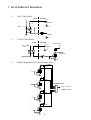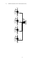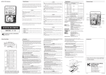
1
DIO-3232
DIGITAL I/O CARD
USER’S MANUAL (V1.2)
健昇科技股份有限公司
JS AUTOMATION CORP.
台北縣汐止市㆗興路 100 號 6 樓
6F,NO.100,CHUNG-SHIN RD.
SHI-TSU,TAIPEI,TAIWAN,R.O.C.
TEL:886-2-2647-6936
FAX:886-2-2647-6940
http://www.automation.com.tw
E-mail:[email protected]
[email protected]
Export: [email protected]
Contents
1. FORWARD ............................................................
............................................................ 2
2. PACKING LIST .......................................................
....................................................... 2
3. FEATURES ............................................................
............................................................ 3
4. SPECIFICATIONS ....................................................
.................................................... 4
4.1
4.2
DIO-3232 MAIN CARD...................................................................................................... 4
DIO-3232 DIN RAIL MOUNTED WIRING BOARD ....................................................... 4
5. LAYOUT
5.1
5.2
5.3
..............................................................
.............................................................. 5
DIO-3232 MAIN CARD LAYOUT..................................................................................... 5
DIO-3232 WIRING BOARD LAYOUT (N MOS) ............................................................. 5
DIO-3232 WIRING BOARD LAYOUT (P MOS).............................................................. 6
6. PIN DEFINITIONS ...................................................
................................................... 7
6.1
6.2
FRONT VIEW OF CONNECTOR .................................................................................... 7
PIN DEFINITIONS.............................................................................................................. 7
7. I/O INTERFACE DIAGRAM
7.1
7.2
7.3
7.4
........................................
........................................ 8
INPUT DIAGRAM ............................................................................................................ 8
OUTPUT DIAGRAM ........................................................................................................ 8
WIRING BOARD OUTPUT DIAGRAM(N MOS)............................................................ 8
WIRING BOARD OUTPUT DIAGRAM(P MOS)............................................................. 9
8. EXTERNAL WIRING DIAGRAM ..................................
.................................. 10
8.1
8.2
EXTERNAL WIRING DIAGRAM (N MOS)................................................................... 10
EXTERNAL WIRING DIAGRAM(P MOS) .................................................................... 11
9. HARDWARE SETTINGS
9.1
...........................................
........................................... 12
CARD ID SETTING ............................................................................................................... 12
10. APPLICATIONS .....................................................
..................................................... 13
11. APPLICATION NOTE...............................................
............................................... 14
11.1
TIP FOR USING NPN TYPE PROXIMITY S/W: ..................................................................... 14
11.2
TIP FOR USING PNP TYPE PROXIMITY S/W:...................................................................... 14
12. DIMENSIONS ........................................................
........................................................ 15
12.1 DIO-3232 MAIN CARD DIMENSION ............................................................................ 15
12.2 DIO-3232 WIRING BOARD DIMENSION ..................................................................... 15
13. ORDER INFORMATION
...........................................
........................................... 16
1
1. FORWARD
Thank you for your selection of JAC’s product DIO-3232 32 inputs and 32 outputs DIGITAL I/O
card for IBM compatible industrial PC. In the field of industrial control, digital I/O is generally
controlled under a microprocessor and owing to their specific consideration of industrial
environment, it is quite different from the laboratory requirement.
This card is a FPGA based design and our experience in the noise immunity makes this card very
stable in the noisy environment and you don’t worry about computer down by external noise. we
wish the card that will be helpful to your project.
Other DIO series products:
DIO-9201Æ16IN+16OUT digital I/O card
DIO-2232Æ32IN+32OUT digital I/O card (ISA bus)
DIO-2248Æ48IN+16OUT digital I/O card (ISA bus)
DIO-2264Æ64IN digital Input card (ISA bus)
DIO-3248Æ48IN+16OUT digital I/O card (PCI bus)
DIO-3264Æ64IN digital Input card (PCI bus)
Any comment is welcome,
please visit our website: www.automation.com.tw for the up to date information.
2. PACKING LIST
2.1
2.2
2.3
DIO-3232 main card
DIO-3232 DIN rail mounted wiring board
SCSIⅡ68 PINCABLE(1.5m)
1
1
1
2.4
2.5
Accessories
DEMO CD
1
1
2
3. FEATURES
3.1
3.2
3.3
3.4
3.5
3.6
PCI plug and play function with card ID for 16 identical cards
All of inputs and outputs are photo-coupler isolated
Build-in input de-bounce circuit
LEDs for corresponding status indication
8 digits per I/O group with Green LED at first digit
Power MOS type output for high speed DC load
3
4. SPECIFICATIONS
4.1
4.2
DIO-3232 MAIN CARD
4.1.1
Input photo-coupler isolation voltage ― 2500Vac 1Min
4.1.2
Insulation resistance ― 100M Ohm (min) at 1000Vdc
4.1.3
PCI bus data width ― 32 bits
4.1.4
Card ID ― 4 bits
4.1.5
Switching speed ― 2.2KHZ max. ( with on board debounce circuit)
4.1.6
Input “ON” state ― 2.8V(max) 4.5ma(min)
4.1.7
Input “OFF” state ― 8V(min) 3ma(max)
4.1.8
Output channel ― 32 ea of ON/OFF switching
4.1.9
I/O connector ― 68 pin female mini scsi connector
4.1.10
Wiring board ― 1 with round cable hook to main card
4.1.11
External supply ― DC 24± 4V
4.1.12
Operation temperature ― 0 to 70° C
4.1.13
Operation humidity ― RH5~95%, non-condensed
4.1.14
Dimension ― 176(W)*122(H)mm
DIO-3232 DIN RAIL MOUNTED WIRING BOARD
4.2.1
4.2.2
External supply ―DC 24V± 4V
Input status indicator ― 32 LED, 8 digit per group with Green LED at first
4.2.3
digit
Output status indicator ― 32 LED, 8 digit per group with Green LED at first
4.2.4
4.2.5
digit
Power indicator ― Red LED
Terminal ― every 4 has one common terminal.
4.2.6
4.2.7
4.2.8
4.2.9
(Different “common” for different positive power terminal )
Output capacity ―POWER MOS output, 1A continuous、120V DC (N MOS
max) 、24V DC (P MOS max)
Operation temperature ― 0 to 70° C
Operation humidity ― RH5~95%, non-condensed
Dimension ― 155(W)*107(H)mm
4
5. LAYOUT
5.1
DIO-3232 MAIN CARD LAYOUT
CARD ID
DIP SWITCH
5.2
DIO-3232 WIRING BOARD LAYOUT (N MOS)
5
5.3
DIO-3232 WIRING BOARD LAYOUT (P MOS)
6
6. PIN DEFINITIONS
6.1
6.2
PIN
1
2
3
4
5
6
7
8
9
10
11
12
13
14
15
16
17
18
19
20
21
22
23
24
25
26
27
28
29
30
31
32
33
34
FRONT VIEW OF CONNECTOR
PIN DEFINITIONS
Descriptions
EXT_IN0 [ External Input 0 ]
EXT_IN2 [ External Input 2 ]
EXT_IN4 [ External Input 4 ]
EXT_IN6 [ External Input 6 ]
EXT_IN8 [ External Input 8 ]
EXT_IN10 [ External Input 10 ]
EXT_IN12 [ External Input 12 ]
EXT_IN14 [ External Input 14 ]
EXT_IN16 [ External Input 16 ]
EXT_IN18 [ External Input 18 ]
EXT_IN20 [ External Input 20 ]
EXT_IN22 [ External Input 22 ]
EXT_IN24 [ External Input 24 ]
EXT_IN26 [ External Input 26 ]
EXT_IN28 [ External Input 28 ]
EXT_IN30 [ External Input 30 ]
EXT_OUT0 [ External Output 0 ]
EXT_OUT2 [ External Output 2 ]
EXT_OUT4 [ External Output 4 ]
EXT_OUT6 [ External Output 6 ]
EXT_OUT8 [ External Output 8 ]
EXT_OUT10 [ External Output 10 ]
EXT_OUT12 [ External Output 12 ]
EXT_OUT14 [ External Output 14 ]
EXT_OUT16 [ External Output 16 ]
EXT_OUT18 [ External Output 18 ]
EXT_OUT20 [ External Output 20 ]
EXT_OUT22 [ External Output 22 ]
EXT_OUT24 [ External Output 24 ]
EXT_OUT26 [ External Output 26 ]
EXT_OUT28 [ External Output 28 ]
EXT_OUT30 [ External Output 30 ]
+24V [ External DC24V power ]
+24V [ External DC24V power ]
PIN
35
36
37
38
39
40
41
42
43
44
45
46
47
48
49
50
51
52
53
54
55
56
57
58
59
60
61
62
63
64
65
66
67
68
7
Descriptions
EXT_IN1 [ External Input 1 ]
EXT_IN3 [ External Input 3 ]
EXT_IN5 [ External Input 5 ]
EXT_IN7 [ External Input 7 ]
EXT_IN9 [ External Input 9 ]
EXT_IN11 [ External Input 11 ]
EXT_IN13 [ External Input 13 ]
EXT_IN15 [ External Input 15 ]
EXT_IN17 [ External Input 17 ]
EXT_IN19 [ External Input 19 ]
EXT_IN21 [ External Input 21 ]
EXT_IN23 [ External Input 23 ]
EXT_IN25 [ External Input 25 ]
EXT_IN27 [ External Input 27 ]
EXT_IN29 [ External Input 29 ]
EXT_IN31 [ External Input 31 ]
EXT_OUT1 [ External Output 1 ]
EXT_OUT3 [ External Output 3 ]
EXT_OUT5 [ External Output 5 ]
EXT_OUT7 [ External Output 7 ]
EXT_OUT9 [ External Output 9 ]
EXT_OUT11 [ External Output 11 ]
EXT_OUT13 [ External Output 13 ]
EXT_OUT15 [ External Output 15 ]
EXT_OUT17 [ External Output 17 ]
EXT_OUT19 [ External Output 19 ]
EXT_OUT21 [ External Output 21 ]
EXT_OUT23 [ External Output 23 ]
EXT_OUT25 [ External Output 25 ]
EXT_OUT27 [ External Output 27 ]
EXT_OUT29 [ External Output 29 ]
EXT_OUT31 [ External Output 31 ]
+24V [ External DC24V power ]
+24V [ External DC24V power ]
7. I/O INTERFACE DIAGRAM
7.1
INPUT DIAGRAM
CARD
ADAPTER
+5V
+24Ve
EXT_IN +24V
3.3K
1
4
COM
2
3
330
EXT_IN
COM
7.2
OUTPUT DIAGRAM
CARD
ADAPTER
+24Ve
DC5V~DC120V
+5V
extVn
4
1
EXT_IN +24V
3
2
COM
EXT_OUT
COM
7.3
WIRING BOARD OUTPUT DIAGRAM(N MOS)
COMA
O3
COM
O2
MOSFET OUTPUT
5
4
3
2
1
COM
O1
COM
O0
COM
8
CON
4 outputs with one
common (extV+)
7.4
WIRING BOARD OUTPUT DIAGRAM(P MOS)
+24Ve
R
OUT3
PMOS
DIODE
+24Ve
R
EXTG
OUT2
PMOS
DIODE
+24Ve
R
OUT1
PMOS
DIODE
+24Ve
R
PMOS
OUT0
DIODE
9
5
4
3
2
1
8. EXTERNAL WIRING DIAGRAM
8.1
EXTERNAL WIRING DIAGRAM (N MOS)
OUTPUT EXAMPLE
INPUT EXAMPLE
IN0
O0
Load
IN1
O1
Load
IN2
O2
Load
IN3
O3
Load
COM
extV2
IN4
.
.
.
.
.
.
.
.
.
.
.
.
DIO3232
ADAPTER
MAX 120Vdc
O4
Load
O5
Load
O6
Load
O7
Load
extV2
5Vdc
O8
.
.
.
.
.
O31
IN31
+24V
DC24V
COM
(GND)
※ If different group of output use different voltage source, please make sure to connect the Vtogether to the ground of external DC24V power supply.
10
8.2
EXTERNAL WIRING DIAGRAM(P MOS)
INPUT EXAMPLE
OUTPUT EXAMPLE
IN0
EXTG
IN1
+24Vi
DC
IN2
IN3
EXTG
EXTG
IN4
32I/32O
ADAPTER
IN31
O31
DC
Load
O30
DC
Load
O29
DC
Load
O28
DC
Load
+24Vdc Load
O27
O0
11
9. HARDWARE SETTINGS
9.1
Card ID setting
Since PCI cards have plug and play function, the card ID is required for programmer
to identify which card he/she will control without knowing the physical address
assigned by the Windows. A 4 bits DIP switch for distinguishing the 16 identical card.
The following example sets the card ID at 12.
DIP SW SETTING:
:(ID=12)
8
4
2
1
1
2
3
4
Weighting
ON
0
1
12
10. APPLICATIONS
10.1
10.2
Accept:- P.B./M.S./EMG./Contact- Start/Stop/Limit swith/sensor
- Interlock/selective Sw.- Proximity switch
- Aux. contact of transducer/detector
As I/O of S/W PLC Controller
Power MOS type output: drive high speed DC load
13
11. APPLICATION NOTE
11.1
Tip for using NPN type proximity S/W:
The NPN type proximity sensor can directly connect to input of wring board.
+24V
NPN
OUTPUT
INPUT
GND
Wring board
+24V
+24V
3.3K
1
4
2
3
330
O/P
I/P
GND
GND
11.2 Tip for using PNP type proximity S/W:
The PNP type proximity sensor need extra pull down resister connect to input of wring
board.
+24V
PNP
OUTPUT
INPUT
1.5K
1/2W
GND
Wring board
+24V
+24V
3.3K
330
I/P
O/P
1.5K
1/2W
GND
14
GND
1
4
2
3
12. DIMENSIONS
12.1
DIO-3232 MAIN CARD DIMENSION
12.2
DIO-3232 WIRING BOARD DIMENSION
15
13. ORDER INFORMATION
PRODUCT
DIO-3232
DIO-3232 DMO
DIO-3232 WIN
DIO-3232 LBV
DIO-3232 DIN
DESCRIPTIONS
Main card: 32 In and 32 Out with photo-coupler isolated
Demo program of DIO-3232 card for DOS (free with user manual)
Dll (VB/VC/C++ Builder) of DIO-3232 card for Win95/98/NT
Vi of DIO-3232 card for LabVIEW i
DIN rail mounted wiring board for 32 input and 32 output
16