1
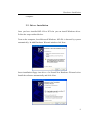
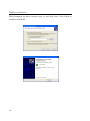
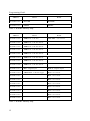
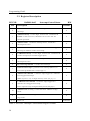
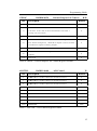
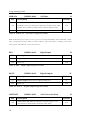
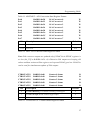
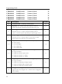
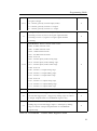
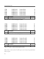
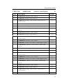
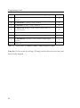
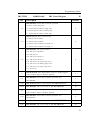
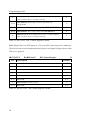
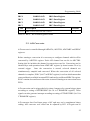
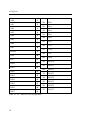
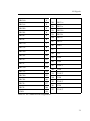
MF 624
M ULTIFUNCTION I/O CARD
USER'S MANUAL
© 2014
HUMUSOFT ®
© C O PY R IG H T 2014 by H U M U SO FT s.r.o.. A ll rights reserved.
N o part of this publication m ay be reproduced or distributed in any form or by any means, or
stored in a database or retrieval system, w ithout the prior w ritten consent of H U M U SO FT
s.r.o.
L im ited W arranty: H U M U SO FT s.r.o. disclaims all liability for any direct or indirect
damages caused by use or misuse of the M F 624 device or this documentation.
H U M U SO FT is a registered trademark of H U M U SO FT s.r.o.
O ther brand and product names are trademarks or registered trademarks of their respective
holders.
Printed in Czech Republic
Table of Contents
Table of Contents
1. Introduction
4
1.1. General Description . . . . . . . . . . . . . . . . . . . . . . . . . . . . . . . . . . . . . . . 4
1.2. Features List . . . . . . . . . . . . . . . . . . . . . . . . . . . . . . . . . . . . . . . . . . . . . 4
1.3. Specifications . . . . . . . . . . . . . . . . . . . . . . . . . . . . . . . . . . . . . . . . . . . . 5
1.3.1. A/D Converter . . . . . . . . . . . . . . . . . . . . . . . . . . . . . . . . . . . . . . . 5
1.3.2. D/A Converter . . . . . . . . . . . . . . . . . . . . . . . . . . . . . . . . . . . . . . . 6
1.3.3. Digital Inputs . . . . . . . . . . . . . . . . . . . . . . . . . . . . . . . . . . . . . . . . 6
1.3.4. Digital Outputs . . . . . . . . . . . . . . . . . . . . . . . . . . . . . . . . . . . . . . 6
1.3.5. Quadrature Encoder Inputs . . . . . . . . . . . . . . . . . . . . . . . . . . . . . 6
1.3.6. Counters/Timers . . . . . . . . . . . . . . . . . . . . . . . . . . . . . . . . . . . . . 7
2. Installation
8
2.1. Board Installation . . . . . . . . . . . . . . . . . . . . . . . . . . . . . . . . . . . . . . . . . 8
2.2. Driver Installation . . . . . . . . . . . . . . . . . . . . . . . . . . . . . . . . . . . . . . . . . 9
3. Programming Guide
11
3.1. Register Map . . . . . . . . . . . . . . . . . . . . . . . . . . . . . . . . . . . . . . . . . . . 11
3.2. Register Description . . . . . . . . . . . . . . . . . . . . . . . . . . . . . . . . . . . . . . 14
3.3. A/D Converter . . . . . . . . . . . . . . . . . . . . . . . . . . . . . . . . . . . . . . . . . . 25
3.4. D/A Converters . . . . . . . . . . . . . . . . . . . . . . . . . . . . . . . . . . . . . . . . . . 26
3.5. Digital I/O . . . . . . . . . . . . . . . . . . . . . . . . . . . . . . . . . . . . . . . . . . . . . 27
3.6. Quadrature Encoder Inputs . . . . . . . . . . . . . . . . . . . . . . . . . . . . . . . . . 27
3.7. Timer/Counter . . . . . . . . . . . . . . . . . . . . . . . . . . . . . . . . . . . . . . . . . . 28
4. I/O Signals
29
4.1. Output Connector Signal Description . . . . . . . . . . . . . . . . . . . . . . . . . 29
3
Introduction
Introduction
1. Introduction
1.1. General Description
The MF 624 multifunction I/O card is designed for the need of connecting PC
compatible computers to real world signals. The MF 624 contains 8 channel fast
14 bit A/D converter with simultaneous sample/hold circuit, 8 independent 14 bit
D/A converters, 8 bit digital input port and 8 bit digital output port, 4 quadrature
encoder inputs with single-ended or differential interface and 5 timers/counters.
The card is designed for standard data acquisition and control applications and
optimized for use with Real Time Toolbox for Simulink®. MF 624 features fully
32 bit architecture for fast throughput.
1.2. Features List
The MF 624 offers following features:
C
32-bit architecture
C
14 bit A/D converter with simultaneous sample & hold circuit
C
Conversion time 1.6 ìs for single channel or 3.7 ìs for 8 channels
C
8 channel single ended fault protected input multiplexer
C
Input range ±10V
C
Internal clock & voltage reference
C
8 D/A converters with 14 bit resolution and ±10V output range
C
4 quadrature encoder inputs with single-ended or differential interface
4
Introduction
C
Software selectable digital input noise filter (0.3 ìs)
C
Quadrature input frequency up to 2.5 MHz
C
Software selectable index pulse operation
C
4 channel 32-bit timer/counter with 20 ns resolution
C
8 bit TTL compatible digital input port
C
8 bit TTL compatible digital output port
C
Interrupt
C
Requires one PCI 2.3 slot and optional second slot for second connector
C
Can be used in 5V or 3.3V slot
C
Power consumption 500 mA@+5V, 150 mA@+12V, 150 mA@-12V
C
Operating temperature 0°C to +70°C
1.3. Specifications
1.3.1. A/D Converter
Resolution:
14 bits
Number of channels:
8 single ended
Sample/hold circuit:
simultaneous sampling of all channels
Conversion time:
1.6 ìs single channel
1.9 ìs 2 channels
2.5 ìs 4 channels
3.7 ìs 8 channels
FIFO:
8 entries/one conversion cycle
Input ranges:
±10V
Input protection:
±18V
Input impedance:
> 1010 Ohm
5
Introduction
1.3.2. D/A Converter
Resolution:
14 bit
Number of channels:
8
Settling time:
max. 31 ìs (full scale swing, 1/2 LSB)
Slew Rate:
10 V/ìs
Output current:
min. ±10 mA
Short circuit current:
±15 mA
DC output impedance:
max. 0.5 Ohm
Load capacitance:
max. 50 pF
Differential nonlinearity:
±1 LSB
1.3.3. Digital Inputs
Number of bits:
8
Input signal levels:
TTL
Logic 0:
0.8 V max.
Logic 1:
2.0 V min.
1.3.4. Digital Outputs
Number of bits:
8
Output signal levels:
TTL
Logic 0:
0.5 V max. @ 24 mA (sink)
Logic 1:
2.0 V min. @ 15 mA (source)
1.3.5. Quadrature Encoder Inputs
Number of axes:
4 independent
Resolution:
32 bits
6
Introduction
Counter modes:
quadrature X4 or up/down counter
Index input:
programmable
Inputs:
differential with Schmitt triggers
Input noise filter:
digital, programmable (0.3 ìs)
Input frequency:
max. 2.5 MHz
1.3.6. Counters/Timers
Counter chip:
custom
Number of channels:
5, 4 of them available on I/O connector, one used
Resolution:
32 bits
Clock frequency:
50 MHZ
for A/D triggering and interrupt
Counter modes:
up, down, binary
Triggering:
software, external
Clock source:
internal, prescalers, external
Inputs:
TTL, Schmitt triggers
Outputs:
TTL
7
Hardware Installation
2. Installation
2.1. Board Installation
MF 624 has no switches or jumpers and you can install it in any free PCI
expansion slot of your computer. Follow the steps outlined below:
C
Turn off the power of the computer system and unplug the power cord.
C
Disconnect all cables connected to the computer system.
C
Using a screwdriver, remove the cover-mounting screws. These screws
are at the rear side of the PC.
C
Remove the computer system's cover.
C
Find an empty expansion slot in your computer for MF 624 card. If the
slot still has the metal expansion-slot cover attached, remove the cover
with a screwdriver. Save the screw to install the MF 624.
C
Hold the MF 624 firmly at the top of the board, and press the gold edge
connector into an empty PCI expansion slot.
C
Using a screwdriver, screw the retaining bracket tightly against the rear
C
In case of using also quadrature encoder inputs or timer/counters install
plate of the computer system.
also the aditional connector with metal slot cover to the neighbouring
slot. Otherwise you can disconnect the aditional connector from the
board and save it for future use.
C
Replace the cover of the computer, and plug in the power cord.
C
Reconnect all cables that were previously attached to the rear of the
8
Hardware Installation
computer.
2.2. Driver Installation
Once you have installed MF 624 to PCI slot you can install Windows driver.
Follow the steps outlined below:
Turn on the computer, boot Microsoft Windows. MF 624 is detected by system
automatically. In Add Hardware Wizzard window click Next.
Insert installation floppy into drive a. In Found New Hardware Wizzard select
Install the software automatically and click Next.
9
Hardware Installation
When prompted for driver location type a:\ and click Next. Click Finish to
complete installation.
10
Programming Guide
3. Programming Guide
3.1. Register Map
MF 624 uses PCI Vendor ID 0x186C and Device ID 0x0624. Registers of MF 624
card are located in 3 memory mapped regions:
R egion
Function
BADR0
PC I chipset, interrupts, status bits,
(memory mapped)
special functions
BADR1
Size
W idth
(bytes)
(bits)
32
32
A /D , D /A , digital I/O
128
16/32
C ounter/timer chip
128
32
(memory mapped)
BADR2
(memory mapped)
Table 1. Base Address Regions
PCI chipset (PCI 9030) and counter/timer chip are located in 32-bit regions and
should be accessed by 32-bit instructions. BADR1 containing analog I/O has 16-bit
architecture and registers are naturally 16-bit wide, but 32-bit access to this area is
allowed as well under certain conditions. 32-bit access is broken by PCI chipset
into two 16-bit cycles on the MF 624 internal bus. This allows increasing
throughput by accessing two consecutive internal 16-bit registers by single PCI
cycle. Therefore two D/A channels can be written or two A/D channels can be read
at once which increases speed of data transfers almost twice. Do not use 32-bit
access to other registers than ADDATA and DA0 - DA7.
11
Programming Guide
A ddress
R ead
W rite
B A D R 0+0x4C
IN TC SR
IN TC SR
B A D R 0+0x54
G PIO C
G PIO C
Table 2. BADR0 Memory Map
A ddress
R ead
W rite
B A D R 1+0x00
A D D A T A - A /D data
A D CT RL - A /D control
B A D R 1+0x02
A D D A T A - A /D data mirror
B A D R 1+0x04
A D D A T A - A /D data mirror
B A D R 1+0x06
A D D A T A - A /D data mirror
B A D R 1+0x08
A D D A T A - A /D data mirror
B A D R 1+0x0A
A D D A T A - A /D data mirror
B A D R 1+0x0C
A D D A T A - A /D data mirror
B A D R 1+0x0E
A D D A T A - A /D data mirror
B A D R 1+0x10
D IN - D igital input
D O UT - D igital output
B A D R 1+0x20
A D ST AR T - A /D SW trigger
D A 0 - D /A 0 data
B A D R 1+0x22
D A 1 - D /A 1 data
B A D R 1+0x24
D A 2 - D /A 2 data
B A D R 1+0x26
D A 3 - D /A 3 data
B A D R 1+0x28
D A 4 - D /A 4 data
B A D R 1+0x2A
D A 5 - D /A 5 data
B A D R 1+0x2C
D A 6 - D /A 6 data
B A D R 1+0x2E
D A 7 - D /A 7 data
Table 3. BADR1 Memory Map
12
Programming Guide
A ddress
R ead
W rite
B A D R 2+0x00
C TR 0ST AT US
C TR 0M O D E
B A D R 2+0x04
CTR0
C T R 0A
B A D R 2+0x08
C T R 0B
B A D R 2+0x10
C TR 1ST AT US
C TR 1M O D E
B A D R 2+0x14
CTR1
C T R 1A
B A D R 2+0x18
C T R 1B
B A D R 2+0x20
C TR 2ST AT US
C TR 2M O D E
B A D R 2+0x24
CTR2
C T R 2A
B A D R 2+0x28
C T R 2B
B A D R 2+0x30
C TR 3ST AT US
C TR 3M O D E
B A D R 2+0x34
CTR3
C T R 3A
B A D R 2+0x38
C T R 3B
B A D R 2+0x40
C TR 4ST AT US
C TR 4M O D E
B A D R 2+0x44
CTR4
C T R 4A
B A D R 2+0x48
B A D R 2+0x60
C TR XC TR L
B A D R 2+0x6C
IR C ST AT US
B A D R 2+0x70
IR C 0
B A D R 2+0x74
IR C 1
B A D R 2+0x78
IR C 2
B A D R 2+0x7C
IR C 3
IR C CT RL
Table 4. BADR2 Memory Map
13
Programming Guide
3.2. Register Description
INTCSR
Bit
0
BADR0+0x4C
Interrupt Control/Status
Description
A D INT E nable. 1 enables A /D interrupt, 0 disables A /D
interrupt.
R/W
Default
0
A D IN T Polarity. 1 active high, 0 active low . Connected to
1
E O L C of A /D converter, should be set to active low for
0
normal operation.
2
3
4
5
6
7
A D INT Status. 1 indicates interrupt active, 0 indicates
interrupt not active.
C T R 4IN T E nable. 1 enables counter 4 (or external trigger)
interrupt, 0 disables counter 4 interrupt.
C T R 4IN T Polarity. 1 active high, 0 active low . Connected to
counter 4 output (or external trigger input).
C TR 4IN T Status. 1 indicates interrupt active, 0 indicates
interrupt not active.
PC I Interrupt E nable. 1 enables PC I interrupt.
Softw are Interrupt. 1 generates PC I interrupt (IN TA #) if
PC I Interrupt Enable bit is set (bit [6]=1).
0
0
0
0
0
0
A D INT Select E nable. 1 indicates edge triggered, 0 indicates
8
level triggered interrupt.
0
N ote: O perates only in H igh-Polarity mode (bit [1]= 1)
C T R 4IN T Select E nable. 1 indicates edge triggered, 0
9
indicates level triggered interrupt.
0
N ote: O perates only in H igh-Polarity mode (bit [4]=1)
10
11
31:12
A D INT C lear. W riting 1 to this bit clears A D IN T in edge
mode.
C T R 4IN T C lear. W riting 1 to this bit clears C TR 4IN T in
edge m ode.
R eserved
Table 5. INTCSR - Interrupt Control/Status Register Format
14
0
0
0x000300
Programming Guide
GPIOC
BADR0+0x54
Genaral Purpose I/O Control
R/W
Bit
Description
Default
16:0
R eserved.
0x006C 0
E O L C . Reads EO LC (end of last conversion) bit of A /D
17
converter. A ctive low , 0 w hen all channels converted, 1
0
during A /D conversion.
21:18
R eserved.
0x10
L DA C. Load D /A converters, active low . W riting 0 m akes
23
D /A latches transparent, 1 holds D /A outputs. C an be used for
0
simultaneous update of analog outputs.
25:24
26
31:27
R eserved.
10
D A C E N . 1 enables D /A outputs. 0 forces 0V to all D /A
outputs.
R eserved.
0
0
Table 6. GPIOC - General Purpose I/O Control Register Format
ADCTRL
Bit
BADR1+0x00
A/D Control
Description
W
Default
0
C H 0 select. 1 enables chanel 0 in channel scan list.
0
1
C H 1 select. 1 enables chanel 1 in channel scan list.
0
2
C H 2 select. 1 enables chanel 2 in channel scan list.
0
3
C H 3 select. 1 enables chanel 3 in channel scan list.
0
4
C H 4 select. 1 enables chanel 4 in channel scan list.
0
5
C H 5 select. 1 enables chanel 5 in channel scan list.
0
6
C H 6 select. 1 enables chanel 6 in channel scan list.
0
7
C H 7 select. 1 enables chanel 7 in channel scan list.
0
15:8
Reserved.
0x00
Table 7. ADCTRL - A/D Control Register Format
15
Programming Guide
ADDATA
Bit
BADR1+0x00
A/D Data
Description
R
Default
A /D D ata. R eads data from A /D . Data is valid after EO LC bit
13:0
in G PIO C goes low . D ata from channels selected in A D C TR L
N /A
register are available in FIFO , low er number channels first.
15:14
R eserved
N /A
Table 8. ADDATA - A/D DATA Register Format
N ote: ADDATA register has 7 mirror registers located from BADR1+0x02 to BADR1+0x0E.
This arrangem ent remaps FIFO to linear address space and allow s reading consecutive
values from A/D FIFO by 32-bit instructions.
DIN
BADR1+0x10
Digital Input
Bit
Description
7:0
D igital input 7:0. R eads digital input port.
15:8
R eserved
R
Default
1
N /A
Table 9. DIN - Digital Input Register Format
DOUT
BADR1+0x10
Digital Output
Bit
Description
7:0
D igital output 7:0. W rites to digital output port.
15:8
R eserved
W
Default
0
N /A
Table 10. DOUT - Digital Output Register Format
ADSTART
Bit
15:0
16
BADR1+0x20
A/D Conversion Start
Description
A /D C onversion Start. R eading this register triggers A /D
conversion for all channels selected in AD CTRL.
R
Default
N /A
Programming Guide
Table 11. ADSTART - A/D Conversion Start Register Format
DA0
BADR1+0x20
D/A Converter 0
W
DA1
BADR1+0x22
D/A Converter 1
W
DA2
BADR1+0x24
D/A Converter 2
W
DA3
BADR1+0x26
D/A Converter 3
W
DA4
BADR1+0x28
D/A Converter 4
W
DA5
BADR1+0x2A
D/A Converter 5
W
DA6
BADR1+0x2C
D/A Converter 6
W
DA7
BADR1+0x2E
D/A Converter 7
W
Bit
Description
Default
13:0
D A x. D /A converter channel n data.
0x3FFF
15:14
R eserved.
N /A
Table 12. DAx - D/A Converter Data Register Format
Note: D/A converter outputs are updated only if LDAC bit in GPIOC registrer is
set low (bit [23] at BADR0+0x54 =0). Otherwise D/A outputs are keeping old
values and data written to DAn registers are kept until LDAC goes low. LDAC bit
can be used for simultaneous update of D/A outputs.
CTR0STATUS
BADR2+0x00
Counter 0 Status
R
CTR1STATUS
BADR2+0x10
Counter 1 Status
R
CTR2STATUS
BADR2+0x20
Counter 2 Status
R
CTR3STATUS
BADR2+0x30
Counter 3 Status
R
CTR4STATUS
BADR2+0x40
Counter 4 Status
R
Bit
Description
Default
0
C ounter R unning. 1 if counter is running, 0 if stopped.
0
1
C ounter O utput. Reads counter toggle output.
0
31:2
R eserved.
N /A
Table 13. CTRxSTATUS - Counter Status Register Format
17
Programming Guide
CTR0MODE
BADR2+0x00
Counter 0 Mode
W
CTR1MODE
BADR2+0x10
Counter 1 Mode
W
CTR2MODE
BADR2+0x20
Counter 2 Mode
W
CTR3MODE
BADR2+0x30
Counter 3 Mode
W
CTR4MODE
BADR2+0x40
Counter 4 Mode
W
Bit
0
1
Description
C ount D irection. 1 counts up, 0 counts dow n.
R epetition. If 0, counter stops after terminal count. If 1,
counter reloads after terminal count and starts new cycle.
Default
0
0
L oad T oggle. If 0, counter alw ays reloads from register A on
2
terminal count. If 1, counter reloads alternately from A
0
register or from B register depending on output toggle status.
O utput T oggle. If 0, counter output pin is connected to
3
terminal count. If 1 counter output is connected to output
0
toggle w hich is inverted on every terminal count.
O utput C ontrol. C ontrols output value and polarity.
00: direct output
5:4
01: inverted output
10
10: force output low
11: force output high
T rigger source. C ontrols counter hardw are trigger source.
00: trigger disabled
7:6
01: trigger by counter input (TxIN )
0
10: trigger by counter n-1 output
11: trigger by counter n+1 output
Trigger type. C ontrols counter hardw are trigger edge.
00: trigger disabled
9:8
01: trigger by rising edge of trigger signal
0
10: trigger by falling edge of trigger signal
11: trigger by either edge of trigger signal
R etrigger. If 0, retrigger is disabled and counter can be
10
triggered only w hen stopped. If 1, counter can be retriggered
w hen running.
18
0
Programming Guide
G ate source. C ontrols counter hardw are gate source.
00: gate set high
12:11
01: counter gated by counter input (TxIN )
0
10: counter gated by counter n-1 output
11: counter gated by counter n+1 output
G ate polarity. Selects value of gate input w hich disables
13
counting. If set to 0, low level of gate signal disables
counting. If set to 1, high level of gate signal disables
0
counting.
C lock source. Selects counter clock source.
0000: 50 M H z internal clock
0001: 10 M H z internal clock
0010: 1 M H z internal clock
0011: 100 kH z internal clock
0100: reserved
0101: counter input (TxIN ) rising edge
0110: counter input (TxIN ) falling edge
17:14
0111: counter input (TxIN ) either edge
0
1000: reserved
1001: counter n-1 output rising edge
1010: counter n-1 output falling edge
1011: counter n-1 output either edge
1100: reserved
1101: counter n+1 output rising edge
1110: counter n+1 output falling edge
1111: counter n+1 output either edge
29:18
R eserved
0
A D TR IG SR C. A /D trigger source. 0 triggers by falling edge
30
of external trigger input. 1 triggers by falling edge of counter
0
4 output. Implemented in C TR 4M O D E register only.
C TR 4IN TSR C. Interrupt signal source. 0 interrupts by
31
falling edge of external trigger input. 1 interrupts by falling
edge of counter 4 output. Implemented in C TR 4M O D E
0
register only.
Table 14. CTRxMODE - Counter Mode Register Format
19
Programming Guide
CTR0
BADR2+0x04
Counter 0 Data
R
CTR1
BADR2+0x14
Counter 1 Data
R
CTR2
BADR2+0x24
Counter 2 Data
R
CTR3
BADR2+0x34
Counter 3 Data
R
CTR4
BADR2+0x44
Counter 4 Data
R
Bit
Description
Default
31:0
C ounter D ata. R eads current contents of counter.
0
Table 15. CTRx - Counter Data Register Format
CTR0A
BADR2+0x04
Counter 0 Load A
W
CTR1A
BADR2+0x14
Counter 1 Load A
W
CTR2A
BADR2+0x24
Counter 2 Load A
W
CTR3A
BADR2+0x34
Counter 3 Load A
W
CTR4A
BADR2+0x44
Counter 4 Load A
W
Bit
Description
Default
31:0
C ounter Load A. C ounter load register A
0
Table 16. CTRxA - Counter Load A Register Format
CTR0B
BADR2+0x08
Counter 0 Load B
W
CTR1B
BADR2+0x18
Counter 1 Load B
W
CTR2B
BADR2+0x28
Counter 2 Load B
W
CTR3B
BADR2+0x38
Counter 3 Load B
W
Bit
Description
31:0
C ounter Load B. C ounter load register B
Default
0
Table 17. CTRxB - Counter Load B Register Format
Note: Counter 4 does not have Load B register and is always being loaded from
Load A register.
20
Programming Guide
CTRXCTRL
Bit
BADR2+0x60
Counter Conrol Register
Description
W
Default
0
C TR 0ST AR T. W riting 1 starts counter 0.
0
1
C TR 0ST O P. W riting 1 stops counter 0.
0
2
C TR 0L O AD . W riting 1 loads counter 0 from Load A or
Load B register.
0
3
C T R 0R E SE T. W riting 1 resets counter 0.
0
4
C T R 0T SE T. W riting 1 sets counter 0 output toggle register.
0
5
C T R 0T R E SE T. W riting 1 resets counter 0 output toggle
register.
0
6
C TR 1ST AR T. W riting 1 starts counter 1.
0
7
C TR 1ST O P. W riting 1 stops counter 1.
0
8
C TR 1L O AD . W riting 1 loads counter 1 from Load A or
Load B register.
0
9
C T R 1R E SE T. W riting 1 resets counter 1.
0
10
C T R 1T SE T. W riting 1 sets counter 1 output toggle register.
0
11
C T R 1T R E SE T. W riting 1 resets counter 1 output toggle
register.
0
12
C TR 2ST AR T. W riting 1 starts counter 2.
0
13
C TR 2ST O P. W riting 1 stops counter 2.
0
14
C TR 2L O AD . W riting 1 loads counter 2 from Load A or
Load B register.
0
15
C T R 2R E SE T. W riting 1 resets counter 2.
0
16
C T R 2T SE T. W riting 1 sets counter 2 output toggle register.
0
17
C T R 2T R E SE T. W riting 1 resets counter 2 output toggle
register.
0
18
C TR 3ST AR T. W riting 1 starts counter 3.
0
19
C TR 3ST O P. W riting 1 stops counter 3.
0
20
21
C TR 3L O AD . W riting 1 loads counter 3 from Load A or
Load B register.
C T R 3R E SE T. W riting 1 resets counter 3.
0
0
21
Programming Guide
22
23
C T R 3T SE T. W riting 1 sets counter 3 output toggle register.
C T R 3T R E SE T. W riting 1 resets counter 3 output toggle
register.
0
0
24
C TR 4ST AR T. W riting 1 starts counter 4.
0
25
C TR 4ST O P. W riting 1 stops counter 4.
0
26
C TR 4L O AD . W riting 1 loads counter 4 from Load A or
Load B register.
0
27
C T R 4R E SE T. W riting 1 resets counter 4.
0
28
C T R 4T SE T. W riting 1 sets counter 4 output toggle register.
0
29
31:30
C T R 4T R E SE T. W riting 1 resets counter 4 output toggle
register.
R eserved.
0
0
Table 18. CTRXCTRL - Common Counter Control Register Format
Note: Bits 29:0 are active by writing 1. Writing 0 to these bits is not necessary and
has no action asigned.
22
Programming Guide
IRCCTRL
Bit
BADR2+0x6C
IRC Conrol Register
Description
W
Default
IR C 0M O D E. Selects IR C 0 counter operation.
00: IR C , 4 edge detection
1:0
01: bidirectional counter, rising edge
0
10: bidirectional counter, falling edge
11: bidirectional counter, either edge
IR C 0C O UN T. IRC 0 count control.
00: IR C 0 count enabled
3:2
01: IR C 0 count disabled
0
10: IRC 0 count enabled if I0 input is 0
11: IRC 0 count enabled if I0 input is 1
IR C 0R E SE T. IRC 0 reset control.
000: IR C 0 reset disabled
001: IR C 0 reset
010: IRC 0 reset if I0 is 0
6:4
011: IRC 0 reset if I0 is 1
0
100: IR C 0 reset by rising edge of I0
101: IR C 0 reset by falling edge of I0
110: IR C 0 reset by either edge of I0
111: R eserved
7
9:8
IR C 0FIL T E R. IR C 0 digital filter control. 1 enables digital
filter on IR C 0 inputs. 0 disables filtering.
IR C 1M O D E. Selects IR C 1 counter operation. See
IR C0M O D E
11:10
IR C 1C O UN T. IR C 1 count control.
14:12
IR C 1R E SE T. IRC 1 reset control.
15
17:16
See IRC0COUNT
See IRC0RESET
IR C 1FIL T E R. IR C 1 digital filter control. 1 enables digital
filter on IR C 1 inputs. 0 disables filtering.
IR C 2M O D E. Selects IR C 2 counter operation. See
IR C0M O D E
19:18
IR C 2C O UN T. IR C 2 count control.
22:20
IR C 2R E SE T. IRC 2 reset control.
See IRC0COUNT
See IRC0RESET
0
0
0
0
0
0
0
0
23
Programming Guide
23
25:24
IR C 2FIL T E R. IR C 2 digital filter control. 1 enables digital
filter on IR C 2 inputs. 0 disables filtering.
IR C 3M O D E. Selects IR C 3 counter operation. See
IR C0M O D E
27:26
IR C 3C O UN T. IR C 3 count control.
30:28
IR C 3R E SE T. IRC 3 reset control.
31
See IRC0COUNT
See IRC0RESET
IR C 3FIL T E R. IR C 3 digital filter control. 1 enables digital
filter on IR C 3 inputs. 0 disables filtering.
0
0
0
0
0
Table 19. IRCCTRL - IRC Control Register Format
Note: Digital filter on IRC inputs is a low-pass filter improving noise immunity.
The filter also decreases maximum input frequency and signal changes shorter than
320 ns are ignored.
IRCSTATUS
Bit
0
7:1
8
15:9
16
23:17
24
31:25
BADR2+0x6C
IRC Status Register
Description
IR C 0IN D E X. Reads I0 input.
R eserved.
IR C 1IN D E X. Reads I1 input.
R eserved.
IR C 2IN D E X. Reads I3 input.
R eserved.
IR C 3IN D E X. Reads I3 input.
R eserved.
Table 20. IRCSTATUS - IRC Status Register Format
24
R
Default
1
N /A
1
N /A
1
N /A
1
N /A
Programming Guide
IRC0
BADR2+0x70
IRC0 Data Register
IRC1
BADR2+0x74
IRC1 Data Register
IRC2
BADR2+0x78
IRC2 Data Register
IRC3
BADR2+0x7C
IRC3 Data Register
Bit
Description
31:0
IR C x. R eads data from IRC counter.
R
Default
0
Table 21. IRCx - IRCx Data Register Format
3.3. A/D Converter
A/D converter is controlled through ADDATA, ADCTRL, ADSTART and GPIOC
registers.
Before starting a conversion it is necessary to configure channels which will be
converted by ADCTRL register. Each A/D channel has one bit in ADCTRL.
Setting this bit includes the channel in conversion scan list. Conversion can be
initiated by a read operation from ADSTART register, by timer/counter T4 or by
external trigger.
Once the conversion is started, selected channels are
simultaneously sampled and converted. When the conversion of all selected
channels is complete, EOLC (bit 17 in GPIOC register) is set low which means that
converted data is available in output FIFO and can be read from ADDATA register.
EOLC remains low until next conversion is started. Starting new conversion resets
FIFO.
A/D conversion can be triggered also by timer 4 output or by external trigger input
according to setting of ADTRIGSRC (bit 30 in CTR4MODE register). These
signals can also generate interrupt according to setting of CTR4INTSRC (bit 31 in
CTR4MODE register).
A/D converter has fixed input range ±10V and uses two's complement binary
coding. A/D converter zero offset can be adjusted by R23. A/D gain can be
25
Programming Guide
adjusted by R25.
Digital Value
Analog Voltage
0x3FFF
-0.0012 V
0x2000
-10.0000 V
0x1FFF
9.9988 V
0x0000
0.0000 V
Table 22. A/D Inputs Coding
3.4. D/A Converters
D/A converters are accessed through eight data input latch registers DA0 - DA7.
D/A converter outputs are initially connected to ground until DACEN (bit 26 in
GPIOC register) is set to 1. This bit can be used to disconnecting all analog outputs
from D/A converters. Data from D/A input latch registers are passed to D/A
converters only if LDAC (bit 23 in GPIOC register) is 0. If this bit is set to 1, data
remains just in input latches without being written to D/A converters. Then if
LDAC is set to 0, all D/A outputs are updated simultaneously from input latch
registers.
Output voltage ranges of D/A converters are ±10V and straight binary coding is
used. After power-on or hardware reset the output voltage is set to 0V. D/A
converter positive range can be adjusted by R5 while negative range can be
adjusted by R8.
26
Programming Guide
Digital Value
Analog Voltage
0x3FFF
9.9988 V
0x2000
0.0000 V
0x1FFF
-0.0012 V
0x0000
-10.0000 V
Table 23. D/A Outputs Coding
3.5. Digital I/O
MF 624 contains one 8-bit digital input port and one 8-bit digital output port.
Digital input port can be accessed directly by read from DIN register. Inputs are
TTL compatible. Digital output port can be accessed by byte or word write to
DOUT register. Outputs are TTL compatible. After power-on or hardware reset
digital outputs are set to 0.
3.6. Quadrature Encoder Inputs
MF 624 contains four quadrature encoder inputs with single-ended or differential
interface and index inputs. Inputs are differential TTL compatible with Schmitt
triggers.
MF 624 can be used either with single-ended or differential encoder outputs. In
case of single-ended encoder outputs use + signal inputs and leave - inputs
disconnected. If differential encoder outputs are used connect both + and - inputs
of MF 624 to encoder outputs. In both cases connect encoder signal ground to GND
on X2 connector of MF 624.
Each IRC channel has one 32 bit data register IRC0 - IRC3. Control and status
27
Programming Guide
registers IRCCTRL and IRCSTATUS are common for all IRC channels. Each IRC
counter can be switched to bidirectional counter mode. In such case A is clock
input and B controls direction (1 up, 0 down). In IRC and counter modes counter
reset can be controlled by I input.
3.7. Timer/Counter
MF 624 contains 5 timers/counters with 50 MHz clock. The first four timers are
accessible through external connector X2 while the fifth timer can generate system
interrupt or trigger A/D conversion, or can be used as a clock source for other
timers or for similar internal functions. TxIN pin on I/O connector can serve either
as clock, gate or trigger input depending on configuration. Inputs and outputs are
TTL compatible, Schmitt triggers are at all inputs to improve noise immunity.
Counters are implemented in programmable gate array chip offering wide range of
operation modes allowing:
C
up/down, binary counting
C
internal or external clock and gate sources
C
prescaling
C
one shot/continuous outputs
C
software/external triggering
C
programmable gate and output polarities
C
pulse counting
C
frequency measurement
C
pulse generation including PWM
C
programmable clock source
28
I/O Signals
4. I/O Signals
4.1. Output Connector Signal Description
The MF 624 multifunction I/O card is equipped with an on-board 37 pin D-type
female connector X1 and with an aditional 37 pin D-type female connector X2 on
cable extender. For pin assignment refer to Tables 24 and 25. TB 620 Terminal
Board can be connected to both connectors.
AD0-AD7
Analog inputs
DA0-DA7
Analog outputs
DIN0-DIN7
TTL compatible digital inputs
DOUT0-DOUT7
TTL compatible digital outputs
IRC0-IRC3
Quadrature encoder A, B and Index inputs
T0IN-T3IN
Timer/counter gate and clock inputs
T0OUT-T3OUT
Timer/counter outputs
TRIG
A/D converter external trigger input
+12V
+12V power supply
-12V
-12V power supply
+5V
+5V power supply
AGND
Analog ground
GND
Digital ground
29
I/O Signals
AD0
1
AD1
2
AD2
3
AD3
4
AD4
5
AD5
6
AD6
7
AD7
8
AGND
9
DA6
10
DA7
11
DIN0
12
DIN1
13
DIN2
14
DIN3
15
DIN4
16
DIN5
17
DIN6
18
DIN7
19
Table 24. X1 Connector Pin Assignement
30
20
DA0
21
DA1
22
DA2
23
DA3
24
DA4
25
DA5
26
-12V
27
+12V
28
+5V
29
GND
30
DOUT0
31
DOUT1
32
DOUT2
33
DOUT3
34
DOUT4
35
DOUT5
36
DOUT6
37
DOUT7
I/O Signals
IRC0A+
1
IRC0A-
2
IRC0B+
3
IRC0B-
4
IRC0I+
5
IRC0I-
6
IRC1A+
7
IRC1A-
8
IRC1B+
9
IRC1B-
10
IRC1I+
11
IRC1I-
12
IRC2A+
13
IRC2A-
14
IRC2B+
15
IRC2B-
16
IRC2I+
17
IRC2I-
18
GND
19
20
IRC3A+
21
IRC3A-
22
IRC3B+
23
IRC3B-
24
IRC3I+
25
IRC3I-
26
TRIG
27
28
+5V
29
GND
30
T0IN
31
T0OUT
32
T1IN
33
T1OUT
34
T2IN
35
T2OUT
36
T3IN
37
T3OUT
Table 25. X2 Connector Pin Assignement
31
Contact Address
Contact address:
HUMUSOFT s.r.o.
Pobøežní 20
186 00 Praha 8
Czech Republic
tel.: + 420 2 84011730
tel./fax: + 420 2 84011740
E-mail: [email protected]
Homepage: http://www.humusoft.com
32