1
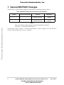
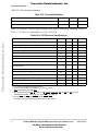
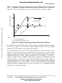
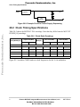
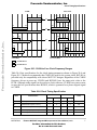
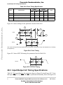
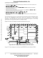
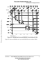
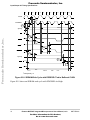
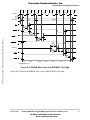
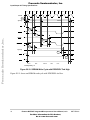
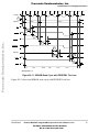
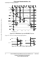
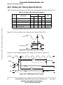
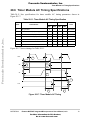
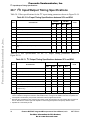
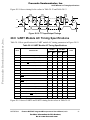
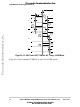
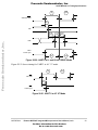
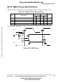
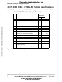
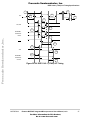
Freescale Semiconductor, Inc.
Addendum
MCF5407UMAD/D
Rev. 2, 2/2003
Freescale Semiconductor, Inc...
Errata to MCF5407 Integrated
Microprocessor User’s
Manual, rev 0
This errata describes corrections and updates to rev 0 of the MCF5407 ColdFire Integrated
Microprocessor User’s Manual, Motorola document order number MCF5407UM/D. The
General MCF5407 Changes section contains information that needs to be changed throughout
the book. Please check the world wide web at http://www.motorola.com/semiconductors for
the latest updates.
For More Information On This Product,
Go to: www.freescale.com
Freescale Semiconductor, Inc.
1. General MCF5407 Changes
The MCF5407 is offered with the temperature and frequency specifications shown in Table 1.
Freescale Semiconductor, Inc...
Table 1. MCF5407 Temperature and Frequency Specifications
Package
Operating Temperature
Frequency
MIPS Rating
208 plastic QFP
0 to 70° C
54 MHz max CLIN/
220 MHz max PCLK
316 Dhrystone MIPS at
220 MHz
208 plastic QFP
-40 to 85 ° C
54 MHz max CLKIN/
162 MHz max PCLK
233 Dhrystone MIPS at
162 MHz
NOTE
These specifications further amend the electrical characteristics described
in Section 1., “General MCF5407 Changes.”
The following section “Chapter 20, Electrical Specifications” replaces Chapter 20 of the MCF5407
ColdFire Integrated Microprocessor User’s Manual.
2
Errata to MCF5407 Integrated Microprocessor User’s Manual, rev 0
For More Information On This Product,
Go to: www.freescale.com
MOTOROLA
Freescale Semiconductor, Inc.
General Parameters
Chapter 20
Electrical Specifications
This chapter describes the AC and DC electrical specifications and thermal characteristics
for the MCF5407. Note that this information was correct at the time this book was
published. As process technologies improve, there is a likelihood that this information may
change. To confirm that this is the latest information, see Motorola’s ColdFire webpage,
http://www.motorola.com/coldfire.
Freescale Semiconductor, Inc...
20.1 General Parameters
Table 20-1 lists maximum and minimum ratings for supply and operating voltages and
storage temperature. Operating outside of these ranges may cause erratic behavior or
damage to the processor.
Table 20-1. Absolute Maximum Ratings
Rating
Symbol
Value
Units
External (I/O pads) supply voltage (3.3-V power pins)
EVcc
-0.3 to +4.0
V
Internal logic supply voltage
IVcc
-0.5 to +2.0 1, 2
V
PVcc
2, 3
V
PLL supply voltage
Internal logic supply voltage, input voltage level
Storage temperature range
Vin
Tstg
-0.5 to +2.0
-0.5 to +3.6
4
V
oC
-55 to +150
1
IVcc must not exceed EVcc
IVcc and PVcc must not differ by more than 0.5 V
3 PV must not exceed EV
cc
cc
4
Vin must not exceed EVcc
2
Table 20-2 lists junction and ambient operating temperatures.
Table 20-2. Operating Temperatures
Characteristic
Symbol
Value
Maximum operating junction temperature
Tj
95
o
C
Maximum operating junction temperature (Extended Temperature Device)
Tj
110
o
C
TAmax
70 1
o
C
Maximum operating ambient temperature (Extended Temperature Device)
TAmax
85
1
o
C
Minimum operating ambient temperature
TAmin
0
Minimum operating ambient temperature (Extended Temperature Device)
TAmin
-40
Maximum operating ambient temperature
1
Units
oC
o
C
This published maximum operating ambient temperature should be used only as a system design guideline. All
device operating parameters are guaranteed only when the junction temperature lies within the specified range.
MOTOROLA
Errata to MCF5407 Integrated Microprocessor User’s Manual, rev 0
For More Information On This Product,
Go to: www.freescale.com
3
Freescale Semiconductor, Inc.
General Parameters
Table 20-3 lists thermal resistances.
Table 20-3. Thermal Resistance
Characteristic
Symbol
Value
Junction to ambient
θJA
26.1
Junction to top reference
ψj
1.9
Units
o
C/W
oC/W
Table 20-4 lists DC electrical specifications. This table is based on an operating voltage of
EVcc = 3.3 Vdc ± 0.3 Vdc and IVcc of 1.8 ± 0.10 Vdc.
Freescale Semiconductor, Inc...
Table 20-4. DC Electrical Specifications
Characteristic
Symbol
Min
Max
Units
EVcc
3.0
3.6
V
IVcc
1.7
1.9
V
PVcc
1.65
1.95
V
Input high voltage 2
VIH
2.4
3.6
V
Input low voltage2
VIL
-0.5
0.5
V
Input signal undershoot
—
—
0.8
V
Input signal overshoot
—
—
0.8
V
Input leakage current @ 0.5/2.4 V during normal operation
Iin
—
20
µA
High impedance (three-state) leakage current @ 0.5/2.4 V during
normal operation
ITSI
—
20
µA
Signal low input current, VIL = 0.8 V 3
IIL
0
1
mA
IIH
0
1
mA
VOH
2.4
—
V
Output low voltage IOL = 6 mA 4, 12 mA 5
VOL
—
0.5
V
Load capacitance (all outputs)
CL
—
50
pF
CIN
—
TBD
pF
External (I/O pads) operation voltage range
Internal logic operation voltage range
PLL operation voltage range
1
Signal high input current, VIH = 2.0 V
Output high voltage IOH = 6 mA
6
4,
2
3
4
5
6
4
3
12 mA
Capacitance , Vin = 0 V, f = 1 MHz
1
1
5
IVcc and PVcc should be at the same voltage.
All pins except MTMOD. For MTMOD VIH = 2.6V, VIL = 0.4V.
BKPT/TMS, DSI/TDI, DSCLK/TRST
D[31:0], A[23:0], PP[15:0],TS, TA, SIZ[1:0], R/W, BR, BD, RSTO, AS, CS[7:0], BE[3:0], OE, PSTCLK,
PSTDDATA[7:0], DSO, TOUT[1:0], SCL, SDA, RTS[1:0], TXD[1:0]
BCLKO, RAS[1:0], CAS[3:0], DRAMW, SCKE, SRAS, SCAS
Capacitance CIN is periodically sampled rather than 100% tested.
Errata to MCF5407 Integrated Microprocessor User’s Manual, rev 0
For More Information On This Product,
Go to: www.freescale.com
MOTOROLA
Freescale Semiconductor, Inc.
General Parameters
20.1.1 Supply Voltage Sequencing and Separation Cautions
DC Power Supply Voltage
Freescale Semiconductor, Inc...
Figure 20-1 shows two situations to avoid in sequencing the IVcc and EVcc supplies.
EVcc
3.3V
2
1.8V
Supplies Stable
IVcc, PVcc
1
0
Time
Notes:
1
2
IVcc, PVcc rising before EVcc
EVcc rising much faster than IVcc, PVcc
Figure 20-1. Supply Voltage Sequencing and Separation Cautions
IVcc should not be allowed to rise early (1). This is usually avoided by running the regulator
for the IVcc supply (1.8 V) from the voltage generated by the 3.3-V EVcc supply
(Figure 20-2). This keeps IVcc from rising faster than EVcc.
IVcc should not rise so late that a large voltage difference is allowed between the two
supplies (2). Typically this situation is avoided by using external discrete diodes in series
between supplies as shown in Figure 20-2. The series diodes forward bias when the
difference between EVcc and IVcc reaches approximately 2.1V, causing IVcc to rise as EVcc
ramps up. When the IVcc regulator begins proper operation, the difference between
supplies should not exceed 1.5 V and conduction through the diode chain reduces to
essentially leakage current. During supply sequencing, the following general relationship
should be adhered to: EVcc Š IVcc Š (EVcc - 2.1 V). The PLL Vdd (PVcc) supply should
comply with these constraints just as IVcc does. In practice, PVcc is typically connected
directly to IVcc with some filtering.
MOTOROLA
Errata to MCF5407 Integrated Microprocessor User’s Manual, rev 0
For More Information On This Product,
Go to: www.freescale.com
5
Freescale Semiconductor, Inc.
Clock Timing Specifications
Supply
3.3 V
Regulator
EVcc
1.8 V
Regulator
IVcc, PVcc
Figure 20-2. Example Circuit to Control Supply Sequencing
Freescale Semiconductor, Inc...
20.2 Clock Timing Specifications
Table 20-5 shows the MCF5407 PLL encodings. Note that they differ from the MCF5307
DIVIDE[1:0] encodings.
Table 20-5. Divide Ratio Encodings
Input Clock (MHz)
D[2:0]/DIVIDE[2:0]
Core Clock (MHz)
PSTCLK (MHz)
Multiplier
162 MHz
220 MHz
162 MHz
00x–010
220 MHz
162 MHz
220 MHz
Reserved
011
40.0–54.0
40.0–55.0
3
120.0–162
120.0–165
60.0–81.0
60.0–82.5
100
25.0–40.5
25.0–55.0
4
100.0–162
100.0–220
50.0–81.0
50.0–110
101
25.0–32.4
25.0–44.0
5
125.0–162
125.0–220
67.5–81.0
67.5–110
110
25.0–27.0
25.0–36.6
6
150.0–162
150.0–220
75.0–81.0
75.0–110
111
Reserved
Figure 20-3 correlates CLKIN and core clock frequencies for the 3x–6x multipliers.
6
Errata to MCF5407 Integrated Microprocessor User’s Manual, rev 0
For More Information On This Product,
Go to: www.freescale.com
MOTOROLA
Freescale Semiconductor, Inc.
Clock Timing Specifications
CLKIN
Core Clock
40
54
120
162
120
165
3x
40
25
55
40.5
100
162
4x
25
55
Freescale Semiconductor, Inc...
25
100
220
125
32.4
162
5x
25
125
44
25 27
220
150
162
6x
25
36.6
25
30
35
220
150
40
45
50
CLKIN (MHz)
55
100 110 120 130 140 150 160 170 180 190 200 210 220
Core Clock (MHz)
162 MHz Device
220 MHz Device
Figure 20-3. CLKIN-to-Core Clock Frequency Ranges
Table 20-6 lists specifications for the clock timing parameters shown in Figure 20-4 and
Figure 20-5. Motorola recommends that CLKIN be used for the system clock. BCLKO is
provided only for compatibility with slower MCF5307 designs. Regardless of the CLKIN
frequency driven at power-up, CLKIN (and BCLKO) have the same ratio value to the
PCLK. Although either signal can be used as a clock reference, CLKIN leaves more room
to meet the bus specifications than BCLKO, which is generated as a phase-aligned signal
to CLKIN.
Table 20-6. Clock Timing Specification
162 MHz
Num
220 MHz
Characteristic
Units
Min
Max
Min
Max
18.5
Note 1
18.18
Note 1
nS
C1
CLKIN cycle time
C2
CLKIN rise time (0.5V to 2.4 V)
—
2
—
2
nS
C3
CLKIN fall time (2.4V to 0.5 V)
—
2
—
2
nS
C4
CLKIN duty cycle (at 1.5 V)
40
60
40
60
C5
MOTOROLA
PSTCLK cycle time
12.3
Note
1
9.1
Note
%
1
Errata to MCF5407 Integrated Microprocessor User’s Manual, rev 0
For More Information On This Product,
Go to: www.freescale.com
nS
7
Freescale Semiconductor, Inc.
Input/Output AC Timing Specifications
Table 20-6. Clock Timing Specification
162 MHz
Num
C6
Units
PSTCLK duty cycle (at 1.5 V)
C7
BCLKO cycle time
C8
BCLKO duty cycle (at 1.5 V)
C9
CLKIN to BCLKO
1
220 MHz
Characteristic
Min
Max
40
60
18.5
Note
1
Min
Max
40
60
18.18
Note
%
1
nS
45
55
45
55
%
-1.5
1.5
-1.5
1.5
nS
The PLL low-frequency limit depends on the clock divide ratio chosen. See Table 20-5.
Freescale Semiconductor, Inc...
Figure 20-4 shows timings for the parameters listed in Table 20-6.
C1
C3
C4
CLKIN
C4
C2
C7
C9
C8
BCLKO
C8
Note: Input and output AC timing specifications are measured to CLKIN with a 50-pF load capacitance (not including
pin capacitance).
Figure 20-4. Clock Timing
Figure 20-5 shows PSTCLK timings for parameters listed in Table 20-6.
C5
PSTCLK
C6
C6
Figure 20-5. PSTCLK Timing
20.3 Input/Output AC Timing Specifications
Table 20-7 lists specifications for parameters shown in Figure 20-6 and Figure 20-7. Note
that inputs IRQ[7,5,3,1], BKPT, and AS are synchronized internally; that is, the logic level
8
Errata to MCF5407 Integrated Microprocessor User’s Manual, rev 0
For More Information On This Product,
Go to: www.freescale.com
MOTOROLA
Freescale Semiconductor, Inc.
Input/Output AC Timing Specifications
is validated if the value does not change for two consecutive rising CLKIN edges. Setup
and hold times must be met only if recognition on a particular clock edge is required.
Table 20-7. Input AC Timing Specification
162 MHz
Num
Units
Min
Max
Min
Max
Valid to CLKIN rising (setup)
7.5 1, 8.5 2
—
7.51, 8.52
—
nS
CLKIN rising to invalid (hold)
1.0
—
1.0
—
nS
B3 3
Valid to CLKIN rising (setup)
0
—
0
—
nS
B4
3
CLKIN rising to invalid (hold)
0.5(C1) + 1.3
—
0.5(C1) + 1.3
—
nS
B5
4
CLKIN to input high impedance
—
2
—
2
Bus clock
CLKIN to EDGESEL delay
0
5.0
0
5.0
nS
B1
B2
Freescale Semiconductor, Inc...
220 MHz
Characteristic
1
B6
1
Inputs: BG, TA, A[23:0], PP[15:0], SIZ[1:0], R/W, TS, EDGESEL, D[31:0], and BKPT
Inputs IRQ[7,5,3,1]
3
Inputs: AS
4
Inputs: D[31:0]
2
Table 20-8 lists specifications for timings in Figure 20-6, Figure 20-7, and Figure 20-13.
Although output signals that share a specification number have approximately the same
timing, due to loading differences, they do not necessarily change at the same time.
However, they have similar timings; that is, minimum and maximum times are not mixed.
Table 20-8. Output AC Timing Specification
162 MHz
Num
220 MHz
Characteristic
B10 1, 2, 3 CLKIN rising to valid
B11 3,4,5
CLKIN rising to invalid
(hold)
B12 6, 7
CLKIN to high impedance
(three-state)
B13 8,2,3
CLKIN rising to valid
B14 8,2,3
CLKIN rising to invalid
(hold)
B15 2,3
Units
Min
Max
Min
Max
—
10.5 4
—
10.54
nS
—
5
nS
—
12.5 5
1.0 5
—
1.0 5
—
nS
—
10
—
10
nS
—
0.5(C1) +10.5 9
—
0.5(C1) +10.59
nS
—
10
—
+12.510
nS
12.5
0.5(C1) +12.5
0.5(C1)
0.5(C1) + 1.0
—
0.5(C1) + 1.0
—
nS
EDGESEL to valid
—
12
—
12
nS
EDGESEL to invalid (hold)
2
—
2
—
nS
H1
HIZ to high impedance
—
60
—
60
nS
H2
HIZ to low Impedance
—
60
—
60
nS
B16
2,3
1
Outputs that change only on rising edge of CLKIN: RSTO, TS, BR, BD, TA, R/W, SIZ[1:0], PP[7:0] (and PP[15:8]
when configured as parallel port outputs).
2 Outputs that can change on either CLKIN edge depending only on EDGESEL: D[31:0], A[23:0], SCKE, SRAS,
SCAS, and DRAMW and on PP[15:8] when individually configured as A[31:24] outputs.
MOTOROLA
Errata to MCF5407 Integrated Microprocessor User’s Manual, rev 0
For More Information On This Product,
Go to: www.freescale.com
9
Freescale Semiconductor, Inc.
Input/Output AC Timing Specifications
3
4
5
6
7
8
9
Freescale Semiconductor, Inc...
10
Outputs that can change on either CLKIN edge depending upon EDGESEL and the interface operating mode
(DRAM/SDRAM): RAS[1:0], CAS[3:0]
SRAS, SCAS, DRAMW, RAS[1:0], CAS[3:0]
D[31:0], A[23:0], TM[2:0], TT[1:0], SIZ[1:0], R/W, TIP, TS, BR, BD, and TA and PP[15:8] when individually
configured as A[31:24] outputs.
High impedance (three-state): D[31:0]
Outputs that transition to high impedance due to bus arbitration: A[23:0], R/W, SIZ[1:0], TS, AS, and TA, and
PP[15:8] when individually configured as A[31:24] outputs.
Outputs that change only on falling edge of CLKIN: AS, CS[7:0], BE[3:0], OE
SRAS, SCAS, DRAMW, RAS[1:0], CAS[3:0], AS, CS[7:0], BE[3:0], OE
D[31:0], A[23:0], TM[2:0], TT[1:0], SIZ[1:0], R/W, TIP, and TS and on PP[15:8] when individually configured as
A[31:24] outputs.
Note that these figures show two representative bus operations and do not attempt to show
all cases. For explanations of the states, S0–S5, see Section 18.4, “Data Transfer
Operation.” Note that Figure 20-7 does not show all signals that apply to each timing
specification. See the previous tables for a complete listing.
Figure 20-6 shows AC timings for normal read and write bus cycles.
S0
CLKIN
S1
S2
S3
S4
S5
S0
S1
S2
S3
S4
S5
B11
B10
A[31:0]
TM[2:0]
TT[1:0]
SIZ[1:0]
R/W
B11
TS
TIP
B14
B13
AS, CS, OE
BE/BWE[3:0]
B12
B2
B10
D[31:0]
B1
B5
TA
Figure 20-6. AC Timings—Normal Read and Write Bus Cycles
Figure 20-7 shows timings for a read cycle with EDGESEL tied to buffered CLKIN.
10
Errata to MCF5407 Integrated Microprocessor User’s Manual, rev 0
For More Information On This Product,
Go to: www.freescale.com
MOTOROLA
Freescale Semiconductor, Inc.
Input/Output AC Timing Specifications
0
1
2
3
4
5
6
7
8
9
10
11
12
13
14
CLKIN
B6
EDGESEL
B15
Row
A[31:0]
Column
TS
Freescale Semiconductor, Inc...
B16
SRAS
B15
SCAS 1
B16
DRAMW
B1
D[31:0]
B16
B2
RAS
B16
CAS
ACTV
1 DACR[CASL]
NOP
READ
NOP
NOP
PALL
NOP
=2
Figure 20-7. SDRAM Read Cycle with EDGESEL Tied to Buffered CLKIN
Figure 20-8 shows an SDRAM write cycle with EDGESEL tied to buffered CLKIN.
MOTOROLA
Errata to MCF5407 Integrated Microprocessor User’s Manual, rev 0
For More Information On This Product,
Go to: www.freescale.com
11
Freescale Semiconductor, Inc.
Input/Output AC Timing Specifications
0
1
2
3
4
5
6
7
8
9
10
11
12
CLKIN
B6
EDGESEL
B15
Row
A[31:0]
Column
Freescale Semiconductor, Inc...
TS
B16
SRAS
B15
SCAS 1
B16
DRAMW
B15
D[31:0]
B16
RAS
B16
CAS
NOP
ACTV
1 DACR[CASL]
WRITE
NOP
PALL
=2
Figure 20-8. SDRAM Write Cycle with EDGESEL Tied to Buffered CLKIN
Figure 20-9 shows an SDRAM read cycle with EDGESEL tied high.
12
Errata to MCF5407 Integrated Microprocessor User’s Manual, rev 0
For More Information On This Product,
Go to: www.freescale.com
MOTOROLA
Freescale Semiconductor, Inc.
Input/Output AC Timing Specifications
0
1
2
3
4
5
6
7
8
9
10
11
12
13
14
15
CLKIN
B10
Row
A[31:0]
Column
TS
B11
SRAS
Freescale Semiconductor, Inc...
B10
SCAS 1
B11
DRAMW
B1
D[31:0]
B11
B2
RAS
B11
CAS
ACTV
1 DACR[CASL]
NOP
READ
NOP
NOP
PALL
=2
Figure 20-9. SDRAM Read Cycle with EDGESEL Tied High
Figure 20-10 shows an SDRAM write cycle with EDGESEL tied high.
MOTOROLA
Errata to MCF5407 Integrated Microprocessor User’s Manual, rev 0
For More Information On This Product,
Go to: www.freescale.com
13
Freescale Semiconductor, Inc.
Input/Output AC Timing Specifications
0
1
2
3
4
5
6
7
8
9
10
11
12
CLKIN
B10
Row
A[31:0]
Column
TS
B11
SRAS
Freescale Semiconductor, Inc...
B10
SCAS1
B11
DRAMW
B10
D[31:0]
B11
RAS
B11
CAS
ACTV
1
NOP
WRITE
NOP
PALL
DACR[CASL] = 2
Figure 20-10. SDRAM Write Cycle with EDGESEL Tied High
Figure 20-11 shows an SDRAM read cycle with EDGESEL tied low.
14
Errata to MCF5407 Integrated Microprocessor User’s Manual, rev 0
For More Information On This Product,
Go to: www.freescale.com
MOTOROLA
Freescale Semiconductor, Inc.
Input/Output AC Timing Specifications
0
1
2
3
4
5
6
7
8
9
10
11
12
13
14
15
CLKIN
B13
Row
A[31:0]
Column
TS
B14
SRAS
Freescale Semiconductor, Inc...
B13
SCAS1
B14
DRAMW
B1
D[31:0]
B14
B2
RAS
B14
CAS
ACTV
1 DACR[CASL]
NOP
READ
NOP
NOP
PALL
=2
Figure 20-11. SDRAM Read Cycle with EDGESEL Tied Low
Figure 20-12 shows an SDRAM write cycle with EDGESEL tied low.
MOTOROLA
Errata to MCF5407 Integrated Microprocessor User’s Manual, rev 0
For More Information On This Product,
Go to: www.freescale.com
15
Freescale Semiconductor, Inc.
Input/Output AC Timing Specifications
0
1
2
3
4
5
6
7
8
9
10
11
12
CLKIN
B13
Row
A[31:0]
Column
TS
B14
SRAS
Freescale Semiconductor, Inc...
B13
SCAS1
B14
DRAMW
B13
D[31:0]
B14
RAS
B14
CAS
ACTV
1 DACR[CASL]
NOP
WRITE
NOP
PALL
=2
Figure 20-12. SDRAM Write Cycle with EDGESEL Tied Low
Figure 20-13 shows AC timing showing high impedance.
HIZ
H1
H2
OUTPUTS
Figure 20-13. AC Output Timing—High Impedance
16
Errata to MCF5407 Integrated Microprocessor User’s Manual, rev 0
For More Information On This Product,
Go to: www.freescale.com
MOTOROLA
Freescale Semiconductor, Inc.
Reset Timing Specifications
20.4 Reset Timing Specifications
Table 20-9 lists specifications for the reset timing parameters shown in Figure 20-14.
Table 20-9. Reset Timing Specification
162 MHz
Num
Units
Min
Max
Min
Max
R1 1
Valid to CLKIN (setup)
7.5
—
7.5
—
nS
R2
CLKIN to invalid (hold)
1.0
—
1.0
—
nS
R3
RSTI to invalid (hold)
1.0
—
1.0
—
nS
1
Freescale Semiconductor, Inc...
220 MHz
Characteristic
RSTI and D[7:0] are synchronized internally. Setup and hold times must be met only if
recognition on a particular clock is required.
Figure 20-14 shows reset timing for the values in Table 20-9.
CLKIN
R1
RSTI
R2
D[7:0]
R1
R3
Note: Mode selects are registered on the rising CLKIN edge before the cycle in which RSTI is
recognized as being negated.
Figure 20-14. Reset Timing
MOTOROLA
Errata to MCF5407 Integrated Microprocessor User’s Manual, rev 0
For More Information On This Product,
Go to: www.freescale.com
17
Freescale Semiconductor, Inc.
Debug AC Timing Specifications
20.5 Debug AC Timing Specifications
Table 20-10 lists specifications for the debug AC timing parameters shown in Figure 20-16.
Table 20-10. Debug AC Timing Specification
162 MHz
Num
Max
Min
Max
PSTDDATA to PSTCLK setup
—
4.5
—
3
nS
D2
PSTCLK to PSTDDATA hold
—
4.5
—
3
nS
DSI-to-DSCLK setup
1
—
1
—
PSTCLKs
DSCLK-to-DSO hold
4
—
4
—
PSTCLKs
DSCLK cycle time
5
—
5
—
PSTCLKs
D4
Freescale Semiconductor, Inc...
Units
Min
D1
D3
1
D5
1
220 MHz
Characteristic
DSCLK and DSI are synchronized internally. D4 is measured from the synchronized DSCLK
input relative to the rising edge of PSTCLK.
Figure 20-15 shows real-time trace timing for the values in Table 20-10.
PSTCLK
D1
D2
PSTDDATA[7:0]
Figure 20-15. Real-Time Trace AC Timing
Figure 20-16 shows BDM serial port AC timing for the values in Table 20-10.
PSTCLK
D5
DSCLK
D3
DSI
Current
Next
D4
DSO
Past
Current
Figure 20-16. BDM Serial Port AC Timing
18
Errata to MCF5407 Integrated Microprocessor User’s Manual, rev 0
For More Information On This Product,
Go to: www.freescale.com
MOTOROLA
Freescale Semiconductor, Inc.
Timer Module AC Timing Specifications
20.6 Timer Module AC Timing Specifications
Table 20-11 lists specifications for timer module AC timing parameters shown in
Figure 20-17.
Table 20-11. Timer Module AC Timing Specification
162 MHz
Freescale Semiconductor, Inc...
Num
220 MHz
Characteristic
Units
Min
Max
Min
Max
3
—
3
—
Bus clocks
T1
TIN cycle time
T2
TIN valid to CLKIN (input setup)
7.5
—
7.5
—
nS
T3
CLKIN to TIN invalid (input hold)
1.0
—
1.0
—
nS
T4
CLKIN to TOUT valid (output valid)
—
12
—
12
nS
T5
CLKIN to TOUT invalid (output hold)
1.0
—
1.0
—
nS
T6
TIN pulse width
1
—
1
—
Bus clocks
T7
TOUT pulse width
1
—
1
—
Bus clocks
Figure 20-17 shows timings for Table 20-11.
CLKIN
T6
TIN
T2
T3
TIN
T1
T7
TOUT
T4
T5
Figure 20-17. Timer Module AC Timing
MOTOROLA
Errata to MCF5407 Integrated Microprocessor User’s Manual, rev 0
For More Information On This Product,
Go to: www.freescale.com
19
Freescale Semiconductor, Inc.
I2C Input/Output Timing Specifications
20.7 I2C Input/Output Timing Specifications
Table 20-12 lists specifications for the I2C input timing parameters shown in Figure 20-18.
Table 20-12. I2C Input Timing Specifications between SCL and SDA
162 MHz
Freescale Semiconductor, Inc...
Num
220 MHz
Characteristic
Units
Min
Max
Min
Max
I1
Start condition hold time
2
—
2
—
Bus clocks
I2
Clock low period
8
—
8
—
Bus clocks
I3
SCL/SDA rise time (VIL = 0.5 V to VIH = 2.4 V)
—
1
—
1
mS
I4
Data hold time
0
—
0
—
nS
I5
SCL/SDA fall time (VIH = 2.4 V to VIL = 0.5 V)
—
1
—
1
mS
I6
Clock high time
4
—
4
—
Bus clocks
I7
Data setup time
0
—
0
—
nS
I8
Start condition setup time (for repeated start condition
only)
2
—
2
—
Bus clocks
I9
Stop condition setup time
2
—
2
—
Bus clocks
Table 20-13 lists specifications for the I2C output timing parameters shown in
Figure 20-18.
Table 20-13. I2C Output Timing Specifications between SCL and SDA
162 MHz
Num
I1 1
I2
I3
1
2
I4 1
220 MHz
Characteristic
Units
Min
Max
Min
Max
Start condition hold time
6
—
6
—
Bus clocks
Clock low period
10
—
10
—
Bus clocks
Note 2
Note 2
Note 2
Note 2
SCL/SDA rise time (VIL = 0.5 V to VIH = 2.4 V)
Data hold time
7
—
7
—
Bus clocks
I5
3
SCL/SDA fall time (VIH = 2.4 V to VIL = 0.5 V)
—
3
—
3
nS
I6
1
Clock high time
10
—
10
—
Bus clocks
I7
1
Data setup time
2
—
2
—
Bus clocks
I8 1
Start condition setup time (for repeated start
condition only)
20
—
20
—
Bus clocks
I9 1
Stop condition setup time
10
—
10
—
Bus clocks
1
Programming IFDR with the maximum frequency (IFDR = 0x20) results in the minimum output timings listed here.
The I2C interface is designed to scale the data transition time, moving it to the middle of the SCL low period. The
actual position is affected by the prescale and division values programmed in IFDR.
2 Because SCL and SDA are open-collector-type outputs, which the processor can only actively drive low, the time
SCL or SDA takes to reach a high level depends on external signal capacitance and pull-up resistor values.
3
Specified at a nominal 50-pF load.
20
Errata to MCF5407 Integrated Microprocessor User’s Manual, rev 0
For More Information On This Product,
Go to: www.freescale.com
MOTOROLA
Freescale Semiconductor, Inc.
UART Module AC Timing Specifications
Figure 20-18 shows timing for the values in Table 20-12 and Table 20-13.
I2
I6
I5
SCL
I1
I4
I3
I8
I9
I7
SDA
Freescale Semiconductor, Inc...
Figure 20-18. I2C Input/Output Timings
20.8 UART Module AC Timing Specifications
Table 20-14 lists specifications for UART module AC timing parameters in Figure 20-19.
Table 20-14. UART Module AC Timing Specifications
162 MHz
Num
220 MHz
Characteristic
Units
Min
Max
Min
Max
U1
RXD valid to CLKIN (input setup)
7.5
—
7.5
—
nS
U2
CLKIN to RXD invalid (input hold)
1.0
—
1.0
—
nS
U3
CTS valid to CLKIN (input setup)
7.5
—
7.5
—
nS
U4
CLKIN to CTS invalid (input hold)
1.0
—
1.0
—
nS
U5
CLKIN to TXD valid (output valid)
—
12
—
12
nS
U6
CLKIN to TXD invalid (output hold)
1.0
—
1.0
—
nS
U7
CLKIN to RTS valid (output valid)
—
12
—
12
nS
U8
CLKIN to RTS invalid (output hold)
1.0
—
1.0
—
nS
U9
CTS high time
38
—
38
—
nS
U10
CTS low time
38
—
38
—
nS
U11
CTS rising to TxD valid
—
20
—
20
nS
U12
RxD setup to CTS falling
10
—
10
—
nS
U13
RxD hold from CTS falling
—
5
—
5
nS
U14
TxD to RxD (remote loop back)
—
15
—
15
nS
U15
TIN1 setup to CTS falling
10
—
10
—
nS
U16
TIN1 hold from CTS falling
—
5
—
5
nS
U17
CTS rising to RTS asserted
—
20
—
20
nS
Figure 20-19 shows UART0 and UART1 timing for the values in Table 20-14.
MOTOROLA
Errata to MCF5407 Integrated Microprocessor User’s Manual, rev 0
For More Information On This Product,
Go to: www.freescale.com
21
Freescale Semiconductor, Inc.
UART Module AC Timing Specifications
CLKIN
U1
RXD
U2
U3
Freescale Semiconductor, Inc...
CTS
U4
U5
TXD
U6
U7
RTS
U8
Figure 20-19. UART0 and UART1 Module AC Timing—UART Mode
Figure 20-19 shows timing for UART1 in 8- and 16-bit CODEC mode.
22
Errata to MCF5407 Integrated Microprocessor User’s Manual, rev 0
For More Information On This Product,
Go to: www.freescale.com
MOTOROLA
Freescale Semiconductor, Inc.
UART Module AC Timing Specifications
U9
U10
CTS/
Serial bit clock
U11
TxD
Freescale Semiconductor, Inc...
U14
U12
U13
RxD
TIN1/
Frame sync
U15
U16
Figure 20-20. UART1 in 8- and 16-bit CODEC Mode
Figure 20-21 shows timing for UART1 in AC ‘97 mode.
U9
U10
CTS/
Bit clock
U17
RTS/
Frame sync
Figure 20-21. UART1 in AC ‘97 Mode
MOTOROLA
Errata to MCF5407 Integrated Microprocessor User’s Manual, rev 0
For More Information On This Product,
Go to: www.freescale.com
23
Freescale Semiconductor, Inc.
Parallel Port (General-Purpose I/O) Timing Specifications
20.9 Parallel Port (General-Purpose I/O) Timing
Specifications
Table 20-15 lists specifications for general-purpose I/O timing parameters in Figure 20-22.
Table 20-15. General-Purpose I/O Port AC Timing Specifications
162 MHz
Freescale Semiconductor, Inc...
Num
220 MHz
Characteristic
Units
Min
Max
Min
Max
P1
PP valid to CLKIN (input setup)
7.5
—
7.5
—
nS
P2
CLKIN to PP invalid (input hold)
1.0
—
1.0
—
nS
P3
CLKIN to PP valid (output valid)
—
12.5
—
12.5
nS
P4
CLKIN to PP invalid (output hold)
1.0
—
1.0
—
nS
Figure 20-22 shows general-purpose I/O timing.
CLKIN
P1
PP IN
P2
P3
PP OUT
P4
Figure 20-22. General-Purpose I/O Timing
24
Errata to MCF5407 Integrated Microprocessor User’s Manual, rev 0
For More Information On This Product,
Go to: www.freescale.com
MOTOROLA
Freescale Semiconductor, Inc.
DMA Timing Specifications
20.10 DMA Timing Specifications
Table 20-15 lists specifications for DMA timing parameters shown in Figure 20-22.
Table 20-16. DMA AC Timing Specifications
162 MHz
Freescale Semiconductor, Inc...
Num
220 MHz
Characteristic
Units
Min
Max
Min
Max
M1
DREQ valid to CLKIN (input setup)
7.5
—
7.5
—
nS
M2
CLKIN to DREQ invalid (input hold)
1.0
—
1.0
—
nS
M3
CLKIN to DACK valid (output valid)
—
10
—
10
nS
M4
CLKIN to DACK invalid (output hold)
1.0
—
1.0
—
nS
Figure 20-23 shows DMA AC timing.
CLKIN
M1
DREQ
M4
M2
M3
DACK
Figure 20-23. DMA Timing
MOTOROLA
Errata to MCF5407 Integrated Microprocessor User’s Manual, rev 0
For More Information On This Product,
Go to: www.freescale.com
25
Freescale Semiconductor, Inc.
IEEE 1149.1 (JTAG) AC Timing Specifications
20.11 IEEE 1149.1 (JTAG) AC Timing Specifications
Table 20-17 lists specifications for JTAG AC timing parameters shown in Figure 20-24.
Table 20-17. IEEE 1149.1 (JTAG) AC Timing Specifications
Freescale Semiconductor, Inc...
Num
Characteristic
All
Frequencies
Units
Min
Max
0
10
MHz
—
TCK frequency of operation
J1
TCK cycle time
100
—
nS
J2a
TCK clock pulse high width (measured at 1.5 V)
40
—
nS
J2b
TCK clock pulse low width (measured at 1.5 V)
40
—
nS
J3a
TCK fall time (VIH = 2.4 V to VIL = 0.5V)
—
5
nS
J3b
TCK rise time (VIL = 0.5v to VIH = 2.4V)
—
5
nS
J4
TDI, TMS to TCK rising (input setup)
10
—
nS
J5
TCK rising to TDI, TMS invalid (hold)
15
—
nS
J6
Boundary scan data valid to TCK (setup)
10
—
nS
J7
TCK to boundary-scan data invalid (hold)
15
—
nS
J8
TRST pulse width (asynchronous to clock edges)
15
—
—
J9
TCK falling to TDO valid (signal from driven or
three-state)
—
30
nS
J10
TCK falling to TDO high impedance
—
30
nS
J11
TCK falling to boundary scan data valid (signal from
driven or three-state)
—
30
nS
J12
TCK falling to boundary scan data high impedance
—
30
nS
Figure 20-24 shows JTAG timing.
26
Errata to MCF5407 Integrated Microprocessor User’s Manual, rev 0
For More Information On This Product,
Go to: www.freescale.com
MOTOROLA
Freescale Semiconductor, Inc.
IEEE 1149.1 (JTAG) AC Timing Specifications
J3a
J1
TCK
J2b
J2a
J3b
J4
TDI, TMS
J5
J6
Freescale Semiconductor, Inc...
BOUNDARY
SCAN DATA
INPUT
J7
TRST
J8
J9
TDO
J10
BOUNDARY
SCAN DATA
OUTPUT
J11
J12
Figure 20-24. IEEE 1149.1 (JTAG) AC Timing
MOTOROLA
Errata to MCF5407 Integrated Microprocessor User’s Manual, rev 0
For More Information On This Product,
Go to: www.freescale.com
27
Freescale Semiconductor, Inc.
HOW TO REACH US:
USA/EUROPE/LOCATIONS NOT LISTED:
Motorola Literature Distribution
P.O. Box 5405, Denver, Colorado 80217
1-303-675-2140 or 1-800-441-2447
JAPAN:
Freescale Semiconductor, Inc...
Motorola Japan Ltd.
SPS, Technical Information Center
3-20-1, Minami-Azabu Minato-ku
Tokyo 106-8573 Japan
81-3-3440-3569
Information in this document is provided solely to enable system and software implementers to use
ASIA/PACIFIC:
Motorola products. There are no express or implied copyright licenses granted hereunder to design
Motorola Semiconductors H.K. Ltd.
Silicon Harbour Centre, 2 Dai King Street
Tai Po Industrial Estate, Tai Po, N.T., Hong Kong
852-26668334
or fabricate any integrated circuits or integrated circuits based on the information in this document.
TECHNICAL INFORMATION CENTER:
use of any product or circuit, and specifically disclaims any and all liability, including without
1-800-521-6274
limitation consequential or incidental damages. “Typical” parameters which may be provided in
HOME PAGE:
Motorola reserves the right to make changes without further notice to any products herein.
Motorola makes no warranty, representation or guarantee regarding the suitability of its products
for any particular purpose, nor does Motorola assume any liability arising out of the application or
Motorola data sheets and/or specifications can and do vary in different applications and actual
performance may vary over time. All operating parameters, including “Typicals” must be validated
http://www.motorola.com/semiconductors
for each customer application by customer’s technical experts. Motorola does not convey any
DOCUMENT COMMENTS:
license under its patent rights nor the rights of others. Motorola products are not designed,
FAX (512) 933-2625
Attn: TECD Applications Engineering
intended, or authorized for use as components in systems intended for surgical implant into the
body, or other applications intended to support or sustain life, or for any other application in which
the failure of the Motorola product could create a situation where personal injury or death may
occur. Should Buyer purchase or use Motorola products for any such unintended or unauthorized
application, Buyer shall indemnify and hold Motorola and its officers, employees, subsidiaries,
affiliates, and distributors harmless against all claims, costs, damages, and expenses, and
reasonable attorney fees arising out of, directly or indirectly, any claim of personal injury or death
associated with such unintended or unauthorized use, even if such claim alleges that Motorola was
negligent regarding the design or manufacture of the part.
Motorola and the Stylized M Logo are registered in the U.S. Patent and Trademark Office.
digital dna is a trademark of Motorola, Inc. All other product or service names are the property of
their respective owners. Motorola, Inc. is an Equal Opportunity/Affirmative Action Employer.
© Motorola, Inc. 2003
MCF5407UMAD/D
For More Information On This Product,
Go to: www.freescale.com