1
TLE983x
Application Hints
Application Note
Rev. 1.1, 2013-06-01
Automotive Power
TLE983x
Application Hints
Table of Contents
1
Abstract . . . . . . . . . . . . . . . . . . . . . . . . . . . . . . . . . . . . . . . . . . . . . . . . . . . . . . . . . . . . . . . . . . . . . . . . 3
2
Introduction . . . . . . . . . . . . . . . . . . . . . . . . . . . . . . . . . . . . . . . . . . . . . . . . . . . . . . . . . . . . . . . . . . . . . 3
3
3.1
3.2
3.3
3.4
3.5
3.6
3.7
3.8
3.9
3.10
3.11
3.12
3.13
3.14
3.15
3.16
3.17
3.18
3.19
Collection of Topics . . . . . . . . . . . . . . . . . . . . . . . . . . . . . . . . . . . . . . . . . . . . . . . . . . . . . . . . . . . . . . 4
Flashing of the NVM when the Device is in Fail-Safe Sleep Mode . . . . . . . . . . . . . . . . . . . . . . . . . . . . 4
Behavior of Power Modules while Startup / Undervoltage . . . . . . . . . . . . . . . . . . . . . . . . . . . . . . . . . . 4
LIN-Transceiver disabled with slow Ramping of VS . . . . . . . . . . . . . . . . . . . . . . . . . . . . . . . . . . . . . . . 5
XSFR WAKE_STS_MON doesn’t have its Reset Value 00H after Power On Reset (POR) . . . . . . . . . 6
Temperature Calculation . . . . . . . . . . . . . . . . . . . . . . . . . . . . . . . . . . . . . . . . . . . . . . . . . . . . . . . . . . . 6
Low Side Switch (LSS) Current Calculation . . . . . . . . . . . . . . . . . . . . . . . . . . . . . . . . . . . . . . . . . . . . . 6
Proper Handling of Assembly Buffer . . . . . . . . . . . . . . . . . . . . . . . . . . . . . . . . . . . . . . . . . . . . . . . . . . 7
VAREF Short to Ground . . . . . . . . . . . . . . . . . . . . . . . . . . . . . . . . . . . . . . . . . . . . . . . . . . . . . . . . . . . . 9
UART Lock-Up Behavior . . . . . . . . . . . . . . . . . . . . . . . . . . . . . . . . . . . . . . . . . . . . . . . . . . . . . . . . . . . 9
After leaving Stop Mode, the Flash is protected . . . . . . . . . . . . . . . . . . . . . . . . . . . . . . . . . . . . . . . . . 10
After leaving Stop Mode, Address of ECC Error is lost . . . . . . . . . . . . . . . . . . . . . . . . . . . . . . . . . . . 10
Stop Mode while ADC is running . . . . . . . . . . . . . . . . . . . . . . . . . . . . . . . . . . . . . . . . . . . . . . . . . . . . 10
VDDEXT doesn’t Switch Off in Case of an Overload . . . . . . . . . . . . . . . . . . . . . . . . . . . . . . . . . . . . . 11
MI_CLK and CLK_2MHz Adaption to System Clock . . . . . . . . . . . . . . . . . . . . . . . . . . . . . . . . . . . . . 11
Use of external Oscillator as Clock Source . . . . . . . . . . . . . . . . . . . . . . . . . . . . . . . . . . . . . . . . . . . . 12
Usage of Paging in the TLE983x . . . . . . . . . . . . . . . . . . . . . . . . . . . . . . . . . . . . . . . . . . . . . . . . . . . . 14
ADC1 Calibration . . . . . . . . . . . . . . . . . . . . . . . . . . . . . . . . . . . . . . . . . . . . . . . . . . . . . . . . . . . . . . . . 14
Enabling of the Memory Protection . . . . . . . . . . . . . . . . . . . . . . . . . . . . . . . . . . . . . . . . . . . . . . . . . . . 16
LIN Slope Mode Setting . . . . . . . . . . . . . . . . . . . . . . . . . . . . . . . . . . . . . . . . . . . . . . . . . . . . . . . . . . . 17
4
Conclusion . . . . . . . . . . . . . . . . . . . . . . . . . . . . . . . . . . . . . . . . . . . . . . . . . . . . . . . . . . . . . . . . . . . . 19
5
Additional Information . . . . . . . . . . . . . . . . . . . . . . . . . . . . . . . . . . . . . . . . . . . . . . . . . . . . . . . . . . . 19
6
Revision History . . . . . . . . . . . . . . . . . . . . . . . . . . . . . . . . . . . . . . . . . . . . . . . . . . . . . . . . . . . . . . . . 20
Application Note
2
Rev. 1.1, 2013-06-01
TLE983x
Application Hints
Abstract
1
Abstract
Note: The following information is given as a hint for the implementation of the device only and shall not be
regarded as a description or warranty of a certain functionality, condition or quality of the device.
This Application Note is intended to provide helpful suggestions and hints how to set up and handle specific
modules and functionalities which are not subject of the Users Manual or Data Sheet and might be interesting for
end users. It is organized in a frequently asked question style and doesn’t follow any specific order.
2
Introduction
This Application Note lists topics which emerged from frequently asked questions of users or from changed user
requirements. Each topic is organized in three sections:
•
•
•
Topic:
– Short description of the issue.
Description:
– Statement why this topic appeared
Implementation hint:
– Instruction how to handle this topic
Application Note
3
Rev. 1.1, 2013-06-01
TLE983x
Application Hints
Collection of Topics
3
Collection of Topics
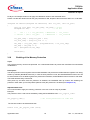
3.1
Flashing of the NVM when the Device is in Fail-Safe Sleep Mode
Topic:
In fail-safe Sleep Mode the TLE983x can not be flashed.
Description:
In case of a not properly served watchdog, the TE983x is reset. After five resets the device goes to Sleep Mode
and can not be flashed anymore.
Implementation hint:
•
•
Connect the reset pin with the MON1 pin. Turn VS to below 10 V, e.g. 8V. Then flashing via DAP is possible.
When a reset occurs (e.g. not served watchdog) the reset pin is toggled actively. The MON1 pin is a high
voltage monitor pin and the toggling of the MON1 pin wakes the devices up. That way the TLE983x stays
awake and can be flashed. The high level of the MON1 pin is VS/2 and the reset pin has a TTL level of 5V.
Therefore VS has to be clearly below 10V, then the TTL high signal is recognized as high level.
A second possibility to prevent that the device goes to Sleep Mode is to pull the LIN pin to GND. This also
keeps the devices awake and flashing is possible.
3.2
Behavior of Power Modules while Startup / Undervoltage
Topic:
The functional range of the TLE983x in Active Mode is defined for a supply voltage of VS = 5.5 – 27V. Outside of
this range the behavior of the power modules (LIN Transceiver, Monitor Inputs) cannot be guaranteed.
Description:
The functional range of the microcontroller and flash module within the TLE983x is defined for a supply voltage in
Active Mode with VS = 3.0 – 27V. The program execution of the microcontroller (e.g. initialization code) starts
already with VS = 3.0V. Therefore the software initialization of the power modules can occur inside the VS range
VS = 3.0 – 27V. This may lead to an undefined behavior of the power modules also inside the VS range
VS = 5.5 – 27V, which is the range of full functionality.
The detailed time of the power module initialization by software is influenced and may differ significantly by the
following characteristics:
•
•
•
Slew rate of VS
Disturbance and
Location of initialization code for power modules (early or later execution)
Implementation hint:
Therefore it is highly recommended to synchronize the power module initialization with the bit VS_UV_STS in the
Register SYS_SUPPLY_STS. The initialization of the power modules should only occur when VS_UV_STS is set
to 0B (no undervoltage interrupt occurred). Re-initialization of the power modules (LIN Transceiver, Monitor Inputs)
should be done whenever an undervoltage interrupt occurred (voltage drop below 5.5V).
Application Note
4
Rev. 1.1, 2013-06-01
TLE983x
Application Hints
Collection of Topics
3.3
LIN-Transceiver disabled with slow Ramping of VS
Topic:
The LIN-Transceiver stays disabled with slow ramping of VS.
Description:
After a reset the PCU_CTRL_STS_2 register is set to a value which disables the LIN-Transceiver for the time
whenever the VS under voltage condition is met (VS < 5.5V). It has to be ensured by software sequence, that only
after leaving the VS under voltage condition (VS > 5.5V), which can be checked by software, the LIN module will
be properly enabled.
Implementation hint:
Software activities to meet this requirement:
•
•
•
Initialization Code to check whether VS is within the specified range of at least VS = 5.5 – 27V
SYS_SUPPLY_STS.VS_UV_STS to be checked == 0B
Afterwards the register LIN_CTRL_STS_1 has to be programmed to the value 00H and afterwards to 06H
Programming Example:
if ((SYS_SUPPLY_STS & 0x02) == 0x00)
//reset LIN OC flag
{
LIN_CTRL_STS_1 = (uint8)0;
LIN_CTRL_STS_1 = (uint8)6;
//reset LIN OC flag
//set LIN_CTRL_STS_1 back to reset state
}
After this initialization the LIN-Communication can start. In order to avoid any effects of unpredictable voltage
drops, the register LIN_CTRL_STS_1 should be set in advance of any LIN transmission in a sequence first to 00H
and afterwards to 06H.
Exceptions:
For startup sequences the under voltage condition has been combined with the LIN Receiver Overcurrent Status
(bit LIN_OC_STS in register LIN_CTRL_STS_1 is also set to 1B). This is an unintended behavior. This issue is
also covered with the previous described software sequence.
•
•
•
In TLE983x, Step BD the OC status bit will be set, but the LIN-Transceiver will not be switched off
In TLE983x, Step BC the behavior has been verified and validated
In TLE983x, Step BB the LIN Receiver Overcurrent Status has not been enabled
Outside the functional range the behavior of the power modules (e.g. LIN Transceiver, Monitor Inputs) cannot be
guaranteed. Therefore the deactivation of the LIN-Module can occur, but it must not.
Application Note
5
Rev. 1.1, 2013-06-01
TLE983x
Application Hints
Collection of Topics
3.4
XSFR WAKE_STS_MON doesn’t have its Reset Value 00H after Power On
Reset (POR)
Topic:
After POR the level on the monitor pin input will be evaluated immediately and the corresponding status flags might
be set. This is the case even if the functional range of the power modules is not reached.
Description:
There are situations outside the functional range, where wake-up events inside WAKE_STS_MON can be
detected as a result of a pull up or pull down configuration.
Implementation hints:
It is recommended to reset the corresponding status registers and to initialize the monitor inputs once the
functional range of the power modules has been reached.
3.5
Temperature Calculation
Topic:
The formula for the temperature calculation is not content of the Users Manual or Data Sheet.
Description:
The temperature measurement was originally intended as an internal protection mechanism. Therefore it was not
intended that the customer has access to the temperature values.
Implementation hint:
The formula to be used to calculate the junction temperature from the ADC2 output values (ADC2_OUT_CH8
(junction temperature) and ADC2_OUT_CH9 (junction temperature Low Side Switch)) is:
(1)
T
j
[° C ] =
⎛ ADC _ out ⋅ 1 . 23
⎞ 1000
− 0 . 4955 ⎟ ⋅
⎜
256 ⋅ 1 . 24
⎝
⎠ 1 . 807
with
•
•
•
1.23 as Ref-Voltage ADC2 [V]
1.24 as gain at differential input of ADC2
0.4955 and 1.807 as temperature coefficients
3.6
Low Side Switch (LSS) Current Calculation
Topic:
The formula for the LSS current calculation is not content of the Users Manual or Data Sheet.
Description:
The LSS current measurement was originally intended as an internal protection mechanism. Therefore it was not
intended that the customer has access to the LSS current values.
Application Note
6
Rev. 1.1, 2013-06-01
TLE983x
Application Hints
Collection of Topics
Implementation hint:
The formula to be used to calculate the Low Side Switch current from the ADC output values (ADC2_OUT_CH6
(LSS1) and ADC2_OUT_CH7 (LSS2) is:
I
(2)
[mA] = ( ADC_ out− 0.5)⋅ 3
LS
with
•
•
0.5 as offset
3 as gain
3.7
Proper Handling of Assembly Buffer
Topic:
For a successful programming of the NVM a specific sequence shall be applied.
Description:
The provided user routines to handle the Assembly Buffer and NVM program/erase operations might be used in
any combination by the user.
Implementation hint:
The correct procedure to program a page of the on chip NVM module is described in figure Fig 6-4 of the BootROM
Users Manual (V 2.60, 2012-05). It mainly consists of:
•
•
•
USER_OPENAB (containing the information regarding the page to be programmed)
Load Data
USER_PROG
The routine USER_OPENAB prepares the NVM module to receive data to be programmed in a specific page.
Afterwards, data to be written are loaded and with the USER_PROG routine will be programmed in the target
address provided as an input of the USER_OPENAB routine.
Whenever a program flow is started but not completed because of any event (e.g. an interrupt between the
USER_OPENAB call and the USER_PROG call), the interrupted program flow should be closed by means of the
USER_ABORTPROG routine before performing any other program or erase operation with the NVM.
The USER_ABORTPROG takes care of free the data cache where data to be programmed might have been
partially loaded and reset the internal NVM address registers. In case the uncompleted program flow is not
properly aborted, the following program or erase operation might be affected.
In particular:
•
Starting a new program sequence when the previous one has been not properly aborted:
USER_OPENAB on page X
Load data for Page X
Interrupt
USER_OPENAB on page Y
Load data for Page Y
Application Note
7
Rev. 1.1, 2013-06-01
TLE983x
Application Hints
Collection of Topics
USER_PROG (for Page Y)
Return from interrupt
USER_PROG (for page X)
The reported flow will fail when trying to run USER_OPENAB on page Y. In fact, the USER_OPENAB will find
that the NVM internal data buffer was already opened for a different target page but the program was neither
aborted nor completed.
The correct flow to be used is:
USER_OPENAB on page X
Load data for Page X
Interrupt
USERT_ABORTPROG (to abort program flow on Page X)
USER_OPENAB on page Y
Load data for Page Y
USER_PROG (for Page Y)
Return from interrupt
USER_OPENAB on page X
Load data for Page X
USER_PROG (for page X)
This means that data for page X have to be re-loaded again and so customer has to take care keep them over
the interrupt execution.
•
Starting an erase sequence when the previous one has been not properly aborted:
USER_OPENAB on page X
Load data for Page X
Interrupt
USER_ERASEPG on page Y
Return from interrupt
USER_PROG (for page X)
The reported flow will actually not work. The reason is that the NVM internal address registers, prepared for
programming of page X, are then changed by the erase call. The same applies to the internal data buffer. As
a consequence, the final USER_PROG call might result in a wrong programming of a wrong page. The
following flow is suggested in the case of any interrupt service routine in which a NVM erase operation is
performed.
The correct flow to be used is:
Disable interrupts
USER_OPENAB on page X
Load data for Page X
USER_PROG (for page X)
Enable interrupts
Application Note
8
Rev. 1.1, 2013-06-01
TLE983x
Application Hints
Collection of Topics
3.8
VAREF Short to Ground
Topic:
Overload condition on VAREF may lead to a broken VAREF circuit.
Description:
Wire width at minimum requirements for overload.
Implementation hint:
•
•
•
Shift under voltage threshold using different feedback voltage (add/reuse resistive divider tap).
Avoid an external GND close to the VAREF pin in the PCB layout.
Add maskable shutdown when overload status is set.
3.9
UART Lock-Up Behavior
Topic:
A SCON.TI/.RI flag clear per software while, due to incoming UART data, the hardware sets the SCON.RI can
lead to a Lock-Up of the UART. This Lock-Up scenario is independent of the IMODE setting and can only occur
in a time slot of 2 clock cycles, when the UART hardware and the software tries to access the same signal.
l
Description:
Upon the reception of the Stop Bit the UART sets the SCON.RI flag. This rising edge of the SCON.RI flag triggers
the latch of the interrupt request. If the interrupt node and global interrupts are enabled the interrupt request will
be forwarded to the core. The UART ISR gets called. Along with the calling of the UART ISR the interrupt node
gets blocked, as an interrupt cannot be interrupted by itself. Inside the UART ISR the UART interrupt flags
SCON.RI/.TI are getting cleared in order to signal the UART that the request is being handled. In case the UART
receives a new Stop Bit during the service of the UART ISR, a new interrupt request can only be latched if the
corresponding interrupt flag, SCON.RI, got cleared before. As for the latching of the interrupt request a rising edge
is required. If the SCON.RI flag got cleared before a new interrupt request gets issued, the interrupt request will
be set pending and processed after the ISR currently in service has returned (RETI). The previously locked
interrupt node gets released by the core and pending interrupts for that node are being serviced now.
In the unlikely, but not avoidable, event that the clearing of the UART interrupt flags SCON.RI inside the UART
ISR happens exactly at the same time the UART latched a new Stop Bit, then two sources are trying to write to
the same signal. One source is coming from the UART hardware which tries to set the SCON.RI flag, the other
source is coming from the software (UART ISR) which tries to clear the flag. In the case that really both sources
accessing the signal at the same point in time, then the hardware always takes precedence. Which means the
SCON.RI flag does not get cleared by software as the hardware access got precedence. Furthermore it means
there is no rising edge seen on the SCON.RI flag, as the flag was already set from the previous interrupt request.
In such a case no new interrupt request gets latched and furthermore the interrupt flag (RI/TI) does not get cleared.
The not clearing of the interrupt flag (RI/TI) leads to a blocking of the interrupt node. No further UART interrupts
will be issued.
Implementation hint:
To overcome this behavior the software must ensure that the interrupt flags, SCON.RI/.TI, are really cleared before
the currently serviced ISR is exited. In case the interrupt flags are set again, a new pending interrupt request is
signaled and latched. As soon as the current ISR gets exit the pending interrupt gets processed.
Application Note
9
Rev. 1.1, 2013-06-01
TLE983x
Application Hints
Collection of Topics
3.10
After leaving Stop Mode, the Flash is protected
Topic:
After Stop Mode exit no programming of the NVM is possible.
Description:
While entering Stop Mode some internal NVM register are reset.
Therefore the protection mode (write and read) of the NVM (code and data) will be enabled.
Program execution out of the NVM is not affected after exiting of Stop Mode.
Implementation hint:
After exiting Stop Mode call BootROM user routine(s) to disable protection (if needed).
BootROM functions:
USER_CLR_PRGPROT_CODE,
USER_CLR_PRGPROT_DATA,
USER_CLR_RDPROT_CODE,
USER_CLR_RDPROT_DATA,
3.11
After leaving Stop Mode, Address of ECC Error is lost
Topic:
After exit of Stop Mode the address of the last ECC error is lost.
Description:
While entering Stop Mode some internal NVM register are reset.
Implementation hint:
Before entering Stop Mode read out last address of the ECC error by calling a BootROM user routine and store it
e.g. into XRAM (if needed).
BootROM function:
USER_NVM_ECC2ADDR
3.12
Stop Mode while ADC is running
Topic:
When entering Stop Mode while an ADC conversion is ongoing, the ADC Module can lock up in an error state and
a reset of the ADC Module is necessary.
Description:
The ADC module doesn’t get a reset when exiting Stop Mode.
Application Note
10
Rev. 1.1, 2013-06-01
TLE983x
Application Hints
Collection of Topics
Implementation hint:
Disable the analog part of the ADC Module before entering the Stop Mode.
while(ADC_GLOBSTR & 0x01);
SFR_PAGE(_ad0, noSST);
ADC_GLOBCTR &= ~ 0x80;
SFR_PAGE(_su3, noSST);
PMCON1 = 0x2F;
SFR_PAGE(_su0, noSST);
...
//Stop Mode entry
...
SFR_PAGE(_su3, noSST);
PMCON1 = 0x00;
SFR_PAGE(_su0, noSST);
SFR_PAGE(_ad0, noSST);
ADC_GLOBCTR |= 0x80;
3.13
//ADC busy?
//switch to page 0
//switch off analog part of the ADC;
//conversions are not possible.
//switch to page 3
//disable peripherals (ADC, SSC, CCU, T2,
//T21, MDU)
//switch to page 0
//switch to page 3
//enable peripherals (ADC, SSC, CCU, T2, T21,
//MDU)
//switch to page 0
//switch to page 0
//switch on analog part of the ADC; conversions
//are possible.
VDDEXT doesn’t Switch Off in Case of an Overload
Topic:
VDDEXT does not automatically switch off in case of an overload. Only the VDDEXT_OVERLOAD flag is set. The
Data Sheet (Rev. 1.1, 2012-03-08) and User’s Manual (Rev. 1.0, 2011-12-23) imply an automatic protection.
Note: In case of a short-circuit the voltage will drop and the under voltage protection will switch off the device.
Description:
In Cyclic Sense Mode VDDEXT and can be used to supply a sensor. The sensing time is to short to damage
VDDEXT in case of a short-circuit and protection is not needed. Since no event of the sensing shall be lost, the
VDDEXT doesn’t switch off. In Active Mode VDDEXT also can be used as a sensor power supply and the sensing
shall not miss any event.
Implementation hint:
VDDEXT will be switched off in case of an overload (25 - 70 mA) by the over temperature protection of the
TLE983x. Since the temperature sensor is physically not directly close by the VDDEXT regulator, damage due to
over heating of parts of the chip can occur. To prevent this case it is recommended to survey the flag
VDDEXT_OVERLOAD and even the flag VDDEXT_SHORT in the register VDDEXT_CTRL. If the
VDDEXT_OVERLOAD flag is set, a NMI is triggered and the flag can be checked.
3.14
MI_CLK and CLK_2MHz Adaption to System Clock
Topic:
When setting the system clock to a different frequency than 24 MHz the MI_CLK and CLK_2MHz also have to be
set to the appropriate value by the user software.
Application Note
11
Rev. 1.1, 2013-06-01
TLE983x
Application Hints
Collection of Topics
Description:
When starting up, the firmware sets the system frequency to the default value of 24 MHz. Depending on the
system frequency the MI_CLK and the CLK_2MHz are set. The frequency of these clocks are controlled via the
divider AMCLK1_DIV (MI_CLK and CLK_2MHz) and AMCLK2_DIV (CLK_2MHz) in the register
AMCLK1_CTRL_STS and AMCLK2_CTRL_STS. If the user changes the system clock to a frequency different
than the default frequency the dividers don’t get set automatically. The MI_CLK is the clock for the measurement
unit and it shall always be set to approximately 20 MHz. The CLK_2MHz is mainly used for digital modules as filter
time reference clock and has to be 2 MHz with a required accuracy of ±20%. Exceeding the frequency will not
harm the device, but might result in inaccurate ADC results.
Implementation hint:
When changing the system clock to another value than 24 MHz change the MI_CLK and CLK_2MHz clock divider
in the registers AMCLK1_CTRL_STS and AMCLK2_CTRL_STS to the appropriate values. The default divider
values are 1 for MI_CLK and 12 for CLK_2MHz.
Example:
In case of the change of the system clock to 40 MHz. The MI_CLK divider has to be set to 2 and the CLK_2MHz
divider to 10.
AMCLK1_CTRL_STS
AMCLK1_CTRL_STS
AMCLK1_CTRL_STS
AMCLK2_CTRL_STS
AMCLK2_CTRL_STS
AMCLK2_CTRL_STS
3.15
&=~ 0x03;
|= 0x01;
&=~ 0x30;
&=~ 0x1F;
|= 0x09;
&=~ 0xC0;
// Set MI_CLK divider to 2 (20 MHz)
// Reset AMCLK1_STS (clock watchdog status)
// Set CLK_2MHz divider to 10 (2 MHz)
// Reset AMCLK2_STS (clock watchdog status)
Use of external Oscillator as Clock Source
Topic:
When using the TLE983x as a LIN Master a better accuracy of the clock might be required than the internal clock
source provides. Therefore an external clock source can be used to provide the high precision oscillator circuit of
the TLE983x with a clock with better accuracy. By default the internal oscillator is used as clock source. To use
for instance an external oscillator connected to the pins XTAL1 and XTAL2 a specific sequence should be followed
when the appropriate registers are set.
Description:
When starting up, the firmware sets the system frequency to the default value of 24 MHz. When using an external
clock source the register the bit field OSCSS in the register OSC_CON has to be set to 01B and the oscillator power
has to be switched on (XPD = 0B). Afterwards depending on the clock source frequency and the target frequency
of the TLE983x the PLL N-Divider NDIV in register PLL_CON and the PLL K2-Divider K2DIV in register CMCON
have to be set to appropriate values. The bit fields OSCSS, XPD, NVID and K2DIV are protected bits. To modify
these bits they need to be unprotected. This protection is automatically restored after 32 clock cycles.
Implementation hint:
Since the protection is restored automatically after 32 clock cycles the user has to make sure that during the whole
command sequence the protected bits are unprotected. If programming for example in C, the user doesn’t really
know what the assembler code looks like which is generated by the compiler. Therefore the user has to ensure
that within the sequence of switching to external clock source and setting of the dividers the protection is disabled.
Application Note
12
Rev. 1.1, 2013-06-01
TLE983x
Application Hints
Collection of Topics
Attention: To prevent false generated loss of clock NMI it is recommended prior to programming of the PLL
registers to switch of the loss of clock NMI bit NMIPLL in the register PLLCON. The NMI are disabled after reset
by default.
Example:
In case of the change of the system clock to 40 MHz and an external 8 MHz crystal oscillator connected to XTAL1
and XTAL2 the following program sequence can be used as an example (in the function “void main(void)” in the
source code file “main.c”):
// 8 MHz external Oscillator
SFR_PAGE(_su2, noSST);
// Switch to page 2
PLL_CON |= 0x08;
// Set VCOBYP = 1
PLL_CON &= 0xFB;
// Set OSCDISC = 0 By default it is 1
Bypass VCO
// Switch the clock source, NDIV, K2
PASSWD = 0x98;
// Unlock the protected bits for 32 cycles
SFR_PAGE(_su6, noSST);
// Switch to page 6
// OSC_CON: |OSCTRIM[7]|00[6:5]|XPD[4]|OSC2L[3]|OSCWDTRST[2]|OSCSS[1:0]|
OSC_CON |= 0x01;
// Clear
OSCSS Source Select
OSCSS = 01b
OSC_CON &= 0x8F;
// Set to external OSC and switch on XPD
SFR_PAGE(_su2, noSST);
// Switch to page 2
// PLL_CON: |NDIV[7:4]|VCObyp[3]|OSCdisc[2]|RESLD[1]|LOCK[0]|
PLL_CON &= 0xFB;
// Reset OSC disconnect OSCDISC = 0
PASSWD = 0x98;
// Unlock the protected bits for another 32 cycles
PLL_CON &= 0x0F;
// Clear NVID
PLL_CON |= 0x20;
// Write NVID = 10
// CMCON: |VCOSel[7]|K1[6]|K2[5:4]|CLKREL[3:0]|
CMCON &= 0xCF;
// Clear K2DIV
CMCON |= 0x00;
// Write K2DIV = 2
PLL_CON |= 0x02;
// Set RESLD bit restart PLL lock detection
PASSWD = 0xAB;
// Lock the protected bits
while(!(PLL_CON & 0x01)){
// Wait until PLL lock
}
PLL_CON &=0xF7;
// Set VCOBYP = 0
// Setting mi_clk and clk_2MHz divider
AMCLK1_CTRL_STS
AMCLK1_CTRL_STS
AMCLK1_CTRL_STS
AMCLK2_CTRL_STS
AMCLK2_CTRL_STS
&=~ 0x03;
|= 0x01;
&=~ 0x30;
&=~ 0x1F;
|= 0x09;
// Set MI_CLK divider to 2 (20 MHz)
// Reset AMCLK1_STS (clock watchdog status)
// Set CLK_2MHz divider to 10 (2 MHz)
AMCLK2_CTRL_STS &=~ 0xC0;
// Reset AMCLK2_STS (clock watchdog status)
SFR_PAGE(_su0, noSST);
// Switch to page 0
Application Note
13
Rev. 1.1, 2013-06-01
TLE983x
Application Hints
Collection of Topics
3.16
Usage of Paging in the TLE983x
Topic:
Usage of paging in the TLE983x family.
The paging mechanism is explained in the TLE983x User Manual Rev. 1.0 2011-12-23, in Chapter 7.4.1
Description:
The 8-bit architecture of the TLE983x provides 256 addresses for Special Function Registers (SFR). The total
number of the registers needed for the XC800 MCU and the chip peripherals is larger. To provide enough
addresses for the SFRs a build in local address extension mechanism is used. With the programming of additional
address bits, which are also stored in registers a specific page can be selected and extends the address range to
a sufficient size. This paging mechanism applies to five functional blocks: PORTS, ADC1, PERIPHERAL (Timer
2, 21), SCU, CCU6.
Implementation hint:
Access to any register of these blocks requires special handling, especially in interrupt-service-routines.
This is described in the TLE983x Users Manual Rev. 1.0 2011-12-23, in Chapter 7.4.1 as well.
Example:
The program code shows how to select specific pages in the Dave-generated code environment:
SFR_PAGE(_su0, noSST);
// switch to SCU page 0, no storing of current page.
// normal use case in application software (not ISR)
SFR_PAGE(_su1, noSST);
// switch to SCU page 1, no storing
SFR_PAGE(_su2, SST0);
// switch to SCU page 2 and store current page
// into position 0. Recommended for first paging access
// in ISRs. 4 storage positions are available.
SFR_PAGE(_su0, RST0);
//
//
//
//
3.17
switch to SCU page stored in position 0.
The page used in the first parameter (here: _su0)
is not relevant. Recommended at the end of each ISR
where paged registers have been used.
ADC1 Calibration
Topic:
If calibration should be used for ADC1, the calculation needs to be done in user software (unlike ADC2, where it
is done in hardware).
Description:
Calibration values to be applied to ADC1 values are stored in the 100TP memory (device specific, written by the
test program). Values stored there are gain and offset values for VS (channel 2), VBatSense (channel 0) and
MON-pins (channel 6). Details can be found in the BootROM User Manual, V2.60, May 2012, Chapter 6.3.23:
Application Note
14
Rev. 1.1, 2013-06-01
TLE983x
Application Hints
Collection of Topics
Implementation hint:
Example:
Example Code to read calibration values for MON-pins from the 100TP memory:
Read_100tp(4);
gain_mon = ACC;
Read_100tp(5);
offs_mon = ACC;
with ACC being a SFR defined in main.h of the Dave tool at address 0xE0.
The function “Read_100tp” from the BootROM is used here, it needs to be declared like this:
extern bit Read_100tp (unsigned char offset);
An assembler file to use the BootROM function is necessary as well, e.g. NVM_Routines.a51. In this file the
function is coded as follows:
$ NOMOD51
$ DEBUG
MEX1
EQU
USER_READ_100TP
; Do not use compiler default SFR register file
; include debug information in the output file
0x94
CODE 0xE84B
; Read 100-TP Subroutine
;######################################################################
; Function Name:
bit _Read_100tp (unsigned char offset)
; Description:
This routine reads the 100-TP parameter data
; Input Parameter: offset: Data Offset (00H to 7FH)
; Return Value:
pass / fail in PSW.CY
;
0: Read is successful
;
1: Read is not successful due to invalid range selected
;
ACC: 100-TP Data
?PR?_Read_100tp?NVM_Routines SEGMENT CODE
RSEG ?PR?_Read_100tp?NVM_Routines
PUBLIC _Read_100tp
$REGUSE _Read_100tp (A, C, R0, DPTR)
_Read_100tp:
; the parameters are already mapped to the right registers
; R7 = offset
PUSH MEX1
MOV MEX1,#0x02 ; switch to bank 2, because BootROM functions are located in
; bank 2
MOV R6,#0x11
LCALL USER_READ_100TP
POP MEX1
RET
END
Application Note
15
Rev. 1.1, 2013-06-01
TLE983x
Application Hints
Collection of Topics
Finally the C Example Code how to apply the calibration values to the measured value.
Please note that the divider used for the gain parameter is 256, despite of the fact that the ADC1 is a 10 bit ADC.
unsigned int ADC1Cal(unsigned int ADC1Value, char cal_offs, char cal_gain)
{
long cal_offs_temp, cal_gain_temp, res_temp;// 32 bit
unsigned int res;
// 16 bit
//
res = ( 1 + cal_gain/256) * ADC1Value
// 256*res = (256 + cal_gain
) * ADC1Value
+
+
cal_offs/2
cal_offs*128
cal_gain_temp = (long)cal_gain + 256;
cal_offs_temp = (long)cal_offs << 7;
res_temp = (cal_gain_temp * (long)ADC1Value) + cal_offs_temp;
res_temp = res_temp >> 8;
res = (unsigned int)res_temp;
return(res);
}
3.18
Enabling of the Memory Protection
Topic:
The program memory can be write protected. It is a reasonable feature to prevent the code flash from unintended
modifications.
Description:
The flash protection works together with the NVM hardware and protects the NVM hardware registers from being
written by software (BootROM functions). In case the write protection is set, the NVM BootROM functions can still
be executed but since the NVM registers are protected in hardware, the BootROM functions will return a fail state.
The NVM hardware stays untouched.
After power up and after reset the protection is disabled, the BootROM start up routines are disabling the
protection. After wake up from Stop Mode (without reset) the protection is enabled (see Chapter 3.10).
Implementation hint:
It is recommended to apply the memory protection in the user code as early as possible.
Example:
The protection of the code area is enabled by calling the BootROM function “Set_prgprot_code”:
Set_prgprot_code();
// set write protection for code area
The function needs to be declared like this:
extern void _Set_prgprot_code (void);
Application Note
16
Rev. 1.1, 2013-06-01
TLE983x
Application Hints
Collection of Topics
An assembler file to use the BootROM function is necessary as well, e.g. NVM_Routines.a51. In this file the
function is coded as follows:
$ NOMOD51
$ DEBUG
MEX1
; Do not use compiler default SFR register file
; include debug information in the output file
EQU
0x94
USER_SET_PRGPROT_CODE
CODE 0xE872
; Set NVM Program Protection (Code) Subroutine
;######################################################################
; Function Name:
void _Set_prgprot_code (void)
; Description:
This user routine sets the program protection of the linear NVM ;
;
area
; Input Parameter: none
; Return Value:
none
?PR?_Set_prgprot_code?NVM_Routines SEGMENT CODE
RSEG ?PR?_Set_prgprot_code?NVM_Routines
PUBLIC _Set_prgprot_code
$REGUSE _Set_prgprot_code (A)
_Set_prgprot_code:
PUSH MEX1
MOV MEX1,#0x02 ; switch to bank 2, because BootROM functions are located in
; bank 2
LCALL USER_SET_PRGPROT_CODE
POP MEX1
RET
3.19
LIN Slope Mode Setting
Topic:
The default value of the LIN Slope Mode is the Normal Slope Mode (LIN_CTRL_STS_2 = xxx00x10B). This default
value can be overwritten by the BootROM, e.g by calling Boot Strap Loader (BSL) functionalities. When setting,
for example, the NAC value to 0x05H (listening for BSL LIN activities), the firmware sets the Slope Mode to Flash
Mode (very steep slope) (LIN_CTRL_STS_2 = xxx11x10B), but doesn’t switch to Normal Slope Mode when
entering Active Mode. When configuring LIN BSL communication it is recommended to ensure that, e.g. in case
of using the Normal Slope Mode (for max. 20kBaud), the Slope Mode is set explicitly in active mode. For details
on the LIN Slope Modes see the TLE983x User Manual Rev. 1.0 2011-12-23, in Chapter 19.
Description:
In the source code the user can set the No Activity Count (NAC) (e.g. in the assembler file
“config_NAC_NAD.a51”) value which defines how long the system waits for a LIN or UART communication to
enter the LIN BSL Mode or the UART BSL Mode. Details can be found in the BootROM User Manual, V2.60, May
2012, Chapter 4. When the NAC value is set to enter the LIN BSL Mode the Slope Mode of the LIN Transceiver
is set by the firmware to Flash Mode and overrides the default Slope Mode value.
Application Note
17
Rev. 1.1, 2013-06-01
TLE983x
Application Hints
Collection of Topics
Implementation hints:
It is recommended to ensure the proper setting of the LIN Slope Mode by explicitly setting the Slope Mode within
the initialisation sequence of the system in the file main.c.
Example:
Setting the Slope Mode to Normal Slope Mode is done with the following sequence:
SFR_PAGE(_su0, noSST);
// switch to page 0
SFR(LIN_CTRL_STS_1) = 0x00;
// Set Sleep Mode to change LIN parameters
SFR(LIN_CTRL_STS_2) = 0x00;
// LIN control, normal (20kbaud) slope
SFR(LIN_CTRL_STS_1) = 0x06;
// Enable LIN after changes
Application Note
18
Rev. 1.1, 2013-06-01
TLE983x
Application Hints
Conclusion
4
Conclusion
Further emergence of issues might occur and will be added to this Application Note. Therefore this Application
Note will be updated regularly (new Revision number).
5
•
•
Additional Information
For information about the TLE983x-Evaluation-Kit and for up to date Users Manual, Data Sheets, Application
Notes, Errata Sheets and further documentation see http://www.infineon.com/embeddedpower/ .
For further information you may contact: http://www.infineon.com/
Application Note
19
Rev. 1.1, 2013-06-01
TLE983x
Application Hints
Revision History
6
Revision History
Revision
Date
Changes
1.0
2013-01-07
Initial Revision
1.1
2013-01-10
Chapter 3.9, Implementation hints: Change sentence “...request is signaled even
if no interrupt request got latched”§ to “...request is signaled and latched. As soon
as the current ISR gets exit the pending interrupt gets processed.”
1.1
2013-01-10
Chapter 3.14 and Chapter 3.15: Add in example code the reset of AMCLK1_STS
and AMCLK2_STS (clock watchdog status)
1.1
2013-04-03
Adding Chapter 3.16 “Usage of Paging in the TLE983x”
1.1
2013-04-03
Adding Chapter 3.17 “ADC1 Calibration”
1.1
2013-04-04
Adding Chapter 3.18 “Enabling of the Memory Protection”
1.1
2013-04-04
Adding Chapter 3.19 “LIN Slope Mode Setting”
1.1
2013-05-29
Editorial changes
Application Note
20
Rev. 1.1, 2013-06-01
Edition 2013-06-01
Published by
Infineon Technologies AG
81726 Munich, Germany
© 2013 Infineon Technologies AG
All Rights Reserved.
LEGAL DISCLAIMER
THE INFORMATION GIVEN IN THIS APPLICATION NOTE IS GIVEN AS A HINT FOR THE IMPLEMENTATION
OF THE INFINEON TECHNOLOGIES COMPONENT ONLY AND SHALL NOT BE REGARDED AS ANY
DESCRIPTION OR WARRANTY OF A CERTAIN FUNCTIONALITY, CONDITION OR QUALITY OF THE
INFINEON TECHNOLOGIES COMPONENT. THE RECIPIENT OF THIS APPLICATION NOTE MUST VERIFY
ANY FUNCTION DESCRIBED HEREIN IN THE REAL APPLICATION. INFINEON TECHNOLOGIES HEREBY
DISCLAIMS ANY AND ALL WARRANTIES AND LIABILITIES OF ANY KIND (INCLUDING WITHOUT
LIMITATION WARRANTIES OF NON-INFRINGEMENT OF INTELLECTUAL PROPERTY RIGHTS OF ANY
THIRD PARTY) WITH RESPECT TO ANY AND ALL INFORMATION GIVEN IN THIS APPLICATION NOTE.
Information
For further information on technology, delivery terms and conditions and prices, please contact the nearest
Infineon Technologies Office (www.infineon.com).
Warnings
Due to technical requirements, components may contain dangerous substances. For information on the types in
question, please contact the nearest Infineon Technologies Office.
Infineon Technologies components may be used in life-support devices or systems only with the express written
approval of Infineon Technologies, if a failure of such components can reasonably be expected to cause the failure
of that life-support device or system or to affect the safety or effectiveness of that device or system. Life support
devices or systems are intended to be implanted in the human body or to support and/or maintain and sustain
and/or protect human life. If they fail, it is reasonable to assume that the health of the user or other persons may
be endangered.