1
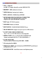
EX-9388L 386SX CPU CARD
386SX-40, 4MB, DOC SSD Socket, COM x 2,
IDE, RS-232x1 +RS232/422/485x1, WDT, I/O
PC/104, Single +5V
COPYRIGHT NOTICE
This user’s manual list necessary information to assist both Embedded
Computer manufacturers and end users in installing and setting up the
system. The information contained in this user’s manual is subject to
change without any notice.
This manual is copyrighted 2002. You may not reproduce by any way.
ACKNOWLEDGEMENTS
All trademarks and registered trademarks which mentioned in this
manual are the property belongs to their respective owners.
1
1
TABLE OF CONTENTS
CHAPTER 1: INTRODUCTION
1-1
1-2
1-3
ABOUT THIS MANUAL --------------------------------------------SPECIFICATION -----------------------------------------------------SAFETY PRECAUTIONS -------------------------------------------
5
6
7
CHAPTER 2: HARDWARE CONFIGURATION
2-1
2-2
2-3
2-4
2-5
2-6
2-7
2-8
2-9
2-10
2-11
2-12
2-13
2-14
2-15
2-16
2-17
2-18
2-19
2-20
2-21
2-22
2-23
JUMPER & CONNECTOR QUICK REFERENCE TABLE-COMPONENT LOCATIONS ---------------------------------------IDE CONNECTOR ---------------------------------------------------PRINTER CONNECTOR --------------------------------------------FLOPPY DISK DRIVE CONNECTOR ---------------------------JST 5-PIN KEYBOARD CONNECTOR ------------------------ISO 2-PIN POWER CONNECTOR ------------------------------COM1 RS-232 CONNECTOR -------------------------------------COM2 RS-232 CONNECTOR ------------------------------------RS-422/485 CONNECTOR -----------------------------------------JST 5-PIN PS/2 MOUSE CONNECTOR -----------------------VGA CONNECTOR --------------------------------------------------LCD CONNECTOR --------------------------------------------------CMOS BATTERY CLEAR JUMPER ----------------------------LCD PANEL VOLTAGE CONNECTOR ------------------------COM2 RS-232 OR RS-422/485 SELECT ---------------------M-System ADDRESS SELECT-----------------------------------POWER LED ---------------------------------------------------------HARD DISK ACTIVE LED -----------------------------------------SYSTEM RESET SWITCH -----------------------------------------BUZZER ----------------------------------------------------------------DOC SOCKET ---------------------------------------------------------MEMORY INSTALLATION -----------------------------------------
9
10
11
11
12
12
12
13
13
13
13
13
14
14
14
14
15
15
15
15
15
15
15
CHAPTER 3: M-SYSTEM DiskOnChip Flash Disk
3-1
3-2
3-3
PREFACE ---------------------------------------------------------------QUICK INSTALLATION GUIDE -----------------------------------UTILITY REFERENCE ------------------------------------------------
17
17
18
2
2
CHAPTER 4: WDT
4-1
4-2
WATCHDOG TIMER FUNCTION ---------------------------------WATCHDOG TIMER SOFTWARE GUIDE -----------------------
20
22
CHAPTER 5: VGA / LCD FLAT PANEL
5-1
5-2
5-3
5-4
FLAT PANEL BIOS SUPPORT
PANEL SWITCH UTILITY
FEATURE
SOFTWARE INSTALLING
24
25
26
26
CHAPTER 6: AWARD BIOS SETUP
6-1
6-2
6-3
6-4
6-5
6-6
6-7
6-8
6-9
6-10
INTRODUCTION -------------------------------------------------------STARTING SETUP ----------------------------------------------------MAIN MENU -------------------------------------------------------------STANDARD CMOS SETUP -----------------------------------------ADVANCED CMOS SETUP -----------------------------------------ADVANCED CHIPSET SETUP ------------------------------------PCI / PLUG AND PLAY SETUP --------------------------------PERIPHERAL SETUP -----------------------------------------------CHANGE SUPERVISOR PASSWORD --------------------------BIOS DEFAULT DRIVE TABLE ------------------------------------
28
28
29
31
34
37
40
42
45
46
APPENDIX A: EXPANSION BUS
A-1
A-2
PC/104 CONNECTOR PIN ASSIGNMENT ---------------------ISA BUS PIN ASSIGNMENT ----------------------------------------
49
50
APPENDIX B: TECHNICAL SUMMARY
B-1
B-2
B-3
B-4
INTERRUPT MAP ----------------------------------------------------RTC & CMOS RAM MAP -------------------------------------------TIMER & DMA CHANNELS MAP --------------------------------I/O & MEMORY MAP --------------------------------------------------
52
53
54
55
APPENDIX C: TROUBLE SHOOTING
C-1
C-2
C-3
TROUBLE SHOOTING POST MESSAGES -------------------TROUBLE SHOOTING POST BEEP ----------------------------TROUBLE SHOOTING POST CODE ----------------------------
57
57
61
3
3
CHAPTER
INTRODUCTION
THIS CHAPTER SHOWS THE INFORATIONS ABOUT THIS BOARD AND
ITS SPECIFICATIONS.
SECTIONS INCLUDE :
* ABOUT THIS MANUAL
* SPECIFICATIONS
* SAFETY PRECAUTIONS
4
4
1-1 ABOUT THIS MANUAL
Thank you for purchasing 386SX CPU Card, M-System DiskOnChip Flash
Disk ,fully DOS Command compatible. With full standard IPC functions
and other features, this 386SX CPU Card more suitable for harsh
industrial environment and commercial application. This manual is
written to assist you to install and set up the system. It contents five
chapters as following:
Chapter 1: Introduction
This chapter introduces you the background of this manual, and the
specification for this system. Final in this chapter will indicate you how
to avoid the damages for this Embedded CPU M-Card.
Chapter 2: Hardware Configuration
This chapter outlines the components’ locations and their functions.
In the end of this chapter, you will know how to set jumper and how
to configure this card to meet your own needs.
Chapter 3: M-System DiskOnChip Flash Disk
This chapter brings you the information about FLASH DISK function.
Chapter 4: WDT
Helpful information that informs you the proper installations of the
SSD and Flash BIOS, also describes the Watchdog-timer function.
Chapter 5: VGA / LCD FLAT PANEL
This chapter about VGA, TFT/DSTN/EL LCD flat panel.
Chapter 6: AMI BIOS Setup
This chapter indicates you how to set up the BIOS configurations.
Appendix A: Expansion Bus
This appendix introduces you the expansion bus for PC-104.
Appendix B: Technical Summary
This appendix gives you the information about the AMI BIOS
Identification Strings and Technical maps.
Appendix C: Trouble Shooting
This appendix outlines the errors and offers you the methods to
solve the problems.
5
5
1-2 SPECIFICATIONS
* CPU + Chipset:
ALI M6117C single chip with on-chip 386SX-40 CPU.
* MEMORY: 4MB soldered on board .
* CMOS Backup: backup by Li battery.
* BIOS: AMI BIOS, 128KB (Flash) EPROM.
* KEYBOARD AND PS/2 MOUSE CONNECTOR:
Support JST 5-pin PS/2 Keyboard Connector.
Support JST 5-pin PS/2 Mouse Connector.
* BUS Type: PC/104 Connector.
* SPEAKER: Buzzer on Board.
* WATCHDOG: 1/2/4/8/16/32/64/128/256/512 sec.
* IDE INTERFACE: Support one port up to 2 x IDE devices.
* FLOPPY DISK DRIVE INTERFACE:
Two 3 1/2” or 5 1/4” FDD, Drives A, B swappable.
* SERIAL PORT x 2: 2 x 16-byte FIFO 16C550 RS-232.
Jumper selectable RS-232 x 3 + RS-232/422/485 x 1.
* FLASH DISK SSD:
32-pin socket for DiskOnChip SSD 8MB ~ 288MB.
* I/O setup built in BIOS.
* PARALLEL PORT: One bi-directional SPP/EPP/ECP parallel port
configured as LPT 1,2,3.
* LED INDICATOR:
Hard Disk access and System power
6
6
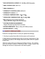
* BUS EXPANSION & SPEED: PC-104 8Mhz, BIOS Selectable
* DMA CONTROLLER: 82C37 X 2
* DMA CHANNELS: 7
* INTERRUPT CONTROLLERS: 82C59 X 2
* INTERRUPT LEVELS: 15
* STORAGE TEMPERATURE: -40℃ TO 80℃.
* OPERATING TEMPERATURE: 0℃ TO 60℃(140℉).
* Miscellaneous Connectors/Jumpers:
Reset, HDD LED, Single +5V 2-Pin connector.
* SYSTEM POWER REQUIREMENT:
Single +5V power by using 2-pin connector.
* BOARD DIMENSION: 95mm x 90mm PC/104 from factor.
* BOARD WEIGHT: 0.185Kg.
1-3 SAFETY PRECAUTIONS
Follow the messages below to avoid your system from damage.
1. Avoid your system from static electric power on all occasions.
2. Stay safe from the electric shock. Don’t touch any components of this
card when the power is ON. Always disconnect power when the system
is not in use.
3.Remove power when you change any hardware devices. For instance,
when you connect a jumper or install any cards, a surge of power may
damage the electronic components or the whole system.
7
7
CHAPTER
HARDWARE CONFIGURATION
THIS CHAPTER SHOWS YOU THE CONNECTORS & JUMPER SETTINGS,
AND COMPONENTS LOCATIONS.
SECTIONS INCLUDE:
* JUMPER/CONNECTOR QUICK REFERENCE TABLE
* COMPONENTS’ LOCATIONS
* CONFIGURATION AND JUMPER SETTINGS
* CONNECTOR PIN ASSIGNMENTS
8
8
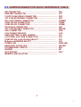
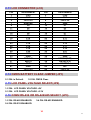
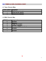
2-1 JUMPER/CONNECTOR QUICK REFERENCE TABLE
IDE CONNECTOR ……..…………….………………….…………
PRINTER CONNECTOR ...........................…..............…..…….
FLOPPY DISK DRIVE CONNECTOR ...................…………......
JST 5-PIN KEYBOARD CONNECTOR ……….…………………
ISO 2-PIN POWER CONNECTOR ………….……………………
COM1 RS-232 CONNECTOR ………………………..…………..
COM2 RS-232 CONNECTOR……………………………………..
RS-422/485 CONNECTOR ..…..………..………..…………..…..
JST 5-PIN MOUSE CONNECTOR ……..………………………..
VGA CONNECTOR ………………………………………………..
LCD CONNECTOR192D:
CMOS BATTERY CLEAR JUMPER ………..……………………
LCD PANEL VOLTAGE CONNECTOR ………………………….
COM2 RS-232 or RS-422/485 SELECT ………………………
M-System ADDRESS SELECT ..…………...……….…………...
POWER LED ………...……..…..……….…….…….……..………
HARD DISK ACTIVE LED ...……..……………..….……………..
SYSTEM RESET SWITCH ……….…..............…………………..
BUZZER …………………...…….…………………………………..
DOC SOCKET ……………………………….……………………..
MEMORY INSTALLATION ……………………………………….
IDE
LPT
FDC
K/B
POWER
COMA
COMB
CN1
MOUSE
VGA
LCD
JP1
JP2
JP3
JP4
PWR-LED
HD-LED
RST
BZ
DOC
9
9
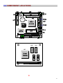
2-2 COMPONENT LOCATIONS
CN1
JP1
IDE
HD-LED
JP2
PWR-LED
RST
JP3
+
1
1
BZ
1
LPT
1
FDC
+ BAT
COMA
BAT
ALi
LCD
1
ALi M6117C
1
COMB
1
VGA
smsc
Mouse
DOC
FDC37C669
K/B
PC104
5V GND
1
POWER
JP4
U15
ALLIANCE
AS4C1M16E5-60
ALLIANCE
AS4C1M16E5-60
U17
U16
U19
TOPRO
ESMT
M11816161A-45J
ESMT
M11816161A-45J
TP6508IO
U18
10
10
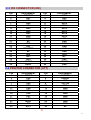
2-3 IDE CONNECTOR (IDE)
PIN
1
3
5
7
9
11
13
15
17
19
21
23
25
27
29
31
33
35
37
39
ASSIGNMENT
IDEREST
HD7
HD6
HD5
HD4
HD3
HD2
HD1
HD0
GND
NC
IOW
IOR
IOCHRDY
NC
IRQ
SA1
SA0
HDCS0
DASP
PIN
2
4
6
8
10
12
14
16
18
20
22
24
26
28
30
32
34
36
38
40
ASSIGNMENT
GND
HD8
HD9
HD10
HD11
HD12
HD13
HD14
HD15
NC
GND
GND
GND
ALE
GND
IO16
NC
SA2
HDCS1
GND
2-4 PRINTER CONNECTOR (LPT)
PIN
1
3
5
7
9
11
13
15
17
19
21
23
25
ASSIGNMENT
STROB
PD0
PD1
PD2
PD3
PD4
PD5
PD6
PD7
ACK
BUSY
PE
SLCT
PIN
2
4
6
8
10
12
14
16
18
20
22
24
26
ASSIGNMENT
AUTOFD
ERROR
INIT
SLCTIN
GND
GND
GND
GND
GND
GND
GND
GND
NC
11
11
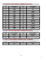
2-5 FLOPPY DISK DRIVE CONNECTOR (FDC)
PIN
1
3
5
7
9
11
13
15
17
19
21
23
25
27
29
31
33
ASSIGNMENT
GND
GND
GND
GND
GND
GND
GND
GND
GND
GND
GND
GND
GND
GND
GND
GND
GND
PIN
2
4
6
8
10
12
14
16
18
20
22
24
26
28
30
32
34
ASSIGNMENT
RPM
NC
NC
INDEX
MTR0
DRV1
DRV0
MTR1
DIR
STEP
WDATA
WGATE
TRK0
WRTPRT
RDATA
SEL
DSKCHG
2-6 JST 5-PIN KEYBOARD CONNECTOR (K/B)
PIN
1
3
5
ASSIGNMENT
KBCLK
NC
VCC
PIN
2
4
ASSIGNMENT
KBDATA
GND
2-7 ISO 2-PIN POWER CONNECTOR (POWER)
PIN
1
ASSIGNMENT
+5V
PIN
2
ASSIGNMENT
GND
12
12
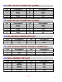
2-8 COM1 RS-232 CONNECTOR (COMA)
PIN
1
3
5
7
9
ASSIGNMENT
DCD1
RXD1
TXD1
DTR1
GND
PIN
2
4
6
8
ASSIGNMENT
DSR1
RTS1
CTS1
RI1
NC
2-9 COM2 RS-232 CONNECTOR (COMB)
PIN
1
3
5
7
9
ASSIGNMENT
DCD2
RXD2
TXD2
DTR2
GND
PIN
2
4
6
8
10
ASSIGNMENT
DSR2
RTS2
CTS2
RI2
NC
2-10 RS-422/485 CONNECTOR (CN1)
PIN
1
3
ASSIGNMENT
TX+
TX-
PIN
2
4
ASSIGNMENT
RXRX+-
2-11 JST 5-PIN PS/2 MOUSE CONNECTOR (MOUSE)
PIN
1
3
5
ASSIGNMENT
MCLK
NC
VCC
PIN
2
4
ASSIGNMENT
MDATA
GND
PIN
2
4
6
8
10
ASSIGNMENT
NC
NC
NC
GND
GND
2-12 VGA CONNECTOR (VGA)
PIN
1
3
5
7
9
ASSIGNMENT
RED
GREEN
BLUE
H-SYNC
V-SYNC
13
13
2-13 LCD CONNECTOR (LCD)
PIN
1
3
5
7
9
11
13
15
17
19
21
23
25
27
29
31
33
35
37
39
41
43
ASSIGNMENT
+12V
GND
+5V/3.3V
ENAVEE
P0
P2
P4
P6
P8
P10
P12
P14
P16
P18
P20
P22
GND
SHFCLK
M(D.0)
GND
GND
+5V/3.3V
PIN
2
4
6
8
10
12
14
16
18
20
22
24
26
28
30
32
34
36
38
40
42
44
ASSIGNMENT
+12V
GND
+5V/3.3V
GND
P1
P3
P5
P7
P9
P11
P13
P15
P17
P19
P21
P23
GND
VSYNC(FLM)
HSYNC(LP)
ENABLK
N/C
+5V/3.3V
2-14 CMOS BATTERY CLEAR JUMPER (JP1)
2-3 ON: is Default.
1-2 ON: CMOS Clear.
2-15 LCD PANEL VOLTAGE SELECT(JP2)
1-2 ON: LCD PANEL VOLTAGE +5V
2-3 ON: LCD PANEL VOLTAGE +3.3V
2-16 COM2 RS-232 OR RS-422/485 SELECT (JP3)
1-2 ON: RS-485 ENABLED.
5-6 ON: RS-232 ENABLED.
3-4 ON: RS-422 ENABLED.
14
14
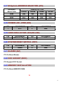
2-17 M-System ADDRESS SELECTOR (JP4)
ADDRESS
SELECTION
C000
C800
D000
D800
JUMPER SETTING
PIN3&4
PIN5&6
OFF
OFF
ON
OFF
OFF
ON
OFF
OFF
PIN1&2
ON
OFF
OFF
OFF
PIN7&8
OFF
OFF
OFF
ON
2-18 POWER LED (PWR-LED)
PIN
1
ASSIGNMENT
VCC
PIN
2
ASSIGNMENT
GND
2-19 HARD DISK ACTIVE LED (HD-LED)
PIN
1
ASSIGNMENT
HDD Active Signal
PIN
2
ASSIGNMENT
VCC
2-20 SYSTEM RESET SWITCH (RST)
PIN
1
ASSIGNMENT
Reset
PIN
2
ASSIGNMENT
GND
2-21 BUZZER (BZ)
IT’S On Board Buzzer.
2-22 DOC SOCKET (DOC)
IT’S Support DOC Socket.
2-23 MEMORY INSTALLATION
IT’S On Board 4MB EDO RAM.
15
15
CHAPTER
DiskOnChip FLASH DISK
THIS CHAPTER SHOWS
DiskOnChip FUNCTIONS.
THE
INFORMATION
ABOUT
M-System
SECTIONS INCLUDE:
* PREFACE
* QUICK INSTALLATION GUIDE
* UTILITY REFERENCE
16
16
3-1 PREFACE
This CPU Board features a DiskOnChip Flash Disk optional function. The
DiskOnChip can be build on board by order. This Board is designed to
use the DiskOnChip single chip Flash Disk to plug into a standard 32-pin
EEPROM socket which built on board. The DiskOnChip Flash Disk
should be mapped into an 8K Byte window in the BIOS expansion
address space of the CPU Card which is usually located between
address 0C000H to 0DFFFH. The CPU board can contain the operating
system in DiskOnChip to allow systems to boot without a hard disk.
The DiskOnChip of this board can install standard MS-DOS and the DOS
can boot from DiskOnChip, its command is fully DOS Command
compatible, such as Del, Deltree, Format, Copy, Xcopy, MD........, users
can read and write DOS Command or data to DiskOnChip same as when
using Hard Disk Drive.
Users can take this DiskOnChip as physical HDD and its priority is
software selectable. For example, if system have one HDD, either HDD &
DiskOnChip could be assigned as C or D Drive. When having two HDD
(Driver C & Driver D), the DiskOnChip could be assigned as C, D, E Drive.
If the system don’t have HDD, the DiskOnChip will be taken as C drive
only. When it is taken as C drive, it can boot system just same as using
Hard Disk Drive.
The capacity of DiskOnChip have 8MB, 12MB, 24MB, 40MB 72MB, 144MB
and 288MB option. User can select the proper one before order to meet
their needs.
This CPU Board support M-system DiskOnChip Socket which locate at
DOC.
3-2 QUICK INSTALLATION GUIDE
1.Make sure the CPU Card is power OFF
2.Plug the DiskOnChip chip into socket DOC. Verify the direction is
correct (pin1 of the DiskOnChip is aligned with pin1 of the DOC socket.
3.Power ON the system.
17
17
4.During power ON you may observe the message displayed by the
DiskOnChip when its driver automatically loaded into system’s
memory.
5.At this stage the DiskOnChip can be accessed as any disk in the
system.
6.If the DiskOnChip is the only disk in the system, it will appear as the
first disk (drive C).
7.If there are more disks besides the DiskOnChip, the DiskOnChip will
appear by default as the last drive.
3-3 UTILITY REFERENCE
A driver diskette will be included with DiskOnChip to offer detail
information. If you need more information beside the diskette, please
reach the M-System web www.m-sys.com to get the information.
18
18
CHAPTER
WDT
THIS CHAPTER SHOWS THE INFORMATION OF WDT FUNCTION, ALSO
DESCRIBES HOW TO INSTALL THE WATCHDOG CONFIGURATION.
SECTIONS INCLUDE:
* WATCHDOG TIMER FUNCTION
* WATCHDOG TIMER SOFTWARE GUIDE
Note: The M6117C has watchdog timer function for monitoring whether
The system is still work or not after a period of time. If the system
happened some error or hanged up, it cause the timer timed out,
then a system reset or NMI or IRQ may happen decided by BIOS
programming. The WATCHDOG timer source is 32.768 KHz
frequency to counter a 24 bits counter such that the timer range is
from 30.5 us to 512 sec with resolution 30.5 us.
19
19
4-1 WATCHDOG TIMER FUNCTION
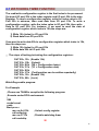
The read/write configuration register is the first index to be processed.
On board I/O port 22h is the index register and I/O port 23h is the data
Register. To read a configuration register, write the index value to I/O
Port 22h in advance, then read data from I/O port 23h. To write a
configuration register, write the index value to I/O port 22h, then write
Data to I/O port 23h. For instance, if we want to read the data of
configuration register which index is 10h,the steps are:
1) Write 10h (index) to I/O port 22h
2) Read data from I/O port 23h
If we want to write data 55h to configuration register which index is 12h,
then the steps are:
1) Write 12h (index) to I/O port 22h
2) Write data 55h to I/O port 23h
☆ The steps of locking/unlocking the configuration registers:
OUT 22h, 13h
OUT 23h, C5h
OUT 22h, XXh
OUT 23h, YYh
OUT 22h, XXh
OUT 23h, YYh
OUT 22h, 13h
OUT 23h, 00h
(Enable 13h)
(Unlock)
(XX = Configuration Index)
(YY = Configuration data)
(Configuration can be written repeatedly)
(Enable 13h)
(Lock)
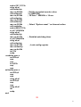
WatchDog enable program:
For Example
; Please use TASM to compiler the following program.
; Execute under DOS environment.
;
.286
.model smart
.code
Start proc c
mov ax,0c513h
; Unlock config register
call writechip
mov ax,3737h
; Disable watchdog timer
call readchip
20
20
and al,10111111b
xchg ah,al
call writechip
mov ax,083bh
call writechip
mov ax,003ah
call writechip
mov ax,0039h
call writechip
mov ax,3838h
call readchip
and al,00001111b
or al,11010000b
xchg ah,al
call writechip
mov ax,3737h
or al,01000000b
xchg ah,al
call writechip
mov ax,0013h
mov writechip
mov ax,4c00h
int 21h
endp
readchip proc c
out 22h,al
nop
nop
in al,23h
nop
nop
writechip proc c
out 22h,al
nop
nop
xchg ah,al
out 23h,al
nop
nop
xchg ah,al
ret
endp
end
; Set the expected counter value
; to [080000h]
; 30.5usc * 080000h = 16 sec
; Select “System reset “ as timeout action
; Enabled watchdog timer
; Lock config register
21
21
4-2 WATCHDOG SOFTWARE GUIDE
User can use WDT function by following way:
1.Direct start WDT function as procedure which described on Sec. 4-1.
2.Or, user can change WDT timing by choosing the items on WATCH
DOG TIMER in AMI BIOS ADVANCED CMOS SETUP.
If user control WDT by changing BIOS SETUP, application software must
note: one byte setup value was put on CMOS location 44H so application
software designer must read (access) the data on the CMOS location 44H and
put the data to a register then, at the time when you need, send the register
data to I/O port 0443H to start the WDT function.
Reset watchdog timer
Resets the watchdog timer periodically to prevent timeout.
mov ax,0c513h
; Unlock configuration register
call writechip
mov ax,3c3ch
; reset watchdog timer counter
call readchip
or al,00100000b
; The counter is reset at out 23h,al
xchg ah,al
call writechip
mov ax,0013h
; Lock configuration register
call writechip
(the above code uses reachip and writechip procedures)
22
22
CHAPTER
VGA / LCD FLAT PANEL
This section is can shows you the SVGA and LCD Flat Panel Video.
Sections include:
* FLAT PANEL BIOS SUPPORT
* PANEL SWITCHING UTILITY
* FEATURE
* SOFTWARE INSTALLING
23
23
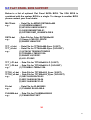
5-1 FLAT PANEL BIOS SUPPORT
Below is a list of optional Flat Panel SVGA BIOS. The VGA BIOS is
combined with the system BIOS in a single. To change to another BIOS
please contact your local dealer.
MLCD.dat
e.g. :
- Data File for MONO DSTN640x480
(1) HOSIDEN HLM6667
(2) HITACHI LMG5160XUFC
(3) CASIO MD650TS00-01
(4) OPTREX DMF_50260NFU-FW-8
DSTN.dat
e.g. :
- Data File for Color DSTN640x480
(1) Sanyo LCM-5331-22NTK
(2) SHARP LM64C35P
TFT_s1.dat
TFT_s2.dat
e.g. :
- Data File for TFT640x480-Sync (16 BIT)
- Data File for TFT640x480-Sync (18/24 BIT)
(1) HITACHI TX26D60/TX24D55
(2) TOSHIBA LTM09C015A
(3) SHARP LQ10D321
(4) LG LP104V2
TFT_LP1.dat - Data File for TFT640x480-LP (16 BIT)
TFT_LP2.dat - Data File for TFT640x480-LP (18/24 BIT)
e.g. :
(1) TOSHIBA LTM09c015A
TFT86_s1.dat - Data File for TFT800x600_Sync (16 BIT)
TFT86_s2.dat - Data File for TFT800x600_Sync (18/24 BIT)
e.g. :
(1) NEC NL8060AC26-05
(2) NEC NL8060AC26-04
(3) NEC NL8060BC31-02
EL.dat
e.g. :
- Data File for EL640X800
(1) PLANAR EL640.480-A
PLASMA.dat - Data File for PLASMA640X480
e.g. :
(1) PANASONIC S817
24
24
☆ Dual-scan STN Frame Buffer
Shadow Frame Buffer onto display memory for mono or color
LCD panel.
Pseudo Frame Buffer for color LCD panel (no additional DRAMs
required).
External Frame Buffer for color LCD panel (external additional
DRAMs required)
☆ Enhanced mode includes:
132 x 25 or 132 x 44 text mode
640 x 480/256 colors(Windows accelerations mode support optional)
640 x 480/65536 colors(Windows accelerations mode support optional)
640 x 480/16.8M colors(Windows accelerations mode support optional)
800 x 600/16
colors
800 x 600/256 colors(Windows accelerations mode support optional)
800 x 600/65536 colors(Windows accelerations mode support optional)
800 x 600/16.8M colors
1024 x 768/16 colors
1024 x 768/256 colors(Windows accelerations mode support optional)
1024 x 768/65536 colors(Windows accelerations mode support optional)
1280 x 1024/16 colors(Windows accelerations mode support optional)
1280 x 1024/256 colors(Windows accelerations mode support optional)
1600 x 1280/16 colors interlace display mode
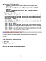
5-2 PANEL SWITCHING UTILITY
The Panel Switch Utility is used for switching different display type.
UASGE:
Type >SW508 then Screen will show
1. CRT Only
2. Panel Only
3. CRT/Panel Simultaneous
then you can choose which one you want to.
25
25
5-3 FEATURE
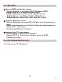
☆ Memory DRAM configuration support
Support symmetric or asymmetric RAS/CAS address DRAM
Support dual-CAS or dual-WE addressing DRAM
512k Bytes Memory: four 256k x 4-bit/ one 256k x 16- bit
1M Bytes Memory: eigh 256k x 4- bit/two 256k x 16-bit
2M Bytes Memory: sixteen 256k x 4-bit / four 256k x 16-bit
☆ Integrates STN panel support
Support Dual/single scan mono STN LCD Panel, up to 64 simultaneous
grays.
Support Dual/single scan color STN LCD Panel, up to 64k simultaneous
colors, and 61 visual color .
Provide 8 and 16 bit panel interfaces
☆Integrates color TFT panel support
Support Normal or CRT-like TFT LCD panel
Support 9/12/15 or 18/24 bit panel interface, and up to 16.8M
simultaneous colors.
5-4 SOFTWARE INSTALLING
1.You can see our CD “Readme.txt”
26
26
CHAPTER
AMI BIOS SETUP
THIS CHAPTER SHOWS HOW TO SET UP THE AMI BIOS.
SECTIONS INCLUDE:
* INTRODUCTION
* STARTING SETUP
* MAIN MENU
* STANDARD CMOS SETUP
* ADVANCED CMOS SETUP
* ADVANCED CHIPSET SETUP
* POWER MANAGEMENT SETUP
* PERIPHERAL SETUP
* CHANGE SUPERVISOR PASSWORD
* BIOS DEFAULT DRIVE TABLE
27
27
6-1 INTRODUCTION
This section discusses AMI Setup program built in the ROM BIOS. The Setup
program allows users to modify the basic system configuration. This special
information is then stored in battery-backed RAM so that it retains the Setup
information when the power is turned off.
The AMI BIOS installed in computer system’s ROM (Read Only Memory) is a
custom version of an industry standard BIOS. This means it supports
Intel/Cyrix/AMD processors in a standard IBM AT compatible Input/Output
system. The BIOS provides critical low-level support for standard devices
such as disk drives, serial and parallel ports. Also the BIOS has been
customized by adding important, but non-standard, features such as virus
and password protection as well as special support for detailed fine-tuning of
the chipset controlling the entire system. The rest of this chapter will try to
guide you the process of configuring your system by using Setup.
6-2 STARTING SETUP
The AMI BIOS is immediately activated when the computer starting power on.
The BIOS reads the system information contained in the CMOS and start the
process of checking out the system and configuring it. When it finish, the
BIOS will seek an operating system on one of the disks and then launch and
turn control over to the operating system.
While the BIOS is in active, the Setup program can be activated by one of two
ways:
1. Press the <Del> key immediately after switching the system on, or
2. Press the <Del> key when the following message appears briefly
at the bottom of the screen during the POST (Power On Self Test)
Press DEL to enter SETUP.
If the message disappears before you respond and you still wish to enter
Setup, restart the system to try again by turning it OFF then ON or pressing
the “RESET” bottom on the system case. You may also restart by
simultaneously pressing <Ctrl>, <Alt>, and <Delete> keys. If you do not
press the keys at the correct time and the system does not boot, an error
message will be displayed and you will again be asked to...
PRESS F1 TO CONTINUE, DEL TO ENTER SETUP
28
28
6-3 MAIN MENU
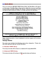
Once you enter the AMI BIOS CMOS Setup Utility, the Main Menu will appear
on the screen. The Main Menu allows you to select the one you need from
several setup functions and two exit choices. Use the arrow keys to select
among the items and press <Enter> to accept and enter the sub-menu.
AMIBIOS HIFLEX SETUP UTILITY - VERSION 1.23
( C ) 1999 American Megatrends, INC. All Rights RESERVED
Standard CMOS Setup
Advanced CMOS Setup
Advanced Chipset Setup
PCI / Plug and Play Setup
Peripheral Setup
Auto-Detect Hard Disks
Change User Password
Change Supervisor Password
Change Language Setting
Auto Configuration with Optimal Settings
Auto Configuration with Fail Safe Settings
Save Settings and Exit
Exit Without Saving
Standard CMOS setup for changing time, date, hard disk type, etc.
ESC:Exit ↑↓: Sel F2/F3: Color F10: Save & Exit
Note: a brief description of each highlighted selection appears at the bottom
of the screen.
Setup Items:
The main menu includes the following main setup categories. Please note
that some systems may not include all entries.
z Standard CMOS Setup
This setup includes all the items in a standard AT-compatible BIOS.
z Advanced CMOS Setup
This setup includes all the items of AMI special enhanced features.
29
29
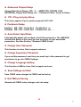
z Advanced Chipset Setup
Change Boot from (Floppy, IDE – 0…, ARMD-FDD, CDROM, SCSI,
NETWORK), Floppy Drive Swap, etc…, Password Check, or just to Setup.
z PCI / Plug and play Setup
This setup appears if your system supports PnP / ISA.
z Peripheral Setup
Enabled IDE , FDC , Serial Port , Parallel Port or
Disabled IDE , FDC , Serial Port , Parallel Port etc , …
z Auto-Detect Hard Disks
Automatically detect and configure hard disk parameters. The AMI BIOS
include this ability in the event you are uncertain of your hard disks’
parameters. See also Section “Standard CMOS Setup”.
z Change User Password
This function is close. Don’t support end-user.
z Change Supervisor Password
If you set this password, next time you must key in this password to get
permission to go into CMOS Settings .
z Change Language Setting
This function of AMI is close. Don’t support end-user.
z Save Settings and Exit
Save CMOS value changes to CMOS and exit setup
z Exit Without Saving
Abandon all CMOS value changes and exit setup.
30
30
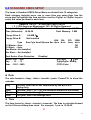
6-4 STANDARD CMOS SETUP
The items in Standard CMOS Setup Menu are divided into 10 categories.
Each category includes none, one or more than one setup item. Use the
arrow keys to highlight the item and then use the <PgUp> or <PgDn> keys to
select the value you want in each item.
AMIBIOS SETUP - STANDARD CMOS SETUP
( C ) 1999 American Megatrends, INC. All Rights Reserved
Date (mm/dd/yyyy):Wed Jan 09 , 2002
Base Memory: 640KB
Time (hh/mm/ss): 10:56:28
Extd Memory: 3 MB
Floppy Drive A:
Floppy Drive B:
1.44 MB 3½
Not Installed
LBA
Blk
Type
Size Cyln Head Wpcom Sec Mode Mode
Pri Master : Auto
Pri Slave : Auto
Sec.Master: Not Installed
Sec.Slave : Not Installed
Boot Sector Virus Protection
Month: Jan - Dec
Day : 01 - 31
Year : 1901 - 2099
PIO
32Bit
Mode
Mode
Off
Off
Disabled
ESC:Exit
↑↓:Sel
PgUp/PgDn: Modify
F2/F3:Color
z Date
The date format is <day>, <date> <month> <year>. Press<F3> to show the
calendar.
Day
Date
Month
Year
The day, from Sun to Sat, determined by the BIOS & is
display-only
The date, from 1 to 31 (or the maximum allowed in the month)
The month, Jan through Dec.
The year, from 1900 through 2099
z Time
The time format is <hour> <minute> <second>. The time is calculated based
on the 24-hour military-time clock. For example, 1 p.m. is 13:00:00.
31
31
z Daylight saving
The category adds one hour to the clock when daylight-saving time begins. It
also subtracts one hour when standard time returns.
Enabled
Disabled
Enable daylight saving
Disable daylight saving
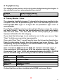
z Primary Master / Slave
The categories identify the types of 1 channels that have been installed in the
computer. There are 45 predefined types and 4 user definable types are for
Enhanced IDE BIOS. Type “1” to Type “45” are predefined. Type “user” is
user-definable.
Press PgUp or PgDn to select a numbered hard disk type or type the number
and press <Enter>. Note that the specifications of your drive must match
with the drive table. The hard disk will not work properly if you enter
improper information for this category.
If your hard disk drive type is not matched or not in list, you can use Type
“User” to define your own drive type manually.
If you select Type “User”, you will need to know the information listed below.
Enter the information directly from the keyboard and press <Enter>. This
information should be included in the documentation from your hard disk
vendor or the system manufacturer.
If the controller of HDD interface is ESDI, the selection should be “Type 1”.
If the controller of HDD interface is SCSI, the selection should be “None”.
If you select Type “Auto”, BIOS will automatically detect the HDD & CD-ROM
Drive at the POST stage and showing the IDE for HDD & CD-ROM Drive.
TYPE
CYLS.
HEADS
WPCOM
SECTORS
MODE
Drive type
Number of cylinders
Number of heads
Write precom
Number of sectors
Mode type
If a hard disk has not been installed select NONE and press <Enter>.
32
32
z Drive A Type / Drive B Type
The category identifies the types of Floppy Disk Drive A or Drive B that have
been installed in the computer.
None
No floppy drive installed.
360K, 5.25 in 5¼” PC-type standard drive; 360K byte capacity.
1.2M, 5.25 in 5¼” AT-type high-density drive; 1. 2M byte capacity.
720K, 3.5 in 3½” double-sided drive; 720K byte capacity.
1.44M, 3.5 in 3½” double-sided drive; 1. 44M byte capacity.
2.88M, 3.5 in 3½” double-sided drive; 2.88M byte capacity.
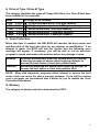
z Virus Protection
When this item is enabled, the AMI BIOS will monitor the boot sector and
partition table of the hard disk drive for any attempt on modification. If an
attempt is made, the BIOS will halt the system and the following error
message will appear. If necessary, you will be able to run an anti-virus
program to locate and remove the problem before any damage is done.
Enabled
Disabled
Activates automatically when the system boots up causing
a warning message to appear when anything attempts to
access the boot sector or hard disk partition table.
No warning message will appear when anything attempts to
Access the boot sector or hard disk partition table.
NOTE: Many disk diagnostic programs which attempt to access the boot
sector table can cause the above warning message. If you will be running
such a program, we recommend that it better for you to disable the Virus
Protection beforehand.
z Memory
The category is display-only item determined by POST.
33
33
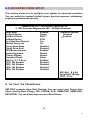
6-5 ADVANCED CMOS SETUP
This section allows you to configure your system for advanced operation.
You can select the system’s default speed, boot-up sequence, shadowing,
keyboard operation and security.
AMIBIOS SETUP – ADVANCED CMOS SETUP
© 1999 American Megatrends, INC . All Right Reserved
Quick Boot
1st Boot Device
2nd Boot Device
3rd Boot Device
Try Other Boot Devices
BootUp Num-Lock
Floppy Drive Swap
Floppy Drive Seek
PS/2 Mouse Support
System Keyboard
Primary Display
Password Check
Wait For ‘F1’ If Error
C000, 32k Shadow
C800, 32k Shadow
D000, 32k Shadow
D800, 32k Shadow
Enabled
Floppy
IDE-0
SCSI
Yes
On
Disabled
Disabled
Enabled
Absent
Absent
Setup
Enabled
Disabled
Disabled
Disabled
Disabled
Available Options
Disabled
Enabled
ESC:Exit ↑↓:Sel
PgUp/PgDn :Modify
F2/F3 : Color
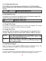
z 1st (2nd , 3rd ) Boot Device
AMI BIOS supports three Boot Devices. You can select your Device from
where starting Boot (Floppy, IDE, CDROM, SCSI, ARMD-FDD, ARMD-HDD,
NETWORK). You can select anyone to be a Boot Device.
34
34
z Try Other Boot Devices
If Yes, BIOS will try to boot from other Boot Devices if all Selected Boot
Devices failed to boot. If NO, BIOS will try to Boot from only the Selected Boot
Devices.
YES
NO
Enabled Another Boot Device
Disabled Another Boot Device
z BootUp Num-Lock
This allows you to determine the default status of the numeric keypad. By
default, the system boots up with NumLock on.
ON
OFF
Keypad is number keys
Keypad is arrow keys
z Floppy Drive Swap
Set this option to Enabled to permit drives A: and B: to be swapped. The settings
are Enabled or Disabled. The default settings are Disabled.
z Floppy Drive Seek
During POST, BIOS will determine if the floppy disk drive installed is 40 or
80 tracks. 360K type is 40 tracks while 760K, 1.2M and 1.44M are 80 tracks.
Enabled
Disabled
BIOS searches for floppy disk drive to determine if it is 40 or 80
tracks. Note that BIOS can not tell from 720K, 1.2M or 1.44M
drive type as they are all 80 tracks.
BIOS will not search for the type of floppy disk drive by track
number. Note that there will not be any warning message if the
drive installed is 360K.
z PS/2 Mouse Support
When this option is set to Enabled, AMIBIOS supports a PS/2-type mouse. The
settings are Enabled or Disabled. The default settings are Disabled.
z System Keyboard
This option specifies that a keyboard is attached to the computer. The settings are
Present or Absent. The Optimal and Fail-Safe default settings are Present
35
35
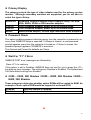
z Primary Display
The category selects the type of video adapter used for the primary system
monitor. Although secondary monitors are supported, you do not have to
select the type in Setup.
EGA/VGA
CGA 40
CGA 80
MONO
Enhanced Graphics Adapter/Video Graphics Array. For EGA,
VGA, SEGA, SVGA or PGA monitor adapters.
Color Graphics Adapter, power up in 40 column mode.
Color Graphics Adapter, power up in 80 column mode.
Monochrome adapter, include high-resolution mono adapters.
z Password Check
This option enables password checking every time the computer is powered on or
every time WINBIOS Setup is executed. If Always is chosen, a user password
prompt appears every time the computer is turned on. If Setup is chosen, the
password prompt appears if WINBIOS is executed.
The Optimal and Power-On defaults are Setup.
z Wait For “F1” if Error
AMIBIOS POST error messages are followed by:
Press <F1> to continue
If this option is set to Disabled, AMIBIOS does not wait for you to press the <F1>
key after an error message. The settings are Disabled or Enabled. The Optimal and
Fail-Safe default settings are Enabled
z C000 – C800, 32K Shadow / D000 – D800, 32K Shadow / E000 –
E800, 32K Shadow
These categories determine whether option ROMs will be copied to RAM. An
example of such option ROM would be support of on-board SCSI.
Enabled
Disabled
Optional shadow is enabled
Optional shadow is disabled
36
36
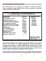
6-6 ADVANCED CHIPSET SETUP
This section allows you to configure your system for advanced operation.
You can select the system’s default speed, boot-up sequence, shadowing,
keyboard operation and security.
AMIBIOS SETUP – ADVANCED CMOS SETUP
© 1999 American Megatrends, INC. All Right Reserved
AT Bus Clock
Slow Refresh
Memory Hole At 15-16M
RAS Precharge time
RAS Active Time Insert Wait
CAS Precharge Time Insert Wait
Memory Write Insert Wait
Memory Miss Read Insert Wait
ISA Write cycle end Insert Wait
I/O Recovery
I/O Recovery Period
On – Chip I/O Recovery
16Bit ISA Insert Wait
WatchDog Timer
WatchDog Timeout Select
WatchDog Signal Select
14.318/2
15 us
Disabled
1.5T
Disable
Disable
Disable
Disable
Enabled
Enabled
0.75 us
Disable
Enabled
Disabled
1 Sec.
System
Available Options
14.318/2
PCLK2/3
PCLK2/4
PCLK2/5
PCLK2/6
PCLK2/8
PCLK2/10
PCLK2/12
ESC:Exit ↑↓:Sel
PgUp/PgDn :Modify
F2/F3 : Color
This section allows you to configure the system based on the specific
features of the chipset. The chipset manages bus speeds and access to
system memory resources, such as DRAM and the external cache. It also
coordinates the function of WDT timer. Please note that these items
shouldn’t need to be altered. The default settings have been chosen because
they provide the best operating conditions for your system.
The only time you might consider making any changes on this Setup would
be the time when you find that data was being lost while using your system.
37
37
z AT BUS Clock
ISA Bus Clock timing selection. When Auto Configuration is Disabled, then
14.318/2, PCLK2/3, PCLK2/4, PCLK2/5, PCLK2/6, PCLK2/8, PCLK2/10,
PCLK2/12 is available on ISA Bus.
z Slow Refresh
The chipset refresh settings deal with the timing of CPU access to dynamic
random access memory (DRAM). The default timing have been carefully
chosen and should only be altered if data is being lost. Such a scenario might
occur if your system had mixed speed DRAM chips installed so that treater
delays may be required to preserve the integrity of the data held in the slower
memory chips. Available values: 120us, 60us, 15us.
z Memory Hole At 15-16M
Use this option to specify an area in memory that cannot be addressed on the ISA
bus. The settings are Disabled, 512-640K, or 15-16MB. The default setting is
Disabled.
z RAS Precharge time
DRAM must continually be refreshed otherwise it will lose its data. Normally,
DRAM is refreshed entirely as the result of a single request. This option
allows you to determine the number of CPU clocks allocated for the Row
Address Strobe to accumulate its charge before the DRAM is refreshed. If
insufficient time is allowed, refresh may be incomplete and data will lose.
Available values: 3.5T, 2.5T, 1.5T.
z RAS Active Time Insert Wait
When it is Enabled, system will insert wait state for lower speed DRAM.
z CAS Precharge Time Insert Wait
z Memory Writer Insert Wait
z Memory Miss Read Insert Wait
Above three items show above is always Disabled by Manufactory’s default
z I/O Recovery
This item allows you to determine the recovery time allowed for 8 bit I/O.
Choices are 0u, 0.25u to 3.05 CPU clocks. Default is 1 clock.
38
38
z I/O Recovery Period
The recovery time is the length of time, measured in CPU clocks, which the
system will delay after the completion of an input/output request. This delay
takes place because the CPU is operating so much faster than the
input/output bus that the CPU must be delay to allow of the completion of the
I/O.
z WatchDog Timer
WatchDog can use BIOS Setup.
Disabled
Enabled
WatchDog can used.
WatchDog function Enabled.
z WatchDog Timeout Select
Set Timer 1, 2, 4, 8, 16, 32, 64, 128, 256, 512 sec
z WatchDog Signal Select
Set IRQ3, 4, 5, 6, 7, 9, 10, 11, 12, 14, 15, NMI, System.
39
39
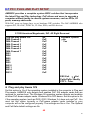
6-7 PCI / PLUG AND PLAY SETUP
AMIBIOS provides a complete system BIOS solution that incorporates
the latest Plug and Play technology. PnP allows end users to upgrade a
computer without having to choose system resources, such as IRQs, I/O
ports, memory addresses.
With PnP, users no longer have to set hardware DIP switches. The PnP AMIBIOS also
supports PCI, ISA PnP, PCMCIA, VL-Bus, EISA, and ISA devices.
AMIBIOS SETUP – PCI / PLUG AND PLAY SETUP
© 1999 American Megatrends, INC. All Right Reserved
Plug and play Aware O/S
DMA Channel 0
DMA Channel 1
DMA Channel 3
DMA Channel 5
DMA Channel 6
DMA Channel 7
IRQ3
IRQ4
IRQ5
IRQ7
IRQ9
IRQ10
IRQ11
IRQ14
IRQ15
No
PnP
PnP
PnP
PnP
PnP
PnP
PnP
PnP
PnP
PnP
PnP
PnP
PnP
PnP
PnP
Available Options
No
Yes
ESC:Exit ↑↓:Sel
PgUp/PgDn :Modify
F2/F3 : Color
z Plug and play Aware O/S
Set this option to Yes if the operating system installed in the computer is Plug and
Play-aware. AMIBIOS only detects and enables PnP ISA adapter cards that are
required for system boot. The Windows 95 operating system detects and enables
all other PnP-aware adapter cards. Windows 95 is PnP-aware. Set this option to No
if the operating system (such as DOS, OS/2, Windows 3.x) does not use PnP. You
must set this option correctly or PnP-aware adapter cards installed in your
computer will not be configured properly. The settings are No or Yes. The Optimal
and Fail-Safe default settings are No
40
40
z IRQ-XX assigned to
If your ISA card is not PnP compatible and requires a special IRQ to
support its function, set the select IRQ-x assigned to : “ISA”. This
setting informs the PnP BIOS to reserve the selected IRQ for the installed
legacy ISA card.
z DMA-X assigned to
If your ISA card is not PnP compatible and requires a special DMA
channel to support its function, set the select DMA channel to : “
ISA”. This setting informs the PnP BIOS to reserve the selected DMA
channel for the installed legacy ISA card
41
41
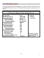
6-8 PERIPHERAL SETUP
Peripheral Setup options are displayed by choosing the Peripheral Setup icon from
the WINBIOS Setup main menu. All Peripheral Setup options are described in this
section.
AMIBIOS SETUP – PERIPHERAL SETUP
© 1999 American Megatrends, INC. All Right Reserved
Onboard IDE
Onboard FDD
Onboard Serial Port1
Onboard Serial Port2
Serial Port2 Mode
Receiver Polarity
Transmitter Polarity
Onboard Serial Port3
Serial Port3 IRQ
Onboard Serial Port4
Serial Port4 Mode
Serial Port4 IRQ
Receiver Polarity
Transmitter Polarity
Onboard Parallel Port
Parallel Port Mode
EPP Version
Parallel Port IRQ
Parallel Port DMA Channel
Onboard Parallel Port2
Primary
Auto
3F8h/COM1
2F8h/COM2
Normal
Non-Inverted
Non-Inverted
Disabled
N/A
N/A
N/A
N/A
N/A
N/A
378
ECP
N/A
5
3
Disabled
Available Options
Disable
Primary
Secondary
ESC:Exit ↑↓:Sel
PgUp/PgDn :Modify
F2/F3 : Color
42
42
z Onboard IDE
This option specifies the onboard IDE controller channels that will be used. The
settings are Primary, Secondary, Both, or Disabled. The Optimal and Fail-Safe
default settings are Primary
z Onboard FDD
This option enables the floppy drive controller on the motherboard. The settings are
Enabled or Disabled. The Optimal default setting is Enabled. The Fail-Safe default
setting is Disabled.
z Onboard Serial Port1
This option enables serial port 1 on the motherboard and specifies the base I/O port
address for serial port 1.
The settings are 3F8h, 3E8h, or Disabled. The Optimal default setting is 3F8h. The
Fail-Safe default setting is Disabled.
z Onboard Serial Port2
This option enables serial port 2 on the motherboard and specifies the base I/O port
address for serial port 2.
The settings are 2F8h, 2E8h, or Disabled. The Optimal default setting is 3F8h. The
Fail-Safe default setting is Disabled.
z Onboard Parallel Port
This option enables the parallel port on the motherboard and specifies the parallel
port base I/O port address. The settings are 378h, 278h, or Disabled.
The Optimal default setting is 378h. The Fail-Safe default setting is Disabled
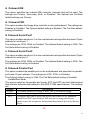
Parallel Port Mode
This option specifies the parallel port mode. ECP and EPP are both bidirectional
data transfer schemes that adhere to the IEEE P1284 specifications. The settings
are
Setting
Description
Normal The normal parallel port mode is used. This is the default setting.
Bi-Dir
Use this setting to support bidirectional transfers on the parallel port.
EPP
The parallel port can be used with devices that adhere to the Enhanced
Parallel Port (EPP) specification. EPP uses the existing parallel port
signals to provide asymmetric bidirectional data transfer driven by the host
device.
43
43
ECP
The parallel port can be used with devices that adhere to the Extended
Capabilities Port (ECP) specification. ECP uses the DMA protocol to
achieve transfer rates of approximately 2.5 Mbs. ECP provides symmetric
bidirectional communications.
Parallel Port DMA
This option is only available if the setting for the Parallel Port Mode option is ECP.
The settings are Disabled, DMA CH (channel) 0, DMA CH 1, or DMA CH 3. The default
setting is Disabled.
44
44
6-9 CHANGE SUPERVISOR PASSWORD
You can set either supervisor or user password, or both of them. The
difference between them are: ‘supervisor password’ can enter and change
the options of the setup menus and ‘user password’ just can enter but do not
have the right to change the options of the setup menus.
When you select this function, the following message will appear at the
center of the screen to assist you in creating a password.
ENTER PASSWORD:
Type the password, up to eight characters in length, and press <Enter>. The
password typed now will clear any previously entered password from CMOS
memory. You will be asked to confirm the password. Type the password
again and press <Enter>. You may also press <Esc> to abort the selection
and not enter a password.
To disable a password, just press <Enter> when you are prompted to enter
the password. A message will confirm the password will be disabled. Once
the password is disabled, the system will boot and you can enter Setup
freely.
PASSWORD DISABLED.
When a password has been enabled, you will be prompted to enter it every
time you try to enter Setup. This prevents an unauthorized person from
changing any part of your system configuration.
Additionally, when a password is enabled, you can also require the BIOS to
request a password every time your system is rebooted. This would prevent
unauthorized use of your computer.
You determine when the password is required within the BIOS Features
Setup Menu and its Security option. If the Security option is set to “System”,
the password will be required both at boot and at entry to Setup. If set to
“Setup”, prompting only occurs when trying to enter the Setup.
45
45
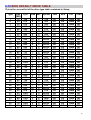
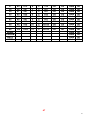
6-10 BIOS DEFAULT DRIVE TABLE
This is the current list of the drive type table contained in Setup.
Type
1
2
3
4
5
6
7
8
9
10
11
12
13
14
16
17
18
19
20
21
22
23
24
25
26
27
28
29
30
31
32
33
34
35
36
Size
(MB)
10
20
30
62
46
20
30
30
112
20
35
49
20
42
20
40
56
59
30
42
30
10
53
69
43
68
40
68
53
93
127
42
10
76
68
Cyln
306
615
615
940
940
615
462
733
900
820
855
855
306
733
612
977
977
1024
733
733
733
306
925
925
754
754
699
823
918
1024
1024
1024
612
1024
1024
Head Sec Wpcom
4
4
6
8
6
4
8
5
15
3
5
7
8
7
4
5
7
7
5
7
5
4
5
9
7
11
7
10
7
11
15
5
2
9
8
17
17
17
17
17
17
17
17
17
17
17
17
17
17
17
17
17
17
17
17
17
17
17
17
17
17
17
17
17
17
17
17
17
17
17
128
300
300
512
512
65535
256
65535
65535
65535
65535
65535
128
65535
300
300
65535
512
300
300
65535
65535
754
65535
256
65535
918
65535
65535
1024
128
65535
512
LBA
BLK
PIO
32BIT
Off
Off
Off
Off
Off
Off
Off
Off
Off
Off
Off
Off
Off
Off
Off
Off
Off
Off
Off
Off
Off
Off
Off
Off
Off
Off
Off
Off
Off
Off
Off
Off
Off
Off
Off
Off
Off
Off
Off
Off
Off
Off
Off
Off
Off
Off
Off
Off
Off
Off
Off
Off
Off
Off
Off
Off
Off
Off
Off
Off
Off
Off
Off
Off
Off
Off
Off
Off
Off
Off
Auto
Auto
Auto
Auto
Auto
Auto
Auto
Auto
Auto
Auto
Auto
Auto
Auto
Auto
Auto
Auto
Auto
Auto
Auto
Auto
Auto
Auto
Auto
Auto
Auto
Auto
Auto
Auto
Auto
Auto
Auto
Auto
Auto
Auto
Auto
Off
Off
Off
Off
Off
Off
Off
Off
Off
Off
Off
Off
Off
Off
Off
Off
Off
Off
Off
Off
Off
Off
Off
Off
Off
Off
Off
Off
Off
Off
Off
Off
Off
Off
Off
46
37
38
39
40
41
42
43
44
45
46
ARMD
CDROM
AUTO
USER
40
24
57
40
40
40
48
68
144
152
615
987
987
820
977
981
830
830
917
1224
8
3
7
6
5
5
7
10
15
15
17
17
17
17
17
17
17
17
17
17
128
987
987
820
977
981
512
65535
65535
65535
Off
Off
Off
Off
Off
Off
Off
Off
Off
Off
Off
Off
Off
Off
Off
Off
Off
Off
Off
Off
Auto
Auto
Auto
Auto
Auto
Auto
Auto
Auto
Auto
Auto
Auto
Auto
Auto
Auto
Off
Off
Off
Off
Off
Off
Off
Off
Off
Off
Off
Off
Off
Off
47
47
APPENDIX
EXPANSION BUS
THIS APPENDIX SHOWS YOU THE PIN ASSIGNMENTS.
SECTIONS INCLUDE:
* PC/104 CONNECTOR PIN ASSIGNMENT
* ISA BUS PIN ASSIGNMENT
48
48
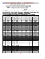
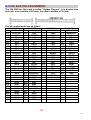
A-1 PC/104 CONNECTOR PIN ASSIGNMENT (P1)
104AB, 104CD : PC/104 Connector
The PC/104 can support multi-pieces of PC/104 modules. This card has
two connectors : one (104AB) consists of 64-pin dual-in-line header, the
other one (104CD) consists of 40-pin dual-in-line header
The pin assignments for connector 104AB & 104CD are as follow:
PIN
A1
A2
A3
A4
A5
A6
A7
A8
A9
A10
A11
A12
A13
A14
A15
A16
A17
A18
A19
A20
A21
A22
A23
A24
A25
A26
A27
A28
A29
A30
A31
A32
104AB
104CD
ASSIGNMENT PIN ASSIGNMENT PIN ASSIGNMENT PIN ASSIGNMENT
IOCHK
B1
GND
C1
GND
D1
GND
SD7
B2
RESETDRV
C2
SBHE
D2
MEMCS16
SD6
B3
VCC
C3
LA23
D3
IOCS16
SD5
B4
IRQ9
C4
LA22
D4
IRQ10
SD4
B5
-5V
C5
LA21
D5
IRQ11
SD3
B6
DRQ2
C6
LA20
D6
IRQ12
SD2
B7
-12V
C7
LA19
D7
IRQ15
SD1
B8
0WS
C8
LA18
D8
IRQ14
SD0
B9
+12V
C9
LA17
D9
DACK0
IOCHRDY
B10
GND
C10
MEMR
D10
DRQ0
AEN
B11
SMEMW
C11
MEMW
D11
DACK5
SA19
B12
SMEMR
C12
SD8
D12
DRQ5
SA18
B13
IOW
C13
SD9
D13
DACK6
SA17
B14
IOR
C14
SD10
D14
DRQ6
SA16
B15
DACK3
C15
SD11
D15
DACK7
SA15
B16
DRQ3
C16
SD12
D16
DRQ7
SA14
B17
DACK1
C17
SD13
D17
VCC
SA13
B18
DRQ1
C18
SD14
D18
MASTER
SA12
B19
REFRESH
C19
SD15
D19
GND
SA11
B20
SYSCLK
C20
KEY PIN
D20
GND
SA10
B21
IRQ7
SA09
B22
IRQ6
SA08
B23
IRQ5
SA07
B24
IRQ4
SA06
B25
IRQ3
SA05
B26
DACK2
SA04
B27
TC
SA03
B28
BALE
SA02
B29
VCC
SA01
B30
OSC
SA0
B31
GND
GA0
B32
GND
49
49
A-2 ISA BUS PIN ASSIGNMENT
The ISA BUS for this card is called “Golden Fingers”. It is divided into
two sets: one consists of 62 pins; the other consists of 36 pins.
The pin assignments are as follow :
PIN
A1
A2
A3
A4
A5
A6
A7
A8
A9
A10
A11
A12
A13
A14
A15
A16
A17
A18
A19
A20
A21
A22
A23
A24
A25
A26
A27
A28
A29
A30
A31
ISA BUSA
ASSIGNMENT
IOCHCHK*
SD7
SD6
SD5
SD4
SD3
SD2
SD1
SD0
IOCHRDY*
AEN
SA19
SA18
SA17
SA16
SA15
SA14
SA13
SA12
SA11
SA10
SA09
SA08
SA07
SA06
SA05
SA04
SA03
SA02
SA01
SA0
PIN
B1
B2
B3
B4
B5
B6
B7
B8
B9
B10
B11
B12
B13
B14
B15
B16
B17
B18
B19
B20
B21
B22
B23
B24
B25
B26
B27
B28
B29
B30
B31
ISA BUSB
ASSIGNMENT
GND
RESET
VCC
IRQ9
-5V
DRQ2
-12V
0WS
+12V
GND
SMEMW*
SMEMR*
IOW*
IOR*
DACK3
DRQ3
DACK1
DRQ1
REFRESH*
SYSCLK
IRQ7
IRQ6
IRQ5
IRQ4
IRQ3
DACK2
TC
BALE
VCC
OSC
GND
PIN
C1
C2
C3
C4
C5
C6
C7
C8
C9
C10
C11
C12
C13
C14
C15
C16
C17
C18
C19
C20
ISA BUSC
ASSIGNMENT
SBHE
LA23
LA22
LA21
LA20
LA19
LA18
LA17
MEMR*
MEMW*
SD8
SD9
SD10
SD11
SD12
SD13
SD14
SD15
SD15
KEY PIN
ISA BUSD
PIN ASSIGNMENT
D1
MEMCS16*
D2
IOCS16*
D3
IRQ10
D4
IRQ11
D5
IRQ12
D6
IRQ15
D7
IRQ14
D8
DACK0
D9
DRQ0
D10
DACK5
D11
DRQ5
D12
DACK6
D13
DRQ6
D14
DACK7
D15
DRQ7
D16
VCC
D17
MASTER*
D18
GND
D19
GND
D20
GND
50
50
APPENDIX
TECHNICAL SUMMARY
THIS SECTION SHOWS YOU THE MAPS CONCISELY.
SECTIONS INCLUDE:
* INTERRUPT MAP
* RTC & CMOS RAM MAP
* TIMER & DMA CHANNELS MAP
* I/O & MEMORY MAP
51
51
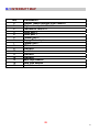
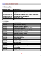
B-1 INTERRUPT MAP
IRQ
0
1
2
3
4
5
6
7
8
9
10
11
12
13
14
15
ASSIGNMENT
System TIMER interrupt from TIMER-0
Keyboard output buffer full
Cascade for IRQ 8-15
Serial port 2
Serial port 1
Parallel port 2
Floppy Disk adapter
Parallel port 1
RTC clock
Available
Available
Available
Available
Math coprocessor
Hard Disk adapter
Available
52
52
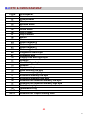
B-2 RTC & CMOS RAM MAP
CODE
00
01
02
03
04
05
06
07
08
09
0A
0B
0C
0D
0E
0F
10
11
12
13
14
15
16
17
18
30
31
32
33
34-3F
40-7F
ASSIGNMENT
Seconds
Second alarm
Minutes
Minutes alarm
Hours
Hours alarm
Day of week
Day of month
Month
Year
Status register A
Status register B
Status register C
Status register D
Diagnostic status byte
Shutdown byte
Floppy Disk drive type byte
Reserve
Hard Disk type byte
Reserve
Equipment byte
Base memory low byte
Base memory high byte
Extension memory low byte
Extension memory high byte
Reserved for extension memory low byte
Reserved for extension memory high byte
Date Century byte
Information Flag
Reserve
Reserved for Chipset Setting Data
53
53
B-3 TIMER & DMA CHANNELS MAP
z Timer Channel Map
Timer Channel Assignment
0
System timer interrupt
1
DRAM Refresh request
2
Speaker tone generator
z DMA Channel Map
DMA Channel Assignment
0
Available
1
IBM SDLC
2
Floppy Disk adapter
3
Channel-3 Available
4
Cascade for DMA controller 1
5
Available
6
Available
7
Available
54
54
B-4 I/O & MEMORY MAP
z Memory Map
MEMORY MAP
0000000-009FFFF
00A0000-00BFFFF
00C0000-00DFFFF
ASSIGNMENT
System memory used by DOS and application
Display buffer memory for VGA/EGA/CGA/MONO
adapter
Reserved for I/O device BIOS ROM or RAM buffer.
00E0000-00EFFFF
00F0000-00FFFFF
0100000-BFFFFF
Reserved for PCI device ROM
System BIOS ROM
System extension memory
z I/O Map
I/O MAP
000-01F
020-021
022-023
040-05F
060-06F
070-07F
080-09F
0A0-0BF
0C0-0DF
0F0-0FF
1F0-1F8
278-27F
2B0-2DF
2F8-2FF
360-36F
378-37F
3B0-3BF
3C0-3CF
3D0-3DF
3F0-3F7
3F8-3FF
ASSIGNMENT
DMA controller (Master)
Interrupt controller (Master)
Chipset controller registers I/O ports.
Timer control registers.
Keyboard interface controller (8042)
RTC ports & CMOS I/O ports
DMA register
Interrupt controller (Slave)
DMA controller (Slave)
Math coprocessor
Hard Disk controller
Parallel port-2
Graphics adapter controller
Serial port-2
Net work ports
Parallel port-1
Monochrome & Printer adapter
EGA adapter
CGA adapter
Floppy disk controller
Serial port-1
55
55
APPENDIX
TROUBLE
SHOOTING
THIS SECTION SHOWS THE ERRORS MAY OCCUR WHEN YOU OPERATE
THE SYSTEM, ALSO GIVES YOU THE SUGGESTIONS ON SOLVING THE
PROBLEMS.
SECTIONS INCLUDE:
* TROUBLE SHOOTING POST MESSAGE
* TROUBLE SHOOTING POST BEEP
* TROUBLE SHOOTING POST CODE
56
56
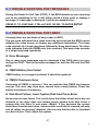
C-1 TROUBLE SHOOTING POST MESSAGES
During the Power On Self Test (POST), if the BIOS detects an error requiring
you to do something to fix, it will either sound a beep code or display a
message. If a message is displayed, it will be accompanied by:
PRESS F1 TO CONTINUE, CTRL-ALT-ESC OR DEL TO ENTER SETUP
C-2 TROUBLE SHOOTING POST BEEP
Currently there are two kinds of beep codes in BIOS.
The one code indicates that a video error has occurred and the BIOS cannot
initialize the video screen to display any additional information. This beep
code consists of a single long beep followed by three short beeps. The other
code indicates that your DRAM error has occurred. This beep code consists
of a single long beep repeatedly.
z Error Messages
One or more error messages may be displayed if the BIOS detect an error
during the POST. This list includes messages for both the ISA and the EISA
BIOS.
z CMOS Battery Has Failed
CMOS battery is no longer functional. It should be replaced.
z CMOS Checksum Error
Checksum of CMOS is incorrect. This can indicate that CMOS has become
corrupt. This error may have been caused from a weak battery. Check the
battery and replace if necessary.
z Disk Boot Failure, Insert System Disk And Press Enter
No boot device was found. This could mean that either a boot drive was not
detected or the drive does not contain proper system boot files. Insert a
system disk into Drive A: and press <Enter>. If you assumed the system
would boot from the hard drive, make sure the controller is inserted correctly
and all cables are properly attached. Also be sure that the disk is formatted
as a boot device. Then reboot the system.
57
57
z Diskette Drives Or Types Mismatch Error - Run Setup
Type of diskette drive installed in the system is different from the CMOS
definition. Run Setup to reconfigure the drive type correctly.
z Display Switch Is Set Incorrectly
Display switch on the motherboard can be set to either monochrome or color.
This indicates the switch is set to a different setting than indicated in Setup.
Determine which setting is correct, and then turn OFF the selection.
z Display Type Has Changed Since Last Boot
Since last power off the system, the display adapter has been changed. You
must configure the system for the new display type.
z Error Encountered Initializing Hard Drive
Hard drive cannot be initialized. Be sure the adapter is installed correctly and
all cables are correctly and firmly attached. Also be sure the correct hard
drive type is selected in Setup.
z Error Initializing Hard Disk Controller
Cannot initialize controller. Make sure the card is correctly and firmly
installed in the bus. Be sure the correct hard drive type is selected in Setup.
Also check if any jumper needs to be set correctly on the hard drive.
z Floppy Disk Cntrlr Error or No Cntrlr Present
Cannot find or initialize the floppy drive controller. Make sure the controller is
installed correctly and firmly. If there are no floppy drives installed, be sure
the Diskette Drive selection in Setup is set to NONE.
z Invalid EISA Configuration
PLEASE RUN EISA CONFIGURATION UTILITY. The non-volatile memory
containing EISA configuration information was programmed incorrectly or
has become corrupt. Re-run EISA configuration utility to correctly program
the memory.
NOTE: When this error appears, the system will boot in ISA mode, which
allows you to run the EISA Configuration Utility.
58
58
z Keyboard Error Or No Keyboard Present
Cannot initialize the keyboard. Make sure the keyboard is attached correctly
and no keys are being pressed during the boot. If you are purposely
configuring the system without a keyboard, set the error halt condition in
Setup to HALT ON ALL, BUT KEYBOARD. This will cause the BIOS to ignore
the missing keyboard and continue the boot.
z Memory Address Error At ...
Indicates a memory address error at a specific location. You can use this
location along with the memory map for your system to find and replace the
bad memory chips.
z Memory Parity Error At ...
Indicates a memory parity error at a specific location. You can use this
location along with the memory map for your system to find and replace the
bad memory chips.
z Memory Size Has Changed Since Last Boot
Memory has been added or removed since the last boot. In EISA mode, use
Configuration Utility to reconfigure the memory configuration. In ISA mode,
enter Setup and enter the new memory size in the memory fields.
z Memory Verify Error At ...
Indicates an error verifying a value already written to memory. Use the
location along with your system’s memory map to locate the bad chip.
z Offending Address Not Found
This message is used in conjunction with the I/O CHANNEL CHECK and RAM
PARITY ERROR messages when the segment has caused the problem which
cannot be isolated.
z Offending Segment :
This message is used in conjunction with the I/O CHANNEL CHECK and RAM
PARITY ERROR messages when the segment has caused the problem which
has been isolated.
59
59
z Press A Key To Reboot
This will be displayed at the bottom screen when an error occurs that
requires you to reboot. Press any key and the system will reboot.
z Press F1 To Disable NMI, F2 To Reboot
When BIOS detects a non-markable Interrupt condition during boot, this will
allow you to disable the NMI and continue to boot, or you can reboot the
system with the NMI enabled.
z RAM Parity Error Checking For Segment ...
Indicates a parity error in Random Access Memory.
z System Halted , (Ctrl-Alt-Del ) To Reboot ...
Indicates the present boot attempt has been aborted and the system must be
rebooted. Press and hold down the CTRL and ALT keys and press DEL.
60
60
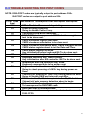
C-3 TROUBLE SHOOTING FOR POST CODES
NOTE: EISA POST codes are typically output to port address 300h.
ISA POST codes are output to port address 80h.
POST Code
(hex)
C2
C5
C6
C7
C8
CA
CB
CD
CE
CF
D1
D2
D3
D4
D5
D0
AMI WinBIOS uncompress code checkpoint Description
NMI is Disable. Power on delay starting.
Power on delay complete.
Going to disable Cache if any.
Calculating ROM BIOS checksum.
ROM BIOS checksum passed. CMOS shutdown register
test to be done next.
CMOS shutdown register test done.
CMOS checksum calculation to be done next.
CMOS checksum calculation done, CMOS Diag byte written
CMOS status register about to init for Date and Time.
CMOS status register init done.
Any initialization before keyboard BAT to be done next.
BAT command to keyboard controller is to be issued.
Keyboard controller BAT result verified.
Any initialization after KB controller. BAT to be done next.
Initialization after KB controller BAT done.
Keyboard command byte to be written next.
Keyboard controller command byte is written.
Going to check pressing of <INS> key during power-on
Done.
Checking for pressing of <INS> key during power-on done.
Going to disable DMA and interrupt controller.
DMA controller #1, #2, interrupt controller #1, #2 disable.
Chipset init/ auto memory detection about to begin.
Chipset initialization/ auto memory detection over.
To uncompress the RUNTIME code.
RUNTIME code is uncompressed.
Transfer control to uncompressed code in shadow ram at
F000: FFF0.
61
61
Runtime code is uncompressed in F000 shadow ram
POST Code
(hex)
01
02
03
05
06
07
08
09
0A
0B
0C
0E
0F
10
11
12
13
15
19
AMI HiFLEX BIOS/WinBIOS runtime code Description.
Processor register test about to start and NMI to be
Disabled.
NMI is Disabled.
Power–on delay starting.
Power on delay complete. To check soft reset /power-on.
Soft reset / power-on determined.
Going to disable Cache if any.
POST code to be uncompressed.
POST code is uncompressed. CPU init and CPU area
init to be done next.
CPU and CPU date area init done.
CMOS checksum calculation to be done next.
CMOS checksum calculation is done, CMOS Diag byte
written. CMOS init to begin (if “init CMOS in every boot”
is set).
CMOS initialization done (if any).
CMOS status register about to init for Date and Time.
CMOS status register init done.
Any initialization before keyboard BAT to be done next.
KB controller I/B free. Going to issue the BAT command
to keyboard controller.
Keyboard controller BAT result verified.
Any initialization after KB controller BAT to be done next.
Initialization after KB controller BAT done.
Keyboard command byte to be written next.
Keyboard controller command byte is written.
Going to issue Pin 23, 24 blacking / unblocking command.
Pin 23, 24 of keyboard controller is blocked / unblocked.
Going to check pressing of <INS> key during power-on.
Checking for pressing of <INS> key during power-on done.
Going to disable DMA and interrupt controllers.
DMA controller #1, #2, interrupt controller #1, #2 disabled.
Video display is disabled and port-B is initialized.
Chipset init about to begin.
Chipset initialization over. 8254 timer test about to start.
8254 timer test over.
About to start memory refresh test.
62
62
1A
20
23
24
25
26
27
28
2A
2B
2C
2D
2E
2F
30
31
32
34
37
38
Memory Refresh line is toggling.
Going to check 15 micro second ON/OFF time.
Memory Refresh period 30 micro second test complete.
Base 64K memory to be initialized.
Base 64K memory initialized. Going to set BIOS stack
and to do any setup before interrupt vector init.
Setup required before interrupt vector initialization
Complete. Interrupt vector initialized about to begin.
Interrupt vector initialization done. Going to read input port
of 8042 for turbo switch (if any) and to clear password if
post diagnostic switch is on.
Input port of 8042 is read.
Going to initialize global data for turbo switch.
Global data initialization for turbo switch is over.
Any initialization before setting video mode to be done next
Initialization before setting video mode is complete.
Going for monochrome mode and color mode setting.
Different BUSes init (system, static, output devices) to
Start if present. (Please see next section for details of
different BUSes).
About to give control for any setup required before optional
video ROM check.
Processing before video ROM control is done.
About to look for optional video ROM and give control.
Optional video ROM control is done. About to give control
to do any processing after video ROM returns control.
Return from processing after the video ROM control.
If EGA/VGA not found then do display memory R/W test.
EGA/VGA not found.
Display memory R/W test about to begin.
Display memory R/W test passed.
About to look for the retrace checking.
Display memory R/W test or retrace checking failed.
About do alternate Display memory R/W test.
Alternate Display memory R/W test passed.
About to look for the alternate display retrace checking.
Video display checking over. Display mode to be set next.
Display mode set.
Going to display the power ON message.
Different BUSes init (input, IPL, general devices) to start
If present. (Please see next section for details about
Different BUSes).
63
39
3A
3B
40
42
43
44
45
46
47
48
49
4B
4C
4D
4E
4F
50
51
52
Display different BUSes initialization error messages.
(Please see Appendix for details of different BUSes).
New cursor position read and saved. Going to display the
Hit <DEL> message.
Hit <DEL> message displayed. Virtual mode memory test
about to start .
Going to prepare the descriptor tables.
Descriptor tables prepared. Going to enter in virtual mode
for memory test.
Entered in the virtual mode. Going to enable interrupts for
diagnostics mode.
Interrupt enabled (if diagnostics switch is on).
Going to initialize data to check memory wrap around at
0: 0.
Data initialized. Going to check for memory wrap around
at 0:0 and finding the total system memory size .
Memory wrap around test done. Memory size calculation
Over. About to go for writing patterns to test memory.
Pattern to be tested written in extended memory.
Going to write patterns in base 640K memory.
Patterns written in base memory.
Going to find out amount of memory below 1M memory.
Amount of memory below 1M found and verified.
Going to find out amount of memory above 1M memory.
Amount of memory above 1M found and verified. Check for
Soft reset and going to clear memory below 1M for soft
Reset. (If power on, go to check point #4Eh).
Memory below 1M cleared. (SOFT RESET) Going to clear
Memory above 1M.
Memory above 1M cleared. (SOFT RESET)
Going to save the memory size. (Go to check point #52h).
Memory test started. (NOT SOFT RESET) About to display
The first 64k memory size.
Memory size display started. This will be update during
Memory test. Going for sequential and random memory
Test.
Memory testing/initialization below 1M complete.
Going to adjust displayed memory size for relocation/
Shadow.
Memory size display adjusted due to relocation/shadow.
Memory test above 1M to follow.
Memory testing/initialization above 1M complete.
Going to save memory size information.
64
53
54
57
58
59
60
62
65
66
67
7F
80
81
82
83
84
85
86
87
88
89
Memory size information is saved. CPU register are saved
Going to enter in real mode.
Shutdown successful, CPU in real mode.
Going to disable gate A20 line and disable parity/NMI.
A20 address line, parity / NMI disable successful.
Going to adjust memory size depending on relocation /
Shadow.
Memory size adjusted for relocation / shadow.
Going to clear Hit <DEL> message.
Hit <DEL> message cleared. <WAIT …> message displayed
about to start DMA and interrupt controller test.
DMA page register test passed. To do DMA#1 base Register
Test.
DMA#1 base register test passed. To do DMA#2 base
Register test.
DMA#2 base register test passed. To program DMA unit
1 and 2.
DMA unit 1 and 2 programming over. To initialize 8259
Interrupt controller.
8259 initialization over.
Extended NMI sources enabling is in progress.
Keyboard test started. clearing output buffer, checking
For stuck key, About to issue keyboard reset command.
Keyboard reset error / stuck key found.
About to issue keyboard controller interface test command.
Keyboard controller interface test over.
About write command byte and init circular buffer.
Command byte written, Global data init done.
About to check for lock-key.
Lock-key checking over. About to check for memory size
Mismatch with CMOS.
Memory size check done. About to display soft error and
Check for password or bypass setup.
Password checked. About to do programming before
Setup.
Programming before setup complete.
Going to uncompress SETUP code and execute CMOS setup
Returned from CMOS setup program and screen is cleared.
About to do programming after setup.
Programming after setup complete.
Going to display power on screen message.
65
65
8B
8C
8D
8E
8F
91
94
95
96
97
98
99
9A
9B
9C
9D
9E
9F
A0
A1
A2
A3
A4
First screen message display. <WAIT…> message
Displayed. About to do Video BIOS shadow.
Video BIOS shadow successful. Setup options
Programming after CMOS setup about to start.
Setup option are programmed, mouse check and init to be
Done next.
Mouse check and initialization complete. Going for hard
Disk controller reset.
Hard disk controller reset done.
Floppy setup to be done next.
Floppy setup complete. Hard disk setup to be done next.
Hard disk setup complete. To set base and extended
Memory size.
Memory size adjusted due to mouse support. Init. of
Different BUSes optional ROMs from C800to start.
(Please see next section for details of different BUSes).
Going to do any init before C800 optional ROM control.
Any init before C800 optional ROM control is over.
Optional ROM check and control will be done next.
Optional ROM control is done. About to give control to do
Any required processing after optional ROM returns control
Any initialization required after optional ROM test over.
Going to setup timer data area and printer base address.
Return after setting timer and printer base address.
Going to set the RS-232 base address.
Returned after RS-232 base address.
Going to do any initialization before Coprocessor test.
Required initialization before Coprocessor is over.
Going to initialize the Coprocessor next.
Coprocessor initialized. Going to do any initialization after
Coprocessor test.
Initialization after Coprocessor test is complete.
Going to check extd keyboard , keyboard ID and num-lock .
Extd keyboard check is done, ID flag set, num-lock on/off
Keyboard ID command to be issued.
Keyboard ID command issues. Keyboard ID flag to be reset
Keyboard ID flag reset. Cache memory test to follow.
Cache memory test over. Going to display any soft error.
Soft error display complete.
Going to set keyboard typematic rate.
Keyboard typematic rate set. To program memory wait
States.
66
A5
A7
A8
A9
AA
B0
B1
00
Memory wait states programming over.
Going to clear the screen and enable parity / NMI.
NMI and parity enabled.
Going to do any initialization required before giving control
To optional ROM at E000.
Initialization before E000 ROM control over. E000 ROM to
Get control next.
Returned from E000 ROM control.
Going to do any initialization required after E000 optional
ROM control.
Initialization after E000 optional ROM control is over.
Going to display the system configuration.
System configuration is displayed.
Going to copy any code to specific area.
Copying of code to specific area done. Going to give control
To INT-19 boot loader.
67
67
The system BIOS gives control to different BUSes at following checkpoints to
do various tasks on the different BUSes.
POST CODE
(HEX)
2A
38
39
95
AMI HiFLEX BIOS /WinBIOS Checkpoints of the BUSes
Different BUSes init (system, static, output devices)
To start if present.
Different BUSes init (input, IPL, general devices)
To start if present.
Display different BUSes initialization error messages.
Init of different BUSes optional ROMs from C800 to start.
While control is inside the different BUS routines, additional checkpoints are output
to port 80h as WORD to identify the routines under execution. These are WORD
checkpoints, the LOW BYTE of checkpoint is the system BIOS checkpoint from
where the control is passed to the different BUS routines and the HIGH BYTE of
checkpoint is the indication of which routine is being executed in the different BUSes.
The details of HIGH BYTE of these checkpoints are as follows:
HIGH BYTE XY
The upper nibble ‘X’ indicates the function # is being executed. ‘X’ can be from 0 to 7.
0 = func#0, disable all device on the BUS concerned.
1 = func#1, static devices init on the BUS concerned.
2 = func#2, output device init on the BUS concerned.
3 = func#3, input device init on the BUS concerned.
4 = func#4, IPL device init on the BUS concerned.
5 = func#5, general device init on the BUS concerned.
6 = func#6, error reporting for the BUS concerned.
7 = func#7, add-on ROM init for all BUSes.
The lower nibble ‘Y’ indicates the BUS on which the different routines are being
executed. ‘Y’ can be from 0 to 5.
0 = Generic DIM (Device Initialization Manager)
1 = On-board System devices.
2 = ISA devices.
3 = EISA devices.
4 = ISA PnP devices.
5 = PCI devices.
68
68