1
FLT
V4
User Manual
Project: KATRIN
Version 3.1
Denis Tcherniakhovski
17 April 2013
Contents
1.
2.
3.
4.
5.
6.
Introduction ........................................................................................................................ 3
Trigger Concept.................................................................................................................. 3
Subrack Architecture.......................................................................................................... 4
Backplane ........................................................................................................................... 5
FLT Architecture................................................................................................................ 6
KATRIN: Modes of Operations......................................................................................... 7
Run Mode I - standard mode .............................................................................................. 7
Run Mode II
- histogram mode........................................................................................ 7
Test Mode............................................................................................................................... 7
7. A/D Conversion.................................................................................................................. 8
8. Control of Analog Board.................................................................................................. 10
Gain & Offset Settings. Sequence of Settings (IPE-AB). .................................................... 10
Test Pulse Circuit ................................................................................................................. 11
9. Filter Unit ......................................................................................................................... 12
10.
Pixel Trigger Handling................................................................................................. 14
Timer Unit ............................................................................................................................ 15
Pixel Trigger Transmission to SLT...................................................................................... 15
11.
Trigger Data Storage (internal DP-RAM).................................................................... 16
12.
ADC Data Storage (1M x 18bit QDRII) ...................................................................... 19
ADC Data Format ................................................................................................................ 19
ADC Page Management....................................................................................................... 19
13.
Histogram Unit............................................................................................................. 20
14.
Hit Rate Measurement.................................................................................................. 22
15.
Interrupt Logic.............................................................................................................. 26
16.
KATRIN: FLT Register Overview .............................................................................. 27
17.
In-Crate Communication. PE-Bus................................................................................ 32
18.
FLT Address Map ........................................................................................................ 33
19.
Clock Distribution. Synchronization Schema. ............................................................. 34
20.
Abbreviations ............................................................................................................... 35
21.
References .................................................................................................................... 35
22.
Appendix A .................................................................................................................. 36
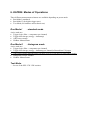
1. Introduction
.
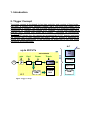
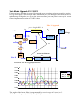
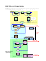
2. Trigger Concept
The trigger concept is developed for fast data reduction and consists of three levels first (FLT) & second level hardware triggers (SLT) and third level trigger (TLT)
implemented in software. The total front-end electronics of a telescope housed in a
commercial 19’’ subrack that consists of 21 modules - 20 first level trigger (FLT)
modules and 1 second level trigger (SLT) module - connected via monolithically
backplane.
The 440 PMT signals from the camera are processed by 20 FLT boards (one board
per column) with 22 input channels per board. The FLT module is partitioned by
analog and digital submodules. In the following the digital part of first level trigger
electronics will be described.
SLT
ETH
up to 20 FLTs
gain
Cntrl
24 channels
Param.
Thresh.
emb.
PC
TimeMgr
ADC
Filter
Trigger
Timer
RAM
FLT
Figure. Trigger Concept
Control
Unit
SysCntrl
RAM
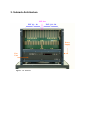
3. Subrack Architecture
SLT slot
FLT # 1.. 10
FLT # 11.. 20
Power
Supply
Fan
Unit
Figure 1. 19`` Subrack
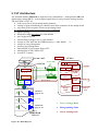
4. Backplane
±5V,2.5V analog
3.3V dig
Vtt
Vtt
GTLP control bus
FLT
# 1
FLT
# 10
SLT
FLT
# 20
FLT
# 11
M-LVDS bus (16 bits + 4 cntl) @40MHz Æ 80MB/s
Clk20MHz
1 x10
FanOut
M-LVDS – Multipoint LVDS
Figure 2 Backplane Block Diagram
PTrigger bus
LVDS 240 Mb/s
1 x 10
FanOut
GTLP - Gunning Transceiver Logic Plus
5. FLT Architecture
The frontend module (FEboard) is separated in two submodules – Analog Board (AB) and
digital trigger board (FLT) – to keep digital signal lines far away from the analog circuitry.
The main tasks of FLT are
• A/D conversion of 24 incoming analog channels
• settings of gain (individually per channel) and offset (common) on the analog board
• activation of the test pulse circuits on the analog board
• on-board background measurement (noise evaluation)
• digital filtering
• threshold setting and control for each channel
• pixel trigger detection
• measurement of trigger rate for each channel
• storage of ADC data into the QDRII memory (= ADC RAM)
or
• storage of energy histograms
• memory page management
• transmission of pixel trigger data to SLT
• transmission of ADC data to SLT
• overall FLT control
wrPointer
3 x 8ch. ADC
ADC
CFPGA
24 ser. links
EF FF fill_pointer
3 x FPGA8
Event table
300ns
Energy Ch 1
Controller8
Filter/Trigger
Energy Ch 24
Page
counters
20 + 2 bit pu
Data Bus 32bit
Page
Histogram
counters
Unit
24 x
ADC
Hit Rate
RAM
300ns
Filter/Trigger
Page table
24 x
Histograms
Energy
RAM
CNTRL
Unit
Ser.
Transmit
Channel 1
pages 0…63
...
Channel 24
pages 0…63
3x
QDRII RAM
1M x 18
Figure. FLT Block Diagram
OnePPS
channels timestamp
20 + 2 bit pu
...
...
Timer
•
Trace + Energy Mode
•
Histogramming Mode
•
always running tasks
PE-Bus
Link to
SLT
6. KATRIN: Modes of Operations
Three different measurement schemas are available depending on preset mode:
• Run Mode I (standard)
• Run Mode II (for higher trigger rates)
• Test Mode (for hardware and software test)
Run Mode I
- standard mode
Active tasks are:
• Trigger logic (filter + comparator per channel)
• Trigger data storage (energy + timestamp)
• ADC traces storage
• Hit Rate Measurement
Run Mode II
- histogram mode
Active tasks are:
• Trigger logic (filter + comparator per channel)
• Trigger data storage (energy + timestamp per channel) allocated into 128 pages
• ADC traces storage allocated into 128 pages a 50 us (or 64 pages a 100us and so forth)
• Histogram Unit per channel
• Hit Rate Measurement
Test Mode
… for test of the HW / FW / SW routines.
7. A/D Conversion
ADC SPI port [ADC]
PCI address space = 0x000400... 0x0007FC
256 Registers
Table 15.
Memory Map
Register
Addr.
(Hex)
Param.
Name
Bit 7
(MSB)
Bit 6
Bit 5
Bit 4
Bit 3
Bit 2
Bit 1
Bit 0 (LSB)
chip_port
_config
0
LSB
first
1 = on
0 = off
(def.t)
Soft
reset 1 =
on 0 = off
(default)
1
1
Soft
reset 1 =
on 0 = off
(default)
LSB first
1 = on 0
= off
(default)
0
chip_id
8-bit Chip
ID Bits 7:0
(AD9222 =
0x07),
(default)
Default Notes/ Comments
Chip
Configuration
Registers
00
The nibbles
should be
mirrored so that
LSB- or MSBfirst mode
registers
correctly
regardless of
shift mode.
Default is unique
chip ID, different
for each device.
This is a readonly register.
01
02
chip_grade
X
Child ID 6:4
(identify
device
variants of
Chip ID) 011 =
50 MSPS 001
= 40 MSPS
X
X
X
X
Child ID used to differentiate graded devices.
Device Index
and Transfer
Registers
04
device_in
dex_2
X
X
X
X
Data Channel
H 1 = on
(default)
0 = off
Data
Channel
G 1 = on
(default)
0 = off
Data
Channel
F 1 = on
(default)
0 = off
Data
Channel E
1 = on
(default) 0 =
off
Bits are set to
determine which
on-chip device
receives the next
write command.
05
device_in
dex_1
X
X
Clock
Channel
DCO 1 =
on 0 = off
(default)
Clock Channel
FCO 1 = on 0
= off (default)
Data
Channel
D 1 = on
(default)
0 = off
Data
Channel
C 1 = on
(default)
0 = off
Data
Channel
B 1 = on
(default)
0 = off
Data
Channel A
1 = on
(default) 0 =
off
Bits are set to
determine which
on-chip device
receives the next
write command.
FF
device_u
pdate
X
X
X
X
X
X
X
SW transfer
1 = on
0 = off
(default)
X
X
Synchronously transfers data from the master shift register to the slave.
ADC Functions
08
modes
X
X
X
Internal
powerdown mode
000 = chip
run (default)
001 = full
powerdown 010 =
standby
011 = reset
Determines
various generic
modes of chip
operation.
09
Turns the
internal duty
cycle stabilizer
on and off.
0D
clock
X
X
X
X
X
test_io
User test
mode
00 = off
(default)
Res
et
PN
long
gen
1=
on 0
= off
(def
ault)
Reset PN
short gen 1 =
on 0 = off
(default)
Output test mode—see Table 9 in the Digital
Outputs and Timing section 0000 = off (default)
0001 = midscale short 0010 = +FS short 0011 =
−FS short 0100 = checker board output 0101 =
PN 23 sequence 0110 = PN 9 0111 = one/zero
word toggle 1000 = user input 1001 = one/zero bit
toggle 1010 = 1× sync 1011 = one bit high 1100 =
mixed bit frequency (format determined by
output_mode)
01 = on,
single
alternate
10 = on,
single once
11 = on,
alternate
once
When set, the test data is placed on the output pins in place of normal data.
Deserializer
X
X
Duty cycle
stabilizer 1
= on
(default) 0 =
off
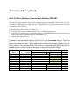
8. Control of Analog Board
Gain & Offset Settings. Sequence of Settings (IPE-AB).
Several gains and common offset on the analog board are controlled by three octal (3*8=24)
12bit DACs MAX5306 (for gains) and one 12bit MAX5530 (for offset) connected as a chain
via SPI bus to the CFPGA.
Gain and Offset values may be set / read as
• a block of 25 words (a common offset word + 24 individual gains) or
• sequence of single access to OffsetAddr address (0x00080000) followed by a block of 24
gains addressed to GainStart address (0x00080001) or
• sequence of single accesses
Loading of data starts after setting of bit 8 (LG) in the Command register. The load
routine takes about 150us (due to slow serial data transmission). Accessory, new
gains are stable only after ~30ms settling time (caused by blocking capacitor on the
DAC outputs). The summary delay (30.150 ms) is indicated by the busy flag (bit 8 in
Status register). Note: Avoid any accesses to the gains while first 150us!
PCI Addr
base
0x00080000
0x00080004
0x00080004
0x00080004
0x00080004
Chan
#
0
23
Table GainRAM Format
Addr
RAM
0x00
0x01
…
…
0x18
0x19
0x1A
0x1B
0x1C
Data
31
-
- - - - - - - - - - - - - - - - - - - - - - - - - - - - - - - - - - - - -
15
-
11 . . . . . 0
Offset
Gain Ch1
Gain Ch2
- - - - - Gain Ch24
0x8000 update offset
0xFFFF update gains
0xFFFF update gains
0xFFFF update gains
default
0x0800
0x0800
0x0800
- - - 0x0800
0x8000
0xFFFF
0xFFFF
0xFFFF
Test Pulse Circuit
The test pulses are used to test the analog channels and trigger logic. The SLT
module provides the pulse shape and timings, the FLT switches the several channels
on / off depending on the test pattern stored in the internal memory.
The internal FIFO TP_MEM consists of 128 words of 25-bits (22+2 outputs + repeat
flag). Each word represents the state of the 22 test pulses outputs. The 50ns long
strobe on the TPulse line forces the next memory word (AND-masked with
TestPulseEnable) to be put on the FPGAs output and increments the address
afterwards. The bit 24 (= repeat flag) marks the end of pattern and cause the restart
of read pointer. This may be used to build the repeat-loops.
A write of 0x02------ (data bit25 = 1) to any gain address causes a reset of the read
pointer.
TP_switch = TP_MEM_OUT AND TestPulseEnable;
TP_EN = 0 when TestPulseEnable = 0;
The amplitude and shape of the pulse are given by the SLT module. The output of
test pattern is delayed with respect to begin of the TPulse-strobe by 100ns.
The TP_MEM can be used as well as direct test pattern for the pixel trigger, if
registers PixelTriggerMode, PixelSettings1, PixelSettings2 are set accordingly (see
Pixel Trigger Unit). In this case each 24bit pixel trigger word is replaced by 24 output
bits of TP_MEM.
TestPatMem
- Test Pattern Memory 128x32
PCI address = 0x001100
Addr. 31 26 25
24 23
0x00
0
rst
rep
Test pattern (first)
0
rst
rep
…
0
rst
rep
…
0x7F
0
rst
rep
Test pattern 128
Table TP_MEM Format
0
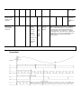
9. Filter Unit
Two cascaded FIR shaping filters are used in the actual KATRIN
design to provide the accurate amplitude (Filter I) and time
stamp (Filter II) of a pulse. A pixel trigger occurs when the
extracted amplitude (represents the energy of particle) exceeds
the threshold (adjustable). Both filter parameters – shaping time
L and gap length N - are adjustable as shown below:
L
L
N
Frequency Response, 1st stage
Parameter
Label Range Interpretation
ShapingTime L
2..8
L2 : 2Æ4, 3Æ8, 4Æ16, 5Æ32, 6Æ64, 7Æ128, 8Æ256
GapLength
N
0..7
N : 0..7 Note: N=0 if LÆ256
All parameters are in units of the time atom (50ns).
ADCdata
Z –(L)
Z -N
+
+
Z –(L)
-
-
1
1 − Z −1
+
1
1 − Z −1
+
X
+
X’ = (X *
coeff_x_128)
>>7;
coeff_x_128
Filter I
Z –L/2
Energy
Z –L/2
x2
-
+
+
+
+
Filter II
1
1 − Z −1
Filter & Pixel Trigger Implementation
&
zero cross detector
<0
1 – Z -1
Trigger
+
> Thresh
An internal FIFO is used for delay element Z-x. The depth of FIFO is limited to 512, so
maximal delay (2 * shaping time + gap length) is 512. This means also that settings
of ShapingTime = 8 (256) and a gap non-zero would excess the maximal FIFO
length. To avoid the overflow - when ShapingTime is set to 256 - the GapLength
parameter will reset automatically and an warning flag at bit2 of PStatus is set.
PCI address = 0x00000038
Bits
Function
Description
Bit 0
StoreData
store data into external RAM (QDRII)
Bit 1
RunADC
start ADC sampling
Bit 2
FilterRun
run the filter unit
Bit 3
TriggerRun
run the trigger unit
[07:04] GapLength
max. 7!
[13:08] ShapingTime min. 2! shaping time
[27:24] PoleZeroCorr 0..15 correction factor (0 – no correction – default)
[31:16]
reserved
Table RunParam Register
PCI address = 0x00002080
31
20
19
0
Threshold (channel i)
Table Threshold Format
The second trigger condition
occurs when sloping curve of
Filter_II crosses zero.
The gradient at zero point
determines the most precise time
point as given be clock of
20Mhz. This allows a time stamp
resolution of tcyc / 2 = 25 ns.
The time precision bit marks the
appropriate half:
‘0’ - left half
‘1’ - right half
1200
1000
800
600
400
200
0
115
25k
130 140 150 160 170 180 190 200 210 220 230 240 251
20k
threshold
15k
energy
The measured energy is the
height of trapeze (triangle if
GapLength=0) delivered by first
stage of the filter.
The first condition is
met
because of energy > threshold.
ADC trace
ShapingTime = 4 (2 = 16),
GapLength = 5 and
Threshold
= 19200.
1400
Filter_I out
4
1600
10k
5k
0
-5k
120k
Filter_II out
An example right shows behavior
of the filter parameterized with
tleft
50k
tcyc
0
-50k
-120k
zero crossing
tright
Pole-Zero Correction
without pole-zero correction
pole-zero correction (coeff = 0.836)
Settings Format bits[27:24] of RunControlRegister
settings
15
14
13
12
11
10
9
8
7
6
5
4
3
2
1
0
attenuation
0,695
0,719
0,734
0,758
0,773
0,797
0,813
0,836
0,859
0,875
0,898
0,914
0,938
0,953
0,977
1,000
coeff_x_128
89
92
94
97
99
102
104
107
110
112
115
117
120
122
125
128
none (default)
10. Pixel Trigger Handling
A Pixel Trigger occurs in FPGA8 when filter output exceeds the threshold. A trigger
bit as well as energy value and two time precision bits packed to a word are sent
serial (each channel individually) to CFPGA to store there the trigger data, measure
the hit rate and to send these further to the SLT via 240Mbit/s serial LVDS link.
The transmission of a word takes 300ns, so the equal dead time after a trigger is to
respect for the very short filter lengths (<2). When the CFPGA detects the first bit of a
trigger telegram it takes the actual timer state and stores this together with received
data into EventFIFO.
Timer Unit
The timer in CFPGA consists of two counters:
• 32 bit second counter and
SLT: SecStrb
• 25 bit subsecond counter
The second counter can be set by SW FLT: SecStrb
and increments with every SecStrobe
SecCount
pulse. The subsecond counter runs with
internal 20MHz clock and restarts after
SubSecCount
every SecStrobe pulse. Therefore first
second is always to waiting for
synchronization after each start of run mode I.
second (i)
N-1
N
second (i + 1)
0
1
Pixel Trigger Transmission to SLT
The CFPGA sends a pixel trigger word filled out with start and parity bits to the
central card (SLT) every 100 ns. The start of transmission is synchronized to the
internal 10MHz.
23 22
1 00
S
Pixel Trigger[21:00]
P
Table Pixel Trigger Link. Data Fomat.
S
Start Bit ‘1’
P
Parity Bit (odd)
Several pixel triggers can be tied to a fixed value or replaced by different test pattern
before sending to SLT. This may be useful to mark the damaged pixels and for tests.
Both PixelSettings1&2 registers define the state of the outgoing pixel triggers:
PCI address
0x000030
0x000034
31
22
0
0
21
0
LSBits[21:0]
MSBits[21:0]
Table PixelSettings1/2 Registers
The state of a pixel trigger is defined as:
MSBit LSBit Pixel Trigger Output
0 0
normal state
0 1
test pattern taken from the TestPatternMem
1 0
always 0
1 1
always 1
11. Trigger Data Storage (internal DP-RAM)
For each trigger event following data should be stored for readout:
• energy interpretation of event
• precise time stamp of occurrence
• to 100 us deep corresponding ADC trace (in Run_I mode only, else histogram)
The paging schema is used to handle the bursts of triggers. The page lengths are
512/64 per board and 64 per channel. All incoming pixel trigger are OR-ed together
to an overall trigger event whose occurrence causes an increment of the write pointer
and storage the appropriate data into the EventFIFO, consists of EventTable and
PageTable (see below).
EventFIFO is organized as FIFO (depth of 512/64 ) , so only one (latest) item can be
read by SW. Event Status register shows the current number of triggers (= write
pointer) and read accesses (= read pointer). The overflow behavior of the FIFO is
selected by setting of bit 24 of Control Register:
‘1’ – stop when full,
‘0’–enable overflow
The depth of EventFIFO is selectable by setting of bit ControlReg[25]:
‘1’ – 64,
‘0’– 512
EventFIFO Status Register
29 28 25
AE EF
read pointer
16
13 12 9
FF AF
0
write pointer
While ‘fifo not empty’ is observed, the program reads the last entry consisting of time
stamp and channel list (multiple pixels can trigger simultaneously), decides on the
channel number and gets then (under specification of channel number) the
corresponding page number. When channel and page indexes are known,
appropriate energy and ADC trace data can be read (ADC data in Run_I mode only).
Event Table (512x96)
11 blocks
addr
Channel Map
EventID
Time Stamp
(9bit)
(24bit)
(12bit)
Seconds (32bit)
Subseconds (25bit) ,
95 ……………… 72 71 …. 49 48…….….…….27 26 …………..…. 2 1..0
8 .. 0
0
1
---x----x-----xx----xx-2
511
Page Table (512 x 24channels x 6bit )
16 blocks
Event
Page Number of Channels 1... 24
ID
1 2 3 4 5 6 7 8 9 10 11 12 13 14 15 16 17 18 19 20 21 22 23 24
0
1
2 - - - N - - - - N - - - - - N N - - - - N N - -
N
511
Energy Table (per channel)
Page N
0
1
24 blocks
Energy (20bit)
63
ADC traces (per channel)
Page N
0
1
63
extern. QDR RAM
ADC traces
block of 2048 ADC samples a 16 bit
block of 2048 ADC samples a 16 bit
block of 2048 ADC samples a 16 bit
Event Handling Procedure
Observe the event status
read EventFIFOstatus
empty
not empty
Handle event i
Event loop
Event i
Read EventTable
Get the channel list a time stamp
Which channel(s) has(have) triggered?
Select channel number
read EventTable
TimeStamp i
Channel List
ChannelN
Channels loop
Channel j
Event i
Get the page number
read PageTable
Page k,
Channel j
Read corresponding energy
read Energy
Page k,
Channel j
Energy i
TimeStamp i
read ADCtrace
ADC trace i
Read corresponding ADC data
If multichannel trigger select next channel
12. ADC Data Storage (1M x 18bit QDRII)
ADC Data Format
Three 1Mx18 synchronous QDRII RAMs are used to store the ADC data of 24
channels. The address space of each SRAM is partitioned into 64 pages a 2K words.
Normally (no trigger occurred) the ADC data are written into the actual page
organized as a ring buffer (depth 2048). The 2K data frame as shown below consists
of the ~100us history and may be read out as block or via single.
Each data word consist of 12 bit ADC data and four auxiliary flags:
15
14
13
12 11
PT Inh AF
ADC Value 0 .. 4095
Pixel Trigger flag
global Inhibit flag
Append this Page flag
readout page
NxtPage
read address
bit 15 14
0 1
0 1
0 0
0 0
0 0
1 0
0 0
11
0
ADC
samples
2048 words - 100us
PT
Inh
AP
0
AppendThisPage
Inhibit flag
actual page
write address
Pixel Trigger
ADC Page Management
Each channel has a simplified page management implemented as a free running
trigger counter. The number of the actual page (0...63) equates to the trigger count
(0...63) which increments delayed after post-trigger time (PostTrigTime). When a
next trigger (i+1) occurs during the
post-trigger time of previous
AppendThisPage flag
trigger (i), the page number
increases immediately (i+1) and
Page i + 1
Page i
flag AppendThisPage (bit13) is
set to mark the pile-up.
Ti
Ti+1
TPostTrigTime
13.
Histogram Unit
For higher trigger rates (above ???kHz) the standard mode (Run_I) is not capable
handling several events. The histogram mode (Run_II) can be used in order to
determine the energy distribution of each channel.
Histogramming Schema
The energy range and resolution are adjustable using E_Min and E_Bin parameters
to get a best fit to expected energy spectrum. To limit the readout time two margins
FirstEntry and LastEntry marking an area that contains data are calculated by
hardware. Every bin of the histogram contains a 32 bit counter.
B0
first
Bi
last
BN-1
in range
E_Min
E_Max
If e(i) is the measured energy of a trigger (i), then the appropriate bin is calculated as
Bi = (e – E_Min) >> E_Bin
All triggers that don’t match the defined range will be absorbed into the bins B0 and
BN-1 respectively. If no triggers are observed during the measurement period
HistMeasTime, ‘page not empty’ flags in pStatus registers remain zero.
The histogram building works without dead-times during readout. For this reason two
memory fields (two pages) are used per channel – one working area to build the
actual histogram and one containing last measurements for readout. Both pages are
toggled after programmable time HistMeasTime.
Bits 29…28 – bit28 histogram mode HM and bit 29 clear mode CM - determinate
behaviour of the histogram unit. At the end of measurement period the readout page
can be cleared to cleanup the old data and begin the histogram ab initio. The cleanup
can start either automatically by hardware (clear mode CM = ‘0’) or by user (CM=’1’).
If the readout page was not cleared by user (in clear mode ‘1’) in sufficient time the
histogram unit stops when HM = ‘1’. Set the CM=’1’ and HM=’0’ causes further
accumulating of histograms. The ‘age’ of a histogram is shown in registers
HistRecTime and HistNofMeas.
Programmable settings:
E_Min
HistgrSettings [19:00]
E_Bin
HistgrSettings [23:20]
HistMeasTime
HistMeasTime[31:00]
HM
HistgrSettings [28]
histogram begin
0...15 Æ 0, 1, 2, 4, 8, 16... 32K
0...2^32-1 sec
histogram mode: ‘0’ continuous,
‘1’ stop if not cleared before
clear mode: ‘0’ automatically,
‘1’ clear by user
CM
HistgrSettings [29]
Control bits:
CLR
Command[17]
clear histogramming page
Status:
HistRecTime
HistNofMeas
FirstEntry
LastEntry
page not empty
HistRecTime
HistNofMeas
HistLastFirst[15:00]
HistLastFirst[15:00]
pStatusABC[19:12]
second counter 0…HistMeasTime-1
number of measurement cycles
first bin
last bin
a flag per channel
Fixed parameters:
N_of_bins
= 2048
MaxHistCount
= 2^32-1 (32bit)
Timing:
HistMeasTime in seconds
stop
Page B
Page A
Readout Page B
Page B
Page A
Readout Page B
Page B
clear page B
mode ‚0’
continuous
stop
mode ‚1’
stop if not cleared
14. Hit Rate Measurement
The trigger rate is measured periodically for all enabled channels. The measurement
time is programmable in range of Tcount = 1, 2, 4, 8, 16 or 32 sec.
The overflow of some counters will cause an interrupt flag. The hit rate measurement
is disabled after reset and can be started for each channel separately by setting
HitRateMeasEnable register. While Veto is active all hit rate counters keep
unaltered.
PCI start address = 0x00080100
31
24
16
15
HRover
HitRate (Hz)
0
Table Hit Rate Memory Data Format
PCI address 0x00000048
31
24
16 15
TtrigLength
3
0
Tcount
Table HitRateMeasParameters
Tcount = 0 .. 15 (0 Æ 1 sec, 2 Æ 2sec, 3 Æ 4sec, 4 Æ 8sec, 5 Æ16sec, 6 Æ 32sec)
PCI address 0x00000024
31
23
Enable Bits : ‘1’ enabled, ‘0’ disabled
Table HitRateMeasEnable
0
15. Veto Mode
Channel Trigger Building
The veto triggering concept makes use of short pulse shape of signals.
In Veto Mode the first filter stage is bypassed to the second stage. The filter becomes a
triangle function as shown below.
The ‘shaping time’
and
threshold
should
be
set
adequately.
Note that the energy
value in this mode
corresponds to the
absolute
pulse
amplitude
(with
offset).
2110
2100
2080
2060
2040
2030
120
50
0
-50
-120
Pair Trigger
The pair trigger based on coincidence of two channels corresponding to two ends of a fiber.
The coincidence time is programmable in range of -200ns … 200ns. However the pair
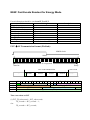
assignment is fix. All 24 pixel per FLT board 1..24 build 12 pairs:
{(1,3), (5,7), (9,11), (13,15), (17,19), (21,23), (2,4), (6,8), (10,12), (14,16) (18,20), (22,24)}
Trigger
Ch i
Trigger
Ch i+1
Pair
Trigger
Chi
Pair
Trigger
Chi+1
T_over
Sum and Coincidence Triggering
The veto triggering schema based on coincidence of at least N channels (fiber ends) with an
analog sum of all six inputs. The sum building occurs outside the crate (analog). Coincidence
window and N are programmed in range of 0..250ns in 50ns steps and 0 to 7 respectively.
Note that the involved thresholds should be adopted appropriate and the numbers of involved
channels is fixed (see below).
FLT group
Group1:
Group2:
Group3:
veto channels
00, 02, 04, 06, 08, 10
16, 18, 20, 22, 01, 03
09, 11, 13, 15, 17, 19
sum channel
14
07
23
sum
channel
Δ−prolong
Filter
chan.
Unit
trigg.
(stage 2)
channels
0..5
unused channel
channel 12 = 0
channel 05 = 0
channel 21 = 0
thresholds
0..5
6
Δ−prolong
&
Σ of bits
coincidence
time window
0 ..250 ns
Figure 3 Sum & Coincidence Trigger. Block Diagram.
Further processing of veto triggers is identical to the standard mode.
RunControl
- Global Settings / Run Parameters
PCI address = 0x000038
Bits
Function
Description
Bit 0
StoreData
store data into external RAM (QDRII)
Bit 1
RunADC
start ADC sampling
Bit 2
FilterRun
run the boxcar filter & trigger units
Bit 3
reserved
[07:04] GAP length length of filter gap
[13:08] FilterLength min. 2 ! shaping time
[15:14] 00
reserved
[19:16] overlap
veto overlap time 0..5 Æ 0..250 ns
[23:20] n-fold
n-fold 0 ..7
[31:24]
reserved
≥
N-fold
Veto
Veto Mode Upgrade 23.11.2012
Existing trigger algorithm is updated, because the zero-cross time point was sensitive to noise
for very short pulses. Now delayed ADC data stream (Ad) runs through a short boxcar filter to
make flat top of the pulse (see Af), so the zero-cross time point can jitter for one cycle. Boxcar
filter is implemented as sum of N ADC values.
Filter I - bypassed
progr. length BL=1..4
Ad
ADCdata
Af
boxcar sum
FF
Energy
Z –L/2
> Thresh
x2
+
+
+
Z –L/2
-
new
&
+
+
Filter II
1
1 − Z −1
Trigger
zero cross detector
Z –BL/2
1 – Z -1
<0
Veto Mode: Filter & Trigger Implementation
2110
2100
ADC
2090
ADC_d
2080
ADC_f
2070
2060
2050
2040
2030
794 796
798
800
802
804
806
808
810
812
814 816
The length of the boxcar filter is programmable by user in range of 0 (none) to 3.
Æ RunControl register (0x000038) bits [15:14]
Interrupt Logic
Two-level interrupt mechanism is implemented at the FLT hardware layer. Level 0
interrupt (transmitted via INT line) signals some error cases in FLTs.
Four possible error flags – bits [3:0] - are allocated for it.
Level 1 interrupt (SpareOut P2.D2 line) is used to inform SLT about the transaction
status.
Interrupt signals on the backplane are active (low) when
INT
= IntrptSources[3:0] & not IntrptMask[3:0]
SpareOut
= IntrptSources[7:4] & not IntrptMask[7:4]
PCI address = 0x000014
31
29 28
24
000
Slot ID
--RO
23
16
0x00
---
15
8 7
Intrpt Mask
RW
0
Intrpt Sources
RO
Table Interrupt Register. Bit Settings.
Interrupt Sources
Bit 0
ConfigError
Bit 1
SyncError
Bit 2
HitRateOver
Bit 3
ParamError
Bit 4
Action1Done
Bit 5
Action2Done
Bit 6
Actios3Done
Bit 7
Action4Done
Error0: FPGA configuration failed
Error1: Second strobe in an unexpected time window
Error2: hit rate counter(s) overflow
Error3: settings conflict
16.
KATRIN: FLT Register Overview
Status
– FLT Module Status Register
PCI address = 0x000000
31
IRQ
h
Clr
h
Pg
F
F
A
F
A
E
E
F
23
16 15 9 8 7 6
interrupt
Bsy AB
sources
HW
54
AB
FW
3
U
P
2
P
2
1
P
1
PF
P1
P2
UP
ABFW
ABHW
SNE
Bsy
power fail
PLL1 unlocked
PLL2 unlocked
unlock phase 10MHz
Firmware: type of analog board
Hardware: type of analog board
BoardID error flag
action busy flag
EF
AE
AF
FF
eventFIFOstatus: empty flag
eventFIFOstatus: almost empty flag (mode512 : <16, mode64 : <4)
eventFIFOstatus: almost full flag (mode512 : >447, mode64 : >55)
eventFIFOstatus: full flag
hPg
hClr
histogram page toggle bit
histogram cleared flag
IRQ
interrupt request
00
01
10
11
0
P
F
FZK HEAT
FZK KATRIN
FZK USCT
ITALY HEAT
Control
- FLT Module Settings
PCI address = 0x000004
31
25 24 23
20 19 16 15
5
4
3 2
1
0
fBeh
mode
TPE 0 LED stby
LED set 1 to switch LED off
stby FLT standby mode
TPE enables the Test Pulse activities
mode mode of operation: ‘00’ – standby, ‘01’ – Run_I, ‘10’ – Run_II, ‘11’ – test
fBeh FIFO behaviour : ‘0’ – enable overflow, ‘1’ – stop when full
Command
- FLT Command Register
PCI address = 0x000004
31
swTr
rstTP
swR
LG
rPoint
rstPg
swTr
17
16
rstPg rPoint
reset TestPulse pointers
set interrupt request (for test)
load gains now
reset pointers
reset pages
SW trigger
8 7
LG
5
4
3
rstTp
2
1
0
swR
Version Number
– FLT Version Management
PCI address = 0x00000C | 0x000010
PCI Addr
31
Version Number
15
8 7
0
0x0000000C Project N
Doc Revision
Version
Revision CFPGA
0x00000010 Project N
Doc Revision
Version
Revision
FPGA8
Project N
1 for Auger / HEAT
Board ID
– unique Silicon Serial Number
PCI address = 0x000014 | 0x000018
PCI Addr
31
24 23
16
15
0x00000018
BoardID [31:0]
0x0000001C crcok Slot ID
0
BoardID [47:32]
IntMask
- Interrupt Mask Register
PCI address = 0x00001C
31
24 23
000
Interrupt Mask
IntRequest
- Interrupt Sources
PCI address = 0x000020
31 29 28 24 23
SlotID
Interrupt Sources
hrMeasEnable
- Enable Hite Rate Measurement
PCI address = 0x000024
31
22 21
‘0’ – disabled (default), ‘1’ – enabled
PixSettings
- Pixel Trigger Output Settings 1 & 2
PCI address = 0x000030 | 0x000034
Address
21
0x000030
LSBits[21:0]
0x000034
MSBits[21:0]
MSBit(i)
0
0
1
1
LSBit(i)
0
1
0
1
Pixel Trigger(i) Output
normal state
test pattern taken from the TestPatternMem
always 0
always 1
0
0
0
0
0
AccessTestReg
- Communication Test Register
PCI address = 0x000040
31
no effects
0
SecTimer
- second counter
PCI address = 0x000044
31
set time to / get actual time
0
hrControl
- Parameters for Hit Rate Measurement
PCI address = 0x000048
31
24
16 15
3
0
zero
HRsampl
zero
HRmeas
HRsampl
trigger sampling period (for long triggers)
HRmeas
Meas. Time: 0 Æ1 sec, 2 Æ 2sec, 3 Æ 4sec … 5 Æ16sec, 6 Æ 32sec
histMeasTime
- define histogram measurement period in sec.
PCI address = 0x00004C
31
set time in seconds
0
histRecTime
- second counter in range of 0 to histMeasTime-1
PCI address = 0x000050
31
0
time in seconds
histNofMeas
- number of histogram measurement cycles
PCI address = 0x000054
31
time in seconds
postTrigTime
- post trigger time in bins of 50ns.
PCI address = 0x000058
31
post-trigger time (50ns steps)
0
0
Offset
- analog offset
PCI address = 0x001000
11
0
common offset
Gain
- adjustable gain value per channel
PCI address = 0x001004
11
0
gain
HitRate
- Hit Rate Memory 24x32 (indiv. channel)
PCI address = 0x001100
31 . . . . . . . . . 18
17 16 . . . . . . . . . .
Ov
measured hit rate
Ov
overflow flag
TestPattern
- Test Pattern Memory 128x32
PCI address = 0x001100
31
25 24
23
rep
Test pattern
rep
repeat flag
.
. 0
0
pStatusA, pStatusB, pStatusC - Peripheral Status Registers
PCI address PStatusA = 0x002000, PStatusB = 0x00A000, PStatusC = 0x02A000
31 28
FID
27
20
19
12 11 10 9
Histogram:
Q Q P
‘page not empty’ E D 2
8
P
1
7
6
5 4 3 2 1 0
h h
err run
Clr Pg
F mode
P1
P2
QD
QE
mode
errF
hPg
hClr
PLL1 unlocked
PLL2 unlocked
QDR-II DLL unlocked (QDR RAM don’t deliver the clock)
QDR-II self-test error flag
mode of operation (copy of Control register bits17,16)
error: invalid filter parameters
actual histogram Page (copy of Status register bit28)
cleared flag (copy of Status register bit29)
FID
PFPGA number “00”-A, “01”-B, “10”-C
RunControl
- Global Settings / Run Parameters
PCI address = 0x000038
Bits
Function
Description
Bit 0
StoreData
store data into external RAM (QDRII)
Bit 1
RunADC
start ADC sampling
Bit 2
FilterRun
run the boxcar filter & trigger units
Bit 3
reserved
[07:04] GAP length Length of filter gap
[13:08] FilterLength min. 2 ! shaping time
[15:14] 00
reserved
[19:16]
veto overlap time
[23:20]
n-fold
[31:20]
reserved
HistgrSettings
- Histogram Parameters
PCI address = 0x00003C
Bits
Function
Description
[19:00] E_Min
[23:20] E_Bin
expected offset of ADC data
[30:28]
reserved
bit 28
HM
Mode of histogram
bit 29
CM
Clear mode
Energy
- energy value of last trigger (indiv. channel)
PCI address = 0x002040
31
20 19
zero
energy
0
histFirstLast
- histogram : first and last bins (indiv. channel)
PCI address = 0x002044
31
16 15
LastEntry
FirstEntry
Threshold
- Pixel Trigger Threshold (indiv. channel)
PCI address = 0x002080
31
20 19 18 17
Previous (12 lower bits) 0 0
Actual Threshold
0
0
ADCsettings
- ADC settings / status info
ADCsettings = 0x000400 ADCsettingsB = 0x010400 ADCsettingsC = 0x050400
7
0
ADC byte
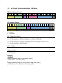
17. In-Crate Communication. PE-Bus.
PE-Bus Address Format
3 3 2 2 2 2 2 2 2 2 2 2 1 1 1 1 1 1 1 1 1 1 0 0 0 0 0 0 0 0 0 0
1 0 9 8 7 6 5 4 3 2 1 0 9 8 7 6 5 4 3 2 1 0 9 8 7 6 5 4 3 2 1 0
slot id
1..20, 31
channel
0..23, 31
z DS z page number
0 0..3 0
0…63
lower address
z z
0 0
PCI Address Format
2
3
2
2
2
1
2
0
1
9
1
8
slot id
1..20, 31
21
1
7
1
6
1
5
channel
0..23, 31
1
4
1
3
1
2
1
1
1
0
0
9
0
8
0
7
0
6
0
5
0
4
0
3
DS
lower address
0..3
see SLT specification
x – unused
z - for future
DS – Destination Select
00 - CFPGA Registers (global Registers, analog settings etc.)
01 - CFPGA Memory : iRAM (TestPattern, HitRate), SODIMM
10 - Periph. Registers ( Thresh, Settings, ADC-SPI settings, Statistics etc.)
11 - Periph. Memory ( QDR, iRAM)
lower address
10 bit + “00”
Channel address
0-23 select channel
31 all channels
Example:
long get_address (long slot, long base_addr) {
return (slot<<19 + base_addr) ;
}
long get_address (long slot, long channel, long base_addr) {
return (slot<<19 + channel<<14 + base_addr);
}
0
2
0
1
0
0
x
x
0
0
18. FLT Address Map
See KA_FLT_MemoryMap.pdf
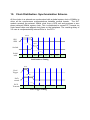
19. Clock Distribution. Synchronization Schema.
All the clocks in a subrack are synchronized with a global system clock of 20MHz to
allow all the synchronous communications between several boards. The SLT
module receives the external 10MHz clock from a GPS unit and produces a zero
phase delayed 20MHz system clock. This is distributed to several FLT boards via
clock fanout chips and aligned clock lines on the backplane. The resulting delay of
3.5 nsec is compensated by internal PLLs in the FLTs.
100 ns
GPS
1PPS
50 ns
SecStrb
RAM
addr
…
…
N-2
N-1
0
1
2
…
RAM Address Timing
50 ns
Pixel
Trigger
100 ns
PixTr
extend.
PixTr
Transmit
XXX
PT
Pixel Trigger Timing
XXX
XXX
20. Abbreviations
FD
PMT
FPGA
FLT
AB
SLT
JTAG
QDR
fluorescence detector
photomultiplier
field programmable gate array
first level trigger
analog board
second level trigger
joint test action group
quad data rate
21. References
SLTman
ADCds
PEbus
ABman
SLT user manual
ADC datasheet
Specification of PE-bus
Analog Board manual
22. Appendix A
23. 22.02.2012 Update: increase in bandwidth
Using SLT as data concentrator
SLT collects all triggers (energies + timestamp’s) in an EventFIFO Æ no ADC traces
Assumed a dead-time of 28*2 = 56 clock cycles Æ not working for shaping times < 2.8us.
SLT
N x FLT links
T
N
T
Ch01 FLT#i
R
T
Ch02 FLT#i
R
T
Ch24 FLT#i
…
ch# FLT#
SLT: Event FIFO
ch#
TS
E
…
ch#
R
TS
time
…
28bits
24 registers
FLTs
24bits/100ns
E
…
SLT
timer
R
pile-up
trigger info (energy + ???)
trigger bit
Readout
~120MB/s
120MB/s ~ 10MEvents/s ( 1Event = 12bytes) in energy mode.
Using SLT as status concentrator
SLT collects status of FLT’s fill pointers (FLT: EventFIFO) in Status/Interrupt Register.
SLT sends interrupt to DAQ-SW after programmable limit exceeded.
ISR delivers status of all FLT-FIFOs.
e.g.
fill_pointer_01 = 5; fill_pointer_02 = 0; fill_pointer_03 = 99;
…
fill_pointer_12 = 485;
…
fill_pointer_NN = 54;
DAQ_SW reads out corresponding FLTs.
??? 20MB/s ??? ~ 1-2MEvent/s in energy mode.
Using SLT as ‘readout master’
SLT analyzes FLT’s fill pointers, if necessary starts readout of FLTs immediate and finally
handles DMA transfer.
Reduced TimeStamp format
Split 32bit SecCounter in two one on SLT.
NEW: Filter and Trigger Update.
KATRIN trapezoidal filter is revised regarding better separation of peak pile-up effects as
recommended by Sanshiro (see his paper).
ADCdata
Z –(L)
Z -N
+
+
Z –(L)
-
-
1
1 − Z −1
+
+
1
1 − Z −1
X’ = (X *
coeff_x_128)
>>7;
X
+
coeff_x_128
Filter I
Z –L/2
Energy
Z –L/2
x2
+
> Thresh
-
+
+
+
+
Trigger
&
1
1 − Z −1
zero cross detector
Filter II
<0
1 – Z -1
Energy diff.
P2P
Z –1
Z –1
x2
+
+
+
Filter & Pixel Trigger
Implementation
1
1 − Z −1
Filter III
-
+
+
zero
cross
Flat-Top
counter
flat–top
length
stage I
stage II
stage III
Ediff
L = 128
E
TopLength
Filter & Pixel Timing Diagram
Trigger output consists of following data:
Parameter
Abbrev.
width in bits
Energy
E
20
Energy diff
Ediff
12 (normalized to ADC range)
flat-top length
TopLength 9
Timestamp
TimeStamp 48
Modes of operation
Several setting parameters control the behavior of daq and should be set in according to
desired operation mode.
Run FLT:EventFifo FLT:EventFifo traces/hist. SLT
Mode
Mode
length
behave
readout
readout
0
no
no
Standby
1
64
stop if full
yes
no
Trace Mode
1
512
overwrite
no
yes
Energy Mode
512
overwrite
no
yes
Extended Energy 5
overwrite
yes
no
Histogram Mode 2
3
?
?
?
?
Veto Mode
Parameter
Runmode
FLT:EventFifo length
FLT:EventFifo behave
bits
ControlReg[19:16]
ControlReg[25]
ControlReg[24]
description
0..3, 5
0 - 512, 1 -64
0 - overwrite, 1 – stop when full
default
0
0
0
NEW: Fast Events Readout for Energy Mode
Event information should be sent from FLT to SLT:
field
bit length
Trigger bit
1
Channels (Muliple)
5
Channel#
5
TimeStamp seconds lsb
12
TimeStamp subseconds
25+1 = 26
Energy
20
Energy diff.
12
Flat length
9
= 90 Æ 4 words a 23bit
description
FLT Æ SLT transmission format (PixLink):
10MHz clock
100 ns
23 bit payload
Start bit
Parity
one event transmission
…
word 1
word 2
word 3
word 4
word 1
word 2
word 3
next event
word 4
word 1
22 21 20 19 18 17 16 15 14 13 12 11 10 09 08 07 06 05 04 03 02 01 00
T
N (multipl.)
channel#
0 0 P
top length
Energy diff. normalized
Energy (20bit)
Energy (20bit)
TS_seconds (12bit)
TS_subseconds (25bit)
Time correction on SLT
if (FLT_TS_subseconds > SLT_subseconds)
TS_seconds = SLT_seconds – 1;
else
TS_seconds = SLT_seconds;
FLT Block Diagram
FIFO
depth 1K
trigger ch1
24
chan.
…
pixLink
???
MUX
92
trigger ch24
FLT
Timer
Event information stored on SLT:
field
bit length
Trigger bit
1
Channels (Muliple)
5
FLT#
5
Channel#
5
TimeStamp seconds msb
20
TimeStamp seconds lsb
12
TimeStamp subseconds
25+1 = 26
Energy
20
Energy diff.
12
Flat length
9
= 115 Æ 4 x 32bit
description
? time correction ?
? time correction ?
SLT Block Diagram
pixLink
Event FIFO
8MB
800MB/s
Chann. Energy
TS_seconds
TS_subseconds
ID Ediff. FlatL
Chann. Energy
TS seconds
TS subseconds
ID Ediff. FlatL
receiver
Nx
FLT
… …
???
MUX
receiver
20 x 3MB @ 10MHz
Æ 600MB/s
SLT
Second
Counter
Event
ID
Count
…
event
EventFIFO status
SLT Event FIFO contents: (see SLT description)
31
19
flt# (5bit) channel# (5bit)
p
mult. (5bit)
Event ID (11 bit)
16 15
0
Energy (20 bit)
TS seconds (32 bit)
TS subseconds (25 bit)
Energy diff. (12bit)
top length (9bit)
1 Event = 4 long = 16 byte
1 Event / 4*100 ns = 2.5MEvent /sec
FLT --> SLT transmission
22 21 20 19 18 17 16 15 14 13 12 11 10 09 08 07 06 05 04 03 02 01 00
word 1
T
N (multipl.)
channel#
0 0 P
top length
word 2
Energy diff. normalized
Energy (20bit)
word 3
Energy (20bit)
TS_seconds (12bit)
word 4
TS_subseconds (25bit)