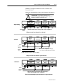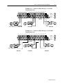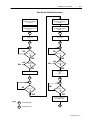
1
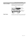
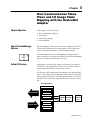
AllenBradley 8 Input RTD Module (Cat. No. 1794IR8) User Manual Important User Information Because of the variety of uses for the products described in this publication, those responsible for the application and use of this control equipment must satisfy themselves that all necessary steps have been taken to assure that each application and use meets all performance and safety requirements, including any applicable laws, regulations, codes and standards. The illustrations, charts, sample programs and layout examples shown in this guide are intended solely for example. Since there are many variables and requirements associated with any particular installation, Allen-Bradley does not assume responsibility or liability (to include intellectual property liability) for actual use based upon the examples shown in this publication. Allen-Bradley publication SGI–1.1, “Safety Guidelines For The Application, Installation and Maintenance of Solid State Control” (available from your local Allen-Bradley office) describes some important differences between solid-state equipment and electromechanical devices which should be taken into consideration when applying products such as those described in this publication. Reproduction of the contents of this copyrighted publication, in whole or in part, without written permission of Allen–Bradley Company, Inc. is prohibited. Throughout this manual we make notes to alert you to possible injury to people or damage to equipment under specific circumstances. ! ATTENTION: Identifies information about practices or circumstances that can lead to personal injury or death, property damage, or economic loss. Attention helps you: • identify a hazard • avoid the hazard • recognize the consequences Important: Identifies information that is especially important for successful application and understanding of the product. Important: We recommend you frequently backup your application programs on appropriate storage medium to avoid possible data loss. DeviceNet, DeviceNetManager, and RediSTATION are trademarks of Allen-Bradley Company, Inc. PLC, PLC–2, PLC–3, and PLC–5 are registered trademarks of Allen-Bradley Company, Inc. Windows is a trademark of Microsoft. Microsoft is a registered trademark of Microsoft IBM is a registered trademark of International Business Machines, Incorporated. All other brand and product names are trademarks or registered trademarks of their respective companies. Table of Contents Using This Manual . . . . . . . . . . . . . . . . . . . . . . . . . . . . . . . P-1 Preface Objectives . . . . . . . . . . . . . . . . . . . . . . . . . . . . . . . . . . . Audience . . . . . . . . . . . . . . . . . . . . . . . . . . . . . . . . . . . . . . . . . . Vocabulary . . . . . . . . . . . . . . . . . . . . . . . . . . . . . . . . . . . . . . . . What This Manual Contains . . . . . . . . . . . . . . . . . . . . . . . . . . . . Conventions . . . . . . . . . . . . . . . . . . . . . . . . . . . . . . . . . . . . . . . For Additional Information . . . . . . . . . . . . . . . . . . . . . . . . . . . . . . Summary . . . . . . . . . . . . . . . . . . . . . . . . . . . . . . . . . . . . . . . . . P-1 P-1 P-1 P-1 P-2 P-2 P-2 Overview of FLEX I/O and your RTD Module . . . . . . . . . . . 1-1 Chapter Objectives . . . . . . . . . . . . . . . . . . . . . . . . . . . . . . . . . . . The FLEX I/O System . . . . . . . . . . . . . . . . . . . . . . . . . . . . . . . . . How FLEX I/O RTD Modules Communicate with Programmable Controllers . . . . . . . . . . . . . . . . . . . . . . . . . . . Typical Communication Between an Adapter and a Module . . . . Features of your Modules . . . . . . . . . . . . . . . . . . . . . . . . . . . . . . Chapter Summary . . . . . . . . . . . . . . . . . . . . . . . . . . . . . . . . . . . 1-1 1-1 1-1 1-2 1-3 1-3 How to Install Your RTD Input Module . . . . . . . . . . . . . . . . 2-1 Before You Install Your Input Module . . . . . . . . . . . . . . . . . . . . . . European Union Directive Compliance . . . . . . . . . . . . . . . . . . . . . EMC Directive . . . . . . . . . . . . . . . . . . . . . . . . . . . . . . . . . . . . Low Voltage Directive . . . . . . . . . . . . . . . . . . . . . . . . . . . . . . . Power Requirements . . . . . . . . . . . . . . . . . . . . . . . . . . . . . . . . . Wiring the Terminal Base Units (1794TB2 and TB3 shown) . . . Installing the Module . . . . . . . . . . . . . . . . . . . . . . . . . . . . . . . . . . Connecting Wiring for the RTD Module . . . . . . . . . . . . . . . . . . . . Table 2.A Wiring connections for the 1794IR8 RTD Input Module . . . . . . Example of 2, 3 and 4wire RTD Wiring to a 1794TB3 Terminal Base Unit . . . . . . . . . . . . . . . . . . . . . . . . . . . . . . Example of 2, 3 and 4wire RTD Wiring to a 1794TB3T Terminal Base Unit . . . . . . . . . . . . . . . . . . . . . . . . . . . . . . Module Indicators . . . . . . . . . . . . . . . . . . . . . . . . . . . . . . . . . . . . Chapter Summary . . . . . . . . . . . . . . . . . . . . . . . . . . . . . . . . . . . 2-1 2-1 2-1 2-2 2-2 2-3 2-4 2-5 2-6 2-7 2-7 2-8 2-8 ii Table of Contents Module Programming . . . . . . . . . . . . . . . . . . . . . . . . . . . . 3-1 Chapter Objectives . . . . . . . . . . . . . . . . . . . . . . . . . . . . . . . . . . . Block Transfer Programming . . . . . . . . . . . . . . . . . . . . . . . . . . . . Sample programs for Flex I/O Analog Modules . . . . . . . . . . . . . . . PLC3 Programming . . . . . . . . . . . . . . . . . . . . . . . . . . . . . . . . . Figure 3.1 PLC3 Family Sample Program Structure . . . . . . . . . . . . . . . . PLC5 Programming . . . . . . . . . . . . . . . . . . . . . . . . . . . . . . . . . Figure 3.2 PLC5 Family Sample Program Structure . . . . . . . . . . . . . . . . PLC2 Programming . . . . . . . . . . . . . . . . . . . . . . . . . . . . . . . . . Chapter Summary . . . . . . . . . . . . . . . . . . . . . . . . . . . . . . . . . . . 3-1 3-1 3-2 3-2 3-2 3-3 3-3 3-3 3-3 Writing Configuration to and Reading Status from Your Module with a Remote I/O Adapter . . . . . . . . . . . 4-1 Chapter Objectives . . . . . . . . . . . . . . . . . . . . . . . . . . . . . . . . . . . Configuring Your RTD Module . . . . . . . . . . . . . . . . . . . . . . . . . . . Range Selection . . . . . . . . . . . . . . . . . . . . . . . . . . . . . . . . . . . . Input Scaling . . . . . . . . . . . . . . . . . . . . . . . . . . . . . . . . . . . . . . . Enhanced Mode . . . . . . . . . . . . . . . . . . . . . . . . . . . . . . . . . . . . Hardware First Notch Filter . . . . . . . . . . . . . . . . . . . . . . . . . . . . . Throughput in Normal Mode . . . . . . . . . . . . . . . . . . . . . . . . . . Throughput in Enhanced Mode . . . . . . . . . . . . . . . . . . . . . . . . Reading Data From Your Module . . . . . . . . . . . . . . . . . . . . . . . . . Mapping Data for the Analog Modules . . . . . . . . . . . . . . . . . . . . . RTD Input Module (1794IR8) Image Table Mapping . . . . . . . . . RTD Analog Input Module (1794IR8) Read Words . . . . . . . . . . RTD Analog Input Module (1794IR8) Write Words . . . . . . . . . . Word/Bit Descriptions for the 1794IR8 RTD Analog Input Module Chapter Summary . . . . . . . . . . . . . . . . . . . . . . . . . . . . . . . . . . . 4-1 4-1 4-2 4-2 4-3 4-4 4-4 4-4 4-4 4-5 4-5 4-5 4-6 4-6 4-8 How Communication Takes Place and I/O Image Table Mapping with the DeviceNet Adapter . . . . . . . . . 5-1 Chapter Objectives . . . . . . . . . . . . . . . . . . . . . . . . . . . . . . . . . . . About DeviceNetManager Software . . . . . . . . . . . . . . . . . . . . . . . Polled I/O Structure . . . . . . . . . . . . . . . . . . . . . . . . . . . . . . . . . . Adapter Input Status Word . . . . . . . . . . . . . . . . . . . . . . . . . . . System Throughput . . . . . . . . . . . . . . . . . . . . . . . . . . . . . . . . . . Mapping Data into the Image Table . . . . . . . . . . . . . . . . . . . . . . . RTD Input Analog Module (1794IR8) Image Table Mapping . . . Memory Map of RTD Analog Input Module Image Table - 1794IR8 . . . . . . . . . . . . . . . . . . . . . . . . . . Word/Bit Descriptions for the 1794IR8 RTD Analog Input Module . . . . . . . . . . . . . . . . . . . . . . . . . . . . . . . . . . Defaults . . . . . . . . . . . . . . . . . . . . . . . . . . . . . . . . . . . . . . . . . . 5-1 5-1 5-1 5-2 5-3 5-3 5-3 5-4 5-4 5-7 Table of Contents iii Calibrating Your Module . . . . . . . . . . . . . . . . . . . . . . . . . . 6-1 Chapter Objective . . . . . . . . . . . . . . . . . . . . . . . . . . . . . . . . . . . When and How to Calibrate Your RTD Module . . . . . . . . . . . . . . . Tools and Equipment . . . . . . . . . . . . . . . . . . . . . . . . . . . . . . . . . Manually Calibrating your RTD Input Module . . . . . . . . . . . . . . . . Flow Chart for Calibration Procedure . . . . . . . . . . . . . . . . . . . . Calibration Setups . . . . . . . . . . . . . . . . . . . . . . . . . . . . . . . . . Wiring Connections for the RTD Module . . . . . . . . . . . . . . . . . . Read/Write Words for Calibration . . . . . . . . . . . . . . . . . . . . . . . Offset Calibration . . . . . . . . . . . . . . . . . . . . . . . . . . . . . . . . . . Gain Calibration . . . . . . . . . . . . . . . . . . . . . . . . . . . . . . . . . . . Table 6.A Calibration Resistance/Voltage Values for the 1794IR8 . Calibrating Your RTD Module using DeviceNet Manager Software (Cat. No. 1787MGR) . . . . . . . . . . . . . . . . . . . . . . . Offset Calibration . . . . . . . . . . . . . . . . . . . . . . . . . . . . . . . . . . Gain Calibration . . . . . . . . . . . . . . . . . . . . . . . . . . . . . . . . . . . 6-1 6-1 6-1 6-2 6-3 6-4 6-4 6-4 6-5 6-6 6-6 6-7 6-7 6-10 Specifications . . . . . . . . . . . . . . . . . . . . . . . . . . . . . . . . . . A-1 RTD Accuracy at Worst Case . . . . . . . . . . . . . . . . . . . . . . . . . . . Derating Curve . . . . . . . . . . . . . . . . . . . . . . . . . . . . . . . . . . . . . Support Services . . . . . . . . . . . . . . . . . . . . . . . . . . . . . . . . . . . . Technical Support . . . . . . . . . . . . . . . . . . . . . . . . . . . . . . . . . Engineering and Field Services . . . . . . . . . . . . . . . . . . . . . . . . Technical Training . . . . . . . . . . . . . . . . . . . . . . . . . . . . . . . . . Repair and Exchange Services . . . . . . . . . . . . . . . . . . . . . . . . A-3 A-3 6-1 6-1 6-1 6-1 6-1 Preface Using This Manual Preface Objectives Read this preface to familiarize yourself with this manual and to learn how to use it properly and efficiently. Audience We assume that you have previously used an Allen-Bradley programmable controller, that you are familiar with its features, and that you are familiar with the terminology we use. If not, read the user manual for your processor before reading this manual. In addition, if using this module in a DeviceNet system, you must be familiar with: • DeviceNetManager Software, cat. no. 1787-MGR • Microsoft Windows Vocabulary In this manual, we refer to: • the individual RTD module as the “module.” • the programmable controller as the “controller” or the “processor.” What This Manual Contains The contents of this manual are as follows: Chapter Title What's Covered 1 Overview of Flex I/O and Your RTD Module Describes features, capabilities, and hardware components 2 How to Install Your RTD Input Module Installation and connecting wiring 3 Module Programming Block transfer programming and programming examples 4 Writing Configuration to and Reading Status from Your Module with a Remote I/O Adapter Describes block transfer write and block transfer read configurations, including complete bit/word descriptions 5 How Communication Takes Place and I/O Image Table Mapping with the DeviceNet Adapter Describes communication over the I/O backplane between the module and the adapter, and how data is mapped into the image table 6 Calibrating Your Module Lists the tools needed, and the methods used to calibrate the RTD input module Specifications Module specifications, accuracy and derating curve Appendix A Publication 17946.5.4 P–2 Using This Manual Conventions We use these conventions in this manual: In this manual, we show: Like this: that there is more information about a topic in another chapter in this manual that there is more information about the topic in another manual For Additional Information For additional information on FLEX I/O systems and modules, refer to the following documents: Catalog Number 1787MGR Publication 17946.5.4 Publications Description Installation Instructions DeviceNetManager Software User Manual User Manual 17876.5.3 Industrial Automation Wiring and Grounding Guidelines for Noise Immunity 17704.1 1794 FLEX I/O Product Data 17942.1 1794ADN DeviceNet Adapter 17945.14 17946.5.5 1794ASB Remote I/O Adapter 17945.11 17946.5.3 1794 Summary More This preface gave you information on how to use this manual efficiently. The next chapter introduces you to the RTD module. Chapter 1 Overview of FLEX I/O and your RTD Module Chapter Objectives In this chapter, we tell you about: • what the FLEX I/O system is and what it contains • how FLEX I/O modules communicate with programmable controllers • the features of your RTD module The FLEX I/O System Adapter/Power Supply FLEX I/O is a small, modular I/O system for distributed applications that performs all of the functions of rack-based I/O. The FLEX I/O system contains the following components shown below: Terminal Base RTD Input Module 20125 • adapter/power supply – powers the internal logic for as many as eight I/O modules • terminal base – contains a terminal strip to terminate wiring for two- or three-wire devices • I/O module – contains the bus interface and circuitry needed to perform specific functions related to your application How FLEX I/O RTD Modules Communicate with Programmable Controllers FLEX I/O RTD modules are block transfer modules that interface analog signals with any Allen-Bradley programmable controllers that have block transfer capability. Block transfer programming moves input or output data words between the module’s memory and a designated area in the processor data table. Block transfer programming also moves configuration words from the processor data table to module memory. Publication 17946.5.4 1-2 Overview of FLEX I/O and your RTD Module The adapter/power supply transfers data to the module (block transfer write) and from the module (block transfer read) using BTW and BTR instructions in your ladder diagram program. These instructions let: • the adapter obtain input or output values and status from the module • you establish the module’s mode of operation. The illustration describes the communication process. Typical Communication Between an Adapter and a Module 1 2 The adapter transfers your configuration data to the module using a BTW. External devices transmit analog signals to the module. Flexbus AllenBradley AllenBradley ADAPTER ACTIVE FAULT LOCAL FAULT 3 WIRE RTD INPUT 8 CHANNEL 24VDC POWER SUPPLY RIO ADAPTER 1794ASB 4 Your ladder program instructs the adapter to perform a BTR of the values and stores them in a data table. 3 INPUT 0_ INPUT 1 _ INPUT 2_ INPUT 3_ INPUT 4 _ INPUT 5 _ INPUT 6 _ INPUT 7_ OK + + + + + + + + 5 The adapter and module determine that the transfer was made without error and input values are within specified range. 6 Your ladder program can use and/or move the data (if valid) before it is written over by the transfer of new data in a subsequent transfer. 7 Your ladder program performs BTWs to the module only when you power it up, or any time you wish to reconfigure the module. Publication 17946.5.4 1794-IR8 3 The module converts analog signals into binary format and stores these values until the adapter requests their transfer. Overview of FLEX I/O and your RTD Module Features of your Modules 1-3 The module label identifies the keyswitch position, wiring and module type. A removable label provides space for writing individual designations per your application. An indicator is provided to show when power is applied to the module. 1794IR8 Module Type AllenBradley 3WIRE RTD INPUT 8 CHANNEL Removable Label 1794IR8 3 INPUT 0 INPUT 1 INPUT 2 INPUT 3 INPUT 4 INPUT 5 INPUT 6 INPUT 7 + _ + _ + _ + _ + _ + _ + _ + _ OK Keyswitch Position Indicator (#3) Power On Indicator Input Designators Chapter Summary In this chapter, we told you about the FLEX I/O system and the RTD module, and how they communicate with programmable controllers. Publication 17946.5.4 Chapter 2 How to Install Your RTD Input Module In this chapter, we tell you: • • • • Before You Install Your Input Module how to install your module how to set the module keyswitch how to wire the terminal base about the indicators Before installing your analog module in the I/O chassis: You need to: As described under: Calculate the power requirements of all modules in each chassis. Power Requirements, page 22 Position the keyswitch on the terminal base Installing the Module, page 2-4 ! European Union Directive Compliance ATTENTION: The RTD module does not receive power from the backplane. +24V dc power must be applied to your module before installation. If power is not applied, the module position will appear to the adapter as an empty slot in your chassis. If this product has the CE mark it is approved for installation within the European Union and EEA regions. It has been designed and tested to meet the following directives. EMC Directive This product is tested to meet Council Directive 89/336/EEC Electromagnetic Compatibility (EMC) and the following standards, in whole or in part, documented in a technical construction file: • EN 50081-2EMC – Generic Emission Standard, Part 2 – Industrial Environment • EN 50082-2EMC – Generic Immunity Standard, Part 2 – Industrial Environment This product is intended for use in an industrial environment. Publication 17946.5.4 2–2 How to Install Your RTD Input Module Low Voltage Directive This product is tested to meet Council Directive 73/23/EEC Low Voltage, by applying the safety requirements of EN 61131–2 Programmable Controllers, Part 2 – Equipment Requirements and Tests. For specific information required by EN 61131-2, see the appropriate sections in this publication, as well as the following Allen-Bradley publications: • Industrial Automation Wiring and Grounding Guidelines For Noise Immunity, publication 1770-4.1 • Guidelines for Handling Lithium Batteries, publication AG-5.4 • Automation Systems Catalog, publication B111 Power Requirements The wiring of the terminal base unit is determined by the current draw through the terminal base. Make certain that the current draw does not exceed 10A. ! Publication 17946.5.4 ATTENTION: Total current draw through the terminal base unit is limited to 10A. Separate power connections may be necessary. How to Install Your RTD Input Module 2–3 Methods of wiring the terminal base units are shown in the illustration below. Wiring the Terminal Base Units (1794-TB2 and -TB3 shown) ! ATTENTION: Do not daisy chain power or ground from the RTD terminal base unit to any ac or dc discrete module terminal base unit. RTD or Analog Module Daisychaining 24V dc RTD or Analog Module RTD or Analog Module RTD or Analog Module Note: All modules must be analog modules for this configuration. Wiring when total current draw is less than 10A Discrete Module Individual RTD Module Discrete Module Discrete Module 24V dc 24V dc or 120V ac Note: Use this configuration if using any noisy" dc discrete I/O modules in your system. 24V dc or 120V ac RTD Module wiring separate from discrete wiring. Wiring when total current draw is greater than 10A Discrete Module Combination RTD or Analog Module RTD or Analog Module RTD or Analog Module 24V dc 24V dc or 120V ac Note: All modules powered by the same power supply must be analog modules for this configuration. Total current draw through any base unit must not be greater than 10A Publication 17946.5.4 2–4 How to Install Your RTD Input Module Installing the Module The RTD analog module mounts on a 1794-TB2, -TB3 or TB3T terminal base unit. 7 3 1 2 6 4 5 1. Rotate the keyswitch (1) on the terminal base unit (2) clockwise to position 3. 2. Make certain the flexbus connector (3) is pushed all the way to the left to connect with the neighboring terminal base/adapter. You cannot install the module unless the connector is fully extended. ! ATTENTION: Remove field-side power before removing or inserting the module. This module is designed so you can remove and insert it under backplane power. When you remove or insert a module with field-side power applied, an electrical arc may occur. An electrical arc can cause personal injury or property damage by: • sending an erroneous signal to your system’s field devices causing unintended machine motion • causing an explosion in a hazardous environment Repeated electrical arcing causes excessive wear to contacts on both the module and its mating connector. Worn contacts may create electrical resistance. 3. Before installing the module, check to make sure that the pins on the bottom of the module are straight so they will align properly with the female connector in the terminal base unit. 4. Position the module (4) with its alignment bar (5) aligned with the groove (6) on the terminal base. 5. Press firmly and evenly to seat the module in the terminal base unit. The module is seated when the latching mechanism (7) is locked into the module. 6. Repeat the above steps to install the next module in its terminal base unit. Publication 17946.5.4 How to Install Your RTD Input Module Connecting Wiring for the RTD Module 2–5 Wiring to the RTD module is made through the terminal base unit on which the module mounts. Compatible terminal base unit are: 1 Module 1794TB2 1794TB3 1794TB3T1 1794IR8 Yes Yes Yes The 1794TB3T terminal base unit contains cold junction compensation for use with thermocouple modules. 1794TB2 and 1794TB3 0 1 2 3 4 5 6 7 1794TB3T 8 9 10 11 12 13 14 15 COM COM V V A 0 -15 A B 16-33 B C 34-51 C 0 1 2 3 4 5 6 7 8 9 10 11 12 13 14 15 C C N0 C N1 C N2 C N3 C N4 C N5 C N6 C N7 C V C J C Where: V = 24V dc C = 24V dc common CJC = cold junction compensation These terminals on 1794TB3 only. V = 24V dc COM = 24V dc common C J C V N = additional input = chassis ground Connecting Wiring using a 1794TB2, TB3 and TB3T Terminal Base Units 1. Connect the individual signal wiring to numbered terminals on the 0–15 row (A) on the terminal base unit. Connect the high side to the even numbered terminals, and the low side to the odd numbered terminals. See Table 2.A. 2. Connect channel common to the associated signal return terminal on row B, as shown in Table 2.A. 3. Terminate shields: • On 1794-TB2 and -TB3 bases only: terminate shields to the associated shield return terminals on row (B). • On 1794-TB3T bases only: terminate shields to terminals 39 to 46 on row C. Important: 1794-TB2 and -TB3 terminal base units have row (B) bussed together. When you terminate your shields to this row, the shields will be at the same potential as the power supply return. 4. Connect +24V dc to terminal 34 on the 34-51 row (C), and 24V common to terminal 16 on the B row. Important: To reduce susceptibility to noise, power analog modules and discrete modules from separate power supplies. Publication 17946.5.4 2–6 How to Install Your RTD Input Module 5. If daisy chaining the +24V dc power to the next base unit, connect a jumper from terminal 51 on this base unit to terminal 34 on the next base unit. ATTENTION: Do not daisy chain power or ground from the RTD terminal base unit to any ac or dc discrete module terminal base unit. ! ATTENTION: The RTD modules do not receive power from the backplane. +24V dc power must be applied to your module before operation. If power is not applied, the module position will appear to the adapter as an empty slot in your chassis. If the adapter does not recognize your module after installation is completed, cycle power to the adapter. ! Table 2.A Wiring connections for the 1794IR8 RTD Input Module RTD Channel 1 1794TB2 and TB3 Terminal Base Units 1794TB3T Terminal Base Unit High Signal Terminal Low Signal Terminal Signal Return1 Shield Return High Signal Terminal Low Signal Terminal Signal Return1 Shield Return2 0 0 1 17 18 0 1 17 39 1 2 3 19 20 2 3 19 40 2 4 5 21 22 4 5 21 41 3 6 7 23 24 6 7 23 42 4 8 9 25 26 8 9 25 43 5 10 11 27 28 10 11 27 44 6 12 13 29 30 12 13 29 45 7 14 15 31 32 14 15 31 46 24V dc Common 16 thru 33 16, 17, 19, 21, 23, 25, 27, 29, 31 and 33 +24V dc power 1794TB2 - 34 and 51 1794TB3 - 34 thru 51 34, 35, 50 and 51 When using a 2wire RTD, jumper the signal return to the low signal terminal. ! Publication 17946.5.4 2 Terminals 39 to 46 are chassis ground. ATTENTION: Total current draw through the terminal base unit is limited to 10A. Separate power connections to the terminal base unit may be necessary. How to Install Your RTD Input Module 2–7 Example of 2-, 3- and 4-wire RTD Wiring to a 1794-TB3 Terminal Base Unit 0 1 0 1 17 16 3 3 18 35 34 2 2 19 36 4 4 20 37 5 6 5 21 38 6 22 39 7 8 7 23 40 8 24 41 9 9 25 42 10 10 26 43 11 11 27 44 12 12 28 45 13 13 29 46 14 14 30 47 15 15 31 48 32 49 33 50 51 0 -15 A 16-33 B 34-51 C 1794TB3 Clip or tieback 4th lead. 4Wire RTD 3Wire RTD 2Wire RTD Example of 2-, 3- and 4-wire RTD Wiring to a 1794-TB3T Terminal Base Unit 0 1 0 1 17 16 34 2 2 18 35 3 3 19 36 4 4 20 37 5 21 38 6 5 6 22 39 7 23 40 8 7 8 24 41 9 9 25 42 10 10 26 43 11 11 27 44 12 12 28 45 13 13 29 46 14 14 30 47 15 15 31 48 32 49 33 50 51 0 -15 A 16-33 B 34-51 C 1794TB3T Clip or tieback 4th lead. 4Wire RTD 3Wire RTD 2Wire RTD Publication 17946.5.4 2–8 How to Install Your RTD Input Module Module Indicators The RTD module has one status indicator that is on when power is applied to the module. This indicator has 3 different states: AllenBradley 1794-IR8 3 WIRE RTD INPUT 8 CHANNEL 3 INPUT 0_ INPUT 1 _ INPUT 2_ INPUT 3_ INPUT 4 _ INPUT 5 _ INPUT 6 _ INPUT 7_ + + + + + + + + B OK A A = Status Indicator - indicates diagnostic results and configuration status B = Insertable label for writing individual input designations Color Red Green Chapter Summary Publication 17946.5.4 State Meaning On Indicates a critical fault (diagnostic failure, etc.) Blinking Indicates a noncritical fault (such as open sensor, input out of range, etc.) On Module is configured and fully operational Blinking Module is functional but not configured Off Module not powered In this chapter, we told you how to install your input module in an existing programmable controller system and how to wire to the terminal base units. Chapter 3 Module Programming Chapter Objectives In this chapter, we tell you about: • block transfer programming • sample programs for the PLC-3 and PLC-5 processors Block Transfer Programming Your module communicates with the processor through bidirectional block transfers. This is the sequential operation of both read and write block transfer instructions. A configuration block transfer write (BTW) is initiated when the RTD module is first powered up, and subsequently only when the programmer wants to enable or disable features of the module. The configuration BTW sets the bits which enable the programmable features of the module, such as scaling, alarms, ranges, etc. Block transfer reads are performed to retrieve information from the module. Block transfer read (BTR) programming moves status and data from the module to the processor’s data table. The processor user program initiates the request to transfer data from the module to the processor. The transferred words contain module status, channel status and input data from the module. ! ATTENTION: If the RTD module is not powered up before the remote I/O adapter, the adapter will not recognize the module. Make certain that the RTD module is installed and powered before or simultaneously with the remote I/O adapter. If the adapter does not establish communication with the module, cycle power to the adapter. The following sample programs are minimum programs; all rungs and conditioning must be included in your application program. You can disable BTRs, or add interlocks to prevent writes if desired. Do not eliminate any storage bits or interlocks included in the sample programs. If interlocks are removed, the program may not work properly. Your program should monitor status bits and block transfer read activity. Publication 17946.5.4 3–2 Module Programming Sample programs for Flex I/O Analog Modules The following sample programs show you how to use your analog module efficiently when operating with a programmable controller. These programs show you how to: • configure the module • read data from the module • update the module’s output channels (if used) These programs illustrate the minimum programming required for communication to take place. PLC3 Programming Block transfer instructions with the PLC-3 processor use one binary file in a data table section for module location and other related data. This is the block transfer control file. The block transfer data file stores data that you want transferred to your module (when programming a block transfer write) or from your module (when programming a block transfer read). The address of the block transfer data files are stored in the block transfer control file. The same block transfer control file is used for both the read and write instructions for your module. A different block transfer control file is required for every module. A sample program segment with block transfer instructions is shown in Figure 3.1, and described below. Figure 3.1 PLC3 Family Sample Program Structure Enable BTR Program Action At powerup,in RUN mode, or when the processor is switched from PROG to RUN, the user program enables a block transfer read. Then it initiates a block transfer write to configure the module. 1 15 The pushbutton allows the user to manually request a block transfer write. Publication 17946.5.4 7 0 0 #B3:0 #B4:0 11 EN 12 Done DN 15 Error ER 13 Thereafter, the program continuously performs read block transfers. Note: You must create the data file for the block transfers before you enter the block transfer instructions. Block Transfer Read Done Bit B3:0 BLOCK XFER READ RACK: GROUP: MODULE: CONTROL: DATA FILE: LENGTH: Pushbutton 2 Block Transfer Write Done Bit B3:0 05 Powerup Bit B4:10 03 Enable BTW BLOCK XFER WRITE RACK: GROUP: MODULE: CONTROL: DATA FILE: LENGTH: 7 0 0 #B3:0 #B5:0 3 EN 02 Done DN 05 Error ER 03 Module Programming 3–3 PLC5 Programming The PLC-5 program is very similar to the PLC-3 program with the following exceptions: • block transfer enable bits are used instead of done bits as the conditions on each rung. • separate block transfer control files are used for the block transfer instructions. Figure 3.2 PLC5 Family Sample Program Structure Program Action 1 BTR Enable Bit N12:0 Thereafter, the program continuously per forms read block transfers. Pushbutton 2 2 1 0 N12:0 N13:0 11 N RACK: GROUP: MODULE: CONTROL: DATA FILE: LENGTH: CONTINUOUS: 15 At powerup,in RUN mode, or when the processor is switched from PROG to RUN, the user program enables a block transfer read. Then it initiates a block transfer write to configure the module. The pushbutton allows the user to manually request a block transfer write. BTR BLOCK TRANSFER READ BTW Enable Bit N12:5 15 Powerup Bit N13:10 03 BTW BLOCK TRANSFER WRITE RACK: GROUP: MODULE: CONTROL: DATA FILE: LENGTH: CONTINUOUS: 2 1 0 N12:5 N13:20 3 N EN DN ER EN DN ER PLC2 Programming The 1794 analog I/O modules are not recommended for use with PLC-2 family programmable controllers due to the number of digits needed for high resolution. Chapter Summary In this chapter, we told you how to program your programmable controller. You were given sample programs for your PLC-3 and PLC-5 family processors. Publication 17946.5.4 Chapter 4 Writing Configuration to and Reading Status from Your Module with a Remote I/O Adapter Chapter Objectives In this chapter, we tell you how: • • • • Configuring Your RTD Module to configure your module’s features to enter your data to read data from your module about the read block format The RTD module is configured using a group of data table words that are transferred to the module using a block transfer write instruction. The software configurable features available are: • • • • input/output range selection, including full range and bipolar selectable first notch filter data reported in oF, oC, unipolar or bipolar count enhanced mode Note: PLC-5 family programmable controllers that use 6200 software programming tools can take advantage of the IOCONFIG utility to configure these modules. IOCONFIG uses menu-based screens for configuration without having to set individual bits in particular locations. Refer to your 6200 software literature for details. Publication 17946.5.4 4–2 Writing Configuration to and Reading Status from Your Module with a Remote I/O Adapter Range Selection Individual input channels are configurable to operate with the following sensor types: Input Signal Range Resistance 1 to 433Ω RTD Input Signal Range Alpha = Degrees 100 ohm Pt (Euro) 0.00385 -200 to +870oC 100 ohm Pt (U.S.) 0.003916 -200 to +630oC 200 ohm Pt 0.00385 -200 to +630oC 500 ohm Pt 0.00385 -200 to +630oC 100 ohm Nickel 0.00618 -60 to +250oC 120 ohm Nickel 0.00672 -80 to +290oC 200 ohm Nickel 0.00618 -60 to +250oC 500 ohm Nickel 0.00618 -60 to +250oC 10 ohm Copper 0.00427 -200 to +260oC You select individual channel ranges using write words 1 and 2 of the block transfer write instruction. Input Scaling Scaling lets you report each channel in actual engineering units. Scaled values are in integer format. Range Degrees +1 to 433Ω Maximum Resolution 10 to 4330 100mΩ 100 ohm Pt Euro -200 to +870oC -2000 to +8700 0.1oC 100 ohm Pt U.S -200 to +630oC -2000 to +6300 0.1oC 200 ohm Pt Euro -200 to +630oC -2000 to +6300 0.1oC 500 ohm Pt Euro -200 to +630oC -2000 to +6300 0.1oC 100 ohm Nickel -60 to +250oC -600 to +2500 0.1oC 120 ohm Nickel -80 to +290oC -800 to +2900 0.1oC 200 ohm Nickel -60 to +250oC -600 to +2500 0.1oC 500 ohm Nickel -60 to +250oC -600 to +2500 0.1oC 10 ohm Copper -200 to +260oC -2000 to +26000 0.1oC Continued on next page Publication 17946.5.4 Counts Writing Configuration to and Reading Status from Your Module with a Remote I/O Adapter Counts 4–3 Maximum Resolution Range Degrees 100 ohm Pt Euro -328 to +1598oF -3280 to +15980 0.1oF 100 ohm Pt U.S -328 to +1166oF -3280 to +11660 0.1oF 200 ohm Pt Euro -328 to +1166oF -3280 to +11660 0.1oF 500 ohm Pt Euro -328 to +1166oF -3280 to +11660 0.1oF 100 ohm Nickel -76 to +482oF -760 to +4820 0.1oF 120 ohm Nickel -112 to +500oF -1120 to +5000 0.1oF 200 ohm Nickel -76 to +482oF -760 to +4820 0.1oF 500 ohm Nickel -76 to +482oF -760 to +4820 0.1oF 10 ohm Copper -328 to +500oF -3280 to +5000 0.1oF Note: Temperature data has an implied decimal point 1 space to the right of the last digit. (divide by 10). For example, a readout of 1779o would actually be 177.9o. You select input scaling using the designated words of the write block transfer instruction. Refer to the Bit/Word description for write word 0, bits 00 and 01. Enhanced Mode You can select an enhanced mode of operation for this module. The enhanced mode lets you determine the value of an unknown RTD input. The voltage drop across a precision resistor in the module is taken once each sensor scan, and compared to the unknown input. The result is used to determine the value of the unknown RTD. This results in improved module temperature drift characteristics and accuracy. However, since the comparision is done each program scan, the result is decreased module throughput. Publication 17946.5.4 4–4 Writing Configuration to and Reading Status from Your Module with a Remote I/O Adapter Hardware First Notch Filter A hardware filter in the analog to digital converter lets you select a frequency for the first notch of the filter. Selection of the filter influences the analog to digital output data rate and changes the module throughput. Module throughput is a function of the number of inputs used and the first notch filter. Both of these influence the time from an RTD input to arrival at the flexbus backplane. Throughput in Normal Mode A/D Filter First Notch Frequency (effective resolution) 10Hz (16bits) 25Hz (16bits) 50Hz (16bits) Number of channels scanned 1 60Hz (16bits) 100Hz (16bits) 250Hz (13bits) 500Hz (11bits) 1000Hz (9bits) System Throughput (in ms or s) 1 325 145 85 75 55 37 31 28 2 650 290 170 150 110 74 62 56 3 975 435 255 225 165 111 93 84 4 1.3s 580 340 300 220 148 124 112 5 1.625s 725 425 375 275 185 155 140 6 1.95s 870 510 450 330 222 186 168 7 2.275s 1.015s 595 525 385 259 217 196 8 2.60s1 1.16s 680 600 440 296 248 224 250Hz (16bits) 500Hz (11bits) 1000Hz (9bits) Default setting Throughput in Enhanced Mode A/D Filter First Notch Frequency (effective resolution) 10Hz (16bits) 25Hz (16bits) 50Hz (16bits) Number of channels scanned 1 60Hz (16bits) 100Hz (16bits) System Throughput (in ms or s) 1 650 290 170 150 110 74 62 56 2 975 435 255 225 165 111 93 84 3 1.3s 580 340 300 220 148 124 112 4 1.625s 725 425 375 275 185 155 140 5 1.95s 870 510 450 330 222 186 168 6 2.275s 1.015s 595 525 385 259 217 196 7 2.60s 1.16s 680 600 440 296 248 224 8 2.925s1 1.305s 765 675 495 333 279 252 Default setting Reading Data From Your Module Publication 17946.5.4 Read programming moves status and data from the RTD input module to the processor’s data table in one I/O scan. The processor’s user program initiates the request to transfer data from the RTD input module to the processor. Writing Configuration to and Reading Status from Your Module with a Remote I/O Adapter Mapping Data for the Analog Modules 4–5 The following read and write words and bit/word descriptions describe the information written to and read from the RTD input module. The module uses up to 11 words of input data and up to 4 words of output data. Each word is composed of 16 bits. RTD Input Module (1794IR8) Image Table Mapping Module Image Reserved Input Data Channel 0 Input Data Channel 1 I/O Image Input Data Channel 2 Input Size Input Data Channel 3 1 to 11 Words Input Data Channel 4 Input Data Channel 5 Input Data Channel 6 Input Data Channel 7 Overrange Underrange Calibration Status Output Size Configuration Calibration Mask 0 to 3 Words RTD Type RTD Type RTD Analog Input Module (1794-IR8) Read Words Decimal Bit 15 14 13 12 11 10 09 08 07 06 05 04 03 02 01 00 Octal Bit 17 16 15 14 13 12 11 10 07 06 05 04 03 02 01 00 Reserved 0 0 Word 0 Reserved 1 Channel 0 Input Data 2 Channel 1 Input Data 3 Channel 2 Input Data 4 Channel 3 Input Data 5 Channel 4 Input Data 6 Channel 5 Input Data 7 Channel 6 Input Data 8 Channel 7 Input Data 9 10 Overrange Bits 0 0 0 0 0 Bad Cal Underrange Bits Cal Done Cal Range 0 Diagnostic Status Bits Pwr Up Publication 17946.5.4 4–6 Writing Configuration to and Reading Status from Your Module with a Remote I/O Adapter RTD Analog Input Module (1794-IR8) Write Words Decimal Bit 15 14 13 12 11 10 09 08 07 06 05 04 03 02 01 00 Octal Bit 17 16 15 14 13 12 11 10 07 06 05 04 03 02 01 00 Cal Clk Cal Hi Cal Lo Word 0 8bit Calibration Mask Filter Cutoff Enh MDT 1 RTD 3 Type RTD 2 Type RTD 1 Type RTD 0 Type 2 RTD 7 Type RTD 6 Type RTD 5 Type RTD 4 Type Where: Enh = Enhanced MDT = Module Data Type Word/Bit Descriptions for the 1794-IR8 RTD Analog Input Module Word Dec. Bits (Octal Bits) Description Read Word 0 00-15 (00-17) Reserved Read Word 1 00-15 (00-17) Channel 0 Input data Read Word 2 00-15 (00-17) Channel 1 Input data Read Word 3 00-15 (00-17) Channel 2 Input data Read Word 4 00-15 (00-17) Channel 3 Input data Read Word 5 00-15 (00-17) Channel 4 Input data Read Word 6 00-15 (00-17) Channel 5 Input data Read Word 7 00-15 (00-17) Channel 6 Input data Read Word 8 00-15 (00-17) Channel 7 Input data Read Word 9 00-07 08-15 (10-17) 00-01 Read Word 10 Overrange bits - these bits are set if 1), the input signal is above the input channel's maximum range, or 2), an open detector is detected. Not used - set to 0 02 Reserved 03 Powerup bit - this bit is set (1) until configuration data is received by the module. 04-06 07 Critical Error bits - If these bits are anything other than all zeroes, return the module to the factory for repair Unused - set to 0 08 (10) Calibration Range bit - set to 1 if a reference signal is out of range during calibration 09 (11) Calibration Done bit - set to 1 after an initiated calibration cycle is complete. 10 (12) Calibration Bad bit - set to 1 if the channel has not had a valid calibration. 11-15 (13-17) Publication 17946.5.4 Underrange bits - these bits are set if the input signal is below the input channel's minimum range. Unused - set to 0 Writing Configuration to and Reading Status from Your Module with a Remote I/O Adapter Word Write word 0 Dec. Bits (Octal Bits) 00-01 Description Module Data Type Bit 02 03-05 01 00 0 0 oC 0 1 oF 1 0 Bipolar counts scaled between -32768 and +32767 1 1 Unipolar counts scaled between 0 and 65535 (default) Enhanced mode select - measures voltage drop across a precision resistor in the module to compare with the unknown input. This improves module temperature drift characteristics, but reduces module throughput. A/D Filter First Notch Frequency Bit 05 04 03 Definition 0 0 0 10Hz (default) 0 0 1 25Hz 0 1 0 50Hz 0 1 1 60Hz 1 0 0 100Hz 1 0 1 250Hz 1 1 0 500Hz 1 1 1 1000Hz 06 Calibration High/Low bit - This bit is set during gain calibration; reset during offset calibration. 07 Calibration clock - this bit must be set to 1 to prepare for a calibration cycle; then reset to 0 to initiate calibration. 08-15 (10-17) 4–7 Calibration mask - The channel, or channels, to be calibrated will have the correct mask bit set. Bit 8 corresponds to channel 0, bit 9 to channel 1, and so on. Publication 17946.5.4 4–8 Word Writing Configuration to and Reading Status from Your Module with a Remote I/O Adapter Dec. Bits (Octal Bits) Write Word 1 00-03 Description Channel 0 RTD Type Bit 03 02 01 00 RTD Type - Range 0 0 0 0 Resistance (default) 0 0 0 1 No sensor connected - do not scan 0 0 1 0 100 ohm Pt α = 0.00385 Euro (-200 to +870oC) 0 0 1 1 100 ohm Pt α = 0.003916 U.S. (-200 to +630oC) 0 1 0 0 200 ohm Pt α = 0.00385 Euro (-200 to +630oC) 0 1 0 1 500 ohm Pt α = 0.00385 Euro (-200 to +630oC) 0 1 1 0 Reserved 0 1 1 1 10 ohm Copper (-200 to +260oC) 1 0 0 0 120 ohm Nickel (-60 to +250oC) 1 0 0 1 100 ohm Nickel (-60 to +250oC) 1 0 1 0 200 ohm Nickel (-60 to +250oC) 1 0 1 1 500 ohm Nickel (-60 to +250oC) 1 1 0 0 Reserved 1101 to 1111 - Reserved Write Word 2 04-07 Channel 1 RTD Type (see bits 00-03) 08-11 Channel 2 RTD Type (see bits 00-03) 12-15 Channel 3 RTD Type (see bits 00-03) 00-03 Channel 4 RTD Type (see write word 1, bits 00-03) 04-07 Channel 5 RTD Type (see write word 1, bits 00-03) 08-11 Channel 6 RTD Type (see write word 1, bits 00-03) 12-15 Channel 7 RTD Type (see write word 1, bits 00-03) Chapter Summary Publication 17946.5.4 In this chapter, you learned how to configure your module’s features and enter your data. Chapter 5 How Communication Takes Place and I/O Image Table Mapping with the DeviceNet Adapter Chapter Objectives In this chapter, we tell you about: • • • • About DeviceNetManager Software More Polled I/O Structure DeviceNetManager software I/O structure image table mapping factory defaults DeviceNetManager software is a tool used to configure your FLEX I/O DeviceNet adapter and its related modules. This software tool can be connected to the adapter via the DeviceNet network. You must understand how DeviceNetManager software works in order to add a device to the network. Refer to the DeviceNetManager Software User Manual, publication 1787-6.5.3. Output data is received by the adapter in the order of the installed I/O modules. The Output data for Slot 0 is received first, followed by the Output data for Slot 1, and so on up to slot 7. The first word of input data sent by the adapter is the Adapter Status Word. This is followed by the input data from each slot, in the order of the installed I/O modules. The Input data from Slot 0 is first after the status word, followed by Input data from Slot 2, and so on up to slot 7. DeviceNet Adapter Read Data Adapter Status Slot 0 Input Data Network READ Slot 1 Input Data ... ... Slot 7 Input Data Read Write Data Write I/O Module I/O Module Slot 0 Slot 1 ... I/O Module Slot 7 Slot 0 Output Data Slot 1 Output Data ... ... Network WRITE Slot 7 Output Data Publication 17946.5.4 5–2 How Communication Takes Place and I/O Image Table Mapping with the DeviceNet Adapter Adapter Input Status Word The input status word consists of: • I/O module fault bits – 1 status bit for each slot • node address changed – 1 bit • I/O status – 1 bit I/O Module Fault Bits Slot 0 1 0 Slot 1 Slot 2 Not Used Slot 3 9 8 7 6 5 4 3 2 Slot 5 Slot 4 10 through 15 Slot 6 15 Slot 7 Bit: I/O State Bit Node Address Changed Bit The adapter input status word bit descriptions are shown in the following table. Bit Description Bit Explanation 0 This bit is set (1) when an error is detected in slot position 0. 1 This bit is set (1) when an error is detected in slot position 1. 2 This bit is set (1) when an error is detected in slot position 2. 3 This bit is set (1) when an error is detected in slot position 3. 4 This bit is set (1) when an error is detected in slot position 4. 5 This bit is set (1) when an error is detected in slot position 5. 6 This bit is set (1) when an error is detected in slot position 6. 7 This bit is set (1) when an error is detected in slot position 7. Node Address Changed 8 This bit is set (1) when the node address switch setting has been changed since power up. I/O State 9 Bit = 0 - idle Bit = 1 - run I/O Module Fault 10 thru 15 Not used - sent as zeroes. Possible causes for an I/O Module Fault are: • • • • • transmission errors on the Flex I/O backplane a failed module a module removed from its terminal base incorrect module inserted in a slot position the slot is empty The node address changed bit is set when the node address switch setting has been changed since power up. The new node address does not take affect until the adapter has been powered down and then powered back up. Publication 17946.5.4 How Communication Takes Place and I/O Image Table Mapping with the DeviceNet Adapter System Throughput See page 4-4 5–3 System throughput, from analog input to backplane, is a function of: • the configured A/D filter first notch frequency • the number of channels actually configured for connection to a specific sensor The A/D converter which converts channel 0 through 7 analog data to a digital word provides a programmable first notch filter. You can set the position of the first notch of this filter during module configuration. The selection influences the A/D output data rate, thus affecting system throughput. The number of channels included in each input scan also affects system throughput. Mapping Data into the Image Table FLEX I/O RTD analog module data table mapping is shown below. RTD Input Analog Module (1794IR8) Image Table Mapping Module Image Reserved Input Data Channel 0 I/O Image Input Size 1 to 11 Words Input Data Channel 1 Input Data Channel 2 Input Data Channel 3 Input Data Channel 4 Input Data Channel 5 Input Data Channel 6 Input Data Channel 7 Overrange Underrange Calibration Status Output Size 0 to 4 Words Configuration Calibration Mask RTD Type RTD Type Not used Publication 17946.5.4 5–4 How Communication Takes Place and I/O Image Table Mapping with the DeviceNet Adapter Memory Map of RTD Analog Input Module Image Table – 1794-IR8 Decimal Bit 15 14 13 12 11 10 09 08 07 06 05 04 03 02 01 00 Octal Bit 17 16 15 14 13 12 11 10 07 06 05 04 03 02 01 00 Reserved 0 0 Read Word 1 Reserved 2 Channel 0 Input Data 3 Channel 1 Input Data 4 Channel 2 Input Data 5 Channel 3 Input Data 6 Channel 4 Input Data 7 Channel 5 Input Data 8 Channel 6 Input Data 9 Channel 7 Input Data 10 Overrange Bits 11 0 0 0 Write Word 1 0 Underrange Bits Bad Cal 0 Cal Done Cal Range Diagnostic Status Bits 0 Cal Clk 8bit Calibration Mask Cal Hi Cal Lo Pwr Up Filter Cutoff Enh 2 RTD 3 Type RTD 2 Type RTD 1 Type RTD 0 Type 3 RTD 7 Type RTD 6 Type RTD 5 Type RTD 4 Type 4 Where: MDT Reserved - set to 0 Enh = Enhanced MDT = Module Data Type Word/Bit Descriptions for the 1794-IR8 RTD Analog Input Module Word Decimal Bits (Octal Bits) Description Read Word 1 00-15 (00-17) Reserved Read Word 2 00-15 (00-17) Channel 0 Input data Read Word 3 00-15 (00-17) Channel 1 Input data Read Word 4 00-15 (00-17) Channel 2 Input data Read Word 5 00-15 (00-17) Channel 3 Input data Read Word 6 00-15 (00-17) Channel 4 Input data Read Word 7 00-15 (00-17) Channel 5 Input data Read Word 8 00-15 (00-17) Channel 6 Input data Read Word 9 00-15 (00-17) Channel 7 Input data Read Word 10 00-07 08-15 (10-17) Publication 17946.5.4 Underrange bits - these bits are set if the input signal is below the input channel's minimum range. Overrange bits - these bits are set if 1), the input signal is above the input channel's maximum range, or 2), an open detector is detected. How Communication Takes Place and I/O Image Table Mapping with the DeviceNet Adapter Word Decimal Bits (Octal Bits) Read Word 11 00-01 Not used - set to 0 Reserved 03 Powerup bit - this bit is set (1) until configuration data is received by the module. 07 Write Word 1 Description 02 04-06 Critical Failure Bits - If these bits are anything other than all zeroes, return the module to the factory for repair. Unused - set to 0 08 (10) Calibration Range bit - set to 1 if a reference signal is out of range during calibration 09 (11) Calibration Done bit - set to 1 after an initiated calibration cycle is complete. 10 (12) Calibration Bad bit - set to 1 if the channel has not had a valid calibration. 11-15 (13-17) Unused - set to 0 00-01 Module Data Type Bit 02 03-05 01 00 0 0 oC (default) 0 1 oF 1 0 Bipolar counts scaled between -32768 and +32767 1 1 Unipolar counts scaled between 0 and 65535 Enhanced mode select - measures voltage drop across a precision resistor in the module to compare with the unknown input. A/D Filter First Notch Frequency Bit 05 04 03 Definition 0 0 0 10Hz (default) 0 0 1 25Hz 0 1 0 50Hz 0 1 1 60Hz 1 0 0 100Hz 1 0 1 250Hz 1 1 0 500Hz 1 1 1 1000Hz 06 Calibration High/Low bit - This bit is set during gain calibration; reset during offset calibration. 07 Calibration clock - this bit must be set to 1 to prepare for a calibration cycle; then reset to 0 to initiate calibration. 08-15 5–5 Calibration mask - The channel, or channels, to be calibrated will have the correct mask bit set. Bit 8 corresponds to channel 0, bit 9 to channel 1, and so on. Publication 17946.5.4 5–6 Word How Communication Takes Place and I/O Image Table Mapping with the DeviceNet Adapter Decimal Bits (Octal Bits) Write Word 2 00-03 Description Channel 0 RTD Type Bit 03 02 01 00 RTD Type - Range 0 0 0 0 Resistance (default) 0 0 0 1 No sensor connected - do not scan 0 0 1 0 100 ohm Pt α = 0.00385 Euro (-200 to +870oC) 0 0 1 1 100 ohm Pt α = 0.003916 U.S. (-200 to +630oC) 0 1 0 0 200 ohm Pt α = 0.00385 0 1 0 1 500 ohm Pt α = 0.00385 0 1 1 0 Reserved 0 1 1 1 10 ohm Copper (-200 to +260oC) 1 0 0 0 120 ohm Nickel 1 0 0 1 100 ohm Nickel 1 0 1 0 200 ohm Nickel 1 0 1 1 500 ohm Nickel 1 1 0 0 Reserved 1101 to 1111 - Reserved Write Word 3 Write Word 4 Publication 17946.5.4 04-07 Channel 1 RTD Type (see bits 00-03) 08-11 Channel 2 RTD Type (see bits 00-03) 12-15 Channel 3 RTD Type (see bits 00-03) 00-03 Channel 4 RTD Type (see write word 2, bits 00-03) 04-07 Channel 5 RTD Type (see write word 2, bits 00-03) 08-11 Channel 6 RTD Type (see write word 2, bits 00-03) 12-15 Channel 7 RTD Type (see write word 2, bits 00-03) 00-15 Reserved How Communication Takes Place and I/O Image Table Mapping with the DeviceNet Adapter Defaults 5–7 Each I/O module has default values associated with it. At default, each module will generate inputs/status and expect outputs/configuration. Module Defaults for: Catalog Number 1794IR8 Description 8Input RTD Input Factory Defaults Real Time Size Input Default Output Default Input Default Output Default 11 4 9 0 Factory defaults are the values assigned by the adapter when you: • first power up the system, and • no previous stored settings have been applied. For analog modules, the defaults reflect the actual number of input words/output words. For example, for the 8 RTD input analog module, you have 11 input words, and 4 output words. You can change the I/O data size for a module by reducing the number of words mapped into the adapter module, as shown in “real time sizes.” Real time sizes are the settings that provide optimal real time data to the adapter module. Analog modules have 15 words assigned to them. This is divided into input words/output words. You can reduce the I/O data size to fewer words to increase data transfer over the backplane. For example, an 8 RTD input module has 11 words input/4 words output with factory default. You can reduce the write words to 0, thus eliminating the configuration setting and unused words. And you can reduce the read words to 9 by eliminating the underrange/overrange and calibration status words. More For information on using DeviceNetManager software to configure your adapter, refer to the DeviceNetManager Software User Manual, publication 1787-6.5.3. Publication 17946.5.4 Chapter 6 Calibrating Your Module Chapter Objective When and How to Calibrate Your RTD Module In this chapter, we tell you how to calibrate your modules. Your module is shipped to you already calibrated. If a calibration check is required, the module must be in a FLEX I/O system. Perform module calibration periodically, based on your application. Module calibration may also be required to remove module error due to aging of components in your system. Offset calibration must be done first, followed by gain calibration. Calibration can be accomplished using any of the following methods: • manual calibration, as described below. • 6200 I/O CONFIGURATION software – refer to your 6200 software publications for procedures for calibrating. • DeviceNetManager Software – refer to your DeviceNet Manager software documentation for the DeviceNet Adapter Module, Cat. No. 1794-ADN. Some portion of this calibration is included here for use by users proficient with DeviceNet Adapter configuration software. Tools and Equipment To calibrate your RTD input module, you will need the following tools and equipment: Tool or Equipment Description High Precision Resistors: 432Ω, 864Ω, 1728Ω, 0.01%, 5ppm/oC 1 ohm, 0.1%, 5ppm/oC Precision Resistors OR Precision Decade Resistor Box Accuracy: Minimum three decades; Decade one - 10 ohm decade, 1 ohm per step, better than 0.005 ohms (0.5% accuracy) Decade two - 100 ohm decade, 10 ohm per step, better than 0.005 ohms (0.05% accuracy) Decade three - 1000 ohm decade, 100 ohm per step, better than 0.01% accuracy Any vendor's model that meets or exceeds the above specifications can be used. The user is responsible for assuring that the decade box maintains accuracy by periodic calibration as specified by the vendor. As a service to its customers, AllenBradley offers this partial list of vendors who can supply decade resistor boxes that meet or exceed the specifications. Electro Scientific Industries Portland, OR Series DB 42 Industrial Terminal and Interconnect Cable Lower Precision Resistors: If calibration to rated accuracy is not required, lower precision resistors can be used. Add percentage of tolerance and temperature coefficient error for expected accuracy. IET Labs Westbury, NY HARS-X Series Julie Research Labs New York, NY DR 100 Series Programming terminal for A-B family processors Publication 17946.5.4 6–2 Calibrating Your Module Manually Calibrating your RTD Input Module You must calibrate the module in a Flex I/O system. The module must communicate with the processor and an industrial terminal. You can calibrate input channels in any order, or all at once. Before calibrating your module, you must enter ladder logic into the processor memory, so that you can initiate block transfer writes (BTW) to the module, and read inputs from the module (BTR). Important: To allow the internal module temperature to stabilize, apply power to the module for at least 40 minutes before calibrating. To manually calibrate the module: 1. Apply a reference to the desired input(s). 2. Send a message to the module indicating which inputs to read and what calibration step is being performed (offset). The module stores this input data. 3. Apply a second reference signal to the module. 4. Send a second message indicating which inputs to read and what calibration step is being performed (gain). The module computes new calibration values for the inputs. Once the calibration is complete, the module reports back status information about the procedure. The following flow chart shows the procedure for calibration. Important: Publication 17946.5.4 Perform the offset calibration procedure first, then the gain calibration procedure. Calibrating Your Module 6–3 Flow Chart for Calibration Procedure Apply reference signal for offset calibration to each channel to be calibrated. Set corresponding bits in the calibration mask and set cal Hi/Lo = 0 Retain corresponding bits in the calibration mask and set cal Hi/Lo = 1 BTW BTW Set cal-clk =1 Set cal-clk =1 BTW BTW BTR BTR NO NO NO Cal-done = 1 ? Exit Apply reference signal for gain calibration to each channel to be calibrated. ? ? YES Bad-cal = 0 Cal-range = 0 Exit NO YES Bad-cal = 0 Cal-range = 0 ? YES YES Set cal-clk =0 and cal hi/lo = 0 Set cal-clk =0 BTW BTW BTR NO Cal-done = 1 BTR Cal-done = 0 ? YES NO Cal-done = 0 ? YES Clear corresponding bits in the calibration mask Legend: BTW = block transfer write BTR = block transfer read BTW Publication 17946.5.4 6–4 Calibrating Your Module Calibration Setups Using Resistors 0 1 0 2 1 17 16 2 18 3 4 3 19 5 4 20 5 21 6 7 6 22 7 8 9 10 8 23 9 24 25 10 26 11 12 13 14 11 12 13 27 28 29 14 30 15 15 31 0 -15 32 1 34 A 16-33 B 34-51 C 33 51 1794TB2 Using a Decade Box 0 1 0 17 16 2 1 2 18 35 34 3 4 5 6 7 3 4 5 6 7 19 36 20 21 37 22 38 39 23 8 24 40 9 8 41 9 25 10 11 12 13 14 15 10 11 12 13 15 26 42 43 27 44 28 45 29 46 14 30 47 31 48 32 49 0 -15 A 16-33 B 33 50 51 34-51 C 1794TB3, TB3T Decade Box Wiring Connections for the RTD Module 1794TB2 and TB3 Terminal Base Units RTD Channel 1794TB3T Terminal Base Unit High Signal Terminal Low Signal Terminal Signal Return1 Shield Return High Signal Terminal Low Signal Terminal Signal Return Shield Return2 0 0 1 17 18 0 1 17 39 1 2 3 19 20 2 3 19 40 2 4 5 21 22 4 5 21 41 3 6 7 23 24 6 7 23 42 4 8 9 25 26 8 9 25 43 5 10 11 27 28 10 11 27 44 6 12 13 29 30 12 13 29 45 7 14 15 31 32 14 15 31 46 24V dc Common 16 thru 33 16, 17, 19, 21, 23, 25, 27, 29, 31 and 33 +24V dc power 1794TB2 - 34 and 51; 1794TB3 - 34 thru 51 34, 35, 50 and 51 1 2 When using a 2wire RTD, jumper the signal return to the low signal terminal. Terminals 39 to 46 are chassis ground. Read/Write Words for Calibration Decimal Bit 15 14 13 12 11 10 09 08 07 06 05 04 03 02 01 00 Octal Bit 17 16 15 14 13 12 11 10 07 06 05 04 03 02 01 00 0 0 0 0 0 Bad Cal Cal Done Cal Range 0 Pwr Up Reserved 0 0 Read Word 10 Write Word 0 Publication 17946.5.4 8bit Calibration Mask Cal Clk Diagnostic Status Bits Cal Hi Cal Lo Filter Cutoff Enh MDT Calibrating Your Module 6–5 Offset Calibration Inputs can be calibrated one at a time or all at once. To calibrate the offsets for all inputs at once, proceed as follows: 1. Connect 1.00 ohm resistors across each input channel. Connect the low signal side to 24V dc common. (If using a decade box, connect all high signal terminals together and attach to one lead from the decade box. Connect all low signal terminals together and attach to the other lead and to 24V dc common. Set the decade box for 1.00 ohm.) 2. Apply power to the module for 40 minutes before calibrating. 3. After the connections stabilize, use a block transfer write to set the bit(s) in the calibration mask that correspond to the channel(s) you want to calibrate to 1. (Bits 08 through 15 in write word 0.) 4. Send another block transfer write to set the cal-clk bit (07 in write word 0) to 1. 5. Monitor the cal-done bit (09 in read word 10). If the calibration is successful, the cal-done bit will be set to 1. Verify that the bad-cal bit (10 in read word 10) and the cal-range bit (08 in read word 10) are not set (0). 6. Send another block transfer write to set the cal-clk bit (07 in write word 0) to 0. 7. Monitor the cal-done bit (09 in read word 10). The cal-done bit will be reset to 0. 8. If the calibration is successful, proceed to the gain calibration. Publication 17946.5.4 6–6 Calibrating Your Module Gain Calibration After completing the offset calibration, proceed with the gain calibration. 1. Connect resistors across each input channel. Connect the low signal side to 24V dc common. (Resistor values are shown in table 6.A.) (If using a decade box, connect all high signal terminals together and attach to one lead from the decade box. Connect all low signal terminals together and attach to the other lead and to 24V dc common. Set the decade box for the value shown in table 6.A.) Table 6.A Calibration Resistance/Voltage Values for the 1794IR8 Type of RTD Analog/Digital Gain1 Offset Calibration Value (Ideal Counts) Gain Calibration Ideal Unipolar Analog/Digital Counts 100Ω Pt. (alpha = 0.00385) 100Ω Pt. (alpha = 0.003916) 120Ω Nickel (alpha = 0.00672) 100Ω Nickel (alpha = 0.00618) 10Ω Copper (alpha = 0.00427) 8 (default) 1Ω, 0.1%, 5ppm/oC 432Ω, 0.01%, 5ppm/oC 65084 (H'FE3C) 200Ω Pt. (alpha = 0.00385) 200Ω Nickel (alpha = 0.00618) 4 1Ω, 0.1%, 5ppm/oC 864Ω, 0.01%, 5ppm/oC 65084 (H'FE3C) 500Ω Pt. (alpha = 0.00385) 500Ω Nickel (alpha = 0.00618) 2 1Ω, 0.1%, 5ppm/oC 1728Ω, 0.01%, 5ppm/oC 65084 (H'FE3C) 1 Gain is automatically set when RTD is selected. 2. Apply power to the module for 40 minutes before calibrating. 3. After the connections stabilize, send a block transfer write to the module to set the bit in the calibration mask that corresponds to the channel to be calibrated to 1, and the hi/lo bit (bit 06 in write word 0) to 1. (Set bits 08 through 15 in write word 0 if calibrating all inputs at one time.) 4. Send another block transfer write to set the cal-clk bit (07 in write word 0) to 1. 5. Monitor the cal-done bit (09 in read word 10). If the calibration is successful, the cal-done bit will be set to 1. Verify that the bad-cal bit (10 in read word 10) and the cal-range bit (08 in read word 10) are not set (0). 6. Send another BTW to set the cal-clk bit (07 in write word 0) to 0. 7. Send another BTW to set the hi/lo bit (bit 06 in write word 0) to 0. 8. Monitor the cal-done bit (09 in read word 10). The cal-done bit will be reset to 0. Publication 17946.5.4 Calibrating Your Module 6–7 9. If individually calibrating channels, repeat steps 1 through 7 for offset calibration on any additonal channels you want to calibrate. 10.Send a block transfer write to the module to clear all calibration mask bits to 0. Calibrating Your RTD Module using DeviceNet Manager Software (Cat. No. 1787MGR) The following procedure assumes that you are using DeviceNet Manager software (cat. no. 1787-MGR) and have the RTD module installed in a working system. Calibration is performed in the following order: • offset calibration • gain calibration Offset Calibration Inputs can be calibrated one at a time or all at once. To calibrate the offsets for all inputs at once: 1. Connect 1.00 ohm resistors across each input channel. Connect the low signal side to 24V dc common. (If using a decade box, connect all high signal terminals together and attach to one lead from the decade box. Connect all low signal terminals together and attach to the other lead and to 24V dc common. Set the decade box for 1.00 ohm) 2. Apply power to the module for 40 minutes before calibrating. 3. Click on Configure for the slot containing the RTD module. Publication 17946.5.4 6–8 Calibrating Your Module The following screen appears: 4. Click on to get to the calibration screen. 5. Click on the channels you want to calibrate. 6. Click on the radio button . for offset calibration. Then click on 7. When calibration is complete, a notification will appear on the calibration status line. Publication 17946.5.4 Calibrating Your Module 6–9 8. If calibration was not completed successfully, you will see a popup similar to the following: 9. To see what the values are for the channels, click on the button. This populates the screen with the actual values appearing at the inputs. Note that there is an implied decimal point before the last digit in the value. For example, channel 0 data value reads 10. The actual reading is 1.0. The –1 indications on the remaining channels indicate open channels. Publication 17946.5.4 6–10 Calibrating Your Module Gain Calibration Make sure that you have calibrated the offset for this channel before calibrating the gain. 1. Connect resistors across each input channel. Connect the low signal side to 24V dc common. (Resistor values are shown in table 6.A.) (If using a decade box, connect all high signal terminals together and attach to one lead from the decade box. Connect all low signal terminals together and attach to the other lead and to 24V dc common. Set the decade box for the value shown in table 6.A.) 2. Click on the channels you want to calibrate. 3. Click on the radio button . for gain calibration. Then click on 4. When calibration is complete, a notification will appear on the calibration status line. The button populates the screen with the actual values appearing at the inputs. Note that there is an implied decimal point before the last digit in the value. For example, if channel 0 data value reads 6299. The actual reading is 629.9. 6299 Publication 17946.5.4 Calibrating Your Module 6–11 After both offset and gain calibrations are successful, click on . You will be returned to the module configuration screen. Either “Save to Flex I/O” (adapter), or save to a file by clicking on the appropriate button. If you attempt to close without saving your configuration button, you will be information by clicking on the prompted to save the changes. Publication 17946.5.4 Appendix A Specifications Specifications - 1794IR8 RTD Input Module Number of Inputs 8 Channels Module Location Cat. No. 1794TB2, TB3, TB3T Terminal Base Unit Signal Input Range 1 to 433 ohms Sensors Supported Resistance: 100 ohm Pt α = 0.00385 Euro (-200 to +870oC) 100 ohm Pt α = 0.003916 U.S. (-200 to +630oC) 200 ohm Pt α = 0.00385 Euro (-200 to +630oC) 500 ohm Pt α = 0.00385 Euro (-200 to +630oC) 100 ohm Nickel α = 0.00618 (-60 to +250oC) 120 ohm Nickel α = 0.00672 (-60 to +250oC) 200 ohm Nickel α = 0.00618 (-60 to +250oC) 500 ohm Nickel α = 0.00618 (-60 to +250oC) 10 ohm Copper α = 0.00427 (-200 to +260oC) Resolution 16 bits across 435 ohms Data Format 16bit 2's complement or offset binary (unipolar) Normal Mode Noise Rejection 60db @ 60Hz for A/D filter cutoff @ 10Hz Accuracy without calibration (at low humidity) Normal mode: 0.05% Full Scale (maximum) Enhanced mode: 0.01% Full Scale (typical) Common Mode Rejection -120db @ 60Hz; -100db @ 50Hz with A/D filter cutoff @ 10Hz Common Mode Voltage 0V between channels (common return) System Throughput Normal mode: Enhanced mode: Programmable from 28ms/channel to 325ms/channel 325ms (1 channel scanned) 2.6s (8 channels scanned) - default Programmable from 56ms/channel to 650ms/channel 650ms (1 channel scanned) - default 2.925s (8 channels scanned) Settling Time to 100% of final value Available at system throughput rate Open RTD Detection Out of range reading (upscale) Open Wire Detection Time Available at system throughput rate Overvoltage Capability 35V dc, 25V ac continuous @ 25oC 250V peak transient Channel Bandwidth dc to 2.62Hz (-3db) RFI Immunity Error of less than 1% of range at 10V/M 27 to 1000MHz Input Offset Drift with Temperature 1.5 milliohm/oC maximum Specifications continued on next page. Publication 17946.5.4 A–2 Specifications Specifications - 1794IR8 RTD Input Module Gain Drift with Temperature Normal mode: 20 ppm/oC maximum Enhanced mode: 10 ppm/oC maximum RTD Excitation Current 718.39µA Indicators 1 red/green status indicator Flexbus Current 20mA Power Dissipation 3W maximum @ 31.2V dc Thermal Dissipation Maximum 10.2 BTU/hr @ 31.2V dc Keyswitch Position 3 General Specifications External dc Power Supply Voltage Voltage Range Supply Current Dimensions Inches (Millimeters) Environmental Conditions Operational Temperature Storage Temperature Relative Humidity Shock Vibration Publication 17946.5.4 Operating Nonoperating 24V dc nominal 19.2 to 31.2V dc (includes 5% ac ripple) 19.2V dc for ambient temperatures less than 55oC 24V dc for ambient temperatures less than 55oC 31.2V dc for ambient temperatures less than 40oC See derating curve. 140mA @ 24V dc 1.8H x 3.7W x 2.1D (45.7 x 94.0 x 53.3) 0 to 55oC (32 to 131oF) See derating curve. -40 to 85oC (-40 to 185oF) 5 to 95% noncondensing (operating) 5 to 80% noncondensing (nonoperating) 30 g peak acceleration, 11(+1)ms pulse width 50 g peak acceleration, 11(+1)ms pulse width Tested 5 g @ 10-500Hz per IEC 6826 Agency Certification (when product or packaging is marked) • • • • Installation Instructions Publication 17945.22 CSA certified CSA Class I, Division 2, Groups A, B, C, D certified UL listed CE marked for all applicable directives Specifications A–3 RTD Accuracy at Worst Case Worst Case Accuracy RTD Type Alpha α = 100 ohm Pt (Euro) Normal Mode (oF) (oC) Enhanced Mode (oF) (oC) 0.00385 0.56 1.0 0.280 0.5 0.017 100 ohm Pt (U.S.) 0.003916 0.55 1.0 0.275 0.5 0.017 0.03 200 ohm Pt 0.00385 0.56 1.0 0.280 0.5 0.034 0.062 500 ohm Pt 0.00385 0.56 1.0 0.280 0.5 0.069 0.124 100 ohm Nickel 0.00618 0.35 0.63 0.175 0.32 0.01 0.018 120 ohm Nickel 0.00672 0.32 0.58 0.160 0.29 0.01 0.02 200 ohm Nickel 0.00618 0.35 0.63 0.175 0.32 0.02 0.039 500 ohm Nickel 0.00618 0.35 0.63 0.175 0.32 0.043 0.077 10 ohm Copper 0.00427 0.51 0.92 0.225 0.46 0.015 0.28 Derating Curve Resolution (oF) (oC) 0.031 User Applied 24V dc Supply versus Ambient Temperature The area within the curve represents the safe operating range for the module under various conditions of user supplied 24V dc supply voltages and ambient temperatures. User Applied 24V dc Supply 31.2 24.0 19.2 = Safe operating area 40oC 50oC 55oC 25oC Ambient Temperature Publication 17946.5.4 Index Symbols connecting wiring, **Empty**, 1, P-1, P-2, 1-1, 1-3, 2-1, 3-3, 5-3, 6-1, A-3, 6-1 2-1 curent draw, through base units, 2-2 curve, supply voltage vs ambient temperature, A-3 A accuracy, worst case, A-3 adapter input status word, D 5-1 daisy-chaining wiring, audience, P-1 2-3 default values, 5-7 derating curve, B bit/word description, RTD analog module, 1794IR8, 4-6, 5-4 block transfer read, 1-2 write, 1-2 A-3 DeviceNet Manager, software, 5-1 DeviceNet Manager software, 6-7 E block transfer programming, block transfer read, 1794IR8, 4-5 enhanced mode, 4-3 3-1 example RTD/1794TB3, 2-7 RTD/1794TB3A, 2-7 4-4 block transfer write 1794IR8, 4-6 configuration block, 1794IR8, input range selection, 4-2 4-6 F features, of the module, 1-3 first notch filter, 4-4 C flow chart, calibration, calibration gain, 6-6 manual, 6-2 offset, 6-5 periodic, 6-1 preparation, 6-2 setups, 6-4 tools, 6-1 types of, 6-1 using decade box, 6-4 using DeviceNet Manager, 6-7 using resistors, 6-4 calibration flow chart, 6-3 calibration resistance/voltage values, table of, 6-6 calibration words, 2-5, 6-4 considerations, pre-installation, communication, between module and adapter, 1-2 compatible terminal bases, configurable features, G gain calibration, 6-6 using DeviceNet Manager, 6-10 I I/O module fault, 5-2 indicators states, 2-8 status, 2-8 input ranges, 4-2 input scaling, 4-2 input status word, 6-4 4-1 2-5 6-3 installation, module, 5-2 2-4 I–2 Index K removing and replacing, under power (RIUP), 2-4 keyswitch positions, 2-4 RTD accuracy at worst case, A-3 specifications, A-1 M manual calibration, RTD analog input mapping 1794IR, 4-5 1794IR8, 5-3 6-2 mapping 1794IR, 4-5 1794IR8, 5-3 RTD/1794TB3 example, memory map, 1794IR8, module, shipping state, module fault, RTD/1794TB3A example, 5-4 6-1 sample program, 1-3 module installation, 2-7 S 5-2 module features, 2-7 3-3 scaling, 4-2 2-4 software, DeviceNet Manager, 5-1 specifications, O offset calibration, 6-5 using DeviceNet Manager, 6-7 optimal defaults, A-1 status indicators, system throughput, 2-8 5-3 5-7 T P terminal bases, compatible, PLC-2 programming, polled I/O, structure, power defaults, throughput enhanced mode, 4-4 normal mode, 4-4 3-3 5-1 5-7 preparing for calibration, 6-2 W programming example PLC-3, 3-2 PLC-5, 3-3 wiring connections, 6-4 methods of, 2-3 to terminal bases, 2-1 R range, selecting, wiring connections, 2-5 1794IR8, 2-6, 6-4 4-2 read/write words, for calibration, 6-4 worst case accuracy, A-3 2-5 AllenBradley Publication Problem Report If you find a problem with our documentation, please complete and return this form. RTD Module User Manual Pub. Name Cat. No. 1794IR8 Check Problem(s) Type: Pub. No. 17946.5.4 Pub. Date January 1996 Part No. Describe Problem(s): 955119-77 Internal Use Only Technical Accuracy text Completeness procedure/step illustration definition info in manual example guideline feature (accessibility) explanation other What information is missing? illustration info not in manual Clarity What is unclear? Sequence What is not in the right order? Other Comments Use back for more comments. Your Name Location/Phone Return to: Marketing Communications, AllenBradley Co., 1 AllenBradley Drive, Mayfield Hts., OH 441246118 Publication ICCG5.21August 1995 Phone: (216)6463176 FAX: (216)6464320 PN 95510782 PLEASE FASTEN HERE (DO NOT STAPLE) PLEASE FOLD HERE NO POSTAGE NECESSARY IF MAILED IN THE UNITED STATES BUSINESS REPLY MAIL FIRST-CLASS MAIL PERMIT NO. 18235 CLEVELAND OH POSTAGE WILL BE PAID BY THE ADDRESSEE TECHNICAL COMMUNICATION 1 ALLEN BRADLEY DR MAYFIELD HEIGHTS OH 44124-9705 PLEASE REMOVE Other Comments Support Services At Allen-Bradley, customer service means experienced representatives at Customer Support Centers in key cities throughout the world for sales service and support. Our value-added services include: Technical Support • • • • SupportPlus programs telephone support and 24-hour emergency hotline software and documentation updates technical subscription services Engineering and Field Services • • • • application engineering assistance integration and start-up assistance field service maintenance support Technical Training • • • • lecture and lab courses self-paced computer and video-based training job aids and workstations training needs analysis Repair and Exchange Services • • • • your only “authorized” source current revisions and enhancements worldwide exchange inventory local support AllenBradley, a Rockwell Automation Business, has been helping its customers improve productivity and quality for more than 90 years. We design, manufacture and support a broad range of automation products worldwide. They include logic processors, power and motion control devices, operator interfaces, sensors and a variety of software. Rockwell is one of the world's leading technology companies. Worldwide representation. Argentina • Australia • Austria • Bahrain • Belgium • Brazil • Bulgaria • Canada • Chile • China, PRC • Colombia • Costa Rica • Croatia • Cyprus • Czech Republic • Denmark • Ecuador • Egypt • El Salvador • Finland • France • Germany • Greece • Guatemala • Honduras • Hong Kong • Hungary • Iceland • India • Indonesia • Ireland • Israel • Italy • Jamaica • Japan • Jordan • Korea • Kuwait • Lebanon • Malaysia • Mexico • Netherlands • New Zealand • Norway • Pakistan • Peru • Philippines • Poland • Portugal • Puerto Rico • Qatar • Romania • Russia-CIS • Saudi Arabia • Singapore • Slovakia • Slovenia • South Africa, Republic • Spain • Sweden • Switzerland • Taiwan • Thailand • Turkey • United Arab Emirates • United Kingdom • United States • Uruguay • Venezuela • Yugoslavia AllenBradley Headquarters, 1201 South Second Street, Milwaukee, WI 53204 USA, Tel: (1) 414 3822000 Fax: (1) 414 3824444 Template revised June 23, 1995 Publication 17946.5.4 - January 1996 Pub number and date go in this shared area PN 955119-77 Copyright 1996 AllenBradley Company, Inc. Printed in USA