1
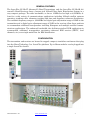
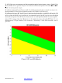
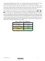
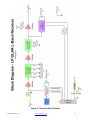
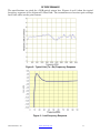
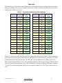
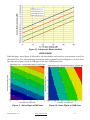
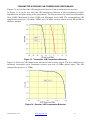
LaserPlus Model LP-OLAT/LP-OLAR
Advanced L-Band Series
10-4,000 MHz
OPERATING MANUAL
24926 Highway 108
Sierra Village, CA 95346
Phone: (800) 545-1022
Fax: (209 586-1022
025-000580 Rev. X1
E-Mail: [email protected]
05/05/11
TABLE OF CONTENTS
Table of Contents .................................................................................................................... 2
Safety ....................................................................................................................................... 3
Safety Precautions.................................................................................................................. 3
Laser Safety Procedure.......................................................................................................... 3
GENERAL FEATURES ............................................................................................................ 4
TRANSMITTER DESCRIPTION............................................................................................... 5
Transmitter Control Overview ...................................................................................... 5
RECEIVER DESCRIPTION ...................................................................................................... 7
Receiver Control Overview ............................................................................................ 7
TRANSMITTER BLOCK DIAGRAM ........................................................................................ 9
RECEIVER BLOCK DIAGRAM.............................................................................................. 10
RF PERFORMANCE .............................................................................................................. 11
LINK GAIN ............................................................................................................................. 12
NOISE FIGURE ...................................................................................................................... 13
TRANSMITTER & RECEIVER 1dB COMPRESSION PERFORMANCE............................... 14
TRANSMITTER & RECEIVER IP2 & IP3 PERFORMANCE .................................................. 15
TRANSMITTER & RECEIVER RF LEVEL DETECTOR PERFORMANCE............................ 16
OPTICAL PERFORMANCE ................................................................................................... 18
CONNECTIONS AND CONTROLS - TRANSMITTER........................................................... 19
CONNECTIONS AND CONTROLS - RECEIVER .................................................................. 19
INSTALLATION...................................................................................................................... 20
Optical Connectors..................................................................................................... 200
Cleaning Optical Connectors ..................................................................................... 200
Mounting .................................................................................................................... 200
ORDERING INFORMATION .................................................................................................. 21
Transmitter Part Numbers ......................................................................................... 21
Receiver Part Numbers................................................................................................ 21
025-000580 Rev. X1
www.olsontech.com
2
SAFETY
Safety Precautions
The optical emissions from the units are laser-based and may present eye hazards if improperly used. NEVER USE ANY KIND OF OPTICAL INSTRUMENT TO VIEW THE OPTICAL OUTPUT OF THE UNIT. Be careful when working with optical fibers. Fibers can
cause painful injury if they penetrate the skin.
Laser Safety Procedures
ALWAYS read the product data sheet and the laser safety label before powering the product.
Note the operation wavelength, optical output power and safety classifications.
If safety goggles or other eye protection are used, be certain that the protection is effective at
the wavelength emitted by the device under test BEFORE applying power.
ALWAYS connect a fiber to the output of the device BEFORE power is applied. Power must
never be applied without an attached fiber. If the device has a connector output, attach a
connector that is connected to a fiber. This will ensure that all light is confined within the fiber waveguide, virtually eliminating all potential hazard.
NEVER look at the end of the fiber to see if light is coming out. NEVER! Most fiber optic laser
wavelengths (1310 nm and 1550 nm) are totally invisible to the unaided eye and will cause
permanent damage. Shorter wavelengths lasers (e.g., 780 nm) may be visible and are very
damaging. Always use instruments, such as an optical power meter, to verify light output.
NEVER, NEVER, NEVER look into the end of a fiber on a powered device with ANY sort of
magnifying device. This includes microscopes, eye loupes and magnifying glasses. This WILL
cause a permanent and irreversible burn on your retina. Always double check that power is
disconnected before using such devices. If possible, completely disconnect the unit from any
power source.
If you have questions about laser safety procedures, please call Olson Technology before
powering your product.
025-000580 Rev. X1
www.olsontech.com
3
GENERAL FEATURES
The LaserPlus LP-OLAT Advanced L-Band Transmitters and the LaserPlus LP-OLAR Advanced L-Band Receivers form a feature-rich L-Band Fiber Optic Distribution System in a
very compact package. The wide bandwidth, as low as 10MHz and as high as 4,000MHz, allows for a wide variety of communications applications including L-Band satellite antenna
remoting, trunking radio, telemetry tracking and time and frequency reference distribution.
The extended frequency range to 4,000MHz and digital gain adjustment range of 25dB in the
transmitter and a digital gain adjustment range of 25dB in the receiver allow these products
to accommodate additional transponders including European and multiple satellite communications applications. The enhanced bandwidth also facilitates stacked LNB applications to
accommodate additional transponders containing enhanced DBS services (HDTV, local
channels, etc.) over single-mode fiber for DBS distribution.
CONFIGURATION
The transmitter and receiver are housed in rugged, compact, standalone enclosures that plug
into the Olson Technology, Inc. LaserPlus platform. Up to fifteen modules can be plugged into
a single LaserPlus chassis.
025-000580 Rev. X1
www.olsontech.com
4
TRANSMITTER DESCRIPTION
The LP-OLAT Transmitter carries 10MHz to 4,000MHz RF signals over single-mode optical
fiber. Model LP-OLAT includes an adjustable 25dB digital gain control. Laser power options
include +4dBm/2.5mW (DFB, CWDM), +5dBm/3mW (DFB) or +10dBm/10mW (DFB, DWDM).
Built-in test points, LED indicators and alarms allow the transmitter to be easily set up and
maintained.
Figure 1 - Annotated Front & Rear View of Transmitter
TRANSMITTER CONTROLS OVERVIEW
On the front of the transmitter, the user can change the gain of the transmitter over a 25dB
range using S1 & S2. Higher gain allows the transmitter to be used with lower level RF signals and vice versa. S1 is a 16-position, hexadecimal, rotary switch. The “0” setting is minimum gain and the “F” setting is the maximum gain. Each position is equal to a 1dB gain
change. So the gain of the “F” setting compared to the gain of the “0” setting will be 15dB
higher. The bottom switch of S2 is a high/low gain setting. When it is in the “Lo” position, the
incremental gain is 0dB. When it is “Hi” position, the gain increases by 10dB. To set the
transmitter for minimum gain, set S1 to “0” and the bottom switch of S2 to the left. To set the
transmitter for maximum gain, set S1 to “F” and the bottom switch of S2 to the right.
025-000580 Rev. X1
www.olsontech.com
5
J1 & J3 allow easy measurement of the transmitter optical output power using a Digital Volt
Meter (DVM). J1 is a ground. J3 gives an indication of the laser power. The scale factor is 0.1
V/mW. J2 is the optical output.
D1 indicates that the Laser Power is OK. It will be green if the laser control circuitry is behaving normally. If the laser or control circuitry fails, then D1 will turn red.
D2 indicates the input RF Level. Figure 2 indicates the thresholds at which D2 will switch. D2
will be yellow if the RF level is below the low threshold, red if the RF level is above the high
threshold and green if the RF level is between the low and high thresholds. For most applications, if D2 is green, then the RF level is in the optimum range. J4 is the RF Input. It is a
high-frequency F-Type Female (75Ω) Connector. Alternately a 50Ω SMA connector can be
provided.
Figure 2 - RF Level (D2) Behavior
025-000580 Rev. X1
www.olsontech.com
6
RECEIVER DESCRIPTION
The OLAR L-Band Receiver can handle 10MHz to 4,000MHz RF signals. The receiver includes
a 25dB digital gain control. Optical input power ranges from -15 to +3dBm in the wavelength
range of 1270-1610nm. The receiver offers high sensitivity for an expanded optical link budget
from -22dBm to -3dBm. Built-in test points, LED indicators and alarms allow the receiver to
be easily set up and maintained.
Figure 3 - Annotated Front & Rear View of Receiver
RECEIVER CONTROLS OVERVIEW
Figure 3 shows the front and rear panels of the receiver.
On the front of the transmitter, the user can change the gain of the transmitter over a 25dB
range using S1 & S2. Higher gain allows the transmitter to be used with lower level RF signals and vice versa. S1 is a 16-position, hexadecimal, rotary switch. The “0” setting is minimum gain and the “F” setting is the maximum gain. Each position is equal to a 1dB gain
change. So the gain of the “F” setting compared to the gain of the “0” setting will be 15dB
higher. The bottom switch of S2 is a high/low gain setting. When it is in the “Lo” position, the
incremental gain is 0dB. When it is “Hi” position, the gain increases by 10dB. To set the
025-000580 Rev. X1
www.olsontech.com
7
transmitter for minimum gain, set S1 to “0” and the bottom switch of S2 to the left. To set the
transmitter for maximum gain, set S1 to “F” and the bottom switch of S2 to the right.
The top switch of S2 also allows the final RF amplifier to be switched on or off (Mute). When
the receiver output is Muted, the RF output level typically drops by 30dB. Note that the RF
Level detector (discussed later) still functions as though the receiver is not muted.
J1 & J3 allow easy measurement of the transmitter optical output power using a Digital Volt
Meter (DVM). J1 is a ground. J3 gives an indication of the Optical Input Power. The scale
factor is 1.0 V/mW. J2 is the optical input. D1 indicates the RF Output Power level. D2 indicates the input RF Level. Figure 2 indicates the thresholds at which D2 will switch. D2 will be
yellow if the RF level is below the low threshold, red if the RF level is above the high threshold
and green if the RF level is between the low and high thresholds. For most applications, if D2
is green, then the RF level is in the optimum range. Table 1 shows the behavior of the Receiver D2 LED. J4 is the RF Output. It is a high-frequency F-Type Female (75Ω) Connector.
Alternately a 50Ω SMA connector can be provided.
Table 1 - Receiver D2 LED Behavior
RF Output Level
D2 LED Color
<-37dBm
Yellow
≥-37dBm and ≤ -22dBm
Green
>-22dBm
Red
Note: This holds true even if the Receiver output is Muted
025-000580 Rev. X1
www.olsontech.com
8
Figure 5 - Transmitter Block Diagram
025-000580 Rev. X1
www.olsontech.com
9
Figure 6 - Receiver Block Diagram
025-000580 Rev. X1
www.olsontech.com
10
RF PERFORMANCE
The specifications are cited for >55dB optical return loss. Figures 8 and 9 show the typical
frequency response of the Advanced L-Band link. The transmitter and receiver gain settings
have little effect on the gain flatness.
Figure 8 - Typical Link (Tx + Rx) Frequency Response
Figure 9 - Low-Frequency Response
025-000580 Rev. X1
www.olsontech.com
11
LINK GAIN
The overall gain of the Advanced L-Band link is affected by the gain setting of the transmitter,
the gain setting of the receiver and the optical loss. Table 2 shows how the gain of the transmitter and receiver can be set.
Table 2 - Transmitter and Receiver Gain Settings
S1
Setting
S2
Setting
Tx or Rx
Gain
S1
Setting
S2
Setting
Tx or Rx
Gain
0
Lo
0dB
0
Hi
10dB
1
Lo
1dB
1
Hi
11dB
2
Lo
2dB
2
Hi
12dB
3
Lo
3dB
3
Hi
13dB
4
Lo
4dB
4
Hi
14dB
5
Lo
5dB
5
Hi
15dB
6
Lo
6dB
6
Hi
16dB
7
Lo
7dB
7
Hi
17dB
8
Lo
8dB
8
Hi
18dB
9
Lo
9dB
9
Hi
19dB
A
Lo
10dB
A
Hi
20dB
B
Lo
11dB
B
Hi
21dB
C
Lo
12dB
C
Hi
22dB
D
Lo
13dB
D
Hi
23dB
E
Lo
14dB
E
Hi
24dB
F
Lo
15dB
F
Hi
25dB
Figure 10 shows how the overall gain of the Advanced L-Band link varies as the transmitter
and receiver gain and optical loss vary. For simplification, the horizontal axis shows the total
of the transmitter and receiver gain. The RF gain changes 2dB for each 1dB of optical loss.
The curves shown in Figure 10 are for a normal sensitivity, PIN-based receiver. The curves in
Figure 10 will all shift upward about 7dB to 20dB when a high-sensitivity APD-based receiver
is used. The variation depends on the receiver optical input level. See Figure 19 for more details.
025-000580 Rev. X1
www.olsontech.com
12
Figure 10 - Advanced L-Band Link Gain
NOISE FIGURE
Like link gain, noise figure is affected by the transmitter and receiver gain settings as well as
the optical loss. The relationship is somewhat more complex however. Figures 11 and 12 show
how the noise figure varies at 3dB optical loss and 15dB optical loss.
Figure 11 - Noise Figure at 3dB Loss
025-000580 Rev. X1
www.olsontech.com
Figure 12 - Noise Figure at 15dB Loss
13
TRANSMITTER & RECEIVER 1dB COMPRESSION PERFORMANCE
Figures 13 and 14 show the 1dB compression behavior of the transmitter and receiver.
In Figure 13, it can be seen that the 1dB compression behavior of the transmitter is highly
dependent on the gain setting of the transmitter. The Figure shows the behavior at Maximum
Gain (25dB), Maximum-10 Gain (15dB) and Minimum Gain (0dB). The corresponding 1dB
compression points are -12.5dBm, -2dBm and +12.5dBm varying almost exactly dB per dB as
the gain changes.
Figure 13 - Transmitter 1dB Compression Behavior
Figure 14 shows the 1dB compression behavior of the receiver output. The test conditions are
minimum transmitter gain, maximum receiver gain and +3.5dBm optical input. The 1dB
compression point is +11.7dBm.
Figure 14 - Receiver 1dB Compression Behavior
025-000580 Rev. X1
www.olsontech.com
14
TRANSMITTER & RECEIVER IP2 & IP3 PERFORMANCE
Figure 15 shows the IP2 and IP3 performance of the transmitter. The test conditions were
with maximum transmitter gain, minimum Rx gain and 0dBm receiver optical input. The
dark blue, dark green and red lines are actual data. The light blue, light green and yellow
lines are extrapolated. Under these conditions, the IP2 is -6.5dBm and the IP3 is -9.5dBm.
Note that these will increase dB per dB as the transmitter gain is lowered.
Figure 15 - Transmitter IP2 & IP3 Behavior
Figure 16 shows the IP2 and IP3 performance of the receiver. The test conditions were with
minimum transmitter gain, maximum Rx gain and +3.5dBm receiver optical input. The dark
blue, dark green and red lines are actual data. The light blue, light green and yellow lines are
extrapolated. Under these conditions, the IP2 is +20dBm and the IP3 is +12dBm. (Note: These
values are read off of the vertical axis.) These will not change significantly as the receiver gain
changes.
Figure 16 - Receiver IP2 & IP3 Behavior
025-000580 Rev. X1
www.olsontech.com
15
TRANSMITTER & RECEIVER RF LEVEL DETECTOR PERFORMANCE
Figures 17 and 18 show behavior of the transmitter and receiver RF Level Detectors.
Figure 17 shows the behavior of the transmitter RF Level Detector at Maximum Gain (25dB),
Maximum-10 Gain (15dB) and Minimum Gain (0dB). To use the chart, first determine the
transmitter gain and measure the voltage out of the RF Level Detector. Then use the chart to
estimate the total RF Level in to the transmitter.
Figure 17 - Transmitter RF Level Detector Behavior
Figure 18 shows the behavior of the receiver RF Level Detector for a normal sensitivity
PIN-based receiver. To use the chart, measure the voltage out of the RF Level Detector, then
use the chart to estimate the total RF Level out of the receiver. Contact the factory for the
response of a high-sensitivity APD-based rteceiver.
Figure 18 - Receiver RF Level Detector Behavior
025-000580 Rev. X1
www.olsontech.com
16
Figure 19 - Gain Advantage - APD vs. PIN Receivers
Figure 20 - SNR Advantage - APD vs. PIN Receivers
025-000580 Rev. X1
www.olsontech.com
17
TABLE 3 - OPTICAL PERFORMANCE
Item
Specification
Optical Fiber
Single Mode 9/125µm (Corning SMF-28 or Equiv.)
Tx/ Rx Optical Return Loss
>55dB
Tx/ Rx Optical Connector
SC/APC (Standard) FC/APC (Optional)
Rx Wavelength
1270-1610nm
Normal Sensitivity PIN-based Rx Optical Input Power
-15 to +3dBm
High Sensitivity APD-based Rx Optical Input Power
-22 to -3dBm
Tx Model #
D4
D5
C4
Tx Laser Type
DFB
DFB
DFB/CWDM
EX
DFB/DWDM
Tx Output Power
+4dBm
+5dBm
+4dBm
+10dBm
Tx Wavelength
1550nm
1310nm
zz
yy
Tx/ Normal Sensitivity Rx
Link Optical Budget
1dB to 19dB
2dB to 20dB
1dB to 20dB
7dB to 25dB
Tx/ High Sensitivity Rx
Link Optical Budget
7dB to 26dB
8dB to 27dB
7dB to 26dB
13dB to 32dB
zz = 47, 49, 51, 53, 57, 59, 61 for each of the available ITU-grid CWDM wavelengths.
yy = 22, 23, …45, 46 for each of the available ITU-grid DWDM wavelengths. (Availability of
some DWDM channels is limited at times.)
025-000580 Rev. X1
www.olsontech.com
18
CONNECTIONS & CONTROLS
TRANSMITTER
Refer to Figure 1 for clarification of terminology
S1
Hexadecimal rotary switch. Changes the gain in 1dB steps from 0 dB to 15dB. The “0”
setting corresponds to 0dB gain. The “F” setting corresponds to 15dB gain. See Table 2 for
more details.
S2
The bottom position switches the gain from HI to LO by switching in 0dB or 10dB attenuation. See Table 2 for more details.
J1
A ground point for a Digital Volt Meter (DVM) probe
J2
Optical Output
J3
Laser Power test point for a DVM probe. Output is 1 Volt/mW
J4
RF Input, 50 Ohms or 75 Ohms (Located on back of the unit.)
D1 Laser Power. Green when laser output is OK. Dark when laser fails.
D2 RF Level. Red if RF level is too high, Yellow if RF level is too low and Green if RF level is
within normal limits.
D3 Laser Temperature (DWDM Laser Models Only). Green indicates good, red bad.
CONNECTIONS & CONTROLS
RECEIVER
Refer to Figure 3 for clarification of terminology
S1
Hexadecimal rotary switch. Changes the gain in 1dB steps from 0 dB to 15dB
S2
The top position is used to MUTE the RF output by removing power form the final amplifier stage. The bottom position switches the gain from HI to LO by switching in 0dB or
10dB attenuation.
J1
A ground point for a Digital Volt Meter (DVM) probe
J2
Optical Input
J3
Optical Input Power test point for a DVM probe. Output is 1 Volt/mW
J4
RF Input, 50 Ohms or 75 Ohms (Located on back of the unit.)
D1 RF Level. Red if RF level is too high, Yellow if RF level is too low and Green if RF level is
within normal limits.
D2 Power indicator. Green when normal.
D3 Optical Input Level. Red if RF level is too high, Yellow if RF level is too low and Green if
level is within normal limits.
025-000580 Rev. X1
www.olsontech.com
19
INSTALLATION
Optical Connectors
There are many optical connectors on the market. There are also different ways the end of the
optical connector is polished, typically “Flat” and “Angle”. The L-Band link is only offered with
SC/APC and FC/APC types of connectors (Angle Polish Connector). One of the most common
errors encountered in the field is the use of the wrong type of connectors. The most common is
using SC/PC or SC/UPC (Flat) with SC/APC (Angled). The connectors will fit together but the
optical loss will be high, performance is totally unpredictable and both connectors may be
permanently damaged.
Cleaning Optical Connectors
Fiber optic connectors should be clean and capped, so one can usually remove the cap and
make the connection without cleaning the connector. If there is any doubt, it is good practice
to clean the optical connectors before making the connection. ALWAYS be certain that the fiber optic connectors have no light before cleaning or inspecting. Once the connection is made,
there should be no need clean the connector as long as the connector remains connected.
Use caution when handling the connectors. Any grease from your finger, scratches or small
pieces of dust or dirt can strongly affect performance. To clean a connector, use a lint-free wipe
such as Kimwipes or cotton swab, moisten with alcohol and gently wipe the tip of the connector. Let the connector air dry completely or use dry compressed air to dry.
When making the connection, be sure the key is aligned with the bulkhead connector. With SC
connectors, gently press in until the connector “clicks” in to place.
Mounting
It is suggested that the modules be mounted with the RF and Optical connectors mounted
down to prevent moisture from entering the connectors. For outdoor or high humidity environments, always use a watertight enclosure.
Connect the optical fiber to both the transmitter and receiver. Insure the optical loss to the
receiver is less than the maximum allowed.
Verify the proper RF level out of the LNB and connect the LNB output to the RF input of the
transmitter. Adjust the transmitter and receiver gain as required.
Connect the RF out of the receiver to the distribution amplifier or TV set top receiver.
Apply power to both modules, the system should now be operational.
025-000580 Rev. X1
www.olsontech.com
20
ORDERING INFORMATION
TRANSMITTER PART NUMBERS
LP-OLAT-X4013-D5-xx-SA
Transmitter, 4GHz, 1310nm, +5dBm/3mW DFB Laser, SC/APC
LP-OLAT-X4013-D5-xx-FA
Transmitter, 4GHz, 1310nm, +5dBm/3mW DFB Laser, FC/APC
LP-OLAT-X4015-D4-xx-SA
Transmitter, 4GHz, 1550nm, +4dBm/2.5mW DFB Laser, SC/APC
LP-OLAT-X4015-D4-xx-FA
Transmitter, 4GHz, 1550nm, +4dBm/2.5mW DFB Laser, FC/APC
LP-OLAT-X40zz-C4-xx-SA
Transmitter, 4GHz, CWDM Wavelengths, +4dBm/2.5mW DFB Laser, SC/APC
LP-OLAT-X40zz-C4-xx-FA
Transmitter, 4GHz, CWDM Wavelengths, +4dBm/2.5mW DFB Laser, FC/APC
LP-OLAT-X40yy-E10-xx-SA
Transmitter, 4GHz, DWDM Wavelengths, +10dBm/10mW DFB Laser, SC/APC
LP-OLAT-X40yy-E10-xx-FA
Transmitter, 4GHz, DWDM Wavelengths, +10dBm/10mW DFB Laser, FC/APC
NOTES:
1) The “zz” in the CWDM number may be 47, 49, 51, 53, 55, 57, 59, 61, for each of the eight available ITU-grid CWDM wavelengths.
2) The “yy” in the DWDM number may be 22, 23, ...45, 46 for each of the available ITU-grid DWDM wavelengths (Note: Availability of some
DWDM channels is limited at times).
3) The “xx” in the part number is the impedance. “xx” = 50 for 50 Ohm, SMA connector. “xx” = 75 for 75 Ohm, F connector.
RECEIVER PART NUMBERS
LP-OLAR-X4000-75-FA
LaserPlus Advanced L-Band Receiver, 4GHz, PIN Detector, 75 Ohm F Connector, FC/APC
LP-OLAR-X4000-75-SA
LaserPlus Advanced L-Band Receiver, 4GHz, PIN Detector, 75 Ohm F Connector, SC/APC
LP-OLAR-X4000-50-FA
LaserPlus Advanced L-Band Receiver, 4GHz, PIN Detector, 50 Ohm SMA Connector, FC/APC
LP-OLAR-X4000-50-SA
LaserPlus Advanced L-Band Receiver, 4GHz, PIN Detector, 50 Ohm SMA Connector, SC/APC
LP-OLAR-X4000S-75-FA
LaserPlus Advanced L-Band Receiver, 4GHz, APD Detector, 75 Ohm F Connector, FC/APC
LP-OLAR-X4000S-75-SA
LaserPlus Advanced L-Band Receiver, 4GHz, APD Detector, 75 Ohm F Connector, SC/APC
LP-OLAR-X4000S-50-FA
LaserPlus Advanced L-Band Receiver, 4GHz, APD Detector, 50 Ohm SMA Connector, FC/APC
LP-OLAR-X4000S-50-SA
LaserPlus Advanced L-Band Receiver, 4GHz, APD Detector, 50 Ohm SMA Connector, SC/APC
025-000580 Rev. X1
www.olsontech.com
21