1
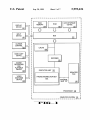
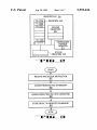
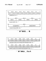
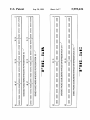
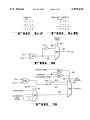
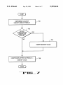
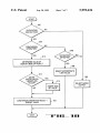
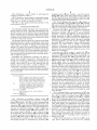
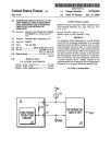
US005959636A
United States Patent [19]
[11]
Patent Number:
Lin et al.
[45]
Date of Patent:
5,959,636
Sep. 28, 1999
[54]
METHOD AND APPARATUS FOR
PERFORMING SATURATION
INSTRUCTIONS USING SATURATION LIMIT
VALUES
Sun Micro., “SPARC Technology Business”, Sep. 1994.
Y. KaWakami, “A Single Chip Digital Signal Processor for
Voiceband Applications”, IEEE, pp. 40&41, Feb. 13, 1980.
J. Shipnes, “Graphics Processing With the 88110 RISC”,
[75]
Inventors: Derrick C. Lin, Foster City; Mehrdad
Mohebbi; Kay K. Huang, both of San
Jose, all of Calif.
Motorola Inc., “MC88110 Second Generation RISC Micro
processor User’s Manual”, 1991.
IEEE, pp. 169—174, 1992.
Motorola Inc. “Errata to MC88110 Second Generation RISC
[73] Assignee: Intel Corporation, Santa Clara, Calif.
[21] Appl. No.: 08/606,328
Microprocessor User’s Manual”, pp. 1—11, 1992.
Motorola Inc., “MCC88110 Programmer’s Reference
Guide”, pp. 1—5, 1992.
[22]
Filed:
Intel, “i860 Microprocessor Family Programmer’s Refer
[51]
Int. Cl.6 .................................................... .. G06F 3/153
Feb. 23, 1996
ence Manual”, Ch. 1,3,8 and 12, 1992.
[52]
US. Cl. ............................................................ .. 345/501
[58]
Field of Search ...................... .. 364/DIG. 1, DIG. 2;
Ruby B. Lee, “Accelerating Mutimedia With Enhanced
Microprocessors”, IEEE Micro, pp. 22—32, Apr. 1995.
Intel, “Pentium Processor User’s Manual, vol. 3: Architec
ture & Programming Manual”, Ch. 1,3,4,6,8 and 18, 1993.
395/118, 126, 128, 129, 130, 131, 132,
133, 376, 501, 523, 526; 345/501, 118
[56]
N. Margulis, “i860 Microprocessor Architecture”, Ch. 6,7,
8,10 and 11, 1990.
References Cited
Primary Examiner—Robert B. Harrell
U.S. PATENT DOCUMENTS
3,711,692
1/1973
3,723,715
3/1973 Chen etal.
364/786
4,161,784
7/1979 Cushing et al. .
364/748
4,393,468
7/1983
364/736
Batcher .............................. .. 364/7158
New ............... ..
4,418,383 11/1983 Doyle et al.
4,498,177
4,707,800
4,771,379
2/1985
Attorney, Agent, or Firm—Blakely, Sokoloff, Taylor &
Larson
Zafman
[57]
395/307
.. ... ... ... ..
. . . . ..
11/1987 Montrone et al.
A method and apparatus for processing saturation instruc
tions in a computer system. A?rst logic device is coupled to
371/52
.. 364/788
9/1988 Ando et al. .... ..
receive at least one carry signal and generate an output
395/800
4,989,168
1/1991 Kuroda et al.
5,095,457
3/1992 Jeong ................. ..
364/758
5,187,679
2/1993 Vassiliadis et al. ..
364/786
5,231,694
7/1993
ABSTRACT
signal in response to the carry signal. A second logic device
is coupled to the ?rst logic device. The second logic device
is capable of selecting between a ?rst plurality of input
signals to generate an output signal. The output signal from
the second logic device represents the result of the saturation
instruction. A third logic device is coupled to the second
logic device. The third logic device is coupled to receive a
second plurality of input signals and generates an output
364/715.09
Novak et al. ......................... .. 395/501
OTHER PUBLICATIONS
B. Case, “Philips Hopes to Displace DSPs With VLIW”,
Microprocessor Report, pp. 12—18, Dec. 05, 1994.
signal. The second plurality of input signals include limit
Texas Instruments, “TMS320C2X User’s Guide”, pp. 3—2
thru 3—34; 4—1 thru 4—151, 1993.
L. GWennnap, “New PA—RISC Processor Decodes MPEG
values corresponding to particular data formats.
Video”, Microprocessor Report, pp. 16—17, Jan. 24, 1994.
15 Claims, 7 Drawing Sheets
SIGN BIT (MSB)
COMPARE i
NOT SIGN BIT (M85)
NOT
COMPARE
860
854 :E 864)
)
SELECT
864
870
ADDER RESULT
see
868
SATURATION
LIMIT
VALUES
OUT
-—
0.
\
U.S. Patent
Sep. 28, 1999
Sheet 2 0f 7
REGISTER FILE @
R0 gg .JREGISTERS 209
R1 2%)
R2 a’
INTEGER
REGISTERS
291
63
R7 M
0
INSTRUCTION
POINTER
REGISTER
g3
STATUS
REGISTERS 208
PII3_2
@
REcEIvE AND DECODE INSTRUCTION
'
w
+
ACCESS REGISTER FILE OR MEMORY
§QZ
Ir
ENABLE EXECUTION UNIT WITH OPERATION
ES
I
STORE RESULT IN REGISTER 'OR MEMORY
30_4
@E
IF'IE___3
5,959,636
U.S. Patent
63
Sep.28, 1999
56 55
BYTE7
43 47
BYTE6
4o 39
BYTE5
Sheet 3 017
32 31
BYTE4
24 23
BYTE3
5,959,636
1615
BYTE 2
s 7
BYTE1
o
BYTEO
PACKED BYTE 401 J
63
4s 47
WORD 3
32 31
WORD 2
1e 15
WORD 1
o
WORD o
PACKED WORD 402 -/
s3
32 31
o
DOUBLEWORD 1
DOUBLEWORD o
PACKED DOUBLEWOHD 403 J
63
56 55
4s 47
4o 39
32 31
24 23
1615
s 7
o
bbbb bbbb bbbb bbbb bbbb bbbb bbbb bbbb bbbb bbbb bbbb bbbb bbbb bbbb bbbb bbbb
UNSIGNED PACKED BYTE lN-REGISTER REPRESENTATION 510 J
s3
s3 55
4347
4039
32 31
2423
1615
37
o
sbbb bbbb sbbb bbbb sbbb bbbb sbbb bbbb sbbb b_bbb sbbb bbbb sbbb bbbb sbbb bbbb
SIGNED PACKED BYTE |N-REC1sTER REPRESENTATION 511 J
PII3__5A
U.S. Patent
Sep.28, 1999
CARRY IN
Sheet 5 of7
>
CARRYOUT
n
5,959,636
CARRYIN
F\F\
0 1 0 1
O 1 1 1
0 1 O 1
1 1 1 1
1 1 O O
1 O 1 0 O
FIE___EA
FII3__EB
SIGNBIT
(M88)
802
812
806
804
5%
cm 3
0OUT
OUT
808
PIE__3
SIGN BIT (M85)
858
COMPARE i
NOT SIGN BIT (MSB)
—
GIN
Cour
NOT
)E__
854
l \DCF864 3
861
SELECT
COMPARE
860
870
ADDER RESULT
OUT
ass
\
SATURATION
LIMIT
VALUES
_-_- @
:
=
PII3_El
U.S. Patent
Sep.28, 1999
Sheet 6 of7
DETERMINE VALUE OF
5,959,636
J 700
SIGN BIT (MSB) OF RESULT
702
DID AN
OVERFLOW OR
UNDERFLOW
OCCUR?
YES
(
INVERT SIGN BIT VALUE
Y
COMPARISON OPERATION RESULT =
f 706
SIGN BIT VALUE
PIE._7
704
U.S. Patent
Sep.28, 1999
Sheet 7 0f 7
5,959,636
NO
SATURATING
INSTRUCTION?
COMPARISON
OPERATION?
SATURATION
DETECTED?
DETERMINE VALUE OF
SIGN BIT (MSB) OF RESULT
YES
90s
,
(
SELECT APPROPRIATE
LIMIT VALUE
912
DID AN
OVERFLOW OR
uNOERFLOw
902
YES
OCCUR?
I (
(914
SELECT AOOER
INvERT SIGN
- OUTPUT
BIT VALUE
COMPARISON OPERATION RESULT =
J 916 ,
SIGN BIT VALUE
4
EVE)
v
—PI|;__ 1n
5,959,636
1
2
METHOD AND APPARATUS FOR
PERFORMING SATURATION
INSTRUCTIONS USING SATURATION LIMIT
VALUES
around” Without saturation. The result generated in this
example may be smaller than either of the tWo values added
together, a clearly erroneous result. In a multimedia
application, if the addition of tWo values results in an
BACKGROUND OF THE INVENTION
over?oW, the result should be clamped to the maximum
value (Which is closer to the actual result than the “Wrap
around” result).
1. Field of the Invention
KnoWn systems for processing instructions utiliZe ?ags to
The present invention relates to computer systems capable
of processing various instructions. More speci?cally, a sys
tem for processing saturating instructions.
2. Background
In typical computer systems, processors are implemented
10
?ags indicating the type of instruction being executed.
Instead of actually clamping the value of the result to a
maximum or minimum, these knoWn systems simply set an
to operate on values represented by a large number of bits
(e.g., 64) using instructions that produce one result. For
example, the execution of an add instruction Will add
together a ?rst 64-bit value and a second 64-bit value and
store the result as a third 64-bit value. HoWever, multimedia
indicate over?oW or under?oW conditions. These ?ags may
include an over?oW ?ag, an under?oW ?ag, a carry ?ag, and
15
over?oW/under?oW ?ag and alloW the result to “Wrap
around.” Therefore, these systems provide an indication of
Whether an over?oW or under?oW occurred, but do not
clamp the result to an appropriate maximum or minimum
value.
applications require the manipulation of large amounts of
data Which may be represented in a small number of bits. For
SUMMARY OF THE INVENTION
example, graphical data typically requires 8 or 16 bits and
The present invention provides a system for processing
saturating instructions capable of clamping the result of the
sound data typically requires 8 or 16 bits. Each of these
multimedia application requires one or more algorithms,
each requiring a number of operations. For example, an
instruction When the result exceeds the range of permitted
algorithm may require an add, compare and shift operation.
values. When an over?oW or under?oW is detected and
25
saturation is enabled, the invention clamps the operation’s
To improve efficiency of multimedia applications (as Well
as other applications having similar characteristics), prior art
processors provide packed data formats. A packed data
particular data format. The circuit arrangement provided by
format is one in Which the bits typically used to represent a
single value are broken into a number of ?xed-siZe data
tions are processed by handling various saturating instruc
result to an appropriate maximum or minimum value for the
the invention increases the overall speed at Which instruc
tions in different manners.
elements, each of Which represents a separate value. For
example, a 64-bit register may be broken into tWo 32-bit
elements, each representing a separate 32-bit value. In
addition, these prior art processors provide instructions for
separately manipulating each element in these packed data
types in parallel. For example, a packed add instruction adds
together corresponding data elements from a ?rst packed
One embodiment of the invention provides a ?rst logic
device coupled to receive at least one carry signal and
generate an output signal in response to the carry signal. A
35
data and a second packed data. Thus, if a multimedia
algorithm requires a loop containing ?ve operations that
must be performed on a large number of data elements, it is
desirable to pack the data and perform these operations in
parallel using packed data instructions.
formats.
When performing operations on various data types, it may
be desirable to provide saturating instructions; i.e., instruc
tions Which clamp the result of the operation When the result
exceeds the range of permitted values. Clamping means
BRIEF DESCRIPTION OF THE DRAWINGS
45
The present invention is illustrated by Way of example in
the folloWing draWings in Which like references indicate
similar elements. The folloWing draWings disclose various
forcing the operation’s result to a maximum or minimum
value When the result over?oWs or under?oWs the range of
values permitted for the data format. In the case of
embodiments of the present invention for purposes of illus
tration only and are not intended to limit the scope of the
invention.
under?oW, saturation clamps the result to the loWest value in
the range and in the case of over?oW, to the highest value.
The alloWable ranges for various data formats are described
beloW. Various types of saturating instructions include
signed saturating addition and subtraction, unsigned satu
rating addition and subtraction, and greater-than comparison
instructions.
Saturation instructions are particularly important in mul
timedia applications to provide accurate representation of
audio signals, video signals, and other data. Clamping an
operation’s result to a maximum or minimum value prevents
“Wrap-around” of the resulting value. “Wrap-around” refers
to the situation Where the over?oW or under?oW generates a
result Which is inaccurate due to a carry into or out of the
most signi?cant bit of the result. Additional details regarding
over?oW and under?oW are provided beloW. For example, if
tWo values are added together and the result exceeds the
maximum value for the data format, the result Will “wrap
second logic device is coupled to the ?rst logic device and
is capable of selecting betWeen a ?rst plurality of input
signals to generate an output signal. The output signal from
the second logic device represents the result of the saturation
instruction. A third logic device is coupled to the second
logic device and receives a second plurality of input signals
and generates an output signal. The second plurality of input
signals include limit values corresponding to particular data
55
FIG. 1 is a block diagram illustrating an exemplary
computer system according to one embodiment of the inven
tion.
FIG. 2 illustrates a register ?le of the processor shoWn in
FIG. 1.
FIG. 3 is a How diagram illustrating the general steps
performed by the processor to manipulate data.
FIG. 4 illustrates various types of packed data.
FIGS. 5A, 5B, and 5C illustrate in-register packed data
representations according to an embodiment of the inven
tion.
FIGS. 6A and 6B illustrate carry operations performed by
65 an adder circuit.
FIG. 7 is a How diagram illustrating the greater-than
comparison operation.
5,959,636
4
3
FIG. 8 illustrates a circuit capable of performing the
Computer system 100 also includes a read only memory
(ROM) 106, and/or other static storage device, coupled to
comparison operation of FIG. 7.
bus 101 for storing static information and instructions for
processor 109. Data storage device 107 is coupled to bus 101
for storing information and instructions.
FIG. 9 illustrates a circuit capable of generating a proper
result based on the operation being performed and the
detection of an over?oW or under?oW condition.
FIG. 1 also illustrates that processor 109 includes an
execution unit 130, a register ?le 150, a cache 160, a decoder
165, and an internal bus 170. Those skilled in the art Will
FIG. 10 is a How diagram illustrating operation of the
circuit shoWn in FIG. 9.
appreciate that processor 109 contains additional circuitry
DETAILED DESCRIPTION
The folloWing detailed description sets forth numerous
speci?c details to provide a thorough understanding of the
invention. HoWever, those skilled in the art Will appreciate
that the invention may be practiced Without these speci?c
details. In other instances, Well knoWn methods, procedures,
components, and circuits have not been described in detail
10
Which is not necessary to understanding the invention.
Execution unit 130 is used for executing instructions
received by processor 109. In addition to recogniZing
instructions typically implemented in general purpose
15
so as not to obscure the invention.
processors, execution unit 130 recogniZes instructions in
packed instruction set 140 for performing operations on
packed data formats. Packed instruction set 140 includes
instructions for supporting various operations including
The present invention is related to a system for processing
saturating instructions capable of clamping the result of the
saturating instructions. An adder circuit is included Within
processor 109 for performing various addition-related
instruction When the result exceeds the range of permitted
operations. The adder circuit is capable of performing
values. When an over?oW or under?oW is detected and
addition, subtraction, and greater-than comparison
saturation is enabled, the invention clamps the operation’s
operations, as discussed in greater detail beloW. Note that
result to an appropriate maximum or minimum value for the
subtraction may be performed by adding the inverse of the
particular data format. The circuit arrangement provided by
the invention increases the overall speed at Which instruc
tions are processed by handling various saturating instruc
number to be subtracted.
25
tions in different manners.
on processor 109 for storing information, including data. An
embodiment of register ?le 150 is described later With
reference to FIG. 2. Execution unit 130 is coupled to cache
160 and decoder 165. Cache 160 is used to cache data and/or
Throughout the speci?cation, references are made to
various types of packed data formats. These packed data
formats are provided to illustrate the invention and an
example of an environment in Which the invention may
operate. Those skilled in the art Will appreciate that the
invention may be used With a variety of different data
formats and is not limited to packed data instructions.
To provide a foundation for understanding the description
of the embodiments of the invention, the folloWing de?ni
Execution unit 130 is coupled to register ?le 150 by
internal bus 170. Register ?le 150 represents a storage area
35
control signals from, for example, main memory 104.
Decoder 165 is used for decoding instructions received by
processor 109 into control signals and/or microcode entry
points. In response to these control signals and/or microcode
entry points, execution unit 130 performs the appropriate
operations. For example, if an add instruction is received,
decoder 165 causes execution unit 130 to perform the
tions are provided.
required addition; if a subtract instruction is received,
decoder 165 causes execution unit 130 to perform the
Bit X through Bit Y:
de?nes a sub?eld of binary number. For example,
bit ?ve through bit Zero of the byte 001110102
required subtraction; etc. Decoder 165 may be implemented
using any number of different mechanisms (e.g., a look-up
table, a hardWare implementation, a PLA, etc.). Thus, While
the execution of the various instructions by the decoder and
execution unit is represented by a series of if/then
(shown in base tWo) represent the sub?eld 1110102
The ‘2’ following a binary number indicates base 2.
Therefore, 10002 equals 810, While F16 equals 1510.
is a register. A register is any device capable of
storing and providing data. Further functionality
45
of a register is described beloW. A register is not
statements. Rather, any mechanism for logically performing
necessarily, included on the same die or in the
same package as the processor.
this if/then processing is considered to be Within the scope
of the invention.
FIG. 1 additionally shoWs a data storage device 107, such
as a magnetic disk or optical disk, and its corresponding disk
drive, can be coupled to computer system 100. Computer
system 100 can also be coupled via bus 101 to a display
SRC1, SRCZ, and DEST:
identify storage areas (e.g., memory addresses,
registers, etc.)
Sourcel-i and Resultl-i:
represent data.
FIG. 1 illustrates an exemplary computer system 100
according to one embodiment of the invention. Computer
system 100 includes a bus 101, or other communications
device 121 for displaying information to a computer user.
55
tion during execution of instructions by processor 109.
Display device 121 can include a frame buffer, specialiZed
graphics rendering devices, a cathode ray tube (CRT), and/or
a ?at panel display. An alphanumeric input device 122,
hardWare and softWare, for communicating information, and
a processor 109 coupled With bus 101 for processing infor
mation. Processor 109 represents a central processing unit of
any type of architecture, including a CISC or RISC type
architecture. Computer system 100 further includes a ran
dom access memory (RAM) or other dynamic storage
device (referred to as main memory 104), coupled to bus 101
for storing information and instructions to be executed by
processor 109. Main memory 104 also may be used for
storing temporary variables or other intermediate informa
statements, it is understood that the execution of an instruc
tion does not require a serial processing of these if/then
including alphanumeric and other keys, is typically coupled
to bus 101 for communicating information and command
selections to processor 109. Another type of user input
device is cursor control 123, such as a mouse, a trackball, a
pen, a touch screen, or cursor direction keys for communi
cating direction information and command selections to
processor 109, and for controlling cursor movement on
65
display device 121.
Another device Which may be coupled to bus 101 is a hard
copy device 124 Which may be used for printing
5,959,636
5
6
instructions, data, or other information on a medium such as
steps folloWed by processor 109 While performing an opera
tion on packed data, performing an operation on unpacked
data, or performing some other operation.
At step 301, the decoder 165 receives a control signal
paper, ?lm, or similar types of media. Additionally, com
puter system 100 can be coupled to a device for sound
recording, and/or playback 125, such as an audio digitizer
coupled to a microphone for recording information. Further,
from either the cache 160 or bus 101. Decoder 165 decodes
the device may include a speaker Which is coupled to a
the control signal to determine the operations to be per
formed. At step 302, Decoder 165 accesses the register ?le
150, or a location in memory. Registers in the register ?le
digital to analog (D/A) converter for playing back the
digitiZed sounds.
150, or memory locations in the memory, are accessed
Also, computer system 100 can be a terminal in a com
puter netWork (e.g., a LAN). Computer system 100 Would
10
then be a computer subsystem of a computer netWork.
Computer system 100 optionally includes video digitiZing
device 126. Video digitiZing device 126 can be used to
capture video images that can be transmitted to others on the
computer netWork.
15
depending on the register address speci?ed in the control
signal. At step 303, eXecution unit 130 is enabled to perform
the operation on the accessed data. At step 304, the result is
stored back into register ?le 150 according to requirements
of the control signal.
FIG. 4 illustrates packed data-types according to one
In one embodiment, the processor 109 additionally sup
ports an instruction set Which is compatible With the X86
embodiment of the invention. Three packed data formats are
instruction set used by existing processors (such as the
doubleWord 403. Packed byte, in one embodiment of the
illustrated; packed byte 401, packed Word 402, and packed
Pentium® processor) manufactured by Intel Corporation of
invention, is siXty-four bits long containing eight data ele
Santa Clara, Calif. Thus, in one embodiment, processor 109
ments. Each data element is one byte long. Generally, a data
element is an individual piece of data that is stored in a
supports all the operations supported in the IATM—Intel
Architecture, as de?ned by Intel Corporation of Santa Clara,
Calif. (see Microprocessors, Intel Data Books volume 1 and
volume 2, 1992 and 1993, available from Intel of Santa
Clara, Calif.). As a result, processor 109 can support existing
X86 operations in addition to the operations of the invention.
While the invention is described as being incorporated into
single register (or memory location) With other data ele
ments of the same length. In one embodiment of the
processor using a neW instruction set.
invention, the number of data elements stored in a register
is siXty-four bits divided by the length in bits of a data
element. Packed Word 402 is siXty-four bits long and con
tains four Word 402 data elements. Each Word 402 data
element contains siXteen bits of information. Packed double
Word 403 is siXty-four bits long and contains tWo double
Word 403 data elements. Each doubleWord 403 data element
contains thirty-tWo bits of information.
FIG. 2 illustrates the register ?le of the processor accord
ing to one embodiment of the invention. The register ?le 150
storage representation according to one embodiment of the
an X86 based instruction set, alternative embodiments could
incorporate the invention into other instruction sets. For
eXample, the invention could be incorporated into a 64-bit
is used for storing information, including control/status
information, integer data, ?oating point data, and packed
FIG. 5a through 5c illustrate the in-register packed data
35
data. In the embodiment shoWn in FIG. 2, the register ?le
150 includes integer registers 201, registers 209, status
registers 208, and instruction pointer register 211. Status
to be eXecuted. Integer registers 201, registers 209, status
registers 208, and instruction pointer register 211 are all
coupled to internal bus 170. Any additional registers Would
ments may be implemented to contain more or less sets of
can noW be performed on eight data elements simulta
45
registers.
neously. Signed packed byte in-register representation 511
illustrates the storage of a signed packed byte 401. Note that
the eighth bit of each byte data element is the sign indicator.
Unsigned packed Word in-register representation 512
The various sets of registers (e.g., the integer registers
201, the registers 209) may be implemented to include
different numbers of registers and/or to different siZe regis
ters. For eXample, in one embodiment, the integer registers
illustrates hoW Word three through Word Zero are stored in
one register of registers 209. Signed packed Word in-register
representation 513 is similar to the unsigned packed Word
in-register representation 512. Note that the siXteenth bit of
each Word data element is the sign indicator. Unsigned
201 are implemented to store thirty-tWo bits, While the
registers 209 are implemented to store eighty bits (all eighty
bits are used for storing ?oating point data, While only
siXty-four are used for packed data). In addition, registers
510 illustrates the storage of an unsigned packed byte 401 in
one of the registers RO 212a through R7 212h. Information
for each byte data element is stored in bit seven through bit
Zero for byte Zero, bit ?fteen through bit eight for byte one,
bit tWenty-three through bit siXteen for byte tWo, and so on.
Thus, all available bits are used in the register. This storage
arrangement increases the storage ef?ciency of the proces
sor. Also, With eight data elements accessed, one operation
registers 208 indicate the status of processor 109. Instruction
pointer register 211 stores the address of the neXt instruction
also be coupled to internal bus 170. Alternative embodi
invention. Unsigned packed byte in-register representation
packed doubleWord in-register representation 514 shoWs
55
hoW registers 209 store tWo doubleWord data elements.
209 contains eight registers, RO 212a through R7 212h. R1
Signed packed doubleWord in-register representation 515 is
212a, R2 212b and R3 212c are eXamples of individual
registers in registers 209. Thirty-tWo bits of a register in
registers 209 can be moved into an integer register in integer
similar to unsigned packed doubleWord in-register represen
tation 514. Note that the necessary sign bit is the thirty
second bit of the doubleWord data element.
registers 201. Similarly, a value in an integer register can be
moved into thirty-tWo bits of a register in registers 209. In
result of an operation to a maXimum or minimum value
As discussed earlier, saturation instructions clamp the
another embodiment, the integer registers 201 each contain
When the result either over?oWs or under?oWs the range of
permissible values. Clamping means setting the result to a
maXimum or minimum value if the operation result eXceeds
64 bits, and 64 bits of data may be moved betWeen the
integer register 201 and the registers 209.
FIG. 3 is a How diagram illustrating the general steps used
by the processor to manipulate data according to one
embodiment of the invention. That is, FIG. 3 illustrates the
65
the range’s maXimum or minimum value. In the case of
under?oW, saturation clamps the result to the loWest value in
the range and in the case of over?oW, to the highest value.
5,959,636
7
8
The allowable ranges for various data formats are shown in
Table 1.
MSB of the result and a one is also carried out of the MSB.
This does not result in an over?oW, because the addition of
a positive number and a negative number cannot produce an
over?oW condition. Thus, a signed over?oW condition can
only occur When a one is carried into the MSB of the result
and a one is not carried out of the MSB.
TABLE 1
Data Format
Unsigned Byte
Signed Byte
Unsigned Word
Signed Word
Unsigned DoubleWord
Signed DoubleWord
Minimum Value
Maximum Value
O
—128
255
127
0
—32768
0
65535
32767
264-1
—263
When adding a negative number to another negative
10
263-1
For example, using the unsigned byte data format, if an
operation’s result is 258 and saturation is enabled, then the
result is clamped to 255 before being stored into the opera
tion’s destination register. Similarly, if an operation’s result
is —32999 and processor 109 uses signed Word data format
With saturation enabled, then the result is clamped to —32768
no carry into the MSB, but a one is carried out of the MSB.
Since both numbers are negative, each number’s MSB is a
15
When performing an unsigned operation With saturation
enabled, the result of the operation must be tested for an
over?oW or under?oW condition. As illustrated in Table 1,
As illustrated above in Table 1, data may be represented
in either signed or unsigned format. Furthermore, the opera
tions performed on signed or unsigned data may be desig
nated as either saturating or non-saturating operations.
saturating enabled or disabled include addition and subtrac
When operating on unsigned numbers, negative results are
not permitted. Therefore, any result having a negative value
is clamped to Zero. Unsigned over?oW can only occur When
25
tion. Additionally, the greater-than comparison operation
tWo unsigned numbers are added together. Since unsigned
numbers do not have a sign bit, the MSB of the unsigned
number is part of the number being represented. An
unsigned over?oW occurs When a one is carried out of the
generates either a true result (all data bits are set to one) or
a false result (all data bits are set to Zero).
A particular instruction itself indicates Whether it is a
saturating instruction or a non-saturating instruction. The
instruction decoder 165 (shoWn in FIG. 1) generates an
instruction indicating Whether the particular instruction is a
saturating instruction. The instruction itself also indicates
the data format on Which the instruction operates; e.g., byte,
one. If the result of the addition operation has a MSB=0,
then an under?oW has occurred.
before being stored into the operation’s destination register.
Examples of operations Which may be performed With
number, the result must be negative. If an under?oW occurs,
the MSB of the result Will indicate a positive number. Using
an analysis similar to that above With respect to a signed
over?oW, a signed under?oW condition occurs When there is
MSB, indicating that the number of bits present is not
sufficient to represent the result.
Similarly, unsigned under?oW can only occur When sub
tracting tWo unsigned numbers. When subtracting tWo
unsigned numbers, there Will alWays be a carry out from the
MSB if the result is valid. Thus, unsigned under?oW occurs
35
When there is no carry from the MSB.
Word, or doubleWord.
Based on the above discussions, the determination of
Whether a signed over?oW or a signed under?oW has
When performing an operation With saturation enabled,
the result of the operation must be tested for an over?oW or
under?oW condition. Signed over?oW can only occur When
occurred may be illustrated by the folloWing equation:
tWo positive numbers are added together. Similarly, signed
under?oW can only occur When a negative number is added
to another negative number. The most signi?cant bit (MSB)
of a signed number represents the sign associated With the
number. Typically, if the MSB=0, then the number is
positive, and if the MSB=1, the number is negative.
When adding tWo positive numbers (MSB=0), the result
45
must be positive. HoWever, if an over?oW occurs, a one is
Where Cm represents the existence of a carry into the MSB,
Com represents the existence of a carry out from the MSB,
and XOR is the Exclusive-OR function. Both the Cm and
Com signals are generated by an adder circuit as a result of
an addition operation. This equation is illustrated by the
folloWing table:
carried into the MSB of the result, indicating a negative
number. In this over?oW situation, the tWo positive numbers
TABLE 2
each had a MSB=0. Therefore, a one is carried into the MSB
of the result, but there is no carry out from the MSB of the
result. This situation is illustrated in FIG. 6A, Where tWo
positive numbers are added together, but the result indicates
a negative number (MSB=1). Since it is impossible to obtain
a negative number as a result of adding tWo positive
numbers, the result shoWn in FIG. 6A is erroneous. Although
a one is carried into the MSB of the result, there is no carry
out from the MSB. Therefore, an over?oW condition has
occurred and the result must be clamped to the maximum
55
Cin
Com
Cin XOR Com
0
O
1
1
O
1
O
1
O
1
1
O
As mentioned above, an over?oW condition requires both
The ?rst roW of Table 2 illustrates the situation Where
there is no carry in and no carry out, thereby generating Zero
as a result. The resulting Zero indicates a valid result; i.e., no
over?oW or under?oW occurred. The second roW of Table 2
illustrates an under?oW situation; i.e., Where there is a carry
a carry into the MSB of the result and the absence of a carry
out from the MSB. A carry into the MSB alone does not
over?oW, the XOR function in the third column generates a
value before storing the result into the operation’s destina
tion register.
necessarily indicate an over?oW condition. FIG. 6B illus
trates a situation Where a positive number is added to a
negative number. In this situation, a one is carried into the
out, but no carry in. In the case of an under?oW or an
65 result of one. The third roW of Table 2 illustrates an over?oW
situation. The fourth roW of Table 2 illustrates a valid result;
i.e., no over?oW or under?oW.
5,959,636
9
10
As mentioned above, another operation which provides
for saturation is the signed greater-than comparison opera
MSB. As illustrated in FIG. 8, the MSB (sign bit) is used as
the select line for multiplexer 800. Thus, upon generation of
the MSB, multiplexer 800 can immediately select the proper
tion (referred to as the comparison operation), illustrated as
follows:
input signal and generate the corresponding output signal.
FIG. 9 illustrates a circuit for selecting a proper output
based on the operation being performed and the detection of
Comparison Operation: A>B
an over?ow or under?ow condition. The circuit illustrated
increases the overall processing speed by increasing the
speed of the comparison operation while decreasing the
speed of the signed and unsigned over?ow and under?ow
This comparison operation is alternatively illustrated in the
following forms:
10
operations. Amultiplexer 850 is coupled to an Exclusive-OR
gate 852 and an inverter 854 as shown in FIG. 8. Multiplexer
A+NOT B20
Note that (—B) may be represented in 2’s complement form
as (NOT B+1). Since the comparison operation can be
15
850 includes three select lines 856, 858 and 860 for selecting
among three inputs 862, 864, and 866. The signal on select
line 856 selects input 862. The signal on select line 858
selects input 864. Finally, the signal on select line 860
selects input 866. The signal on select line 856 is generated
by AND gate 855, and the signal on select line 858 is
represented as A+NOT B20, the sign bit may be used to
generated by AND gate 857.
determine the result of the comparison. If the MSB (the sign
bit) is Zero, indicating a positive result (20), then the
tion being performed, the data type, and whether the instruc
tion saturated. If a signed comparison operation is being
Multiplexer 850 generates an output based on the instruc
comparison is true. If the MSB is one, indicating a negative
result, then the comparison is false. However, the value of
performed (indicated by COMPARE), then one of the inputs
862 or 864 will be selected as the output of multiplexer 850.
In this situation, the function on select line 860, NOT
the MSB is not accurate if an over?ow or under?ow
occurred as a result of the operation (A+NOT B). If an
over?ow or under?ow is detected, then the sign bit is
incorrect and is indicating the opposite value of the proper
COMPARE, will be false, thereby selecting input 862 or
25
value of the sign bit (MSB) will pass through AND gate 855.
Thus, when a comparison operation is being performed, the
appropriate output will be selected from input 862 or 864,
representing the result of the comparison.
If a comparison operation is not being performed, then
result.
Referring to FIG. 7, a ?owchart illustrates the procedure
used to determine the proper result of a greater-than com
parison operation. At step 700, the value of the sign bit
(MSB) of the initial result from the adder circuit is deter
mined. As discussed above, the sign bit is used to determine
the result of the comparison operation. At step 702, a
COMPARE is false and NOT COMPARE is true. In this
situation, select line 860 selects input 866, thereby ignoring
the signals on inputs 862 and 864. The signal on input 866
is generated by a multiplexer 868 in response to a select
signal on line 870 and a plurality of input signals to the
determination is made regarding whether an over?ow or an
under?ow occurred. As discussed above, this determination
is made using the formula Cm XOR Com. If an over?ow or
under?ow occurred, then the procedure branches to step 704
where the value of the sign bit is inverted. Otherwise, the
procedure branches to step 706 where the ?nal result of the
comparison operation is set equal to the value of the sign bit.
The determination of the result of the comparison opera
tion may be illustrated using the following formula:
35
earlier, saturation occurs when an over?ow or under?ow
condition occurs, and may be detected by using the proce
dures and formulas discussed above. If saturation does not
occur, then select line 870 selects the adder result as the
45
output for multiplexer 868. However, if saturation occurs,
then select line 870 selects the proper saturation limit value
depending on the data format used for the instruction being
performed. For example, if an addition operation is being
performed on two signed bytes and an over?ow occurs, then
the saturation limit value of 127 is selected as the output
Signals Cm and Com are generated by an adder circuit (not
shown) as a result of an addition, subtraction, or greater-than
comparison operation. The output of XOR gate 810 is also
coupled to inverter 812 having an output coupled to input
line 806 of multiplexer 800. The sign bit generated as a
result of the (Cl-n XOR Com) calculation is provided to
multiplexer select line 802. Therefore, when the sign bit is
multiplexer. The input signals provided to multiplexer 868
include the initial result from the adder circuit (i.e., the result
from the adder prior to detecting saturation) and the satu
ration limit values for various data formats, as illustrated in
Table 1. The select signal provided on line 870 indicates the
proper input to select based on the instruction being per
formed and whether saturation occurred. As discussed
Comparison=Sign Bit XNOR(C,-,, XOR CUM)
Referring to FIG. 8, a circuit is shown for implementing
the greater-than comparison operation as described above. A
multiplexer 800 includes a select line 802, an output line
804, and a pair of input lines 806 and 808. An Exclusive-OR
gate 810 receives signals Cm and Com and generates an
output a signal coupled to input line 808 of multiplexer 800.
864. When COMPARE is true, the value of the sign bit
(MSB) will pass through AND gate 857 and the inverted
55
from multiplexer 868. The saturation limit values provided
as inputs to multiplexer 868 represent all possible upper and
lower limit values for all data formats utiliZed by the system.
As illustrated in FIG. 9, the comparison operation requires
fewer levels of logic than required by the signed and
unsigned over?ow and under?ow operations. This produces
Zero, the input on line 806 is selected, and when the sign bit
is one, the input on line 808 is selected.
a faster result for the comparison operation which must wait
for the generation of the MSB from the adder circuit.
As discussed above, the comparison operation (A+NOT
Although the signed and unsigned over?ow/under?ow
B) utiliZes the MSB of the result generated by the adder
operations are performed slower as a result of the additional
circuit to determine whether the comparison is true or false.
level of logic, the values necessary to perform these opera
tions are typically generated before the generation of the
MSB from the adder circuit. Since the necessary values for
these operations are generated faster, the operations are
The comparison operation requires the use of an adder
circuit to determine the result. When an adder circuit adds
two numbers, the MSB is the last bit to be generated by the
adder. Therefore, the greatest delay is incurred while waiting
for the MSB of the result. Since the comparison operation
requires the MSB, it is important to maximiZe the speed at
which the comparison circuitry receives and processes the
65
started before the MSB is generated, thereby compensating
for the additional level of logic. Therefore, the overall speed
of the circuit is increased by the arrangement illustrated in
FIG. 9.
5,959,636
11
12
Referring to FIG. 10, a How diagram illustrates the
operation of the circuit shown in FIG. 9. Step 900 deter
mines Whether the instruction being processed is a saturating
the inverted sign bit indicates a ?nal result of the
comparison operation;
otherWise, the sign bit associated With the initial operation
instruction or a non-saturating instruction. If a non
result is a ?nal result of the comparison operation.
4. The method of claim 2 Wherein the step of selecting an
saturating instruction is being processed, then the initial
output of the adder is selected at step 902 Without any
additional processing. If a saturating instruction is being
processed, then step 904 determines Whether a comparison
operation is being executed. If the operation is not a
comparison, then the routine branches to step 906 Where
saturation detection is performed. Saturation detection
appropriate result by detecting Whether a saturation condi
tion occurred comprises steps of:
detecting Whether a saturation condition occurred;
10
(over?ow or under?oW) may be performed using the pro
cedures and circuits discussed above. If a saturation condi
computer system comprising:
tion is detected at step 906 then the appropriate limit value
a ?rst logic device coupled to receive at least one carry
is selected at step 908, and the operation is complete.
Examples of limit values for various data formats are
illustrated in Table 1 above. If the operation result is
15
non-saturating, then step 906 branches to step 902 Where the
output of the adder is selected as the operation result.
If step 904 determines that a comparison operation is
signal, said ?rst logic device generating an output
signal responsive to said carry signal;
a second logic device coupled to said ?rst logic device,
Wherein said second logic device is capable of selecting
betWeen a ?rst plurality of input signals to generate an
executed, then step 910 determines the value of the sign bit
(MSB) of the initial result. The remaining steps 912, 914,
and 916 operate in a manner similar to that described With
respect to FIG. 7.
From the above description and draWings, it Will be
understood by those skilled in the art that the particular
if a saturation condition occurred, then selecting an appro
priate limit value as a result of the instruction executed.
5. An apparatus for processing saturation instructions in a
25
output signal, said output signal representing a result of
said saturation instruction; and
a third logic device coupled to said second logic device,
Wherein said third logic device is coupled to receive a
second plurality of input signals and to generate an
output signal, said second plurality of input signals
embodiments shoWn and described are for purposes of
illustration only and are not intended to limit the scope of the
including limit values corresponding to particular data
invention. Those skilled in the art Will recogniZe that the
invention may be embodied in other speci?c forms Without
departing from its spirit or essential characteristics. Refer
formats.
6. The apparatus of claim 5 Wherein said ?rst logic device
receives a pair of carry signals generated by an adder.
7. The apparatus of claim 5 Wherein said ?rst logic device
ences to details of particular embodiments are not intended
is an Exclusive-OR gate.
to limit the scope of the claims.
What is claimed is:
1. In a computer system, a method for processing instruc
tions comprising steps of:
receiving an instruction;
8. The apparatus of claim 5 Wherein said carry signal
identi?es carry bits generated during an addition operation.
9. The apparatus of claim 5 Wherein said carry signal
35
addition operation.
determining that said instruction is either a saturating
10. The apparatus of claim 5 Wherein said second logic
instruction or a non-saturating instruction;
if said instruction is a saturating instruction, then gener
device is a multiplexer.
11. The apparatus of claim 5 Wherein said second logic
device selects betWeen said ?rst plurality of input signals
ating a result by determining a type of operation being
based on a sign bit generated by an adder.
executed and detecting Whether a saturation condition
occurred, Wherein the result generated is a limit value
associated With a particular data format;
otherWise, generating a result by selecting an actual
output of the instruction being executed.
2. The method of claim 1 Wherein said step of generating
a result by determining a type of operation being executed
12. The apparatus of claim 5 Wherein said second logic
device selects betWeen said ?rst plurality of input signals in
response to a sign bit generated by an adder and a signal
45
and detecting Whether a saturation condition occurred com
14. The apparatus of claim 5 Wherein said third logic
device is a multiplexer.
executed;
15. An apparatus for processing an instruction in a com
puter system comprising:
if a comparison operation is being executed, then deter
Whether a saturation condition occurred.
3. The method of claim 2 Wherein the step of determining
Whether a saturation condition occurred comprises steps of:
determining a value of a sign bit associated With an initial
operation result;
determining Whether a saturation condition occurred;
if a saturation condition occurred, then inverting the sign
bit associated With the initial operation result, Wherein
13. The apparatus of claim 5 Wherein said third logic
performed and a saturation condition.
determining Whether a comparison operation Was
otherWise, selecting an appropriate result by detecting
indicating a type of operation being performed.
device selects betWeen said second plurality of input signals
in response to signals indicating a type of operation being
prises steps of:
mining Whether a saturation condition occurred and
generating said result in response to a sign bit contained
in an initial operation result;
indicates Whether a saturation condition occurred during an
means for receiving carry signals generated by an adder;
55
means for determining Whether said instruction is either a
saturating instruction or a non-saturating instruction;
means for generating a result based on an instruction type
and a saturation condition if said instruction is a
saturating instruction, Wherein the result is a limit value
associated With a particular data format; and
means for generating a result based on an actual output of
the instruction if said instruction is a non-saturating
instruction.