1
US 20140170971A1
(19)
United States
(12) Patent Application Publication (10) Pub. N0.: US 2014/0170971 A1
WALSH et al.
(54)
(43) Pub. Date:
SYSTEM AND METHOD FOR PROVIDING
(52)
INFORMATION TO AND/OR OBTAINING
Jun. 19, 2014
US. Cl.
CPC ........ .. H04B 5/0031 (2013.01); G06K 7/10544
INFORMATION FROM A COMPONENT OF
(2013.01)
AN ELECTRICAL DISTRIBUTION SYSTEM
USPC .................... .. 455/41.1; 235/454; 235/462.11
(71) Applicant: g?T8§)CORPORATION, Cleveland,
(72)
(57)
Inventors, PATRICK T WALSH Coraopolis PA
Anelectrical distribution system Wherein information is com
' (Us), Deborglh K MO’RT Coraop’ohs
PA (138) D avi d
(US)
municated to and/or from an electrical component of the
ROHN’ Venetia PA
’
l
’
ABSTRACT
electrical distribution system using near-?eld communica
’
tions. The information may be communicated to and/or from
the electrical component using an electronic device such as a
(73) Assignee; EATON CORPORATION, Cleveland,
OH (US)
dedicated near-?eld device, a smartphone or a con?guration
card device. Also, a method of obtaining information from an
(21)
(22)
electrical component of an electrical distribution system,
such as a circuit interrupter, includes generating a machine
readable element that comprises ?rst information in encoded
APPI- NOJ 13/719,477
Filed_
Dec 19 2012
'
'
’
form, the ?rst information relating to the operation and/or
Publication Classi?cation
51
Int. Cl.
H04B 5/00
(2006.01)
G06K 7/10
(2006.01)
status of the circuit interrupter, displaying the machine read
able element on the circuit interrupter, capturing an image of
the machine readable element, obtaining the ?rst information
based on the image, and displaying second information based
on the obtained ?rst information.
L_...1
L..._\
(’5‘. i @ 1f“ \ (a) f‘\
\\M/' O \.j) Q \\..j
2“
\
[3/ 6
a
if? 6
'
CGMMUMCAIEGNS
HANBHELD NFC
DEVECE
v) ,\ \x \\
\z \\
/
\,\
,
v\‘\
/
M
,‘
) ,1 /
14\
\Y
12*.
f
'r
{’
.
.;.........M
LONG
-
SHGRT
.\
more? \.
20"5 567
CHI/1 to 7% C20 49 ‘ {1-8
1\L8/;
A RH 4"
(f/
“\
I
r
l
\W/
,m
1
'5
X
r“?
M“\
1T}
\../
"\I
\
)
_
X
rmv
5
"
129 if
\
‘24 3;, MC'HJ
.M
V]
f
T"\\
\J
A
)4
Patent Application Publication
Jun. 19, 2014 Sheet 1 0f 11
US 2014/0170971 A1
N
6E.
Patent Application Publication
8\
Jun. 19, 2014 Sheet 2 0f 11
SiNSED
\
SiATiiS
CURRENT
US 2014/0170971 A1
TRiP
3EGNAL
A
k
Yum-"mi:
‘* ADC ““““““““““““
TRANSCEEVER
Q;mmmmm
@
g
29‘
AG
CHEF
123
w J48
__________"53m;
>
RX/iX
AQJUSTABLE
swmaas
W
............... ..
25/
13m
;
A
B; EEPRQM
T
V {_
I
Rm
v /,22
24
H615
i6
I
..........._
953%
I
I
|
I
I
1
ma !
,32
j
WU?
APPARATUS
,44
M)
MEMGRY
,42
f
i "" n
TRANNSFCQEWER
m“?
i
i
I
l
!
i
i
WM
1
l
L mmmmmmmmmmmmmmmmmmmmmmmmm mm}
Patent Application Publication
1
Jun. 19, 2014 Sheet 3 0f 11
C,
5%
w
US 2014/0170971 A1
Patent Application Publication
US 2014/0170971 A1
Jun. 19, 2014 Sheet 4 0f 11
45
f
I“ mmmmmmmmmmmmmmmmmmmmmmmmm “MI
I
II
$6 I
K54
i
I
i
IIIEIIIGRY
II‘
a
f
.53
a?
.
I
@I’ II
NR;
i
TRANSCEIVER
i
CHIP
.
\.
I
58
I
I
I
|
PGWER ?g
I
i
i
SUPPLY
i
L mmmmmmmmmmmmmmmmmmmmmmmmm “mi
Patent Application Publication
g/
Jun. 19, 2014 Sheet 5 0f 11
US 2014/0170971 A1
Patent Application Publication
Jun. 19, 2014 Sheet 6 0f 11
54%
I“ mmmmmmmmmmmmm “MW
l
I
II
5%
i
we
TRARSCEWER
CHEF
{58
§
l
I
E I1
L _____________ ____!
US 2014/0170971 A1
Patent Application Publication
Jun. 19, 2014 Sheet 7 0f 11
US 2014/0170971 A1
K.)
®,
Of“\N
in"?
FIGQ
Patent Application Publication
Jun. 19, 2014 Sheet 8 0f 11
US 2014/0170971 A1
FIG .2 0
{£6
52\
/
\i
i!
fm
mm}?
|
APPARATUS
i
!
i%
mm J34
i
(w
W'
i!
gg~f
92
MEMQRYmums fg‘i
f
l
mam
CAMERA
|
\
i
88
i
l
L_ mmmmmmmmmmmmmmmmmmmmmmmmm mm}
FIG.”
Patent Application Publication
Jun. 19, 2014 Sheet 9 0f 11
US 2014/0170971 A1
75
/
ffmmmmmmmm“\
OL ....... ..)
mil
m
Q9
BREAKER TQPPEG
?
CAUSE : SHQRT DELAYNMX
ff...
CUCK FQR -
WAVEFGRMg
@w
\Mmmmmmmmmm/
’”________“\
CG
mi!
9
CQNHGURAHQN
iNFGRMAUON
WCKUP : 5x
?ME I
CUQK FGR CUCK FOR
$353
SERWCE
MANUAL
E?FOQ
FYG2 3
Patent Application Publication
Jun. 19, 2014 Sheet 10 0f 11
(@Mw
US 2014/0170971 A1
FIGOM
0 ($3
A;
Q
U
PHASE VQLTAGES "Wm
W Z5
Patent Application Publication
Jun. 19, 2014 Sheet 11 0f 11
US 2014/0170971 A1
X;
,1
mz5mi
§:2%A
5Q 2 528 A
w FiQJsA
’13-»
.
75
,;__\ f)
01:11:)
W
W M/"HZB
MZMZA
53 I 2% A
5Q = M8 A
@MZ
‘ FYGM‘E
US 2014/0170971Al
SYSTEM AND METHOD FOR PROVIDING
INFORMATION TO AND/OR OBTAINING
INFORMATION FROM A COMPONENT OF
AN ELECTRICAL DISTRIBUTION SYSTEM
BACKGROUND
[0001]
[0002]
1. Field
This invention pertains generally to electrical distri
bution systems that include components such as, without
limitation, circuit interrupters and, more particularly, to sys
tems and methods for providing information, such as, without
limitation, con?guration information, to components (such as
a circuit breaker) of an electrical distribution system and/or
for obtaining information, such as, without limitation, con
?guration information and/or diagnostic information, from
components (such as a circuit breaker) of an electrical distri
bution system.
[0003] 2. Background Information
[0004] Electrical switching apparatus for electrical distri
bution systems, such as circuit interrupters and, in particular,
circuit breakers of the molded case variety, are well known in
the art. See, for example, US. Pat. No. 5,341,191.
[0005] Circuit breakers are used to protect electrical cir
cuitry from damage due to an overcurrent condition, such as
an overload condition or a relatively high level short circuit or
fault condition. Molded case circuit breakers typically
Jun. 19, 2014
device can be established. Typically, the pick-up currents for
the various protection functions have been selectable mul
tiples or fractions of this current rating. Thus, instantaneous
protection trips the device any time the current reaches a
selected multiple of the rated current, such as, for example,
ten times the rated current. Pick-up for short delay protection
is a multiple of the rated current, while pick-up current for
long delay protection may be a fraction of the rated current.
Typically, the short delay trip is only generated when the short
delay pick-up current is exceeded for a short delay time
interval, although, in some applications, an inverse time func
tion is also used for short delay protection.
[0009] Currently, many electronic trip units use adjustable
(e.g., without limitation, rotary) switches to vary functional
trip settings, such as, for example and without limitation, long
delay pickup (Ir), long delay time (LDT), short delay pickup
(SDPU), ground fault pickup (GFPU), and short delay time
and ground fault time (SDT/GFT). The adjustable switches
are typically labeled on a per unit basis and are common to all
current sensor (e. g., current transformer) types.
[0010] There is room for improvement in electrical distri
bution systems that include components such as, without
limitation, circuit interrupters, and, in particular, in the area of
providing information to and/ or obtaining information from
components of an electrical distribution system such as a
circuit breaker.
include separable contacts which may be operated either
manually by way of a handle disposed on the outside of the
case or automatically in response to an overcurrent condition.
Typically, such circuit breakers include: (i) an operating
mechanism which is designed to rapidly open and close the
separable contacts, and (ii) a trip unit which senses overcur
rent conditions in an automatic mode of operation. Upon
sensing an overcurrent condition, the trip unit trips the oper
ating mechanism to a trip state, which moves the separable
contacts to their open position.
[0006]
Industrial circuit breakers often use a circuit breaker
SUMMARY
[0011] In one embodiment, an electrical distribution sys
tem is provided that includes an electrical component having
a ?rst near-?eld communications chip coupled to a ?rst near
?eld communications coupling element, and an electronic
device having a second near-?eld communications chip
coupled to a second near-?eld communications coupling ele
ment, wherein the electronic device is structured to transmit
?rst information to the ?rst near-?eld communications chip
and/or receive second information from the ?rst near-?eld
frame which houses a trip unit. See, for example, US. Pat.
communications chip over a near-?eld communications inter
Nos. 5,910,760; and 6,144,271 . The trip unit may be modular
face established between the ?rst near-?eld communications
coupling element and the second near-?eld communications
and may be replaced in order to alter the electrical properties
of the circuit breaker.
[0007] It is well known to employ trip units which utilize a
microprocessor to detect various types of overcurrent trip
conditions and to provide various protection functions, such
as, for example, a long delay trip, a short delay trip, an
coupling element.
[0012]
In another embodiment, a method of transferring
instantaneous trip, and/or a ground fault trip. The long delay
trip function protects the load served by the protected elec
information in an electrical distribution system having an
electrical component having a ?rst near-?eld communica
tions chip coupled to a ?rst near-?eld communications cou
pling element and an electronic device having a second near
?eld communications chip coupled to a second near-?eld
trical system from overloads and/ or overcurrents. The short
communications coupling element is provided. The method
delay trip function can be used to coordinate tripping of
downstream circuit breakers in a hierarchy of circuit breakers.
The instantaneous trip function protects the electrical con
includes establishing a near-?eld communications interface
between the ?rst near-?eld communications coupling ele
ment and the second near-?eld communications coupling
element, and performing at least one of: (i) transmitting ?rst
ductors to which the circuit breaker is connected from dam
aging overcurrent conditions, such as short circuits. As
information to the ?rst near-?eld communications chip over
implied, the ground fault trip function protects the electrical
the near-?eld communications interface, and (ii) receiving
system from faults to ground.
[0008] Each circuit breaker is designed for a speci?c maxi
second information from the ?rst near-?eld communications
chip over the near-?eld communications interface.
mum continuous current. This current rating may be set by a
[0013]
suitable selection mechanism, such as by a rotary switch or by
selection of a resistor (e. g., a “rating plug”) which converts a
current to a voltage for use by the trip unit. In some instances,
an electrical component having a ?rst near-?eld communica
tions chip coupled to a ?rst near-?eld communications cou
In yet another embodiment, a method of con?guring
a single circuit breaker frame may be easily adapted for
pling element includes providing a con?guration card device
(64) having a second near-?eld communications chip coupled
installations which call for a range of maximum continuous
to a second near-?eld communications coupling element, the
currents, up to the design limits of the frame, through use of
the selection mechanism by which the current rating of the
con?guration card device storing con?guration information
for the electrical component, establishing a near-?eld com
US 2014/0170971A1
munications interface between the ?rst near-?eld communi
cations coupling element and the second near-?eld commu
Jun. 19, 2014
nications coupling element, transmitting the con?guration
[0024] FIG. 8 is a schematic diagram showing certain
selected components of a con?guration card device forming
part of the system of FIG. 6 according to another exemplary
information from the con?guration card device to the ?rst
embodiment;
near-?eld communications chip over the near-?eld commu
[0025]
nications interface, and con?guring the electrical component
system according to another alternative exemplary embodi
ment of the present invention;
based on the con?guration information.
[0014] In still another embodiment, a circuit interrupter
system is provided that includes a circuit interrupter, the
circuit interrupter having a ?rst processor apparatus and a ?rst
display, the ?rst processor apparatus being structured to: (i)
generate a machine readable element that comprises ?rst
information in encoded form, the ?rst information relating to
the operation and/or status of the circuit interrupter, and (ii)
cause the machine readable element to be displayed on the
?rst display, and a portable computing device having a second
processor apparatus, a second display, and an image capture
device, the second processor apparatus being structured to: (i)
FIG. 9 is a schematic diagram of a circuit interrupter
[0026] FIG. 10 is a schematic diagram showing a two
dimensional (2D) barcode display on a display device of a
circuit interrupter of the system of FIG. 9 according to an
exemplary embodiment;
[0027]
FIG. 11 is a schematic diagram ofa portable com
puting device forming part of the system of FIG. 9 according
to an exemplary embodiment; and
[0028] FIGS. 12-16B are top plan views of the portable
computing device of FIGS. 10 and 11 showing a number of
different screens thereof according to various exemplary
embodiments.
cause the image capture device to capture an image of the
DESCRIPTION OF THE PREFERRED
EMBODIMENTS
machine readable element, (ii) obtain the ?rst information
based on the image, and (iii) cause second information to be
displayed on the second display based on the obtained ?rst
information.
[0015]
In yet another embodiment, a method of obtaining
information from an electrical component of an electrical
distribution system, such as a circuit interrupter, includes
generating a machine readable element that comprises ?rst
information in encoded form, the ?rst information relating to
the operation and/or status of the circuit interrupter, display
ing the machine readable element on the circuit interrupter,
capturing an image of the machine readable element, obtain
ing the ?rst information based on the image, and displaying
second information based on the obtained ?rst information.
BRIEF DESCRIPTION OF THE DRAWINGS
[0016]
[0029]
Directional phrases used herein, such as, for
example, left, right, front, back, top, bottom and derivatives
thereof, relate to the orientation of the elements shown in the
drawings and are not limiting upon the claims unless
expressly recited therein.
[0030] As employed herein, the statement that two or more
parts are “coupled” together shall mean that the parts are
joined together either directly or joined through one or more
intermediate parts.
[0031] As employed herein, the term “number” shall mean
one or an integer greater than one (i.e., a plurality).
[0032]
As used herein, “near-?eld communications” or
“NFC” shall mean a technique wherein two devices are
coupled to one another and wirelessly transfer power and/or
A full understanding of the disclosed concept can be
information within the near-?eld over a short distance (such
gained from the following description of the preferred
as, without limitation, about four cm) using coupled inductive
embodiments when read in conjunction with the accompany
circuits. Near-?eld communications are governed by various
standards, such as, without limitation, ISO/IEC 18092,
ECMA-340, ISO/IEC 21481, and ECMA-352.
ing drawings in which:
[0017] FIG. 1 is a schematic diagram of a circuit interrupter
system according to an exemplary embodiment of the present
invention;
[0018] FIG. 2 is a schematic diagram showing certain
selected components of an electronic trip unit forming part of
[0033]
As used herein, the term “near-?eld” shall mean a
region that is in proximity to an electromagnetic radiating
structure, such as an antenna or coil, where the electric and
a circuit interrupter of the system of FIG. 2 according to an
magnetic ?elds do not have a plane-wave characteristic, but
instead vary greatly from one point to another. Furthermore,
exemplary embodiment;
the near-?eld can be subdivided into two regions which are
[0019]
commonly known as the reactive near-?eld and the radiating
near-?eld. The reactive near-?eld is closest to the radiating
structure and contains almost all of the stored energy, whereas
the radiating near-?eld is where the radiation ?eld is domi
FIG. 3 is a schematic diagram showing certain
selected components of an NFC communications device
forming part of the system of FIG. 2 according to an exem
plary embodiment;
[0020] FIG. 4 is a schematic diagram of a circuit interrupter
system according to an alternative exemplary embodiment of
the present invention;
nant over the reactive ?eld but does not possess plane-wave
characteristics and is complicated in structure. This is in
contrast to the far-?eld, which is generally de?ned as the
[0021] FIG. 5 is a schematic diagram showing certain
selected components of an NFC metering module forming
part of the system of FIG. 4 according to an exemplary
acteristic, i.e., it has a uniform distribution of the electric and
magnetic ?eld strength in planes transverse to the direction of
embodiment;
propagation.
[0022]
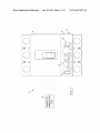
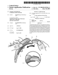
[0034] FIG. 1 is a schematic diagram of a circuit interrupter
system 2 according to an exemplary embodiment of the
present invention. Circuit interrupter system 2 includes a
FIG. 6 is a schematic diagram of a circuit interrupter
system according to another alternative exemplary embodi
ment of the present invention;
[0023] FIG. 7 is a schematic diagram showing certain
selected components of a con?guration card device forming
part of the system of FIG. 6 according to an exemplary
embodiment;
region where the electromagnetic ?eldhas a plane-wave char
con?gurable circuit interrupter 4 (in the illustrated, non-lim
iting embodiment, con?gurable circuit interrupter 4 is a
molded case circuit breaker) having an operating mechanism
6 con?gured to rapidly open and close the separable contacts
US 2014/0170971A1
Jun. 19, 2014
of circuit interrupter 4 and an electronic trip unit 8 operatively
coupled to operating mechanism 6 which, in an automatic
a communication interface 26, which in turn is operatively
coupled to microprocessor 18 to allow for serial communica
mode of operation, is structured to sense overcurrent condi
tions and in response thereto move operating mechanism 6 to
a state wherein the separable contacts of circuit interrupter 4
are open. As seen in FIG. 1, in the illustrated embodiment,
tion with microprocessor 18.
electronic trip unit 8 includes a number of adjustable switches
10 for varying the functional trip settings (such as, for
example and without limitation, long delay pickup (Ir), long
delay time (LDT), short delay pickup (SDPU), ground fault
pickup (GFPU), and short delay time and ground fault time
(SDT/GFT)) of electronic trip unit 8. Electronic trip unit 8
also includes a Serial Port Interface (SPI) 12 and a trip unit
status indicator 14 (in the form of an LED).
[0035]
In addition, circuit interrupter system 2 includes a
handheldNFC communications device 16 that is structured to
communicate with electronic trip unit 8 using near-?eld com
munications (NFC) as described in more detail herein. In this
con?guration, an operator is thus able to: (i) establish func
tional trip settings for electronic trip unit 8 by inputting the
desired settings into a user interface provided on NFC com
munications device 16 (as an alternative to or replacement of
manual switches) and transmitting the settings to electronic
trip unit 8 over an NFC interface established between NFC
communications device 16 and electronic trip unit 8 as
described in greater detail elsewhere herein, and (ii) read the
current functional trip settings for electronic trip unit 8 and/or
other information from electronic trip unit 8 (e.g., stored
information relating to the operation and/ or status of circuit
interrupter 4, such as cause of trip, load, voltage and harmon
ics information described elsewhere herein) using NFC com
munications device 16 and the NFC interface between NFC
communications device 16 and electronic trip unit 8 as
described in greater detail elsewhere herein.
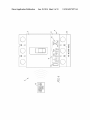
[0036] FIG. 2 is a schematic diagram showing certain
selected components of electronic trip unit 8 according to the
exemplary embodiment. As seen in FIG. 2, electronic trip unit
8 includes a microprocessor (uP) 18 which controls the opera
tion of electronic trip unit 8. Alternatively, microprocessor 18
may be another type of processing or control unit, such as,
without limitation, a microcontroller or some other suitable
processing device. Electronic trip unit 8 further includes an
analog-to-digital converter (ADC) 20, a random access
memory (RAM) 22 and an EEPROM 24, each of which is
coupled to microprocessor 18. ADC 18 is structured to
receive signals, such as a number of current signals (indicat
ing the current of each phase of the system to which circuit
interrupter 4 is connected), that are sensed by sensors (not
shown; e.g., a number of current transformers or Rogowski
coils) forming part of circuit interrupter 4 and convert those
signals to digital data that is appropriate for microprocessor
18.As will be appreciated, that data may be stored in RAM 22
and/ or used by the trip unit program implemented in micro
processor 18 in determining whether and when to issue a trip
signal for tripping operating mechanism 6. In addition, in the
exemplary embodiment, EEPROM 24 stores (in nonvolatile
memory) the functional trip settings (such as, for example and
without limitation, long delay pickup (Ir), long delay time
(LDT), short delay pickup (SDPU), ground fault pickup
[0037]
Electronic trip unit 8 further includes an NFC trans
ceiver chip 28 coupled to an NFC coupling element 30, such
as an antenna or coil. NFC transceiver chip 28 is an integrated
circuit chip that is con?gured to conduct near-?eld commu
nications as described elsewhere herein. In the exemplary
embodiment, NFC transceiver chip 28 includes a wireless
controller portion and a non-volatile memory portion (e.g.,
without limitation, FRAM), and may be, for example and
without limitation, the TRF7970a transceiver chip sold by
Texas Instruments Incorporated or the WM710xx transceiver
chip sold by Ramtron International Corporation. As
described elsewhere herein, NFC transceiver chip 28 coupled
to NFC coupling element 30 allows electronic trip unit 8 to
engage in near-?eld communications with NFC communica
tions device 16.
[0038] FIG. 3 is a schematic diagram showing certain
selected components of NFC communications device 16
according to the exemplary embodiment. NFC communica
tions device 16 may be a device dedicated to the function of
engaging in near-?eld communications with electronic trip
unit 8 as described herein, or, alternatively, may be an elec
tronic device, such as smartphone, having more general pur
pose capabilities (e.g., phone or Internet browsing function
ality) that also has near-?eld communications capabilities
that are speci?cally adapted (e.g., through software) for
engaging in near-?eld communications with electronic trip
unit 8 as described herein.
[0039] As seen in FIG. 3, NFC communications device 16
includes an input apparatus 32 (e.g., without limitation, a
keyboard, a keypad, or a touch screen), a display 34 (e.g.,
without limitation, an LCD), a processor apparatus 36, and a
power supply 38 (e.g., without limitation, a rechargeable
battery). A user is able to provide input into processor appa
ratus 36 using input apparatus 32, and processor apparatus 36
provides output signals to display 34 to enable display 34 to
display information to the user. NFC communications device
16 further includes an NFC transceiver chip 40 (similar to
NFC transceiver chip 28 described herein) coupled to an NFC
coupling element 42 (similar to NFC coupling element 30
described herein). NFC transceiver chip 40 coupled to NFC
coupling element 42 is structured to enable NFC communi
cations device 16 to engage in near-?eld communications
with electronic trip unit 8 through coupling/interaction with
NFC transceiver chip 28 and NFC coupling element 30 as
described in more detail elsewhere herein.
[0040] Processor apparatus 36 comprises a microprocessor
(uP) 44 (or other suitable processing device) and a memory 46
that interfaces with microprocessor 44. Memory 46 can be
any one or more of a variety of types of internal and/or
external storage media such as, without limitation, RAM,
ROM, EPROM(s), EEPROM(s), FLASH, and the like that
provide a storage register, i.e., a machine readable medium,
for data storage such as in the fashion of an internal storage
area of a computer, and can be volatile memory or nonvolatile
memory. Memory 46 has a number of routines stored therein
that are executable by microprocessor 44. One or more of the
(GFPU), and short delay time and ground fault time (SDT/
GFT)) of electronic trip unit 8, which are read into micropro
routines implement (by way of computer/processor execut
cessor 18 as needed by the trip unit program. Electronic trip
unit 8 also includes a serial port interface (SPI) 12 coupled to
able instructions) a software application/system that is con
?gured to, among other things, enable a user to set, monitor,
US 2014/0170971Al
Jun. 19, 2014
display and/or change conditions, parameters, settings and/or
formed when auxiliary power is not being provided to circuit
events within circuit interrupter 4 using near-?eld communi
interrupter 4. In such as case, NFC transceiver chip 28 of
electronic trip unit 8 is con?gured as a passive device. In such
a con?guration, NFC transceiver chip 28 derives the power it
cations as described herein.
[0041]
In operation, NFC communications device 16 may
be used to con?gure circuit interrupter 4 by establishing func
tional trip settings for electronic trip unit 8 in the following
manner (a so-called “programming procedure”). First, using
input apparatus 42, a user inputs the desired settings into NFC
communications device 16. Those settings are stored in
memory 46. The user then brings NFC communications
device 16 into close proximity with electronic trip unit 8. In
particular, NFC communications device 16 is brought close
enough to allow for a near-?eld coupling interface to be
established between NFC communications device 16 and
electronic trip unit 8 (e. g., within 4 cm or less). The user then
initiates a programming procedure using input apparatus 42
(e. g., by pressing a predetermined button). In response, NFC
communications device 16 will cause information including
the stored functional trip settings to be transferred to elec
tronic trip unit 8 over an NFC interface between the two
devices. In particular, NFC transceiver chip 40 will cause
NFC coupling element 42 to radiate an RF near-?eld in a
manner wherein the information to be transferred (the func
needs for operation from the ?eld that is radiated by NFC
coupling element 42 and induced in NFC coupling element
30. As will be appreciated, this capability may be particularly
advantageous in a situation wherein a number of circuit inter
rupters 4 need to be commissioned in an environment, such as
in a new building, where power is not available to the envi
ronment (e. g., the new building has not yet been energized).
Since each of the circuit interrupters 4 can be fully con?gured
with trip settings as just described without the need for aux
iliary power, the environment can be fully commissioned (for
example at the time of initial installation) and ready for opera
tion when the power does becomes available.
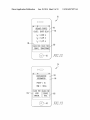
[0045] FIG. 4 is a schematic diagram of a circuit interrupter
system 2' according to an alternative exemplary embodiment
of the present invention. Circuit interrupter system 2' includes
many of the same components as circuit interrupter system 2,
and like components are labeled with like reference numerals.
As seen in FIG. 4, circuit interrupter system 2' further
radiated near-?eld. That radiated near-?eld will induce a ?eld
includes NFC metering module 48 that is operatively coupled
to circuit interrupter 4. In the exemplary embodiment, NFC
in NFC coupling element 30 of electronic trip unit 8 (which is
within the radiated near-?eld). The induced ?eld is provided
to NFC transceiver chip 28, which converts it back into digital
metering module 48 is a device con?gured to measure phase
current and voltage information of circuit interrupter 4 and/or
calculate power and energy information of circuit interrupter
tional trip settings) is embedded (e. g., via modulation) in the
information (e.g., functional trip settings) that may be used by
microprocessor 18. The transferred functional trip settings
are stored in the non-volatile memory portion of NFC trans
ceiver chip 28 and, in the exemplary embodiment, in
EEPROM 24 at the appropriate time for use by microproces
sor 18 as described elsewhere herein (i.e., by the trip unit
4, and to communicate such information to a local network or
the Internet. NFC metering module 48 is thus similar in
operation to the PM3 Meter and Communications Module
sold by the assignee of the present invention. However, in the
exemplary embodiment, NFC metering module 48 receives
the phase current and voltage information (and possibly other
program).
information) from electronic trip unit 8 over an NFC interface
[0042]
between electronic trip unit 8 and NFC metering module 48
NFC communications device 16 may also be used to
read the current functional trip settings for electronic trip unit
8 in the following manner (a so-called “read procedure”).
(rather than through a hard-wired connection). In particular,
close proximity with electronic trip unit 8. In particular, NFC
communications device 16 is brought close enough to allow
as shown schematically in FIG. 5, NFC metering module 48
includes a processor apparatus 50 (including a microproces
sor (HP) 52 (or other suitable processing device) and a
memory 54 that interfaces with microprocessor 52), a power
for a near-?eld coupling interface to be established between
NFC communications device 16 and electronic trip unit 8
and an NFC transceiver chip 58 (similar to NFC transceiver
(e.g., within 4 cm or less). The user then initiates a read
procedure using input apparatus 42 (e.g., by pressing a pre
chip 28 described herein) coupled to an NFC coupling ele
ment 60 (similar to NFC coupling element 30 described
determined button). In response, NFC communications
herein). NFC transceiver chip 58 coupled to NFC coupling
device 16 will cause information including a read request to
be transferred to electronic trip unit 8 over an NFC interface
between the two devices as described elsewhere herein. In
response, NFC transceiver chip 28 will obtain the current
element 60 is structured to enable NFC metering module 48 to
engage in near-?eld communications with electronic trip unit
First, the user brings NFC communications device 16 into
settings of electronic trip unit 8 (in the exemplary embodi
ment, those settings are stored in both the non-volatile
memory portion of NFC transceiver chip 28 and EEPROM
24) and transfer those settings to NFC communications
device 16 over the NFC interface between the two devices as
described elsewhere herein. The received information may
then be displayed to the user using display 34.
supply 56 (e.g., without limitation, a rechargeable battery),
8 through coupling/interaction with NFC transceiver chip 28
and NFC coupling element 30 as described in more detail
elsewhere herein in order to wirelessly receive the phase
current and voltage information (and possibly other informa
tion) from electronic trip unit 8. The phase current and voltage
information and/or power and energy information calculated
by microprocessor 52 may then be communicated by NFC
metering module 48 using an appropriate communications
gateway in a known manner.
[0043] In one exemplary embodiment, the programming
and read procedures just described may be performed when
auxiliary power is being provided to circuit interrupter 4. In
voltage information and/or power and energy information
such a case, the auxiliary power is available for providing
power to each of the components of electronic trip unit 8.
NFC metering module 48 to NFC communications device 16
[0044] In another exemplary embodiment, the program
ming and read procedures just described may also be per
elsewhere herein. The received information may then be dis
[0046]
In one particular embodiment, the phase current and
(and possibly other information) may be communicated by
over an NFC interface between the two devices as described
played to the user using display 34.
US 2014/0170971Al
[0047]
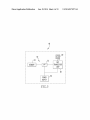
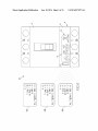
FIG. 6 is a schematic diagram of a circuit interrupter
system 62 according to another alternative exemplary
embodiment of the present invention. Circuit interrupter sys
tem 62 includes a con?gurable circuit interrupter 4 as
described elsewhere herein and a number of con?guration
card devices 64. In the illustrated embodiment, three con?gu
ration card devices 64 (labeled 64A, 64B and 64C) are shown.
It will be understood, however, that three con?guration card
devices 64 is meant to be exemplary only, and that circuit
interrupter system 62 may employ more or less than three
con?guration card devices 64. As used herein, the term “con
?guration card device” shall refer to a pocket-sized card hav
ing a housing made of, for example, plastic, and an embedded
integrated circuit. Each of the con?guration card devices 64 is
preprogrammed with certain stored con?guration informa
tion (e.g., predetermined functional trip settings) for the cir
cuit interrupter 4, and, as described in detail below, is struc
tured to transmit its stored con?guration information to
Jun. 19, 2014
information to be transferred (the con?guration information,
e.g., the functional trip settings) is embedded (e.g., via modu
lation) in the radiated near-?eld. That radiated near-?eld will
induce a ?eld in NFC coupling element 30 of electronic trip
unit 8 (which is within the radiated near-?eld). The induced
?eld is provided to NFC transceiver chip 28, which converts
it back into digital information (i.e., functional trip settings)
that may be used by microprocessor 18. The transferred func
tional trip settings are stored in the non-volatile memory
portion of NFC transceiver chip 28 and, in the exemplary
embodiment, in EEPROM 24 foruse by microprocessor 18 as
described elsewhere herein (i.e., by the trip unit program). In
the exemplary embodiment, feedback (e.g., in the form of a
blinking LED or some other suitable form) is provided to the
user when the con?guration steps as just described have been
successfully completed.
electronic trip unit 8 over an NFC interface between the
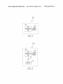
[0050] FIG. 8 is a schematic diagram showing certain
selected components of con?guration card device 64 (labeled
64-2) according to an alternative exemplary embodiment.
con?guration card device 64 and electronic trip unit 8 in order
to con?gure electronic trip unit 8. As seen in FIG. 6, in the
Con?guration card device 64-2 of this embodiment includes
an NFC transceiver chip 66 coupled to an NFC coupling
illustrated embodiment, each of the con?guration card
element 68 as described above. The non-volatile memory
devices 64A, 64B and 64C stores a different set of predeter
portion of NFC transceiver chip 28 stores the con?guration
information associated with con?guration card device 64-2.
mined functional trip settings. In addition, each con?guration
card device 64 may be labeled with (e. g., printed thereon) the
predetermined functional trip settings associated therewith
and/ or information identifying the circuit interrupter 4.
[0048] FIG. 7 is a schematic diagram showing certain
selected components of con?guration card device 64 (labeled
64-1) according to one exemplary embodiment. Con?gura
tion card device 64-1 of the present embodiment includes an
NFC transceiver chip 66 (similar to NFC transceiver chip 28
described herein) coupled to an NFC coupling element 68
(similar to NFC coupling element 30 described herein). The
non-volatile memory portion of NFC transceiver chip 28
stores the con?guration information associated with con?gu
In addition, as seen in FIG. 8, con?guration card device 64-2
of the present embodiment includes an on-board power sup
ply in the form of a battery 70 that is selectively coupled to
NFC transceiver chip 66 by a manually operated switch 72.
Thus, con?guration card device 64-2 is con?gured to operate
as an active NFC device, with power being provided to NFC
transceiver chip 66 via actuation of switch 72. As a result, in
this embodiment, it is not necessary for electronic trip unit 8,
and thus circuit interrupter 4, to have auxiliary power in order
for the con?guration information associated with con?gura
tion card device 64-2 to be transferred to electronic trip unit 8
over the NFC interface. Instead, power for NFC transceiver
card device 64-1 is con?gured as a passive NFC device.
chip 28 of electronic trip unit 8 will be transferred thereto
(along with the stored con?guration information) over the
NFC interface when con?guration card device 64-2 is
brought into proximity with electronic trip unit 8 and switch
Furthermore, as described below, in this embodiment, elec
72 is actuated.
ration card device 64-1. In addition, as seen in FIG. 7, con
?guration card device 64-1 of the present embodiment does
not include an on-board power supply, and thus con?guration
tronic trip unit 8 functions as an active NFC device and
[0051] Thus, in circuit interrupter system 62, employing
provide the power needed by con?guration card device 64-1
either con?guration card devices 64-1 or 64-2, a number of
to con?guration card device 64-1 over the NFC interface
different con?guration card devices 64 (each programmed
with different con?guration information) may be provided to
between the two devices. As will be appreciated, this requires
electronic trip unit 8, and thus circuit interrupter 4, to have
auxiliary power.
a user, such as a maintenance person, and the user may select
?gure electronic trip unit 8 using the con?guration informa
one of the con?guration card devices 64 to con?gure circuit
interrupter 4 as needed. Alternatively, a service provider, such
as the provider of the circuit interrupter 4, may provide a user
tion associated with con?guration card device 64-1, the user
with an appropriately programmed con?guration card device
brings con?guration card device 64-1 into close proximity
64 as needed to con?gure circuit interrupter 4.
[0049]
In particular, in operation, when it is desired to con
with electronic trip unit 8. Con?guration card device 64-1 is
brought close enough to allow for a near-?eld coupling inter
face to be established between electronic trip unit 8 and
con?guration card device 64-1 (e.g., within 4 cm or less).
When this is done, the RF near-?eld being radiated by NFC
coupling element 30 of electronic trip unit 8 will induce a ?eld
in NFC coupling element 68 of con?guration card device
64-1, which is used to provide power to NFC transceiver chip
66. In response, NFC transceiver chip 66 will cause the stored
con?guration information to be transferred to electronic trip
unit 8 over the NFC interface between the two devices. In
particular, NFC transceiver chip 66 will cause NFC coupling
element 68 to radiate an RF near-?eld in a manner wherein the
[0052]
Moreover, the above exemplary embodiments have
been described in connection with an electrical distribution
system that includes a circuit interrupter wherein con?gura
tion information is provided to and/or read from the circuit
interrupter using near-?eld communications. It will be under
stood, however, that the concepts of the present invention are
not limited to circuit interrupters, but rather may be employed
with other types of electrical distribution systems that include
other types electrical devices or components that require con
?guration information to be provided to and/or read from the
electrical device or component. For example, such electrical
devices or components may include, without limitation, a
metering device, a monitoring device, a control device, or any
US 2014/0170971A1
component forming part of a switchgear, which as is known,
Jun. 19, 2014
equipment.
[0056] As is known in the art, when a breaker, such as
circuit interrupter 4', trips, it can be for several reasons. Each
reason has different implications for the servicing electrician.
In addition, while a breaker, such as circuit interrupter 4', is
[0053]
power-?ow is valuable for diagnosing other problems. Thus,
is a combination of electrical disconnect switches, fuses or
circuit breakers used to control, protect and isolate electrical
FIG. 9 is a schematic diagram of a circuit interrupter
system 74 according to yet another alternative exemplary
embodiment of the present invention. Circuit interrupter sys
tem 74 includes a con?gurable circuit interrupter 4' and a
portable computing device 76.
[0054]
Circuit interrupter 4' is similar to circuit interrupter
4 and includes an operating mechanism 6 as described else
where herein. Circuit interrupter 4', however, includes a
modi?ed electronic trip unit 8' that is similar to electronic trip
unit 8 in all respects except that it further includes a display
device 78, which in the exemplary embodiment is an LCD. In
one aspect, electronic trip unit 8' is structured and con?gured
(by way of one or more routines stored in RAM 22 and
executable by microprocessor 18 of electronic trip unit 8') to
cause display device 78 to display data relating to the opera
tion and/or status of circuit interrupter 4' in the form of a
two-dimensional (2D) barcode 80, such as, without limita
tion, a standard Datamatrix barcode (see FIG. 10), that is
generated by electronic trip unit 8'. As described in more
detail below, portable computing device 76 is structured to
capture an image of 2D barcode 80, decode the 2D barcode 80
to obtain the data encoded therein, and display information
based on the decoded data in a user friendly format. Particular
examples of such information being encoded into 2D barcode
80 and subsequently displayed on portable computing device
76 are provided elsewhere herein following the description of
the exemplary portable computing device 76.
[0055] An exemplary portable computing device 76 that
may be used in circuit interrupter system 74 is depicted gen
erally in FIG. 9 and schematically in FIG. 11. The exemplary
portable computing device 76 may be, for example and with
out limitation, a smartphone, a tablet PC, or a laptop or
notebook PC. As seen in FIGS. 9 and/or 11, portable com
puting device 76 includes an input apparatus 82 (e.g., a key
board, a keypad, a touch screen, or some combination
thereof), a display 84, a processor apparatus 86, and a digital
camera 88 (including an image capture device such as a
CCD). A user is able to provide input into processor apparatus
86 using input apparatus 82, and processor apparatus 86
provides output signals to display 84 to enable display 84 to
display information to the user as described in detail herein.
Processor apparatus 86 comprises a microprocessor (HP) 90
(or other suitable processing device) and a memory 92 that
interfaces with microprocessor 90. Memory 92 can be any
one or more of a variety of types of internal and/or external
closed (pre-trip) and carrying normal current, data about that
communicating reasons for a trip and/or data about pre-trip
power-?ow can be very helpful to a servicing electrician to
enable him or her to quickly ?nd and ?x whatever problem
exists in the wiring or powered equipment. Accordingly, in
one exemplary embodiment, the data that is encoded into 2D
barcode 80 for display on display 78 may include one or more
of the following: (1) cause-of-trip information, including one
of: (a) Short Delay, meaning there was a large overload for a
short time (probably a piece of equipment is failing), (b) Long
Delay, meaning there was a small overload for a long time
(probably too much equipment on that circuit), (c) Ground
Fault, meaning somewhere current is ?owing to ground caus
ing a dangerous situation, and (d) Instantaneous, meaning a
catastrophic event, usually a direct short in the wires, has
occurred; (2) load information including the actual values of
the current ?owing in the three phases of the breaker, such as
circuit interrupter 4', for a certain amount to time (e.g., N
seconds) prior to trip (for example if the breaker is feeding a
three phase motor, the phases should all be roughly equal; if
one phase is off, that might indicate that something is wrong
with the motor such that it will probably fail (bum-out the
windings) or be unable to deliver the shaft power needed); (3)
voltage information including the actual measurement of
phase to phase voltages for a certain amount to time prior to
trip (much like current, an imbalance indicates problems in
the connected devices, such as, without limitation, an
upstream transformer that is failing or a downstream load that
is bad); and (4) harmonics information (all electrical devices
emit a certain amount of energy across the spectrum; exces
sive levels can cause interference in other devices; harmonics
information can be used as a diagnostic to ?x those interfer
ence problems).
[0057] FIGS. 12-15 illustrate operation of circuit inter
rupter system 74 according to an exemplary embodiment
using one particular, non-limiting example implementation
wherein cause of trip information, pre-trip power-?ow infor
mation and certain other information is transferred to and
displayed on portable computing device 76. In particular, in
the present example, electronic trip unit 8' is be con?gured to,
in the event of trip in circuit interrupter 4', create a number 2D
barcodes 80 by encoding into barcode form the following
information: (i) the cause of the trip, (ii) the values of the
current ?owing in the three phases of circuit interrupter 4'
prior to trip , (iii) con?guration settings information for cir
storage media such as, without limitation, RAM, ROM,
EPROM(s), EEPROM(s), FLASH, and the like that provide a
storage register, i.e., a machine readable medium, for data
cuit interrupter 4' that are relevant to the trip, (iv) service
related information that is relevant to the trip (described in
greater detail herein), and (v) voltage and/or current wave
storage such as in the fashion of an internal storage area of a
computer, and can be volatile memory or nonvolatile
onds) prior to trip. Depending on the capacity of the particular
memory. Memory 92 has a number of routines 94 stored
therein that are executable by microprocessor 90. One or
more of the routines 94 implement (by way of computer/
processor executable instructions) a software application that
is con?gured to decode the 2D barcode 80 to obtain the data
encoded therein, and display information based on the
decoded data on display 84 (routines 94 thus comprise a
computer program product tangibly embodied on a computer
readable medium of the portable computing device 76).
form information for a certain amount to time (e.g., N sec
2D barcode implementation that is used, that information
may be encoded in a single 2D barcode 80 or in multiple 2D
barcodes 80. Electronic trip unit 8' then causes the 2D barcode
or barcodes 80 to be displayed on display 78. In the event
multiple 2D barcodes 80 are used, the 2D barcodes 80 are
displayed in a repeating sequence.
[0058] Next, digital camera 88 of portable computing
device 76 is used to capture a digital image of each of the 2D
barcodes 80, and the software of portable computing device
US 2014/0170971A1
Jun. 19, 2014
76 as described herein is then used to decode the information
[0061] In still another particular exemplary embodiment,
contained in each of the 2D barcodes 80. Once decoded, that
information may be displayed to the user on display 84 of
electronic trip unit 8' may be con?gured to display the 2D
barcodes 80 one pixel at a time for capture by digital camera
portable computing device 76. In particular, in the present
88 of portable computing device 76 and subsequent decoding
example, referring to FIG. 12, a screen 96 is provided on
thereby. In such a con?guration, the 2D barcodes 80 would in
essence be ?ashed in a sequential pattern that could be cap
tured as a movie by portable computing device 76.
[0062] While speci?c embodiments of the disclosed con
display 84. Screen 96 includes the cause of the trip (Short
Delay in the present example) and the values of the current
?owing in the three phases of circuit interrupter 4' just prior to
trip (IA:2,000 A, IB:5,278 A and IC:3,175 A in the present
example). Screen 96 also includes buttons 98 and 100 which
may be clicked (selected) in order to cause additional infor
mation to be displayed on display 84. Speci?cally, as seen in
FIG. 13, when button 98 is selected, a screen 102 is provided
on display 84. Screen 102 includes the con?guration settings
for circuit interrupter 4' that are relevant to the Short Delay
trip. Screen 102 also includes buttons 104 and 106 which may
be clicked (selected) in order to cause additional information
to be displayed on display 84. In particular, as seen in FIG. 13,
button 104 includes a link (e.g., URL) to the user manual or a
cept have been described in detail, it will be appreciated by
those skilled in the art that various modi?cations and altema
tives to those details could be developed in light of the overall
teachings of the disclosure. Accordingly, the particular
arrangements disclosed are meant to be illustrative only and
not limiting as to the scope of the disclosed concept which is
to be given the full breadth of the claims appended and any
and all equivalents thereof.
What is claimed is:
1. An electrical distribution system, comprising:
an electrical component having a ?rst near-?eld commu
nications chip coupled to a ?rst near-?eld communica
troubleshooting guide for circuit interrupter 4'. When button
104 is selected, a pdf of the user manual troubleshooting
guide is obtained (e.g., from a remote sever) and is displayed
tions coupling element; and
an electronic device having a second near-?eld communi
cations chip coupled to a second near-?eld communica
tions coupling element, wherein the electronic device is
on a screen 108 on display 84 as shown in FIG. 14. In addi
tion, in the present example, button 106 includes a link to
contact information for a service electrician or the like for
structured to transmit ?rst information to the ?rst near
circuit interrupter 4', which, when selected, will cause that
contact information to be displayed on display 84. Referring
?eld communications chip and/ or receive second infor
mation from the ?rst near-?eld communications chip
over a near-?eld communications interface established
again to FIG. 12, when button 100 is selected, a screen 110
shown in FIG. 15 is provided on display 84. Screen 110
includes voltage waveforms for circuit interrupter 4' for a
certain amount to time (e.g., N seconds) prior to trip.
between the ?rst near-?eld communications coupling
element and the second near-?eld communications cou
pling element.
2. The system according to claim 1, wherein the electronic
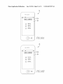
[0059] FIGS. 16A-16B illustrate operation of circuit inter
rupter system 74 according to an alternative exemplary
device is a portable handheld electronic device having a
power supply, wherein the electronic device is structured to
embodiment wherein current and/ or voltage information for
provide power to the ?rst near-?eld communications chip
the three phases of circuit interrupter 4' is transferred to and
displayed on portable computing device 76 in near real time.
In particular, in this embodiment, electronic trip unit 8' is
over the near-?eld communications interface such that the
?rst information may be transmitted to the ?rst near-?eld
communications chip and/ or the second information may be
received from the ?rst near-?eld communications chip over
the near-?eld communications interface when the electrical
con?gured to repeatedly and periodically (e.g., without limi
tation, once every second) create a 2D barcode 80 that has
encoded therein the then current phase current values and/or
phase voltage values for circuit interrupter 4'. In the illustrated
example, phase current values are employed. Each 2D bar
code 80 is displayed on display 78 until it is replaced with the
next, updated 2D barcode 80, and so on. Thus, someone such
as a service technician or electrician can use digital camera 88
of portable computing device 76 to capture a digital image of
each of the 2D barcodes 80 as they are sequentially generated.
The captured images may then be sequentially decoded and
used to create sequential screens 112 shown in FIGS. 16A and
16B (and so on) which display the phase currents of circuit
interrupter 4' on a near real time basis. As such, portable
computing device 76 is able to operate as a near real time
meter for circuit interrupter 4'. As will be appreciated, rather
than sequentially encoding and displaying phase current val
ues as in the illustrated example, other types of information,
such as phase voltage values and phase current or voltage
waveforms, may be sequentially encoded and displayed as
just described.
[0060] According to a further particular exemplary
embodiment, portable computing device 76 may be con?g
component does not have auxiliary power.
3. The system according to claim 2, wherein the electronic
device is structured to transmit the ?rst information to the ?rst
near-?eld communications chip over the near-?eld commu
nications interface when the electrical component does not
have auxiliary power, and wherein the ?rst information com
prises con?guration information for the electrical compo
nent.
4. The system according to claim 3, wherein the electrical
component is a circuit interrupter, and wherein the con?gu
ration information comprises functional trip settings for the
circuit interrupter.
5. The system according to claim 3, wherein the electrical
component is a metering device, a monitoring device or a
control device.
6. The system according to claim 2, wherein the electronic
device is structured to receive the second information from
the ?rst near-?eld communications chip over the near-?eld
communications interface when the electrical component
does not have auxiliary power, and wherein the second infor
mation comprises at least one of stored con?guration infor
captures to another (e.g., remotely located) computer system
mation for the electrical component and diagnostic informa
tion relating to the operation and/or status of the electrical
for further analysis and/ or storage/record keeping.
component.
ured to transmit the images of the 2D barcodes 80 that it
US 2014/0170971A1
Jun. 19, 2014
7. The system according to claim 6, wherein the electrical
component is a circuit interrupter, wherein the stored con
?guration information comprises functional trip settings for
?eld communications chip over the near-?eld communica
tions interface when the electrical component does not have
comprises at least one of a cause of trip, pre-trip current
auxiliary power, and wherein the ?rst information comprises
con?guration information for the electrical component.
16. The method according to claim 15, wherein the elec
information, pre-trip voltage information and harmonics
trical component is a circuit interrupter, and wherein the
the circuit interrupter, and wherein the diagnostic information
information.
8. The system according to claim 1, wherein the electronic
con?guration information comprises functional trip settings
device is a metering module, wherein the metering module is
for the circuit interrupter.
17. The method according to claim 15, wherein the elec
structured to receive the second information from the ?rst
near-?eld communications chip over the near-?eld commu
trical component is a metering device, a monitoring device or
nications interface, and wherein the metering module is struc
18. The method according to claim 14, wherein the method
includes receiving the second information from the ?rst near
?eld communications chip over the near-?eld communica
tions interface when the electrical component does not have
auxiliary power, and wherein the second information com
prises at least one of stored con?guration information for the
tured to calculate power or energy information.
9. The system according to claim 1, wherein the electronic
device is a con?guration card device storing the ?rst infor
mation, the ?rst information being con?guration information
for the electrical component, wherein the electronic device is
structured to transmit the ?rst information to the ?rst near
?eld communications chip over the near-?eld communica
tions interface.
10. The system according to claim 9, wherein the con?gu
ration card device includes a power supply selectively con
nectable to the second near-?eld communications chip,
wherein the con?guration card device is structured to provide
power to the ?rst near-?eld communications chip over the
near-?eld communications interface such that the ?rst infor
mation may be transmitted to the ?rst near-?eld communica
tions chip over the near-?eld communications interface when
the electrical component does not have auxiliary power.
11. The system according to claim 9, wherein the electrical
component is a circuit interrupter, and wherein the con?gu
ration information comprises functional trip settings for the
circuit interrupter.
12. The system according to claim 9, wherein the electrical
component is a metering device, a monitoring device or a
control device.
13. A method of transferring information in an electrical
distribution system having an electrical component having a
?rst near-?eld communications chip coupled to a ?rst near
?eld communications coupling element and an electronic
device having a second near-?eld communications chip
coupled to a second near-?eld communications coupling ele
ment, comprising:
establishing
a near-?eld
communications
interface
between the ?rst near-?eld communications coupling
element and the second near-?eld communications cou
pling element; and
performing at least one of: (i) transmitting ?rst information
to the ?rst near-?eld communications chip over the near
?eld communications interface, and (ii) receiving sec
ond information from the ?rst near-?eld communica
tions chip over the near-?eld communications interface.
14. The method according to claim 13, wherein the elec
tronic device is a portable handheld electronic device having
a power supply, wherein the method includes providing
power to the ?rst near-?eld communications chip over the
near-?eld communications interface such that the ?rst infor
mation may be transmitted to the ?rst near-?eld communica
tions chip and/or the second information may be received
from the ?rst near-?eld communications chip over the near
?eld communications interface when the electrical compo
nent does not have auxiliary power.
15. The method according to claim 14, wherein the method
includes transmitting the ?rst information to the ?rst near
a control device.
electrical component and diagnostic information relating to
the operation and/or status of the electrical component.
19. The method according to claim 18, wherein the elec
trical component is a circuit interrupter, wherein the stored
con?guration information comprises functional trip settings
for the circuit interrupter, and wherein the diagnostic infor
mation comprises at least one of a cause of trip, pre-trip
current information, pre-trip voltage information and har
monics information.
20. The method according to claim 13, wherein the elec
tronic device is a metering module, wherein the method
includes receiving the second information from the ?rst near
?eld communications chip over the near-?eld communica
tions interface, and wherein the metering module is structured
to calculate power or energy information.
21. The method according to claim 13, wherein the elec
tronic device is a con?guration card device storing the ?rst
information, the ?rst information being con?guration infor
mation for the electrical component, wherein the method
includes transmitting the ?rst information to the ?rst near
?eld communications chip over the near-?eld communica
tions interface.
22. The method according to claim 21, wherein the con
?guration card device includes a power supply selectively
connectable to the second near-?eld communications chip,
wherein the method includes providing power to the ?rst
near-?eld communications chip over the near-?eld commu
nications interface such that the ?rst information may be
transmitted to the ?rst near-?eld communications chip over
the near-?eld communications interface when the electrical
component does not have auxiliary power.
23. The method according to claim 22, wherein the elec
trical component is a circuit interrupter, and wherein the
con?guration information comprises functional trip settings
for the circuit interrupter.
24. The method according to claim 22, wherein the elec
trical component is a metering device, a monitoring device or
a control device.
25. A method of con?guring an electrical component hav
ing a ?rst near-?eld communications chip coupled to a ?rst
near-?eld communications coupling element:
providing a con?guration card device having a second
near-?eld communications chip coupled to a second
near-?eld communications coupling element, the con
?guration card device storing con?guration information
for the electrical component;