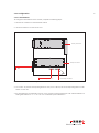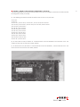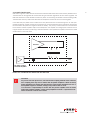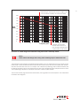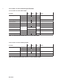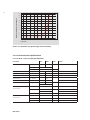
1
NSG 5600
Hardware guide
601-303C
NSG 5600
Hardware guide
Contents
1
Safety instructions
1.1 Classification of dangers
1.2 Warning symbols on the Test System
1.3 Excess voltage category
1.4 Range of validity
1.5 Safety of operation
1.6 Personnel
1.7 Responsibility for safety precaution
1.8 Safety regulations
1.9 Reduction of operational safety
1.10 As agreed use
1.11 General instructions
1.11.1 Electrical safety
1.11.2 Safety testing
1.12 Installation
1.13 Test execution
1.14 Dangers concerning the generator
1.15 Dangers concerning the DUT
2Introduction
2.1 NSG 5600 overview
2.2 NSG 5600 automotive conducted immunity EMC standard types
2.2.1 Supply voltage variations (SVV)
2.2.1.1 Pulse 4c (Pulse 4)
2.2.1.2 Pulse 4d
2.2.1.3 Pulse 2b
2.2.1.4 Pulses CI260, CI250A, fuel pump transient (FPT)
2.2.2 Power magnetics (PM)
2.2.2.1 Helmholtz coil
2.2.2.2 Radiating loop
2.2.3 Conducted sine waves (CSW)
2.3 NSG 5600 system configuration
3Installation
3.1
Checking the shipment
3.2 Delivery contents
3.3 Operating position
3.4 Line voltage connection and grounding
3.4.1 Mains voltage selector
3.5 Installation/set-up NSG 5600
3.5.1 The interlock connector
3.6 Installation/set-up controller module CT 5610
3.6.1 Handling & safety
3.6.1.2 Handling
3.6.1.3 General module protection
3.6.2 Configuration
3.6.2.1 GPIB address
3.6.2.2 CAN address
7
8
8
9
9
9
9
9
10
10
10
10
11
11
12
13
13
14
15
15
16
16
16
16
16
16
16
17
17
17
17
19
19
19
19
19
20
23
24
24
24
24
24
25
25
26
3.6.3 Installation
3.6.4 Verification
3.7 Installation / set-up function generators FG 5620 / FG 5621 (option)
3.7.1 Handling & safety
3.7.1.2 Handling
3.7.2 Configuration
3.7.2.1 Setting the FG 5620 CAN address
3.7.2.2 Setting the FG 5621 CAN address
3.7.2.3 FG 5620 / FG 5621 module configuration in multiple FG card systems
3.7.3 Installation
3.7.4 Verification
3.8 Installation / set-up DC switch module DS 5630 (option)
3.8.1 Handling & safety
3.8.1.1 Storage and transport
3.8.1.2 Handling
3.8.1.3 General module protection
3.8.3 Installation
3.8.4 Verification
3.9 Installation / set-up power amplifier module PA 5640 (option)
3.9.1 Handling & safety
3.9.1.2 Handling
3.9.1.3 General module protection
3.9.2 Installation
3.8.4 Verification
3.10 Installation / set-up transformer coupler module TC 5650 (option)
3.10.1 Handling & safety
3.10.1.1 Storage and transport
3.10.1.2 General module protection
3.10.2 Installation
4Operation
4.1 NSG 5600 basic chassis
4.1.1 Basic chassis overview
4.1.2 Basic chassis types
4.1.3 NSG 5600 chassis components
4.1.3.1 Backplane
4.1.3.2 Modules
4.1.3.3 Blanking panels
4.1.3.4 On/off switch
4.1.3.5 Auxiliary interface card
4.1.3.6 Fans
4.1.4 Chassis connectors
4.1.4.2 Interlock signals
4.2 CT 5610 digital controller module
4.2.1 Introduction
4.2.2 Functional description
4.2.2.1 Carrier card
4.2.2.2 Microprocessor card
4.2.3 Connector pin-outs
4.2.3.1 Connector IEEE 488: 24 way
4.3 FG 5620/ FG 5621 function generator modules
4.3.1 Introduction
4.3.2 Functional description
4.3.3 FG 5620 module pin assignments
NSG 5600
27
28
28
28
28
29
29
30
31
37
38
39
39
39
39
39
40
40
41
41
41
41
41
42
42
42
42
43
43
44
44
44
45
46
46
46
46
46
46
47
47
49
50
50
51
51
51
52
53
54
54
55
57
4.3.3.1 15 way D-Sub female
4.3.3.2 SMB socket SM
4.3.3.3 SMB socket RF
4.3.4 Using the arbitrary waveform memory
4.4.1 Introduction
4.4.2 Functional description
4.4.3 Connectors
4.5 PA 5640 power amplifier module
4.5.1 Introduction
4.5.2 Functional description
4.5.3 Connectors
4.6 TC 5650 conducted sine waves module
4.6.1 Introduction
4.6.2 Functional description
4.6.3 Connectors
5Maintenance
5.1 Cleaning the equipment
5.2 Moving and storing the device
5.3 Protection/fuses
5.4 Declaration of conformity (CE)
6
Technical specifications
6.1 Measures and weight
6.2 Environmental conditions
6.3 Basic chassis technical specifications
6.3.1 Auxiliary signals timing diagram
6.4 CT 5610 technical specifications
6.5 FG 5620 / FG 5621 technical specifications
6.5.1 FG 5620 / FG 5621 main output
6.5.2 FG 5620 / FG 5621 auxiliary output
6.5.3 FG 5620 / FG 5621 general
6.6 DS 5630 technical specifications
6.6.1 DS 5630 - Pulse 4c path specifications
6.6.2 DS 5630 - Pulse 4d path specifications
6.6.3 DS 5630 - Pulse 2b path specifications
6.6.4 DS 5630 - General specifications
6.7 PA 5640 technical specifications
6.7.1 CSW application specifications
6.7.2 Power magnetics application specifications
6.7.3 Supply voltage internal application specifications
6.7.4 General specifications
6.8 TC 5650 technical specifications
7Addresses
58
58
58
59
60
61
62
63
63
64
66
67
67
68
69
70
70
70
71
74
75
75
75
76
77
77
78
78
78
79
82
82
83
84
85
91
91
91
93
94
95
100
6
NSG 5600
1 Safety instructions
DANGER!
It is imperative that you read the following safety instructions and all safety instructions in the manuals of connected peripheral systems before installing and
starting this test system for the first time.
DANGER!
The electrical and mechanical safety equipment must not be removed, put out of
operation or bypassed. Handle all safety equipment with care. If a safety device
should be broken or is not working, the system must be put out of operation until
the safety device is repaired or exchanged and fully in working order again.
DANGER!
The NSG 5600 is used primarily to control amplifiers. The settings in Autostar of
the gain of the amplifier must be closely observed and the output of the amplifier
tested with these settings. Failures to set, or set correctly, these parameters can
result in the amplifier being driven to maximum voltage.
These operating instructions form an integral part of the equipment and must be available to the operating
personnel at all times. All the safety instructions and advice notes are to be observed.
7
8
1.1 Classification of dangers
The safety instructions in this manual are classified in different levels. The table below shows a survey over
the relation of symbols (ideograms) and signal words to the specific risk and the (possible) consequences.
Warning symbol
Signal word
Definition
DANGER!
Possibly dangerous situation, that may cause damage
to persons or heavy damage to the tester and/or the
equipment
CAUTION!
Situation, that may cause damage to the tester and/or
the equipment
NOTE!
User tips and other important or useful information and
comments
Table 1-1: Classification of dangers
1.2 Warning symbols on the Test System
Different warning symbols are placed on the test system. The following table shows the assignment of symbols
and signal words to the specific risk.
Warning symbol
Signal word
Definition
DANGER!
Warning of voltages that might involve the risk of
electric shock
CAUTION!
Warning of a danger spot (refer to the documentation)
Table 1-2: Warning symbols on the Test System
Caution symbol
Definition
Warning of voltages that might involve the risk of electric shock
Warning of a danger spot (refer to the documentation)
Table 1-2: Warning symbols on the Test System
NSG 5600
1.3 Excess voltage category
The test system NSG 5600, as described in this manual, is related to the excess voltage category II according IEC 60664.
1.4 Range of validity
These instructions are valid for the complete installation. Further safety regulations for components installed
in this test system or additional installed devices are not suspended by these instructions.
1.5 Safety of operation
Reliable function and safe operation of the test equipment are ensured only if the relevant general precautions
as well as all safety instructions given in this manual are observed. In particular, observe the following:
Connect the generator only to line voltage that confirms to the power specification given on the type label
(on the back of the test system).
Do not touch any conductive parts at the test point connectors, the fixture and the test object during a test
run.
Never apply external voltage to the system’s output connectors.
Disconnect the generator from the mains before opening the casing for maintenance, repair or exchange
of modules.
Check that the voltage selector on the back panel of the system is set to the correct position, refer to
chapter 3.4.1 Mains voltage selector.
For power magnetics, the user is recommended to keep a safe distance from the system while in operation.
During operating the generator always observe the relevant rules of ESD (Electro Static Discharge) protection.
To guarantee the EMC features of the NSG 5600, the control computer must meet the requirements of the
EN 50082, 55011, 61000 standard.
The operation of radio equipment or other high frequency emitting devices near the DUT or adaptation
cables, may possibly lead to wrong test results (while HF energy is emitted).
Observe the environmental conditions as described in chapter 6.2 Environmental conditions.
1.6 Personnel
The generator may be operated by qualified personnel only. It may be opened for adjustment, maintenance
or repair by authorized staff only. Teseq or its representative may not be held responsible for service not
performed by Teseq personnel.
1.7 Responsibility for safety precaution
The owner, operation supervisor and/or operator of the equipment are responsible for safety. The owner,
operation supervisor and/or operator are in charge of any safety measures that do not directly concern the
generator itself. For details, see the relevant accident prevention regulations. See also the safety instructions
in the manufacturer’s manual included with any additional instrument or device you intend to use with your
Teseq equipment.
Neither Teseq nor any of the sales organisations can accept any responsibility for personal, material or consequential injury, loss or damage that results from improper use of the equipment and accessories.
9
10
1.8 Safety regulations
According to the EN 50191 standard, this equipment may involve the risk of electric shock. The owner, operation supervisor and/or operator are responsible to build-up and operate the equipment according to the
EN 50191 standard. Conductive parts must not be touched, and the test station must have appropriate warning
labels and signs. In general, observe the industrial health and safety standards pertaining to electrical test
installations in your country.
The construction of the equipment conforms to the safety requirements of IEC 348 and provides all the
prerequisites for safe and reliable operation.
Development and manufacture is in compliance with ISO 9001.
The equipment conforms to the safety requirements of IEC 1010-1/EN 61010-1 (Safety requirements for electrical equipment for measurement, control and laboratory use). The switching power supply conforms to
IEC 950.
All mains driven types of generators are equipped for high voltage working safety in accordance with
VDE 0104.
The EMC compatibility has been tested with EN 61326 version 03/2002.
1.9 Reduction of operational safety
If you have any reasons to suppose that the test equipment is not completely safe, you must shut it down and
put it out of operation. Moreover, you must mark or label the equipment appropriately so it will not inadvertently
be put into operation again. You should then call authorized service personnel for assistance.
1.10 As agreed use
The tester may be used exclusively for simulation of automotive EMC events.
1.11 General instructions
CAUTION!
Use of the generator is restricted to authorised and trained specialists.
The generator is to be used only for the purposes set down by the manufacturer. It is the user’s responsibility
to ensure that the test set-up does not emit excessive radiation that may effect other equipment.
DANGER!
The construction of the unit renders it unsuitable for use in an explosive atmosphere.
NSG 5600
DANGER!
Persons fitted with a heart pacemaker must not operate the instrument nor
approach the test rig while it is in operation.
Only approved accessory items, connectors, adapters, etc. are to be used to ensure safe operation.
1.11.1 Electrical safety
The NSG 5600 system is fitted with protective panels and covers that fully enclose any electrical mechanisms
to reduce the risk of direct contact with live parts that may harm the user during normal use. The NSG 5600
system is clearly labelled for electrical safety:
WARNING!
LETHAL DANGER THROUGH HIGH VOLTAGE. DO NOT OPEN. NO USER SERVICABLE
PARTS INSIDE. SERVICE WORK TO BE CARRIED OUT ONLY BY FACTORY TRAINED
PERSONNEL.
Picture 1–1: Electrical warning label on the rear side of the NSG 5600
1.11.2 Safety testing
The following safety precaution label specifies that the NSG 5600 system is tested to safety standards. The CE
mark label is situated on the rear of the system, which states that the system meets the European Economic
Community requirements.
Picture 1–2: CE mark label on the rear side of the NSG 5600
11
12
1.12 Installation
The instrument conforms to protection class 1.
Local installation regulations must be respected to ensure the safe flow of leakage currents.
DANGER!
Operation without a protective earth connection is forbidden!
Operate the equipment only in dry surroundings. Any condensation that occurs must be allowed to evaporate
before putting the equipment into operation. Do not exceed the permissible ambient temperature, humidity
or altitude. This equipment must not be used in an enclosed space that would restrict the air flow through
the instrument.
Use only legally approved connectors and accessory items. The instrument must be powered from a mains
supply that provides a properly earthed mains socket. Before the unit is powered up, check that the voltage
selector on the instrument is set to the correct position. It is important that there is 0 V difference of potential
between «neutral» and «ground» on the power plug for all instruments in the test, and that all instruments use
the same mains source and ground. Due to complex mains wiring and grounding in many EMC labs, failure
to observe these may result in instrument damage or unsafe conditions when the various instruments are
connected together.
The instruments must not in principle be opened. This may only be undertaken by a qualified specialist if specifically instructed to do so in the operating manual. Since the equipment generally works with two independent
power supplies for the generator and the DUT, the instrument must first be disconnected from both sources
before any changes are made. Besides the mains supply itself, certain instruments also operate at high voltages
which are not provided with any internal form of extra protection against being touched.
Ensure that all unused slots are blanked off before powering up.
NSG 5600
1.13 Test execution
The test area must be so organised that no unauthorised persons have access during execution of a test.
DUTs, together with their accessories and cables, are to be considered as being live during a test.
The test generator must be stopped and the DUT supply interrupted before any work is carried out on the
DUT.
DANGER!
The DUT is to be tested only in a protective cage or under a hood which provides
protection against electric shock and all manner of other dangers pertaining to
the particular DUT (see dangers concerning the DUT).
CAUTION!
The safety instructions concerning all the instruments and associated equipment
involved in the test rig are to be observed.
CAUTION!
The configuration of the test rig is to be strictly in compliance with the methods
described in the relevant standard to ensure that the test is executed in a standard
conforming manner.
1.14 Dangers concerning the generator
DANGER!
Local burning, arcing, ignition of explosive gases in the event of DUT failure.
DANGER!
Danger from the resultant DUT supply current caused by a flashover or breakdown
resulting from the superimposed high voltage effects.
DANGER!
Dangers from a disrupted DUT.
DANGER!
Disturbance of unrelated electronics, telecommunications, navigational systems
and heart pacemakers through unnoticed radiation of high frequency energy.
13
14
1.15 Dangers concerning the DUT
DUTs are often simply functional samples that have not previously been subjected to any safety tests. It can
therefore happen that in some cases that the DUT is quickly damaged by internal overloads caused by the
control electronics being disrupted or it may even start to burn.
CAUTION!
As soon as the DUT shows signs of being disrupted the test must be stopped and
the power to the DUT switched off.
DANGER!
Internal disruption of the electronics can result in the interference voltage or the
DUT supply voltage being present on the DUT‘s housing.
CAUTION!
Electrical breakdown or arcing from and in plugged connections that are overstressed voltage-wise during the test.
DANGER!
Explosion of electronic components with fire or fragmentation as a result of the
energy dissipated, e.g. from the resultant supply current or ignition of vaporised
plastics materials.
CAUTION!
Faulty behaviour by the DUT, e.g. robot device strikes out, temperature controller
fails, etc.
NSG 5600
2INtroduction
15
2.1 NSG 5600 overview
The NSG 5600 system performs EMC immunity testing for the automotive market and complements the
NSG 5500 system. Emphasis has been placed on the modularity of the NSG 5600 to facilitate the configuration
of a variety of systems. This solid platform allows for further system expansion and future developments.
Computer
AutoStar control software
NSG 5500
Conducted transients
NSG 5600
Supply voltage variations
Conducted sine waves
Power magnetics
Digital scope capture
PA 54840
(other sources)
Battery simulation
Supply voltage variations
Picture 2–1: System modules
System modules are housed in a chassis, providing power and inter-module interaction. A control module
provides communication between system modules and a remote PC. Modules are front mounted in the
chassis, which provides the operator with easy access to all controls.
Autostar software is a testmanagement platform, which controls the NSG 5500, NSG 5600 and a variety of
Sources, combining them into one system. In a uniform environment, Autostar provides predefined test
parameters, test sequencing, autoconfiguration, reporting in Word and storage of user-defined tests. Test
waveforms are displayed graphically and a facility exists for the capture of waveforms from a digital oscilloscope. For more details refer to the Autostar software manual.
The NSG 5600 can be operated as a free-standing system or cabinet mounted. Four basic configurations are
offered which are described in chapter 2.3 NSG 5600 system configuration.
16
2.2 NSG 5600 automotive conducted immunity EMC standard types
2.2.1 Supply voltage variations (SVV)
Supply Voltage Variations are voltage variations of the battery supply caused by engine cranking, alternator
ripple, battery charging, jump start etc. There are several types of supply voltage variation pulses and these
are categorised by Schaffner as:
2.2.1.1 Pulse 4c (Pulse 4)
4c pulses are those arbitrary waveforms that can be built up using sine, square, triangle, exponential,
Clone™ and ramp wave segments
The majority of SVV tests are of type 4c
The “c” refers to the customization of pulse 4 pulses available from the NSG 5600 system.
2.2.1.2 Pulse 4d
4d pulses are known as dips and drops
A dip is a fast (~1 μs) change form one DC level to another DC level.
A drop is a dip to 0 V
It is difficult to achieve a 1 μs rise and fall time using an amplifier. Thus two DC sources and a fast semicon ductor switch are used to achieve the required rise and fall time specs.
2.2.1.3 Pulse 2b
Pulse 2b is defined in SAEJ1113/11 and ISO 7637-2
Pulse 2b is created using a series of segments, like 4c, but requires additional control over the pulse
impedance in some cases. For example, SAEJ1113/11 requires the pulse to have an impedance of 0.5 to
3 Ω. Before the pulse and after the pulse has fired the impedance should be < 0.01 Ω.
Pulse 2b is caused by transients from DC motors which act as generators after the ignition is switched
off.
2.2.1.4 Pulses CI260, CI250A, fuel pump transient (FPT)
Some 4c type pulses (special pulses) cannot be generated using the standard waveform segments (sine,
square, triangle, ramp), which is generally due to the high speed or short duration of the pulse.
To generate these pulses the particular wave pattern is created as a bit pattern and clocked out at high
speed.
2.2.2 Power magnetics (PM)
Power magnetics are low frequency magnetic fields generated by devices such as electric motors and also
from external mains (50 Hz) sources.
Frequency range is 10 Hz to 100 kHz.
Magnetic field density is from 180 dBpT at the fundamental frequency to ~52 dBpT at the highest frequency
where 0 dBpT = 1 picoTesla (pT) = 7.96 10 -7 A/m.
The test requirements generally follow the frequency spectrum of a square wave at the fundamental
frequency.
The ability to perform these tests depends on the amplifier and coil used.
There are 2 test methods used for generating the magnetic fields:
NSG 5600
2.2.2.1 Helmholtz coil
With this method it is only necessary to know the current through the loop, because a Helmholtz coil sets
up a uniform magnetic field within a defined region for a given current.
2.2.2.2 Radiating loop
A small loop of wire is used to produce the magnetic field. A loop sensor may be fitted to it during calibration
and the magnetic field strength read back.
The DUT is marked off into small areas and the radiating loop is moved around the DUT.
Less expensive than the Helmholtz coil and particularly useful if the DUT is large.
2.2.3 Conducted sine waves (CSW)
Conducted Sine Waves are low amplitude sinusoids, which are superimposed upon the DC battery.
Frequencies from 30 Hz to 250 kHz.
Due to the high frequency nature of the sine waves it may not be possible to generate them using a DC
amplifier, instead they are generated separately and transformer coupled to the battery using an isolation
transformer.
2.3 NSG 5600 system configuration
The NSG 5600 includes the minimum system requirements to operate:
CT 5610 Digital controller module
FG 5620 (single arb card)
Additional components are available for the NSG 5600, which provide extra pulse test functionalities:
DS 5630 DC switch module
PA 5640 Power amplifier module
TC 5650 Transformer coupler module for conducted sine waves
Multiple arb cards (2, 3 or 4 Arbs) e.g. FG 5621
CT 5610
TC 5650
CSW output
Trafo
SVV internal output
PA 5640
FG 5620
PM output (coil)
DC source 1
2b
Control
SVV output
DC source 2
Switch
Protection &
monitoring
DS 5630
Picture 2-2: Functional block diagram of the NSG 5600 system
24
17
18
Customer systems can be configured by ordering from the following list of items:
NSG 5601 Basic mainframe chassis
INA 5601 TC / CSW Transformer coupler upgrade
NSG 5602 Mainframe chassis with TC / CSW
FG 5620 Function generator for arbitrary waveforms with 1 FG card
FG 5621 Function generator for arbitrary waveforms with 2 FG cards
INA 5621 FG card upgrade kit
DS 5630 DC switch module
PA 5640 Power amplifier module
TC 5650 Transformer coupler for CSW
There are four basic types of system configurations, which are as follows:
1. Voltage variation configuration (VV)
NSG 5601 / CT 5610 / FG 5620 / Autostar software / internal/external power amplifier
2. Power magnetics configuration (PM)
NSG 5601 / CT 5610 / FG 5620 / DS 5630 / PA 5640 / Autostar software / internal/external power amplifier
3. Conducted sine wave configuration (CSW)
NSG 5602 / CT 5610 / FG 5620 / DS 5630 / PA 5640 / TC 5650 / Autostar software / internal/external power
amplifier
4. Dips and drops configuration (DD)
NSG 5601 / CT 5610 / FG 5620 / DS 5630 / Autostar software / internal/external power amplifier
NSG 5600
3Installation
3.1 Checking the shipment
Upon receiving the shipment, first check the packaging and outer equipment cover for visible damage. Also,
check packaging and casings of peripherals (if you ordered any). Record in writing any defects which were
possibly caused in transit. If the shipment shows damage or is not complete, immediately advise the shipping
agency and/or your dealer.
3.2 Delivery contents
The standard delivery contains the NSG 5600 with connection cables and the instruction manual. Optional
modules are installed in the NSG 5600 if ordered. Possibly, there is also optional equipment, e.g. computer
or printer.
3.3 Operating position
The NSG 5600 must be placed in upright position firmly and securely during operation.
3.4 Line voltage connection and grounding
DANGER!
Connect the NSG 5600 only to line voltage conforming to the power specification
given on the type label.
If the grounding is interrupted inside or outside of the equipment, the NSG 5600
will become a source of danger. Additionally, the output of the device may not
conform with the relevant test standards when the grounding of the power plug
is interrupted. Carefully observe grounding precautions. The plug on the power
cord may be replaced by qualified personnel only.
The power input of the equipment is located on the rear side of the NSG 5600 (see picture 3-1). The power
input is secured by two 6 A time-lag fuses. For details, refer to chapter 5.3 Protection/fuses.
The power plug and outlet must have grounding contacts. When the NSG 5600 is brought from cold to warm
environment, the ensuing condensation may bring about dangerous conditions.
DANGER!
The NSG 5600 may only be switched on after all parts have fully acclimatized.
19
20
3.4.1 Mains voltage selector
The mains voltage selector is a small drawer placed in the mains input / main switch module. The user can
select the regional input voltage range (110 - 120 V or 220 - 240 V) by pulling out the selector (using a small
screwdriver) and turning it. The selected voltage range is marked by the small arrow on the module that points
to the white mark at the input connector assembly.
The small bar indicates the voltage range
selected (220–240 V selection shown)
Picture 3-1: Mains voltage selector (220–240 V range selected in the picture)
NSG 5600
To select the other voltage range, proceed as follows:
DANGER!
The NSG 5600 must be disconnected from the mains before working on the mains
voltage selector by disconnecting the power cord!
Carefully loosen the drawer from the input connector assembly using a screwdriver and turning it slightly
in both directions as shown in the picture below.
Picture 3-2: Loosen the drawer using a screwdriver
Pull out the drawer from the input connector assembly.
Picture 3-3: Pull out the drawer
21
22
Turn the drawer until the text of the desired voltage range and its arrow is on the bottom of the drawer.
Picture 3-4: Turn the drawer
Push the drawer back in...
Picture 3-5: Push the drawer back in
NSG 5600
...until it is fixed to the input connector assembly again.
Picture 3-6: Fix the drawer to the input connector assembly
Now reconnect the NSG 5600 to the mains.
3.5 Installation/set-up NSG 5600
This section outlines a brief checklist of items that should be done before the unit is powered up and put
into service. The NSG 5600 may be set up by qualified personnel only. It is imperative to observe the safety
instructions at the beginning of this manual.
Check that all items and accessories ordered have been delivered.
Inspect the equipment for damage during transit. Any damage found should be reported to the carrier
immediately.
Carefully study the documentation and operating instructions supplied.
The mains voltage selector on the rear of the instrument must agree with the local mains voltage (mains
frequency: 47 - 63 Hz)
Connect the mains cable to a mains outlet that has a good earth connection.
Ensure that all modules are inserted correctly and screwed home tightly.
Observe, and adhere to, the polarity of all input and output connections.
Power up and operate according to the instructions supplied.
23
24
3.5.1 The interlock connector
CAUTION!
AutoStar will not properly communicate with the NSG 5600 if the Interlock connector is not fitted.
Connect the Interlock connector to the plug labelled “INTERLOCK” on the rear side of the NSG 5600.
Picture 3-7: The interlock connector on the rear side of the NSG 5600
3.6 Installation/set-up controller module CT 5610
3.6.1 Handling & safety
3.6.1.1 Storage and transport
The CT 5610 module is preinstalled in the NSG 5600 system upon delivery. If an exchange is required, a module
can be ordered separately and it is shipped individually in a transparent static shielding bag and box.
3.6.1.2 Handling
ATTENTION!
Observe precautions for handling electrostatic discharge sensitive devices.
3.6.1.3 General module protection
The CT 5610 digital controller module meets the safety guidelines in the IEC 1010 standard.
NSG 5600
3.6.2 Configuration
25
3.6.2.1 GPIB address
To change the GPIB address of the module, complete the following steps:
1. Remove the module from the NSG 5600 chassis.
2. Locate DIP switch S1 on the carrier card.
96 way connector
96 way connector
IEEE
S1
S2
BZ1
CAN 6 way DIP switch
CAN 8 way DIP switch
Picture 3-8: CT 5610 Module top view with DIP switches S1 and S2
3. For a “HIGH” bit, set the corresponding switch to ”OFF”, for a ”LOW” bit, set the corresponding switch to ”ON”.
Switch 1 is the LSB.
4. For GPIB address 9, set switches 2 and 4 to “OFF” and the remaining switches to “ON”. Default address is 9.
Setting IEEE address 9 : 9 = 1 + 8 = 20 + 23. The default system address is 9.
26
1
1
ON
ON
S1
S2
Picture 3-9: Switch S1 - GPIB address
5. Ensure that the system configuration utility in Autostar coincide’s with the hardware address change. Refer
to the AutoStar user manual for details on the system configuration utility.
3.6.2.2 CAN address
To change the CAN address of the CT 5610 module, complete the following steps:
1. Remove the card from the NSG 5600 chassis.
2. Locate DIP switch S2.
3. For a ”HIGH” bit, set the corresponding switch to ”OFF”, for a ”LOW” bit, set the corresponding switch to “ON”.
Switch 1 is the LSB.
1
ON
S2
Picture 3-10: Switch S2 - CAN address
4. Setting CAN address 0A : 10 = 2 + 8 = 21 + 23. Thus switches 2 and 4 are turned “OFF”. (An internal pull-up
sets a bit “HIGH” when the switch is set to the “OFF” position).
5. To delete the application firmware set all switches to “OFF”.
NSG 5600
3.6.3 Installation
To install the CT 5610 in the chassis the following steps should be performed;
1. Before removing the module from it’s packaging or handling it, observe anti-static procedures.
2. Turn off the system and disconnect from mains before installing/replacing the module.
3. Slide the module carefully on the guide rails in the right-most slot of the NSG 5600 chassis.
4. Push the 96 way DIN 41612, type C plug securely into the mating socket on the backplane.
5. The module should be pushed firmly home and screwed in using the 4 collar screws mounted to the front
panel of the CT 5610 module.
Picture 3-11: CT 5610 Module installed in the right-most slot in the basic chassis
27
28
3.6.4 Verification
After inserting the CT 5610 module, power on the chassis. The green and amber LEDs on the front panel of
the CT 5610 module should flash for a few seconds while the system is initialising and the green LED should
remain on. Any IEEE communication will result in amber LED flashing briefly.
LED colour Red Amber Green LED function
Lights continuously, only when there is a fault.
Flashes to indicate an IEEE command being received/sent.
Flashes rapidly when the board is initialising / resetting.
Lights continuously, only when the board is ready to receive an IEEE
command. Flashes rapidly when the board is initialising / resetting.
Table 3-1: LED functions
NOTE!
If the green LED is not illuminated, this indicates “NO POWER“ to the card.
NOTE!
The CT 5610 may require up to 10 seconds to boot. No software communications
will be available until the “Ready“ LED is illuminated and the other LEDs have
stopped blinking. Please wait until the CT 5610 is completely initialized before
starting AutoStar.
3.7 Installation / set-up function generators FG 5620 / FG 5621 (option)
3.7.1 Handling & safety
3.7.1.1 Storage and transport
The FG 5620 module is preinstalled in the NSG 5600 system upon delivery. If an upgrade is required, an
INA 5621 can be ordered separately and it is shipped individually in a transparent static shielding bag and box.
Refer to document ISO 702-0126 «ARB 5220 / ARB 5221 module configuration in multiple arb card systems».
Normally this upgrade will be performed by local service staff.
3.7.1.2 Handling
ATTENTION!
Observe precautions for handling electrostatic discharge sensitive devices.
3.7.1.3 General module protection
The FG 5620 / FG 5621 Function generator modules meet the safety guidelines in the IEC 1010 standard.
NSG 5600
3.7.2 Configuration
29
3.7.2.1 Setting the FG 5620 CAN address
Before installing the FG 5620, the CAN address must be set. A cut-out has been designed on the solder side
of the FG 5620 carrier card to allow easy access for the user to set the CAN addresses.
1. Locate the 4 way DIP switch on the solder side of the FG 5620 carrier card, refer to picture 3-12.
96 way connector
1 2 3 4
15 way connector
SMB sockets
FG 1 LED
FG carrier card
(motherboard)
Picture 3-12: FG 5620 solder view showing the 4 way DIP switch
NOTE!
On some older versions of the FG (ARB) cards the switch used is numbered differently. Therefore, picture 3-13 should be used as a reference to determine SW1...
SW4 positions.
2. Using a screwdriver, press the appropriate DIP switch within the 4 way DIP switch to set the CAN
address.
3. When the DIP switch is pressed in, the DIP switch is ”ON” and the CAN Address is set.
The table below shows the CAN Addresses and the DIP switch to set.
30
SW1
SW2
SW3
SW4
Address
ARB1
MASTER
On
Off
Off
Off
1
ARB2
SLAVE1
Off
On
Off
Off
2
ARB3
SLAVE2
On
On
Off
Off
3
Table 3-2: FG 5620 4 way DIP switch CAN addresses
3.7.2.2 Setting the FG 5621 CAN address
Before installing the FG 5621, the CAN addresses of the FG cards must be set. Two cutouts have been designed
on the solder side of the FG 5621 carrier card to allow easy access for the user to set the CAN addresses. 1.
Locate the 4 way DIP switches on the solder side of the ARB 5221 carrier card, refer to picture 3-13.
96 way connector
1. Locate the 4 way DIP switches on the solder side of the ARB 5221 carrier card, refer to picture 3-13.
FG 1
4 way DIP switch
FG card 1
15 way connector
SMB sockets
FG 1 LED
FG 2
4 way DIP switch
FG 2 LED
1 2 3 4
15 way connector
SMB sockets
FG card 1
Picture 3-13: FG 5620 solder view showing the 4 way DIP switch
NOTE!
On some older versions of the FG (ARB) cards the switch used is numbered differently. Therefore, picture 3-13 should be used as a reference to determine SW1...
W4 positions.
NSG 5600
2. Using a screwdriver, press the appropriate DIP switch within the 4 way DIP switches to set the CAN
addresses.
3. When the DIP switch is pressed in, the DIP switch is ON and the CAN address is set. The table below shows
the CAN Addresses and the DIP switches to set.
SW1
SW2
SW3
SW4
Address
ARB1
MASTER
On
Off
Off
Off
1
ARB2
SLAVE1
Off
On
Off
Off
2
ARB3
SLAVE2
On
On
Off
Off
3
ARB4
SLAVE3
Off
Off
On
Off
4
Table 3-3: FG 5621 4 way DIP switch CAN addresses
3.7.2.3 FG 5620 / FG 5621 module configuration in multiple FG card systems
This document describes how to configure the FG 5620 and FG 5621 modules for operation in a multiple FG
card system.
If a user has only a FG 5620 (1 FG card in one 4 HP module) then the module should already be configured
correctly and the instructions below in section 1 are provided for reference only.
If a user has only one FG 5621 (2 individual FG cards in one 4 HP module) then the module should already be
configured correctly and the details in section 2 are provided for reference only.
If a user has one FG 5621 and one FG 5620 then the FG 5620 module shall need to be configured correctly as
detailed in section 3.
If a user has two FG 5621 modules then the second FG 5621 module (the one that plugs into the left slot) shall
need to be configured correctly as detailed in section 4.
If a user has a FG 5620 but has bought an INA 5221 upgrade then the instructions in section 5 should be
followed.
Note that anti-static procedures should always be observed when handling the FG cards and FG modules.
31
32
Section 1: Single FG 5620 module configuration (1 FG card)
The following details are provided for reference only. If the user has a single ARB 5220 then the module should
be configured correctly on receipt.
(a) The following connections should be linked on the FG carrier card, 701-0126
J6.1 to J6.2
J7.1 to J7.2
J21.1 to J21.2, J21.3 to J21.4, J21.5 to J21.6, J21.7 to J21.8, J21.9 to J21.10
J22.1 to J22.2, J22.3 to J22.4, J22.5 to J22.6, J22.7 to J22.8, J22.9 to J22.10
J23.1 to J23.2, J23.3 to J23.4
J24.1 to J24.2, J24.3 to J24.4
J25.1 to J25.2, J25.3 to J25.4
J26.1 to J26.2, J26.3 to J26.4
J27.1 to J27.2, J27.3 to J27.4
J28.1 to J28.2, J28.3 to J28.4
J29.1 to J29.2, J29.3 to J29.4
J30.1 to J30.2, J30.3 to J30.4
J31.1 to J31.2, J31.3 to J31.4
(b) On the FG card, S1 switch no. 1 should be set to “ON“ and switches 2 to 4 should be “OFF“, as per chapter
3.7.2.1 Setting the FG 5620 CAN address.
NSG 5600
Section 2: Single FG 5621 Module configuration (2 FG cards)
The following details are provided for reference only. If the user has a single FG 5621 then the module should
be configured correctly on receipt.
(a) The following connections should be linked on the FG carrier card, 701-0126
J6.1 to J6.2
J7.1 to J7.2
J21.1 to J21.2, J21.3 to J21.4, J21.5 to J21.6, J21.7 to J21.8, J21.9 to J21.10
J22.1 to J22.2, J22.3 to J22.4, J22.5 to J22.6, J22.7 to J22.8, J22.9 to J22.10
J23.1 to J23.2, J23.3 to J23.4
J24.1 to J24.2, J24.3 to J24.4
J25.1 to J25.2, J25.3 to J25.4
J26.1 to J26.2, J26.3 to J26.4
J27.1 to J27.2, J27.3 to J27.4
J28.1 to J28.2, J28.3 to J28.4
J29.1 to J29.2, J29.3 to J29.4
J30.1 to J30.2, J30.3 to J30.4
J31.1 to J31.2, J31.3 to J31.4
(b) On the master FG card, S1 switch no. 1 should be set to ”ON” and switches 2 to 4 should be ”OFF”. The
master FG card is the FG card in the upper position.
(c) On the slave FG card, S1 switch no. 2 should be set to ”ON” and switches 1, 3 and 4 should be ”OFF”. The
slave FG card is the arb card in the lower position.
Picture 3-14: Master (ARB 1 or ARB 1 and 2)
33
34
Picture 3-15: Slave (ARB 3 or ARB 3 and 4)
Section 3: FG 5621 Module and FG 5620 module configuration (3 FG cards)
If the user has a FG 5621 and a FG 5620 then the FG 5620 module shall need configuration upon receipt. The
FG 5621 module should not need configuration and should be set-up as per section 2 above.
The Master FG card should reside in the FG 5621 and the module should slot into the right position in the
chassis. See picture 3-17. The module should also contain slave 1.
The FG 5620 module should contain slave 2 and should slot into the left position in the chassis. See picture
3-17.
To configure the FG 5620 it is necessary to do the following:
(a) Remove the following links on the FG carrier card, 701-0126
J21.1 to J21.2, J21.3 to J21.4, J21.5 to J21.6, J21.7 to J21.8, J21.9 to J21.10
J22.1 to J22.2, J22.3 to J22.4, J22.5 to J22.6
J23.1 to J23.2, J23.3 to J23.4
J24.1 to J24.2, J24.3 to J24.4
J25.1 to J25.2, J25.3 to J25.4
J26.1 to J26.2, J26.3 to J26.4
J27.1 to J27.2, J27.3 to J27.4
J28.3 to J28.4
J29.3 to J29.4
J30.1 to J30.2, J30.3 to J30.4
J31.1 to J31.2, J31.3 to J31.4
(b) On the FG card, set S1 switches no. 1 and 2 to the ”ON” position and switches 3 and 4 to ”OFF”. This sets
up a CAN ID address of 3. See chapter 3.7.2.1 Setting the FG 5620 CAN address.
NSG 5600
Section 4: 2 ARB 5621 Modules configuration (4 FG cards)
If the user has two FG 5621 modules then one FG 5621 module shall need configuration upon receipt. One
FG 5621 module should be designated for the right slot and will not require configuration. The master FG
card should reside in this FG 5621 the module should also contain slave 1.
The second FG 5621 module should contain slave 2 and slave 3 and should slot into the left position in the
chassis. See picture 3-17.
To configure the second FG 5621 it is necessary to do the following:
(a) Remove the following links on the FG carrier card, 701-0126
J21.1 to J21.2, J21.3 to J21.4, J21.5 to J21.6, J21.7 to J21.8, J21.9 to J21.10
J22.1 to J22.2, J22.3 to J22.4, J22.5 to J22.6
J23.1 to J23.2, J23.3 to J23.4
J24.1 to J24.2, J24.3 to J24.4
J25.1 to J25.2, J25.3 to J25.4
J26.1 to J26.2, J26.3 to J26.4
J27.1 to J27.2, J27.3 to J27.4
J28.3 to J28.4
J29.3 to J29.4
J30.1 to J30.2, J30.3 to J30.4
J31.1 to J31.2, J31.3 to J31.4
(b) On the FG card closest to the 96w DIN41612C connector, set S1 switches no. 1 and 2 to ”ON” and switches
3 and 4 to “OFF”. This sets up a CAN ID address of 3. See chapter 3.7.2.2 Setting the FG 5621 CAN address.
(c) On the other FG card, set S1 switch no. 3 to “ON” and switches 1, 2 and 4 to “OFF.” This sets up a CAN ID
address of 4. See chapter 3.7.2.2 Setting the FG 5621 CAN address.
Section 5: Upgrading a FG 5620 to a FG 5621 using the INA 5621
If the user has a FG 5620 module (single arb system) and wishes to upgrade to a FG 5621 (dual arb system)
this can be achieved by purchasing an INA 5621 upgrade kit. The kit consists of an Arb card, an assembled
front panel and the various fixing parts needed to upgrade the FG 5620.
The following instructions should be followed when upgrading the module.
a) Get the FG 5620 module. Remove the two screws holding the front panel to the FG carrier PCB. Keep the
screws as they are needed during assembly of the FG 5621.
b) Get the 4 spacers and 4 M2.5x6 screws from the INA 5621 kit. Fit the spacers to the mounting holes as shown in
picture 3-16.
35
36
Spacers
Front panel
Fixing hole
Spacers
Picture 3-16: Spacer positions for the second FG card
c) Get the FG card from the INA 5621 kit. Set the CAN address to 2 by setting S1 switch no. 1 to “OFF” and S1
switch no. 2 to “ON”. S1 switches no.’s 3 and 4 should be “OFF”.
d) Carefully assemble the FG card to the FG 5620 carrier card. The card fits upside down with the 15w D-sub
connector facing in the same direction as the master FG card. Ensure that the card fits snugly into all of
the connectors.
e) Screw the remaining 4 M2.5x6 screws from the INA 5621 kit into the 4 spacers and gently tighten.
f) Get the assembled front panel from the INA 5621 kit. Using the 2 screws removed in step (a) above fit the
panel to the FG carrier card.
g) The 15w D-sub cable in the INA 5621 kit is for the second arb card.
h) The SMB cable assemblies and T-piece are for use in multiple arb systems. Refer to the NSG 5600 hardware
manual regarding how to connect up multiple FG cards.
NSG 5600
3.7.3 Installation
37
To install the FG module in the chassis the following steps should be performed;
1. Before removing the module from it’s packaging or handling it, observe anti-static procedures.
2. Turn off the system and disconnect it from the mains before installing/replacing the module.
3. Check if it is necessary to set the CAN address. Refer to chapter 3.7.2 Configuration.
4. Check if it is necessary to configure the FG modules in multiple FG card systems. Refer to chapter 3.7.2.3
FG 5620 / FG 5621 Module configuration in multiple FG card systems.
5. Slide the FG module carefully on the guide rails in either of the two slots to the left of the CT 5610 slot in
the NSG 5600 chassis. Refer to table 3-4 and picture 3-17.
6. Push the 96 way DIN 41612 type C connector securely into mating socket on the backplane.
7. The module should be pushed firmly home and screwed in using the 2 collar screws mounted on the front
panel of the FG 5620 or FG 5621 modules.
FG modules (5620 or 5621)
ARB1
ARB3
FG card
ARB2
ARB4
CT 5610 slot
left
slot
right
slot
Picture 3-17: Basic chassis containing 2 FG 5621 (4 ARB cards) in left and right slots
38
Picture 3-17: Basic chassis containing 2 FG 5621 (4 ARB cards) in left and right slots.
No of ARBs
FG modules
Slot
CAN Address
1
FG 5620
right/ARB1
1
2
FG 5621
right/ARB1
right/ARB2
1
2
3
FG 5621 (2 ARBs)
right/ARB1
right/ARB2
1
2
FG 5620 (1 ARBs)
left/ARB1
3
FG 5621 (2 ARBs)
right/ARB1
right/ARB2
1
2
FG 5621 (2 ARBs)
left/ARB3
left/ARB4
3
4
4
Table 3-4: Lists the no. of FG cards and their location in the chassis slots
3.7.4 Verification
A single green LED is mounted on the front panel of the FG 5620 as it has a single FG card. There are two green
LEDs on the front panel of the FG 5621 as there are two FG cards. The green LEDs are activated on the front
panel of the module when a user selects a FG card using the Autostar software.
LED colour
LED function
1
Power up system and open Autostar, each green LED flashes for a short
period. Flashes continously throughout the waveform generation.
Table 3-5: LED functions
NSG 5600
3.8 Installation / set-up DC switch module DS 5630 (option)
3.8.1 Handling & safety
3.8.1.1 Storage and transport
The DS 5630 module is preinstalled in the NSG 5600 system upon delivery. If an upgrade is required, a module
can be ordered separately and it is shipped individually in a transparent static shielding bag and box.
3.8.1.2 Handling
As the module is quite heavy (approx. 6 kg), care should be taken when removing the system from it’s box
and inserting it into the chassis.
ATTENTION!
Observe precautions for handling electrostatic discharge sensitive devices.
3.8.1.3 General module protection
Overcurrent Front panel 75 A MCB protects against current overload for supply voltage variations.
Overcurrent is indicated by Autostar. A Power “OFF/ON” is required if overcurrent
occurs.
Overvoltage Internal crowbar circuit senses overvoltage >75 volts.
Overvoltage is indicated by Autostar. A power “OFF/ON” is required if overvoltage
occurs.
Reverse connection Internal crowbar senses reverse voltages > -15 V. A power “OFF/ON” is not required
Protection action
if reverse voltage crowbar occurs.
Inductive load protection As with reverse voltage, inductive load kickback is protected against by an internal
crowbar circuit.
Overtemperature An overtemperature switch cuts out the main DC power path when the heatsink
temperature exceeds 80 degrees.
Safety The DS 5630 DC switch module meets the safety guidelines in the IEC 1010 standard.
3.8.2 Configuration
The configuration of the module, cables, inputs, etc. is explained in chapter 4.1.2 Basic chassis types and in
chapter 4.4.2 Functional description.
39
40
3.8.3 Installation
To install the DS 5630 in the chassis the following steps should be performed:
1. Before removing the module from it’s packaging or handling it, observe anti-static procedures.
2. Turn off the system and disconnect from mains before installing/replacing the module.
3. Slide the module carefully on the guide rails in the left most slot of the NSG 5600 chassis.
4. The module will align itself using the four 4 mm banana plugs on the NSG 5601 or NSG 5602 backplane.
5. The module should be pushed firmly home and screwed in using the 4 collar screws mounted to the front
panel of the DS 5630.
Picture 3-19: DS 5630 Module installed in the left-most slot in the basic chassis
3.8.4 Verification
There are two LEDs on the front panel of the DS 5630 module.
LED colour
LED function
Green
LED “ON“ if power is present in the module.
Red
LED “ON“ when an interlock error occurs.
Table 3-6: LED functions
NSG 5600
3.9 Installation / set-up power amplifier module PA 5640 (option)
3.9.1 Handling & safety
3.9.1.1 Storage and transport
The PA 5640 module is preinstalled in the NSG 5600 system upon delivery. If an upgrade is required, a module
can be ordered separately and it is shipped individually in a transparent static shielding bag and box.
3.9.1.2 Handling
ATTENTION!
Observe precautions for handling electrostatic discharge sensitive devices.
3.9.1.3 General module protection
The PA 5640 Power amplifier module meets the safety guidelines in the IEC 1010 standard.
3.9.2 Installation
To install the PA 5640 in the chassis the following steps should be performed:
1. Before removing the module from it’s packaging or handling it, observe anti-static procedures.
2. Turn off the system and disconnect from mains before installing / replacing the module.
3. Slide the module carefully on the guide rails into the slot beside the DS 5630 module in the centre of the
NSG 5600 chassis.
4. Push the 96 way and 48 way plugs securely into the mating socket on the backplane.
5. The module should be pushed firmly home and screwed in using the 4 collar screws mounted to the front
panel of the PA 5640.
41
42
Picture 3-19: DS 5630 Module installed in the left-most slot in the basic chassis
3.8.4 Verification
There are two LEDs on the front panel of the DS 5630 module.
LED colour
LED function
Red
The overtemperature LED illuminates when the temperature on the heatsink
exceeds 75°C. This will cause the output to go to zero (shutdown) and will
remain so until temperature of heatsink drops below 70°C.
Table 3-7: LED functions
3.10 Installation / set-up transformer coupler module TC 5650 (option)
3.10.1 Handling & safety
3.10.1.1 Storage and transport
The TC 5650 module is preinstalled in the NSG 5602 system upon delivery. If an exchange is required, a module
can be ordered separately and it is shipped individually in a transparent static shielding bag and box.
3.10.1.2 Handling
ATTENTION!
Observe precautions for handling electrostatic discharge sensitive devices.
NSG 5600
3.10.1.3 General module protection
The TC 5650 Transformer coupler module to switch on conducted sine waves meets the safety guidelines in
the IEC 1010 standard.
3.10.2 Installation
NOTE!
The NSG 5602 contains the necessary internal audio transformer to be used with
this module. An NSG 5602, DS 5630 and PA 5640 are required for use with this
module.
To install the TC 5650 module in the chassis the following steps should be performed:
1. Before removing the module from it’s packaging or handling it, observe anti-static procedures.
2. Turn off the system and disconnect from mains before installing/replacing the module.
3. Slide the module carefully on the guide rails into the slot between the PA 5640 module and the FG 5621
module (optional) in the NSG 5600 chassis.
4. Push the 96 way and 48 way plugs securely into the mating sockets on the backplane.
5. The module should be pushed firmly home and screwed in using the 4 collar screws mounted to the front
panel of the TC 5650 module.
Picture 3-21: TC 5650 Module installed in the basic chassis
43
44
4Operation
4.1 NSG 5600 basic chassis
4.1.1 Basic chassis overview
The basic system is housed in a 7U 84HP chassis, weighing approximately 18 to 26 kg depending whether the
system is a NSG 5601 or NSG 5602. The chassis has positions at the front for various modules to plug into a
backplane which routes the signals used by the modules.
The CAN-bus, well known in automotive technology circles is used as the system bus. The chassis contains two
power supplies and one mains transformer, which provide all of the power required by the plug-in modules.
Two mains operated fans are mounted on the rear of the chassis to aid in the cooling of the DS 5630 and
PA 5640 modules.
Chassis features:
Modular structure to system
Internal CAN bus
Standard auxiliary signals (DUT_FAIL etc.)
Interlock connector
Picture 4-1: NSG 5600 system basic chassis showing the backplane and the module guide rails
NSG 5600
4.1.2 Basic chassis types
45
NSG 5600 is a generic name used for the NSG 5601 and NSG 5602 chassis due to the similarity between them.
The NSG 5601 can be upgraded to an NSG 5602 using an INA 5601 upgrade kit (service center upgrade). The
NSG 5602 contains an audio isolation transformer, which is used during conducted sine wave testing (CSW).
The NSG 5601 has every feature the NSG 5602 has except the transformer and the mounting plate.
In the NSG 5602, DC power to the transformer is first passed from the DS 5630 through the TC 5650 (conducted sine waves) module and then to the transformer via the backplane which is to allow the transformer
be connected to the positive or negative side of the battery. The primary of the transformer is connected to
the PA 5640 or another amplifier output via the backplane. The amplifier is an integral part of the test circuit.
Irregular output will result in performing a CSW test without a low-impedance amplifier connected to “MAIN
SOURCE INPUT” on the DS 5630.
PA 5640
EUT
PA 5840 or other
external amplifier
Picture 4-2: Conducted sine waves from the NSG 5602
CAUTION!
As you can see from picture 4-2, the transformer coupling method of the CSW test
uses coupling that may not be stable with all power amplifiers. While all Teseq
power amplifiers are tested with this function, other power amplifiers are not. If
an amplifier begins to oscillate, damage may result to the DS 5630.
It is the user’s responsibility to ensure that the power amplifier used is stable
under this complex coupling. Certain Teseq amplifiers contain a “capacitive mode”
which should be used for best results.
46
4.1.3 NSG 5600 chassis components
The NSG 5600 system chassis contains a number of components, which are described as follows:
4.1.3.1 Backplane
The purpose of the backplane is to pass common signals and power between the various modules within
the NSG 5600 system. The backplane is an 84HP 6U backplane with an L-shaped cut-out. The top half of the
backplane contains positions for seven 96 way DIN 41612 type C connectors. The bottom half of the backplane
contains positions for six 48 way DIN 41612 type E connectors. Power from the DC power supplies and from
the mains transformer is brought onto the backplane to be distributed to the various modules.
4.1.3.2 Modules
The modules (CT 5610, FG 5620, FG 5621, DS 5630, PA 5640 and TC 5650) are installed in the front of the chassis.
Each module is installed by sliding it along the guide rails and slotting it into the connectors on the backplane.
For more details, refer to the appropriate module sections in this manual.
4.1.3.3 Blanking panels
Before the system is powered up ensure that all unused slots are blanked off, using blanking panels. The
blanking panels are fitted on the chassis when the user receives the system.
Picture 3-3: NSG 5500 Rear view
4.1.3.4 On/off switch
An on/off switch on the back panel is used to switch “ON” and “OFF” the system mains power.
4.1.3.5 Auxiliary interface card
The rear panel of the NSG 5600 contains an auxiliary interface card. This board provides an interface to a
number of auxiliary signals. Refer to chapter 4.1.4.1 Auxiliary interface signals description.
NSG 5600
4.1.3.6 Fans
A mains operated fan is mounted on the rear of the chassis to aid in the cooling of the modules. The fan is
4 wire device, which operates at nominally either 115 or 230 V. The speed of the fan changes as the mains
voltage changes for particular settings.
4.1.4 Chassis connectors
4.1.4.1 Auxiliary interface signals description
All auxiliary signals are isolated from any other power supply lines within the system. A “HIGH” on a signal line
corresponds to +12 V (with respect to the 0 V available on pin 1 of the 9 way D-Sub connector).
CRO_TRIG
This output signal is reserved for future use.
TESTEND
The purpose of TESTEND is to indicate when a test begins and when it ends. TESTEND goes LOW at the
start of every test and goes HIGH again at the end of the test.
– The signal for TESTEND originates on the FG card.
– TESTEND is active LOW in the NSG 5600 and is an output.
– TESTEND goes LOW <1 ms before the event and goes HIGH again <1 ms after the event.
– TESTEND is available on pin 4 of the 9 way D-Sub connector.
DUT_FAIL
The purpose of DUT_FAIL is to indicate to the NSG 5600 that a failure has occurred within the DUT (Device
Under Test).
– DUT_FAIL is thus an input.
– If the DUT has an output which indicates when the DUT fails, then this line may be used when such a
failure occurs.
– By pulling pin 5 of the 9 way D-Sub LOW (i.e. by shorting it to pin 1, 0 V) the user indicates to the NSG
5600 (and Autostar) that a failure has occurred.
Depending upon the software condition set-up the system may react in three ways:
a) Do nothing
b) Stop the test
c) Pause the test
The DUT_FAIL signal indicates a failure to the processor, not the FG card(s). Thus, a time lag is expected before
the system reacts to the DUT_FAIL. This time is <50 ms.
If the test is paused upon detection of a DUT_FAIL signal then it can be resumed either within Autostar by
pressing the pause (amber) button in the Run Time Control or by sending another active low pulse to the
auxiliary signal, as shown in chapter 6.3.1 “Auxiliary signals timing diagram.”
47
48
PAUSE_CONT
The purpose of PAUSE_CONT is to allow the user to pause a test at any time and then continue it some
time later.
– This signal is available on pin 7 of the D-Sub and is active LOW.
– When a LOW going pulse is put on this pin the system pauses the test upon detection of it. It remains
paused until another LOW going pulse is put on the pin, at which time the test shall continue. The test
resumes from the point it was paused. Thus, sending the pin HIGH does not resume the test.
– The PAUSE_CONT signal indicates a test pause to the processor, not the FG card(s). Thus, a time lag is
expected before the system reacts to the PAUSE_CONT. This time is <50 ms.
EXT_TRIG
The purpose of EXT_TRIG is to allow the user to start a test externally.
– This signal is available on pin 6 of the 9 way D-Sub.
– If a user wishes to start a test with an external signal, the external trigger option must first be enabled
in Autostar.
– The test may be then set-up to run as normal. However, if the external trigger feature is enabled, then the
system will not begin the test until the EXT_TRIG signal goes LOW. After it goes LOW the test begins as
normal. While waiting for the external trigger event, Autostar will display a waiting for external trigger
message.
– Once a test has started with EXT_TRIG LOW, pulling it HIGH does nothing as the system ignores any
further state transitions.
– The EXT_TRIG signal indicates a test start to the processor, not the FG card(s). Thus, a time lag is expected
before the system reacts to the EXT_TRIG. This time shall not be <50 ms.
Pin assignment
The pin-out of the 9 way auxiliary D-Sub connector is as follows:
Pin
Signal
1
0 V Aux
2
+12 V Aux
3
CRO_TRIG
4
TESTEND
5
DUT_FAIL
6
EXT_TRIG
7
PAUSE_CONT
8
NC
9
NC
Table 4-1: 9 way D-Sub connector pin-outs
NSG 5600
5 4 3 2 1
9 8 7 6
4.1.4.2 Interlock signals
The rear panel of the NSG 5600 contains an auxiliary interface card. This board provides an interface to one
15 way D-Sub Interlock connector. All interlock signals are isolated from any other power supply lines within
the system.
The function of Interlock is to provide a safety mechanism for the user during normal operation.
To ensure system operation pins 1 and 5 must be linked on the ‘Interlock’ D-Sub connector. If the connection is missing the test running shall stop (or not commence) and all output connections shall be disabled.
A LOW indicates an interlock error. A red LED on the DS 5630 module indicates that an interlock error has
occurred.
The signal INTERLOCK1 returns from the Auxiliary Interface card to the processor. The system reacts immediately to an interlock error, whereas a short delay may be expected before the software reacts to the interlock
error. This delay should not exceed 100 ms.
CAUTION!
AutoStar will not properly communicate with the NSG 5600 if the Interlock connector is not fitted.
The pin-outs of the 15 way D-Sub Interlock connector is as follows:
Pin
Signal
Function
1
0 V INT
2
Interlock IN linked to Interlock
NC
3
Interlock IN linked to Interlock
Microprocessor GND
4
Interlock IN linked to Interlock
NC
5
Interlock IN linked to Interlock
Interlock signal to microprocessor
6
Interlock IN linked to Interlock
NC
7
Interlock IN linked to Interlock
NC
8
Interlock IN linked to Interlock
NC
9
Interlock IN linked to Interlock
NC
10
Interlock IN linked to Interlock
NC
11
Interlock IN linked to Interlock
NC
12
Interlock IN linked to Interlock
NC
13
Interlock IN linked to Interlock
NC
14
Interlock IN linked to Interlock
NC
15
Interlock IN linked to Interlock
NC
Table 4-2: 15 way D-Sub Interlock connector pin assignment
49
50
4.2 CT 5610 digital controller module
4.2.1 Introduction
The CT 5610 digital controller module has been designed to meet the high performance levels achievable
with the NSG 5600 system. This module is the central controller for the NSG 5600 system and is capable of
controlling up to 4 function generator cards over the internal CAN bus, as well as all other NSG 5600 modules
in the system. One controller is required in each test system.
Picture 4-4: CT 5610 controller module
The CT 5610 module is capable of controlling all test system resources over a single IEEE address. The CT 5610
module controls all the addressing, real-time and synchronisation tasks on the CAN-bus as well as maintaining
communication with the PC and hence with the Autostar user software. The CT 5610 also reacts to various
auxiliary user signals such as DUT_FAIL.
NSG 5600
4.2.2 Functional description
51
The CT 5610 module consists of a carrier card and the microprocessor daughter card.
LEDs
Microcontroller &
periphery
I/O
IEEE
Interface
CAN
Interface
(internal use only)
IEEE
connector
Picture 4-5: CT 5610 Controller module functional block diagram
4.2.2.1 Carrier card
The carrier card connects to the backplane of the NSG 5600 and provides an interface from the microprocessor
card to the system. In order for the microprocessor card to operate as the main system controller, the carrier
card contains additional circuitry whose main function blocks are listed below:
CAN controller and transceiver
GPIB chipset for communication to the host PC
DIP switches for GPIB and CAN identifiers
Input and output latches
Diagnostic LEDs
All of the above functional blocks interface with the microprocessor card through two 60 pin connectors, as
per the MA module standard.
4.2.2.2 Microprocessor card
The NSG 5600 firmware resides on the microprocessor card, which is mounted on the CT 5610 carrier card.
The main function of the firmware is to provide a control interface between the NSG 5600 software and
hardware. The CT 5610 module is controlled from the PC via the high speed GPIB interface on the carrier card
and processes messages to and from the software. Up to four function generator (FG) cards can be controlled
via the CAN bus. The CT 5610 also interfaces with the DC 5630 DC switch module, the PA 5240 power amplifier
module and the TC 5650 transformer coupler module for conducted sine waves (CSW).
52
4.2.3 Connector pin-outs
READY LED (green)
ACTIVE LED (amber)
FUALT LED (red)
IEEE 488 24 pin connector
Picture 4-6: CT 5610 Module front panel connector
NSG 5600
4.2.3.1 Connector IEEE 488: 24 pin
Pin no.
Signal name
1
DIO1N
2
DIO2N
3
DIO3N
4
DIO4N
5
EOIN
6
DAVN
7
NRFDN
8
NDACN
9
IFCN
10
SRQN
11
ATNN
12
DGND
13
DIO5N
14
DIO6N
15
DIO7N
16
DIO8N
17
RENN
18
DGND
19
DGND
20
DGND
21
DGND
22
DGND
23
DGND
24
DGND
Table 4-3: 24 pin IEEE connector
53
54
4.3 FG 5620/ FG 5621 function generator modules
4.3.1 Introduction
The function generator modules for arbitrary waveform functions are used universally throughout the system
5600 for the control of sources. The FG 5620 function generator module is designed to provide the various
types of supply voltage variation (SVV) signals required for the automotive industry. This high-performance
component of the NSG 5600 system, combined with Autostar software, meets all industry standard SVV
requirements.
Picture 4-7: FG 5620 Function generator module for arbitrary waveforms
All the generators used are programmed separately in the Autostar software and operate synchronously. The
FG 5621 is a function generator module for arbitrary waveforms with two FG cards, which operate in synchrony.
Each NSG 5600 system can house from one to four FG cards by selecting the type of module required. For
example three FG cards require one FG 5621 module and one FG 5620.
NSG 5600
4.3.2 Functional description
55
The FG 5620 is a double M-module sized FG card, which is mounted on a carrier card. The FG card has built-in
standard arbitrary waveform segments (sine, square, triangle, exponential and ramp) and a large memory
capacity for waveforms, which cannot easily be defined by these standard waveform segments.
External
analog signals
LEDs
CAN
NVRAM
Waveform
generation
Main
output
Isolated
output
Microprocessor &
memory
Auxiliary
output
ILim
output
Measurement
Backplane
connector
Clock
generation
Control
logic
Picture 4-8: FG 5620 Module functional block diagram
Using Autostar, the operator can quickly and easily build up any combination of the standard segment types
(Pulse 4c) or select one of the built-in special waveform types required in the industry. Alternatively, by choosing a waveform from the built-in standards database, the operator can simply “click and play”. Refer to the
Autostar software user manual for more details on the standards database.
Each waveform can consist of up to 100 segments, with each segment effectively independent from any
other. Segments may be inserted at any point within a waveform, allowing the user flexibility while creating a
waveform. Segments may also be copied and moved as needed.
Each 4c segment can be of type sine, square, triangle, exponential, clone™ or ramp (ramp includes DC). The
amplitude of the sine, square and triangle segment types may be linearly ramped from one value to the next
in a continuous mode. In a similar fashion, an offset may be added to any of the three segment types and this
offset can be linearly ramped. The frequency of sine, square and triangle segments may be ramped either
linearly or logarithmically (base 10). Any combination of ramping of amplitude, offset and frequency is possible.
Other ramping options or segment types may be available upon request. Only one clone™ segment is allowed
during each test, and only in single channel mode.
56
Other wave segment features are also available as standard, including variation of the start and stop phase
angles (stop phase angle is only valid for cycle mode) and pulse width modulation (only valid for square
waves).
The ramp waveform segment allows the operator to build up segments of DC variation as required. If the
operator chooses static amplitude, then the familiar DC voltage is created; if required a linear ramp from one
DC value to another can be selected.
The duration of each segment within a waveform is programmable from 5 ms to 9999 hours (0.5 ms to 9999
hours for ramp), allowing the operator enormous flexibility over the test time. For sine, square and triangle
waveforms a cycle mode is available, allowing the operator to program a precise number of cycles of a segment.
However, the maximum frequency available in cycle mode is 4 or 5 kHz while it is 320 kHz in time mode.
NOTE!
The hardware switches automatically at max 5 kHz from cycle to time mode
during frequency sweeping. Because of this, there is a brief delay at 5 kHz during
frequency sweep.
If the operator has a waveform that cannot be programmed by Autostar, the waveform can be downloaded
from a PC into the FG card. Autostar provides the ability to capture a waveform from an oscilloscope, display
it and save it to a file. It may then be downloaded to the FG card for replay or distributed to suppliers who can
then, using the NSG 5600 and Autostar, also download and replay the waveform. This provides the Automotive
manufacturer with an easy way to detail a complex waveform. The user may also create complex waveforms
using packages such as Microsoft® Excel, MathSoft Mathcad etc. Once the output is saved as a text file, it
can be read in by Autostar and downloaded to the FG card.
Other features available to the operator are external amplitude variation (useful for (AM) amplitude modulation) and external offset adjustment (useful for generating ripple noise). With an FG 5621, one FG card can
generate an output signal, which is fed into the other FG. An isolated output is also provided if this is required
although the frequency bandwidth is reduced. An auxiliary programmable DC output is also available. This is
used for pulse 4d applications, where fast switching between two DC sources is required. Thus, one FG card
can control two DC power supplies. Finally, a programmable current limit output is provided for DC sources
that have this feature.
During Power Magnetics testing the FG 5620 receives a voltage and current readback from either a DS 5630
or PA 5640 module during operation, depending upon which application is running. It passes these values to
the CT 5610 via the CAN bus and from there back to the PC via IEEE 488.
The FG 5620 card can be configured as either a master or a slave for use in multiple FG card applications. Using
two FG 5621 modules, four synchronous FG cards are possible. Autostar supports four FG cards as standard
and the scope supports one FG card (master).
The FG carrier card provides a platform for either one or two FG cards, depending upon whether the operator
has a FG 5620 or an FG 5621. The FG 5620 module plugs into the NSG 5600 chassis, deriving power from the
backplane. There is no configuration required for the FG 5620 or FG 5621. For three or four FG cards, refer to
chapter 3.7.2 Configuration or document IS702-0126.
NSG 5600
4.3.3 FG 5620 module pin assignments
57
16w D-Sub female connector
SMB socket RF (MODULATION)
SMB socket SM (SUMMING)
ARB LED (green)
Picture 4-9: FG 5620 Front panel connectors
58
4.3.3.1 15 way D-Sub female
Pin no.
Pin name
Function
1
+ILim
-10 to +10 V output used for programming the current limit of a source
2
+Aux
-10 to +10 V output used for programming an auxiliary source in pulse
4d applications
4
+Vout
Main output from FG card
5
0V1
Reference for CroTrig and Zerocross
6
CroTrig
Goes LOW at the start of a test
7
-Vmeas
Currently unused
8
-IMeas
Currently unused
9
-ILim
Reference for +ILim
10
-Aux
Reference for +Aux
12
-Vout
Reference for +Vout
13
ZeroCross
Changes state as the main output voltage toggles above or below zero. Only valid for
zero offset waveforms
14
+Vmeas
Currently unused
15
+Imeas
Currently unused
3
11
4.3.3.2 SMB socket SM
Pin no.
Pin name
Centre
Distortion
Case
Reference
Function
Allows an external signal to be summed with the generated waveform, e.g. distortion
Table 4-5: SMB Socket SM connector pin assignment
4.3.3.3 SMB socket RF
Pin no.
Pin name
Function
Centre
Amplitude modulation
Case
Reference
Allows an external signal to control the amplitude of the generated
waveform, e.g. amplitude modulation
Table 4-6: SMB Socket RF connector pin assignment
NSG 5600
4.3.4 Using the arbitrary waveform memory
The FG card generates arbitrary waveforms by two different methods. For pulse 4c, the waveform is created
within Autostar using standard waveform segments (e.g. sine, square, triangle and ramp), Autostar then passes
the information about each segment to the instrument and the instrument acts accordingly. So, to generate
a sine wave Autostar tells the instrument that the waveform is of type sine, is of a certain amplitude and
frequency etc. It does not download the actual voltage level at each time interval into the FG card.
Complex waveforms using the scope utility are generated differently. The following limitations also apply to
the Clone™ feature. Autostar does not know (or try to determine) the mathematical representation of the
complex waveform. Instead it passes the voltage level at each point in time to the instrument. The instrument
stores these values (or bits) in NVRAM on the master FG card. The instrument then determines (based on the
duration of the waveform) how fast to clock out the stored bits.
The FG card has 80 kB (limited to 30 kilosamples) of memory reserved for complex waveform generation. The
time between 2 individual bits (known as the step resolution) can be varied (by varying the waveform time) from
80 ns to 10 s (up to 200 s at reduced accuracy). Thus, a waveform of 50 kB could have a minimum duration of
10 ms (200 ns x 50 kBytes) and a maximum duration of 50 ks (at the optimum resolution).
For most applications the user wishes to know the opposite: given a particular waveform duration the user
wishes to know whether a waveform can be generated correctly by the FG card.
For example, if the duration of a complex waveform is 5 ms then, by defining 25 kBytes of data the waveform
can be clocked out with 200 ns resolution (5 ms / 200 ns = 25 kBytes). If 200 ns resolution is not required, the
user may decide to clock out 5 kBytes of data with 1 μs resolution.
It is important to understand, however, the limitations of the 80 kB memory storage. Say a user wanted to
generate a sine wave of 80 kHz for 10 seconds (forget for a moment that this can easily be generated by
the arb card using the sine function definition as explained above). Could it be stored in the memory and
successfully replayed? The answer is No. To generate a single sine wave cycle it is generally agreed requires at
least 16 points. An 80 kHz sine wave generates 80,000 cycles every second and so generates 800,000 cycles
in 10 seconds. If each cycle is 16 bytes, this implies that 12.8 MB of memory would be needed to accurately
produce the sine wave!
It is also worth noting that at 200 ns step resolution the maximum duration of a waveform is 16 ms. This is
because 200 ns x 80 kB = 16 ms. To increase the duration requires a reduction in step resolution.
In summary, if the waveform is very fast (and therefore requires a high resolution) or of very long duration the
memory capacity of the arb card may not be sufficient to accurately replay the waveform.
NOTE!
Using Clone™ memory during a pulse 4c test is a special hardware mode that
works with only one channel. It is necessary to restart the NSG 5600 before multichannel tests may be run.
59
60
4.4 DS 5630 DC switch module
4.4.1 Introduction
The DS 5630 DC switch module is designed to provide a high power DC switch for automotive industry EMC
testing applications. This high-performance component of the NSG 5600 system combined with Autostar
software meets all industry standard DC switching requirements.
Picture 4-10: DS 5630 DC Switch module
NSG 5600
4.4.2 Functional description
The DCS 5230 module accepts two DC inputs and provides an output, which can be rapidly switched between
the two inputs. The switching parameters are controlled by the master FG card within the NSG 5600 system
and ultimately by the user through Autostar.
The module also accepts the battery input for pulse types 4c (arbitrary waveform) and 2b. For pulse 4c the
battery is simply passed from input to output with no pulse modification, while for pulse 2b the system houses
the required 2 Ω impedance that may be necessary during the pulse generation.
Pulse 2b
MAIN S. +
DC
source
Pulse 4c
BATT MAIN S. -
EUT+
EUT-
Pulse 4d
MAIN S. +
DC
source
Measurement
& protection
MAIN S. Backplane
connector
Control logic
Picture 4-11: Block diagram of DS 5630 showing 2 external sources connected to it for pulse 4d
The main battery input is fed into the 6 mm connectors labelled “Main source input“ on the front panel. For
pulse 4d applications, the second DC source should be connected to the 6 mm connectors labelled “Auxiliary
source input“ on the front panel. For all other pulse applications, other than pulse 4d, the auxiliary shorting
plug should be connected from “Auxiliary Input +“ to “Auxiliary Input -“.
The two DC source voltages are combined in the DS 5630 to provide a single output, which is brought out on
6 mm connectors labelled “EUT“ on the front panel.
The front panel also has two circuit breakers, one rated for 75 A and the other for 25 A. The 75 A MCB provides overcurrent protection in the main battery path for SVV tests while the 25 A MCB provides overcurrent
protection for CSW and PM tests. For correct operation ensure that these MCBs are switched to “ON“.
The DS 5630 provides a voltage and current readback of the battery during operation. It also has built in overcurrent, overvoltage, reverse voltage, inductive load and overtemperature protection for all pulse types.
The DS 5630 module plugs into the NSG 5600 chassis, deriving power from the backplane.
NOTE!
The measurement and protection subcircuit has approximately 20 Ω impedance.
Therefore it is not possible to provide a completely open circuit test during dips
and drops testing.
61
62
4.4.3 Connectors
Picture 4-12: DS 5630 Front panel connectors
Connector
Description
Main source +
Round 6 mm red connector
Main source -
Round 6 mm black connector
Main source + sense
Round 2 mm red connector
Main source - sense
Round 2 mm black connector
Auxiliary source +
Round 6 mm blue connector
Auxiliary source -
Round 6 mm black connector
Auxiliary source + sense
Round 2 mm red connector
Auxiliary source - sense
Round 2 mm black connector
EUT +
Round 6 mm red connector
EUT -
Round 6 mm black connector
Backplane control connector
96 way DIN 41612 type C
Blackplan power connector +
Round 4 mm red connector
Blackplane power connector -
Round 4 mm black connector
Table 4-7: DS 5630 Connector descriptions
NSG 5600
Function
These connectors connect the battery source to
the DS 5630.
These connectors connect the auxiliary source to
the DS 5630 for use in dips and drops (4d).
These connectors connect the DS 5630 to the EUT
or to the NSG 5500 battery Input, if present.
This connector connects the DS 5630 to the NSG
5600 backplane.
These connectors connect the battery to the
backplane of the NSG 5600 for use in power
magnetics and conducted sine waves.
4.5 PA 5640 power amplifier module
4.5.1 Introduction
The PA 5640 power amplifier module is designed to provide a high frequency power amplifier for particular
tests defined within the automotive industry, namely power magnetic immunity testing (PM) and conducted
sine wave testing (CSW). This high performance component of the NSG 5600 system combined with AutoStar
software meets all industry standard requirements for these tests. The PA 5640 has the same bandwidth as
the FG cards (320 kHz).
Picture 4-13: PA 5640 Power amplifier
63
64
4.5.2 Functional description
The PA 5640 module accepts an input from the master arb card within the NSG 5600 system and produces an
amplified version of the signal at one of it’s three outputs, depending upon the application chosen in Autostar.
The switching parameters are controlled by the ARB card and ultimately by the user through Autostar.
DC
source
Power
magnetics
CSW
To
coil
To audio
transformer
Amp Input
from FG card
Diff.
Amp
SVV internal
Imeas
Vmeas
Picture 4-14: Basic block diagram of the PA 5640
If CSW testing is being performed, then the output of the PA 5640 is fed to the primary of an audio isolation
transformer, in accordance with the standards defined within the industry. The transformer couples the
amplifier output (usually a sine wave) onto the secondary of the transformer, which usually have a DC source
attached. Thus a sinusoidal ripple up to several hundred kHz can be produced on top of the DC supply.
For power magnetics testing the amplifier is used in conjunction with an external DC source and automatically
controlled using Autostar. At low frequencies the currents needed to generate the required magnetic field
density are quite large and can be met using a PA 5840 or equivalent DC source. As the frequency increases,
the currents needed to generate the required magnetic field density are lower and the PA 5640 then provides
the power source. In power magnetics mode the PA 5640 is set up as a current source rather than a voltage
source. The module also contains voltage and current readback circuitry to the FG card to allow accurate
control over these parameters. The PA 5640 can drive either a radiating loop or a Helmholtz coil, depending
upon the standard that is being tested.
NSG 5600
Depending on the loop/coil used, this region must
use an external amplifier, for example PA 5840.
200
180
160
140
120
MFD
[dBpT] 100
80
60
40
20
0
10
100
1k
10k
Frequency [Hz]
100k
1M
Limitation of the sensor.
Must be above the line to
have enough resolution to be
measured by the NSG 5600.
Picture 4-15: Power magnetics limitation using solar 9230-1 and loop sensor
NOTE!
These values will change when using other radiating loops or Helmholtz coils.
A third output on the PA 5640 is provided where the operator may only need to test up to 13.5 V at low current
(a few amps). In these situations the direct output of the PA 5640 may be used as a DC amplifier, with frequencies from DC to 320 kHz and a ±15 V 5 A output. This is achieved by selecting, within Autostar software, the
PA 5640 as the battery source. The output of the FG card is then directed along the backplane to the PA 5640.
The amplified signal appears on the output connection “Power Amplifier Output“.
The PA 5640 module plugs into the NSG 5600 chassis, deriving power from the backplane. The module does
not need to be configured.
65
66
4.5.3 Connectors
Picture 4-16: PA 5640 Front panel connectors
Connector
Description
Coil +
Round red 4 mm socket
Main source -
Round black 4 mm socket
Main source + sense
Round blue 4 mm socket
Loop sensor
Female BNC connector
Amplifier output +
Round red 4 mm socket
Amplifier output -
Round black 4 mm socket
Table 4-8: PA 5640 Front panel connectors
NSG 5600
Function
These connectors are connected to radiating
loop or Helmholtz coil in power magnetics.
This is a voltage input from the loop sensor which
is attached to the radiating loop.
These connections bring the voltage directly from
the amplifier output during SVV internal tests.
4.6 TC 5650 conducted sine waves module
4.6.1 Introduction
The TC 5650 conducted sine wave module is designed for use when conducted sine wave testing (CSW) is
required.
Picture 4-17: TC 5650 Conducted sine waves module
67
68
4.6.2 Functional description
The TC 5650 module provides an output, which is effectively the secondary of the audio transformer defined
in the CSW automotive standards. Depending upon the standard, the audio transformer secondary may be
connected to either the positive or negative side of a DC source. The TC 5650, controlled by Autostar, provides
this connection automatically. It also provides an option to switch in a 100 μF bypass capacitor, as defined in
the standards.
DC source
MAIN SOURCE
DS 5630
Audio Traf.
Power
amplifier
PA
Vmeas
P-P
Det.
Imeas
RMD-DC
DUT
Picture 4-18: Basic block diagram of the TC 5650
The TC 5650 provides a voltage and current readback to Autostar via the master arb card, during CSW tests.
These parameters are displayed on the screen in real time during the test.
The TC 5650 module plugs into the NSG 5600 chassis, deriving power from the backplane. The module does
not need to be configured.
NSG 5600
4.6.3 Connectors
69
Picture 4-19: TC 5650 Front panel connectors
Connector
Description
Function
TC Output +
Round red 4 mm socket
TC Output -
Round black 4 mm socket
These jacks connect the secondary of the audio
transformer to the DUT.
Table 4-9: TC 5650 Front panel connectors
70
5Maintenance
Under normal conditions, it does not take much effort to keep your test equipment in good working order.
CAUTION!
Protect the equipment against moisture, heat and dust.
5.1 Cleaning the equipment
To clean the equipment, use a dry, clean cloth. Never use water, any other liquid or detergent.
5.2 Moving and storing the device
The device must be installed/uninstalled only by qualified personnel. Before moving the equipment (even over
a short distance), you must first turn it off and disconnect it from the mains. Remove any fixturing devices and/
or test objects. Also, disconnect the equipment from any peripherals. For longer transit, protect the equipment
against humidity, dust and shock by proper packaging.
The equipment must be stored in upright (working) position. Make sure the equipment is protected against
humidity, dust and dirt.
Observe the environmental conditions specified in chapter 6.2 Environmental conditions.
NSG 5600
5.3 Protection/fuses
The fuses are placed in the mains voltage selector. To exchange a fuse, proceed as follows:
DANGER!
The NSG 5600 must be disconnected from the mains by disconnecting the power
cord before working on the mains voltage selector!
Carefully loosen the drawer from the input connector assembly using a screwdriver and turning it slightly
in both directions as shown in the picture below.
Picture 5-1: Loosen the drawer using a screwdriver
Pull out the drawer from the input connector assembly.
Picture 5-2: Pull out the drawer
71
72
Remove the defect fuse(s)...
The defect fuse on the side of the drawer
Picture 5-3: The fuses are placed on the sides of the drawer
...probably carefully using a small screwdriver.
Picture 4-5: Remove defect fuses
NSG 5600
Replace defect fuses by new ones.
CAUTION!
Use the following fuse types
5 x 20 mm, 6 A, time-lag
Take care to install the drawer to the correct voltage range when reinstalling the
drawer into the input connector assembly.
Push the drawer back in...
Picture 5-5: Push the drawer back in
...until it is fixed to the input connector assembly again.
Picture 5-6: Fix the drawer to the input connector assembly
Now reconnect the NSG 5600 to the mains.
73
74
5.4 Declaration of conformity (CE)
NSG 5600
6Technical Specifications
6.1 Measures and weight
Dimensions: 19“ desktop housing (rack mountable),
height 330 mm (13“), depth 510 mm (20“)
Weight: NSG 5601 18 kg (no modules fitted)
NSG 5602 26 kg (no modules fitted)
6.2 Environmental conditions
Temperature range: operation at +10 to +40°C
storage at -10 to +60°C
Humidity: 30 to 75% (non condensing)
Air pressure:
860 to 1060 hPa
75
76
6.3 Basic chassis technical specifications
Parameter
Min
Max
Units
Notes
AC operating
voltage range
90
264
Volts
2 operating ranges,
100 – 120 V
220 – 240 V
Amps
2 x 6 A 20 mm fuses fitted as
standard
AC operating current
110 V
4.2
220 V
2.1
AC operating frequency
47
Control bus
CAN
Safety interlocks
Yes
DUT_FAIL
Yes
EXT_TRIG
Yes
PAUSE/RESUME
Yes
Minimum pulse width
tmin
10
EXT_TRIG to test start time
tst
PAUSE/RESUME to test pause
time
Auxiliary input signals
63
Hz
µs
Auxiliary input signals
50
ms
EXT_TRIG to test start time
tpause
50
ms
PAUSE/RESUME to test pause
time
PAUSE/RESUME to test
resume time
tresume
50
ms
PAUSE/RESUME to test
resume time
DUT_FAIL to test stop time
tstop
50
ms
DUT_FAIL to test stop time
Test start to TESTEND active
tstr
1
ms
Test start to TESTEND active
Test start to TESTEND
in-active
tstp
1
ms
Test start to TESTEND
in-active
Connectors
J1
CAN bus
J2
Unused
J3
Unused
Table 6-1: Basic chassis technical specifications
NSG 5600
6.3.1 Auxiliary signals timing diagram
77
tmin
tst
tpause
tresume
tstop
EXT_TRIG
FG output
PAUSE/RESUME
DUT_FAIL
TESTEND
tstp
tstr
Picture 6-1: Auxiliary signals timing diagram
6.4 CT 5610 technical specifications
Parameter
Module dimensions
Min
Units
Notes
Width
8
HP
1 HP = 5.08 mm
Height
6
U
1 U = 44.45 mm
Depth
170
mm
Internal control bus
CAN
IEEE 488 (GPIB)
Yes
Front panel indicators
Max
Ready
Green LED
Active
Amber LED
Fault
Red LED
Table 6-2: CT 5610 Technical specifications
Default address = 9
78
6.5 FG 5620 / FG 5621 technical specifications
6.5.1 FG 5620 / FG 5621 main output
Parameter
Output voltage
Min
Max
Units
Range
-10
+10
V
Resolution
10
mV
Accuracy
± (0.1% + 10 mV)
mV
Offset voltage
10
mV
Output impedance
10
Ω
Output current
± 100
Short circuit protection
Frequency range
Frequency resolution
Full scale settling time, 1%
mA
Yes
Sine, square,
triangle
Frequency accuracy
Slew rate
Notes
0.01
320000
Hz
Limited in cycle mode to 4 kHz
V/µs
1 k load
µs
1 k load
0.01
± (0.01% + 0.01 Hz)
-10 to 10 V
120
10 to -10 V
120
0 to 10 V
0.5
Table 6-3: Technical specifications FG 5620 / FG 5621 main output
6.5.2 FG 5620 / FG 5621 auxiliary output
Parameter
Output voltage
Min
Max
Units
Range
-10
+10
V
Resolution
10
mV
Accuracy
± (0.5% + 50 mV)
mV
Output impedance
1
Output current
± 25
Short circuit protection
Yes
Notes
Ω
mA
Table 6-5: Technical specifications FG 5620 / FG 5621 auxiliary output
NSG 5600
6.5.3 FG 5620 / FG 5621 general
79
Parameter
Min
Standard segment types
Sine, square, exponential, triangle and
ramp (including DC)
Number of segments per
waveform
1
Arbitrary waveform storage
Segment interval delay
Memory
capacity
80
Step resolution
200 ns
Max
Units
Notes
kB
30 kilosamples max.
s
Up to 200 s step resolution
possible at reduced accuracy
At a step resolution of 1s
100
1
Step accuracy
0.5
%
Time mode
200
µs
Cycle mode
0
Ramp step time
Sine, square,
triangle
5
Amplitude ramping options
Sine, square,
triangle
Linear
Offset ramping options
Sine, square,
triangle
Linear
Frequency ramping options
Sine, square,
triangle
Linear, Log10
Segment duration
Sine, square,
triangle
5
9995
Ramp
0.5
1000
All
Accuracy
ms
Does not apply to arbitrary
waveform storage types
ms
Resolution 5 ms
Resolution 0.1 ms
0.1
9999
s
Resolution 0.1 s
0.1
9999
min
Resolution 0.1 min
0.1
9999
h
Resolution 0.1 hour
1
10000
Cycles
Resolution 1 Cycle
± (1% + 1 ms)
Table 6-6: Technical specifications FG 5620 / FG 5621 general
Not applicable to cycle mode
80
Parameter
Overall test duration
Range
Min
Max
Units
1
9999
Count
345
Degrees
Notes
Continuous
Start phase angle
Stop phase angle
Square wave
duty cycle
variation
Range
Value
0
Resolution
15
Accuracy
1° or ± 2 µs
Value
15
Resolution
15
Accuracy
1° or ± 2 µs
0.01 to 160 kHz
160 to 360 kHz
Resolution
0.01 to 160 kHz
160 to 360 kHz
Accuracy
0.01 to 5 kHz
5 to 10 kHz
10 to 20 kHz
20 to 40 kHz
40 to 80 kHz
80 to 160 kHz
160 to 320 kHz
See figure 6-3
360
5
95
25
75
5
%
%
25
± 0.05
%
± 0.1
± 0.2
± 0.4
± 0.8
± 1.6
± 3.2
Rectification
Sine, square,
triangle
None, positive,
negative
Voltage distortion
Range
-10
+10
V
Frequency
DC
1
MHZ
Table 6-6: Technical specifications FG 5620 / FG 5621 general
NSG 5600
See figure 6-2
Parameter
Amplitude modulation
Connectors
Number of FG cards
Min
Max
Units
Range
-10
+10
V
Frequency
DC
1
MHz
Main output
15 Way D-sub socket
VRF
SMB socket
VSM
SMB socket
Control
3x 32 Way DIN 41612
Type C
FG 5620
1
FG 5621
2
Plugs into NSG 5600 backplane
100
Multiple FG card
synchronisation delay
Notes
ns
Event timing
Start trigger
Goes LOW at start
Module dimensions
Width
4
HP
1 HP = 5.08 mm
Height
6
U
1 U = 44.45 mm
Depth
170
mm
Type
CAN
Protocol
CANOpen
Speed
125
ID Range
1 to 15
FG 5620
1x Green LED
FG 5621
2x Green LED
Control bus
Front panel indicators
Only valid for multiple FG cards
kBits/s
0 reprogramms the NVRAM,
1 is the master FG card, 4Way
DIP switch sets the address
Table 6-6: Technical specifications FG 5620 / FG 5621 general
400
350
Start phase angle (degrees)
300
250
200
150
100
50
0
0.00
0.50
1.00
1.50
2.00
2.50
3.00
3.50
4.00
Log F (Hz)
Picture 6-2: Maximum start phase angle versus frequency
4.50
81
82
200
Minimum stop phase angle (degrees)
180
160
140
120
100
80
60
40
20
0
0.00
0.50
1.00
1.50
2.00
2.50
3.00
3.50
4.00
4.50
Log F (Hz)
Picture 6-3: Minimum stop phase angle versus frequency
6.6 DS 5630 technical specifications
6.6.1 DS 5630 - Pulse 4c path specifications
Parameter
Min
Max
Units
Range
-14
70
V
Resolution
0.1
Accuracy
± (1% + 0.2 V)
Battery input current
Range
0
Maximum DC voltage drop
IL = 75 A
Battery input voltage UB
75
A
1
V
Input to output DC resistance
Notes
mΩ
Inrush current
t = 100 ms
150
Internal quiescent current
Pulse 4c
0.01
Test duration
Range
1
9999
A
Count
Resolution 1 count
Continuous
Battery voltage readback
measurement
Ratio
0.1
V/V
Accuracy
5
%
Battery current readback
measurement
0.01 Hz to 30 kHz
30 to 300 kHz
20
3 dB BW
300
kHz
Ratio
0.1
A/A
Accuracy
5
%
Bandwidth
20
kHz
Table 6-7: Technical specifications DS 5630 - pulse 4c path specifications
NSG 5600
6.6.2 DS 5630 - Pulse 4d path specifications
Parameter
83
Min
Max
Units
Notes
60
V
See figure 6-5 for safe operating
area curve
Battery input voltage UB
Range
0
AC operating
current
Resolution
0.1
Accuracy
± (1% + 0.2 V)
Auxiliary input voltage VA
Range
0
Resolution
0.1
Accuracy
± (1% + 0.2 V)
Battery input current
Range
0
75
Auxiliary input current
Range
0
75
Battery voltage drop
IL = 75 A
UB
2
Auxiliary voltage drop
V
A
V
See figure 6-4
See figure 6-6
2
Quiescent current
VB = 60 V
3
A
Inrush current, battery and
auxiliary paths
t = 100 ms
100
A
Battery off fall time
1 kΩ load
1.5
µs
0.5
1 Ω load
Battery on rise time
1 kΩ load
5
0.2
1 Ω load
Pulse width td
Pulse interval t1
Burst interval delay
1.5
Measured directly at output
of the DS 5630. Purely resistive
load
6
Range
3µ
Resolution
1
Accuracy
± (1% + 1 µs)
Range
0.5 m
Resolution
0.1
Accuracy
± (1% + 1 ms)
Range
0
9999
s
Resolution 1 s
0
9999
min
Resolution 1 min
0
9999
h
Resolution 1 h
Accuracy
20
s
µs
20
s
ms
When ramping any parameter, t1
(min) = 1.5 ms
± (1% + 1 s)
No. of pulses per burst
1
Pulse modes
Normal or inverted
10000
Table 6-8: Technical specifications DS 5630 - pulse 4d path specifications
84
Parameter
Auxiliary voltage ramping
Min
Max
Units
Range
0
UB
V
Step size
0.1.
Notes
Overshoot
2.5
%
Settling time, 1%
50
µs
48 to 12 V dip, 10 µs pulse,
1 Ω load
1
9999
s
Resolution 1 s
1
9999
min
Resolution 1 min
1
9999
h
Resolution 1 h
1
9999
Count
Resolution 1 count
Sequence duration or
repetition
Range
Continuous
Start up delay
Accuracy
± (1% + 1 s)
Range
2s
9999
s
Resolution 1 s
2s
9999
min
Resolution 1 min
2s
9999
h
Resolution 1 h
Accuracy
± (1% + 1 s)
Table 6-8: Technical specifications DS 5630 - pulse 4d path specifications
6.6.3 DS 5630 - Pulse 2b path specifications
Parameter
Battery input voltage UA
Min
Max
Units
Range
0
UB
V
Resolution
0.01
Accuracy
Pulse 2b output impedance
± (1% + 0.2 V)
2.1 ± 10%
Pulse 2b output current
Range
End of test voltage
Range
Pulse amplitude US
Notes
Ω
25
A
0
UA
V
Range
1
UA
V
Resolution
0.01
Accuracy
± (1% + 0.2 V)
Table 6-9: Technical specifications DS 5630 - pulse 2b path specifications
NSG 5600
Parameter
Battery pulse interval time t6
Pulse width td
Battery off time t2
Pulse repetition time t1
Sequence repetition
Min
Max
Units
Range
0
UB
ms
Resolution
0.1
Accuracy
± (1% + 0.1 ms)
10 to 10%
50
Resolution
0.1
Accuracy
± (1% + 0.1 ms)
Range
2td + 50 ms 30
Resolution
0.01
Accuracy
± (1% + 0.1 ms)
Range
t 2 + 1 s or
30td
1000
Resolution
2s
9999
Accuracy
± (1% + 0.1 ms)
Range
1
5000
Notes
ms
s
s
9999
Count
Resolution 1 count
Imax
A
Imax is the maximum source
current but must be <= 25 A
Continous
Current limit
Range
0.1
Resolution
0.01
Accuracy
± (1% + 0.1 A)
Table 6-9: Technical specifications DS 5630 - pulse 2b path specifications
6.6.4 DS 5630 - General specifications
Parameter
Overcurrent protection
Min
Max
Units
Notes
A
Fast 75 A MCB
Pulse 4c, 4d
75
Pulse 2b
25
75 A MCB
0.4
5
s
Voltage sense and crowbar
Resolution
0.4
5
s
Reverse voltage diodes
Overvoltage protection
All Paths
75 ±1
V
Voltage sense and crowbar
Inductive load
l = 75 A
mH
Derate current accordingly for
increased inductive load
Reverse voltage protection
Pulse 4c
-15 ±1
V
Voltage sense and crowbar
Pulse 4d
-1
Width
40
HP
1 HP = 5.08 mm
Height
6
U
1 U = 44.45 mm
Depth
170
mm
6
kg
MCB trip time
Module dimensions
Module weight
Front panel indicators
Internal control bus
Fast 25 A MCB
300
Power
Green LED
Interlock
Red LED
Reverse voltage diodes
CAN
Table 6-10: Technical specifications DS 5630 - pulse 4c path specifications
85
86
1.80
1.60
1.40
1.20
1.00
Voltage drop (V)
0.80
0.60
0.40
0.20
0.00
0.00
10.00
20.00
30.00
40.00
50.00
Battery current (A)
Picture 6-4: Pulse 4d Battery voltage drop vs battery current
NSG 5600 Maximum load current vs battery voltage
80
70
60
50
40
IL (Amps)
30
20
10
0
0
10
20
30
40
50
60
70
VBatt (Volts)
Picture 6-5: Pulse 4d safe operating area (load current vs battery voltage)
NSG 5600
60.00
70.00
87
3.50
3.00
2.50
Quiescent current (A)
2.00
1.50
1.00
0.50
0.00
0
10
20
30
Battery voltage (V)
Picture 6-6: Pulse 4d quiescent current vs battery voltage
Picture 6-7: 13.5 V Dropout into 1 kΩ load for 10 μs
40
50
60
70.00
88
Picture 6-8: 13.5 V Dropout into 1 kΩ load for 100 μs
Picture 6-9: 13.5 V Dropout into 1 Ω load for 10 μs
NSG 5600
89
Picture 6-10: 13.5 V Dropout into 1 kΩ load for 3 μs
Picture 6-11: 13.5 V Dropout into 1 kΩ load for 5 μs
90
Picture 6-12: 13.5 V Dropout into 1 Ω load for 100 μs
NSG 5600
6.7 PA 5640 technical specifications
91
6.7.1 CSW application specifications
Parameter
Amplifier output voltage
Min
Max
Units
Notes
Range
-10
10
V
Resolution
0.2
Accuracy
± (0.01% + 0.01 Hz)
Audio transformer ratio is 2:1
so the peak voltage on the
transformer secondary is 5 V
5
A
Maximum output current at the
transformer secondary is 10 A
320
kHz
Amplifier output current
Amplifier frequency
Range
0.01
Resolution
0.001
Accuracy
± (0.01% + 0.01 Hz)
Amplifier gain
2
Table 6-11: Technical specifications CSW application
6.7.2 Power magnetics application specifications
Parameter
Extern amplifier peak output
voltage
Min
Max
Units
Range
-70
70
V
Resolution
0.1
Accuracy
Amplifier dependant
External amplifier RMS output
current
Internal amplifier peak
current
Internal amplifier peak output
current
Internal amplifier accuracy
10
A
mA
Range 1
30
1200
Range 2
1
30
Range 3
0
1
Range 1
All ranges
6
V
Notes
Rint = 5 Ω
5
Rint = 166 Ω
5
Rint = 5 Ω
± (1% + 3 µA)
Table 6-12: Technical specifications power magnetics application
92
Parameter
Amplifier frequency
Min
Max
Units
Range
0.01
>200
kHz
Resolution
0.001
Accuracy
± (0.01% + 0.01 Hz)
Internal amplifier gain
Bandwidth
Magnetic field density
1
< 5 dB
320
Range
40
Resolution
0.01
180*
Accuracy
± (1% + 0.01 Hz)
Pulse types
Sine
Step duration
1
9999
Delay between steps
1
9999
Test types
Point or sweep mode
Sweep mode step type
Linear, octave, decade
No. of test points
Point mode
1
100
Linear sweep
2
100
kHz
1 k load. All ranges
dBpT
RMS Values
Rating loop 9230-1, 0.05 m from
loop
s
Radiating loop/sensor
& helmholtz coil
Coil types
Connectors
Notes
Coil+
Red 4 mm banana
socket
Coil-
Black 4 mm banana
socket
Shield
Blue 4 mm banana
socket
Loop sensor
BNC
*Example with external loop antenna–I = ID 4)
Table 6-12: Technical specifications power magnetics application
NOTE!
The NSG 5600 supports the loop sensor that is supplied with the solar coil 9230-1
only. See figure 4-15 for limitations.
NSG 5600
6.7.3 Supply voltage internal application specifications
Parameter
Internal amplifier output
voltage
Min
Max
Units
Range
-15
15
V
Resolution
0.1
Accuracy
± (0.1% + 0.01 V)
5
Internal amplifier output
current
Magnetic field density
Range
DC
Resolution
0.01
Internal amplifier gain
Notes
A
>200
kHz
1
Offset voltage
Bandwidth
93
5
< 1 dB
320
mV
kHz
Internal amplifier gain
2
Output impedance
100
mΩ
1 k load
Slew rate
-10 to +10 V
43
V/µs
1 kΩ load
Settling time, 1%
-10 to +10 V
<1
µs
1 kΩ load
Connectors
SVV+
Red 4 mm banana
socket
SVV-
Black 4 mm banana
socket
Table 6-13: Technical specifications supply voltage internal application
94
6.7.4 General specifications
Parameter
Battery voltage readback
measurement
Min
Max
Units
Ratio
0.1
15
V/V
Accuracy
5
%
20
Battery current readback
measurement
Test duration
Notes
0.01 Hz to 30 kHz
30 to 300 kHz
3 dB BW
320
kHz
Ratio
0.1
A/A
Accuracy
5
%
Bandwidth
20
kHz
Range
1
9999
Count
Resolution
A
Fast 25 a MCB
Continous
Overcurrent protection
Module dimensions
External
25
Pulse 2b
25
Width
20
HP
1 HP = 5.08 mm
Height
6
U
1 U = 44.45
Depth
170
mm
2
kg
OverTemp
Red LED
Module weight
Front panel indicators
Internal control bus
Backplane connectors
CAN
Bus
96 way DIN 41612,
type C
48 way DIN 41612,
type E
Table 6-14: General specifications
NSG 5600
Fast 25 a MCB
6.8 TC 5650 Technical specifications
Parameter
Battery voltage
Min
Max
Units
Range
0
70
V
Resolution
0.1
Accuracy
± (1% + 0.2 V)
Maximum battery DC current
DUT AC voltage
95
25
A
15
Vpk-pk
Range
0.05
Resolution
0.01
DUT AC current
Range
0
7
ARMS
DUT output frequency
Range
10
250000
Hz
Resolution
0.01
Accuracy
± (0.01% + 0.01 Hz)
V
Transformer saturation
voltage
See figure 6-16
Standard segment types
Sine
Number of segments per
waveform
1
Segment delay
Notes
Limited to 5 kHz in cycle mode
100
Time mode
200
Cycle mode
0
µs
Amplitude ramping options
Linear
Frequency ramping options
Linear, Log10
Segment duration
5
9999
ms
Resolution 5 ms
1
9999
s
Resolution 1 s
1
6000
min
Resolution 1 min
Accuracy
Any combination of ramping
possible
1
100
h
Resolution 1 h
1
9999
Cycles
Resolution 1 cycle
± (1% + 1 ms)
Table 6-15: TC 5650 Technical specifications
Not applicable to cycle mode
96
Parameter
Min
Max
Units
Notes
Value
0
345
Degrees
Resolution 15°
Resolution
15
Accuracy
1° or ± 2 µs
Stop phase angle
Value
15
360
Degrees
Only available in cycle mode.
Resolution 15°
Internal peak to peak voltage
measurement
Range
0.05
15
V
Accuracy
± (2% + 0.1 A)
Peak to peak voltage is displayed
by Autostar during a test
Internal RMS current measurement
Range
0
ARMS
Accuracy
± (2% + 0.1 A)
RMS current is displayed by
autostar during a test
Programmable current limit
Range
0.1
Accuracy
± (10% + 0.3 A)
Start phase angle
7
7
ARMS
Bypass capacitor
100 µF ± 20%
Can be switched in or out using
AutoStar
Audio transformer
connection
Positive battery
terminal
Controlled using Autostar.
Default is positive battery
terminal
Negative battery
terminal
Module dimensions
Front panel indicators
Internal control bus
Width
8
HP
1 HP = 5.08 mm
Height
6
U
1 U = 44.45 mm
Depth
170
mm
Power
Green LED
Interlock
Red LED
CAN
Table 6-15: TC 5650 Technical specifications
NSG 5600
97
Peak to peak output voltage at 0.5 V setting
0.6
Volts p-p
0.5
0.4
1 K load
0.3
4 R load
0.2
0.1
0
10
10
100
1000
10000
100000
1000000
Log frequency [Hz]
Picture 6-13: Output voltage vs frequency for a voltage setting of 0.5 Vpk-pk at 1 kΩ and 4 Ω
loads
Peak to peak output voltage at 2 V setting
2.5
Volts p-p
2
1.5
1 K load
4 R load
1
0.5
0
0
10
100
1000
10000
100000
1000000
Log frequency [Hz]
Picture 6-14: Output voltage vs frequency for a voltage setting of 2 Vpk-pk at 1 kΩ and 4 Ω loads
98
Peak to peak output voltage at 5 V setting
6
Volts p-p
5
4
1 K load
3
4 R load
2
1
0
10
10
100
1000
10000
100000
1000000
Log frequency [Hz]
Picture 6-15: Output voltage vs frequency for a voltage setting of 5 Vpk-pk at 1 kΩ and 4 Ω
loads
Saturation voltage of TC 5650 versus frequency
Saturation Voltage (Vpp)
16
14
12
10
8
6
4
2
0
0
10
20
30
40
Frequency (Hz)
Picture 6-16: TC 5650 Transformer saturation voltage vs frequency
NSG 5600
50
60
NOTES
99
100
Headquarters
Teseq AG
4542 Luterbach, Switzerland
T + 41 32 681 40 40
F + 41 32 681 40 48
sales @ teseq.com
www.teseq.com
Manufacturer
Teseq AG
4542 Luterbach, Switzerland
T + 41 32 681 40 40
F + 41 32 681 40 48
sales @ teseq.com
China
Teseq Company Limited
T + 86 10 8460 8080
F + 86 10 8460 8078
chinasales @ teseq.com
France
Teseq Sarl
T + 33 1 39 47 42 21
F + 33 1 39 47 40 92
francesales @ teseq.com
Germany
Teseq GmbH
T + 49 30 5659 8835
F + 49 30 5659 8834
desales @ teseq.com
Japan
Teseq K.K.
T + 81 3 5725 9460
F + 81 3 5725 9461
japansales @t eseq.com
Singapore
Teseq Pte Ltd.
T + 65 6846 2488
F + 65 6841 4282
singaporesales @ teseq.com
Switzerland
Teseq AG
T + 41 32 681 40 50
F + 41 32 681 40 48
sales @ teseq.com
Taiwan
Teseq Ltd.
T + 886 2 2917 8080
F + 886 2 2917 2626
taiwansales @ teseq.com
UK
Teseq Ltd.
T + 44 845 074 0660
F + 44 845 074 0656
uksales @ teseq.com
USA
Teseq Inc.
T + 1 732 417 0501
F + 1 732 417 0511
Toll free +1 888 417 0501
usasales @ teseq.com
To find your local partner withinTeseq®’s global
network, please go to www.teseq.com
© December 2012 Teseq®
Specifications subject to change without notice.
Teseq® is an ISO-registered company. Its products
are designed and manufactured under the strict
quality and environmental requirements of the ISO
9001. This document has been carefully checked.
However, Teseq® does not assume any liability for
errors or inaccuracies.