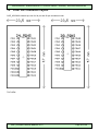
1
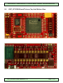
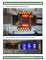
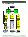
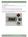
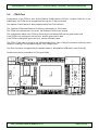
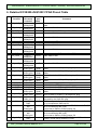
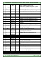
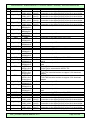
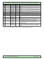
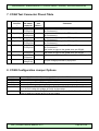
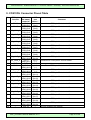
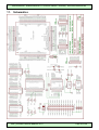
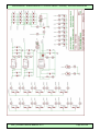
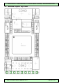
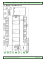
GOP_XC3S200
USER'S MANUAL
V 1.2
OHO-Elektronik
www.oho-elektronik.de
Author: M.Randelzhofer
OHO-Elektronik · Rudolf-Diesel-Str. 8 · D-85221 Dachau · Germany · www.oho-elektronik.de
OHO-Elektronik
Michael Randelzhofer
Rudolf-Diesel-Str. 8
85221 Dachau
Germany
www.oho-elektronik.de
WEB:
EMAIL: [email protected]
Phone: +49 8131 339230
FAX: +49 8131 339294
©2005-2009 OHO-Elektronik - Michael Randelzhofer
All rights reserved
Disclaimer:
Under no circumstances OHO-Elektronik - Michael Randelzhofer is liable for consequential costs,
losses, damages, lost profits.
Any schematics, pcb or program parts are under the copyright of OHO-Elektronik - Michael
Randelzhofer, and can only be reproduced by permission of this company.
The contents of this USER'S MANUAL are subject to change without notice.
However the main changes are listed in the revision table at the end of this document.
Products of OHO-Elektronik - Michael Randelzhofer are not designed for use in life support systems,
where malfunction of these products could result in personal injury.
The products of OHO-Elektronik - Michael Randelzhofer are intended for use in a laboratory test
environment or for OEM’s only. They can generate radio frequency energy (depending on the
downloaded design and application), which can disturb local radio or TV equipment, and so they have
not been tested to be CE compliant.
If you encounter any technical problems or mistakes in this document, please contact
[email protected], serious hints are very appreciated.
Trademarks:
All brand names or product names mentioned are trademarks or registered trademarks of their
respective holders.
PAL and GAL are registered trademarks of Lattice Semiconductor Corp.
GOP_XC3S200 USER'S MANUAL V1.2
Page 2 of 29
OHO-Elektronik · Rudolf-Diesel-Str. 8 · D-85221 Dachau · Germany · www.oho-elektronik.de
1. Table of contents:
1.
2.
Table of contents: .............................................................................................................................3
Introduction.......................................................................................................................................5
2.1.
GOP_XC3S200 Features:.........................................................................................................5
2.2.
GOP_XC3S200 Applications:....................................................................................................5
2.3.
Xilinx XC3S200 Features: .........................................................................................................6
2.4.
Xilinx XC3S200 Disadvantages:................................................................................................6
2.5.
GOP_XC3S200 Board Pictures,Top And Bottom View. ............................................................7
2.6.
GOP_XC3S200 Board In A Lab Environment. ..........................................................................8
2.7.
GOP_XC3S200 Board with 5 stacked OHO_DY1 modules.......................................................8
3. GOP_XC3S200 Board Overview ......................................................................................................9
3.1.
I/O Distribution ........................................................................................................................10
3.2.
Test connector ........................................................................................................................11
3.3.
JTAG Port ...............................................................................................................................12
3.4.
Power Suppy...........................................................................................................................13
3.5.
PAL / GAL Emulation Of 24 Pin And 20 Pin Devices...............................................................14
4. FPGA Design Support ....................................................................................................................14
5. About GOP_XC3S200 I/O Voltage Levels ......................................................................................15
6. Detailed XC3S200-4VQ100C FPGA Pinout Table ..........................................................................16
7. CON4 Test Connector Pinout Table................................................................................................20
8. CON2 Configuration Jumper Options..............................................................................................20
9. CON1 DIL Connector Pinout Table.................................................................................................21
10.
CON1 DIL Connector Layout ......................................................................................................22
11.
Schematics .................................................................................................................................23
12.
Module Layout Top View.............................................................................................................25
13.
Module Layout Bottom View .......................................................................................................26
14.
Technical Specifications..............................................................................................................27
15.
Literature ....................................................................................................................................28
16.
Assembly variants.......................................................................................................................29
17.
USER'S MANUAL Revisions.......................................................................................................29
GOP_XC3S200 USER'S MANUAL V1.2
Page 3 of 29
OHO-Elektronik · Rudolf-Diesel-Str. 8 · D-85221 Dachau · Germany · www.oho-elektronik.de
GOP_XC3S200 USER'S MANUAL V1.2
Page 4 of 29
OHO-Elektronik · Rudolf-Diesel-Str. 8 · D-85221 Dachau · Germany · www.oho-elektronik.de
2. Introduction
The GOP_XC3S200 is a mini module composed of an FPGA device and a configuration memory with a
PAL / GAL compatible 24 pin DIL footprint. Many additional features make it useful and flexible:
2.1.
GOP_XC3S200 Features:
XC3S200-4VQG100C FPGA, a member of the XILINX Spartan-3 family.
Xilinx XCF01S Platform Flash configuration device
Xilinx Parallel Cable IV or Platform USB Cable compatible download connector 14pin / 2mm,
an OHO-Elektronik low cost programmer is also available
4 Mbit SRAM 512k x 8, tAC = 55ns
8 Mbit user SPI FLASH
Operating voltage from 3,5V to 5.5V, switching regulator for core voltage 1,2V
Voltage translators for 5V I/O compatibility, selectable pullups to 5V
Onboard Clock oscillator with 49.152 MHz for audio or RS232 applications
2 status leds, 8 low current user leds, 2 user tact switches, 7 configuration jumper
A 9-pin test connector for probing internal signals, or interconnecting several GOP's
Reverse plug in protection, solder jumpers for additional ground connections
Easy to reuse
Professional design, manufactured on a 6 layer PCB, made in Germany
2.2.
GOP_XC3S200 Applications:
Upgrade from PAL / GAL devices, redesigns
Fast evaluation of Xilinx Spartan-3 FPGA's
Hardware platform for VHDL / VERILOG / logic design courses
Robotics
High logic density applications at tight space constraints
GOP_XC3S200 USER'S MANUAL V1.2
Page 5 of 29
OHO-Elektronik · Rudolf-Diesel-Str. 8 · D-85221 Dachau · Germany · www.oho-elektronik.de
2.3.
Xilinx XC3S200 Features:
Document [1] lists lots of goodies, here are the best facts:
Modern SRAM based 90nm 200000 Gate low cost FPGA
3840 4-input function generators, 1920 can be RAM or dual ported RAM, or shift registers
SelectRAM hierarchical memory, 12 x 18kbit Blockram, 30kbit distributed RAM
12 dedicated multipliers 18x18
4 Digital Clock Managers, DCMs
Lots of I/O standards, but GOP_XC3S200 supports LVCMOS33 and LVTTL only
Wide multiplexers, fast look-ahead carry logic, 8 global clock nets, JTAG interface with user
access
Free powerful VHDL / VERILOG / schematics / simulation design software available (Webpack)
Unlimited reprogrammability
2.4.
Xilinx XC3S200 Disadvantages:
The following items are not relevant in most cases.However, they should be used as a checklist, to query
wheather an application is affected.
No single chip solution, needs a configuration source like a platform FLASH
3 different supply voltages required: core voltage 1,2V, VCCAUX 2,5V, I/O voltage
I/Os are not 5V tolerant
High quiescent current, in the range of tens of milliamps for each of the supply voltages for
XC3S200
Design is not protected against copyright theft, configuration bitstream can be recorded
Lower performance FPGA compared to the luxury Virtex2 pro or Virtex4 FPGA's, especially not
all LUTs have RAM / shift register capabilities
DLLs in the DCM's have higher jitter than PLLs
GOP_XC3S200 USER'S MANUAL V1.2
Page 6 of 29
OHO-Elektronik · Rudolf-Diesel-Str. 8 · D-85221 Dachau · Germany · www.oho-elektronik.de
2.5.
GOP_XC3S200 Board Pictures,Top And Bottom View.
GOP_XC3S200 USER'S MANUAL V1.2
Page 7 of 29
OHO-Elektronik · Rudolf-Diesel-Str. 8 · D-85221 Dachau · Germany · www.oho-elektronik.de
2.6.
GOP_XC3S200 Board In A Lab Environment.
2.7.
GOP_XC3S200 Board with 5 stacked OHO_DY1 modules.
GOP_XC3S200 USER'S MANUAL V1.2
Page 8 of 29
OHO-Elektronik · Rudolf-Diesel-Str. 8 · D-85221 Dachau · Germany · www.oho-elektronik.de
3. GOP_XC3S200 Board Overview
2mm - 14pin
JTAG - PORT
CON3
1
XILINX
PLATFORM
FLASH
XILINX
FPGA
XC3S200
ASYNC
SRAM
512kx8
SPI
FLASH
8 MBIT
LEVEL
SHIFTER
8
USER
LEDS
1
XOSC
49.152
MHz
1,2V
Switcher
800mA
0,1" /
2.54mm
24 - Pin
DIL
SOCKET
PLUG
CON1
2,5V
Low Drop
150mA
3,3V
Low Drop
250mA
Access
To 22
FPGA
Pins
2
USER
SWITCHES
Reverse
Protection
0.3" GAP
JP1
2
14
1
13
2mm - 14pin
Jumper Block
CON2
1
JP2
JP3
9
2.54mm / 9pin
Test Connector
CON4
GOP_XC3S200 USER'S MANUAL V1.2
Solder Jumper
For Additional Ground
Connections
Page 9 of 29
OHO-Elektronik · Rudolf-Diesel-Str. 8 · D-85221 Dachau · Germany · www.oho-elektronik.de
3.1.
I/O Distribution
22 I/Os of the Xilinx XC3S200-4VQG100C FPGA are wired to a 24 pin DIL socket plug on the bottom of
the module through level shifter devices 74CB3T3245, which makes the FPGA I/Os tolerant to input
voltages up to 7V.
Pins 1, 2, 13, 21 and 23 of the DIL plug access global clock nets GCLK6, GCLK7, GCLK1, GCLK4, and
GCLK5 inside the FPGA.
These clock nets also can be used as general purpose I/Os.
Please note, that the level shifter devices reduces the ability of the FPGA I/Os to source current, but sink
current is not affected.
As an option, pullups to 5V can be enabled on pin 1 to pin 13, and pin 14 to pin 23 separately by setting
jumpers on CON2 11-12 and 13-14 respectively.
Another point to note is, that as long as the FPGA is not configured, the DIL pins are disconnected from
the FPGA, they are floating. This could be altered by RJ3.
A crystal oscillator with an output frequency of 49,152MHz is connected to GCLK0 of the FPGA. This
oscillator can be disabled completely by removing the jumper to its power supply at jumper block CON2,
position 3-4.
2 I/Os are connected to user tactile switches SW1 and SW2. SW1 is a freely available, while
SW2 also reprogramms the FPGA, if jumper CON2 7-8 is set. In this case, reprogramming the FPGA is
also possible by I/O28. Simply output a '0' on this pin, tristate otherwise.
Please do not output a '1' on this pin, because this drives a 3,3V level to the 2,5V supply by the I/O diode
at signal PROG_B.
30 FPGA I/Os are connected to an asynchronous SRAM device, organized as 512kByte x 8, with an
access time of 55ns. Due to the limited amount of I/Os of an VQ100 package, some of the SRAM I/Os
are shared with other resources of the GOP_XC3S200 module:
• 8 address lines of the SRAM are connected to 8 user leds. These leds can be enabled by jumper
CON2 9-10.
• 3 address lines of the SRAM share the SPI FLASH signals SCK, SI, SO.
It is up to the user, to care about proper multiplexing and tristating of these signals, when all affected
resources are used.
GOP_XC3S200 USER'S MANUAL V1.2
Page 10 of 29
OHO-Elektronik · Rudolf-Diesel-Str. 8 · D-85221 Dachau · Germany · www.oho-elektronik.de
3.2.
Test connector
7 I/Os are available to the front side test connector CON4.
2 I/Os are connected via level shifters (TP7, TP8) and 5 I/Os are directly connected to the FPGA (TP2,
TP3, TP4, TP5, TP6).
PLEASE NOTE:
TP2, TP3, TP4,TP5 and TP6 do not have series resistors, and so are not 5V tolerant!!!
Pin 6 of CON4 (TP6), one of the non-5V tolerant contacts, accesses global clock net GCLK2.
Pin 7 of CON4 (TP7), one of the 5V tolerant contacts, accesses global clock net GCLK3.
The test connector is primarily intended for probes of an oscilloscope or logic analyser. But since a
power supply is also provided on the connector, it is ideally suited for small hardware extensions or
debug modules like the 3-digit OHO_DY1 display module.
GOP_XC3S200 USER'S MANUAL V1.2
Page 11 of 29
OHO-Elektronik · Rudolf-Diesel-Str. 8 · D-85221 Dachau · Germany · www.oho-elektronik.de
3.3.
JTAG Port
Configuration of the FPGA is done by the Platform FLASH device XCF01S, if jumper CON2 5-6 is set.
Additionally, the FPGA can be programmed through the JTAG port as well.
The platform FLASH device is also programmed by the JTAG interface.
The 2 devices FPGA and Plattform FLASH are connected in a JTAG chain.
The FPGA is the first device in the chain, the Platform FLASH is the second.
The configuration status of the FPGA is shown by the red status led2 and the green status led1.
If the FPGA is not configured, red led2 is lit, and the green led1 is dark.
If the FPGA is configured, green led1 is lit, and the red led2 is dark.
The FPGA JTAG chain is routed to the Xilinx standard 2mm 14pin JTAG port connector CON3 by serial
resistors, enabling JTAG programming with 3,3V voltage levels.
The 2mm connector is supported by the parallel cable IV, and platform USB cables, see [2] and [3].
Please notice the pin orientation of JTAG port CON3:
GOP_XC3S200 USER'S MANUAL V1.2
Page 12 of 29
OHO-Elektronik · Rudolf-Diesel-Str. 8 · D-85221 Dachau · Germany · www.oho-elektronik.de
3.4.
Power Suppy
The module can be powered with supplies from 3.5 to 5.5 volts, since core and auxiliary voltages are
generated with on-board regulators. Standard connection for the supply is at DIL pin 24 while GND is on
pin 12 in 24 pin mode. In 20 pin mode, pin 20 is used for VCC and pin 10.for GND.
An onboard switching voltage regulator produces the FPGA core voltage of 1,2V.
The regulator [4] can source up to 800mA.
Another low drop regulator generates the VCCAUX voltage of 2,5V, sourcing up to 150mA [5].
And finally a 250mA low drop regulator is responsible for the I/O voltage of 3,3V, [6].
The module has a protection against reverse insertion, or reverse power connection. In that case, the
protection shorts the power supply by a polyfuse device. The polyfuse recovers after deactivation of the
power supply. Burn through cycles of the polyfuse are limited. For more information, please consult the
data sheet
Even so, care should be taken when plugging the module.
Consider that a short pulse of several amps can damage the environment in which the module is
inserted.
ATTENTION !!!
Please note, that a voltage above 6V on the module pins 12 and 24 will destroy the voltage regulators on
the module !!!
Especially the switching regulator is sensitive to overvoltage. Therefore, the maximum of 5,5V module
supply voltage must never be exceeded.
GOP_XC3S200 USER'S MANUAL V1.2
Page 13 of 29
OHO-Elektronik · Rudolf-Diesel-Str. 8 · D-85221 Dachau · Germany · www.oho-elektronik.de
3.5.
PAL / GAL Emulation Of 24 Pin And 20 Pin Devices
As a general hint, the modules DIL plug should be protected mechanically with an additional adaptor like
the supplied DIL sockets.
•
In 24 pin mode of the module, a 24 pin socket should be used.
•
In 20 pin mode of the module, a 20 pin socket should be used.
Please insure, that pin 1 of the module is always pin 1 of a socket.
In the 20 pin mode, an additional GND connection must be done via a 2mm jumper on jumper block
CON3 at position 1-2, see Layout Top View. This adds GND to pin 10.
For cases where additional GND connections are desired, Pins 3, 14 and 23 can be shorted to GND with
solder jumpers JP1, JP3, JP2 respectively, on the bottom side of the module. These shorts should be
soldered using a stereo microscope, to insure, that there are no other unwanted connections.
4. FPGA Design Support
VHDL and UCF design templates for 20 and 24 pin configurations are available.
GOP_XC3S200 USER'S MANUAL V1.2
Page 14 of 29
OHO-Elektronik · Rudolf-Diesel-Str. 8 · D-85221 Dachau · Germany · www.oho-elektronik.de
5. About GOP_XC3S200 I/O Voltage Levels
The Spartan3 FPGA series offer a broad variety of I/O voltage standards. However on the
GOP_XC3S200, only the LVCMOS33 and LVTTL standard is supported. This standard is required for
the level shifters [7] for conversion of 5V TTL levels as well as 5V CMOS levels. These level shifters
work bidirectional without the need of controlling their direction.
Please note, that the level shifter devices reduces the ability of the FPGA I/Os to source current, sink
current is not affected.
The level shifters introduce a delay of 0,25ns maximum.
Further on, the shifters do not clamp the outputs to their VCC of 3,3V.
They can be lifted up by pullups to a maximum of 7V.
So as an option, the GOP_XC3S200 module supports pullups to 5V or rather, the voltage at pin 24. They
can be enabled on pin 1 to pin 13, and pin 14 to pin 23 separately by setting jumpers on CON2 11-12
and 13-14 respectively.
With these jumpers enabled, the I/Os are nearly compatible to the IEE1284 standard.
So direct connection to a PC’s parallel printer port is possible.
GOP_XC3S200 USER'S MANUAL V1.2
Page 15 of 29
OHO-Elektronik · Rudolf-Diesel-Str. 8 · D-85221 Dachau · Germany · www.oho-elektronik.de
6. Detailed XC3S200-4VQ100C FPGA Pinout Table
Pin
FPGA pin
function
1
I/O_L01P_7
2
I/O_L01N_7
3
4
GND
I/O_L21P_7
5
I/O_L21N_7
6
7
8
VCCO_7
VCCAUX
I/O_L23P_7
9
I/O_L23N_7
10
11
GND
I/O_L40P_7
12
I/O_L40N_7
13
I/O_L40P_6
14
I/O_L40N_6
15
I/O_L24P_6
16
I/O_L24N_6
17
I/O-P17
18
19
20
21
VCCINT
VCCO_6
GND
I/O-P21
22
I/O_L01P_6
23
I/O_L01N_6
24
M1
25
M0
26
M2
27
I/O_L01P_5
(Schema
net name)
routed to
(IO1)
SRAM pin20
(IO2)
SRAM pin21
GND
(IO4)
SRAM pin22
(IO5)
SRAM pin23
(VCC3V3)
(VCC2V5)
(IO8)
SRAM pin25
(IO9)
SRAM pin26
GND
(IO11)
SRAM pin27
(IO12)
SRAM pin28
(IO13)
SRAM pin29
(LS6)
CON1 pin6
(LS8)
CON1 pin8
(LS5)
CON1 pin5
(LS7)
CON1 pin7
(VCC1V2)
(VCC3V3)
GND
(LS9)
CON1 pin9
(LS10)
CON1 pin10
(LS11)
CON1 pin11
(M1)
GND
(M0)
M2
CON2 pin6
(M2)
M0
CON2 pin6
(IO27)
SW1
UCF
port
name *
sa<12>
Comment
sd<0>
Sram address input A0
Led4
Sram data I/O bit0
-sd<1>
Connection to the GND Layer of the PCB
Sram data I/O bit1
sd<2>
Sram data I/O bit2
--sd<3>
LVCMOS33/LVTTL I/O Voltage 3,3V
VCCAUX must be 2,5V
Sram data I/O bit3
sd<4>
Sram data I/O bit4
-sd<5>
Connection to the GND Layer of the PCB
Sram data I/O bit5
sd<6>
Sram data I/O bit6
sd<7>
Sram data I/O bit7
pin6
(pin6)
pin8
(pin8)
pin5
(pin5)
pin7
(pin7)
---pin9
(pin9)
pin10
(pin10)
pin11
(--)
--
Connection to the 20/24pin DIL plug to pin6 via level
shifter
Connection to the 20/24pin DIL plug to pin8 via level
shifter
Connection to the 20/24pin DIL plug to pin5 via level
shifter
Connection to the 20/24pin DIL plug to pin7 via level
shifter
Internal core Voltage 1,2V
LVCMOS33/LVTTL I/O Voltage 3,3V
Connection to the GND Layer of the PCB
Connection to the 20/24pin DIL plug to pin9 via level
shifter
Connection to the 24pin DIL plug to pin10 via level shifter
Short to GND by CON2 1-2 for 20pin DIL plug
Connection to the 24pin DIL plug to pin11 via level shifter
Not used for the 20pin DIL plug
FPGA configuration mode bits
M1 is connected to GND via R2
FPGA configuration mode bits 1 = JTAG, 0 = conf. FLASH
M0 is connected to M2 via R7
Can be set to GND by CON2 jumper 5-6
FPGA configuration mode bits 1 = JTAG, 0 = conf. FLASH
M2 is connected to M0 via R7
Can be set to GND by CON2 jumper 5-6
User tact switch1, shorts IO27 to GND via 100Ω serial
resistor, needs pullup inside the FPGA
--
--
sw1
GOP_XC3S200 USER'S MANUAL V1.2
Page 16 of 29
OHO-Elektronik · Rudolf-Diesel-Str. 8 · D-85221 Dachau · Germany · www.oho-elektronik.de
28
I/O_L01N_5
(IO28)
SW2
sw2
29
30
GND
I/O_L28P_5
GND
(tp2)
-tp2
31
VCCO_5
(VCC3V3)
--
32
I/O_L28N_5
(tp3)
tp3
LVCMOS33/LVTTL I/O Voltage 3,3V
Alternatively 2,5V, selectable by solder jumper RJ1
Testconnector CON4 pin 3, not 5V tolerant !!!
33
34
VCCAUX
I/O_L31P_5
(VCC2V5)
(tp4)
-tp4
VCCAUX must be 2,5V
Testconnector CON4 pin 4, not 5V tolerant !!!
35
I/O_L31N_5
(tp5)
tp5
Testconnector CON4 pin 5, not 5V tolerant !!!
36
GCLK2
(tp6)
tp6
37
GCLK3
tp7
38
GCLK0
39
GCLK1
40
DOUT
41
42
GND
INIT
43
I/O_L30P_4
44
I/O_L30N_4
45
46
47
VCCINT
VCCO_4
I/O_L27P_4
48
DIN
49
50
I/O_L01P_4
I/O_L01N_4
51
52
53
DONE
CCLK
I/O_L01P_3
54
I/O_L01N_3
55
I/O-P17
56
57
GND
VCCO_3
(GIO37)
LS pin14
(OSC)
XOSC1 out
(LS13)
LS pin 16
CON1 pin13
(DOUT)
SRAM pin1
FLASH pin5
GND
(INIT)
XCF01 pin8
SRAM pin9
(IO43)
SRAM pin30
(IO44)
SRAM pin32
(VCC1V2)
(VCC3V3)
(IO47)
IC3 pin15
(DIN)
SRAM pin6
FLASH pin2
(IO49)
(IO50)
SRAM pin2
(DONE)
(CCLK)
(IO53)
SRAM pin3
(LS14)
CON1 pin14
(LS15)
CON1 pin15
GND
(VCC3V3)
Testconnector CON4 pin 7, not 5V tolerant !!!
This is also an input to the global clock net GCLK2
Testconnector CON4 pin 7 via level shifter
This is also an input to the global clock net GCLK3
Global clock net input GCLK0, 49,152MHz clock input
from XOSC1
Connection to the 24pin DIL plug to pin13 via level shifter
Not used for the 20pin DIL plug
This is also an input to the global clock net GCLK1
Multiple function pin
Address sa0 input for SRAM
Serial data input for FLASH
Connection to the GND Layer of the PCB
Multiple function pin
FPGA configuration FLASH reset
Address sa4 input for SRAM
"osc"
pin13
(--)
sa<0>
-sa<4>
scs
soe
--tp8
sa<2>
fcs
sa<9>
--sa<15>
pin14
(--)
pin15
(pin11)
---
GOP_XC3S200 USER'S MANUAL V1.2
User tact switch2, shorts IO28 to GND via 100Ω serial
resistor, needs pullup inside the FPGA
Jumper CON2 7-8 enables reconfiguration by SW2
Connection to the GND Layer of the PCB
Testconnector CON4 pin 2, not 5V tolerant !!!
SRAM chip select, has an external pullup, R4
SRAM output enable, has an external pullup, R1
Internal core Voltage 1,2V
LVCMOS33/LVTTL I/O Voltage 3,3V
Testconnector CON4 pin 8 via level shifter
Multiple function pin
Address sa2 input for SRAM
Serial data output from FLASH
FLASH chip select, has an external pullup, R18
Sram address input A9
Led8
FPGA configuration ready strobe, 1 = fpga configured
FPGA configuration clock
Sram address input A15
Led7
Connection to the 24pin DIL plug to pin14 via level shifter
Not used for the 20pin DIL plug
Connection to the 24pin DIL plug to pin15 via level shifter
Connection to the 20pin DIL plug to pin11 via level shifter
Connection to the GND Layer of the PCB
LVCMOS33/LVTTL I/O Voltage 3,3V
Page 17 of 29
OHO-Elektronik · Rudolf-Diesel-Str. 8 · D-85221 Dachau · Germany · www.oho-elektronik.de
58
59
VCCAUX
I/O-P59
60
I/O_L24P_3
61
I/O_L24N_3
62
I/O_L40P_3
63
I/O_L40N_3
64
I/O_L40P_2
65
I/O_L40N_2
66
67
GND
I/O_L24P_2
68
I/O_L24N_2
69
70
71
VCCINT
VCCO_2
I/O_L21P_2
72
I/O_L21N_2
73
74
GND
I/O_L01P_2
75
I/O_L01N_2
76
TDO
77
TCK
78
TMS
79
I/O_L01P_1
80
I/O_L01N_1
81
I/O-P81
82
83
84
85
GND
VCCO_1
VCCAUX
I/O_L31P_1
86
I/O_L31N_1
87
GCLK4
88
GCLK5
(VCC2V5)
(LS19)
CON1 pin19
(LS17)
CON1 pin17
(LS18)
CON1 pin18
(LS16)
CON1 pin16
(IO63)
SRAM pin4
(IO64)
SRAM pin5
(IO65)
SRAM pin7
GND
(IO67)
SRAM pin31
(IO68)
SRAM pin10
(VCC1V2)
(VCC3V3)
(IO71)
SRAM pin11
(IO72)
SRAM pin12
GND
(IO74)
SRAM pin16
(IO75)
SRAM pin15
(FTDO)
XCF01 pin4
(FTCK)
XCF01 pin6
CON3 pin6
(FTMS)
XCF01 pin5
CON3 pin4
(IO79)
SRAM pin13
(IO80)
SRAM pin14
(IO81)
SRAM pin17
GND
(VCC3V3)
(VCC2V5)
(LS20)
CON1 pin20
(LS22)
CON1 pin22
(LS21)
CON1 pin21
(LS23)
-pin19
(pin15)
pin17
(pin13)
pin18
(pin14)
pin16
(pin12)
sa<1>
swr
VCCAUX must be 2,5V
Connection to the 24pin DIL plug to pin19 via level shifter
Connection to the 20pin DIL plug to pin15 via level shifter
Connection to the 24pin DIL plug to pin17 via level shifter
Connection to the 20pin DIL plug to pin13 via level shifter
Connection to the 24pin DIL plug to pin18 via level shifter
Connection to the 20pin DIL plug to pin14 via level shifter
Connection to the 24pin DIL plug to pin16 via level shifter
Connection to the 20pin DIL plug to pin12 via level shifter
Sram address input A1
Sram write enable
sa<3>
Sram address input A3
-sa<10>
Connection to the GND Layer of the PCB
Sram address input A10
sa<5>
Sram address input A5
--sa<6>
Internal core Voltage 1,2V
LVCMOS33/LVTTL I/O Voltage 3,3V
Sram address input A6
sa<8>
Sram address input A8
-sa<17>
sa<7>
Connection to the GND Layer of the PCB
Sram address input A17
Led10
Sram address input A18
Led9
FPGA JTAG chain
FPGA TDO is connected to XCF01 TDI
FPGA JTAG chain
JTAG TCK via serial resistor to support 3,3V download
adapter
FPGA JTAG chain
JTAG TMS via serial resistor to support 3,3V download
adapter
Sram address input A7
sa<9>
Sram address input A9
sa<11>
Sram address input A11
Led3
Connection to the GND Layer of the PCB
LVCMOS33/LVTTL I/O Voltage 3,3V
VCCAUX must be 2,5V
Connection to the 24pin DIL plug to pin20 via level shifter
Connection to the 20pin DIL plug to pin16 via level shifter
Connection to the 24pin DIL plug to pin22 via level shifter
Connection to the 20pin DIL plug to pin18 via level shifter
Connection to the 24pin DIL plug to pin21 via level shifter
Connection to the 20pin DIL plug to pin17 via level shifter
Connection to the 24pin DIL plug to pin23 via level shifter
sa<18>
---
--
---pin20
(pin16)
pin22
(pin18)
pin21
(pin17)
pin23
GOP_XC3S200 USER'S MANUAL V1.2
Page 18 of 29
OHO-Elektronik · Rudolf-Diesel-Str. 8 · D-85221 Dachau · Germany · www.oho-elektronik.de
89
GCLK6
90
GCLK7
91
I/O_L31P_0
92
I/O_L31N_0
93
94
95
96
VCCINT
VCCO_0
GND
I/O_L01P_0
97
I/O_L01N_0
98
HSWAP_EN
99
PROG_B
100
TDI
CON1 pin23
(LS1)
CON1 pin1
(LS2)
CON1 pin2
(LS4)
CON1 pin4
(LS3)
CON1 pin3
(VCC1V2)
(VCC3V3)
GND
(IO96)
SRAM pin18
(IO97)
SRAM pin19
(HSWAP)
R19
(PROG)
XCF01 pin7
CON2 pin8
(FTDI)
CON3 pin10
(pin19)
pin1
(pin1)
pin2
(pin2)
pin4
(pin4)
pin3
(pin3)
---sa<13>
sa<14>
---
--
Connection to the 20pin DIL plug to pin19 via level shifter
Connection to the 20/24pin DIL plug to pin1 via level
shifter
Connection to the 20/24pin DIL plug to pin2 via level
shifter
Connection to the 20/24pin DIL plug to pin4 via level
shifter
Connection to the 20/24pin DIL plug to pin3 via level
shifter
Internal core Voltage 1,2V
LVCMOS33/LVTTL I/O Voltage 3,3V
Connection to the GND Layer of the PCB
Sram address input A13
Led5
Sram address input A14
Led6
FPGA configuration signal, put to GND by R19
0 = I/O pullups on power up, 1 = no I/O pullups
FPGA configuration reset signal, active low,, can be driven
by I/O pin28 or SW2, if jumper on CON2 7-8 is set,
or always by XCF01
FPGA JTAG chain
JTAG TDI via serial resistor to support 3,3V download
adapter
* There is an UCF file definition for 24pin, and another one for 20pin device usage
GOP_XC3S200 USER'S MANUAL V1.2
Page 19 of 29
OHO-Elektronik · Rudolf-Diesel-Str. 8 · D-85221 Dachau · Germany · www.oho-elektronik.de
7. CON4 Test Connector Pinout Table
Pin
1
2
3
4
5
6
7
8
9
FPGA pin
function
*
GND
I/O_L28P_5
(Schema
net name)
routed to
GND
(tp2)
FPGA pin30
I/O_L28N_5
(tp3)
FPGA pin32
I/O_L31P_5
(tp4)
FPGA pin34
I/O_L31N_5
(tp5)
FPGA pin36
GCLK2
(tp6)
FPGA pin36
GCLK3
(GIO37)
FPGA pin37
I/O_L27P_4
(IO47)
FPGA pin47
-(VCC_IN)
voltage reg
UCF
Comment
port
name **
-Power ground plane connection
tp2
Testconnector CON4 pin 2 to FPGA pin30
not 5V tolerant !!!
tp3
Testconnector CON4 pin 3 to FPGA pin32
not 5V tolerant !!!
tp4
Testconnector CON4 pin 4 to FPGA pin34
not 5V tolerant !!!
tp5
Testconnector CON4 pin 5 to FPGA pin35
not 5V tolerant !!!
tp6
Testconnector CON4 pin 7 to FPGA pin36
not 5V tolerant !!!
This is also an input to the global clock net GCLK2
tp7
Testconnector CON4 pin 7 via level shifter to FPGA pin37
This is also an input to the global clock net GCLK3
tp8
Testconnector CON4 pin 8 via level shifter to FPGA pin47
--
5V input voltage protected by a polyfuse
8. CON2 Configuration Jumper Options
1-2
3-4
5-6
7-8
9-10
11-12
13-14
Enable 20pin PAL / GAL Emulation, put GND to pin 10 of CON1
Enable XOSC1 crystal oscillator 49,152 MHz
Enable FPGA configuration from Platform FLASH, otherwise JTAG only
Enable reprogram of the FPGA by SW2 or IO28
Enable User Leds
Enable pullups on Pin1, Pin2, Pin3, Pin4, Pin5, Pin6, Pin7, Pin8, Pin9, Pin10, Pin11,
Pin13 to 5V or rather the voltage at Pin 24 of the module
Enable pullups on Pin14, Pin15, Pin16, Pin17, Pin18, Pin19, Pin20, Pin21, Pin22, Pin23
to 5V or rather the voltage at Pin 24 of the module
GOP_XC3S200 USER'S MANUAL V1.2
Page 20 of 29
OHO-Elektronik · Rudolf-Diesel-Str. 8 · D-85221 Dachau · Germany · www.oho-elektronik.de
9. CON1 DIL Connector Pinout Table
Pin
1
FPGA pin
function
*
GCLK6
2
GCLK7
3
I/O_L31N_0
4
I/O_L31P_0
5
I/O_L24N_6
6
I/O_L40N_6
7
I/O-P17
8
I/O_L24P_6
9
I/O-P21
10
I/O_L01P_6
11
I/O_L01N_6
12
13
GND
GCLK1
14
I/O_L01N_3
15
I/O-P17
16
I/O_L40P_3
17
I/O_L24P_3
18
I/O_L24N_3
19
I/O-P59
20
I/O_L31P_1
21
GCLK4
22
I/O_L31N_1
23
GCLK5
24
--
(Schema
net name)
routed to
(LS1)
CON1 pin1
(LS2)
CON1 pin2
(LS3)
CON1 pin3
(LS4)
CON1 pin4
(LS5)
CON1 pin5
(LS6)
CON1 pin6
(LS7)
CON1 pin7
(LS8)
CON1 pin8
(LS9)
CON1 pin9
(LS10)
CON1 pin10
(LS11)
CON1 pin11
GND
(LS13)
CON1 pin13
(LS14)
CON1 pin14
(LS15)
CON1 pin15
(LS16)
CON1 pin16
(LS17)
CON1 pin17
(LS18)
CON1 pin18
(LS19)
CON1 pin19
(LS20)
CON1 pin20
(LS21)
CON1 pin21
(LS22)
CON1 pin22
(LS23)
CON1 pin23
PIN_24
UCF
port
name **
pin1
(pin1)
pin2
(pin2)
pin3
(pin3)
pin4
(pin4)
pin5
(pin5)
pin6
(pin6)
pin7
(pin7)
pin8
(pin8)
pin9
(pin9)
pin10
(pin10)
pin11
(--)
-pin13
(--)
pin14
(--)
pin15
(pin11)
pin16
(pin12)
pin17
(pin13)
pin18
(pin14)
pin19
(pin15)
pin20
(pin16)
pin21
(pin17)
pin22
(pin18)
pin23
(pin19)
--
GOP_XC3S200 USER'S MANUAL V1.2
Comment
Connection to FPGA pin 89 via level shifter
Connection to FPGA pin 90 via level shifter
Connection to FPGA pin 92 via level shifter
Connection to FPGA pin 91 via level shifter
Connection to FPGA pin 16 via level shifter
Connection to FPGA pin 14 via level shifter
Connection to FPGA pin 17 via level shifter
Connection to FPGA pin 15 via level shifter
Connection to FPGA pin 21 via level shifter
Connection to FPGA pin 22 via level shifter
Connection to FPGA pin 23 via level shifter
Power ground plane connection
Connection to FPGA pin 39 via level shifter
Connection to FPGA pin 54 via level shifter
Connection to FPGA pin 55 via level shifter
Connection to FPGA pin 62 via level shifter
Connection to FPGA pin 60 via level shifter
Connection to FPGA pin 61 via level shifter
Connection to FPGA pin 59 via level shifter
Connection to FPGA pin 85 via level shifter
Connection to FPGA pin 87 via level shifter
Connection to FPGA pin 86 via level shifter
Connection to FPGA pin 88 via level shifter
5V input voltage to the module
Page 21 of 29
OHO-Elektronik · Rudolf-Diesel-Str. 8 · D-85221 Dachau · Germany · www.oho-elektronik.de
10. CON1 DIL Connector Layout
GOP_XC3S200 module top view for 24 pin and 20 pin emulation mode:
TOP VIEW
GOP_XC3S200 USER'S MANUAL V1.2
Page 22 of 29
OHO-Elektronik · Rudolf-Diesel-Str. 8 · D-85221 Dachau · Germany · www.oho-elektronik.de
11.
Schematics
GOP_XC3S200 USER'S MANUAL V1.2
Page 23 of 29
OHO-Elektronik · Rudolf-Diesel-Str. 8 · D-85221 Dachau · Germany · www.oho-elektronik.de
GOP_XC3S200 USER'S MANUAL V1.2
Page 24 of 29
OHO-Elektronik · Rudolf-Diesel-Str. 8 · D-85221 Dachau · Germany · www.oho-elektronik.de
12. Module Layout Top View
GOP_XC3S200 USER'S MANUAL V1.2
Page 25 of 29
OHO-Elektronik · Rudolf-Diesel-Str. 8 · D-85221 Dachau · Germany · www.oho-elektronik.de
13. Module Layout Bottom View
GOP_XC3S200 USER'S MANUAL V1.2
Page 26 of 29
OHO-Elektronik · Rudolf-Diesel-Str. 8 · D-85221 Dachau · Germany · www.oho-elektronik.de
14. Technical Specifications
FPGA:
Supply Voltage on PIN24:
Size:
Height PCB to Top:
Height PCB to Bottom:
Weight:
Xilinx XC3S200-4VQG100C Spartan-3 FPGA
3,5 - 5,5V
47x 23,5mm, 1,85" x 0,925"
max. 8mm, 0,315"
max. 12mm, 0,472"
12g
GOP_XC3S200 USER'S MANUAL V1.2
Page 27 of 29
OHO-Elektronik · Rudolf-Diesel-Str. 8 · D-85221 Dachau · Germany · www.oho-elektronik.de
15. Literature
[1] DS099 Spartan-3 Complete Data Sheet
http://direct.xilinx.com/bvdocs/publications/ds099.pdf
[2] DS097 Xilinx Parallel Cable IV
http://direct.xilinx.com/bvdocs/publications/ds097.pdf
[3] DS300 Platform Cable USB
http://direct.xilinx.com/bvdocs/publications/ds300.pdf
[4] L6925 High Efficiency Monolithic Synchronious Step Down Regulator
http://www.st.com/stonline/products/literature/ds/9301/l6925d.pdf
[5] TPS76325 Low Power 150mA Low Dropout Linear Regulators
http://focus.ti.com/lit/ds/symlink/tps76325.pdf
[6] TPS73233 Cap-Free NMOS 250mA Low Dropout Regulator With Reverse Current Protection
http://focus.ti.com/lit/ds/symlink/tps73233.pdf
[7] SN74CB3T3245 8-Bit Fet Bus Switch
http://focus.ti.com/lit/ds/symlink/sn74cb3t3245.pdf
[8] M25P80
http://www.numonyx.com/Documents/Datasheets/M25P80.pdf
[9] M25P80
http://www.numonyx.com/Documents/Datasheets/M25P32.pdf
GOP_XC3S200 USER'S MANUAL V1.2
Page 28 of 29
OHO-Elektronik · Rudolf-Diesel-Str. 8 · D-85221 Dachau · Germany · www.oho-elektronik.de
16. Assembly variants
In newer batches of GOP_XC3S200 modules a M25P16 serial flash will be assembled.
It’s a 16Mbit flash instead of the former 8Mbit flash.
If your application still needs 8Mbit flash on the GOP_XC3S200 module, please order the particular
8Mbit version, it is still available.
17. USER'S MANUAL Revisions
Version
V0.9
V1.0
V1.1
V1.2
Date
23/10/2005
19/04/2009
21/07/2009
14/08/2009
GOP_XC3S200 USER'S MANUAL V1.2
Comments
Prerelease
First Release - minor edits
Pictures with OHO_DY1 modules
Small corrections
Page 29 of 29